daniel moraru - euraxess
TRANSCRIPT
My decade in nanoelectronics research -the world of individual electrons, atoms, molecules-
Daniel Moraru
-Associate Professor-
Shizuoka University
Graduate School of Science and Technology,
Dept. of Electronics and Materials Science

• My research work
Atomic/molecular-level electronics
Observation of atoms in nanodevices
• My experience in Japan:
PhD and post-doctoral researcher
Research grants: my insights
• My relation with Europe:
Collaboration networks
Double-degree programs for PhD
• Conclusions
Outline

Between Romania and Japan
~10,000 km
Parallel 45
ROMANIA JAPAN
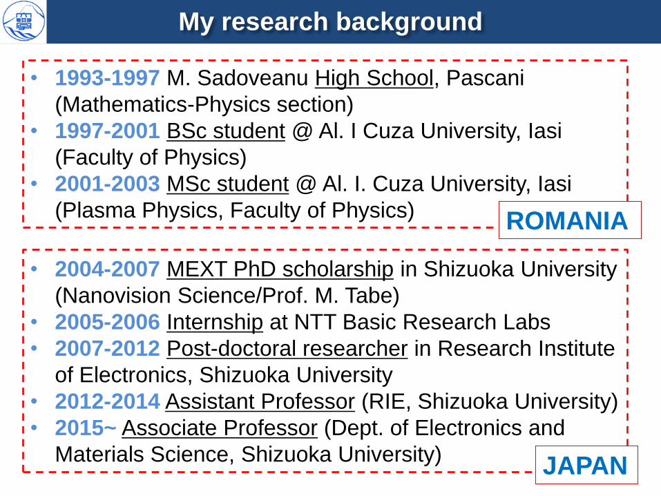
• 1993-1997 M. Sadoveanu High School, Pascani
(Mathematics-Physics section)
• 1997-2001 BSc student @ Al. I Cuza University, Iasi
(Faculty of Physics)
• 2001-2003 MSc student @ Al. I. Cuza University, Iasi
(Plasma Physics, Faculty of Physics)
My research background
• 2004-2007 MEXT PhD scholarship in Shizuoka University
(Nanovision Science/Prof. M. Tabe)
• 2005-2006 Internship at NTT Basic Research Labs
• 2007-2012 Post-doctoral researcher in Research Institute
of Electronics, Shizuoka University
• 2012-2014 Assistant Professor (RIE, Shizuoka University)
• 2015~ Associate Professor (Dept. of Electronics and
Materials Science, Shizuoka University)
ROMANIA
JAPAN
• My research work
Atomic/molecular-level electronics
Observation of atoms in nanodevices
• My experience in Japan:
PhD and post-doctoral researcher
Research grants: my insights
• My relation with Europe:
Collaboration networks
Double-degree programs for PhD
• Conclusions
Outline
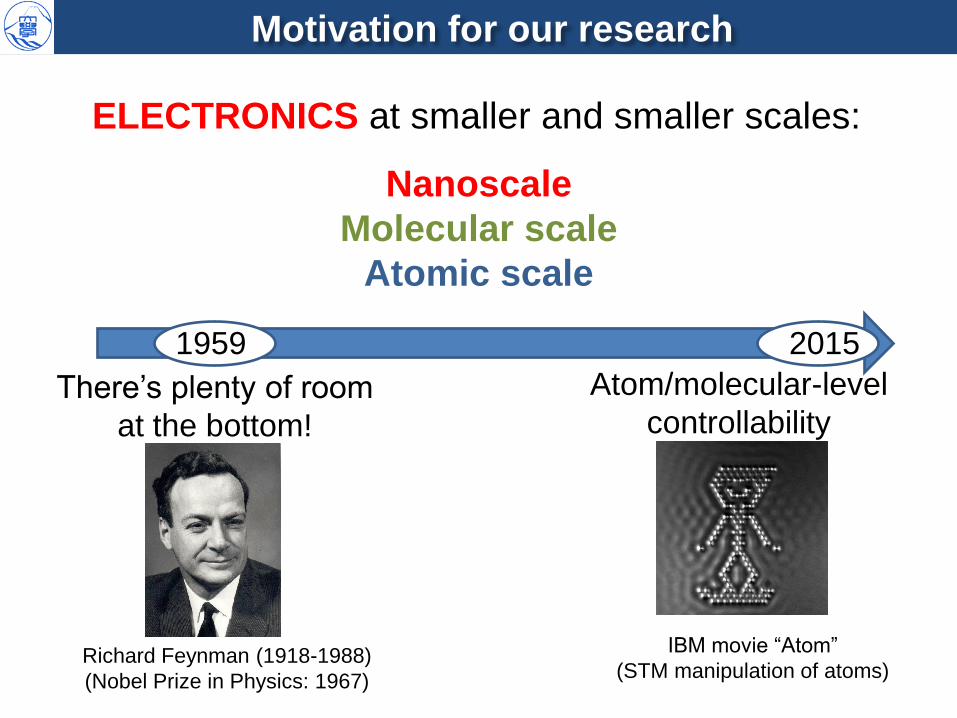
ELECTRONICS at smaller and smaller scales:
There’s plenty of room
at the bottom!
Richard Feynman (1918-1988)
(Nobel Prize in Physics: 1967)
IBM movie “Atom”
(STM manipulation of atoms)
Nanoscale
Molecular scale
Atomic scale
1959 2015
Atom/molecular-level
controllability
Motivation for our research
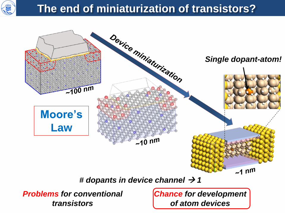
Moore’s
Law
# dopants in device channel 1
Problems for conventional
transistors
Chance for development
of atom devices
Single dopant-atom!
The end of miniaturization of transistors?

Gate voltage (V) D
rain
curr
ent
(A)
Individual Dopant Atom = Quantum Dot (QD)
Single-Dopant-Atom Transistor: concept
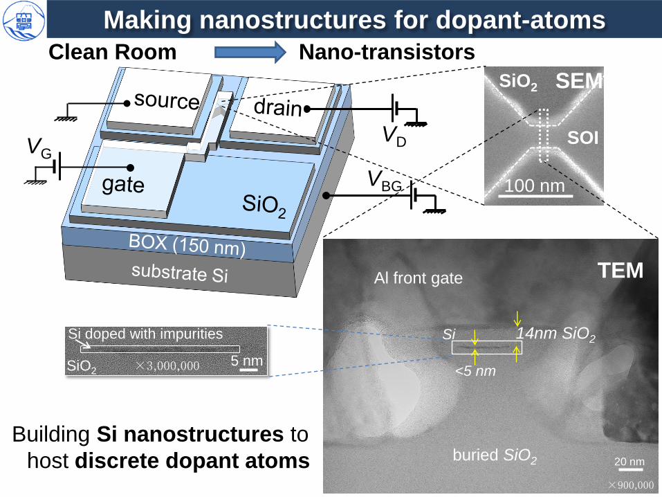
Making nanostructures for dopant-atoms
VD VG
VBG 100 nm
SOI
SiO2
SiO2
×900,000
20 nm
14nm SiO2
<5 nm
Si
×3,000,000 5 nm
Si doped with impurities
SiO2
Building Si nanostructures to
host discrete dopant atoms buried SiO2
Al front gate TEM
SEM
Clean Room Nano-transistors
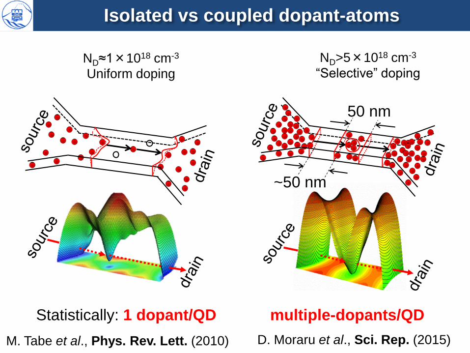
Isolated vs coupled dopant-atoms
50 nm
~50 nm
ND≈1×1018 cm-3
Uniform doping
ND>5×1018 cm-3
“Selective” doping
Statistically: 1 dopant/QD multiple-dopants/QD
M. Tabe et al., Phys. Rev. Lett. (2010) D. Moraru et al., Sci. Rep. (2015)

Measuring current through dopant-atoms
Single-electron tunneling
Variable-T I-V prober (T = 5~300 K)
Gate voltage (V)
Dra
in c
urr
ent
(A)
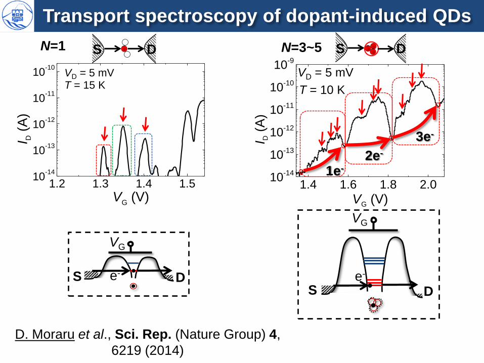
Transport spectroscopy of dopant-induced QDs
1.2 1.3 1.4 1.510
-14
10-13
10-12
10-11
10-10
I D (
A)
VG (V)
VD = 5 mV T = 15 K
N=1 S D
e- S D
VG
D. Moraru et al., Sci. Rep. (Nature Group) 4,
6219 (2014)
S D N=3~5
1.4 1.6 1.8 2.010
-14
10-13
10-12
10-11
10-10
10-9
I D (
A)
VG (V)
1e- 2e-
3e-
VD = 5 mV
T = 10 K
e- S D
VG
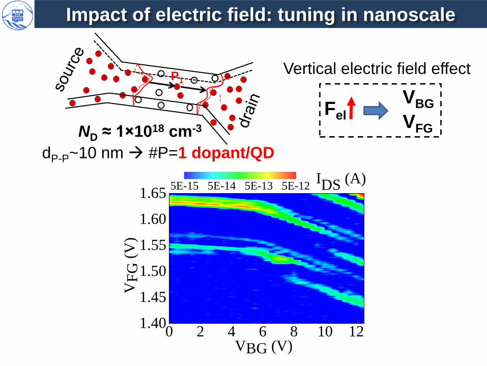
Impact of electric field: tuning in nanoscale
P1
dP-P~10 nm #P=1 dopant/QD
ND ≈ 1×1018 cm-3
Fel VBG
VFG
0 2 4 6 8 10 121.40
1.45
1.50
1.55
1.60
1.65IDS (A)
VBG (V)
VF
G (
V)
5E-15 5E-14 5E-13 5E-12
Vertical electric field effect
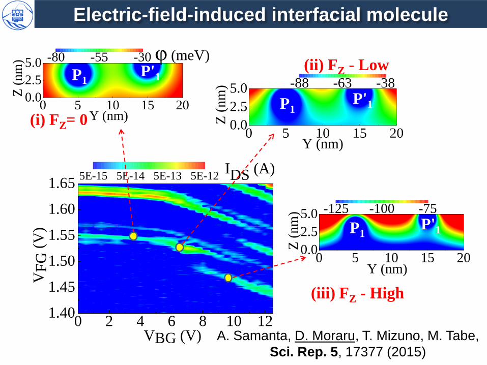
Electric-field-induced interfacial molecule
0 2 4 6 8 10 121.40
1.45
1.50
1.55
1.60
1.65IDS (A)
VBG (V)
VF
G (
V)
5E-15 5E-14 5E-13 5E-12
0 5 10 15 200.0
2.5
5.0 -80 -55 -30
Z (
nm
)
Y (nm)
P1 P'1
(i) FZ= 0
φ (meV)
0 5 10 15 200.0
2.5
5.0 -88 -63 -38
Z (
nm
)
Y (nm)
(ii) FZ - Low
P1 P'1
0 5 10 15 200.0
2.5
5.0 -125 -100 -75
Z (
nm
)
Y (nm)
(iii) FZ - High
P1 P'1
A. Samanta, D. Moraru, T. Mizuno, M. Tabe,
Sci. Rep. 5, 17377 (2015)
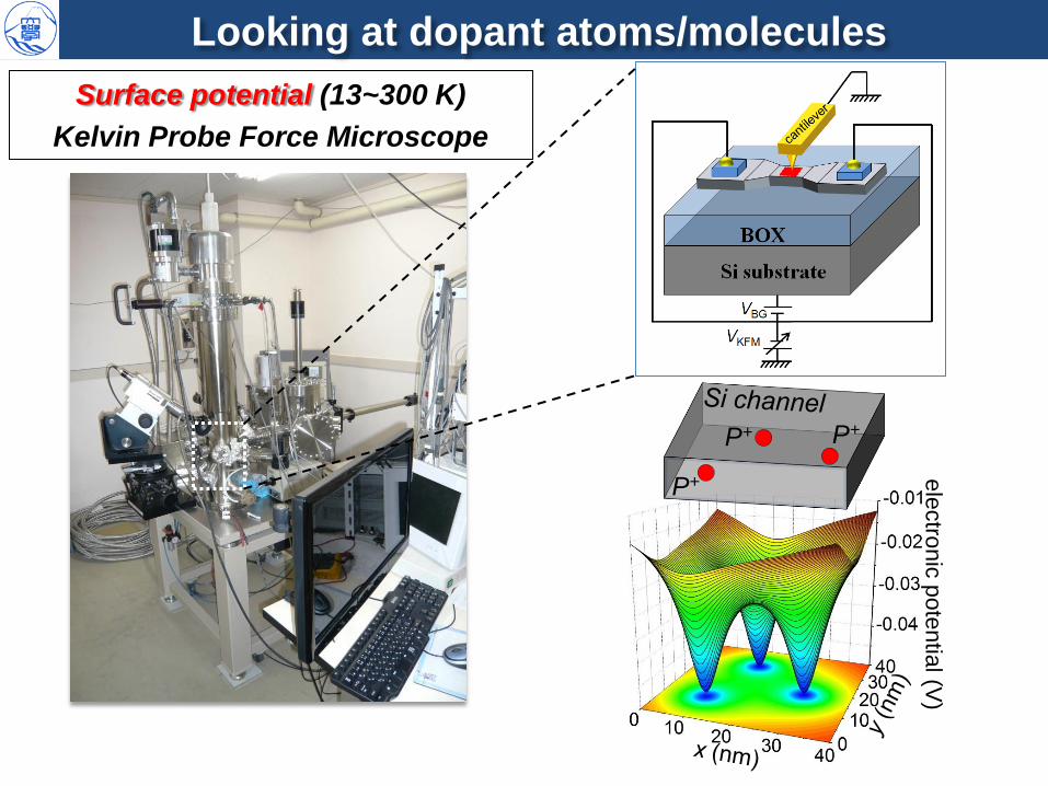
Looking at dopant atoms/molecules
Surface potential (13~300 K)
Kelvin Probe Force Microscope ele
ctro
nic
pote
ntia
l (V)
P+
P+ P+

VBG = 0 V
ele
ctr
on
ic p
ote
ntia
l (V
)
B
A
C
VBG = -1 V
ele
ctr
on
ic p
ote
ntia
l (V
)
B
A
C
VBG = -2 V
ele
ctr
on
ic p
ote
ntia
l (V
)
B
A
C
VBG = -3 V
ele
ctr
on
ic p
ote
ntia
l (V
)
Observation of e- injection in single dopants
A B C
-3V -2V
-1V 0V
3rd
2nd
B
A
C
1st
Localized electron injection in
individual P dopant-atoms
Low temperature: T = 13 K
M. Anwar, D. Moraru et al., Appl. Phys. Lett. 99, 213101 (2011)
K. Tyszka, D. Moraru et al., J. Appl. Phys. (2015); Appl. Phys. Express (2015)
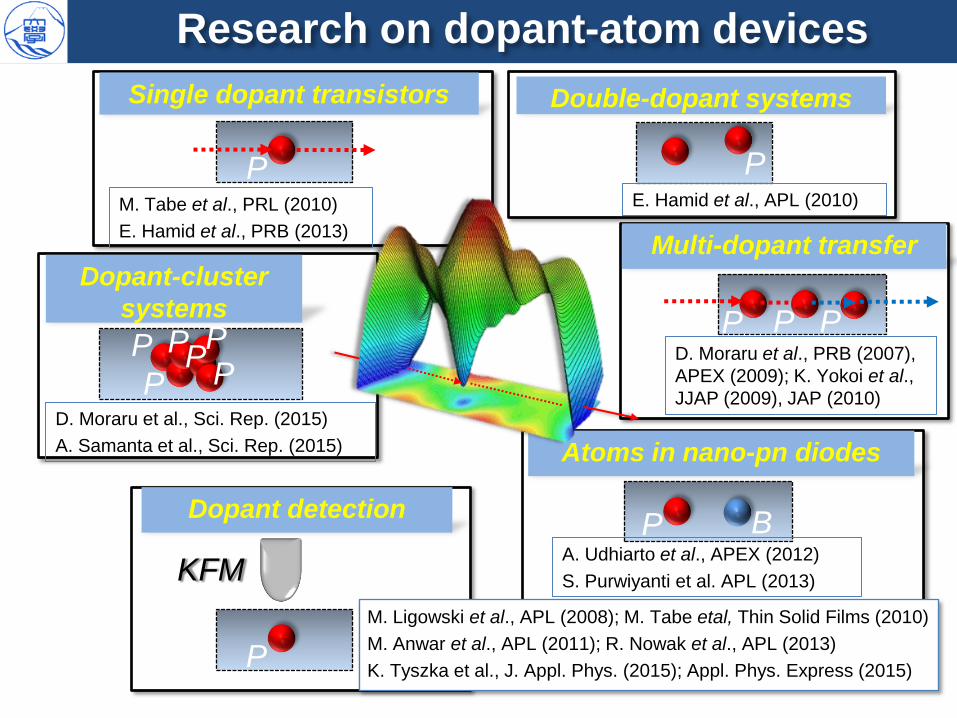
Single dopant transistors
P
Multi-dopant transfer
Dopant-cluster
systems
P
Dopant detection
P
Double-dopant systems
P
Research on dopant-atom devices
Atoms in nano-pn diodes
P P P
P B
M. Tabe et al., PRL (2010)
E. Hamid et al., PRB (2013)
D. Moraru et al., Sci. Rep. (2015)
A. Samanta et al., Sci. Rep. (2015)
E. Hamid et al., APL (2010)
D. Moraru et al., PRB (2007),
APEX (2009); K. Yokoi et al.,
JJAP (2009), JAP (2010)
A. Udhiarto et al., APEX (2012)
S. Purwiyanti et al. APL (2013)
M. Ligowski et al., APL (2008); M. Tabe etal, Thin Solid Films (2010)
M. Anwar et al., APL (2011); R. Nowak et al., APL (2013)
K. Tyszka et al., J. Appl. Phys. (2015); Appl. Phys. Express (2015)
KFM
P P P P
P
• My research work
Atomic/molecular-level electronics
Observation of atoms in nanodevices
• My experience in Japan:
PhD and post-doctoral researcher
Research grants: my insights
• My relation with Europe:
Collaboration networks
Double-degree programs for PhD
• Conclusions
Outline
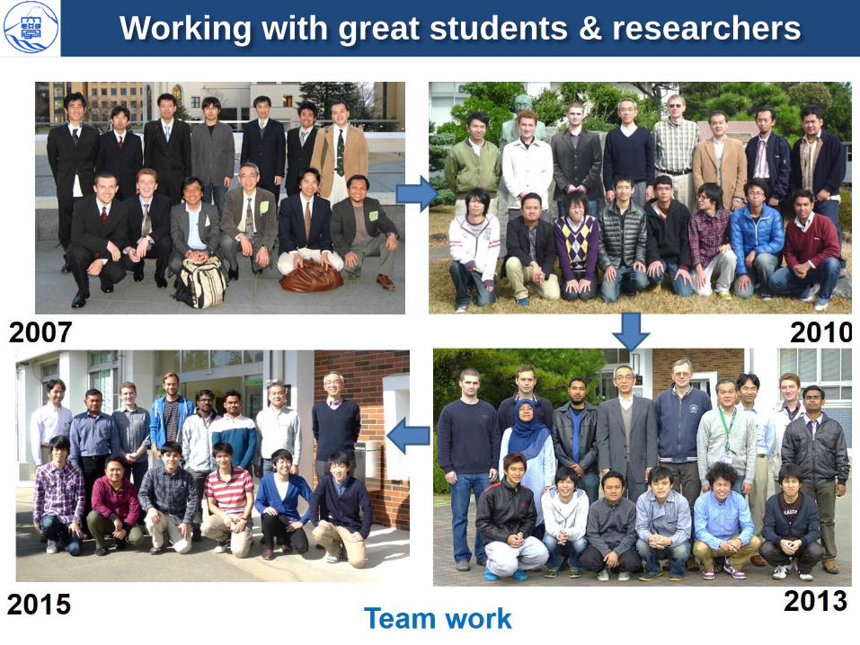
Working with great students & researchers
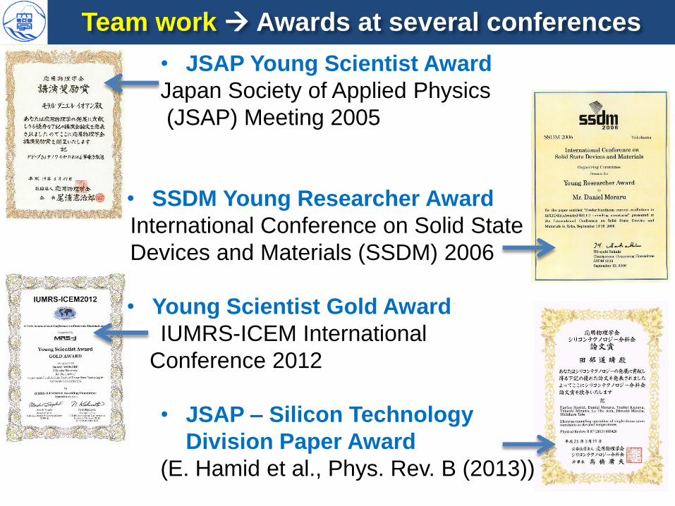
• JSAP Young Scientist Award
Japan Society of Applied Physics
(JSAP) Meeting 2005
• SSDM Young Researcher Award
International Conference on Solid State
Devices and Materials (SSDM) 2006
• Young Scientist Gold Award:
IUMRS-ICEM International
Conference 2012
• JSAP – Silicon Technology
Division Paper Award
(E. Hamid et al., Phys. Rev. B (2013))
Team work Awards at several conferences
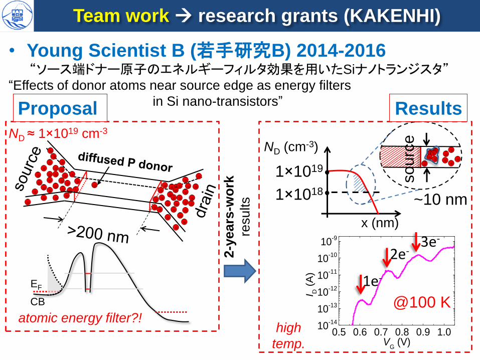
• Young Scientist B (若手研究B) 2014-2016 “ソース端ドナー原子のエネルギーフィルタ効果を用いたSiナノトランジスタ”
“Effects of donor atoms near source edge as energy filters
in Si nano-transistors”
Team work research grants (KAKENHI)
CB
EF
ND ≈ 1×1019 cm-3
2-y
ea
rs-w
ork
resu
lts
Proposal
atomic energy filter?! 0.5 0.6 0.7 0.8 0.9 1.0
10-14
10-13
10-12
10-11
10-10
10-9
I D (
A)
VG (V)
1e-
2e- 3e-
@100 K
1×10¹⁹
ND (cm-3)
1×10¹⁸
x (nm)
~10 nm
sourc
e
Results
high
temp.
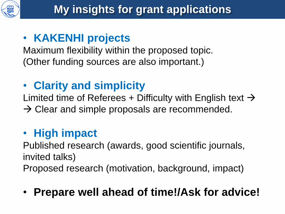
• KAKENHI projects Maximum flexibility within the proposed topic.
(Other funding sources are also important.)
• Clarity and simplicity Limited time of Referees + Difficulty with English text
Clear and simple proposals are recommended.
• High impact Published research (awards, good scientific journals,
invited talks)
Proposed research (motivation, background, impact)
• Prepare well ahead of time!/Ask for advice!
My insights for grant applications
• My research work
Atomic/molecular-level electronics
Observation of atoms in nanodevices
• My experience in Japan:
PhD and post-doctoral researcher
Research grants: my insights
• My relation with Europe:
Collaboration networks
Double-degree programs for PhD
• Conclusions
Outline
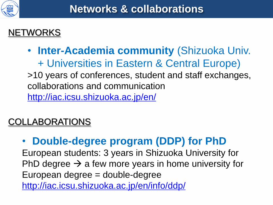
• Inter-Academia community (Shizuoka Univ.
+ Universities in Eastern & Central Europe) >10 years of conferences, student and staff exchanges,
collaborations and communication
http://iac.icsu.shizuoka.ac.jp/en/
Networks & collaborations
• Double-degree program (DDP) for PhD European students: 3 years in Shizuoka University for
PhD degree a few more years in home university for
European degree = double-degree
http://iac.icsu.shizuoka.ac.jp/en/info/ddp/
NETWORKS
COLLABORATIONS
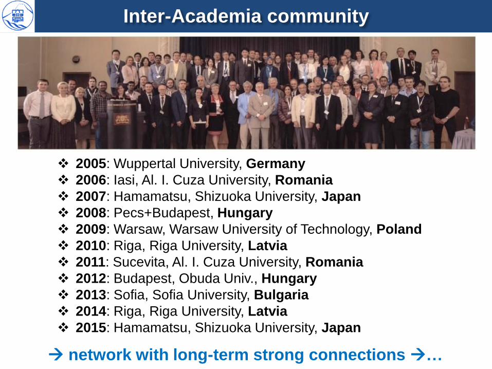
2005: Wuppertal University, Germany
2006: Iasi, Al. I. Cuza University, Romania
2007: Hamamatsu, Shizuoka University, Japan
2008: Pecs+Budapest, Hungary
2009: Warsaw, Warsaw University of Technology, Poland
2010: Riga, Riga University, Latvia
2011: Sucevita, Al. I. Cuza University, Romania
2012: Budapest, Obuda Univ., Hungary
2013: Sofia, Sofia University, Bulgaria
2014: Riga, Riga University, Latvia
2015: Hamamatsu, Shizuoka University, Japan
Inter-Academia community
network with long-term strong connections …
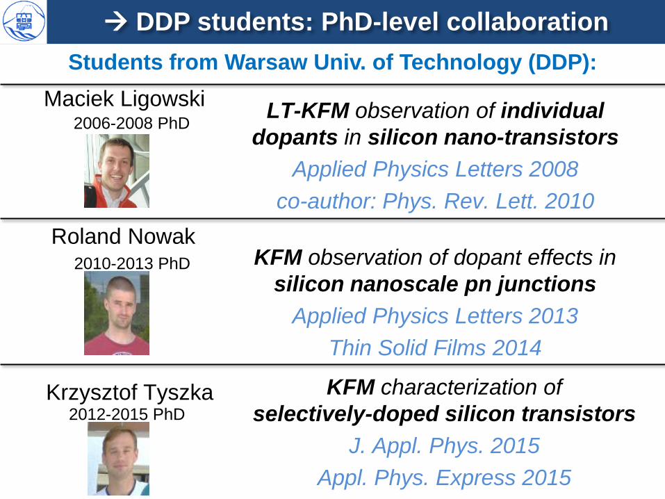
DDP students: PhD-level collaboration
Maciek Ligowski LT-KFM observation of individual
dopants in silicon nano-transistors
Applied Physics Letters 2008
co-author: Phys. Rev. Lett. 2010
KFM observation of dopant effects in
silicon nanoscale pn junctions
Applied Physics Letters 2013
Thin Solid Films 2014
Roland Nowak
Krzysztof Tyszka KFM characterization of
selectively-doped silicon transistors
J. Appl. Phys. 2015
Appl. Phys. Express 2015
2006-2008 PhD
2010-2013 PhD
2012-2015 PhD
Students from Warsaw Univ. of Technology (DDP):
• My research work
Atomic/molecular-level electronics
Observation of atoms in nanodevices
• My experience in Japan:
PhD and post-doctoral researcher
Research grants: my insights
• My relation with Europe:
Collaboration networks
Double-degree programs for PhD
• Conclusions
Outline

• Research work
Choose research directions of high impact
Clearly define your original approach
• Experience in Japan:
Team work within international groups
Research grants: high impact + timely preparation
• Relation with Europe:
Build and sustain long-term networks
Focus on PhD-level collaborations
Conclusions
Thank you for your attention!