data sheet - arm information centerinfocenter.arm.com/help/topic/com.arm.doc.ddi0027d/ddi...preface...
TRANSCRIPT

Advanced RISC Machines
ARM
Document Number: ARM DDI 0027D
Issued: Dec 1994
Copyright Advanced RISC Machines Ltd (ARM) 1994
All rights reserved
ARM7DIData Sheet
Proprietary NoticeARM, the ARM Powered logo, BlackICE and ICEbreaker are trademarks of Advanced RISCMachines Ltd.
Neither the whole nor any part of the information contained in, or the product described in, thisdatasheet may be adapted or reproduced in any material form except with the prior writtenpermission of the copyright holder.
The product described in this datasheet is subject to continuous developments andimprovements. All particulars of the product and its use contained in this datasheet are given byARM in good faith. However, all warranties implied or expressed, including but not limited toimplied warranties or merchantability, or fitness for purpose, are excluded.
This datasheet is intended only to assist the reader in the use of the product. ARM Ltd shall notbe liable for any loss or damage arising from the use of any information in this datasheet, or anyerror or omission in such information, or any incorrect use of the product.
Change LogIssue Date By Change
A July 1994 EH Created.B Aug 94 BJH Updated Instruction Cycle OperationsC Oct 94 EH Sources repaired: no material changes to textD Dec 94 PB Edited.

Preface
iv ARM7DI Data Sheet
The ARM7DI is a low-power, general purpose 32-bit RISC microprocessor with integrated debug support.It comprises the ARM7D CPU core, and ICEbreaker module and a TAP controller. Its simple, elegant andfully static design is particularly suitable for cost and power sensitive applications.
EnhancementsThe ARM7DI is similar to the ARM6 but with the following enhancements:
■ advanced debug (integrated ICE) support for faster time to market■ fabrication on a sub-micron process for increased speed and reduced power consumption■ 3V operation, for very low power consumption, as well as 5V operation for system compatibility■ higher clock speedfor faster program execution.
ApplicationsThe ARM7DI is ideally suited to those applications requiring RISC performance from a compact,power-efficient processor. These include:
Telecomms GSM terminal controller
Datacomms Protocol conversion
Portable Computing Palmtop computer
Portable InstrumentS Handheld data acquisition unit
Automotive Engine management unit
Information Systems Smart cards
Imaging JPEG controller
Feature Summary■ 32-bit RISC processor (32-bit data & address bus)■ Advanced debug
fully integrated ICE
■ Big and Little Endian operating modes■ High performance RISC■ Low power consumption■ Fully static operation
ideal for power-sensitive applications
■ Fast interrupt responsefor real-time applications
■ Virtual Memory System Support■ Excellent high-level language support■ Simple but powerful instruction set
InstructionDecoder
&Logic
Control
Address Register
AddressIncrementer
Register Bank
BarrelShifter
32 bit ALU
Write Data Register
InstructionPipeline &Read DataRegister
Booth’sMultiplierD
ebug
ICEbreaker TAP controller

i
Table of Contents
1.0 Introduction 51.1 ARM7DI Block Diagram 61.2 ARM7D Core Diagram 71.3 ARM7DI Functional Diagram 8
2.0 Signal Description 9
3.0 Programmer's Model 153.1 Hardware Configuration Signals 153.2 Operating Mode Selection 163.3 Registers 173.4 Exceptions 203.5 Reset 24
4.0 Instruction Set 254.1 Instruction Set Summary 254.2 The Condition Field 264.3 Branch and Branch with link (B, BL) 274.4 Data processing 294.5 PSR Transfer (MRS, MSR) 364.6 Multiply and Multiply-Accumulate (MUL, MLA) 404.7 Single data transfer (LDR, STR) 424.8 Block Data Transfer (LDM, STM) 484.9 Single data swap (SWP) 554.10 Software interrupt (SWI) 574.11 Coprocessor data operations (CDP) 594.12 Coprocessor data transfers (LDC, STC) 614.13 Coprocessor register transfers (MRC, MCR) 644.14 Undefined instruction 664.15 Instruction Set Examples 67
5.0 Memory Interface 715.1 Cycle types 715.2 Byte addressing 725.3 Address timing 745.4 Memory management 745.5 Locked operations 755.6 Stretching access times 755.7 The External Data Bus 76
6.0 Coprocessor Interface 816.1 Interface signals 816.2 Data transfer cycles 826.3 Register transfer cycle 826.4 Privileged instructions 826.5 Idempotency 836.6 Undefined instructions 83
7.0 Debug Interface 857.1 Overview 857.2 Debug Systems 857.3 Debug Interface Signals 86

ARM7DI Data Sheet
ii
7.4 Scan Chains and JTAG Interface 897.5 Reset 917.6 Pullup Resistors 917.7 Instruction Register 927.8 Public Instructions 927.9 Test Data Registers 947.10 ARM7DI Core Clocks 997.11 Determining the Core and System State 1007.12 The PC's Behaviour During Debug 1037.13 Priorities / Exceptions 1057.14 Scan Interface Signals 106
8.0 The ARM7DI ICEBreaker Module 1098.1 The Watchpoint Registers 1108.2 The Debug Control Register 1158.3 Debug Status Register 1168.4 Coupling Breakpoints and Watchpoints 1198.5 Disabling ICEbreaker 1208.6 ICEbreaker Timing 1208.7 ICEBreaker Programming Restriction 120
9.0 Instruction Cycle Operations 1219.1 Branch and branch with link 1219.2 Data Operations 1219.3 Multiply and multiply accumulate 1239.4 Load register 1239.5 Store register 1249.6 Load multiple registers 1259.7 Store multiple registers 1279.8 Data swap 1279.9 Software interrupt and exception entry 1289.10 Coprocessor data operation 1299.11 Coprocessor data transfer (from memory to coprocessor) 1299.12 Coprocessor data transfer (from coprocessor to memory) 1319.13 Coprocessor register transfer (Load from coprocessor) 1329.14 Coprocessor register transfer (Store to coprocessor) 1329.15 Undefined instructions and coprocessor absent 1339.16 Unexecuted instructions 1349.17 Instruction Speed Summary 134
10.0 DC Parameters 13710.1 Absolute Maximum Ratings 13710.2 DC Operating Conditions: 137
11.0 AC Parameters 139
12.0 Appendix - Backward Compatibility 149
Introduction
5
1.0 Introduction
The ARM7DI is part of the Advanced RISC Machines (ARM) family of general purpose 32-bitmicroprocessors, which offer very low power consumption and price for high performance devices. Thearchitecture is based on Reduced Instruction Set Computer (RISC) principles, and the instruction set andrelated decode mechanism are much simpler in comparison with microprogrammed Complex InstructionSet Computers. This results in a high instruction throughput and impressive real-time interrupt responsefrom a small and cost-effective chip.
The instruction set comprises eleven basic instruction types:
• Two of these make use of the on-chip arithmetic logic unit, barrel shifter and multiplier to performhigh-speed operations on the data in a bank of 31 registers, each 32 bits wide;
• Three classes of instruction control data transfer between memory and the registers, one optimisedfor flexibility of addressing, another for rapid context switching and the third for swapping data;
• Three instructions control the flow and privilege level of execution; and
• Three types are dedicated to the control of external coprocessors which allow the functionality ofthe instruction set to be extended off-chip in an open and uniform way.
The ARM instruction set is a good target for compilers of many different high-level languages. Whererequired for critical code segments, assembly code programming is also straightforward, unlike some RISCprocessors which depend on sophisticated compiler technology to manage complicated instructioninterdependencies.
Pipelining is employed so that all parts of the processing and memory systems can operate continuously.Typically, while one instruction is being executed, its successor is being decoded, and a third instruction isbeing fetched from memory.
The memory interface has been designed to allow the performance potential to be realised withoutincurring high costs in the memory system. Speed critical control signals are pipelined to allow systemcontrol functions to be implemented in standard low-power logic, and these control signals facilitate theexploitation of the fast local access modes offered by industry standard dynamic RAMs.
ARM7DI has a 32 bit address bus. All ARM processors share the same instruction set, and ARM7DI can beconfigured to use a 26 bit address bus for backwards compatibility with earlier processors.
ARM7DI is a fully static CMOS implementation of the ARM which allows the clock to be stopped in anypart of the cycle with extremely low residual power consumption and no loss of state.
Notation:
0x - marks a Hexadecimal quantityBOLD - external signals are shown in bold capital lettersbinary - where it is not clear that a quantity is binary it is followed by the word binary

ARM7DI Data Sheet
6
1.1 ARM7DI Block Diagram
Figure 1: ARM7DI Block Diagram
ARM7DIICEbreaker
ARM7DITAP Controller
•
•
Scan Chain 0Scan Chain 2
A[31:0]
ARM7DCore
Scan Chain 1D[31:0]
nOPCnRWnBW
AllOther
Signals
TCK TMS TDInTRST TDO
EXTERN1
EXTERN0
nTRANSnMREQ

Introduction
7
1.2 ARM7D Core Diagram
Figure 2: ARM7D Core Diagram
LATEABTA
nRESET
nMREQ
SEQ
ABORT
nIRQ
nFIQ
nRW
nBW
LOCKnCPI
CPA
CPB
nWAIT
MCLK
nOPC
nTRANS
DATA32
BIGEND
PROG32
InstructionDecoder
&ControlLogic
Instruction Pipeline& Read Data Register
DBE
D[31:0]
32 bit ALU
BarrelShifter
A
AddressIncrementer
Address Register
Register Bank(31 x 32bit registers)(6 status registers)
A[31:0]
ALE
Incrementer
Bus
PC
Bus
LU
Bus
bus
B
bus
Multiplier
ABE
Write Data Register
nM[4:0]
Booth’s
nENOUT nENIN
TBE
ScanControl
DBGRQ int
BREAKPT int
nEXEC
DBGACK int
ISYNC
ECLK

ARM7DI Data Sheet
8
1.3 ARM7DI Functional Diagram
Figure 3: ARM7DI Functional Diagram
nRW
nBW
LOCK
A[31:0]
nMREQ
SEQ
ABORT
MemoryManagement
nOPC
nCPI
CPA
CPB
CoprocessorInterface
nTRANS
MemoryInterface
Interface
D[31:0]
TCK
TMS
TDI
nTRST
BoundaryScan
TDO
ARM7DI
nM[4:0]ProcessorMode
ALE
nIRQ
nFIQ
Bus
InterruptsISYNC
nRESET
MCLKnWAITClocks
VDD
VSSPower
DBGRQ
BREAKPT
DBGACKnEXEC
Debug
Controls
PROG32
DATA32
BIGEND
Configuration
ABE
EXTERN 1
DBE
TBE
EXTERN 0
nENOUT
nENIN
ECLK
DBGEN

Signal Description
9
2.0 Signal Description
Name Type Description
A[31:0] O8 Addresses. This is the processor address bus. If ALE (address latch enable) isHIGH, the addresses become valid during phase 2 of the cycle before the one towhich they refer and remain so during phase 1 of the referenced cycle. Theirstable period may be controlled by ALE as described below.
ABE IC Address bus enable. This is an input signal which, when LOW, puts the addressbus drivers into a high impedance state. This signal has a similar effect on thefollowing control signals: nBW, nRW, LOCK, nOPC and nTRANS. ABE mustbe tied HIGH when there is no system requirement to turn off the addressdrivers.
ABORT IC Memory Abort. This is an input which allows the memory system to tell theprocessor that a requested access is not allowed.
ALE IC Address latch enable. This input is used to control transparent latches on theaddress outputs. Normally the addresses change during phase 2 to the valuerequired during the next cycle, but for direct interfacing to ROMs they arerequired to be stable to the end of phase 2. Taking ALE LOW until the end ofphase 2 will ensure that this happens. This signal has a similar effect on thefollowing control signals: nBW, nRW, LOCK, nOPC and nTRANS. If thesystem does not require address lines to be held in this way, ALE must be tiedHIGH. The address latch is static, so ALE may be held LOW for long periods tofreeze addresses.
BIGEND IC Big Endian configuration. When this signal is HIGH the processor treats bytesin memory as being in Big Endian format. When it is LOW memory is treatedas Little Endian. ARM processors which do not have selectable Endianism(ARM2, ARM2aS, ARM3, ARM61) are Little Endian.
BREAKPT IC Breakpoint. This signal allows external hardware to halt the execution of theprocessor for debug purposes. When HIGH causes the current memory accessto be breakpointed. If the memory access is an instruction fetch, ARM7DI willenter debug state if the instruction reaches the execute stage of the ARM7DIpipeline. If the memory access is for data, ARM7DI will enter debug state afterthe current instruction completes execution.This allows extension of theinternal breakpoints provided by the ICEBreaker module. See Chapter 8.0 TheARM7DI ICEBreaker Module.
CPA IC Coprocessor absent. A coprocessor which is capable of performing theoperation that ARM7DI is requesting (by asserting nCPI) should take CPALOW immediately. If CPA is HIGH at the end of phase 1 of the cycle in whichnCPI went LOW, ARM7DI will abort the coprocessor handshake and take theundefined instruction trap. If CPA is LOW and remains LOW, ARM7DI willbusy-wait until CPB is LOW and then complete the coprocessor instruction.
Table 1: Signal Description

ARM7DI Data Sheet
10
CPB IC Coprocessor busy. A coprocessor which is capable of performing the operationwhich ARM7DI is requesting (by asserting nCPI), but cannot commit to startingit immediately, should indicate this by driving CPB HIGH. When thecoprocessor is ready to start it should take CPB LOW. ARM7DI samples CPBat the end of phase 1 of each cycle in which nCPI is LOW.
D[31:0] IC/O8 Data Bus. These are bidirectional signal paths which are used for data transfersbetween the processor and external memory. During read cycles (when nRW isLOW), the input data must be valid before the end of phase 2 of the transfercycle. During write cycles (when nRW is HIGH), the output data will becomevalid during phase 1 and remain valid throughout phase 2 of the transfer cycle.
DATA32 IC 32 bit Data configuration. When this signal is HIGH the processor can accessdata in a 32 bit address space using address lines A[31:0]. When it is LOW theprocessor can access data from a 26 bit address space using A[25:0]. In this latterconfiguration the address lines A[31:26] are not used. Before changingDATA32, ensure that the processor is not about to access an address greater that0x3FFFFFF in the next cycle.
DBE IC Internal Data Bus Enable. This is an input signal which, when driven LOW,puts the internal data bus (the bus between the core logic and the pads) into thehigh impedance state. This is included for test purposes, and should be tiedHIGH at all times.
DBGACK O4 Debug acknowledge. When HIGH indicates ARM is in debug state.
DBGEN IC Debug Enable. This input signal allows the debug features of ARM7DI to bedisabled. This signal should be driven LOW when debugging is not required.
DBGRQ IC Debug request. This is a level-sensitive input, which when HIGH causesARM7DI to enter debug state after executing the current instruction. Thisallows external hardware to force ARM7DI into the debug state, in addition tothe debugging features provided by the ICEBreaker block. See Chapter 8.0 TheARM7DI ICEBreaker Module for details.
ECLK O4 External clock output. In normal operation, this is simply MCLK (optionallystretched with nWAIT) exported from the core. When the core is being de-bugged, this is DCLK. This allows external hardware to track when theARM7DI core is clocked.
EXTERN1 IC External input 1. This is an input to the ICEBreaker logic in the ARM7DI whichallows breakpoints and/or watchpoints to be dependent on an external condi-tion.
EXTERN0 IC External input 0. This is an input to the ICEBreaker logic in the ARM7DI whichallows breakpoints and/or watchpoints to be dependent on an external condi-tion.
HIGHZ O4 This signal denotes that the HIGHZ instruction has been loaded into the TAPcontroller. See Chapter 7.0 Debug Interface for details.
Name Type Description
Table 1: Signal Description (Continued)

Signal Description
11
ISYNC IC Synchronous interrupts. When LOW indicates that the nIRQ and nFIQ inputsare to be synchronised by the ARM core. When HIGH disables thissynchronisation for inputs that are already synchronous.
LOCK O8 Locked operation. When LOCK is HIGH, the processor is performing a“locked” memory access, and the memory controller must wait until LOCKgoes LOW before allowing another device to access the memory. LOCKchanges while MCLK is HIGH, and remains HIGH for the duration of thelocked memory accesses. It is active only during the data swap (SWP)instruction. The timing of this signal may be modified by the use of ALE in asimilar way to the address, please refer to the ALE description. This signal mayalso be driven to a high impedance state by driving ABE LOW.
MCLK IC Memory clock input. This clock times all ARM7DI memory accesses and inter-nal operations. The clock has two distinct phases - phase 1 in which MCLK isLOW and phase 2 in which MCLK (and nWAIT) is HIGH. The clock may bestretched indefinitely in either phase to allow access to slow peripherals ormemory. Alternatively, the nWAIT input may be used with a free runningMCLK to achieve the same effect.
nBW O8 Not byte/word. This is an output signal used by the processor to indicate tothe external memory system when a data transfer of a byte length is required.The signal is HIGH for word transfers and LOW for byte transfers and is validfor both read and write cycles. The signal will become valid during phase 2 ofthe cycle before the one in which the transfer will take place. It will remain sta-ble throughout phase 1 of the transfer cycle. The timing of this signal may bemodified by the use of ALE in a similar way to the address, please refer to theALE description. This signal may also be driven to a high impedance state bydriving ABE LOW.
nCPI O4 Not Coprocessor instruction. When ARM7DI executes a coprocessorinstruction, it will take this output LOW and wait for a response from thecoprocessor. The action taken will depend on this response, which thecoprocessor signals on the CPA and CPB inputs.
nENIN IC NOT enable input. This signal may be used in conjunction with nENOUT tocontrol the data bus during write cycles. See Chapter 5.0 Memory Interface.
nENOUT O4 Not enable output. During a data write cycle, this signal is driven low duringphase 1, and remains low for the entire cycle. This may be used to aidarbitration in shared bus applications. See Chapter 5.0 Memory Interface.
nEXEC O4 Not executed. When HIGH indicates that the instruction in the execution unitis not being executed, because for example it has failed its condition code check.
nFIQ IC Not fast interrupt request. This is an interrupt request to the processor whichcauses it to be interrupted if taken LOW when the appropriate enable in theprocessor is active. The signal is level-sensitive and must be held LOW until asuitable response is received from the processor. nFIQ may be synchronous orasynchronous, depending on the state of ISYNC.
Name Type Description
Table 1: Signal Description (Continued)

ARM7DI Data Sheet
12
nIRQ IC Not interrupt request. As nFIQ, but with lower priority. May be taken LOW tointerrupt the processor when the appropriate enable is active. nIRQ may besynchronous or asynchronous, depending on the state of ISYNC.
nM[4:0] O4 Not processor mode. These are output signals which are the inverses of theinternal status bits indicating the processor operation mode.
nMREQ O4 Not memory request. This signal, when LOW, indicates that the processorrequires memory access during the following cycle. The signal becomes validduring phase 1, remaining valid through phase 2 of the cycle preceding that towhich it refers.
nOPC O8 Not op-code fetch. When LOW this signal indicates that the processor isfetching an instruction from memory; when HIGH, data (if present) is beingtransferred. The signal becomes valid during phase 2 of the previous cycle,remaining valid through phase 1 of the referenced cycle. The timing of thissignal may be modified by the use of ALE in a similar way to the address, pleaserefer to the ALE description. This signal may also be driven to a highimpedance state by driving ABE LOW.
nRESET IC Not reset. This is a level sensitive input signal which is used to start theprocessor from a known address. A LOW level will cause the instruction beingexecuted to terminate abnormally. When nRESET becomes HIGH for at leastone clock cycle, the processor will re-start from address 0. nRESET mustremain LOW (and nWAIT must remain HIGH) for at least two clock cycles.During the LOW period the processor will perform dummy instruction fetcheswith the address incrementing from the point where reset was activated. Theaddress will overflow to zero if nRESET is held beyond the maximum addresslimit.
nRW O8 Not read/write. When HIGH this signal indicates a processor write cycle; whenLOW, a read cycle. It becomes valid during phase 2 of the cycle before that towhich it refers, and remains valid to the end of phase 1 of the referenced cycle.The timing of this signal may be modified by the use of ALE in a similar way tothe address, please refer to the ALE description. This signal may also be drivento a high impedance state by driving ABE LOW.
nTDOEN O4 Not TDO Enable. When LOW, this signal denotes that serial data is beingdriven out on the TDO output. nTDOEN would normally be used as an outputenable for a TDO pin in a packaged part.
nTRANS O8 Not memory translate. When this signal is LOW it indicates that the processoris in user mode. It may be used to tell memory management hardware whentranslation of the addresses should be turned on, or as an indicator of non-usermode activity. The timing of this signal may be modified by the use of ALE ina similar way to the address, please refer to the ALE description. This signalmay also be driven to a high impedance state by driving ABE LOW.
Name Type Description
Table 1: Signal Description (Continued)

Signal Description
13
Key to Signal Types:
IC - Input CMOS thresholds P - PowerO4 - Output with INV4 driver O8 - Output with INV8 driver
nTRST I NOT Test Reset. Active-low reset signal for the boundary scan logic. This pinmust be pulsed or driven low to achieve normal device operation, in additionto the normal device reset (nRESET). The action of this and the other fourboundary scan signals are described in more detail later in this document.
nWAIT I Not wait. When accessing slow peripherals, ARM7DI can be made to wait foran integer number of MCLK cycles by driving nWAIT LOW. Internally,nWAIT is ANDed with MCLK and must only change when MCLK is LOW. IfnWAIT is not used it must be tied HIGH.
PROG32 I 32 bit Program configuration. When this signal is HIGH the processor can fetchinstructions from a 32 bit address space using address lines A[31:0]. When it isLOW the processor fetches instructions from a 26 bit address space usingA[25:0]. In this latter configuration the address lines A[31:26] are not used forinstruction fetches. Before changing PROG32, ensure that the processor is in a26 bit mode, and is not about to write to an address in the range 0 to 0x1F(inclusive) in the next cycle.
SEQ O4 Sequential address. This output signal will become HIGH when the address ofthe next memory cycle will be related to that of the last memory access. The newaddress will either be the same as or 4 greater than the old one.
The signal becomes valid during phase 1 and remains so through phase 2 of thecycle before the cycle whose address it anticipates. It may be used, incombination with the low-order address lines, to indicate that the next cycle canuse a fast memory mode (for example DRAM page mode) and/or to bypass theaddress translation system.
TBE IC Test Bus Enable. When driven LOW, TBE forces the data bus D[31:0], theAddress bus A[31:0], plus LOCK, nBW, nRW, nTRANS and nOPC to highimpedance. This is as if both ABE and DBE had both been driven LOW.However, TBE does not have an asssociated scan cell and so allows externalsignls to be driven high impedance during scan testing. Under normaloperating conditions, TBE should be held HIGH at all times.
TCK IC Test Clock.
TDI IC Test Data Input.
TDO O Test Data Output. Output from the boundary scan logic.
TMS IC Test Mode Select.
VDD P Power supply. These connections provide power to the device.
VSS P Ground. These connections are the ground reference for all signals.
Name Type Description
Table 1: Signal Description (Continued)

ARM7DI Data Sheet
14
Note:For a 0.8 µm ARM7DI:INV4 driver has transistor sizes of p = 29.76 µm/0.8 µm; N = 16.96 µm/0.8 µmINV8 driver has transistor sizes of p = 47.04 µm/0.8 µm; N = 33.6 µm/0.8 µm

Programmer's Model
15
3.0 Programmer's Model
ARM7DI supports a variety of operating configurations. Some are controlled by inputs and are known asthe hardware configurations. Others may be controlled by software and these are known as operating modes.
3.1 Hardware Configuration Signals
The ARM7DI processor provides 3 hardware configuration signals which may be changed while theprocessor is running and which are discussed below.
3.1.1 Big and Little Endian
The BIGEND input sets whether the ARM7DI treats words in memory as being stored in Big Endian orLittle Endian format. Memory is viewed as a linear collection of bytes numbered upwards from zero. Bytes0 to 3 hold the first stored word, bytes 4 to 7 the second and so on.
In the Little Endian scheme the lowest numbered byte in a word is considered to be the least significant byteof the word and the highest numbered byte is the most significant. Byte 0 of the memory system should beconnected to data lines 7 through 0 (D[7:0]) in this scheme.
In the Big Endian scheme the most significant byte of a word is stored at the lowest numbered byte and theleast significant byte is stored at the highest numbered byte. Byte 0 of the memory system should thereforebe connected to data lines 31 through 24 (D[31:24]). Load and store are the only instructions affected by theendian-ness: see Section 4.7: Single data transfer (LDR, STR) on page 42 for more details.
Little Endian
Higher Address 31 24 23 16 15 8 7 0 Word Address
11 10 9 8 8
7 6 5 4 4
3 2 1 0 0
Lower Address
• Least significant byte is at lowest address
• Word is addressed by byte address of least significant byte
Figure 4: Little Endian addresses of bytes within words

ARM7DI Data Sheet
16
3.1.2 Configuration Bits for Backward Compatibility
The other two inputs, PROG32 and DATA32 are used for backward compatibility with earlier ARMprocessors (see 12.0: Appendix - Backward Compatibility) but should normally be set to 1. This configurationextends the address space to 32 bits, introduces major changes in the programmer's model as describedbelow, and provides support for running existing 26 bit programs in the 32 bit environment. This mode isrecommended for compatibility with future ARM processors and all new code should be written to useonly the 32 bit operating modes.
Because the original ARM instruction set has been modified to accommodate 32 bit operation there arecertain additional restrictions which programmers must be aware of. These are indicated in the text by thewords shall and shall not. Reference should also be made to the ARM Application Notes “Rules for ARM CodeWriters” and “Notes for ARM Code Writers”, available from your supplier.
3.2 Operating Mode Selection
ARM7DI has a 32 bit data bus and a 32 bit address bus. The processor supports byte (8 bit) and word (32 bit)data types, where words must be aligned to four byte boundaries. Instructions are exactly one word long,and data operations (eg ADD) are only performed on word quantities. Load and store operations cantransfer either bytes or words.
Big Endian
Higher Address 31 24 23 16 15 8 7 0 Word Address
8 9 10 11 8
4 5 6 7 4
0 1 2 3 0
Lower Address
• Most significant byte is at lowest address
• Word is addressed by byte address of most significant byte
Figure 5: Big Endian addresses of bytes within words

Programmer's Model
17
ARM7DI supports six modes of operation:
(1) User mode (usr): the normal program execution state
(2) FIQ mode (fiq): designed to support a data transfer or channel process
(3) IRQ mode (irq): used for general purpose interrupt handling
(4) Supervisor mode (svc): a protected mode for the operating system
(5) Abort mode (abt): entered after a data or instruction prefetch abort
(6) Undefined mode (und): entered when an undefined instruction is executed
Mode changes may be made under software control or may be brought about by external interrupts orexception processing. Most application programs will execute in User mode. The other modes, known asprivileged modes, will be entered to service interrupts or exceptions or to access protected resources.
3.3 Registers
The processor has a total of 37 registers made up of 31 general 32 bit registers and 6 status registers. At anyone time 16 general registers (R0 to R15) and one or two status registers are visible to the programmer. Thevisible registers depend on the processor mode. The other registers, known as the banked registers, areswitched in to support IRQ, FIQ, Supervisor, Abort and Undefined mode processing. Figure 6: RegisterOrganisation shows how the registers are arranged, with the banked registers shaded.
In all modes 16 registers, R0 to R15, are directly accessible. All registers except R15 are general purpose andmay be used to hold data or address values. Register R15 holds the Program Counter (PC). When R15 isread, bits [1:0] are zero and bits [31:2] contain the PC. A seventeenth register (the CPSR - Current ProgramStatus Register) is also accessible. It contains condition code flags and the current mode bits and may bethought of as an extension to the PC.
R14 is used as the subroutine link register and receives a copy of R15 when a Branch and Link instructionis executed. It may be treated as a general purpose register at all other times. R14_svc, R14_irq, R14_fiq,R14_abt and R14_und are used similarly to hold the return values of R15 when interrupts and exceptionsarise, or when Branch and Link instructions are executed within interrupt or exception routines.

ARM7DI Data Sheet
18
Figure 6: Register Organisation
FIQ mode has seven banked registers mapped to R8-14 (R8_fiq-R14_fiq). Many FIQ programs will not needto save any registers. User mode, IRQ mode, Supervisor mode, Abort mode and Undefined mode each havetwo banked registers mapped to R13 and R14. The two banked registers allow these modes to each have aprivate stack pointer and link register. Supervisor, IRQ, Abort and Undefined mode programs whichrequire more than these two banked registers are expected to save some or all of the caller's registers (R0 toR12) on their respective stacks. They are then free to use these registers which they will restore beforereturning to the caller. In addition there are also five SPSRs (Saved Program Status Registers) which areloaded with the CPSR when an exception occurs. There is one SPSR for each privileged mode.
General Registers and Program Counter Modes
R0
R1
R2
R3
R4
R5
R6
R7
R8
R9
R10
R11
R12
R13
R14
R15 (PC)
R0
R1
R2
R3
R4
R5
R6
R7
R8_fiq
R9_fiq
R10_fiq
R11_fiq
R12_fiq
R13_fiq
R14_fiq
R15 (PC)
R0
R1
R2
R3
R4
R5
R6
R7
R8
R9
R10
R11
R12
R13_svc
R14_svc
R15 (PC)
R0
R1
R2
R3
R4
R5
R6
R7
R8
R9
R10
R11
R12
R13_abt
R14_abt
R15 (PC)
R0
R1
R2
R3
R4
R5
R6
R7
R8
R9
R10
R11
R12
R13_irq
R14_irq
R15 (PC)
R0
R1
R2
R3
R4
R5
R6
R7
R8
R9
R10
R11
R12
R13_und
R14_und
R15 (PC)
User32 FIQ32 Supervisor32 Abort32 IRQ32 Undefined32
CPSR CPSR
SPSR_fiq
CPSR
SPSR_svc
CPSR
SPSR_abt
CPSR
SPSR_irq
CPSR
SPSR_und
Program Status Registers
Programmer's Model
19
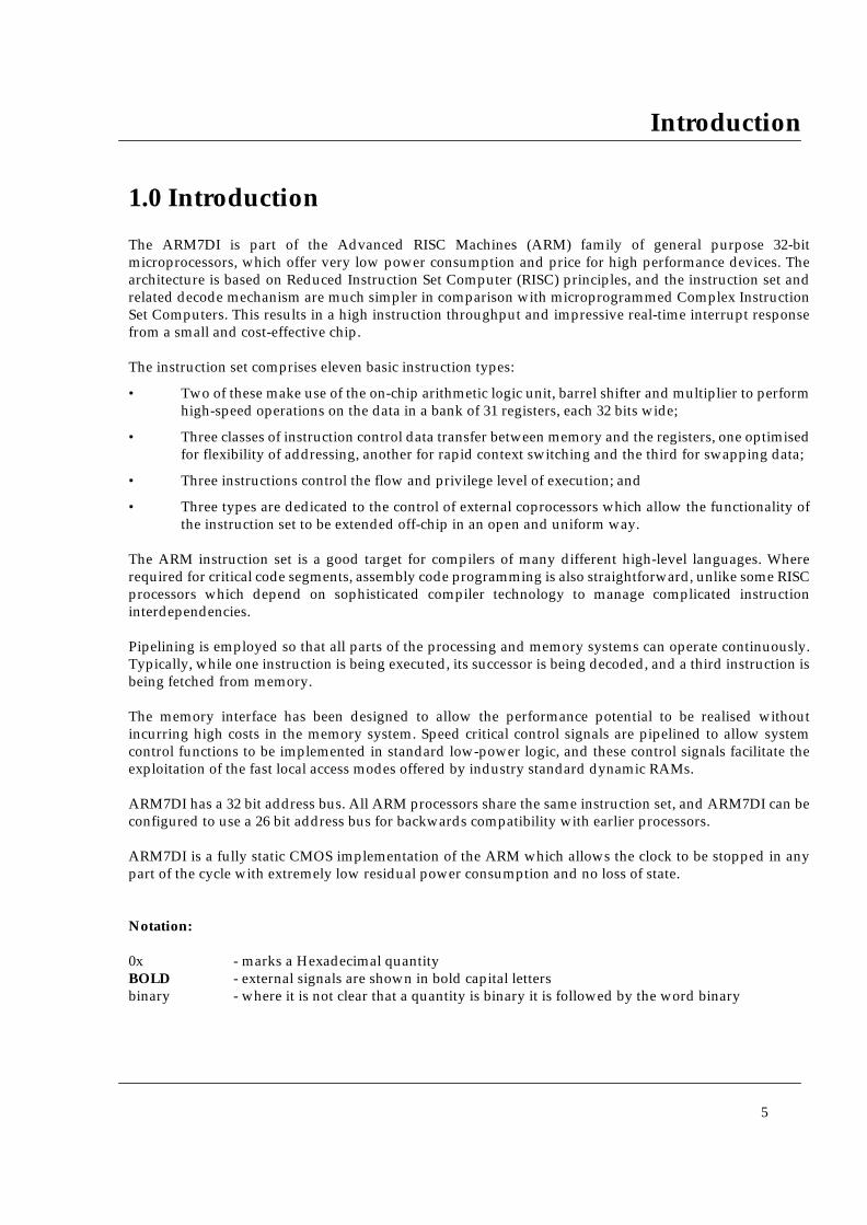
Figure 7: Format of the Program Status Registers (PSRs)
The format of the Program Status Registers is shown in Figure 7: Format of the Program Status Registers(PSRs). The N, Z, C and V bits are the condition code flags. The condition code flags in the CPSR may bechanged as a result of arithmetic and logical operations in the processor and may be tested by allinstructions to determine if the instruction is to be executed.
The I and F bits are the interrupt disable bits. The I bit disables IRQ interrupts when it is set and the F bitdisables FIQ interrupts when it is set. The M0, M1, M2, M3 and M4 bits (M[4:0]) are the mode bits, and thesedetermine the mode in which the processor operates. The interpretation of the mode bits is shown in Table2: The Mode Bits. Not all bit combinations define a valid processor mode. Only those explicitly describedshall be used. The user should be aware that if any illegal value is programmed into the mode bits, M[4:0],the processor will enter an unrecoverable state. If this occurs, reset should be applied.
The bottom 28 bits of a PSR (incorporating I, F and M[4:0]) are known collectively as the control bits. Thesewill change when an exception arises and in addition can be manipulated by software when the processoris in a privileged mode. Unused bits in the PSRs are reserved and their state shall be preserved whenchanging the flag or control bits. Programs shall not rely on specific values from the reserved bits whenchecking the PSR status, since they may read as one or zero in future processors.
M[4:0] Mode Accessible register set
10000 User PC, R14..R0 CPSR
10001 FIQ PC, R14_fiq..R8_fiq, R7..R0 CPSR, SPSR_fiq
10010 IRQ PC, R14_irq..R13_irq, R12..R0 CPSR, SPSR_irq
10011 Supervisor PC, R14_svc..R13_svc, R12..R0 CPSR, SPSR_svc
10111 Abort PC, R14_abt..R13_abt, R12..R0 CPSR, SPSR_abt
11011 Undefined PC, R14_und..R13_und, R12..R0 CPSR, SPSR_und
Table 2: The Mode Bits
0123456782728293031
M0M1M2M3M4.FIVCZN
OverflowCarry / Borrow / ExtendZeroNegative / Less Than
Mode bitsFIQ disableIRQ disable
. ..
flags control

ARM7DI Data Sheet
20
3.4 Exceptions
Exceptions arise whenever there is a need for the normal flow of program execution to be broken, so that(for example) the processor can be diverted to handle an interrupt from a peripheral. The processor statejust prior to handling the exception must be preserved so that the original program can be resumed whenthe exception routine has completed. Many exceptions may arise at the same time.
ARM7DI handles exceptions by making use of the banked registers to save state. The old PC and CPSRcontents are copied into the appropriate R14 and SPSR and the PC and mode bits in the CPSR bits are forcedto a value which depends on the exception. Interrupt disable flags are set where required to preventotherwise unmanageable nestings of exceptions. In the case of a re-entrant interrupt handler, R14 and theSPSR should be saved onto a stack in main memory before re-enabling the interrupt; when transferring theSPSR register to and from a stack, it is important to transfer the whole 32 bit value, and not just the flag orcontrol fields. When multiple exceptions arise simultaneously, a fixed priority determines the order inwhich they are handled. This is listed later in Section 3.4.7: Exception Priorities on page 23.
3.4.1 FIQ
The FIQ (Fast Interrupt reQuest) exception is externally generated by taking the nFIQ input LOW. Thisinput can except either synchronous or asynchronous transitions, depending on the state of the ISYNCinput signal. When ISYNC is LOW, nFIQ (and nIRQ) are considered asynchronous, and a cycle delay forsynchronisation is incurred before the interrupt can affect the processor flow. FIQ is designed to support adata transfer or channel process, and has sufficient private registers to remove the need for register savingin such applications (thus minimising the overhead of context switching). The FIQ exception may bedisabled by setting the F flag in the CPSR (but note that this is not possible from User mode). If the F flag isclear, ARM7DI checks for a LOW level on the output of the FIQ synchroniser at the end of each instruction.
When a FIQ is detected, ARM7DI:
(1) Saves the address of the next instruction to be executed plus 4 in R14_fiq; saves CPSR in SPSR_fiq
(2) Forces M[4:0]=10001 (FIQ mode) and sets the F and I bits in the CPSR
(3) Forces the PC to fetch the next instruction from address 0x1C
To return normally from FIQ, use SUBS PC, R14_fiq,#4 which will restore both the PC (from R14) and theCPSR (from SPSR_fiq) and resume execution of the interrupted code.
3.4.2 IRQ
The IRQ (Interrupt ReQuest) exception is a normal interrupt caused by a LOW level on the nIRQ input. Ithas a lower priority than FIQ, and is masked out when a FIQ sequence is entered. Its effect may be maskedout at any time by setting the I bit in the CPSR (but note that this is not possible from User mode). If the Iflag is clear, ARM7DI checks for a LOW level on the output of the IRQ synchroniser at the end of eachinstruction. Note that nIRQ may also have synchronous or asynchronous timing, depending on the state ofthe ISYNC input. When an IRQ is detected, ARM7DI:

Programmer's Model
21
(1) Saves the address of the next instruction to be executed plus 4 in R14_irq; saves CPSR in SPSR_irq
(2) Forces M[4:0]=10010 (IRQ mode) and sets the I bit in the CPSR
(3) Forces the PC to fetch the next instruction from address 0x18
To return normally from IRQ, use SUBS PC,R14_irq,#4 which will restore both the PC and the CPSR andresume execution of the interrupted code.
3.4.3 Abort
An abort can be signalled by the external ABORT input. ABORT indicates that the current memory accesscannot be completed. For instance, in a virtual memory system the data corresponding to the currentaddress may have been moved out of memory onto a disc, and considerable processor activity may berequired to recover the data before the access can be performed successfully. ARM7DI checks for abortsduring memory access cycles. When successfully aborted ARM7DI will respond in one of two ways:
(1) If the abort occurred during an instruction prefetch (a Prefetch Abort), the prefetched instruction ismarked as invalid but the abort exception does not occur immediately. If the instruction is notexecuted, for example as a result of a branch being taken while it is in the pipeline, no abort willoccur. An abort will take place if the instruction reaches the head of the pipeline and is about to beexecuted.
(2) If the abort occurred during a data access (a Data Abort), the action depends on the instruction type.
(a) Single data transfer instructions (LDR, STR) will write back modified base registers and the Aborthandler must be aware of this.
(b) The swap instruction (SWP) is aborted as though it had not executed, though externally the readaccess may take place.
(c) Block data transfer instructions (LDM, STM) complete, and if write-back is set, the base is updated.If the instruction would normally have overwritten the base with data (i.e. LDM with the base inthe transfer list), this overwriting is prevented. All register overwriting is prevented after the Abortis indicated, which means in particular that R15 (which is always last to be transferred) is preservedin an aborted LDM instruction.
When either a prefetch or data abort occurs, ARM7DI:
(1) Saves the address of the aborted instruction plus 4 (for prefetch aborts) or 8 (for data aborts) inR14_abt; saves CPSR in SPSR_abt.
(2) Forces M[4:0]=10111 (Abort mode) and sets the I bit in the CPSR.
(3) Forces the PC to fetch the next instruction from either address 0x0C (prefetch abort) or address 0x10(data abort).
To return after fixing the reason for the abort, use SUBS PC,R14_abt,#4 (for a prefetch abort) or SUBSPC,R14_abt,#8 (for a data abort). This will restore both the PC and the CPSR and retry the abortedinstruction.

ARM7DI Data Sheet
22
The abort mechanism allows a demand paged virtual memory system to be implemented when suitablememory management software is available. The processor is allowed to generate arbitrary addresses, andwhen the data at an address is unavailable the MMU signals an abort. The processor traps into systemsoftware which must work out the cause of the abort, make the requested data available, and retry theaborted instruction. The application program needs no knowledge of the amount of memory available toit, nor is its state in any way affected by the abort.
3.4.4 Software interrupt
The software interrupt instruction (SWI) is used for getting into Supervisor mode, usually to request aparticular supervisor function. When a SWI is executed, ARM7DI performs the following:
(1) Saves the address of the SWI instruction plus 4 in R14_svc; saves CPSR in SPSR_svc
(2) Forces M[4:0]=10011 (Supervisor mode) and sets the I bit in the CPSR
(3) Forces the PC to fetch the next instruction from address 0x08
To return from a SWI, use MOVS PC,R14_svc. This will restore the PC and CPSR and return to theinstruction following the SWI.
3.4.5 Undefined instruction trap
When the ARM7DI comes across an instruction which it cannot handle (see Chapter 4.0: Instruction Set), itoffers it to any coprocessors which may be present. If a coprocessor can perform this instruction but is busyat that time, ARM7DI will wait until the coprocessor is ready or until an interrupt occurs. If no coprocessorcan handle the instruction then ARM7DI will take the undefined instruction trap.
The trap may be used for software emulation of a coprocessor in a system which does not have thecoprocessor hardware, or for general purpose instruction set extension by software emulation.
When ARM7DI takes the undefined instruction trap it performs the following:
(1) Saves the address of the Undefined or coprocessor instruction plus 4 in R14_und; saves CPSR inSPSR_und.
(2) Forces M[4:0]=11011 (Undefined mode) and sets the I bit in the CPSR
(3) Forces the PC to fetch the next instruction from address 0x04
To return from this trap after emulating the failed instruction, use MOVS PC,R14_und. This will restore theCPSR and return to the instruction following the undefined instruction.

Programmer's Model
23
3.4.6 Vector Summary
These are byte addresses, and will normally contain a branch instruction pointing to the relevant routine.
The FIQ routine might reside at 0x1C onwards, and thereby avoid the need for (and execution time of) abranch instruction.
3.4.7 Exception Priorities
When multiple exceptions arise at the same time, a fixed priority system determines the order in which theywill be handled:
(1) Reset (highest priority)
(2) Data abort
(3) FIQ
(4) IRQ
(5) Prefetch abort
(6) Undefined Instruction, Software interrupt (lowest priority)
Note that not all exceptions can occur at once. Undefined instruction and software interrupt are mutuallyexclusive since they each correspond to particular (non-overlapping) decodings of the current instruction.
If a data abort occurs at the same time as a FIQ, and FIQs are enabled (i.e. the F flag in the CPSR is clear),ARM7DI will enter the data abort handler and then immediately proceed to the FIQ vector. A normal returnfrom FIQ will cause the data abort handler to resume execution. Placing data abort at a higher priority thanFIQ is necessary to ensure that the transfer error does not escape detection; the time for this exception entryshould be added to worst case FIQ latency calculations.
Address Exception Mode on entry
0x00000000 Reset Supervisor
0x00000004 Undefined instruction Undefined
0x00000008 Software interrupt Supervisor
0x0000000C Abort (prefetch) Abort
0x00000010 Abort (data) Abort
0x00000014 -- reserved -- --
0x00000018 IRQ IRQ
0x0000001C FIQ FIQ
Table 3: Vector Summary

ARM7DI Data Sheet
24
3.4.8 Interrupt Latencies
The worst case latency for FIQ, assuming that it is enabled, consists of the longest time the request can taketo pass through the synchroniser (Tsyncmax if asynchronous), plus the time for the longest instruction tocomplete (Tldm, the longest instruction is an LDM which loads all the registers including the PC), plus thetime for the data abort entry (Texc), plus the time for FIQ entry (Tfiq). At the end of this time ARM7DI willbe executing the instruction at 0x1C.
Tsyncmax is 3 processor cycles, Tldm is 20 cycles, Texc is 3 cycles, and Tfiq is 2 cycles. The total time istherefore 28 processor cycles. This is just over 1.4 microseconds in a system which uses a continuous 20MHz processor clock. The maximum IRQ latency calculation is similar, but must allow for the fact that FIQhas higher priority and could delay entry into the IRQ handling routine for an arbitrary length of time. Theminimum latency for FIQ or IRQ consists of the shortest time the request can take through the synchroniser(Tsyncmin) plus Tfiq. This is 4 processor cycles.
3.5 Reset
When the nRESET signal goes LOW, ARM7DI abandons the executing instruction and then continues tofetch instructions from incrementing word addresses.
When nRESET goes HIGH again, ARM7DI does the following:
(1) Overwrites R14_svc and SPSR_svc by copying the current values of the PC and CPSR into them.The value of the saved PC and CPSR is not defined.
(2) Forces M[4:0]=10011 (Supervisor mode) and sets the I and F bits in the CPSR.
(3) Forces the PC to fetch the next instruction from address 0x00

Instruction Set - Summary
25
4.0 Instruction Set
4.1 Instruction Set Summary
A summary of the ARM7DI instruction set is shown in Figure 8: Instruction Set Summary.
Note: some instruction codes are not defined but do not cause the Undefined instruction trap to be taken,for instance a Multiply instruction with bit 6 changed to a 1. These instructions shall not be used,as their action may change in future ARM implementations.
Figure 8: Instruction Set Summary
31 28 27 24 23 20 19 16 15 12 11 8 7 5 4 3 0
Cond 0 0 Opcode
21
S Rn Rd Operand 2Data ProcessingPSR Transfer
Multiply
Single Data Swap
Single Data Transfer
Undefined
Block Data Transfer
Coproc Data Transfer
Branch
Coproc Data Operation
Coproc Register Transfer
Software Interrupt
26 25 22
I
Cond
Cond
Cond
Cond
Cond
Cond
Cond
Cond
Cond
Cond
0 0 0 0 0 0 SA Rd Rn Rs 1 0 0 1 Rm
1 0 0 1 Rm0 0 0 0RdRn0 0 0 1 0 B 0 0
offsetRdRnB W LI P U0 1
0 1 1 XXXXXXXXXXXXXXXXXXXX 1 XXXX
1 0 0 S W LP U Rn Register List
1 0 1 L
1 1 0
offset
1 1 1 0 0 CRm
1 1 1 0 LCP Opc
N W LP U Rn offset CRd CP#
1 1 1 1
CP Opc CRn CRd
CRn Rd
CP#
CP#
CP
CP 1 CRm
ignored by processor
ARM7DI Data Sheet
26
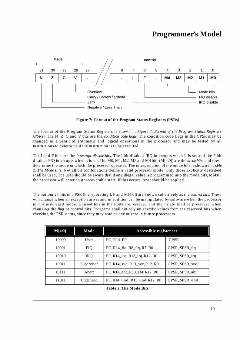
4.2 The Condition Field
Figure 9: Condition Codes
All ARM7DI instructions are conditionally executed, which means that their execution may or may not takeplace depending on the values of the N, Z, C and V flags in the CPSR. The condition encoding is shown inFigure 9: Condition Codes.
If the always (AL) condition is specified, the instruction will be executed irrespective of the flags. The never(NV) class of condition codes shall not be used as they will be redefined in future variants of the ARMarchitecture. If a NOP is required it is suggested that MOV R0,R0 be used. The assembler treats the absenceof a condition code as though always had been specified.
The other condition codes have meanings as detailed in Figure 9: Condition Codes, for instance code 0000(EQual) causes the instruction to be executed only if the Z flag is set. This would correspond to the casewhere a compare (CMP) instruction had found the two operands to be equal. If the two operands weredifferent, the compare instruction would have cleared the Z flag and the instruction will not be executed.
Cond
31 28 27 0
Condition field0000 = EQ - Z set (equal)0001 = NE - Z clear (not equal)0010 = CS - C set (unsigned higher or same)0011 = CC - C clear (unsigned lower)0100 = MI - N set (negative)0101 = PL - N clear (positive or zero)0110 = VS - V set (overflow)0111 = VC - V clear (no overflow)1000 = HI - C set and Z clear (unsigned higher)1001 = LS - C clear or Z set (unsigned lower or same)1010 = GE - N set and V set, or N clear and V clear (greater or equal)1011 = LT - N set and V clear, or N clear and V set (less than)1100 = GT - Z clear, and either N set and V set, or N clear and V clear (greater than)1101 = LE - Z set, or N set and V clear, or N clear and V set (less than or equal)1110 = AL - always1111 = NV - never

Instruction Set - B, BL
27
4.3 Branch and Branch with link (B, BL)
The instruction is only executed if the condition is true. The various conditions are defined at the beginningof this chapter. The instruction encoding is shown in Figure 10: Branch Instructions.
Branch instructions contain a signed 2's complement 24 bit offset. This is shifted left two bits, sign extendedto 32 bits, and added to the PC. The instruction can therefore specify a branch of +/- 32Mbytes. The branchoffset must take account of the prefetch operation, which causes the PC to be 2 words (8 bytes) ahead of thecurrent instruction.
Figure 10: Branch Instructions
Branches beyond +/- 32Mbytes must use an offset or absolute destination which has been previouslyloaded into a register. In this case the PC should be manually saved in R14 if a Branch with Link typeoperation is required.
4.3.1 The link bit
Branch with Link (BL) writes the old PC into the link register (R14) of the current bank. The PC valuewritten into R14 is adjusted to allow for the prefetch, and contains the address of the instruction followingthe branch and link instruction. Note that the CPSR is not saved with the PC.
To return from a routine called by Branch with Link use MOV PC,R14 if the link register is still valid orLDM Rn!,{..PC} if the link register has been saved onto a stack pointed to by Rn.
4.3.2 Instruction Cycle Times
Branch and Branch with Link instructions take 2S + 1N incremental cycles, where S and N are as defined inSection 5.1: Cycle types on page 71.
4.3.3 Assembler syntax
B{L}{cond} <expression>
{L} is used to request the Branch with Link form of the instruction. If absent, R14 will not be affected by theinstruction.
{cond} is a two-character mnemonic as shown in Figure 9: Condition Codes (EQ, NE, VS etc). If absent thenAL (ALways) will be used.
Cond 101 L offset
31 28 27 25 24 23 0
Link bit0 = Branch1 = Branch with Link
Condition field

ARM7DI Data Sheet
28
<expression> is the destination. The assembler calculates the offset.
Items in {} are optional. Items in <> must be present.
4.3.4 Examples
here BAL here ; assembles to 0xEAFFFFFE (note effect of PC offset)B there ; ALways condition used as default
CMP R1,#0 ; compare R1 with zero and branch to fred if R1BEQ fred ; was zero otherwise continue to next instruction
BL sub+ROM ; call subroutine at computed address
ADDS R1,#1 ; add 1 to register 1, setting CPSR flags on theBLCC sub ; result then call subroutine if the C flag is clear,
; which will be the case unless R1 held 0xFFFFFFFF

Instruction Set - Data processing
29
4.4 Data processing
The instruction is only executed if the condition is true, defined at the beginning of this chapter. Theinstruction encoding is shown in Figure 11: Data Processing Instructions.
The instruction produces a result by performing a specified arithmetic or logical operation on one or twooperands. The first operand is always a register (Rn). The second operand may be a shifted register (Rm) ora rotated 8 bit immediate value (Imm) according to the value of the I bit in the instruction. The conditioncodes in the CPSR may be preserved or updated as a result of this instruction, according to the value of theS bit in the instruction. Certain operations (TST, TEQ, CMP, CMN) do not write the result to Rd. They areused only to perform tests and to set the condition codes on the result and always have the S bit set. Theinstructions and their effects are listed in Table 4: ARM Data Processing Instructions.
Figure 11: Data Processing Instructions
Cond 00 I OpCode Rn Rd Operand 2
011121516192021242526272831
Destination register1st operand registerSet condition codes
Operation Code
0 = do not alter condition codes1 = set condition codes
0000 = AND - Rd:= Op1 AND Op2
0010 = SUB - Rd:= Op1 - Op20011 = RSB - Rd:= Op2 - Op10100 = ADD - Rd:= Op1 + Op20101 = ADC - Rd:= Op1 + Op2 + C0110 = SBC - Rd:= Op1 - Op2 + C0111 = RSC - Rd:= Op2 - Op1 + C1000 = TST - set condition codes on Op1 AND Op21001 = TEQ - set condition codes on Op1 EOR Op21010 = CMP - set condition codes on Op1 - Op21011 = CMN - set condition codes on Op1 + Op21100 = ORR - Rd:= Op1 OR Op21101 = MOV - Rd:= Op21110 = BIC - Rd:= Op1 AND NOT Op21111 = MVN - Rd:= NOT Op2
Immediate Operand0 = operand 2 is a register
1 = operand 2 is an immediate value
Shift Rm
Rotate
S
Unsigned 8 bit immediate value
2nd operand registershift applied to Rm
shift applied to Imm
Imm
Condition field
11 8 7 0
03411
0001 = EOR - Rd:= Op1 EOR Op2
- 1- 1
ARM7DI Data Sheet
30
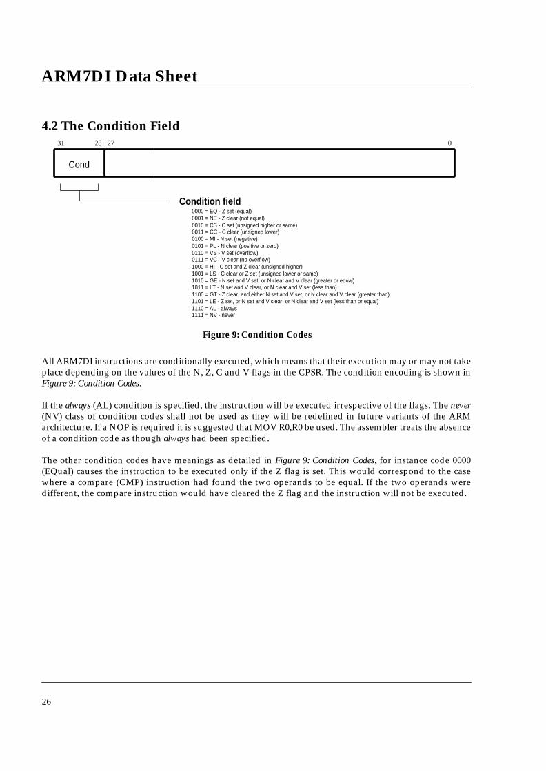
4.4.1 CPSR flags
The data processing operations may be classified as logical or arithmetic. The logical operations (AND,EOR, TST, TEQ, ORR, MOV, BIC, MVN) perform the logical action on all corresponding bits of the operandor operands to produce the result. If the S bit is set (and Rd is not R15, see below) the V flag in the CPSR willbe unaffected, the C flag will be set to the carry out from the barrel shifter (or preserved when the shiftoperation is LSL #0), the Z flag will be set if and only if the result is all zeros, and the N flag will be set tothe logical value of bit 31 of the result.
The arithmetic operations (SUB, RSB, ADD, ADC, SBC, RSC, CMP, CMN) treat each operand as a 32 bitinteger (either unsigned or 2's complement signed, the two are equivalent). If the S bit is set (and Rd is notR15) the V flag in the CPSR will be set if an overflow occurs into bit 31 of the result; this may be ignored ifthe operands were considered unsigned, but warns of a possible error if the operands were 2's complementsigned. The C flag will be set to the carry out of bit 31 of the ALU, the Z flag will be set if and only if theresult was zero, and the N flag will be set to the value of bit 31 of the result (indicating a negative result ifthe operands are considered to be 2's complement signed).
AssemblerMnemonic
OpCode Action
AND 0000 operand1 AND operand2
EOR 0001 operand1 EOR operand2
SUB 0010 operand1 - operand2
RSB 0011 operand2 - operand1
ADD 0100 operand1 + operand2
ADC 0101 operand1 + operand2 + carry
SBC 0110 operand1 - operand2 + carry - 1
RSC 0111 operand2 - operand1 + carry - 1
TST 1000 as AND, but result is not written
TEQ 1001 as EOR, but result is not written
CMP 1010 as SUB, but result is not written
CMN 1011 as ADD, but result is not written
ORR 1100 operand1 OR operand2
MOV 1101 operand2 (operand1 is ignored)
BIC 1110 operand1 AND NOT operand2 (Bit clear)
MVN 1111 NOT operand2 (operand1 is ignored)
Table 4: ARM Data Processing Instructions

Instruction Set - Shifts
31
4.4.2 Shifts
When the second operand is specified to be a shifted register, the operation of the barrel shifter is controlledby the Shift field in the instruction. This field indicates the type of shift to be performed (logical left or right,arithmetic right or rotate right). The amount by which the register should be shifted may be contained inan immediate field in the instruction, or in the bottom byte of another register (other than R15). Theencoding for the different shift types is shown in Figure 12: ARM Shift Operations.
Figure 12: ARM Shift Operations
Instruction specified shift amount
When the shift amount is specified in the instruction, it is contained in a 5 bit field which may take any valuefrom 0 to 31. A logical shift left (LSL) takes the contents of Rm and moves each bit by the specified amountto a more significant position. The least significant bits of the result are filled with zeros, and the high bitsof Rm which do not map into the result are discarded, except that the least significant discarded bit becomesthe shifter carry output which may be latched into the C bit of the CPSR when the ALU operation is in thelogical class (see above). For example, the effect of LSL #5 is shown in Figure 13: Logical Shift Left.
Figure 13: Logical Shift Left
Note that LSL #0 is a special case, where the shifter carry out is the old value of the CPSR C flag. Thecontents of Rm are used directly as the second operand.
A logical shift right (LSR) is similar, but the contents of Rm are moved to less significant positions in theresult. LSR #5 has the effect shown in Figure 14: Logical Shift Right.
0 0 1Rs
11 8 7 6 5 411 7 6 5 4
Shift type
Shift amount5 bit unsigned integer
00 = logical left01 = logical right10 = arithmetic right11 = rotate right
Shift type
Shift register
00 = logical left01 = logical right10 = arithmetic right11 = rotate right
Shift amount specified inbottom byte of Rs
0 0 0 0 0
contents of Rm
value of operand 2
31 27 26 0
carry out

ARM7DI Data Sheet
32
Figure 14: Logical Shift Right
The form of the shift field which might be expected to correspond to LSR #0 is used to encode LSR #32,which has a zero result with bit 31 of Rm as the carry output. Logical shift right zero is redundant as it isthe same as logical shift left zero, so the assembler will convert LSR #0 (and ASR #0 and ROR #0) into LSL#0, and allow LSR #32 to be specified.
An arithmetic shift right (ASR) is similar to logical shift right, except that the high bits are filled with bit 31of Rm instead of zeros. This preserves the sign in 2's complement notation. For example, ASR #5 is shownin Figure 15: Arithmetic Shift Right.
Figure 15: Arithmetic Shift Right
The form of the shift field which might be expected to give ASR #0 is used to encode ASR #32. Bit 31 of Rmis again used as the carry output, and each bit of operand 2 is also equal to bit 31 of Rm. The result istherefore all ones or all zeros, according to the value of bit 31 of Rm.
Rotate right (ROR) operations reuse the bits which 'overshoot' in a logical shift right operation byreintroducing them at the high end of the result, in place of the zeros used to fill the high end in logical rightoperations. For example, ROR #5 is shown in Figure 16: Rotate Right.
contents of Rm
value of operand 2
31 0
carry out
0 0 0 0 0
5 4
contents of Rm
value of operand 2
31 0
carry out
5 430

Instruction Set - Shifts
33
Figure 16: Rotate Right
The form of the shift field which might be expected to give ROR #0 is used to encode a special function ofthe barrel shifter, rotate right extended (RRX). This is a rotate right by one bit position of the 33 bit quantityformed by appending the CPSR C flag to the most significant end of the contents of Rm as shown in Figure17: Rotate Right Extended.
Figure 17: Rotate Right Extended
Register specified shift amount
Only the least significant byte of the contents of Rs is used to determine the shift amount. Rs can be anygeneral register other than R15.
If this byte is zero, the unchanged contents of Rm will be used as the second operand, and the old value ofthe CPSR C flag will be passed on as the shifter carry output.
If the byte has a value between 1 and 31, the shifted result will exactly match that of an instruction specifiedshift with the same value and shift operation.
If the value in the byte is 32 or more, the result will be a logical extension of the shift described above:
(1) LSL by 32 has result zero, carry out equal to bit 0 of Rm.
(2) LSL by more than 32 has result zero, carry out zero.
(3) LSR by 32 has result zero, carry out equal to bit 31 of Rm.
(4) LSR by more than 32 has result zero, carry out zero.
(5) ASR by 32 or more has result filled with and carry out equal to bit 31 of Rm.
contents of Rm
value of operand 2
31 0
carry out
5 4
contents of Rm
value of operand 2
31 0
carryout
1
Cin
ARM7DI Data Sheet
34
(6) ROR by 32 has result equal to Rm, carry out equal to bit 31 of Rm.
(7) ROR by n where n is greater than 32 will give the same result and carry out as ROR by n-32;therefore repeatedly subtract 32 from n until the amount is in the range 1 to 32 and see above.
Note that the zero in bit 7 of an instruction with a register controlled shift is compulsory; a one in this bitwill cause the instruction to be a multiply or undefined instruction.
4.4.3 Immediate operand rotates
The immediate operand rotate field is a 4 bit unsigned integer which specifies a shift operation on the 8 bitimmediate value. This value is zero extended to 32 bits, and then subject to a rotate right by twice the valuein the rotate field. This enables many common constants to be generated, for example all powers of 2.
4.4.4 Writing to R15
When Rd is a register other than R15, the condition code flags in the CPSR may be updated from the ALUflags as described above.
When Rd is R15 and the S flag in the instruction is not set the result of the operation is placed in R15 andthe CPSR is unaffected.
When Rd is R15 and the S flag is set the result of the operation is placed in R15 and the SPSR correspondingto the current mode is moved to the CPSR. This allows state changes which atomically restore both PC andCPSR. This form of instruction shall not be used in User mode.
4.4.5 Using R15 as an operand
If R15 (the PC) is used as an operand in a data processing instruction the register is used directly.
The PC value will be the address of the instruction, plus 8 or 12 bytes due to instruction prefetching. If theshift amount is specified in the instruction, the PC will be 8 bytes ahead. If a register is used to specify theshift amount the PC will be 12 bytes ahead.
4.4.6 TEQ, TST, CMP & CMN opcodes
These instructions do not write the result of their operation but do set flags in the CPSR. An assembler shallalways set the S flag for these instructions even if it is not specified in the mnemonic.
The TEQP form of the instruction used in earlier processors shall not be used in the 32 bit modes, the PSRtransfer operations should be used instead. If used in these modes, its effect is to move SPSR_<mode> toCPSR if the processor is in a privileged mode and to do nothing if in User mode.
4.4.7 Instruction Cycle Times
Data Processing instructions vary in the number of incremental cycles taken as follows:
Normal Data Processing 1S
Data Processing with register specified shift 1S + 1I

Instruction Set - TEQ, TST, CMP & CMN
35
Data Processing with PC written 2S + 1NData Processing with register specified shift and PCwritten 2S + 1N + 1I
S, N and I are as defined in Section 5.1: Cycle types on page 71.
4.4.8 Assembler syntax
(1) MOV,MVN - single operand instructions
<opcode>{cond}{S} Rd,<Op2>
(2) CMP,CMN,TEQ,TST - instructions which do not produce a result.
<opcode>{cond} Rn,<Op2>
(3) AND,EOR,SUB,RSB,ADD,ADC,SBC,RSC,ORR,BIC
<opcode>{cond}{S} Rd,Rn,<Op2>
where <Op2> is Rm{,<shift>} or,<#expression>
{cond} - two-character condition mnemonic, see Figure 9: Condition Codes
{S} - set condition codes if S present (implied for CMP, CMN, TEQ, TST).
Rd, Rn and Rm are expressions evaluating to a register number.
If <#expression> is used, the assembler will attempt to generate a shifted immediate 8-bit field to match theexpression. If this is impossible, it will give an error.
<shift> is <shiftname> <register> or <shiftname> #expression, or RRX (rotate right one bit with extend).
<shiftname>s are: ASL, LSL, LSR, ASR, ROR. (ASL is a synonym for LSL, they assemble to the same code.)
4.4.9 Examples
ADDEQ R2,R4,R5 ; if the Z flag is set make R2:=R4+R5
TEQS R4,#3 ; test R4 for equality with 3; (the S is in fact redundant as the; assembler inserts it automatically)
SUB R4,R5,R7,LSR R2 ; logical right shift R7 by the number in; the bottom byte of R2, subtract result; from R5, and put the answer into R4
MOV PC,R14 ; return from subroutine
MOVS PC,R14 ; return from exception and restore CPSR from SPSR_mode

ARM7DI Data Sheet
36
4.5 PSR Transfer (MRS, MSR)
The instruction is only executed if the condition is true. The various conditions are defined at the beginningof this chapter.
The MRS and MSR instructions are formed from a subset of the Data Processing operations and areimplemented using the TEQ, TST, CMN and CMP instructions without the S flag set. The encoding isshown in Figure 18: PSR Transfer.
These instructions allow access to the CPSR and SPSR registers. The MRS instruction allows the contents ofthe CPSR or SPSR_<mode> to be moved to a general register. The MSR instruction allows the contents of ageneral register to be moved to the CPSR or SPSR_<mode> register.
The MSR instruction also allows an immediate value or register contents to be transferred to the conditioncode flags (N,Z,C and V) of CPSR or SPSR_<mode> without affecting the control bits. In this case, the topfour bits of the specified register contents or 32 bit immediate value are written to the top four bits of therelevant PSR.
4.5.1 Operand restrictions
In User mode, the control bits of the CPSR are protected from change, so only the condition code flags ofthe CPSR can be changed. In other (privileged) modes the entire CPSR can be changed.
The SPSR register which is accessed depends on the mode at the time of execution. For example, onlySPSR_fiq is accessible when the processor is in FIQ mode.
R15 shall not be specified as the source or destination register.
A further restriction is that no attempt shall be made to access an SPSR in User mode, since no such registerexists.

Instruction Set - MRS, MSR
37
Figure 18: PSR Transfer
Cond
01112151621272831
Condition field
P
2223
0 = CPSR1 = SPSR_<current mode>
00010 000000000000s 001111 Rd
Destination register
Source PSR
Condition field
MRS
021272831 2223
MSR
RmPdCond 00010
4 3
Condition field
272831 2223
MSR
PdCond
1010011111 00000000
12 11
Source register
21 12
101000111100 I 10
011
Source operand
Immediate Operand
Rm
Rotate
Unsigned 8 bit immediate value
shift applied to Imm
Imm
11 8 7 0
03411
Destination PSR0 = CPSR1 = SPSR_<current mode>
Destination PSR0 = CPSR1 = SPSR_<current mode>
0 = Source operand is a register
1 = Source operand is an immediate value
00000000
Source register
(transfer PSR contents to a register)
(transfer register contents to PSR)
(transfer register contents or immediate value to PSR flag bits only)

ARM7DI Data Sheet
38
4.5.2 Reserved bits
Only eleven bits of the PSR are defined in ARM7DI (N,Z,C,V,I,F & M[4:0]); the remaining bits (=PSR[27:8,5]) are reserved for use in future versions of the processor. To ensure the maximum compatibilitybetween ARM7DI programs and future processors, the following rules should be observed:
(1) The reserved bits shall be preserved when changing the value in a PSR.
(2) Programs shall not rely on specific values from the reserved bits when checking the PSR status,since they may read as one or zero in future processors.
A read-modify-write strategy should therefore be used when altering the control bits of any PSR register;this involves transferring the appropriate PSR register to a general register using the MRS instruction,changing only the relevant bits and then transferring the modified value back to the PSR register using theMSR instruction.
e.g. The following sequence performs a mode change:
MRS R0,CPSR ; take a copy of the CPSRBIC R0,R0,#0x1F ; clear the mode bitsORR R0,R0,#new_mode ; select new modeMSR CPSR,R0 ; write back the modified CPSR
When the aim is simply to change the condition code flags in a PSR, a value can be written directly to theflag bits without disturbing the control bits. e.g. The following instruction sets the N,Z,C & V flags:
MSR CPSR_flg,#0xF0000000 ; set all the flags regardless of; their previous state (does not; affect any control bits)
No attempt shall be made to write an 8 bit immediate value into the whole PSR since such an operationcannot preserve the reserved bits.
4.5.3 Instruction Cycle Times
PSR Transfers take 1S incremental cycles, where S is as defined in Section 5.1: Cycle types on page 71.
4.5.4 Assembler syntax
(1) MRS - transfer PSR contents to a register
MRS{cond} Rd,<psr>
(2) MSR - transfer register contents to PSR
MSR{cond} <psr>,Rm
(3) MSR - transfer register contents to PSR flag bits only
MSR{cond} <psrf>,Rm
The most significant four bits of the register contents are written to the N,Z,C & V flags respectively.

Instruction Set - MRS, MSR
39
(4) MSR - transfer immediate value to PSR flag bits only
MSR{cond} <psrf>,<#expression>
The expression should symbolise a 32 bit value of which the most significant four bits are writtento the N,Z,C & V flags respectively.
{cond} - two-character condition mnemonic, see Figure 9: Condition Codes
Rd and Rm are expressions evaluating to a register number other than R15
<psr> is CPSR, CPSR_all, SPSR or SPSR_all. (CPSR and CPSR_all are synonyms as are SPSR and SPSR_all)
<psrf> is CPSR_flg or SPSR_flg
Where <#expression> is used, the assembler will attempt to generate a shifted immediate 8-bit field tomatch the expression. If this is impossible, it will give an error.
4.5.5 Examples
In User mode the instructions behave as follows:
MSR CPSR_all,Rm ; CPSR[31:28] <- Rm[31:28]MSR CPSR_flg,Rm ; CPSR[31:28] <- Rm[31:28]
MSR CPSR_flg,#0xA0000000 ; CPSR[31:28] <- 0xA; (i.e. set N,C; clear Z,V)
MRS Rd,CPSR ; Rd[31:0] <- CPSR[31:0]
In privileged modes the instructions behave as follows:
MSR CPSR_all,Rm ; CPSR[31:0] <- Rm[31:0]MSR CPSR_flg,Rm ; CPSR[31:28] <- Rm[31:28]
MSR CPSR_flg,#0x50000000 ; CPSR[31:28] <- 0x5; (i.e. set Z,V; clear N,C)
MRS Rd,CPSR ; Rd[31:0] <- CPSR[31:0]
MSR SPSR_all,Rm ; SPSR_<mode>[31:0] <- Rm[31:0]MSR SPSR_flg,Rm ; SPSR_<mode>[31:28] <- Rm[31:28]
MSR SPSR_flg,#0xC0000000 ; SPSR_<mode>[31:28] <- 0xC; (i.e. set N,Z; clear C,V)
MRS Rd,SPSR ; Rd[31:0] <- SPSR_<mode>[31:0]

ARM7DI Data Sheet
40
4.6 Multiply and Multiply-Accumulate (MUL, MLA)
The instruction is only executed if the condition is true. The various conditions are defined at the beginningof this chapter. The instruction encoding is shown in Figure 19: Multiply Instructions.
The multiply and multiply-accumulate instructions use a 2 bit Booth's algorithm to perform integermultiplication. They give the least significant 32 bits of the product of two 32 bit operands, and may be usedto synthesize higher precision multiplications.
Figure 19: Multiply Instructions
The multiply form of the instruction gives Rd:=Rm*Rs. Rn is ignored, and should be set to zero forcompatibility with possible future upgrades to the instruction set.
The multiply-accumulate form gives Rd:=Rm*Rs+Rn, which can save an explicit ADD instruction in somecircumstances.
Both forms of the instruction work on operands which may be considered as signed (2’s complement) orunsigned integers.
Cond 0 0 0 0 0 0 A S Rd Rn Rs 1 0 0 1 Rm
034781112151619202122272831
Operand registersDestination registerSet condition code
Accumulate
0 = do not alter condition codes1 = set condition codes
0 = multiply only1 = multiply and accumulate
Condition Field

Instruction Set - MUL, MLA
41
4.6.1 Operand Restrictions
Due to the way multiplication was implemented, certain combinations of operand registers should beavoided. (The assembler will issue a warning if these restrictions are overlooked.)
The destination register (Rd) should not be the same as the operand register (Rm), as Rd is used to holdintermediate values and Rm is used repeatedly during multiply. A MUL will give a zero result if RM=Rd,and an MLA will give a meaningless result. R15 shall not be used as an operand or as the destinationregister.
All other register combinations will give correct results, and Rd, Rn and Rs may use the same register whenrequired.
4.6.2 CPSR flags
Setting the CPSR flags is optional, and is controlled by the S bit in the instruction. The N (Negative) and Z(Zero) flags are set correctly on the result (N is made equal to bit 31 of the result, and Z is set if and only ifthe result is zero). The C (Carry) flag is set to a meaningless value and the V (oVerflow) flag is unaffected.
4.6.3 Instruction Cycle Times
The Multiply instructions take 1S + mI cycles to execute, where S and I are as defined in Section 5.1: Cycletypes on page 71.
m is the number of cycles required by the multiply algorithm, which is determined by the contents ofRs. Multiplication by any number between 2^(2m-3) and 2^(2m-1)-1 takes 1S+mI cycles for1<m>16. Multiplication by 0 or 1 takes 1S+1I cycles, and multiplication by any number greater thanor equal to 2^(29) takes 1S+16I cycles. The maximum time for any multiply is thus 1S+16I cycles.
4.6.4 Assembler syntax
MUL{cond}{S} Rd,Rm,Rs
MLA{cond}{S} Rd,Rm,Rs,Rn
{cond} - two-character condition mnemonic, see Figure 9: Condition Codes
{S} - set condition codes if S present
Rd, Rm, Rs and Rn are expressions evaluating to a register number other than R15.
4.6.5 Examples
MUL R1,R2,R3 ; R1:=R2*R3MLAEQS R1,R2,R3,R4 ; conditionally R1:=R2*R3+R4,
; setting condition codes

ARM7DI Data Sheet
42
4.7 Single data transfer (LDR, STR)
The instruction is only executed if the condition is true. The various conditions are defined at the beginningof this chapter. The instruction encoding is shown in Figure 20: Single Data Transfer Instructions.
The single data transfer instructions are used to load or store single bytes or words of data. The memoryaddress used in the transfer is calculated by adding an offset to or subtracting an offset from a base register.The result of this calculation may be written back into the base register if `auto-indexing' is required.
Figure 20: Single Data Transfer Instructions
Cond I Rn Rd
011121516192021242526272831
01 P U B W L Offset
2223
011
Source/Destination registerBase registerLoad/Store bit
0 = Store to memory1 = Load from memory
Write-back bit
Byte/Word bit
0 = no write-back1 = write address into base
0 = transfer word quantity1 = transfer byte quantity
Up/Down bit
Pre/Post indexing bit
0 = offset is an immediate valueImmediate offset
Immediate offset
Unsigned 12 bit immediate offset1 = offset is a register
11 0
shift applied to Rm
34
Condition field
0 = down; subtract offset from base1 = up; add offset to base
0 = post; add offset after transfer1 = pre; add offset before transfer
Offset register
Shift Rm

Instruction Set - LDR, STR
43
4.7.1 Offsets and auto-indexing
The offset from the base may be either a 12 bit unsigned binary immediate value in the instruction, or asecond register (possibly shifted in some way). The offset may be added to (U=1) or subtracted from (U=0)the base register Rn. The offset modification may be performed either before (pre-indexed, P=1) or after(post-indexed, P=0) the base is used as the transfer address.
The W bit gives optional auto increment and decrement addressing modes. The modified base value maybe written back into the base (W=1), or the old base value may be kept (W=0). In the case of post-indexedaddressing, the write back bit is redundant and is always set to zero, since the old base value can be retainedby setting the offset to zero. Therefore post-indexed data transfers always write back the modified base. Theonly use of the W bit in a post-indexed data transfer is in privileged mode code, where setting the W bitforces non-privileged mode for the transfer, allowing the operating system to generate a user address in asystem where the memory management hardware makes suitable use of this hardware.
4.7.2 Shifted register offset
The 8 shift control bits are described in the data processing instructions section. However, the registerspecified shift amounts are not available in this instruction class. See 4.4.2 Shifts.
4.7.3 Bytes and words
This instruction class may be used to transfer a byte (B=1) or a word (B=0) between an ARM7DI registerand memory.
The action of LDR(B) and STR(B) instructions is influenced by the BIGEND control signal. The two possibleconfigurations are described below.
Little Endian Configuration
A byte load (LDRB) expects the data on data bus inputs 7 through 0 if the supplied address is on a wordboundary, on data bus inputs 15 through 8 if it is a word address plus one byte, and so on. The selected byteis placed in the bottom 8 bits of the destination register, and the remaining bits of the register are filled withzeros. Please see Figure 4: Little Endian addresses of bytes within words.
A byte store (STRB) repeats the bottom 8 bits of the source register four times across data bus outputs 31through 0. The external memory system should activate the appropriate byte subsystem to store the data.
A word load (LDR) will normally use a word aligned address. However, an address offset from a wordboundary will cause the data to be rotated into the register so that the addressed byte occupies bits 0 to 7.This means that half-words accessed at offsets 0 and 2 from the word boundary will be correctly loaded intobits 0 through 15 of the register. Two shift operations are then required to clear or to sign extend the upper16 bits. This is illustrated in Figure 21: Little Endian Offset Addressing.

ARM7DI Data Sheet
44
Figure 21: Little Endian Offset Addressing
A word store (STR) should generate a word aligned address. The word presented to the data bus is notaffected if the address is not word aligned. That is, bit 31 of the register being stored always appears on databus output 31.
Big Endian Configuration
A byte load (LDRB) expects the data on data bus inputs 31 through 24 if the supplied address is on a wordboundary, on data bus inputs 23 through 16 if it is a word address plus one byte, and so on. The selectedbyte is placed in the bottom 8 bits of the destination register and the remaining bits of the register are filledwith zeros. Please see Figure 5: Big Endian addresses of bytes within words.
A byte store (STRB) repeats the bottom 8 bits of the source register four times across data bus outputs 31through 0. The external memory system should activate the appropriate byte subsystem to store the data.
A word load (LDR) should generate a word aligned address. An address offset of 0 or 2 from a wordboundary will cause the data to be rotated into the register so that the addressed byte occupies bits 31through 24. This means that half-words accessed at these offsets will be correctly loaded into bits 16 through31 of the register. A shift operation is then required to move (and optionally sign extend) the data into thebottom 16 bits. An address offset of 1 or 3 from a word boundary will cause the data to be rotated into theregister so that the addressed byte occupies bits 15 through 8.
A
B
C
D
memory
A+3
A+2
A+1
A
24
16
8
0
A
B
C
D
register
24
16
8
0
LDR from word aligned address
A
B
C
D
A+3
A+2
A+1
A
24
16
8
0
A
B
C
D
24
16
8
0
LDR from address offset by 2
Instruction Set - LDR, STR
45
A word store (STR) should generate a word aligned address. The word presented to the data bus is notaffected if the address is not word aligned. That is, bit 31 of the register being stored always appears on databus output 31.
4.7.4 Use of R15
Write-back shall not be specified if R15 is specified as the base register (Rn). When using R15 as the baseregister you must remember it contains an address 8 bytes on from the address of the current instruction.
R15 shall not be specified as the register offset (Rm).
When R15 is the source register (Rd) of a register store (STR) instruction, the stored value will be addressof the instruction plus 12.
4.7.5 Restriction on the use of base register
When configured for late aborts, the following example code is difficult to unwind as the base register, Rn,gets updated before the abort handler starts. Sometimes it may be impossible to calculate the initial value.
For example:
LDR R0,[R1],R1
Therefore a post-indexed LDR|STR where Rm is the same register as Rn shall not be used.
4.7.6 Data Aborts
A transfer to or from a legal address may cause problems for a memory management system. For instance,in a system which uses virtual memory the required data may be absent from main memory. The memorymanager can signal a problem by taking the processor ABORT input HIGH whereupon the Data Abort trapwill be taken. It is up to the system software to resolve the cause of the problem, then the instruction can berestarted and the original program continued.
4.7.7 Instruction Cycle Times
Normal LDR instructions take 1S + 1N + 1I and LDR PC take 2S + 2N +1I incremental cycles, where S,Nand I are as defined in Section 5.1: Cycle types on page 71.
STR instructions take 2N incremental cycles to execute.
4.7.8 Assembler syntax
<LDR|STR>{cond}{B}{T} Rd,<Address>
LDR - load from memory into a register
STR - store from a register into memory
{cond} - two-character condition mnemonic, see Figure 9: Condition Codes
ARM7DI Data Sheet
46
{B} - if B is present then byte transfer, otherwise word transfer
{T} - if T is present the W bit will be set in a post-indexed instruction, forcing non-privileged mode for thetransfer cycle. T is not allowed when a pre-indexed addressing mode is specified or implied.
Rd is an expression evaluating to a valid register number.
<Address> can be:
(i) An expression which generates an address:
<expression>
The assembler will attempt to generate an instruction using the PC as a base and a correctedimmediate offset to address the location given by evaluating the expression. This will be a PCrelative, pre-indexed address. If the address is out of range, an error will be generated.
(ii) A pre-indexed addressing specification:
[Rn] offset of zero
[Rn,<#expression>]{!} offset of <expression> bytes
[Rn,{+/-}Rm{,<shift>}]{!} offset of +/- contents of index register, shifted by <shift>
(iii) A post-indexed addressing specification:
[Rn],<#expression> offset of <expression> bytes
[Rn],{+/-}Rm{,<shift>} offset of +/- contents of index register, shifted as by <shift>.
Rn and Rm are expressions evaluating to a register number. If Rn is R15 then the assembler will subtract 8from the offset value to allow for ARM7DI pipelining. In this case base write-back shall not be specified.
<shift> is a general shift operation (see section on data processing instructions) but note that the shiftamount may not be specified by a register.
{!} writes back the base register (set the W bit) if ! is present.
4.7.9 Examples
STR R1,[R2,R4]! ; store R1 at R2+R4 (both of which are; registers) and write back address to R2
STR R1,[R2],R4 ; store R1 at R2 and write back; R2+R4 to R2
LDR R1,[R2,#16] ; load R1 from contents of R2+16; Don't write back
LDR R1,[R2,R3,LSL#2] ; load R1 from contents of R2+R3*4

Instruction Set - LDR, STR
47
LDREQB R1,[R6,#5] ; conditionally load byte at R6+5 into; R1 bits 0 to 7, filling bits 8 to 31; with zeros
STR R1,PLACE ; generate PC relative offset to address• ; PLACE•
PLACE

ARM7DI Data Sheet
48
4.8 Block Data Transfer (LDM, STM)
The instruction is only executed if the condition is true. The various conditions are defined at the beginningof this chapter. The instruction encoding is shown in Figure 22: Block Data Transfer Instructions.
Block data transfer instructions are used to load (LDM) or store (STM) any subset of the currently visibleregisters. They support all possible stacking modes, maintaining full or empty stacks which can grow up ordown memory, and are very efficient instructions for saving or restoring context, or for moving large blocksof data around main memory.
4.8.1 The Register List
The instruction can cause the transfer of any registers in the current bank (and non-user mode programscan also transfer to and from the user bank, see below). The register list is a 16 bit field in the instruction,with each bit corresponding to a register. A 1 in bit 0 of the register field will cause R0 to be transferred, a0 will cause it not to be transferred; similarly bit 1 controls the transfer of R1, and so on.
Any subset of the registers, or all the registers, may be specified. The only restriction is that the register listshould not be empty.
Whenever R15 is stored to memory the stored value is the address of the STM instruction plus 12.
Figure 22: Block Data Transfer Instructions
4.8.2 Addressing Modes
The transfer addresses are determined by the contents of the base register (Rn), the pre/post bit (P) and theup/down bit (U). The registers are transferred in the order lowest to highest, so R15 (if in the list) willalways be transferred last. The lowest register also gets transferred to/from the lowest memory address. Byway of illustration, consider the transfer of R1, R5 and R7 in the case where Rn=0x1000 and write back of
Cond Rn
015161920212425272831
P U W L
2223
100 S Register list
Base registerLoad/Store bit
0 = Store to memory1 = Load from memory
Write-back bit0 = no write-back1 = write address into base
Up/Down bit
Pre/Post indexing bit
0 = down; subtract offset from base1 = up; add offset to base
0 = post; add offset after transfer1 = pre; add offset before transfer
PSR & force user bit0 = do not load PSR or force user mode1 = load PSR or force user mode
Condition field

Instruction Set - LDM, STM
49
the modified base is required (W=1). Figure 23: Post-increment addressing, Figure 24: Pre-increment addressing,Figure 25: Post-decrement addressing and Figure 26: Pre-decrement addressing show the sequence of registertransfers, the addresses used, and the value of Rn after the instruction has completed.
In all cases, had write back of the modified base not been required (W=0), Rn would have retained its initialvalue of 0x1000 unless it was also in the transfer list of a load multiple register instruction, when it wouldhave been overwritten with the loaded value.
4.8.3 Address Alignment
The address should normally be a word aligned quantity and non-word aligned addresses do not affect theinstruction. However, the bottom 2 bits of the address will appear on A[1:0] and might be interpreted bythe memory system.
Figure 23: Post-increment addressing
0x100C
0x1000
0x0FF4
Rn
1
0x100C
0x1000
0x0FF4
2
R1
0x100C
0x1000
0x0FF4
3
0x100C
0x1000
0x0FF4
4
R1
R7
R5
R1
R5
Rn

ARM7DI Data Sheet
50
Figure 24: Pre-increment addressing
Figure 25: Post-decrement addressing
0x100C
0x1000
0x0FF4
Rn
1
0x100C
0x1000
0x0FF4
2
R1
0x100C
0x1000
0x0FF4
3
0x100C
0x1000
0x0FF4
4
R1
R7
R5
R1
R5
Rn
0x100C
0x1000
0x0FF4
Rn
1
0x100C
0x1000
0x0FF4
2
R1
0x100C
0x1000
0x0FF4
3
0x100C
0x1000
0x0FF4
4
R1
R7
R5
R1
R5
Rn

Instruction Set - LDM, STM
51
Figure 26: Pre-decrement addressing
4.8.4 Use of the S bit
When the S bit is set in a LDM/STM instruction its meaning depends on whether or not R15 is in the transferlist and on the type of instruction. The S bit should only be set if the instruction is to execute in a privilegedmode.
LDM with R15 in transfer list and S bit set (Mode changes)
If the instruction is a LDM then SPSR_<mode> is transferred to CPSR at the same time as R15 is loaded.
STM with R15 in transfer list and S bit set (User bank transfer)
The registers transferred are taken from the User bank rather than the bank corresponding to the currentmode. This is useful for saving the user state on process switches. Base write-back shall not be used whenthis mechanism is employed.
R15 not in list and S bit set (User bank transfer)
For both LDM and STM instructions, the User bank registers are transferred rather than the register bankcorresponding to the current mode. This is useful for saving the user state on process switches. Base write-back shall not be used when this mechanism is employed.
When the instruction is LDM, care must be taken not to read from a banked register during the followingcycle (inserting a dummy instruction such as MOV R0, R0 after the LDM will ensure safety).
0x100C
0x1000
0x0FF4
Rn
1
0x100C
0x1000
0x0FF4
2
R1
0x100C
0x1000
0x0FF4
3
0x100C
0x1000
0x0FF4
4
R1
R7
R5
R1
R5
Rn

ARM7DI Data Sheet
52
4.8.5 Use of R15 as the base
R15 shall not be used as the base register in any LDM or STM instruction.
4.8.6 Inclusion of the base in the register list
When write-back is specified, the base is written back at the end of the second cycle of the instruction.During a STM, the first register is written out at the start of the second cycle. A STM which includes storingthe base, with the base as the first register to be stored, will therefore store the unchanged value, whereaswith the base second or later in the transfer order, will store the modified value. A LDM will alwaysoverwrite the updated base if the base is in the list.
4.8.7 Data Aborts
Some legal addresses may be unacceptable to a memory management system, and the memory managercan indicate a problem with an address by taking the ABORT signal HIGH. This can happen on anytransfer during a multiple register load or store, and must be recoverable if ARM7DI is to be used in avirtual memory system.
Aborts during STM instructions
If the abort occurs during a store multiple instruction, ARM7DI takes little action until the instructioncompletes, whereupon it enters the data abort trap. The memory manager is responsible for preventingerroneous writes to the memory. The only change to the internal state of the processor will be themodification of the base register if write-back was specified, and this must be reversed by software (and thecause of the abort resolved) before the instruction may be retried.
Aborts during LDM instructions
When ARM7DI detects a data abort during a load multiple instruction, it modifies the operation of theinstruction to ensure that recovery is possible.
(i) Overwriting of registers stops when the abort happens. The aborting load will not take place butearlier ones may have overwritten registers. The PC is always the last register to be written and sowill always be preserved.
(ii) The base register is restored, to its modified value if write-back was requested. This ensuresrecoverability in the case where the base register is also in the transfer list, and may have beenoverwritten before the abort occurred.
The data abort trap is taken when the load multiple has completed, and the system software must undo anybase modification (and resolve the cause of the abort) before restarting the instruction.
4.8.8 Instruction Cycle Times
Normal LDM instructions take nS + 1N + 1I and LDM PC takes (n+1)S + 2N + 1I incremental cycles, whereS,N and I are as defined in Section 5.1: Cycle types on page 71.
STM instructions take (n-1)S + 2N incremental cycles to execute.n is the number of words transferred.

Instruction Set - LDM, STM
53
4.8.9 Assembler syntax
<LDM|STM>{cond}<FD|ED|FA|EA|IA|IB|DA|DB> Rn{!},<Rlist>{^}
{cond} - two character condition mnemonic, see Figure 9: Condition Codes
Rn is an expression evaluating to a valid register number
<Rlist> is a list of registers and register ranges enclosed in {} (eg {R0,R2-R7,R10}).
{!} if present requests write-back (W=1), otherwise W=0
{^} if present set S bit to load the CPSR along with the PC, or force transfer of user bank when in privilegedmode
Addressing mode names
There are different assembler mnemonics for each of the addressing modes, depending on whether theinstruction is being used to support stacks or for other purposes. The equivalences between the names andthe values of the bits in the instruction are shown in the following table:
FD, ED, FA, EA define pre/post indexing and the up/down bit by reference to the form of stack required.The F and E refer to a “full” or “empty” stack, i.e. whether a pre-index has to be done (full) before storingto the stack. The A and D refer to whether the stack is ascending or descending. If ascending, a STM will goup and LDM down, if descending, vice-versa.
IA, IB, DA, DB allow control when LDM/STM are not being used for stacks and simply mean IncrementAfter, Increment Before, Decrement After, Decrement Before.
name stack other L bit P bit U bit
pre-increment load LDMED LDMIB 1 1 1
post-increment load LDMFD LDMIA 1 0 1
pre-decrement load LDMEA LDMDB 1 1 0
post-decrement load LDMFA LDMDA 1 0 0
pre-increment store STMFA STMIB 0 1 1
post-increment store STMEA STMIA 0 0 1
pre-decrement store STMFD STMDB 0 1 0
post-decrement store STMED STMDA 0 0 0
Table 5: Addressing Mode Names

ARM7DI Data Sheet
54
4.8.10 Examples
LDMFD SP!,{R0,R1,R2} ; unstack 3 registers
STMIA R0,{R0-R15} ; save all registers
LDMFD SP!,{R15} ; R15 <- (SP),CPSR unchangedLDMFD SP!,{R15}^ ; R15 <- (SP), CPSR <- SPSR_mode (allowed
; only in privileged modes)STMFD R13,{R0-R14}^ ; Save user mode regs on stack (allowed
; only in privileged modes)
These instructions may be used to save state on subroutine entry, and restore it efficiently on return to thecalling routine:
STMED SP!,{R0-R3,R14} ; save R0 to R3 to use as workspace; and R14 for returning
BL somewhere ; this nested call will overwrite R14
LDMED SP!,{R0-R3,R15} ; restore workspace and return

Instruction Set - SWP
55
4.9 Single data swap (SWP)
Figure 27: Swap Instruction
The instruction is only executed if the condition is true. The various conditions are defined at the beginningof this chapter. The instruction encoding is shown in Figure 27: Swap Instruction.
The data swap instruction is used to swap a byte or word quantity between a register and external memory.This instruction is implemented as a memory read followed by a memory write which are “locked”together (the processor cannot be interrupted until both operations have completed, and the memorymanager is warned to treat them as inseparable). This class of instruction is particularly useful forimplementing software semaphores.
The swap address is determined by the contents of the base register (Rn). The processor first reads thecontents of the swap address. Then it writes the contents of the source register (Rm) to the swap address,and stores the old memory contents in the destination register (Rd). The same register may be specified asboth the source and destination.
The LOCK output goes HIGH for the duration of the read and write operations to signal to the externalmemory manager that they are locked together, and should be allowed to complete without interruption.This is important in multi-processor systems where the swap instruction is the only indivisible instructionwhich may be used to implement semaphores; control of the memory must not be removed from aprocessor while it is performing a locked operation.
4.9.1 Bytes and words
This instruction class may be used to swap a byte (B=1) or a word (B=0) between an ARM7DI register andmemory. The SWP instruction is implemented as a LDR followed by a STR and the action of these is asdescribed in the section on single data transfers. In particular, the description of Big and Little Endianconfiguration applies to the SWP instruction.
4.9.2 Use of R15
R15 shall not be used as an operand (Rd, Rn or Rs) in a SWP instruction.
0111215161920272831 23 78 4 3
Condition field
Cond Rn Rd 10010000 Rm00B00010
22 21
Destination registerSource register
Base registerByte/Word bit
0 = swap word quantity1 = swap byte quantity

ARM7DI Data Sheet
56
4.9.3 Data Aborts
If the address used for the swap is unacceptable to a memory management system, the memory managercan flag the problem by driving ABORT HIGH. This can happen on either the read or the write cycle (orboth), and in either case, the Data Abort trap will be taken. It is up to the system software to resolve thecause of the problem, then the instruction can be restarted and the original program continued.
4.9.4 Instruction Cycle Times
Swap instructions take 1S + 2N +1I incremental cycles to execute, where S,N and I are as defined in Section5.1: Cycle types on page 71.
4.9.5 Assembler syntax
<SWP>{cond}{B} Rd,Rm,[Rn]
{cond} - two-character condition mnemonic, see Figure 9: Condition Codes
{B} - if B is present then byte transfer, otherwise word transfer
Rd,Rm,Rn are expressions evaluating to valid register numbers
4.9.6 Examples
SWP R0,R1,[R2] ; load R0 with the word addressed by R2, and; store R1 at R2
SWPB R2,R3,[R4] ; load R2 with the byte addressed by R4, and; store bits 0 to 7 of R3 at R4
SWPEQ R0,R0,[R1] ; conditionally swap the contents of the; word addressed by R1 with R0
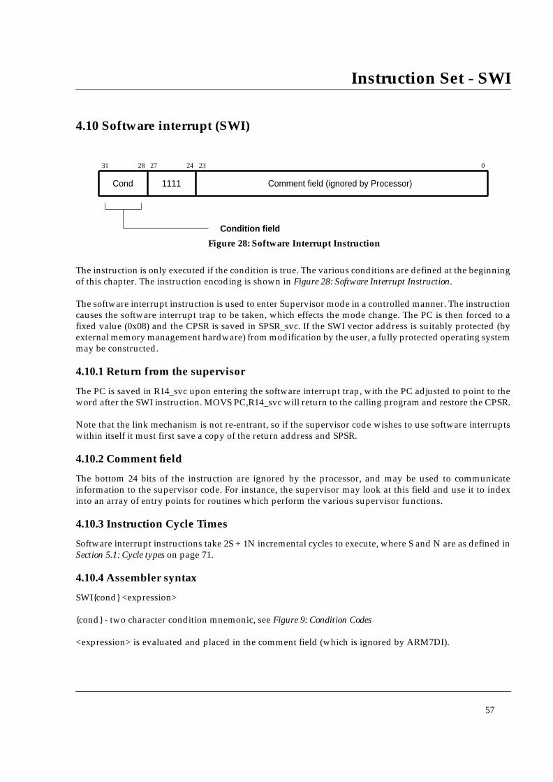
Instruction Set - SWI
57
4.10 Software interrupt (SWI)
Figure 28: Software Interrupt Instruction
The instruction is only executed if the condition is true. The various conditions are defined at the beginningof this chapter. The instruction encoding is shown in Figure 28: Software Interrupt Instruction.
The software interrupt instruction is used to enter Supervisor mode in a controlled manner. The instructioncauses the software interrupt trap to be taken, which effects the mode change. The PC is then forced to afixed value (0x08) and the CPSR is saved in SPSR_svc. If the SWI vector address is suitably protected (byexternal memory management hardware) from modification by the user, a fully protected operating systemmay be constructed.
4.10.1 Return from the supervisor
The PC is saved in R14_svc upon entering the software interrupt trap, with the PC adjusted to point to theword after the SWI instruction. MOVS PC,R14_svc will return to the calling program and restore the CPSR.
Note that the link mechanism is not re-entrant, so if the supervisor code wishes to use software interruptswithin itself it must first save a copy of the return address and SPSR.
4.10.2 Comment field
The bottom 24 bits of the instruction are ignored by the processor, and may be used to communicateinformation to the supervisor code. For instance, the supervisor may look at this field and use it to indexinto an array of entry points for routines which perform the various supervisor functions.
4.10.3 Instruction Cycle Times
Software interrupt instructions take 2S + 1N incremental cycles to execute, where S and N are as defined inSection 5.1: Cycle types on page 71.
4.10.4 Assembler syntax
SWI{cond} <expression>
{cond} - two character condition mnemonic, see Figure 9: Condition Codes
<expression> is evaluated and placed in the comment field (which is ignored by ARM7DI).
31 28 27 24 23 0
Condition field
1111Cond Comment field (ignored by Processor)
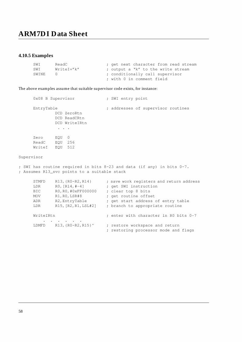
ARM7DI Data Sheet
58
4.10.5 Examples
SWI ReadC ; get next character from read streamSWI WriteI+”k” ; output a “k” to the write streamSWINE 0 ; conditionally call supervisor
; with 0 in comment field
The above examples assume that suitable supervisor code exists, for instance:
0x08 B Supervisor ; SWI entry point
EntryTable ; addresses of supervisor routinesDCD ZeroRtnDCD ReadCRtnDCD WriteIRtn
. . .
Zero EQU 0ReadC EQU 256WriteI EQU 512
Supervisor
; SWI has routine required in bits 8-23 and data (if any) in bits 0-7.; Assumes R13_svc points to a suitable stack
STMFD R13,{R0-R2,R14} ; save work registers and return addressLDR R0,[R14,#-4] ; get SWI instructionBIC R0,R0,#0xFF000000 ; clear top 8 bitsMOV R1,R0,LSR#8 ; get routine offsetADR R2,EntryTable ; get start address of entry tableLDR R15,[R2,R1,LSL#2] ; branch to appropriate routine
WriteIRtn ; enter with character in R0 bits 0-7. . . . . .
LDMFD R13,{R0-R2,R15}^ ; restore workspace and return; restoring processor mode and flags

Instruction Set - CDP
59
4.11 Coprocessor data operations (CDP)
The instruction is only executed if the condition is true. The various conditions are defined at the beginningof this chapter. The instruction encoding is shown in Figure 29: Coprocessor Data Operation Instruction.This class of instruction is used to tell a coprocessor to perform some internal operation. No result iscommunicated back to ARM7DI, and it will not wait for the operation to complete. The coprocessor couldcontain a queue of such instructions awaiting execution, and their execution can overlap other ARM7DIactivity, allowing the coprocessor and to perform independent tasks in parallel.
Figure 29: Coprocessor Data Operation Instruction
4.11.1 The Coprocessor fields
Only bit 4 and bits 24 to 31 are significant toARM7DI . The remaining bits are used by coprocessors. Theabove field names are used by convention, and particular coprocessors may redefine the use of all fieldsexcept CP# as appropriate. The CP# field is used to contain an identifying number (in the range 0 to 15) foreach coprocessor, and a coprocessor will ignore any instruction which does not contain its number in theCP# field.
The conventional interpretation of the instruction is that the coprocessor should perform an operationspecified in the CP Opc field (and possibly in the CP field) on the contents of CRn and CRm, and place theresult in CRd.
4.11.2 Instruction Cycle Times
Coprocessor data operations take 1S + bI incremental cycles to execute, where S and I are as defined inSection 5.1: Cycle types on page 71.
b is the number of cycles spent in the coprocessor busy-wait loop.
Cond
011121516192024272831 23
CRd CP#
78
1110 CP Opc CRn CP 0 CRm
5 4 3
Coprocessor number
Condition field
Coprocessor information Coprocessor operand register
Coprocessor destination register Coprocessor operand register Coprocessor operation code

ARM7DI Data Sheet
60
4.11.3 Assembler syntax
CDP{cond} p#,<expression1>,cd,cn,cm{,<expression2>}
{cond} - two character condition mnemonic, see Figure 9: Condition Codes
p# - the unique number of the required coprocessor
<expression1> - evaluated to a constant and placed in the CP Opc field
cd, cn and cm evaluate to the valid coprocessor register numbers CRd, CRn and CRm respectively
<expression2> - where present is evaluated to a constant and placed in the CP field
4.11.4 Examples
CDP p1,10,c1,c2,c3 ; request coproc 1 to do operation 10; on CR2 and CR3, and put the result in CR1
CDPEQ p2,5,c1,c2,c3,2 ; if Z flag is set request coproc 2 to do; operation 5 (type 2) on CR2 and CR3,; and put the result in CR1

Instruction Set - LDC, STC
61
4.12 Coprocessor data transfers (LDC, STC)
The instruction is only executed if the condition is true. The various conditions are defined at the beginningof this chapter. The instruction encoding is shown in Figure 30: Coprocessor Data Transfer Instructions.This class of instruction is used to load (LDC) or store (STC) a subset of a coprocessors’s registers directlyto memory. ARM7DI is responsible for supplying the memory address, and the coprocessor supplies oraccepts the data and controls the number of words transferred.
Figure 30: Coprocessor Data Transfer Instructions
4.12.1 The Coprocessor fields
The CP# field is used to identify the coprocessor which is required to supply or accept the data, and acoprocessor will only respond if its number matches the contents of this field.
The CRd field and the N bit contain information for the coprocessor which may be interpreted in differentways by different coprocessors, but by convention CRd is the register to be transferred (or the first registerwhere more than one is to be transferred), and the N bit is used to choose one of two transfer length options.For instance N=0 could select the transfer of a single register, and N=1 could select the transfer of all theregisters for context switching.
Cond Rn
0111215161920212425272831
P U W L
2223
110 N CRd CP# Offset
78
Coprocessor number Unsigned 8 bit immediate offset
Base registerLoad/Store bit
0 = Store to memory1 = Load from memory
Write-back bit0 = no write-back1 = write address into base
Coprocessor source/destination register
Pre/Post indexing bit
Up/Down bit0 = down; subtract offset from base1 = up; add offset to base
0 = post; add offset after transfer
Transfer length
Condition field1 = pre; add offset before transfer

ARM7DI Data Sheet
62
4.12.2 Addressing modes
ARM7DI is responsible for providing the address used by the memory system for the transfer, and theaddressing modes available are a subset of those used in single data transfer instructions. Note, however,that the immediate offsets are 8 bits wide and specify word offsets for coprocessor data transfers, whereasthey are 12 bits wide and specify byte offsets for single data transfers.
The 8 bit unsigned immediate offset is shifted left 2 bits and either added to (U=1) or subtracted from (U=0)the base register (Rn); this calculation may be performed either before (P=1) or after (P=0) the base is usedas the transfer address. The modified base value may be overwritten back into the base register (if W=1), orthe old value of the base may be preserved (W=0). Note that post-indexed addressing modes requireexplicit setting of the W bit, unlike LDR and STR which always write-back when post-indexed.
The value of the base register, modified by the offset in a pre-indexed instruction, is used as the address forthe transfer of the first word. The second word (if more than one is transferred) will go to or come from anaddress one word (4 bytes) higher than the first transfer, and the address will be incremented by one wordfor each subsequent transfer.
4.12.3 Address Alignment
The base address should normally be a word aligned quantity. The bottom 2 bits of the address will appearon A[1:0] and might be interpreted by the memory system.
4.12.4 Use of R15
If Rn is R15, the value used will be the address of the instruction plus 8 bytes. Base write-back to R15 shallnot be specified.
4.12.5 Data aborts
If the address is legal but the memory manager generates an abort, the data trap will be taken. The write-back of the modified base will take place, but all other processor state will be preserved. The coprocessor ispartly responsible for ensuring that the data transfer can be restarted after the cause of the abort has beenresolved, and must ensure that any subsequent actions it undertakes can be repeated when the instructionis retried.
4.12.6 Instruction Cycle Times
All LDC instructions are emulated in software: the number of cycles taken will depend on the coprocessorsupport software.
Coprocessor data transfer instructions take (n-1)S + 2N + bI incremental cycles to execute, where S, N andI are as defined in Section 5.1: Cycle types on page 71.
n is the number of words transferred.
b is the number of cycles spent in the coprocessor busy-wait loop.

Instruction Set - LDC, STC
63
4.12.7 Assembler syntax
<LDC|STC>{cond}{L} p#,cd,<Address>
LDC - load from memory to coprocessor
STC - store from coprocessor to memory
{L} - when present perform long transfer (N=1), otherwise perform short transfer (N=0)
{cond} - two character condition mnemonic, see Figure 9: Condition Codes
p# - the unique number of the required coprocessor
cd is an expression evaluating to a valid coprocessor register number that is placed in the CRd field
<Address> can be:
(i) An expression which generates an address:
<expression>
The assembler will attempt to generate an instruction using the PC as a base and a correctedimmediate offset to address the location given by evaluating the expression. This will be a PCrelative, pre-indexed address. If the address is out of range, an error will be generated.
(ii) A pre-indexed addressing specification:
[Rn] offset of zero
[Rn,<#expression>]{!} offset of <expression> bytes
(iii) A post-indexed addressing specification:
[Rn],<#expression> offset of <expression> bytes
Rn is an expression evaluating to a valid ARM7DI register number. Note, if Rn is R15 then the assemblerwill subtract 8 from the offset value to allow for ARM7DI pipelining.
{!} write back the base register (set the W bit) if ! is present
4.12.8 Examples
LDC p1,c2,table ; load c2 of coproc 1 from address table,; using a PC relative address.
STCEQL p2,c3,[R5,#24]! ; conditionally store c3 of coproc 2 into; an address 24 bytes up from R5, write this; address back to R5, and use long transfer; option (probably to store multiple words)
Note that though the address offset is expressed in bytes, the instruction offset field is in words. Theassembler will adjust the offset appropriately.

ARM7DI Data Sheet
64
4.13 Coprocessor register transfers (MRC, MCR)
The instruction is only executed if the condition is true. The various conditions are defined at the beginningof this chapter. The instruction encoding is shown in Figure 31: Coprocessor Register Transfer Instructions.
This class of instruction is used to communicate information directly between ARM7DI and a coprocessor.An example of a coprocessor to ARM7DI register transfer (MRC) instruction would be a FIX of a floatingpoint value held in a coprocessor, where the floating point number is converted into a 32 bit integer withinthe coprocessor, and the result is then transferred to ARM7DI register. A FLOAT of a 32 bit value inARM7DI register into a floating point value within the coprocessor illustrates the use of ARM7DI registerto coprocessor transfer (MCR).
An important use of this instruction is to communicate control information directly from the coprocessorinto the ARM7DI CPSR flags. As an example, the result of a comparison of two floating point values withina coprocessor can be moved to the CPSR to control the subsequent flow of execution.
Figure 31: Coprocessor Register Transfer Instructions
4.13.1 The Coprocessor fields
The CP# field is used, as for all coprocessor instructions, to specify which coprocessor is being called upon.
The CP Opc, CRn, CP and CRm fields are used only by the coprocessor, and the interpretation presentedhere is derived from convention only. Other interpretations are allowed where the coprocessorfunctionality is incompatible with this one. The conventional interpretation is that the CP Opc and CP fieldsspecify the operation the coprocessor is required to perform, CRn is the coprocessor register which is thesource or destination of the transferred information, and CRm is a second coprocessor register which maybe involved in some way which depends on the particular operation specified.
21
Cond
011121516192024272831 23
CP#
78
1110 CRn CP CRm
5 4 3
1LCP Opc Rd
Coprocessor number Coprocessor information Coprocessor operand register
Coprocessor operation mode Condition field
Load/Store bit0 = Store to Co-Processor1 = Load from Co-Processor
ARM source/destination registerCoprocessor source/destination register
Instruction Set - MRC, MCR
65
4.13.2 Transfers to R15
When a coprocessor register transfer to ARM7DI has R15 as the destination, bits 31, 30, 29 and 28 of thetransferred word are copied into the N, Z, C and V flags respectively. The other bits of the transferred wordare ignored, and the PC and other CPSR bits are unaffected by the transfer.
4.13.3 Transfers from R15
A coprocessor register transfer from ARM7DI with R15 as the source register will store the PC+12.
4.13.4 Instruction Cycle Times
MRC instructions take 1S + (b+1)I +1C incremental cycles to execute, where S, I and C are as defined inSection 5.1: Cycle types on page 71.
MCR instructions take 1S + bI +1C incremental cycles to execute.
b is the number of cycles spent in the coprocessor busy-wait loop.
4.13.5 Assembler syntax
<MCR|MRC>{cond} p#,<expression1>,Rd,cn,cm{,<expression2>}
MRC - move from coprocessor to ARM7DI register (L=1)
MCR - move from ARM7DI register to coprocessor (L=0)
{cond} - two character condition mnemonic, see Figure 9: Condition Codes
p# - the unique number of the required coprocessor
<expression1> - evaluated to a constant and placed in the CP Opc field
Rd is an expression evaluating to a valid ARM7DI register number
cn and cm are expressions evaluating to the valid coprocessor register numbers CRn and CRm respectively
<expression2> - where present is evaluated to a constant and placed in the CP field
4.13.6 Examples
MRC 2,5,R3,c5,c6 ; request coproc 2 to perform operation 5; on c5 and c6, and transfer the (single; 32 bit word) result back to R3
MCR 6,0,R4,c6 ; request coproc 6 to perform operation 0; on R4 and place the result in c6
MRCEQ 3,9,R3,c5,c6,2 ; conditionally request coproc 3 to perform; operation 9 (type 2) on c5 and c6, and; transfer the result back to R3

ARM7DI Data Sheet
66
4.14 Undefined instruction
Figure 32: Undefined Instruction
The instruction is only executed if the condition is true. The various conditions are defined at the beginningof this chapter. The instruction format is shown in Figure 32: Undefined Instruction.
If the condition is true, the undefined instruction trap will be taken.
Note that the undefined instruction mechanism involves offering this instruction to any coprocessors whichmay be present, and all coprocessors must refuse to accept it by driving CPA and CPB HIGH.
4.14.1 Instruction cycle times
This cycle takes 2S + 1I + 1N,where S, N and I are as defined in Section 5.1: Cycle types on page 71.
4.14.2 Assembler syntax
At present the assembler has no mnemonics for generating this instruction. If it is adopted in the future forsome specified use, suitable mnemonics will be added to the assembler. Until such time, this instructionshall not be used.
Cond
024272831 5 4 3
1011 xxxx
25
xxxxxxxxxxxxxxxxxxxx

Instruction Set - Examples
67
4.15 Instruction Set Examples
The following examples show ways in which the basic ARM7DI instructions can combine to give efficientcode. None of these methods saves a great deal of execution time (although they may save some), mostlythey just save code.
4.15.1 Using the conditional instructions
(1) using conditionals for logical OR
CMP Rn,#p ; if Rn=p OR Rm=q THEN GOTO LabelBEQ LabelCMP Rm,#qBEQ Label
can be replaced by
CMP Rn,#pCMPNE Rm,#q ; if condition not satisfied try other testBEQ Label
(2) absolute value
TEQ Rn,#0 ; test signRSBMI Rn,Rn,#0 ; and 2's complement if necessary
(3) multiplication by 4, 5 or 6 (run time)
MOV Rc,Ra,LSL#2 ; multiply by 4CMP Rb,#5 ; test valueADDCS Rc,Rc,Ra ; complete multiply by 5ADDHI Rc,Rc,Ra ; complete multiply by 6
(4) combining discrete and range tests
TEQ Rc,#127 ; discrete testCMPNE Rc,#” “-1 ; range testMOVLS Rc,#”.” ; IF Rc<=” “ OR Rc=ASCII(127)
; THEN Rc:=”.”
(5) division and remainder
A number of divide routines for specific applications are provided in source form as part of the ANSI Clibrary provided with the ARM Cross Development Toolkit, available from your supplier. A short generalpurpose divide routine follows.

ARM7DI Data Sheet
68
; enter with numbers in Ra and Rb;
MOV Rcnt,#1 ; bit to control the divisionDiv1 CMP Rb,#0x80000000 ; move Rb until greater than Ra
CMPCC Rb,RaMOVCC Rb,Rb,ASL#1MOVCC Rcnt,Rcnt,ASL#1BCC Div1MOV Rc,#0
Div2 CMP Ra,Rb ; test for possible subtractionSUBCS Ra,Ra,Rb ; subtract if okADDCS Rc,Rc,Rcnt ; put relevant bit into resultMOVS Rcnt,Rcnt,LSR#1 ; shift control bitMOVNE Rb,Rb,LSR#1 ; halve unless finishedBNE Div2
;; divide result in Rc; remainder in Ra
4.15.2 Pseudo random binary sequence generator
It is often necessary to generate (pseudo-) random numbers and the most efficient algorithms are based onshift generators with exclusive-OR feedback rather like a cyclic redundancy check generator. Unfortunatelythe sequence of a 32 bit generator needs more than one feedback tap to be maximal length (i.e. 2^32-1 cyclesbefore repetition), so this example uses a 33 bit register with taps at bits 33 and 20. The basic algorithm isnewbit:=bit 33 eor bit 20, shift left the 33 bit number and put in newbit at the bottom; this operation isperformed for all the newbits needed (i.e. 32 bits). The entire operation can be done in 5 S cycles:
; enter with seed in Ra (32 bits), Rb (1 bit in Rb lsb), uses Rc;
TST Rb,Rb,LSR#1 ; top bit into carryMOVS Rc,Ra,RRX ; 33 bit rotate rightADC Rb,Rb,Rb ; carry into lsb of RbEOR Rc,Rc,Ra,LSL#12 ; (involved!)EOR Ra,Rc,Rc,LSR#20 ; (similarly involved!)
;; new seed in Ra, Rb as before
4.15.3 Multiplication by constant using the barrel shifter
(1) Multiplication by 2^n (1,2,4,8,16,32..)
MOV Ra, Rb, LSL #n
(2) Multiplication by 2^n+1 (3,5,9,17..)
ADD Ra,Ra,Ra,LSL #n

Instruction Set - Examples
69
(3) Multiplication by 2^n-1 (3,7,15..)
RSB Ra,Ra,Ra,LSL #n
(4) Multiplication by 6
ADD Ra,Ra,Ra,LSL #1 ; multiply by 3MOV Ra,Ra,LSL#1 ; and then by 2
(5) Multiply by 10 and add in extra number
ADD Ra,Ra,Ra,LSL#2 ; multiply by 5ADD Ra,Rc,Ra,LSL#1 ; multiply by 2 and add in next digit
(6) General recursive method for Rb := Ra*C, C a constant:
(a) If C even, say C = 2^n*D, D odd:
D=1: MOV Rb,Ra,LSL #nD<>1: {Rb := Ra*D}
MOV Rb,Rb,LSL #n
(b) If C MOD 4 = 1, say C = 2^n*D+1, D odd, n>1:
D=1: ADD Rb,Ra,Ra,LSL #nD<>1: {Rb := Ra*D}
ADD Rb,Ra,Rb,LSL #n
(c) If C MOD 4 = 3, say C = 2^n*D-1, D odd, n>1:
D=1: RSB Rb,Ra,Ra,LSL #nD<>1: {Rb := Ra*D}
RSB Rb,Ra,Rb,LSL #n
This is not quite optimal, but close. An example of its non-optimality is multiply by 45 which is done by:
RSB Rb,Ra,Ra,LSL#2 ; multiply by 3RSB Rb,Ra,Rb,LSL#2 ; multiply by 4*3-1 = 11ADD Rb,Ra,Rb,LSL# 2 ; multiply by 4*11+1 = 45
rather than by:
ADD Rb,Ra,Ra,LSL#3 ; multiply by 9ADD Rb,Rb,Rb,LSL#2 ; multiply by 5*9 = 45

ARM7DI Data Sheet
70
4.15.4 Loading a word from an unknown alignment
; enter with address in Ra (32 bits); uses Rb, Rc; result in Rd.; Note d must be less than c e.g. 0,1;
BIC Rb,Ra,#3 ; get word aligned addressLDMIA Rb,{Rd,Rc} ; get 64 bits containing answerAND Rb,Ra,#3 ; correction factor in bytesMOVS Rb,Rb,LSL#3 ; ...now in bits and test if alignedMOVNE Rd,Rd,LSR Rb ; produce bottom of result word
; (if not aligned)RSBNE Rb,Rb,#32 ; get other shift amountORRNE Rd,Rd,Rc,LSL Rb ; combine two halves to get result
4.15.5 Loading a halfword (Little Endian)
LDR Ra, [Rb,#2] ; Get halfword to bits 15:0MOV Ra,Ra,LSL #16 ; move to topMOV Ra,Ra,LSR #16 ; and back to bottom
; use ASR to get sign extended version
4.15.6 Loading a halfword (Big Endian)
LDR Ra, [Rb,#2] ; Get halfword to bits 31:16MOV Ra,Ra,LSR #16 ; and back to bottom
; use ASR to get sign extended version
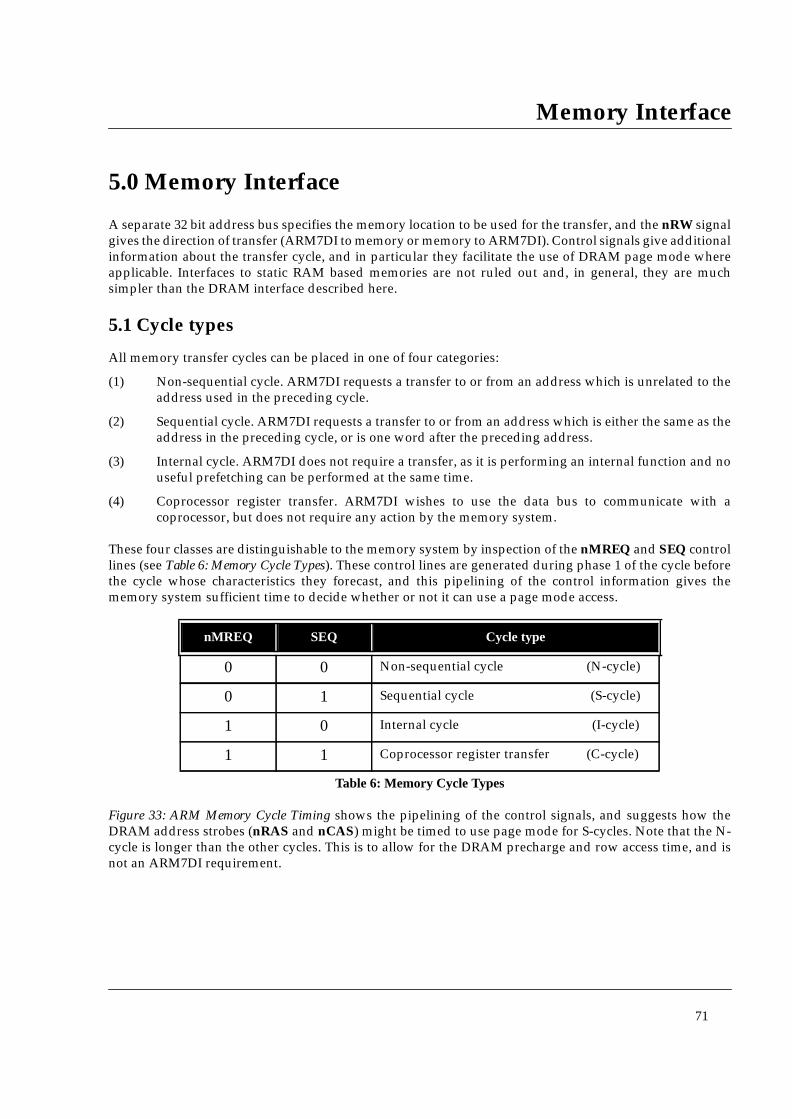
Memory Interface
71
5.0 Memory Interface
A separate 32 bit address bus specifies the memory location to be used for the transfer, and the nRW signalgives the direction of transfer (ARM7DI to memory or memory to ARM7DI). Control signals give additionalinformation about the transfer cycle, and in particular they facilitate the use of DRAM page mode whereapplicable. Interfaces to static RAM based memories are not ruled out and, in general, they are muchsimpler than the DRAM interface described here.
5.1 Cycle types
All memory transfer cycles can be placed in one of four categories:
(1) Non-sequential cycle. ARM7DI requests a transfer to or from an address which is unrelated to theaddress used in the preceding cycle.
(2) Sequential cycle. ARM7DI requests a transfer to or from an address which is either the same as theaddress in the preceding cycle, or is one word after the preceding address.
(3) Internal cycle. ARM7DI does not require a transfer, as it is performing an internal function and nouseful prefetching can be performed at the same time.
(4) Coprocessor register transfer. ARM7DI wishes to use the data bus to communicate with acoprocessor, but does not require any action by the memory system.
These four classes are distinguishable to the memory system by inspection of the nMREQ and SEQ controllines (see Table 6: Memory Cycle Types). These control lines are generated during phase 1 of the cycle beforethe cycle whose characteristics they forecast, and this pipelining of the control information gives thememory system sufficient time to decide whether or not it can use a page mode access.
Figure 33: ARM Memory Cycle Timing shows the pipelining of the control signals, and suggests how theDRAM address strobes (nRAS and nCAS) might be timed to use page mode for S-cycles. Note that the N-cycle is longer than the other cycles. This is to allow for the DRAM precharge and row access time, and isnot an ARM7DI requirement.
nMREQ SEQ Cycle type
0 0 Non-sequential cycle (N-cycle)
0 1 Sequential cycle (S-cycle)
1 0 Internal cycle (I-cycle)
1 1 Coprocessor register transfer (C-cycle)
Table 6: Memory Cycle Types

ARM7DI Data Sheet
72
Figure 33: ARM Memory Cycle Timing
When an S-cycle follows an N-cycle, the address will always be one word greater than the address used inthe N-cycle. This address (marked “a” in the above diagram) should be checked to ensure that it is not thelast in the DRAM page before the memory system commits to the S-cycle. If it is at the page end, the S-cyclecannot be performed in page mode and the memory system will have to perform a full access.
The processor clock must be stretched to match the full access. When an S-cycle follows an I- or C-cycle, theaddress will be the same as that used in the I- or C-cycle. This fact may be used to start the DRAM accessduring the preceding cycle, which enables the S-cycle to run at page mode speed whilst performing a fullDRAM access. This is shown in Figure 34: Memory Cycle Optimization.
5.2 Byte addressing
The processor address bus gives byte addresses, but instructions are always words (where a word is 4bytes) and data quantities are usually words. Single data transfers (LDR and STR) can, however, specifythat a byte quantity is required. The nBW control line is used to request a byte from the memory system;normally it is HIGH, signifying a request for a word quantity, and it goes LOW during phase 2 of thepreceding cycle to request a byte transfer.
When the processor is fetching an instruction from memory, the state of the bottom two address lines A[1:0]is undefined.
When a byte is requested in a read transfer (LDRB), the memory system can safely ignore that the requestis for a byte quantity and present the whole word.
ARM7DI will perform the byte extraction internally. Alternatively, the memory system may activate onlythe addressed byte of the memory. This may be desirable in order to save power, or to enable the use of acommon decoding system for both read and write cycles.
MCLK
A[31:0]
nMREQ
SEQ
nCAS
a a+4
I-cycleS-cycle C-cycleN-cycle
nRAS
D[31:0]
a+8

Memory Interface
73
Figure 34: Memory Cycle Optimization
If a byte write is requested (STRB), ARM7DI will broadcast the byte value across the data bus, presentingit at each byte location within the word. The memory system must decode A[1:0] to enable writing only tothe addressed byte.
One way of implementing the byte decode in a DRAM system is to separate the 32 bit wide block of DRAMinto four byte wide banks, and generate the column address strobes independently as shown in Figure 35:Decoding Byte Accesses to Memory.
When the processor is configured for Little Endian operation byte 0 of the memory system should beconnected to data lines 7 through 0 (D[7:0]) and strobed by nCAS0. nCAS1 drives the bank connected todata lines 15 though 8, and so on. This has the added advantage of reducing the load on each column strobedriver, which improves the precision of this time critical signal.
In the Big Endian case, byte 0 of the memory system should be connected to data lines 31 through 24.
MCLK
A[31:0]
nMREQ
SEQ
nCAS
I-cycle S-cycle
nRAS
D[31:0]

ARM7DI Data Sheet
74
Figure 35: Decoding Byte Accesses to Memory
5.3 Address timing
Normally the processor address changes during phase 2 to the value which the memory system should useduring the following cycle. This gives maximum time for driving the address to large memory arrays, andfor address translation where required. Dynamic memories usually latch the address on chip, and if thelatch is timed correctly they will work even though the address changes before the access has completed.
Static RAMs and ROMs will not work under such circumstances, as they require the address to be stableuntil after the access has completed. Therefore, for use with such devices, the address transition must bedelayed until after the end of phase 2. An on-chip address latch, controlled by ALE, allows the addresstiming to be modified in this way. In a system with a mixture of static and dynamic memories (which forthese purposes means a mixture of devices with and without address latches), the use of ALE may changedynamically from one cycle to the next, at the discretion of the memory system.
5.4 Memory management
The ARM7DI address bus may be processed by an address translation unit before being presented to thememory, and ARM7DI is capable of running a virtual memory system. The abort input to the processormay be used by the memory manager to inform ARM7DI of page faults. Various other signals enabledifferent page protection levels to be supported:
(1) nRW can be used by the memory manager to protect pages from being written to.
(2) nTRANS indicates whether the processor is in user or a privileged mode, and may be used toprotect system pages from the user, or to support completely separate mappings for the system andthe user.
A[0] A[1] nBW MCLK CAS
NCAS0
NCAS1
NCAS2
NCAS3
G
D Q
QuadLatch
Memory Interface
75
Address translation will normally only be necessary on an N-cycle, and this fact may be exploited to reducepower consumption in the memory manager and avoid the translation delay at other times. The times whentranslation is necessary can be deduced by keeping track of the cycle types that the processor uses.
If an N-cycle is matched to a full DRAM access, it will be longer than the minimum processor cycle time.Stretching phase 1 rather than phase 2 will give the translation system more time to generate an abort.
5.5 Locked operations
ARM7DI includes a data swap (SWP) instruction that allows the contents of a memory location to beswapped with the contents of a processor register. This instruction is implemented as an uninterruptablepair of accesses; the first access reads the contents of the memory, and the second writes the register datato the memory. These accesses must be treated as a contiguous operation by the memory controller toprevent another device from changing the affected memory location before the swap is completed.ARM7DI drives the LOCK signal HIGH for the duration of the swap operation to warn the memorycontroller not to give the memory to another device.
5.6 Stretching access times
All memory timing is defined by MCLK, and long access times can be accommodated by stretching thisclock. It is usual to stretch the LOW period of MCLK, as this allows the memory manager to abort theoperation if the access is eventually unsuccessful.
Either MCLK can be stretched before it is applied to ARM7DI, or the nWAIT input can be used togetherwith a free-running MCLK. Taking nWAIT LOW has the same effect as stretching the LOW period ofMCLK, and nWAIT must only change when MCLK is LOW.
ARM7DI does not contain any dynamic logic which relies upon regular clocking to maintain its internalstate. Therefore there is no limit upon the maximum period for which MCLK may be stretched, or nWAITheld LOW.

ARM7DI Data Sheet
76
5.7 The External Data Bus
ARM7DI has a single, bidirectional data bus. Most of the time, the ARM reads from memory and so this busis configured to input. During write cycles however, the ARM7DI must output data. During phase 2 of theprevious cycle, the signal nRW is driven HIGH to indicate a write cycle. During the actual cycle, nENOUTis driven LOW to indicate that the ARM7DI is driving D[31:0] as an output. Figure 36: Data Write Bus Cycleshows this bus timing (DBE has been tied HIGH in this example). Figure 37: ARM7DI Data Bus ControlCircuit shows the circuit which exists in ARM7DI for controlling exactly when the external bus is driven out.
Figure 36: Data Write Bus Cycle
The ARM7DI macrocell has an additional bus control signal, nENIN, which allows the external system tomanually tristate the bus. In the simplest systems, nENIN can be tied LOW and nENOUT can be ignored.However, in many applications when the external data bus is a shared resource, greater control may berequired. In this situation, nENIN can be used to delay when the external bus is driven. Note that forbackwards compatibility, DBEÊis also included. At the macrocell level,DBE and nENIN have almostidentical functionality and in most applications one can be tied off.
Section 5.7.1 Example System: The ARM70D describes how ARM7DI may be interfaced to an external databus, using ARM70D as an example.
ARM7DI has another output control signal called TBE. This signal is normally only used during test andmust be tied HIGH when not in use. When driven LOW, TBE forces all three-stateable outputs to highimpedance. It is as if both DBE and ABE have been driven LOW, causing the data bus, the address bus, andall other signals normally controlled by ABE to become high impedance. Note, however, that there is noscan cell on TBE. Thus, TBE is completely independent of scan data and may be used to put the outputsinto a high impedance state while scan testing takes place.
MCLK
A[31:0]
nRW
nENOUT
D[31:0]
Memory Cycle

Memory Interface
77
Table 7: Output Enable Control Summary shows the tri-state control of ARM7DI’s outputs. Those signalswhich do not have an asterix in the ABE, DBE or TBE column cannot be driven to the high impedance state:
ARM7DI output ABE DBE TBE
A[31:0] * *
D[31:0] * *
nBW * *
nRW * *
LOCK * *
nOPC * *
nTRANS * *
DBGACK
ECLK
nCPI
nENOUT
nEXEC
nM[4:0]
nMREQ
SDOUTMS
SDOUTDATA
SEQ
Table 7: Output Enable Control Summary

ARM7DI Data Sheet
78
Figure 37: ARM7DI Data Bus Control Circuit
5.7.1 Example System: The ARM70D
Connecting ARM7DI's data bus, D[31:0] to an external shared bus requires some simple additional logic.This will vary from application to application. As an example, the following describes how the ARM7Dmacrocell was connected to the bi-directional data bus pads of the ARM70D.
In this application, care must be taken to prevent bus clash on D[31:0] when the data bus drive changesdirection. The timing of nENIN, and the pad control signals must be arranged so that when the core startsto drive out, the pad drive onto D[31:0] switches off before the core starts to drive. Similarly, when the busswitches back to input, the core must stop driving before the pad switches on.
nENOUT
nENIN
D[31:0]
DBE
TBE
Core Control
ScanCell
ScanCell
ScanCell

Memory Interface
79
All this can be achieved using a simple non-overlapping clock generator. The actual circuit implemented inthe ARM70D is shown in Figure 38: The ARM70D Data Bus Circuit. Note that at the core level, TBE and DBEare tied HIGH (inactive). This is because in a packaged part, there is no need to ever manually force theinternal buses into a high impedance state. Note also that at the pad level, the signal EDBE is factored intothe bus control logic. This allows the external memory controller to arbitrate the bus and asynchronouslydisable ARM70D if required.
Figure 38: The ARM70D Data Bus Circuit
Figure 39: Data Bus Control Signal Timing shows how the various control signals interact. Under normalconditions, when the data bus is configured as input, nENOUT is HIGH, nEN1 is LOW, and nEN2/nENINis HIGH. Thus the pads drive XD[31:0] onto D[31:0].
When a write cycle occurs, nRW is driven HIGH to indicate a write during phase 2 of the previous cycle,(ie, with the address). During phase 1 of the actual cycle, nENOUT is driven LOW to indicate that ARM7DIis about to drive the bus. The falling edge of this signal makes nEN1 go HIGH, which disables the input halfpad from driving D[31:0]. This in turn makes nEN2 go LOW, which enables the output half of the pad sothat the ARM70D is now driving the external data bus, XD[31:0]. nEN2 is then buffered and driven backinto the core on nENIN, so that finally the ARM7DI macrocell drives D[31:0]. The delay between all thesignals ensures that there is no clash on the data bus as it changes direction from input to output.
Pad
nENOUT
nENIN
D[31:0]
nEN2
nEN1
XD[31:0]
ARM70D
EDBE
VddDBE
SRL
SRL
SRL
VddTBE
ARM7DCore

ARM7DI Data Sheet
80
Figure 39: Data Bus Control Signal Timing
When the bus turns around to the other direction at the end of the cycle, the various control signals switchthe other way. Again, the non-overlap ensures that there is never a bus clash. This time, nENOUT is drivenHIGH to denote that ARM7DI no longer needs to drive the bus and the core's output is immediatelyswitched off. This causes nEN2 to disable the output half of the pad which in turn causes nEN1 to switchon the input half. Thus, the bus is back to its original input configuration.
Note that the data out time of ARM7DI is not directly determined by nENOUT and nENIN, and sodelaying exactly when the bus is driven will not affect the propagation delay. Please refer to Chapter 11.0AC Parameters for timing details.
nENOUT
nEN1
nEN2 /nENIN
D[31:0]

Coprocessor Interface
81
6.0 Coprocessor Interface
The functionality of the ARM7DI instruction set may be extended by the addition of up to 16 externalcoprocessors. When the coprocessor is not present, instructions intended for it will trap, and suitablesoftware may be installed to emulate its functions. Adding the coprocessor will then increase the systemperformance in a software compatible way. Note that some coprocessor numbers have already beenassigned. Contact ARM Ltd for up to date information.
6.1 Interface signals
Three dedicated signals control the coprocessor interface, nCPI, CPA and CPB. The CPA and CPB inputsshould be driven HIGH except when they are being used for handshaking.
6.1.1 Coprocessor present/absent
ARM7DI takes nCPI LOW whenever it starts to execute a coprocessor (or undefined) instruction. (This willnot happen if the instruction fails to be executed because of the condition codes.) Each coprocessor will havea copy of the instruction, and can inspect the CP# field to see which coprocessor it is for. Every coprocessorin a system must have a unique number and if that number matches the contents of the CP# field thecoprocessor should drive the CPA (coprocessor absent) line LOW. If no coprocessor has a number whichmatches the CP# field, CPA and CPB will remain HIGH, and ARM7DI will take the undefined instructiontrap. Otherwise ARM7DI observes the CPA line going LOW, and waits until the coprocessor is not busy.
6.1.2 Busy-waiting
If CPA goes LOW, ARM7DI will watch the CPB (coprocessor busy) line. Only the coprocessor which isdriving CPA LOW is allowed to drive CPB LOW, and it should do so when it is ready to complete theinstruction. ARM7DI will busy-wait while CPB is HIGH, unless an enabled interrupt occurs, in which caseit will break off from the coprocessor handshake to process the interrupt. Normally ARM7DI will returnfrom processing the interrupt to retry the coprocessor instruction.
When CPB goes LOW, the instruction continues to completion. This will involve data transfers taking placebetween the coprocessor and either ARM7DI or memory, except in the case of coprocessor data operationswhich complete immediately the coprocessor ceases to be busy.
All three interface signals are sampled by both ARM7DI and the coprocessor(s) on the rising edge ofMCLK. If all three are LOW, the instruction is committed to execution, and if transfers are involved theywill start on the next cycle. If nCPI has gone HIGH after being LOW, and before the instruction iscommitted, ARM7DI has broken off from the busy-wait state to service an interrupt. The instruction maybe restarted later, but other coprocessor instructions may come sooner, and the instruction should bediscarded.
ARM7DI Data Sheet
82
6.1.3 Pipeline following
In order to respond correctly when a coprocessor instruction arises, each coprocessor must have a copy ofthe instruction. All ARM7DI instructions are fetched from memory via the main data bus, and coprocessorsare connected to this bus, so they can keep copies of all instructions as they go into the ARM7DI pipeline.The nOPC signal indicates when an instruction fetch is taking place, and MCLK gives the timing of thetransfer, so these may be used together to load an instruction pipeline within the coprocessor.
6.2 Data transfer cycles
Once the coprocessor has gone not-busy in a data transfer instruction, it must supply or accept data at theARM7DI bus rate (defined by MCLK). It can deduce the direction of transfer by inspection of the L bit inthe instruction, but must only drive the bus when permitted to by DBE being HIGH. The coprocessor isresponsible for determining the number of words to be transferred; ARM7DI will continue to increment theaddress by one word per transfer until the coprocessor tells it to stop. The termination condition is indicatedby the coprocessor driving CPA and CPB HIGH.
There is no limit in principle to the number of words which one coprocessor data transfer can move, but byconvention no coprocessor should allow more than 16 words in one instruction. More than this wouldworsen the worst case ARM7DI interrupt latency, as the instruction is not interruptible once the transfershave commenced. At 16 words, this instruction is comparable with a block transfer of 16 registers, andtherefore does not affect the worst case latency.
6.3 Register transfer cycle
The coprocessor register transfer cycle is the one case when ARM7DI requires the data bus withoutrequiring the memory to be active. The memory system is informed that the bus is required by ARM7DItaking both nMREQ and SEQ HIGH. When the bus is free, DBE should be taken HIGH to allow ARM7DIor the coprocessor to drive the bus, and an MCLK cycle times the transfer.
6.4 Privileged instructions
The coprocessor may restrict certain instructions for use in privileged modes only. To do this, thecoprocessor will have to track the nTRANS output.
As an example of the use of this facility, consider the case of a floating point coprocessor (FPU) in a multi-tasking system. The operating system could save all the floating point registers on every task switch, butthis is inefficient in a typical system where only one or two tasks will use floating point operations. Instead,there could be a privileged instruction which turns the FPU on or off. When a task switch happens, theoperating system can turn the FPU off without saving its registers. If the new task attempts an FPUoperation, the FPU will appear to be absent, causing an undefined instruction trap. The operating systemwill then realise that the new task requires the FPU, so it will re-enable it and save FPU registers. The taskcan then use the FPU as normal. If, however, the new task never attempts an FPU operation (as will be thecase for most tasks), the state saving overhead will have been avoided.
Coprocessor Interface
83
6.5 Idempotency
A consequence of the implementation of the coprocessor interface, with the interruptible busy-wait state,is that all instructions may be interrupted at any point up to the time when the coprocessor goes not-busy.If so interrupted, the instruction will normally be restarted from the beginning after the interrupt has beenprocessed. It is therefore essential that any action taken by the coprocessor before it goes not-busy must beidempotent, ie must be repeatable with identical results.
For example, consider a FIX operation in a floating point coprocessor which returns the integer result to anARM7DI register. The coprocessor must stay busy while it performs the floating point to fixed pointconversion, as ARM7DI will expect to receive the integer value on the cycle immediately following thatwhere it goes not-busy. The coprocessor must therefore preserve the original floating point value and notcorrupt it during the conversion, because it will be required again if an interrupt arises during the busyperiod.
The coprocessor data operation class of instruction is not generally subject to idempotency considerations,as the processing activity can take place after the coprocessor goes not-busy. There is no need for ARM7DIto be held up until the result is generated, because the result is confined to stay within the coprocessor.
6.6 Undefined instructions
Undefined instructions are treated by ARM7DI as coprocessor instructions. All coprocessors must beabsent (ie CPA and CPB must be HIGH) when an undefined instruction is presented. ARM7DI will thentake the undefined instruction trap. Note that the coprocessor need only look at bit 27 of the instruction todifferentiate undefined instructions (which all have 0 in bit 27) from coprocessor instructions (which allhave 1 in bit 27).
ARM7DI Data Sheet
84

Debug Interface
85
7.0 Debug Interface
The debug interface is based on the IEEE Std. 1149.1- 1990, “Standard Test Access Port and Boundary-ScanArchitecture” (please refer to this standard for an explanation of the terms used in this section and for adescription of the TAP controller states.)
7.1 Overview
ARM7DI contains hardware support for advanced debugging features. This is intended to ease the user'sdevelopment of application software, operating systems, and the hardware itself.
Simplistically, ARM7DI's debug extensions allow the core to be stopped on a given instruction fetch(breakpoint), or data access (watchpoint), or asynchronously by a debug-request. When this happens,ARM7DI is said to be in debug state. At this point, the core's internal state and the system's external statemay be examined. Once examination is complete, the core and system state may be restored and programexecution may resume.
ARM7DI is forced into debug state either by a request on one of the external debug interface signals, or byan internal functional unit known as ICEBreaker. Once in debug state, the core isolates itself from thememory system. The core can then be examined while all other system activity continues as normal.
ARM7DI's internal state is examined via a JTAG-style serial interface. This allows instructions to be seriallyinserted into the core's pipeline without using the external data bus. Thus, when in debug state, a store-multiple (STM) could be inserted into the instruction pipeline and this would dump the contents ofARM7DI's registers. This data can be serially shifted out without affecting the rest of the system.
7.2 Debug Systems
The ARM7DI forms one component of a debug system that interfaces from the high-level debuggingperformed by the user to the low-level interface supported by ARM7DI. Such a system will typically havethree parts:
1. The Debug Host
This is a computer - for example a PC - running a software debugger such as ARMSD. It allowsthe user to issue high level commands such as “set breakpoint at location XX”, or “examine thecontents of memory from 0x0 to 0x100”.
2. The Protocol Converter
The Debug Host will be connected to the ARM7DI development system via an interface suchas RS232. The messages broadcast over this connection must be converted to the interfacesignals of the ARM7DI, and this function is performed by the protocol converter.
3. ARM7DI
ARM7DI is the lowest level of the system, containing hardware extensions to ease debugging.The debug extensions allow the user to stall the core from program execution, examine itsinternal state and the state of the memory system, and then resume program execution.

ARM7DI Data Sheet
86
These are shown in Figure 40: Typical debug system.
Figure 40: Typical debug system
The anatomy of ARM7DI is shown in Figure 43: ARM7DI Scan Chain Arrangement. The major blocks are:
a) ARM7DM
This is the CPU core, with hardware support for debug.
b) ICEBreaker
This is a set of registers and comparators used to generate debug exceptions (eg breakpoints).This unit is described in full later in this chapter.
c) TAP controller
This controls the action of the scan chains via a JTAG serial interface.
The Debug Host and the Protocol Converter are system dependent. The rest of this chapter is given over tothe hardware debug extensions of ARM7DI.
7.3 Debug Interface Signals
There are three primary external signals associated with the debug interface:
• BREAKPT and DBGRQ with which the system requests ARM7DI to enter debug state.
• DBGACKwhich ARM7DI uses to flag back to the system that it is in debug state.
Host computer running ARMSD
ProtocolConverter
Development SystemContaining ARM7DI
DebugHost
DebugTarget

Debug Interface
87
7.3.1 Entry into Debug State
ARM7DI is forced into debug state after a breakpoint, watchpoint or debug-request has occurred.
Conditions under which a breakpoint or watchpoint occur can be programmed using ICEBreaker.Alternatively, external logic can monitor the address and data bus, and flag breakpoints and watchpointsvia the BREAKPT pin.
The timing is the same for externally generated breakpoints and watchpoints. Data must always be validaround the falling edge of MCLK. If this data is an instruction to be breakpointed, then the BREAKPTsignal must be HIGH around the next rising edge of MCLK. Similarly, if the data is for a load or store, thenthis can be marked as watchpointed by asserting BREAKPT around the next rising edge of MCLK.
When a breakpoint or watchpoint is generated, there may be a delay before ARM7DI enters debug state.When it does, the signal DBGACK is asserted in the HIGH phase of MCLK. The timing for an externallygenerated breakpoint is shown in Figure 41: Debug State Entry.
Entry into debug state on breakpoint
After an instruction has been breakpointed, the core does not enter debug state immediately. Instructionsare marked as being breakpointed as they enter ARM7DI's instruction pipeline. Thus ARM7DI only entersdebug state when (and if) the instruction reaches the pipeline’s execute stage.
A breakpointed instruction may not cause ARM7DI to enter debug state for one of two reasons:
• a branch precedes the breakpointed instruction.When the branch is executed, the instruction pipeline is flushed and the breakpoint iscancelled.
• an exception has occurred.Again, the instruction pipeline is flushed and the breakpoint is cancelled. However, thenormal way to exit from an exception is to branch back to the instruction that would haveexecuted next. This involves refilling the pipeline, and so the breakpoint can be re-flagged.
When a breakpointed conditional instruction reaches the execute stage of the pipeline, the breakpoint isalways taken and ARM7DI enters debug state, regardless of whether the condition was met.

ARM7DI Data Sheet
88
Figure 41: Debug State Entry
Breakpointed instructions do not get executed: instead, ARM7DI enters debug state. Thus, when the internalstate is examined, the state before the breakpointed instruction is seen. Once examination is complete, thebreakpoint should be removed and program execution restarted from the previously breakpointedinstruction.
Entry into debug state on watchpoint
Watchpoints occur on data accesses. A watchpoint is always taken, but the core may not enter debug stateimmediately. In all cases, the current instruction will complete. If this is a multi-word load or store (LDMor STM), then many cycles may elapse before the watchpoint is taken.
Watchpoints can be thought of as being similar to data aborts. The difference is however that if a data abortoccurs, then although the instruction completes, all subsequent changes to ARM7DI’s state are prevented.This allows the cause of the abort to be cured by the abort handler, and the instruction re-executed. This isnot so in the case of a watchpoint. Here, the instruction completes and all changes to the core's state occur(ie load data is written into the destination registers, and base write-back occurs). Thus the instruction doesnot need to be restarted
Watchpoints are always taken. If an exception is pending when a watchpoint occurs, then the core entersdebug state in the mode of that exception.
MCLK
A[31:0]
D[31:0]
BREAKPT
DBGACK
nMREQSEQ
Memory Cycles Internal Cycles

Debug Interface
89
Entry into debug state on debug-request
ARM7DI may also be forced into debug state on debug request. This can be done either through ICEBreakerprogramming (see Chapter 8.0: The ARM7DI ICEBreaker Module on page 109), or by the assertion of theDBGRQ pin. This pin is an asynchronous input and is thus synchronised by logic inside ARM7DI before ittakes effect. Following synchronisation, the core will normally enter debug state at the end of the currentinstruction. However, if the current instruction is a busy-waiting access to a coprocessor, the instructionterminates and ARM7DI enters debug state immediately (this is similar to the action of nIRQ and nFIQ).
Action of ARM7DI in debug state
Once ARM7DI is in debug state, nMREQ and SEQ are forced to indicate internal cycles. This allows the restof the memory system to ignore ARM7DI and functions as normal. Since the rest of the system continuesoperation, ARM7DI must be forced to ignore aborts and interrupts.
When instructions are executed in debug state, ARM7DI outputs (except nMREQ and SEQ) will changeasynchronously to the memory system. For example, every time a new instruction is scanned into thepipeline, the address bus will change. Although this is asynchronous it should not affect the system, sincenMREQ and SEQ are forced to indicate internal cycles regardless of what the rest of ARM7DI is doing. Thememory controller must be designed to ensure that this asynchronous behaviour does not affect the rest ofthe system.
7.4 Scan Chains and JTAG Interface
7.4.1 Overview
There are three JTAG style scan chains inside ARM7DI. These allow testing, debugging and ICEBreakerprogramming. The scan chains are controlled from a JTAG style TAP (Test Access Port) controller. Forfurther details of the JTAG specification, please refer to the IEEE Standard 1149.1 - 1990 “Standard TestAccess Port and Boundary-Scan Architecture”. Note that the scan cells are not fully JTAG compliant. Thefollowing sections describe the limitations on their use.
The three scan paths are referred to as scan chain 0,1 and 2: these are shown in Figure 43: ARM7DI ScanChain Arrangement.
Scan chain 0
Scan chain 0 allows access to the entire periphery of the ARM7DI core, including the data bus. The scanchain functions allow inter-device testing (EXTEST) and serial testing of the core (INTEST).
The order of the scan chain (from SDIN to SDOUTMS) is: data bus bits 0 through 31, the control signals,followed by the address bus bits 31 through 0. See Table 9: Scan Signals and Pins on page 108 for a detailedlisting of the scan order.
Scan chain 1
Scan chain 1 is a subset of the signals that are accessible through scan chain 0. Access to the core's data busD[31:0], and the BREAKPT signal is available serially. There are 33 bits in this scan chain, the order being(from serial data in to out): data bus bits 0 through 31, followed by BREAKPT.

ARM7DI Data Sheet
90
Scan Chain 2
This scan chain simply allows access to the ICEBreaker registers. Refer to Chapter 8.0: The ARM7DIICEBreaker Module on page 109 for details.
7.4.2 The JTAG State Machine
The process of serial test and debug is best explained in conjunction with the JTAG state machine. Figure42: Test Access Port (TAP) Controller State Transitions shows the state transitions that occur in the TAPcontroller.
Figure 42: Test Access Port (TAP) Controller State Transitions
Select-IR-Scan
Capture-IR
tms=0
Shift-IR
tms=0
Exit1-IR
tms=1
Pause-IR
tms=0
Exit2-IR
tms=1
Update-IR
tms=1
tms=0
tms=0
tms=1
tms=1
tms=0
Select-DR-Scan
Capture-DR
tms=0
Shift-DR
tms=0
Exit1-DR
tms=1
Pause-DR
tms=0
Exit2-DR
tms=1
Update-DR
tms=1
Test-Logic Reset
Run-Test/Idle
tms=0tms=1
tms=0
tms=0
tms=0
tms=1
tms=1
tms=0
tms=1 tms=1
tms=1
tms=1 tms=1tms=0 tms=0

Debug Interface
91
7.5 Reset
The boundary-scan interface includes a state-machine controller (the TAP controller). In order to force theTAP controller into the correct state after power-up of the device, a reset pulse must be applied to thenTRST signal. If the boundary scan interface is to be used, then nTRST must be driven LOW, and thenHIGH again. If the boundary scan interface is not to be used, then the nTRST input may be tiedpermanently LOW. Note that a clock on TCK is not necessary to reset the device.
The action of reset is as follows:
System mode is selected (i.e. the boundary scan chain cells do not intercept any of the signalspassing between the external system and the core).
IDcode mode is selected. If the TAP controller is put into the Shift-DR state and TCK is pulsed,the contents of the ID register will be clocked out of TDO.
7.6 Pullup Resistors
The IEEE 1149.1 standard effectively requires that TDI and TMS should have internal pullup resistors. Inorder to minimise static current draw, these resistors are not fitted to ARM7DI. Accordingly, the 4 inputs tothe test interface (the above 3 signals plus TCK) must all be driven to good logic levels to achieve normalcircuit operation.
Figure 43: ARM7DI Scan Chain Arrangement
ARM7DMCore
ARM7DIICEbreaker
ARM7DITAP Controller
•
•
Scan Chain 1
Scan Chain 0
Scan Chain 2

ARM7DI Data Sheet
92
7.7 Instruction Register
The instruction register is 4 bits in length.
There is no parity bit. The fixed value loaded into the instruction register during the CAPTURE-IRcontroller state is: 0001.
7.8 Public Instructions
The following public instructions are supported:
Instruction Binary Code
EXTEST 0000SCAN_N 0010INTEST 1100IDCODE 1110BYPASS 1111CLAMP 0101HIGHZ 0111CLAMPZ 1001SAMPLE/PRELOAD 0011
In the descriptions that follow, TDI and TMS are sampled on the rising edge of TCK and all outputtransitions on TDO occur as a result of the falling edge of TCK.
7.8.1 EXTEST (0000)
The selected scan chain is placed in test mode by the EXTEST instruction.
The EXTEST instruction connects the selected scan chain between TDI and TDO.
When the instruction register is loaded with the EXTEST instruction, all the scan cells are placed in theirtest mode of operation.
In the CAPTURE-DR state, inputs from the system logic and outputs from the output scan cells to thesystem are captured by the scan cells. In the SHIFT-DR state, the previously captured test data is shifted outof the scan chain via TDO, while new test data is shifted in via the TDI input. Note that this data is appliedimmediately to the system logic and system pins.
7.8.2 SCAN_N (0010)
This instruction connects the Scan Path Select Register between TDI and TDO. During the CAPTURE-DRstate, the fixed value 1000 is loaded into the register. During the SHIFT-DR state, the ID number of thedesired scan path is shifted into the scan path select register. In the UPDATE-DR state, the scan register ofthe selected scan chain is connected between TDI and TDO, and remains connected until a subsequentSCAN_N instruction is issued. On reset, scan chain 0 is selected by default. The scan path select register is4 bits long in this implementation, although no finite length is specified.
Debug Interface
93
7.8.3 INTEST (1100)
The selected scan chain is placed in test mode by the INTEST instruction.
The INTEST instruction connects the selected scan chain between TDI and TDO.
When the instruction register is loaded with the INTEST instruction, all the scan cells are placed in their testmode of operation.
In the CAPTURE-DR state, the value of the data applied from the core logic to the output scan cells, and thevalue of the data applied from the system logic to the input scan cells is captured.
In the SHIFT-DR state, the previously captured test data is shifted out of the scan chain via the TDO pin,while new test data is shifted in via the TDI pin.
Single-step operation is possible using the INTEST instruction.
7.8.4 IDCODE (1110)
The IDCODE instruction connects the device identification register (or ID register) between TDI and TDO.The ID register is a 32-bit register that allows the manufacturer, part number and version of a componentto be determined through the TAP.
When the instruction register is loaded with the IDCODE instruction, all the scan cells are placed in theirnormal (system) mode of operation.
In the CAPTURE-DR state, the device identification code (specified at the end of this section) is capturedby the ID register. In the SHIFT-DR state, the previously captured device identification code is shifted outof the ID register via the TDO pin, while data is shifted in via the TDI pin into the ID register. In theUPDATE-DR state, the ID register is unaffected.
7.8.5 BYPASS (1111)
The BYPASS instruction connects a 1 bit shift register (the BYPASS register) between TDI and TDO.
When the BYPASS instruction is loaded into the instruction register, all the scan cells are placed in theirnormal (system) mode of operation. This instruction has no effect on the system pins.
In the CAPTURE-DR state, a logic 0 is captured by the bypass register. In the SHIFT-DR state, test data isshifted into the bypass register via TDI and out via TDO after a delay of one TCK cycle. Note that the firstbit shifted out will be a zero. The bypass register is not affected in the UPDATE-DR state. Note that allunused instruction codes default to the BYPASS instruction.
7.8.6 CLAMP (0101)
This instruction connects a 1 bit shift register (the BYPASS register) between TDI and TDO.

ARM7DI Data Sheet
94
When the CLAMP instruction is loaded into the instruction register, the state of all the output signals isdefined by the values previously loaded into the currently loaded scan chain. Note that this instructionshould only be used when scan chain 0 is the currently selected scan chain.
In the CAPTURE-DR state, a logic 0 is captured by the bypass register. In the SHIFT-DR state, test data isshifted into the bypass register via TDI and out via TDO after a delay of one TCK cycle. Note that the firstbit shifted out will be a zero. The bypass register is not affected in the UPDATE-DR state.
7.8.7 HIGHZ (0111)
This instruction connects a 1 bit shift register (the BYPASS register) between TDI and TDO.
When the HIGHZ instruction is loaded into the instruction register, the Address bus, A[31:0], the data bus,D[31:0], plus nRW, nBW, nOPC, LOCK and nTRANS are all driven to the high impedance state. This is asif the signal TBE had been driven low.
In the CAPTURE-DR state, a logic 0 is captured by the bypass register. In the SHIFT-DR state, test data isshifted into the bypass register via TDI and out via TDO after a delay of one TCK cycle. Note that the firstbit shifted out will be a zero. The bypass register is not affected in the UPDATE-DR state.
7.8.8 CLAMPZ (1001)
This instruction connects a 1 bit shift register (the BYPASS register) between TDI and TDO.
When the CLAMPZ instruction is loaded into the instruction register, all the 3-state outputs (as describedabove) are placed in their inactive state, but the data supplied to the outputs is derived from the scan cells.The purpose of this instruction is to ensure that, during production test, each output can be disabled whenits data value is either a logic 0 or a logic 1.
In the CAPTURE-DR state, a logic 0 is captured by the bypass register. In the SHIFT-DR state, test data isshifted into the bypass register via TDI and out via TDO after a delay of one TCK cycle. Note that the firstbit shifted out will be a zero. The bypass register is not affected in the UPDATE-DR state.
7.8.9 SAMPLE/PRELOAD (0011)
This instruction is included for production test only, and should never be used.
7.9 Test Data Registers
There are 6 test data registers which may be connected between TDI and TDO. They are: Bypass Register,ID Code Register, Scan Chain Select Register, Scan chain 0, 1 or 2. These are now described in detail.

Debug Interface
95
7.9.1 Bypass Register
Purpose: This is a single bit register which can be selected as the path between TDI and TDO to allow thedevice to be bypassed during scan testing.
Length: 1 bit
Operating Mode: When the BYPASS instruction is the current instruction in the instruction register, serialdata is transferred from TDI to TDO in the SHIFT-DR state with a delay of one TCK cycle.
There is no parallel output from the bypass register.
A logic 0 is loaded from the parallel input of the bypass register in the CAPTURE-DR state.
7.9.2 ARM7DI Device Identification (ID) Code Register
Purpose: This register is used to read the 32-bit device identification code. No programmablesupplementary identification code is provided.
Length: 32 bits
The format of the ID register is as follows:
Please contact your supplier for the correct Device Identification Code.
Operating Mode: When the IDCODE instruction is current, the ID register is selected as the serial pathbetween TDI and TDO.
There is no parallel output from the ID register.
The 32-bit device identification code is loaded into the ID register from its parallel inputs during theCAPTURE-DR state.
7.9.3 Instruction Register
Purpose: This is a 4 bit register which is used to change the current TAP instruction.
Length: 4 bits
Operating mode: When in the SHIFT-IR state, the instruction register is selected as the serial path betweenTDI and TDO.
011112272831
1Manufacturer IdentityPart NumberVersion

ARM7DI Data Sheet
96
During the CAPTURE-IR state, the value 0001 binary is loaded into this register. This is shifted out duringSHIFT-IR (lsb first), while a new instruction is shifted in (lsb first). During the UPDATE-IR state, the valuein the instruction register becomes the current instruction. On reset, BYPASS becomes the currentinstruction.
7.9.4 Scan Chain Select Register
Purpose: This is a 4 bit register which is used to change the current active scan chain.
Length: 4 bits
Operating mode: After SCAN_N has been selected as the current instruction, when in the SHIFT-DR state,the Scan Chain Select Register is selected as the serial path between TDI and TDO.
During the CAPTURE-DR state, the value 1000 binary is loaded into this register. This is shifted out duringSHIFT-DR (lsb first), while a new value is shifted in (lsb first). During the UPDATE-DR state, the value inthe register selects a scan chain to become the currently active scan chain. All further instructions such asINTEST then apply to that scan chain.
The currently selected scan chain only changes when a SCAN_N instruction is executed, or a reset occurs.On reset, scan chain 0 is selected as the active scan chain.
7.9.5 Scan Chains 0,1 and 2
These allow serial access to the core logic, and to ICEBreaker for programming purposes. They aredescribed in detail below.
7.9.5.1 Scan Chain 0 and 1
Purpose: To allow access to the ARM7DM CPU core for test and debug.
Length: Scan chain 0: 97 bits, Scan Chain 1: 33 bits.
Each scan chain cell is fairly simple. Each consists of a serial register and a multiplexer. The scan cellsperform two basic functions, capture and shift.
For input cells, the capture stage involves copying the value of the system input to the core into the serialregister. During shift, this value is output serially. The value applied to the core from an input cell is eitherthe system input or the contents of the serial register, and this is controlled by the multiplexer.

Debug Interface
97
Figure 44: Input Scan Cell
For output cells, capture involves placing the value of a core's output into the serial register. During shift,this value is serially output as before. The value applied to the system from an output cell is either the coreoutput, or the contents of the serial register.
All the control signals for the scan cells are generated internally by the TAP controller. The action of theTAP controller is determined by the current instruction, and the state of the TAP state machine. This isdescribed below.
There are three basic modes of operation of the scan chains, INTEST, EXTEST and SYSTEM, and these areselected by the various TAP controller instructions. In SYSTEM mode, the scan cells are idle. System datais applied to inputs, and core outputs are applied to the system. In INTEST mode, the core is internallytested. The data serially scanned in is applied to the core, and the resulting outputs are captured in theoutput cells and scanned out. In EXTEST mode, data is scanned onto the core's outputs and applied to theexternal system. System input data is captured in the input cells and then shifted out.
Note that the scan cells are not fully JTAG compliant in that they do not have an Update stage. Therefore,while data is being moved around the scan chain, the contents of the scan cell is not isolated from theoutput. Thus the output from the scan cell to the core or to the external system could change on every scanclock.
This does not affect ARM7DI since its internal state does not change until it is clocked. The rest of the systemneeds to be aware though that every output could change asynchronously as data is moved around the scanchain. External logic must ensure that this does not harm the rest of the system.
ShiftRegister
Latch
System Data in
SHIFT Clock
Data to Core
Serial Data In
Serial Data Out
CAPTUREClock

ARM7DI Data Sheet
98
Scan chain 0
Scan chain 0 is intended primarily for inter-device testing (EXTEST), and testing the core (INTEST). Scanchain 0 is selected via the SCAN_N TAP Controller instruction.
INTEST allows serial testing of the core. The TAP Controller must be placed in INTEST mode after scanchain 0 has been selected. During CAPTURE-DR, the current outputs from the core's logic are captured inthe output cells. During SHIFT-DR, this captured data is shifted out while a new serial test pattern isscanned in, thus applying known stimuli to the inputs. During RUN-TEST/IDLE, the core is clocked.Normally, the TAP controller should only spend 1 cycle in RUN-TEST/IDLE (see later section for details ofthe core's clocks during test and debug). The whole operation may then be repeated.
EXTEST allows inter-device testing, useful for verifying the connections between devices on a circuit board.The TAP Controller must be placed in EXTEST mode after scan chain 0 has been selected. DuringCAPTURE-DR, the current inputs to the core's logic from the system are captured in the input cells. DuringSHIFT-DR, this captured data is shifted out while a new serial test pattern is scanned in, thus applyingknown values on the core's outputs. During UPDATE-DR, the value shifted into the data bus D[31:0] scancells appears on the outputs. For all other outputs, the value appears as the data is shifted round. Note,during RUN-TEST/IDLE, the core is not clocked. The operation may then be repeated.
Scan chain 1
The primary use for scan chain 1 is for debugging, although it can be used for EXTEST on the data bus. Scanchain 1 is selected via the SCAN_N TAP Controller instruction. Debugging is similar to INTEST, and theprocedure described above for scan chain 0 should be followed.
Note that this scan chain is 33 bits long - 32 bits for the data value, plus the scan cell on the BREAKPT coreinput. This 33rd bit serves 4 purposes. Firstly, under normal INTEST test conditions, this allows a knownvalue to be scanned into the BREAKPT input. Secondly, during EXTEST test conditions, the value appliedto the BREAKPT input from the system can be captured. Thirdly, while debugging, the value placed in the33rd bit determines whether ARM7DI synchronises back to system speed before executing the instruction.SeeSection 7.12.5: System Speed Access for further details. Finally, after ARM7DI has entered debug state, thefirst time this bit is captured and scanned out, its value tells the debugger whether the core entered debugstate due to a breakpoint (bit 33 LOW), or a watchpoint (bit 33 HIGH).
7.9.5.2 Scan Chain 2
Purpose: Scan chain 2 is provided to allow ICEBreaker's registers to be accessed. The order of the scan chain,from TDI to TDO is: read/write, register address bits 4 to 0, followed by data value bits 31 to 0.
Length: 38 bits.
To access this serial register, scan chain 2 must first be selected via the SCAN_N TAP controller instruction.The TAP controller must then be place in INTEST mode. No action is taken during CAPTURE-DR. DuringSHIFT-DR, a data value is shifted into the serial register. Bits 32 to 36 specify the address of the ICEBreakerregister to be accessed. During UPDATE-DR, this register is either read or written depending on the valueof bit 37 (0 = read). Refer to Chapter 8.0: The ARM7DI ICEBreaker Module on page 109 for further details.

Debug Interface
99
7.10 ARM7DI Core Clocks
ARM7DI has two clocks, the memory clock, MCLK, and an internally TCK generated clock, DCLK. Duringnormal operation, the core is clocked by MCLK, and internal logic holds DCLK LOW. When ARM7DI is inthe debug state, the core is clocked by DCLK under control of the TAP state machine, and MCLK may freerun. The selected clock is output on the signal ECLK for use by the external system. Note that when theCPU core is being debugged and is running from DCLK, nWAIT has no effect.
There are two cases in which the clocks switch, during debugging and during testing.
7.10.1 Clock Switch During Debug
When ARM7DI enters debug state, it must switch from MCLK to DCLK. This is handled automatically bylogic in the ARM7DI. On entry to debug state, ARM7DI asserts DBGACK in the HIGH phase of MCLK.The switch between the two clocks occurs on the next falling edge of MCLK. This is shown in Figure 45:Clock Switching on Entry to Debug State.
Figure 45: Clock Switching on Entry to Debug State
ARM7DI is forced to use DCLK as the primary clock until debugging is complete. On exit from debug, thecore must be allowed to synchronise back to MCLK. This must be done in the following sequence. The finalinstruction of the debug sequence must be shifted into the data bus scan chain and clocked in by assertingDCLK. At this point, BYPASS must be clocked into the TAP instruction register. ARM7DI will nowautomatically resynchronise back to MCLK and start fetching instructions from memory at MCLK speed.Please refer also to Section 7.11.3: Exit from Debug State.
7.10.2 Clock Switch During Test
When under serial test conditions - ie when test patterns are being applied to the ARM7DM core throughthe JTAG interface - ARM7DI must be clocked using DCLK. Entry into test is less automatic than debugand some care must be taken.
MCLK
DBGACK
DCLK
ECLK
Multiplexer Switchingpoint

ARM7DI Data Sheet
100
On the way into test, MCLK must be held LOW. The TAP controller can now be used to serially testARM7DI. If scan chain 0 and INTEST are selected, then DCLK is generated while the state machine is in theRUN-TEST/IDLE state. During EXTEST, DCLK is not generated.
On exit from test, BYPASS must be selected as the TAP controller instruction. When this is done, MCLK canbe allowed to resume. After INTEST testing, care should be taken to ensure that the core is in a sensible statebefore switching back. The safest way to do this is to either select BYPASS and then cause a system reset,or to insert MOV PC, #0 into the instruction pipeline before switching back.
7.11 Determining the Core and System State
When ARM7DI is in debug state, the core and system's state may be examined. This is done by forcing loadand store multiples into the instruction pipeline.
7.11.1 Determining the Core’s State
Typically, the first instruction to be executed would be:
STM R0, {R0-R15}
This causes the contents of the registers to be made visible on the data bus. (Note that the use of R0 here isarbitrary, and for illustration only). These values can then be sampled and shifted out.
After determining the values in the current bank of registers, it may be desirable to access the bankedregisters. This can only be done by changing mode. Normally, a mode change may only occur if the core isalready in a privileged mode. However, while in debug state, a mode change from any mode into any othermode may occur. Note that the debugger must restore the original mode before exiting debug state.
For example, assume that the debugger had been asked to return the state of the USER mode and FIQ moderegisters, and debug state was entered in supervisor mode. The instruction sequence could be:
STM R0, {R0-R15} ; Save current registersMRS R0, CPSRSTR R0, R0 ; Save CPSR to determine current modeBIC R0, 0x1F ; Clear mode bitsORR R0, 0x10 ; Select user modeMSR CPSR, R0 ; Enter USER modeSTM R0, {R13,R14} ; Save register not previously visibleORR R0, 0x01 ; Select FIQ modeMSR CPSR, R0 ; Enter FIQ modeSTM R0, {R8-R14} ; Save banked FIQ registers
All these instructions are said to execute at debug speed. Debug speed is much slower than system speedsince between each core clock, 33 scan clocks occur in order to shift in an instruction, or shift out data.Executing instructions more slowly than usual is fine for accessing the core's state since ARM7DI is fullystatic. However, this same method cannot be used for determining the state of the rest of the system.

Debug Interface
101
7.11.2 Determining System State
In order to meet the dynamic timing requirements of the memory system, any attempt to access systemstate must occur synchronously to it. Thus, ARM7DI must be forced to synchronise back to system speed.This is controlled by the 33rd bit of scan chain 1.
Any instruction may be placed in scan chain 1 with bit 33 (the BREAKPT bit) LOW. This instruction willthen be executed at debug speed. To execute an instruction at system speed, the instruction prior to it mustbe scanned into scan chain 1 with bit 33 set HIGH.
After the system speed instruction has been scanned into the data bus and clocked into the pipeline, theBYPASS instruction must be loaded into the TAP controller. This will cause ARM7DI to automaticallysynchronise back to MCLK (the system clock), execute the instruction at system speed, and then re-enterdebug state and switch itself back to the internally generated DCLK. When the instruction has completed,DBGACK will be HIGH and the core will have switched back to DCLK. At this point, INTEST can beselected in the TAP controller, and debugging can resume.
In order to determine that a system speed instruction has completed, the debugger must look at bothDBGACK and nMREQ. In order to access memory, ARM7DI drives nMREQ LOW after it hassynchronised back to system speed. This transition is used by the memory controller to arbitrate whetherARM7DI can have the bus in the next cycle. If the bus is not available, then ARM7DI may have its clockstalled indefinitely. Therefore, the only way to tell that the memory access has completed, is to examine thestate of both nMREQ and DBGACK. When both are HIGH, the access has completed. Usually, thedebugger would be using ICEBreaker to control debugging, and by reading ICEBreaker's status register,the state of nMREQ and DBGACK can be determined. Refer to Chapter 8.0: The ARM7DI ICEBreaker Moduleon page 109 for more details.
By the use of system speed load multiples and debug speed store multiples, the state of the system'smemory can be fed back to the debug host.
There are restrictions on which instructions may have the 33rd bit set. The only valid instructions on whichto set this bit are loads, stores, load multiple and store multiple. See also Section 7.11.3: Exit from Debug State.When ARM7DI returns to debug state after a system speed access, bit 33 of scan chain 1 is set HIGH. Thisgives the debugger information about why the core entered debug state the first time this scan chain is read.
7.11.3 Exit from Debug State
Leaving debug state involves restoring ARM7DI's internal state, causing a branch to the next instruction tobe executed, and synchronising back to MCLK. After restoring internal state, a branch instruction must beloaded into the pipeline. See Section 7.12: The PC's Behaviour During Debug for details on calculating thebranch.
Bit 33 of scan chain 1 is used to force ARM7DI to resynchronise back to MCLK. The penultimate instructionof the debug sequence is scanned in with bit 33 set HIGH. The final instruction of the debug sequence is thebranch, and this is scanned in with bit 33 LOW. The core is then clocked to load the branch into the pipeline.Now, the BYPASS instruction is selected in the TAP controller. This allows the scan chain to go back tosystem mode and allows resynchronisation to occur. ARM7DI then resumes normal operation, fetchinginstructions from memory.

ARM7DI Data Sheet
102
The function of DBGACK is to tell the rest of the system when ARM7DI is in debug state. This can be usedto inhibit peripherals such as watchdog timers which have real time characteristics. Also, DBGACK can beused to mask out memory accesses which are caused by the debugging process. For example, whenARM7DI enters debug state after a breakpoint, the instruction pipeline contains the breakpointedinstruction plus two other instructions which have been prefetched. On entry to debug state, the pipelineis flushed. Therefore, on exit from debug state, the pipeline must be refilled to its previous state. Thus,because of the debugging process, more memory accesses occur than would normally be expected. Anysystem peripheral which may be sensitive to the number of memory accesses can be inhibited through theuse of DBGACK.
For example, imagine a fictitious peripheral that simply counts the number of memory cycles. This deviceshould return the same answer after a program has been run both with and without debugging. Figure 46:Debug Exit Sequence shows the behaviour of ARM7DI on exit from the debug state.
Figure 46: Debug Exit Sequence
It can be seen from Figure 41: Debug State Entry that the final memory access occurs in the cycle afterDBGACK goes HIGH, and this is the point at which the cycle counter should be disabled. Figure 46: DebugExit Sequence shows that the first memory access that the cycle counter has not seen before occurs in thecycle after DBGACK goes LOW, and so this is the point at which the counter should be re-enabled.
Note that when a system speed access from debug state occurs, ARM7DI temporarily drops out of debugstate, and so DBGACK can go LOW. If there are peripherals which are sensitive to the number of memoryaccesses, then they must be led to believe that ARM7DI is still in debug state. By programming theICEBreaker control register, the value on DBGACK can be forced to be HIGH. See Chapter 8.0: The ARM7DIICEBreaker Module on page 109 for more details.
ECLK
nMREQSEQ
A[31:0]
D[31:0]
DBGACK
Internal Cycles N S S
Ab Ab+4 Ab+8

Debug Interface
103
7.12 The PC's Behaviour During Debug
In order that ARM7DI may be forced to branch back to the place at which program flow was interruptedby debug, the debugger must keep track of what happens to the PC. There are five cases: breakpoint,watchpoint, watchpoint when another exception occurs, debug request and system speed access.
7.12.1 Breakpoint
Entry to the debug state from a breakpoint advances the PC by 4 addresses, or 16 bytes. Each instructionexecuted in debug state advances the PC by 1 address, or 4 bytes. The normal way to exit from debug stateafter a breakpoint is to remove the breakpoint, and branch back to the previously breakpointed address.
For example, if ARM7DI entered debug state from a breakpoint set on a given address and 2 debug speedinstructions were executed, then a branch of -7 addresses must occur (4 for debug entry, +2 for theinstructions, +1 for the final branch). The following sequence shows the data scanned into scan chain 1. Thisis msb first, and so the first digit is the value placed in the BREAKPT bit, followed by the instruction data.
0 E0802000 ; ADD R2, R0, R01 E1826001 ; ORR R6, R2, R10 EAFFFFF9 ; B -7 (2's complement)
Note that once in debug state, a minimum of two instructions must be executed before the branch, althoughthese may both be NOPs (MOV R0, R0). For small branches, the final branch could be replaced with asubtract with the PC as the destination (SUB PC, PC, #28 in the above example).
7.12.2 Watchpoints
Returning to program execution after entering debug state from a watchpoint is done in the same way asthe procedure described above. Debug entry adds 4 addresses to the PC, and every instruction adds 1address. The difference is that since the instruction that caused the watchpoint has executed, the programreturns to the next instruction.
7.12.3 Watchpoint with another Exception
If a watchpointed access simultaneously causes a data abort, then ARM7DI will enter debug state in abortmode. Entry into debug is held off until the core has changed into abort mode, and fetched the instructionfrom the abort vector.
A similar sequence is followed when an interrupt - or any other exception - occurs during a watchpointedmemory access. ARM7DI will enter debug state in the exception's mode, and so the debugger must checkto see whether this happened. The debugger can deduce whether an exception occurred by looking at thecurrent and previous mode (in the CPSR and SPSR), and the value of the PC. If an exception did take place,then the user should be given the choice of whether to service the exception before debugging.
Exiting debug state if an exception occurred is slightly different from the other cases. Here, entry to debugstate causes the PC to be incremented by 3 addresses rather than 4, and this must be taken into account inthe return branch calculation. For example, suppose that an abort occurred on a watchpointed access and10 instructions had been executed to determine this. The following sequence could be used to return toprogram execution.

ARM7DI Data Sheet
104
0 E1A00000 ; MOV R0, R01 E1A00000 ; MOV R0, R00 EAFFFFF0 ; B -16
This will force a branch back to the abort vector, causing the instruction at that location to be refetched andexecuted. Note that after the abort service routine, the instruction which caused the abort and watchpointwill be reexecuted. This will cause the watchpoint to be generated and hence ARM7DI will enter debugstate again.
7.12.4 Debug Request
Entry into debug state via a debug request is similar to a breakpoint. However, unlike a breakpoint, the lastinstruction will have completed execution and so must not be refetched on exit from debug state. Therefore,it can be thought that entry to debug state adds 3 addresses to the PC, and every instruction executed indebug state adds 1.
For example, suppose that the user has invoked a debug request, and decides to return to programexecution straight away. The following sequence could be used:
0 E1A00000 ; MOV R0, R01 E1A00000 ; MOV R0, R00 EAFFFFFA ; B -6
This restores the PC, and restarts the program from the next instruction.
7.12.5 System Speed Access
If a system speed access is performed during debug state, the value of the PC is increased by 3 addresses.Since system speed instructions access the memory system, it is possible for aborts to take place. If an abortoccurs during a system speed memory access, ARM7DI enters abort mode before returning to debug state.
This is similar to an aborted watchpoint except that the problem is much harder to fix, because the abortwas not caused by an instruction in the main program, and the PC does not point to the instruction whichcaused the abort. An abort handler usually looks at the PC to determine the instruction which caused theabort, and hence the abort address. In this case, the value of the PC is invalid, but the debugger should knowwhat location was being accessed. Thus the debugger can be written to help the abort handler fix thememory system.
7.12.6 Summary of Return Address Calculations
The calculation of the branch return address can be summarised as follows:
a) For normal breakpoint and watchpoint, the branch is:
- (4 + N + 3S)
b) For entry through debug request (DBGRQ), or watchpoint with exception, the branch is:

Debug Interface
105
- (3 + N + 3S)
where N is the number of debug speed instructions executed (including the final branch), and S is thenumber of system speed instructions executed.
7.13 Priorities / Exceptions
Because the normal program flow is broken when a breakpoint or a debug request occurs, debug can bethought of as being another type of exception. Some of the interaction with other exceptions has beendescribed above. This section summarises the priorities.
7.13.1 Breakpoint with Prefetch Abort
When a breakpointed instruction fetch causes a prefetch abort, the abort is taken and the breakpoint isdisregarded. Normally, prefetch aborts occur when, for example, an access is made to a virtual addresswhich does not physically exist, and the returned data is therefore invalid. In such a case the operatingsystem’s normal action will be to swap in the page of memory and return to the previously invalid address.This time, when the instruction is fetched, and providing the breakpoint is activated (it may be datadependent), ARM7DI will enter debug state.
Thus the prefetch abort takes higher priority than the breakpoint.
7.13.2 Interrupts
When ARM7DI enters debug state, interrupts are automatically disabled. If interrupts are disabled duringdebug, ARM7DI will never be forced into an interrupt mode.
If an interrupt was pending during the instruction prior to entering debug state, then ARM7DI will enterdebug state in the mode of the interrupt. Thus, on entry to debug state, the debugger cannot assume thatARM7DI will be in the expected mode of the user's program. It must check the PC, the CPSR and the SPSRto fully determine the reason for the exception.
Thus, debug takes higher priority than the interrupt, although ARM7DI remembers that an interrupt hasoccurred.
7.13.3 Data Aborts
As described above, when a data abort occurs on a watchpointed access, ARM7DI enters debug state inabort mode. Thus the watchpoint has higher priority than the abort, although, as in the case of interrupt,ARM7DI remembers that the abort happened.

ARM7DI Data Sheet
106
7.14 Scan Interface Signals
Figure 47: Scan General Timing
Figure 48: Scan 3-state Timing
Symbol Parameter Min Typ Max Units Notes
Tbscl TCK low period TBD ns
Tbsch TCK high period TBD ns
Tbsis TDI ,TMS setup to [TCr] TBD ns
Tbsih TDI ,TMS hold from [TCr] TBD ns
Table 8: ARM7DI Scan Interface Timing
TCK
TMSTDI
TDO
Data In
Data Out
Tbscl Tbsch
Tbsis Tbsih
TbsohTbsod
Tbsss Tbssh
TbsdhTbsdd
TCK
TDO
Data Out
Tbsoe Tbsoz
Tbsde Tbsdz

Debug Interface
107
Please note that the above figures are provisional.
Notes:
1. Assumes a 25pF load on TDO. Output timing derates at 0.072ns/pF of extra load applied.
2. TDO enable time applies when the TAP controller enters the Shift-DR or Shift-IR states.
3. TDO disable time applies when the TAP controller leaves the Shift-DR or Shift-IR states.
4. For correct data latching, the I/O signals (from the core and the pads) must be setup and heldwith respect to the rising edge of TCK in the CAPTURE-DR state of the INTEST and EXTESTinstructions.
5. Assumes that the data outputs are loaded with the AC test loads (see AC parameterspecification).
6. Data output enable time applies when the scan logic is used to enable the output drivers.
7. Data output disable time applies when the scan logic is used to disable the output drivers.
Tbsoh TDO hold time 5 ns 1
Tbsod TCf toTDO valid 40 ns 1
Tbsss I/O signal setup to [TCr] 5 ns 4
Tbssh I/O signal hold from [TCr] 20 ns 4
Tbsdh data output hold time 5 ns 5
Tbsdd TCf to data output valid 40 ns
Tbsoe TDO enable time 5 ns 1,2
Tbsoz TDO disable time 40 ns 1,3
Tbsde data output enable time 5 ns 5,6
Tbsdz data output disable time 40 ns 5,7
Symbol Parameter Min Typ Max Units Notes
Table 8: ARM7DI Scan Interface Timing

ARM7DI Data Sheet
108
Key: I - Input
O - Output
I/O - Input / Output
No Signal Type No Signal Type No Signal Type No Signal Type
1 D[0] I/O 26 D[25] I/O 51 nOPC O 76 A[21] O2 D[1] I/O 27 D[26] I/O 52 IFEN I 77 A[20] O3 D[2] I/O 28 D[27] I/O 53 nCPI O 78 A[19] O4 D[3] I/O 29 D[28] I/O 54 nMREQ O 79 A[18] O5 D[4] I/O 30 D[29] I/O 55 SEQ O 80 A[17] O6 D[5] I/O 31 D[30] I/O 56 nTRANS O 81 A[16] O7 D[6] I/O 32 D[31] I/O 57 CPB I 82 A[15] O8 D[7] I/O 33 BREAKPT I 58 nM[4] O 83 A[14] O9 D[8] I/O 34 NENIN I 59 nM[3] O 84 A[13] O10 D[9] I/O 35 NENOUT O 60 nM[2] O 85 A[12] O11 D[10] I/O 36 LOCK O 61 nM[1] O 86 A[11] O12 D[11] I/O 37 BIGEND I 62 nM[0] O 87 A[10] O13 D[12] I/O 38 DBE I 63 nEXEC O 88 A[9] O14 D[13] I/O 39 nBW O 64 ALE I 89 A[8] O15 D[14] I/O 40 DBGACK O 65 ABE I 90 A[7] O16 D[15] I/O 41 nFIQ I 66 A[31] O 91 A[6] O17 D[16] I/O 42 nIRQ I 67 A[30] O 92 A[5] O18 D[17] I/O 43 nRESET I 68 A[29] O 93 A[4] O19 D[18] I/O 44 DATA32 I 69 A[28] O 94 A[3] O20 D[19] I/O 45 ISYNC I 70 A[27] O 95 A[2] O21 D[20] I/O 46 DBGRQ I 71 A[26] O 96 A[1] O22 D[21] I/O 47 nRW O 72 A[25] O 97 A[0] O23 D[22] I/O 48 ABORT I 73 A[24] O24 D[23] I/O 49 CPA I 74 A[23] O25 D[24] I/O 50 PROG32 I 75 A[22] O
Table 9: Scan Signals and Pins

The ARM7DI ICEBreaker Module
109
8.0 The ARM7DI ICEBreaker Module
The ARM7DI-ICEbreaker module - hereafter referred to simply as ICEbreaker - provides integrated on-chipdebug support for the ARM7D CPU core. ICEbreaker consists of two real time watchpoint registers,together with a control and status register. One or both of the watchpoint registers can be programmed tohalt execution of instructions by the ARM7D CPU core via its BREAKPT signal. Execution is halted whena match occurs between the values programmed into ICEbreaker and the values currently appearing on theaddress bus, data bus and various control signals. Any bit can be masked so that its value does not affectthe comparison.
Figure 49: ARM7DI Block Diagram shows the relationship between ARM7D, ICEbreaker and the TAPcontroller. Only those ARM7DI signals that are pertinent to ICEbreaker are shown.
Figure 49: ARM7DI Block Diagram
A[31:0]
D[31:0]
NOPC
NRW
NBW
NTRANS
DBGACK
BREAKPT
DBGRQ
IFEN
ECLK
NMREQ
EXTERN1
EXTERN0
BREAKPT
DBGRQ
DBGACK
TCK
DBGEN
TAP
ICEBreakerARM7DM
TMS
TDITDO
SDIN SDOUT
ARM7DMI
int
int
int
nTRST

ARM7DI Data Sheet
110
Either watchpoint register can be configured as a watchpoint (data access) or a breakpoint (instructionfetch) by suitable programming of the value and mask registers. A particular feature of ICEbreaker is thatboth watchpoints and breakpoints can be data-dependent.
Independent Debug Control and Debug Status registers are used to provide overall control of ICEbreaker'soperation. ICEbreaker is programmed in a serial fashion using the ARM7DI TAP controller.
8.1 The Watchpoint Registers
ICEbreaker consists of two watchpoint registers, known as Watchpoint 0 and Watchpoint 1. Each watchpointregister consists of 6 independently programmable registers. These are:
• 32-bit Address Value register
• 32-bit Address Mask register
• 32-bit Data Value register
• 32-bit Data Mask register
• 8-bit Control Value register
• 7-bit Control Mask register
In addition, there are two global registers which provide overall control and status:
• 3-bit Debug Control register
• 4-bit Debug Status register
Each register is programmed by scanning appropriate data into the ICEbreaker scan chain (scan chain 2).The scan chain register consists of a 38-bit shift register comprising a 32-bit data field, a 5-bit address fieldand a read/write bit - see Figure 50: ICEBreaker Block Diagram.
Programming a register is achieved by scanning the data to be written into the 32-bit data field, the addressof the register into the 5-bit address field and a '1' into the read/write bit.
Reading a register is achieved by scanning the address of the register into the 5-bit address field and a '0'into the read/write bit. The 32-bit data field is ignored in the case of reads.
Reading or writing of the register actually occurs when the TAP controller enters the UPDATE-DR state(see Section 7.4: Scan Chains and JTAG Interface on page 89).

The ARM7DI ICEBreaker Module
111
Figure 50: ICEBreaker Block Diagram
Addr
Data
AddressDecoder
Update
32
r/w
TDI TDO
A[31:0]D[31:0]
+
Registers/comparators
BREAKPOINT
0
31
0
4
Control

ARM7DI Data Sheet
112
The registers are mapped as shown in Table 10: Function and Mapping of ICEBreaker Registers.
The location of bits in the Control Value and Mask registers is shown in Figure 51: ICEBreaker WatchpointControl Value and Mask Registers.
The control value and mask registers are mapped identically in the lower 7 bits. Bit 7 of the control valueregister is the ENABLE bit, which cannot be masked.
Figure 51: ICEBreaker Watchpoint Control Value and Mask Registers
Address Width Function
00000 3 Debug Control Register
00001 4 Debug Status Register
01000 32 Watchpoint 0 Address Value Register
01001 32 Watchpoint 0 Address Mask Register
01010 32 Watchpoint 0 Data Value Register
01011 32 Watchpoint 0 Data Mask Register
01100 8 Watchpoint 0 Control Value Register
01101 7 Watchpoint 0 Control Mask Register
10000 32 Watchpoint 1 Address Value Register
10001 32 Watchpoint 1 Address Mask Register
10010 32 Watchpoint 1 Data Value Register
10011 32 Watchpoint 1 Data Mask Register
10100 8 Watchpoint 1 Control Value Register
10101 7 Watchpoint 1 Control Mask Register
Table 10: Function and Mapping of ICEBreaker Registers
7 6 5 4 3 2 1 0
ENABLE RANGE CHAIN EXTERN nTRANS nOPC nBW nRW
The ARM7DI ICEBreaker Module
113
nRW : This compares against the not read/write signal from the ARM7D core in order to detect thedirection of bus activity. nRW=0 for a read cycle and nRW=1 for a write cycle.
nBW : This compares against the not byte/word signal from the ARM7D core in order to detect thesize of bus activity. nBW=0 for a byte access and nBW=1 for a word access.
nOPC : This is used to detect whether the current cycle is an instruction fetch (nOPC=0) or a dataaccess (nOPC=1).
nTRANS : This compares against the not translate signal from the ARM7DI core in order to distinguishbetween User mode (nTRANS=0) and non-User mode (nTRANS=1) accesses.
EXTERN : This is an external input to ICEbreaker which allows the watchpoint to be dependent uponsome external condition. The EXTERN input for Watchpoint 0 is labelled EXTERN0 and theEXTERN input for Watchpoint 1 is labelled EXTERN1.
CHAIN : This can be connected to the chain output of another watchpoint register in order toimplement, for example, debugger requests of the form 'breakpoint on address YYY only whenin process XXX'. In the ARM7DI-ICEbreaker, the CHAINOUT output of watchpoint register 1is connected to the CHAIN input of watchpoint register 0. The CHAINOUT output is derivedfrom a latch; the address/control field comparator drives the write enable for the latch and theinput to the latch is the value of the data field comparator. The CHAINOUT latch is clearedwhen the Control Value register is written or when NTRST is LOW.
RANGE : This can be connected to the range output of another watchpoint register. In the ARM7DI-ICEbreaker, the RANGEOUT output of watchpoint register 1 is connected to the RANGEinput of watchpoint register 0. This allows the two watchpoints to be coupled for detectingconditions that occur simultaneously, eg. for range-checking.
ENABLE : If a watchpoint match occurs, the BREAKPT signal will only be asserted when the ENABLEbit is set. This bit only exists in the value register: it cannot be masked.
For each of the bits 6:0 in the value register, there is a corresponding bit in the mask register. This allowsthe dependency on particular signals to be removed. For example, if a watchpoint is required on aparticular memory location, but the data value is irrelevant, then the mask register can be programmed tomake the entire data bus field 'don't care'. Note that the mask is an XNOR mask rather than a conventionalAND mask: by setting the mask bit to a '1', the comparator for that bit position will always match,irrespective of the value register or the input value.
Setting the mask bit to '0' means that the comparator will only match if the input value matches the valueprogrammed into the value register.
8.1.1 Programming the Watchpoint Registers
An ICEbreaker watchpoint register can be configured as a breakpoint (for instruction fetches) or as awatchpoint (for data accesses). Breakpoints can be further classified as hardware breakpoints or softwarebreakpoints. Hardware breakpoints typically monitor the address value and can be set in any code, even incode that is in ROM and self-modifying code. Conversely, software breakpoints monitor a particular bit

ARM7DI Data Sheet
114
pattern being fetched from any address; one ICEbreaker watchpoint register can thus be used to supportany number of software breakpoints. Software breakpoints can normally only be set in RAM because aninstruction has to be replaced by the special bit pattern chosen to cause a software breakpoint.
8.1.2 Programming Hardware Breakpoints
The watchpoint register can be used to cause hardware breakpoints (i.e. on instruction fetches) byprogramming it in the following way:
• Program the address value register with the address of the instruction to be breakpointed
• Program the address mask register with '11' in bits [1:0] (since A[1:0] are don't care values oninstruction fetches) and with ’0’ in all other bits.
• Program the data value register only if a data-dependent breakpoint is required; i.e. only if theactual instruction code fetched must be matched as well as the address.
• If the data value is a don't care, program the data mask register to all '1's, otherwise program it toall '0's.
• Program the control value register with nOPC=0, all other bits are don't care
• Program the control mask register with nOPC=0, all other bits to '1'
• If the distinction between user and non-user mode instruction fetches is to be made, then thenTRANS value and mask register bits must also be programmed accordingly.
• The EXTERN, RANGE and CHAIN bits may also be programmed if desired.
8.1.3 Programming Software Breakpoints
The watchpoint register can be used to cause software breakpoints (i.e. on instruction fetches of a particularbit pattern) by programming it in the following way:
• The address value register need not be programmed.
• Program the address mask register with all '1's so that the address is a don't care.
• Program the data value register with the particular bit pattern that has been chosen to represent asoftware breakpoint.
• Program the data mask register to all '0's
• Program the control value register with nOPC=0, all other bits are don't care
• Program the control mask register with nOPC=0, all other bits to '1'
• If the distinction between user and non-user mode instruction fetches is to be made, then thenTRANS value and mask register bits must also be programmed accordingly.
• The EXTERN, RANGE and CHAIN bits may also be programmed if desired.

The ARM7DI ICEBreaker Module
115
Then to set a software breakpoint, the instruction at the desired address should be read and stored away.Then the special bit pattern that represents a software breakpoint should be written at that address. Thisprocess may be repeated as many times as necessary. To clear a software breakpoint, the previously storedaway instruction should be restored.
8.1.4 Programming Watchpoints
The watchpoint register can be used to cause watchpoints (i.e. on data accesses) by programming it in thefollowing way:
• Program the address value register with the address of the data access to be watchpointed.
• Program the address mask register with all 0's
• Program the data value register only if a data-dependent watchpoint is required; i.e. only if theactual data value that is read or written must be matched as well as the address.
• If the data value is a don't care, program the data mask register to all '1's, otherwise program it toall '0's.
• Program the control value register with nOPC=1, nRW=0 for a read or nRW=1 for a write, nBW=0for a byte access or nBW=1 for a word access
• Program the control mask register with nOPC=0, nRW=0, nBW=0, all other bits to '1'. Note thatnRW or nBW may be set to '1' if both reads and writes or both byte and word accesses respectivelyare to be watchpointed.
• If the distinction between user and non-user mode data accesses is to be made, then the nTRANSvalue and mask register bits must also be programmed accordingly.
• The EXTERN, RANGE and CHAIN bits may also be programmed if desired.
Note that the above are just examples of how to program the watchpoint register to generate breakpointsand watchpoints; many other ways of programming the registers are possible. For instance, by setting oneor more of the address mask bits, simple range breakpoints can be provided.
8.2 The Debug Control Register
The Debug Control Register is 3 bits wide. If the register is accessed for a write (with the read/write bitHIGH), then the control bits are written. If the register is accessed for a read (with the read/write bit LOW),then the control bits are read. The function and mapping of the Debug Control Register is shown below:
Address Width Function
00000 3 Debug Control
Table 11: Debug Control Register - Function and Mapping

ARM7DI Data Sheet
116
The function of each bit in this register is as follows:
Bit 2: INTDISBit 1: DBGRQBit 0: DBGACK
Bits 1 and 0 allow the values on DBGRQ and DBGACK to be forced. In the case of DBGRQ, the value heldin bit 1 of the Debug Control register is logically OR'ed with the external DBGRQ before being applied tothe core. In the case of DBGACK, the value of DBGACK from the ARM7D core is OR'ed with the valueheld in bit 0 to generate the external value of DBGACK seen at the periphery of ARM7DI. This allows thedebug system to signal to the rest of the system that the ARM7D is still being debugged even when system-speed accesses are being performed (in which case the internal DBGACK signal from the ARM7D core willbe LOW).
If Bit 2 (INTDIS) is asserted, then the interrupt enable signal (IFEN) of the ARM7D core is forced LOW.Thus all interrupts (IRQ and FIQ) are disabled during debugging (DBGACK=1) or if the INTDIS bit isasserted. The IFEN signal is driven according to the following table:
8.3 Debug Status Register
The Debug Status Register is 4 bits wide. If the register is accessed for a write (with the read/write bit high),then the status bits are written. If the register is accessed for a read (with the read/write bit LOW), then thestatus bits are read. The function and mapping of the Debug Status Register is shown below:
DBGACK (from core) INTDIS IFEN
0 0 1
1 x 0
x 1 0
Table 12: IFEN signal control
Address Width Function
00001 4 Debug Status
Table 13: Debug Status Register - Function and Mapping

The ARM7DI ICEBreaker Module
117
The function of each bit in this register is as follows:
Bit 3 : nMREQBit 2 : IFENBit 1 : DBGRQBit 0 : DBGACK
Bits 1 and 0 allow the values on the synchronised versions of DBGRQ and DBGACK to be read.
Bit 2 allows the state of the interrupt enable pin (IFEN) of the ARM7D core to be read. Since the captureclock for the scan chain may be asynchronous to the processor clock, the DBGACK output from the core issynchronised before being used to generate the IFEN status bit.
Bit 3 allows the state of the nMREQ signal from the core (synchronised to TCK) to be read. This allows thedebugger to determine that a memory access from the debug state has completed.
The structure of DBGRQ, DBGACK and INTDIS is shown below in Figure 52: Structure of nMREQ,DBGACK, DBGRQ and INTDIS bits in ICEBreaker.

ARM7DI Data Sheet
118
Figure 52: Structure of nMREQ, DBGACK, DBGRQ and INTDIS bits in ICEBreaker
DBGRQDBGRQ
DBGACKDBGACK
Bit 1
Bit 1
Debug ControlRegister
Debug StatusRegister
+
Bit 0
+
Bit 2 Bit 2
+ IFENDBGACK
Synch
Bit 0
Synch
+
Bit 3SynchnMREQ(from ARM7D core)
(from ARM7D core)
(from ARM7DI input)
(from ARM7D core)
(to ARM7D core)
(to ARM7DI output)
(to ARM7D core)

The ARM7DI ICEBreaker Module
119
8.4 Coupling Breakpoints and Watchpoints
Watchpoint registers 1 and 0 can be coupled together via the CHAIN and RANGE inputs. The use ofCHAIN enables watchpoint 0 to be triggered only if watchpoint 1 has previously matched. The use ofRANGE enables simple range checking to be performed by combining the outputs of both watchpoints.
Let Av[31:0] be the value in the Address Value RegisterAm[31:0] be the value in the Address Mask RegisterA[31:0] be the Address Bus from the ARM7DDv[31:0] be the value in the Data Value RegisterDm[31:0] be the value in the Data Mask RegisterD[31:0] be the Data Bus from the ARM7DCv[7:0] be the value in the Control Value RegisterCm[6:0] be the value in the Control Mask RegisterC[8:0] be the combined Control Bus from the ARM7D, other watchpoint
registers and the EXTERN signal.
Then the CHAINOUT signal is derived as follows:
WHEN (({Av[31:0],Cv[3:0]} XNOR {A[31:0],C[3:0]}) OR {Am[31:0],Cm[3:0]} == 0xFFFFFFFFF)
CHAINOUT = ((({Dv[31:0],Cv[6:4]} XNOR {D[31:0],C[6:4]}) OR {Dm[31:0],Cm[6:4]}) == 0x7FFFFFFFF)
The CHAINOUT output of watchpoint register 1 provides the CHAIN input to watchpoint register 0. Thisallows for quite complicated configurations of breakpoints and watchpoints.
Take for example the request by a debugger to breakpoint on the instruction at location YYY when runningprocess XXX in a multiprocess system.
If the current process ID is stored in memory, then the above function can be implemented with awatchpoint and breakpoint chained together. The watchpoint address is set to a known memory locationcontaining the current process ID, the watchpoint data is set to the required process ID and the ENABLEbit is set to “off”.
The address comparator output of the watchpoint is used to drive the write enable for the CHAINOUTlatch, the input to the latch being the output of the data comparator from the same watchpoint. The outputof the latch drives the CHAIN input of the breakpoint comparator. The address YYY is stored in thebreakpoint register and when the CHAIN input is asserted, and the breakpoint address matches, thebreakpoint triggers correctly.
The RANGEOUT signal is derived as follows:
RANGEOUT = ((({Av[31:0],Cv[3:0]} XNOR {A[31:0],C[3:0]}) OR {Am[31:0],Cm[3:0]}) == 0xFFFFFFFFF)AND ((({Dv[31:0],Cv[6:4]} XNOR {D[31:0],C[6:4]}) OR {Dm[31:0],Cm[6:4]}) == 0x7FFFFFFFF)
The RANGEOUT output of watchpoint register 1 provides the RANGE input to watchpoint register 0. Thisallows two breakpoints to be coupled together to form range breakpoints. Note that selectable ranges arerestricted to being powers of 2. This is best illustrated by an example.

ARM7DI Data Sheet
120
If a breakpoint is to occur when the address is in the first 256 bytes of memory, but not in the first 32 bytes,the watchpoint registers should be programmed as follows:
• Watchpoint 1 is programmed with an address value of 0x00000000 and an address mask of0x0000001F. The ENABLE bit is cleared. All other Watchpoint 1 registers are programmed asnormal for a breakpoint. An address within the first 32 bytes will cause the RANGE output to goHIGH but the breakpoint will not be triggered.
• Watchpoint 0 is programmed with an address value of 0x00000000 and an address mask of0x000000FF. The ENABLE bit is set and the RANGE bit programmed to match a '0'. All otherWatchpoint 0 registers are programmed as normal for a breakpoint.
If Watchpoint 0 matches but Watchpoint 1 does not (ie the RANGE input to Watchpoint 0 is '0'), then thebreakpoint will be triggered.
8.5 Disabling ICEbreaker
ICEbreaker may be disabled by wiring the DBGEN input LOW.
When DBGEN is LOW, BREAKPT and DBGRQ to the ARM7D core are forced LOW, DBGACK from theARM7DI is also forced LOW and the IFEN input to the ARM7D core is forced HIGH, enabling interruptsto be detected by ARM7D.
When DBGEN is LOW, ICEbreaker is also put into a low-power mode.
8.6 ICEbreaker Timing
The EXTERN1 and EXTERN0 inputs are sampled by ICEbreaker on the falling edge of ECLK. Sufficientset-up and hold time must therefore be allowed for these signals.
8.7 ICEBreaker Programming Restriction
The ICEBreaker watchpoint registers should only be programmed when the clock to the ARM7D core isstopped. This can be achieved by putting the core into the debug state.
The reason for this restriction is that if the core continues to run at ECLK rates when ICEbreaker is beingprogrammed at TCK rates, then it is possible for the BREAKPT signal to be asserted asynchronously to thecore.
This restriction does not apply if MCLK and TCK are driven from the same clock, or if it is known that thebreakpoint or watchpoint condition can only occur some time after ICEbreaker has been programmed.
Note that this restriction does not apply in any event to the Debug Control or Status Registers.

Instruction Cycle Operations
121
9.0 Instruction Cycle Operations
In the following tables nMREQ and SEQ (which are pipelined up to one cycle ahead of the cycle to whichthey apply) are shown in the cycle in which they appear, so they predict the type of the next cycle. Theaddress, nBW, nRW, and nOPC (which appear up to half a cycle ahead) are shown in the cycle to whichthey apply.
9.1 Branch and branch with link
A branch instruction calculates the branch destination in the first cycle, whilst performing a prefetch fromthe current PC. This prefetch is done in all cases, since by the time the decision to take the branch has beenreached it is already too late to prevent the prefetch.
During the second cycle a fetch is performed from the branch destination, and the return address is storedin register 14 if the link bit is set.
The third cycle performs a fetch from the destination + 4, refilling the instruction pipeline, and if the branchis with link R14 is modified (4 is subtracted from it) to simplify return from SUB PC,R14,#4 to MOV PC,R14.This makes the STM..{R14} LDM..{PC} type of subroutine work correctly. The cycle timings are shownbelow in Table 14: Branch Instruction Cycle Operations
pc is the address of the branch instruction
alu is an address calculated by ARM7DI
(alu) are the contents of that address, etc
9.2 Data Operations
A data operation executes in a single datapath cycle except where the shift is determined by the contents ofa register. A register is read onto the A bus, and a second register or the immediate field onto the B bus. TheALU combines the A bus source and the shifted B bus source according to the operation specified in theinstruction, and the result (when required) is written to the destination register. (Compares and tests do notproduce results, only the ALU status flags are affected.)
An instruction prefetch occurs at the same time as the above operation, and the program counter isincremented.
Cycle Address nBW nRW Data nMREQ SEQ nOPC
1 pc+8 1 0 (pc + 8) 0 0 0
2 alu 1 0 (alu) 0 1 0
3 alu+4 1 0 (alu + 4) 0 1 0
alu+8
Table 14: Branch Instruction Cycle Operations
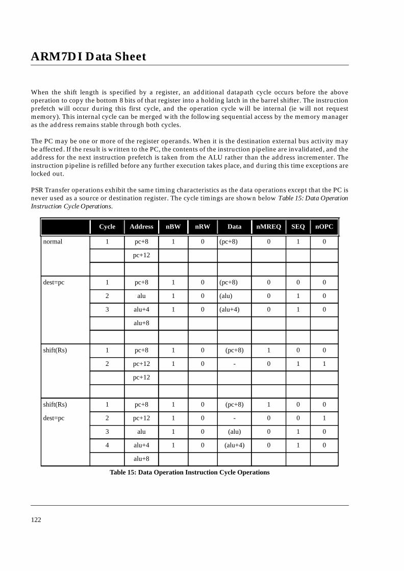
ARM7DI Data Sheet
122
When the shift length is specified by a register, an additional datapath cycle occurs before the aboveoperation to copy the bottom 8 bits of that register into a holding latch in the barrel shifter. The instructionprefetch will occur during this first cycle, and the operation cycle will be internal (ie will not requestmemory). This internal cycle can be merged with the following sequential access by the memory manageras the address remains stable through both cycles.
The PC may be one or more of the register operands. When it is the destination external bus activity maybe affected. If the result is written to the PC, the contents of the instruction pipeline are invalidated, and theaddress for the next instruction prefetch is taken from the ALU rather than the address incrementer. Theinstruction pipeline is refilled before any further execution takes place, and during this time exceptions arelocked out.
PSR Transfer operations exhibit the same timing characteristics as the data operations except that the PC isnever used as a source or destination register. The cycle timings are shown below Table 15: Data OperationInstruction Cycle Operations.
Cycle Address nBW nRW Data nMREQ SEQ nOPC
normal 1 pc+8 1 0 (pc+8) 0 1 0
pc+12
dest=pc 1 pc+8 1 0 (pc+8) 0 0 0
2 alu 1 0 (alu) 0 1 0
3 alu+4 1 0 (alu+4) 0 1 0
alu+8
shift(Rs) 1 pc+8 1 0 (pc+8) 1 0 0
2 pc+12 1 0 - 0 1 1
pc+12
shift(Rs) 1 pc+8 1 0 (pc+8) 1 0 0
dest=pc 2 pc+12 1 0 - 0 0 1
3 alu 1 0 (alu) 0 1 0
4 alu+4 1 0 (alu+4) 0 1 0
alu+8
Table 15: Data Operation Instruction Cycle Operations

Instruction Cycle Operations
123
9.3 Multiply and multiply accumulate
The multiply instructions make use of special hardware which implements a 2 bit Booth's algorithm withearly termination. During the first cycle the accumulate Register is brought to the ALU, which eithertransmits it or produces zero (depending on the instruction being MLA or MUL) to initialise the destinationregister. During the same cycle, the multiplier (Rs) is loaded into the Booth's shifter via the A bus.
The datapath then cycles, adding the multiplicand (Rm) to, subtracting it from, or just transmitting, theresult register. The multiplicand is shifted in the Nth cycle by 2N or 2N+1 bits, under control of the Booth'slogic. The multiplier is shifted right 2 bits per cycle, and when it is zero the instruction terminates (possiblyafter an additional cycle to clear a pending borrow).
All cycles except the first are internal. The cycle timings are shown below in Table 16: Multiply InstructionCycle Operations.
m is the number of cycles required by the Booth's algorithm; see the section on instruction speeds.
9.4 Load register
The first cycle of a load register instruction performs the address calculation. The data is fetched frommemory during the second cycle, and the base register modification is performed during this cycle (ifrequired). During the third cycle the data is transferred to the destination register, and external memory isunused. This third cycle may normally be merged with the following prefetch to form one memory N-cycle.The cycle timings are shown below in Table 17: Load Register Instruction Cycle Operations.
Cycle Address nBW nRW Data nMREQ SEQ nOPC
(Rs)=0,1 1 pc+8 1 0 (pc+8) 1 0 0
2 pc+12 1 0 - 0 1 1
pc+12 (pc+8)
(Rs)>1 1 pc+8 1 0 (pc+8) 1 0 0
2 pc+12 1 0 - 1 0 1
• pc+12 1 0 - 1 0 1
m pc+12 1 0 - 1 0 1
m+1 pc+12 1 0 - 0 1 1
pc+12
Table 16: Multiply Instruction Cycle Operations

ARM7DI Data Sheet
124
Either the base or the destination (or both) may be the PC, and the prefetch sequence will be changed if thePC is affected by the instruction.
The data fetch may abort, and in this case the destination modification is prevented.
9.5 Store register
The first cycle of a store register is similar to the first cycle of load register. During the second cycle the basemodification is performed, and at the same time the data is written to memory. There is no third cycle. Thecycle timings are shown below in Table 18: Store Register Instruction Cycle Operations.
Cycle Address nBW nRW Data nMREQ SEQ nOPC
normal 1 pc+8 1 0 (pc+8) 0 0 0
2 alu b/w 0 (alu) 1 0 1
3 pc+12 1 0 - 0 1 1
pc+12
dest=pc 1 pc+8 1 0 (pc+8) 0 0 0
2 alu b/w 0 pc’ 1 0 1
3 pc+12 1 0 - 0 0 1
4 pc’ 1 0 (pc’) 0 1 0
5 pc’+4 1 0 (pc’+4) 0 1 0
pc’+8
Table 17: Load Register Instruction Cycle Operations
Cycle Address nBW nRW Data nMREQ SEQ nOPC
1 pc+8 1 0 (pc+8) 0 0 0
2 alu b/w 1 Rd 0 0 1
pc+12
Table 18: Store Register Instruction Cycle Operations

Instruction Cycle Operations
125
9.6 Load multiple registers
The first cycle of LDM is used to calculate the address of the first word to be transferred, whilst performinga prefetch from memory. The second cycle fetches the first word, and performs the base modification.During the third cycle, the first word is moved to the appropriate destination register while the secondword is fetched from memory, and the modified base is latched internally in case it is needed to patch upafter an abort. The third cycle is repeated for subsequent fetches until the last data word has been accessed,then the final (internal) cycle moves the last word to its destination register. The cycle timings are shown inTable 19: Load Multiple Registers Instruction Cycle Operations.
The last cycle may be merged with the next instruction prefetch to form a single memory N-cycle.
If an abort occurs, the instruction continues to completion, but all register writing after the abort isprevented. The final cycle is altered to restore the modified base register (which may have been overwrittenby the load activity before the abort occurred).
When the PC is in the list of registers to be loaded the current instruction pipeline must be invalidated.
Note that the PC is always the last register to be loaded, so an abort at any point will prevent the PC frombeing overwritten.

ARM7DI Data Sheet
126
Cycle Address nBW nRW Data nMREQ SEQ nOPC
1 register 1 pc+8 1 0 (pc+8) 0 0 0
2 alu 1 0 (alu) 1 0 1
3 pc+12 1 0 - 0 1 1
pc+12
1 register 1 pc+8 1 0 (pc+8) 0 0 0
dest=pc 2 alu 1 0 pc’ 1 0 1
3 pc+12 1 0 - 0 0 1
4 pc’ 1 0 (pc’) 0 1 0
5 pc’+4 1 0 (pc’+4) 0 1 0
pc’+8
n registers 1 pc+8 1 0 (pc+8) 0 0 0
(n>1) 2 alu 1 0 (alu) 0 1 1
• alu+• 1 0 (alu+•) 0 1 1
n alu+• 1 0 (alu+•) 0 1 1
n+1 alu+• 1 0 (alu+•) 1 0 1
n+2 pc+12 1 0 - 0 1 1
pc+12
n registers 1 pc+8 1 0 (pc+8) 0 0 0
(n>1) 2 alu 1 0 (alu) 0 1 1
incl pc • alu+• 1 0 (alu+•) 0 1 1
n alu+• 1 0 (alu+•) 0 1 1
n+1 alu+• 1 0 pc’ 1 0 1
n+2 pc+12 1 0 - 0 0 1
n+3 pc’ 1 0 (pc’) 0 1 0
n+4 pc’+4 1 0 (pc’+4) 0 1 0
pc’+8
Table 19: Load Multiple Registers Instruction Cycle Operations

Instruction Cycle Operations
127
9.7 Store multiple registers
Store multiple proceeds very much as load multiple, without the final cycle. The restart problem is muchmore straightforward here, as there is no wholesale overwriting of registers to contend with. The cycletimings are shown in Table 20: Store Multiple Registers Instruction Cycle Operations.
9.8 Data swap
This is similar to the load and store register instructions, but the actual swap takes place in cycles 2 and 3.In the second cycle, the data is fetched from external memory. In the third cycle, the contents of the sourceregister are written out to the external memory. The data read in cycle 2 is written into the destinationregister during the fourth cycle. The cycle timings are shown below in Table 21: Data Swap Instruction CycleOperations.
The LOCK output of ARM7DI is driven HIGH for the duration of the swap operation (cycles 2 & 3) toindicate that both cycles should be allowed to complete without interruption.
The data swapped may be a byte or word quantity (b/w).
The swap operation may be aborted in either the read or write cycle, and in both cases the destinationregister will not be affected.
Cycle Address nBW nRW Data nMREQ SEQ nOPC
1 register 1 pc+8 1 0 (pc+8) 0 0 0
2 alu 1 1 Ra 0 0 1
pc+12
n registers 1 pc+8 1 0 (pc+8) 0 0 0
(n>1) 2 alu 1 1 Ra 0 1 1
• alu+• 1 1 R• 0 1 1
n alu+• 1 1 R• 0 1 1
n+1 alu+• 1 1 R• 0 0 1
pc+12
Table 20: Store Multiple Registers Instruction Cycle Operations

ARM7DI Data Sheet
128
9.9 Software interrupt and exception entry
Exceptions (and software interrupts) force the PC to a particular value and refill the instruction pipelinefrom there. During the first cycle the forced address is constructed, and a mode change may take place. Thereturn address is moved to R14 and the CPSR to SPSR_svc.
During the second cycle the return address is modified to facilitate return, though this modification is lessuseful than in the case of branch with link.
The third cycle is required only to complete the refilling of the instruction pipeline. The cycle timings areshown below in Table 22: Software Interrupt Instruction Cycle Operations.
where C represents the current mode-dependent value.
For software interrupts, pc is the address of the SWI instruction. For interrupts and reset, pc is the addressof the instruction following the last one to be executed before entering the exception. For prefetch abort, pcis the address of the aborting instruction. For data abort, pc is the address of the instruction following theone which attempted the aborted data transfer. Xn is the appropriate trap address.
Cycle Address nBW nRW Data nMREQ SEQ nOPC LOCK
1 pc+8 1 0 (pc+8) 0 0 0 0
2 Rn b/w 0 (Rn) 0 0 1 1
3 Rn b/w 1 Rm 1 0 1 1
4 pc+12 1 0 - 0 1 1 0
pc+12
Table 21: Data Swap Instruction Cycle Operations
Cycle Address nBW nRW Data nMREQ SEQ nOPC nTRANS Mode
1 pc+8 1 0 (pc+8) 0 0 0 C old mode
2 Xn 1 0 (Xn) 0 1 0 1 exceptionmode
3 Xn+4 1 0 (Xn+4) 0 1 0 1 exceptionmode
Xn+8
Table 22: Software Interrupt Instruction Cycle Operations

Instruction Cycle Operations
129
9.10 Coprocessor data operation
A coprocessor data operation is a request from ARM7DI for the coprocessor to initiate some action. Theaction need not be completed for some time, but the coprocessor must commit to doing it before drivingCPB LOW.
If the coprocessor can never do the requested task, it should leave CPA and CPB HIGH. If it can do the task,but can't commit right now, it should drive CPA LOW but leave CPB HIGH until it can commit. ARM7DIwill busy-wait until CPB goes LOW. The cycle timings are shown in Table 23: Coprocessor Data OperationInstruction Cycle Operations.
9.11 Coprocessor data transfer (from memory to coprocessor)
Here the coprocessor should commit to the transfer only when it is ready to accept the data. When CPB goesLOW, ARM7DI will produce addresses and expect the coprocessor to take the data at sequential cycle rates.The coprocessor is responsible for determining the number of words to be transferred, and indicates the lasttransfer cycle by driving CPA and CPB HIGH.
ARM7DI spends the first cycle (and any busy-wait cycles) generating the transfer address, and performsthe write-back of the address base during the transfer cycles. The cycle timings are shown in Table 24:Coprocessor Data Transfer Instruction Cycle Operations.
Cycle Address nBW nRW Data nMREQ SEQ nOPC nCPI CPA CPB
ready 1 pc+8 1 0 (pc+8) 0 0 0 0 0 0
pc+12
not ready 1 pc+8 1 0 (pc+8) 1 0 0 0 0 1
2 pc+8 1 0 - 1 0 1 0 0 1
• pc+8 1 0 - 1 0 1 0 0 1
n pc+8 1 0 - 0 0 1 0 0 0
pc+12
Table 23:Coprocessor Data Operation Instruction Cycle Operations

ARM7DI Data Sheet
130
Cycle Address nBW nRW Data nMREQ SEQ nOPC nCPI CPA CPB
1 register 1 pc+8 1 0 (pc+8) 0 0 0 0 0 0
ready 2 alu 1 0 (alu) 0 0 1 1 1 1
pc+12
1 register 1 pc+8 1 0 (pc+8) 1 0 0 0 0 1
not ready 2 pc+8 1 0 - 1 0 1 0 0 1
• pc+8 1 0 - 1 0 1 0 0 1
n pc+8 1 0 - 0 0 1 0 0 0
n+1 alu 1 0 (alu) 0 0 1 1 1 1
pc+12
n registers 1 pc+8 1 0 (pc+8) 0 0 0 0 0 0
(n>1) 2 alu 1 0 (alu) 0 1 1 1 0 0
ready • alu+• 1 0 (alu+•) 0 1 1 1 0 0
n alu+• 1 0 (alu+•) 0 1 1 1 0 0
n+1 alu+• 1 0 (alu+•) 0 0 1 1 1 1
pc+12
m registers 1 pc+8 1 0 (pc+8) 1 0 0 0 0 1
(m>1) 2 pc+8 1 0 - 1 0 1 0 0 1
not ready • pc+8 1 0 - 1 0 1 0 0 1
n pc+8 1 0 - 0 0 1 0 0 0
n+1 alu 1 0 (alu) 0 1 1 1 0 0
• alu+• 1 0 (alu+•) 0 1 1 1 0 0
n+m alu+• 1 0 (alu+•) 0 1 1 1 0 0
n+m+1 alu+• 1 0 (alu+•) 0 0 1 1 1 1
pc+12
Table 24: Coprocessor Data Transfer Instruction Cycle Operations

Instruction Cycle Operations
131
9.12 Coprocessor data transfer (from coprocessor to memory)
The ARM7DI controls these instructions exactly as for memory to coprocessor transfers, with the oneexception that the nRW line is inverted during the transfer cycle. The cycle timings are show in Table 25:Coprocessor Data Transfer Instruction Cycle Operations.
Cycle Address nBW nRW Data nMREQ SEQ nOPC nCPI CPA CPB
1 register 1 pc+8 1 0 (pc+8) 0 0 0 0 0 0
ready 2 alu 1 1 CPdata 0 0 1 1 1 1
pc+12
1 register 1 pc+8 1 0 (pc+8) 1 0 0 0 0 1
not ready 2 pc+8 1 0 - 1 0 1 0 0 1
• pc+8 1 0 - 1 0 1 0 0 1
n pc+8 1 0 - 0 0 1 0 0 0
n+1 alu 1 1 CPdata 0 0 1 1 1 1
pc+12
n registers 1 pc+8 1 0 (pc+8) 0 0 0 0 0 0
(n>1) 2 alu 1 1 CPdata 0 1 1 1 0 0
ready • alu+• 1 1 CPdata 0 1 1 1 0 0
n alu+• 1 1 CPdata 0 1 1 1 0 0
n+1 alu+• 1 1 CPdata 0 0 1 1 1 1
pc+12
m registers 1 pc+8 1 0 (pc+8) 1 0 0 0 0 1
(m>1) 2 pc+8 1 0 - 1 0 1 0 0 1
not ready • pc+8 1 0 - 1 0 1 0 0 1
n pc+8 1 0 - 0 0 1 0 0 0
n+1 alu 1 1 CPdata 0 1 1 1 0 0
• alu+• 1 1 CPdata 0 1 1 1 0 0
n+m alu+• 1 1 CPdata 0 1 1 1 0 0
n+m+1 alu+• 1 1 CPdata 0 0 1 1 1 1
pc+12
Table 25: Coprocessor Data Transfer Instruction Cycle Operations

ARM7DI Data Sheet
132
9.13 Coprocessor register transfer (Load from coprocessor)
Here the busy-wait cycles are much as above, but the transfer is limited to one data word, and ARM7DIputs the word into the destination register in the third cycle. The third cycle may be merged with thefollowing prefetch cycle into one memory N-cycle as with all ARM7DI register load instructions. The cycletimings are shown in Table 26: Coprocessor register transfer (Load from coprocessor).
9.14 Coprocessor register transfer (Store to coprocessor)
As for the load from coprocessor, except that the last cycle is omitted. The cycle timings are shown belowin Table 27: Coprocessor register transfer (Store to coprocessor).
Cycle Address nBW nRW Data nMREQ SEQ nOPC nCPI CPA CPB
ready 1 pc+8 1 0 (pc+8) 1 1 0 0 0 0
2 pc+12 1 0 CPdata 1 0 1 1 1 1
3 pc+12 1 0 - 0 1 1 1 - -
pc+12
not ready 1 pc+8 1 0 (pc+8) 1 0 0 0 0 1
2 pc+8 1 0 CPdata 1 0 1 0 0 1
• pc+8 1 0 - 1 0 1 0 0 1
n pc+8 1 0 - 1 1 1 0 0 0
n+1 pc+12 1 0 CPdata 1 0 1 1 1 1
n+2 pc+12 1 0 - 0 1 1 1 - -
pc+12
Table 26: Coprocessor register transfer (Load from coprocessor)

Instruction Cycle Operations
133
9.15 Undefined instructions and coprocessor absent
When a coprocessor detects a coprocessor instruction which it cannot perform, and this must include allundefined instructions, it must not drive CPA or CPB LOW. These will remain HIGH, causing theundefined instruction trap to be taken. Cycle timings are shown in Table 28: Undefined Instruction CycleOperations.
Cycle Address nBW nRW Data nMREQ SEQ nOPC nCPI CPA CPB
ready 1 pc+8 1 0 (pc+8) 1 1 0 0 0 0
2 pc+12 1 1 Rd 0 0 1 1 1 1
pc+12
not ready 1 pc+8 1 0 (pc+8) 1 0 0 0 0 1
2 pc+8 1 0 - 1 0 1 0 0 1
• pc+8 1 0 - 1 0 1 0 0 1
n pc+8 1 0 - 1 1 1 0 0 0
n+1 pc+12 1 1 Rd 0 0 1 1 1 1
pc+12
Table 27: Coprocessor register transfer (Store to coprocessor)
Cycle Address nBW nRW Data nMREQ SEQ nOPC nCPI CPA CPB nTRANS Mode
1 pc+8 1 0 (pc+8) 1 0 0 0 1 1 Old Old
2 pc+8 1 0 - 0 0 0 1 1 1 Old Old
3 Xn 1 0 (Xn) 0 1 0 1 1 1 1 00100
4 Xn+4 1 0 (Xn+4) 0 1 0 1 1 1 1 00100
Xn+8
Table 28: Undefined Instruction Cycle Operations

ARM7DI Data Sheet
134
9.16 Unexecuted instructions
Any instruction whose condition code is not met will fail to execute. It will add one cycle to the executiontime of the code segment in which it is embedded (see Table 29: Unexecuted Instruction Cycle Operations).
9.17 Instruction Speed Summary
Due to the pipelined architecture of the CPU, instructions overlap considerably. In a typical cycle oneinstruction may be using the data path while the next is being decoded and the one after that is beingfetched. For this reason the following table presents the incremental number of cycles required by aninstruction, rather than the total number of cycles for which the instruction uses part of the processor.Elapsed time (in cycles) for a routine may be calculated from these figures which are shown in Table 30:ARM Instruction Speed Summary. These figures assume that the instruction is actually executed. Unexecutedinstructions take one cycle.
Cycle Address nBW nRW Data nMREQ SEQ nOPC
1 pc+8 1 0 (pc+8) 0 1 0
pc+12
Table 29: Unexecuted Instruction Cycle Operations
Instruction Cycle count Additional
Data Processing 1S + 1I for SHIFT(Rs)+ 1S + 1N if R15 written
MSR, MRS 1S
LDR 1S + 1N + 1I + 1S + 1N if R15 loaded
STR 2N
LDM nS + 1N + 1I + 1S + 1N if R15 loaded
STM (n-1)S + 2N
SWP 1S + 2N + 1I
B,BL 2S + 1N
SWI, trap 2S + 1N
MUL,MLA 1S + mI
CDP 1S + bI
LDC,STC (n-1)S + 2N + bI
MCR 1N + bI + 1C
MRC 1S + (b+1)I + 1C
Table 30: ARM Instruction Speed Summary

Instruction Cycle Operations
135
n is the number of words transferred.
m is the number of cycles required by the multiply algorithm, which is determined by the contents ofRs. Multiplication by any number between 2^(2m-3) and 2^(2m-1)-1 takes 1S+mI m cycles for1<m>16. Multiplication by 0 or 1 takes 1S+1I cycles, and multiplication by any number greater thanor equal to 2^(29) takes 1S+16I cycles. The maximum time for any multiply is thus 1S+16I cycles.
b is the number of cycles spent in the coprocessor busy-wait loop.
If the condition is not met all the instructions take one S-cycle. The cycle types N, S, I, and C are defined inChapter 5.0 Memory Interface.

ARM7DI Data Sheet
136

DC Parameters
137
10.0 DC Parameters
*Subject to Change*
10.1 Absolute Maximum Ratings
Note:
These are stress ratings only. Exceeding the absolute maximum ratings may permanently damage thedevice. Operating the device at absolute maximum ratings for extended periods may affect devicereliability.
10.2 DC Operating Conditions:
Notes:
1. Voltages measured with respect to VSS.
2. IC CMOS-level inputs
Symbol Parameter Min Max Units Note
VDD Supply voltage VSS-0.3 VSS+7.0 V 1
Vin Input voltage applied to any pin VSS-0.3 VDD+0.3 V 1
Ts Storage temperature -40 125 deg C 1
Table 31: ARM7DI DC Maximum Ratings
Symbol Parameter Min Typ Max Units Notes
VDD Supply voltage 2.7 3.0 - 5.0 5.5 V
Vihc IC input HIGH voltage .8xVDD VDD V 1,2
Vilc IC input LOW voltage 0.0 .2xVDD V 1,2
Ta Ambient operating temperature 0 70 ¡C
Table 32: ARM7DI DC Operating Conditions

ARM7DI Data Sheet
138

AC Parameters
139
11.0 AC Parameters
*** Important Note - Provisional Figures ***
The timing parameters given here are preliminary data and subject to change.
The AC timing diagrams presented in this section assume that the outputs of the ARM7DI have been loadedwith the capacitive loads shown in the `Test Load' column of Table 33: AC Test Loads. These loads have beenchosen as typical of the type of system in which ARM7DI might be employed.
The output drivers of the ARM7DI are CMOS inverters which exhibit a propagation delay that increaseslinearly with the increase in load capacitance. An “Output derating” figure is given for each output driver,showing the approximate rate of increase of output time with increasing load capacitance.
OutputSignal
TestLoad(pF)
Outputderating(ns/pF)
D[31:0] TBD TBD
A[31:0] TBD TBD
LOCK TBD TBD
nCPI TBD TBD
nMREQ TBD TBD
SEQ TBD TBD
nRW TBD TBD
nBW TBD TBD
nOPC TBD TBD
nTRANS TBD TBD
TDO TBD TBD
Table 33: AC Test Loads

ARM7DI Data Sheet
140
Figure 53: General Timings
Note: nWAIT and ABE are both HIGH during the cycle shown. Tcdel is the delay (on either edge) fromMCLK changing to ECLK changing.
MCLK
ECLK
A[31:0]
nRW
nBW,LOCK
nTRANS
nOPC
nMREQ,SEQ
nEXEC
Tcdel Tcdel
TahTaddr
TrwhTrwd
TblhTbld
TmdhTmdd
TopchTopcd
TmshTmsd
TexhTexd

AC Parameters
141
Figure 54: Address Timing
Note: Tald is the time by which ALE must be driven LOW in order to latch the current address in phase2. If ALE is driven low after Tald, then a new address will be latched.
Figure 55: Address Control
Figure 56: Data Write Cycle
Note: DBE is HIGH and nENIN is LOW during the cycle shown.
MCLK
ALE
A[31:0]nRW, nBWLOCK, nOPCnTRANS
Tald
Tale
MCLK
ABE
A[31:0]nRW, nBWLOCK, nOPCnTRANS Tabz
TabeTaddr
MCLK
nENOUT
D[31:0]
Tnen
Tdout Tdoh

ARM7DI Data Sheet
142
Figure 57: Data Read Cycle
Note: DBE is HIGH and nENIN is LOW during the cycle shown.
Figure 58: Data Bus Control
Note: The cycle shown is a data write cycle since nENOUT was driven LOW during phase 1. Here, DBEhas first been used to modify the behaviour of the data bus, and then nENIN.
MCLK
nENOUT
D[31:0]
Tnen
Tdis Tdih
MCLK
nENOUT
DBE
D[31:0]
nENIN
Tdbnen Tdbnen
Tdbz Tdbe
Tdout Tdoh
TdbzTdbe

AC Parameters
143
Figure 59: Output 3-state Time
Figure 60: Configuration Pin Timing
Figure 61: Coprocessor Timing
Note: Normally, nMREQ and SEQ become valid Tmsd after the falling edge of MCLK. In this cycle theARM has been busy-waiting, waiting for a coprocessor to complete the instruction. If CPA and CPBchange during phase 1, the timing of nMREQ and SEQ will depend on Tcpms. Most systemsshould be able to generate CPA and CPB during the previous phase 2, and so the timing of nMREQand SEQ will always be Tmsd.
MCLK
TBE
A[31:0]D[31:0]nRW, nBWLOCK, nOPCnTRANS
TtbzTtbe
MCLK
BIGEND,DATA32,PROG32,ISYNC Tcth Tcts
MCLK
nCPI
CPA, CPB
nMREQ,SEQ
Tcpi Tcpih
TcpsTcph
Tcpms

ARM7DI Data Sheet
144
Figure 62: Exception Timing
Note: Tirs guarantees recognition of the interrupt (or reset) source by the corresponding clock edge. Tirmguarantees non-recognition by that clock edge. These inputs may be applied fully asynchronouslywhere the exact cycle of recognition is unimportant.
Figure 63: Debug Timing
MCLK
ABORT
nRESET
nFIQ, nIRQ
Tabts Tabth
Tirs Tirm
Tirs Tirm
MCLK
DBGACK
BREAKPT
DBGRQ
EXTERN[1:0]
TdbghTdbgd
Tbrks Tbrkh
Trqs Trqh
Texts Texth

AC Parameters
145
Figure 64: TCK-ECLK relationship
Figure 65: MCLK Timing
Note: The ARM core is not clocked by the HIGH phase of MCLK enveloped by nWAIT. Thus, during thecycles shown, nMREQ and SEQ change once, during the first LOW phase of MCLK, and A[31:0]change once, during the second HIGH phase of MCLK. For reference, ph2 is shown. This is theinternal clock from which the core times all its activity. This signal is included to show how the highphase of the external MCLK has been removed from the internal core clock.
11.0.1 Notes on AC Parameters
All figures are provisional, and assume that 0.8 micron CMOS technology is used to fabricate theARM7DI.
TCK
ECLK
Tctdel Tctdel
MCLK
nWAIT
ECLK
nMREQ/SEQ
A[31:0]
Tclkl Tclkh
Tws Twh
Tmsd
Taddr
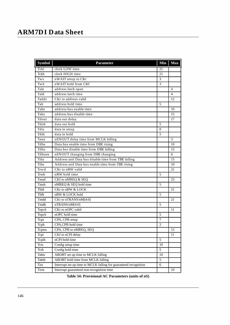
ARM7DI Data Sheet
146
Symbol Parameter Min Max
Tckl clock LOW time 21Tckh clock HIGH time 21Tws nWAIT setup to CKr 3Twh nWAIT hold from CKf 3Tale address latch open 4
Tald address latch time 4Taddr CKr to address valid 12Tah address hold time 5Tabe address bus enable time 10
Tabz address bus disable time 15
Tdout data out delay 17
Tdoh data out hold 5
Tdis data in setup 0
Tdih data in hold 5
Tnen nENOUT delay time from MCLK falling 3
Tdbe Data bus enable time from DBE rising 10
Tdbz Data bus disable time from DBE falling 15
Tdbnen nENOUT changing from DBE changing 6
Ttbz Address and Data bus disable time from TBE falling 15
Ttbe Address and Data bus enable time from TBE rising 10
Trwd CKr to nRW valid 21
Trwh nRW hold time 5
Tmsd CKf to nMREQ & SEQ 23
Tmsh nMREQ & SEQ hold time 5
Tbld CKr to nBW & LOCK 21
Tblh nBW & LOCK hold 5
Tmdd CKr to nTRANS/nM[4:0] 21
Tmdh nTRANS/nM[4:0] 5
Topcd CKr to nOPC valid 11
Topch nOPC hold time 5
Tcps CPA, CPB setup 7
Tcph CPA,CPB hold time 2
Tcpms CPA, CPB to nMREQ, SEQ 15
Tcpi CKf to nCPI delay 11
Tcpih nCPI hold time 5
Tcts Config setup time 10
Tcth Config hold time 5
Tabts ABORT set up time to MCLK falling 10
Tabth ABORT hold time from MCLK falling 5
Tirs Interrupt set up time to MCLK falling for guaranteed recognition 6
Tirm Interrupt guaranteed non-recognition time 10
Table 34: Provisional AC Parameters (units of nS)

AC Parameters
147
Texd MCLK falling to nEXEC valid 21
Texh nEXEC hold time from MCLK falling 5Tbrks Set up time of BREAKPT to MCLK rising 10Tbrkh Hold time of BREAKPT from MCLK rising 5Tdbgd MCLK rising to DBGACK valid 5Tdbgh DGBACK hold time from MCLK rising 3Trqs DBGRQ set up time to MCLK falling for guaranteed recognition 6Trqh DBGRQ guaranteed non-recognition time 10Tcdel MCLK to ECLK delay 4Tctdel TCK to ECLK delay 4
Texts EXTERN[1:0] set up time to MCLK falling 5Texth EXTERN[1:0] hold time from MCLK falling 5
Symbol Parameter Min Max
Table 34: Provisional AC Parameters (units of nS)

ARM7DI Data Sheet
148

Appendix - Backward Compatibility
149
12.0 Appendix - Backward Compatibility
Two inputs, PROG32 and DATA32, allow one of three processor configurations to be selected as follows:
(1) 26 bit program and data space - (PROG32 LOW, DATA32 LOW). This configuration forcesARM7DI to operate like the earlier ARM processors with 26 bit address space. The programmer'smodel for these processors applies, but the new instructions to access the CPSR and SPSR registersoperate as detailed elsewhere in this document. In this configuration it is impossible to select a 32bit operating mode, and all exceptions (including address exceptions) enter the exception handlerin the appropriate 26 bit mode.
(2) 26 bit program space and 32 bit data space - (PROG32 LOW, DATA32 HIGH). This is the same asthe 26 bit program and data space configuration, but with address exceptions disabled to allowdata transfer operations to access the full 32 bit address space.
(3) 32 bit program and data space - (PROG32 HIGH, DATA32 HIGH). This configuration extends theaddress space to 32 bits, introduces major changes in the programmer's model as described belowand provides support for running existing 26 bit programs in the 32 bit environment.
The fourth processor configuration which is possible (26 bit data space and 32 bit program space) shouldnot be selected.
When configured for 26 bit program space, ARM7DI is limited to operating in one of four modes known asthe 26 bit modes. These modes correspond to the modes of the earlier ARM processors and are known as:
User26
FIQ26
IRQ26 and
Supervisor26.
These are the normal operating modes in this configuration and the 26 bit modes are only provided forbackwards compatibility to allow execution of programs originally written for earlier ARM processors.
The differences between ARM7DI and the earlier ARM processors are documented in an ARM ApplicationNote 11 - “Differences between ARM6 and earlier ARM Processors”

ARM7DI Data Sheet
150