department of computer science and engineering … notes.pdfdepartment of computer science and...
TRANSCRIPT

CS2354 – ADVANCED COMPUTER ARCHITECTURE
SCAD ENGINEERING COLLEGE,DEPARTMENT OF CSE
SCAD ENGINEERING COLLEGE
DEPARTMENT OF COMPUTER SCIENCE AND
ENGINEERING
CS 2354- ADVANCED COMPUTER
ARCHITECTURE
REGULATION 2008
FOR
SIXTH SEMESTER
COMPUTER SCIENCE AND ENGINEERING

CS2354 – ADVANCED COMPUTER ARCHITECTURE
SCAD ENGINEERING COLLEGE,DEPARTMENT OF CSE
UNIT I
INSTRUCTION LEVEL PARALLELISM
ILP – Concepts and challenges – Hardware and software approaches – Dynamic scheduling – Speculation - Compiler techniques for exposing ILP – Branch prediction.
PART-B
1. Explain the data dependences and hazards in detail with examples. (16)
Data Dependences and Hazards
If two instructions are parallel, they can execute simultaneously in a pipeline of arbitrary depth
without causing any stalls, assuming the pipeline has sufficient resources (and hence no
structural hazards exist). If two instructions are dependent, they are not parallel and must be
executed in order, although they may often be partially overlapped. The key in both cases is to
determine whether an instruction is dependent on another instruction.
Data Dependences
There are three different types of dependences:
Data dependences (also called true data dependences)
Name dependences(also called anti dependence)
Control dependences.
An instruction j is data dependent on instruction i if either of the following holds:
Instruction i produces a result that may be used by instruction j. Instruction j is data dependent
on instruction k, and instruction k is data dependent on instruction i
The second condition simply states that one instruction is dependent on another if there exists a chain of
dependences of the first type between the two instructions. This dependence chain can be as long as the
entire program. Note that dependence within a single instruction (such as ADDD R1.R1.R1) is not
considered dependence.
Loop: L.D F0,0(R1)
ADD.D F4 ,F0,F2
S.D F4,0(R1)

CS2354 – ADVANCED COMPUTER ARCHITECTURE
SCAD ENGINEERING COLLEGE,DEPARTMENT OF CSE
Explanation:
Both of the above dependent sequences, as shown by the arrows, have each instruction
depending on the previous one. The arrows here and in above examples show the order
that must be preserved for correct execution.
The arrow points from an instruction that must precede the instruction that the
arrowhead points to. If two instructions are data dependent, they cannot execute
simultaneously or be completely overlapped. The dependence implies that there would
be a chain of one or more data hazards between the two instruction
Name Dependences
The second type of dependence is name dependence. Name dependence occurs when two instructions
use the same register or memory location, called a name, but there is no flow of data between the
instructions associated with that name. There are two types of name dependences between an
instruction i that precedes instruction j in program order
1. An anti dependence between instruction i and instruction j occurs when instruction j writes a
register or memory location that instruction i reads. The original ordering must be preserved
to ensure that i reads the correct value. In the example on page 69, there is an anti
dependence between S. D and DADDIU on register Rl.
2. An output dependence occurs when instruction i and instruction j write the same register or
memory location. The ordering between the instructions must be preserved to ensure that the
value finally written corresponds to instruction j.
Example:
InstrJ writes operand before InstrI writes it.
I: sub r1,r4,r3
J: add r1,r2,r3
K: mul r6,r1,r7
Called an ―output dependence‖ by compiler writers. This also results from the reuse of name ―r1‖
Data Hazards
A hazard is created whenever there is a dependence between instructions, and they are close enough
that the overlap during execution would change the order of access to the operand involved in the
dependence. Because of the dependence, we must preserve what is called program order, that is, the

CS2354 – ADVANCED COMPUTER ARCHITECTURE
SCAD ENGINEERING COLLEGE,DEPARTMENT OF CSE
order that the instructions would execute in if executed sequentially one at a time as determined by the
original source program. The goal of both our software and hardware techniques is to exploit parallelism
by preserving program order only where it affects the out-come of the program. Detecting and avoiding
hazards ensures that necessary program order is preserved.
RAW (read after write) —j tries to read a source before i writes it, so j incorrectly gets the old
value. This hazard is the most common type and corresponds to a true data dependence. Program
order must be preserved to ensure that j receives the value from i.
WAW (write after write) —j tries to write an operand before it is written by i. The writes end up
being performed in the wrong order, leaving the value written by i rather than the value written
by j in the destination. This hazard corresponds to an output dependence. WAW hazards are
present only in pipelines that write in more than one pipe stage or allow an instruction to
proceed even when a previous instruction is stalled.
WAR (write after read)—j tries to write a destination before it is read by i, so i incorrectly gets
the new value. This hazard arises from an anti dependence. WAR hazards cannot occur in
most static issue pipelines—even deeper pipelines or floating-point pipelines—because all reads
are early (in ID) and all writes are late (in WB).
Example: for WAR Hazard: Floating-point data part
Loop: L.D F0, 0(R1) ;F0=array element
ADD.D F4, F0, F2 ;add scalar in F2
S.D F4, 0(R1) ;store result
Integer data part
DADDUI R1, R1, #-8 ;decrement pointer
;8 bytes (per DW)
BNE R1, R2, Loop ;branch R1!=R2
Control Dependences
A control dependence determines the ordering of an instruction, i, with respect to a branch
instruction so that the instruction i is executed in correct program order and only when it should be.
Every instruction, except for those in the first basic block of the program, is control dependent on some
set of branches, and, in general, these control dependences must be preserved to preserve program order.
if P1 {
S1; };

CS2354 – ADVANCED COMPUTER ARCHITECTURE
SCAD ENGINEERING COLLEGE,DEPARTMENT OF CSE
if P2 {
S2; }
S1 is control dependent on p1, and S2 is control dependent on p2 but not on p1. In general, there are two
constraints imposed by control dependences:
1. An instruction that is control dependent on a branch cannot be moved before the branch so that its
execution is no longer controlled by the branch. For example, we cannot take an instruction from the
then portion of an if statement and move it before the if statement.
2. An instruction that is not control dependent on a branch cannot be moved after the branch so that its
execution is controlled by the branch. For example, we cannot take a statement before the if statement
and move it into the then portion.
2. Briefly explain the concept of dynamic scheduling. (8)
Dynamic scheduling
A major limitation of simple pipelining techniques is that they use in-order instruction issue and
execution: Instructions are issued in program order, and if an instruction is stalled in the
pipeline, no later instructions can proceed.
Thus, if there is a dependence between two closely spaced instructions in the pipeline, this will
lead to a hazard and a stall will result. If there are multiple functional units, these units could lie
idle. If instruction j depends on a long-running instruction i, currently in execution in the
pipeline, then all instructions after j must be stalled until i is finished and 7 can execute.
For example, consider this code:
DIV.D F0,F2,F4
ADD.D F10,F0,F8
SUB.D F12,F8,F14
The SUB.D instruction cannot execute because the dependence of ADD.D on DIV.D causes the
pipeline to stall; yet SUB. D is not data dependent on anything in the pipeline.
This hazard creates a performance limitation that can be eliminated by not requiring instructions
to execute in program order. In the classic five-stage pipeline, both structural and data hazards
could be checked during instruction decode (ID): When an instruction could execute without
hazards, it was issued from ID knowing that all data hazards had been resolved.
To allow us to begin executing the SUB. D in the above example, we must separate the issue
process into two parts: checking for any structural hazards and waiting for the absence of a data
hazard. Thus, we still use in-order instruction issue (i.e., instructions issued in program order),

CS2354 – ADVANCED COMPUTER ARCHITECTURE
SCAD ENGINEERING COLLEGE,DEPARTMENT OF CSE
but we want an instruction to begin execution as soon as its data operands are available. Such a
pipeline does out-of-order execution, which implies out-of-order completion.
Out-of-order execution introduces the possibility of WAR and WAW hazards, which do not exist in the
five-stage integer pipeline and its logical extension to an in-order floating-point pipeline. Consider the
following MIPS floating-point code sequence:
DIV.D F0,F2,F4
ADD.D F6,F0,F8
SUB.D F8,F10,F14
MUL.D F6,F10,F8
There is an antidependence between the ADD. D and the SUB.D, and if the pipeline executes the
SUB. D before the ADD. D (which is waiting for the DIV. D), it will violate the antidependence,
yielding a WAR hazard. Likewise, to avoid violating output dependences, such as the write of
F6 by MUL.D, WAW hazards must be handled. As we will see, both these hazards are avoided
by the use of register renaming.
Out-of-order completion also creates major complications in handling exceptions. Dynamic
scheduling with out-of-order completion must preserve exception behavior in the sense that
exactly those exceptions that would arise if the program were executed in strict program order
actually do arise.
Dynamically scheduled processors preserve exception behavior by ensuring that no instruction
can generate an exception until the processor knows that the instruction raising the exception
will be executed; we will see shortly how this property can be guaranteed.
Although exception behavior must be preserved, dynamically scheduled processors may
generate imprecise exceptions. An exception is imprecise if the processor state when an
exception is raised does not look exactly as if the instructions were executed sequentially in
strict program order. Imprecise exceptions can occur because of two possibilities:
1. The pipeline may have already completed instructions that are later in pro-gram order
than the instruction causing the exception.
2. The pipeline may have not yet completed some instructions that are earlier in program
order than the instruction causing the exception. Imprecise exceptions make it difficult to
restart execution after an exception. Rather than address these problems in this section, we
will discuss a solution that provides precise exceptions in the context of a processor with
speculation To allow out-of-order execution, we essentially split the ID pipe stage of our
simple five-stage pipeline into two stages:
Issue—Decode instructions, check for structural hazards.
Read operands—Wait until no data hazards, then read operands.

CS2354 – ADVANCED COMPUTER ARCHITECTURE
SCAD ENGINEERING COLLEGE,DEPARTMENT OF CSE
We distinguish when an instruction begins execution and when it completes execution; between the two
times, the instruction is in execution. Our pipeline allows multiple instructions to be in execution at the
same time, and without this capability, a major advantage of dynamic scheduling is lost. Having multiple
instructions in execution at once requires multiple functional units, pipelined functional units, or both.
In a dynamically scheduled pipeline, all instructions pass through the issue stage in order (in-order
issue); however, they can be stalled or bypass each other in the second stage (read operands) and thus
enter execution out of order.
3. Explain dynamic scheduling using tomosulo’s approach with an
example. (or) explain technique used for overcoming the data
hazards with an example.
RAW hazards are avoided by executing an instruction only when its operands are
available.
WAR and WAW hazards, which arise from name dependences, are eliminated by register
renaming. Register renaming eliminates these hazards by renaming all destination
registers, including those with a pending read or write for an earlier instruction, so that
the out-of-order write does not affect any instructions that depend on an earlier value of an
operand.
To better understand how register renaming eliminates WAR and WAW hazards, consider the following
example code sequence that includes both a potential WAR and WAW hazard:
DIV.D F0.F2.F4
ADD.D F6,F0,F8
S.D F6,0(R1)
SUB.D F8,F10,F14
MUL.D F6,F10,F8
There is an antidependence between the ADD.D and the SUB.D and an output dependence between the
ADD.D and the MilL.D, leading to two possible hazards: a WAR hazard on the use of F8 by ADD. D
and a WAW hazard since the ADD. D may finish later than the MUL.D. There are also three true data
dependences: between the DIV.D and the ADD.D, between the SUB.D and the MUL.D, and between the
ADD.D and the S.D.

CS2354 – ADVANCED COMPUTER ARCHITECTURE
SCAD ENGINEERING COLLEGE,DEPARTMENT OF CSE
These two name dependences can both be eliminated by register renaming. For simplicity, assume the
existence of two temporary registers, S and T. Using S and T, the sequence can be rewritten without any
dependences as
DIV.D F0,F2,F4
ADD.D S,F0,F8
S.D S,0(R1)
SUB.D T.F10.F14
MUL.D F6,F10,T
In addition, any subsequent uses of F8 must be replaced by the register T. In this code segment,
the renaming process can be done statically by the compiler. Finding any uses of F8 that are later
in the code requires either sophisticated compiler analysis or hardware support, since there may
be intervening branches between the above code segment and a later use of F8.
In Tomasulo's scheme, register renaming is provided by reservation stations which buffer the
operands of instructions waiting to issue. The basic idea is that a reservation station fetches and
buffers an operand as soon as it is available, eliminating the need to get the operand from a
register.
In addition, pending instructions designate the reservation station that will provide their input.
Finally, when successive writes to a register overlap in execution, only the last one is actually
used to update the register. As instructions are issued, the register specifiers for pending
operands are renamed to the names of the reservation station, which provides register renaming.
Since there can be more reservation stations than real registers, the technique can even eliminate
hazards arising from name dependences that could not be eliminated by a compiler.
USE OF RESERVATION STATIONS:
The use of reservation stations, rather than a centralized register file, leads to two other
important properties. First, hazard detection and execution control are distributed: The
information held in the reservation stations at each functional unit determine when an instruction
can begin execution at that unit.
Second, results are passed directly to functional units from the reservation stations where they
are buffered, rather than going through the registers. This bypassing is done with a common
result bus that allows all units waiting for an operand to be loaded simultaneously (on the 360/91
this is called the common data bus, or CDB). In pipelines with multiple execution units and
issuing multiple instructions per clock, more than one result bus will be needed.

CS2354 – ADVANCED COMPUTER ARCHITECTURE
SCAD ENGINEERING COLLEGE,DEPARTMENT OF CSE
The basic structure of a Tomasulo-based processor, including both the floating-point unit and the load-
store unit; none of the execution control tables are shown.
COMPONENTS OF TOMOSULO’S ARCHITECTURE:
RESERVATION STATION:
Each reservation station holds an instruction that has been issued and is awaiting execution at a
functional unit, and either the operand values for that instruction, if they have already been
computed, or else the names of the reservation stations that will provide the operand values.
The load buffers and store buffers hold data or addresses coming from and going to memory and
behave almost exactly like reservation stations, so we distinguish them only when necessary.
The floating-point registers are connected by a pair of buses to the functional units and by a
single bus to the store buffers.
RESERVATION STATION COMPONENTS:
Op: operation to perform in the unit (e.g., + or –)
Vj, Vk: value of Source operands
o Store buffers has V field, result to be stored
Qj, Qk: reservation stations producing source registers (value to be written)

CS2354 – ADVANCED COMPUTER ARCHITECTURE
SCAD ENGINEERING COLLEGE,DEPARTMENT OF CSE
o Note: Qj,Qk=0 => ready
o Store buffers only have Qi for RS producing result
Busy: indicates reservation station or FU is busy
Register result status: Indicates which functional unit will write each register, if one exists.
Blank when no pending instructions that will write that register.
Steps an involved in tomosulo algorithm. There are only three steps, although each one can now take an
arbitrary number of clock cycles:
Issue—Get the next instruction from the head of the instruction queue, which is maintained in
FIFO order to ensure the maintenance of correct data flow. If there is a matching reservation
station that is empty, issue the instruction to the station with the operand values, if they are
currently in the registers. If there is not an empty reservation station, then there is a structural
hazard and the instruction stalls until a station or buffer is freed. If the operands are not in the
registers, keep track of the functional units that will produce the operands. This step renames
registers, eliminating WAR and WAW hazards. (This stage is sometimes called dispatch in a
dynamically scheduled processor.)
Execute—If one or more of the operands is not yet available, monitor the common data bus
while waiting for it to be computed. When an operand becomes available, it is placed into any
reservation station awaiting it. When all the operands are available, the operation can be
executed at the corresponding functional unit. By delaying instruction execution until the
operands are available, RAW hazards are avoided. (Some dynamically scheduled processors call
this step "issue," but we use the name "execute," which was used in the first dynamically
scheduled processor, the CDC 6600.)
o Loads and stores require a two-step execution process. The first step computes the
effective address when the base register is available, and the effective address is then
placed in the load or store buffer. Loads in the load buffer execute as soon as the
memory unit is available. Stores in the store buffer wait for the value to be stored before
being sent to the memory unit.
Write result—When the result is available, write it on the CDB and from there into the registers
and into any reservation stations (including store buffers) waiting for this result. Stores are
buffered in the store buffer until both the value to be stored and the store address are available,
then the result is written as soon as the memory unit is free.
Instruction status: Exec Write
Instruction j k Issue Comp Result Busy Address
LD F6 34+ R2 1 3 4 Load1 No
LD F2 45+ R3 2 4 5 Load2 No
MULTD F0 F2 F4 3 15 16 Load3 No
SUBD F8 F6 F2 4 7 8
DIVD F10 F0 F6 5 56 57
ADDD F6 F8 F2 6 10 11
Reservation Stations: S1 S2 RS RS
Time Name Busy Op Vj Vk Qj Qk
Add1 No
Add2 No
Add3 No
Mult1 No
Mult2 Yes DIVD M*F4 M(A1)
Register result status:
Clock F0 F2 F4 F6 F8 F10 F12 ... F3056 FU M*F4 M(A2) (M-M+M)(M-M) Result
CS2354 – ADVANCED COMPUTER ARCHITECTURE
SCAD ENGINEERING COLLEGE,DEPARTMENT OF CSE

CS2354 – ADVANCED COMPUTER ARCHITECTURE
SCAD ENGINEERING COLLEGE,DEPARTMENT OF CSE
4. Explain in detail about the hardware based speculation and explain
how it overcomes the control dependencies. (16)
Hardware-based speculation combines three key ideas:
Dynamic branch prediction to choose which instructions to execute
Speculation to allow the execution of instructions before the control dependences are
resolved (with the ability to undo the effects of an incorrectly speculated sequence)
Dynamic scheduling to deal with the scheduling of different combinations of basic blocks.
Hardware-based speculation follows the predicted flow of data values to choose when to execute
instructions. This method of executing programs is essentially a data flow execution: Operations
execute as soon as their operands are available.
Role of commit stage:
Using the bypassed value is like performing a speculative register read, since we do not know whether
the instruction providing the source register value is providing the correct result until the instruction is
no longer speculative. When an instruction is no longer speculative, we allow it to update the register
file or memory we call this additional step in the instruction execution sequence instruction commit.
KEY IDEA BEHIND HARDWARE SPECULATION:
The key idea behind implementing speculation is to allow instructions to execute out of order
but to force them to commit in order and to prevent any irrevocable action (such as updating
state or taking an exception) until an instruction commits.
Hence, when we add speculation, we need to separate the process of completing execution from
instruction commit, since instructions may finish execution considerably before they are ready to
commit. Adding this commit phase to the instruction execution sequence requires an additional
set of hardware buffers that hold the results of instructions that have finished execution but have
not committed. This hardware buffer, which we call the reorder buffer, is also used to pass
results among instructions that may be speculated.
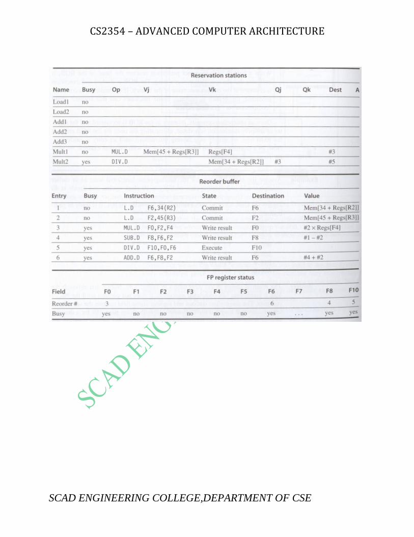
ROLE OF RE-ORDER BUFFER:
The reorder buffer (ROB) provides additional registers in the same way as the reservation
stations in Tomasulo's algorithm extend the register set. The ROB holds the result of an
instruction between the time the operation associated with the instruction completes and
the time the instruction commits. Hence, the ROB is a source of operands for instructions, just
as the reservation stations provide operands in Tomasulo's algorithm.
The key difference is that in Tomasulo's algorithm, once an instruction writes its result, any
subsequently issued instructions will find the result in the register file.

CS2354 – ADVANCED COMPUTER ARCHITECTURE
SCAD ENGINEERING COLLEGE,DEPARTMENT OF CSE
With speculation, the register file is not updated until the instruction commits (and we know
definitively that the instruction should execute); thus, the ROB supplies operands in the interval
between completion of instruction execution and instruction commit.
Each entry in the ROB contains four fields:
Instruction type
o The instruction type field indicates whether the instruction is a branch (and
has no destination result), a store (which has a memory address destination),
or a register operation (ALU operation or load, which has register
destinations).
Destination field
o The destination field supplies the register number (for loads and ALU
operations) or the memory address (for stores) where the instruction result
should be written.
Value field
o The value field is used to hold the value of the instruction result until the
instruction commits.
Ready field.
o The ready field indicates that the instruction has completed execution, and
the value is ready.

CS2354 – ADVANCED COMPUTER ARCHITECTURE
SCAD ENGINEERING COLLEGE,DEPARTMENT OF CSE
Here are the four steps involved in instruction execution:
1. Issue—Get an instruction from the instruction queue. Issue the instruction if there is an empty
reservation station and an empty slot in the ROB; send the operands to the reservation station if they are
available in either the registers or the ROB. Update the control entries to indicate the buffers are in use.
The number of the ROB entry allocated for the result is also sent to the reservation station, so that the
number can be used to tag the result when it is placed on the CDB. If either all reservations are full or
the ROB is full, then instruction issue is stalled until both have available entries.
2. Execute—If one or more of the operands is not yet available, monitor the CDB while waiting for the
register to be computed. This step checks for RAW hazards. When both operands are available at a
reservation station, execute the operation. Instructions may take multiple clock cycles in this stage, and
loads still require two steps in this stage. Stores need only have the base register available at this step,
since execution for a store at this point is only effective address calculation.
3. Write result—When the result is available, write it on the CDB (with the ROB tag sent when the
instruction issued) and from the CDB into the ROB, as well as to any reservation stations waiting for

CS2354 – ADVANCED COMPUTER ARCHITECTURE
SCAD ENGINEERING COLLEGE,DEPARTMENT OF CSE
this result. Mark the reservation station as available. Special actions are required for store instructions. If
the value to be stored is available, it is written into the Value field of the ROB entry for the store. If the
value to be stored is not available yet, the CDB must be monitored until that value is broadcast, at which
time the Value field of the ROB entry of the store is updated. For simplicity we assume that this occurs
during the Write Results stage of a store; we discuss relaxing this requirement later.
4. Commit—This is the final stage of completing an instruction, after which only its result remains.
(Some processors call this commit phase "completion" or "graduation.") There are three different
sequences of actions at commit depending on whether the committing instruction is a branch with an
incorrect prediction, a store, or any other instruction (normal commit).
The normal commit case occurs when an instruction reaches the head of the ROB and its
result is present in the buffer; at this point, the processor updates the register with the
result and removes the instruction from the ROB.
When a branch with incorrect prediction reaches the head of the ROB, it indicates that
the speculation was wrong. The ROB is flushed and execution is restarted at the correct
successor of the branch. If the branch was correctly predicted, the branch is finished.
CS2354 – ADVANCED COMPUTER ARCHITECTURE
SCAD ENGINEERING COLLEGE,DEPARTMENT OF CSE

CS2354 – ADVANCED COMPUTER ARCHITECTURE
SCAD ENGINEERING COLLEGE,DEPARTMENT OF CSE
5. Explain the basic compiler techniques for exposing ilp. (8)
Basic Pipeline Scheduling and Loop Unrolling
To keep a pipeline full, parallelism among instructions must be exploited by finding sequences
of unrelated instructions that can be overlapped in the pipeline.
To avoid a pipeline stall, a dependent instruction must be separated from the source instruction
by a distance in clock cycles equal to the pipeline latency of that source instruction.
Consider the following code segment, which adds a scalar to a vector:
for (i = 1000; i>0; i =i-1)
x[i] = x[i] + s;
We can see that this loop is parallel by noticing that the body of each iteration is independent. First, let's
look at the performance of this loop, showing how we can use the parallelism to improve its
performance for a MIPS pipeline with the latencies shown above.
Instruction producing result Instruction using result Latency in clock cycles
FP ALU op Another FP ALU op 3
FP ALU op Store double 2
Load double FP ALU op 1
Load double Store double 0
The first step is to translate the above segment to MIPS assembly language. In the following code
segment, Rl is initially the address of the element in the array with the highest address, and F2 contains
the scalar value s. Register R2 is precompiled, so that 8(R2) is the address of the last element to operate
on.
The straightforward MIPS code, not scheduled for the pipeline, looks like this:
Loop: L.D FO,O(R1) ;F0=array element
ADD.D F4,F0,F2 ;add scalar in F2
S.D F4,0(R1) ;store result
CS2354 – ADVANCED COMPUTER ARCHITECTURE
SCAD ENGINEERING COLLEGE,DEPARTMENT OF CSE
DADDUI Rl,Rl,#-8 ;decrement pointer
;8 bytes (per DW)
BNE Rl,R2,Loop ;branch R1!=R2
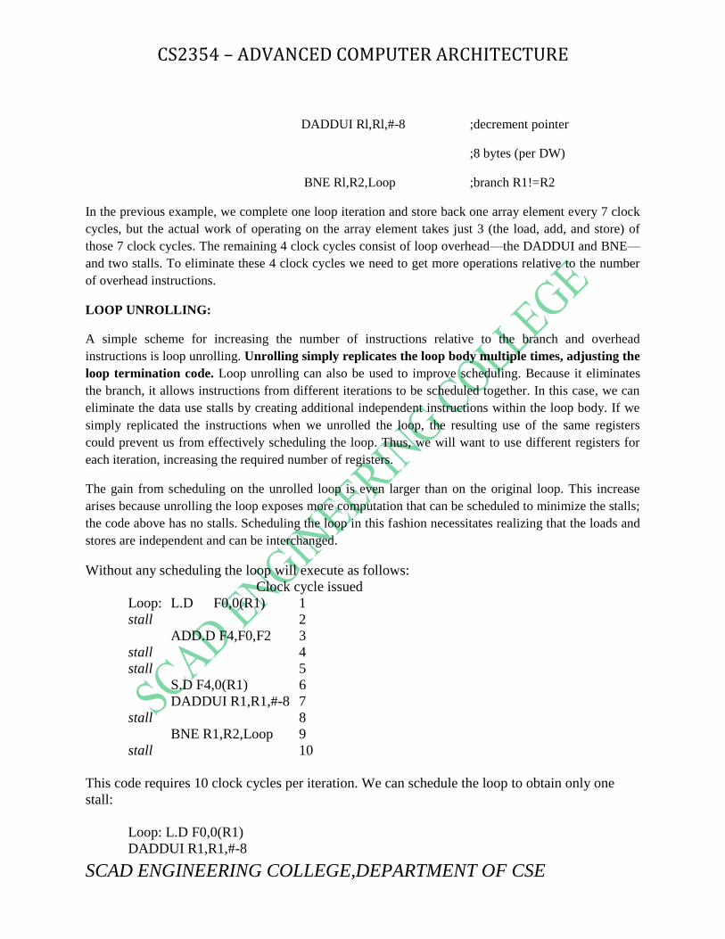
In the previous example, we complete one loop iteration and store back one array element every 7 clock
cycles, but the actual work of operating on the array element takes just 3 (the load, add, and store) of
those 7 clock cycles. The remaining 4 clock cycles consist of loop overhead—the DADDUI and BNE—
and two stalls. To eliminate these 4 clock cycles we need to get more operations relative to the number
of overhead instructions.
LOOP UNROLLING:
A simple scheme for increasing the number of instructions relative to the branch and overhead
instructions is loop unrolling. Unrolling simply replicates the loop body multiple times, adjusting the
loop termination code. Loop unrolling can also be used to improve scheduling. Because it eliminates
the branch, it allows instructions from different iterations to be scheduled together. In this case, we can
eliminate the data use stalls by creating additional independent instructions within the loop body. If we
simply replicated the instructions when we unrolled the loop, the resulting use of the same registers
could prevent us from effectively scheduling the loop. Thus, we will want to use different registers for
each iteration, increasing the required number of registers.
The gain from scheduling on the unrolled loop is even larger than on the original loop. This increase
arises because unrolling the loop exposes more computation that can be scheduled to minimize the stalls;
the code above has no stalls. Scheduling the loop in this fashion necessitates realizing that the loads and
stores are independent and can be interchanged.
Without any scheduling the loop will execute as follows:
Clock cycle issued
Loop: L.D F0,0(R1) 1
stall 2
ADD.D F4,F0,F2 3
stall 4
stall 5
S.D F4,0(R1) 6
DADDUI R1,R1,#-8 7
stall 8
BNE R1,R2,Loop 9
stall 10
This code requires 10 clock cycles per iteration. We can schedule the loop to obtain only one
stall:
Loop: L.D F0,0(R1)
DADDUI R1,R1,#-8

CS2354 – ADVANCED COMPUTER ARCHITECTURE
SCAD ENGINEERING COLLEGE,DEPARTMENT OF CSE
ADD.D F4,F0,F2
stall
BNE R1,R2,Loop ; delayed branch
S.D F4,8(R1) ; altered & interchanged with DADDUI
Execution time has been reduced from 10 clock cycles to 6. The stall after ADD.D is for the use
by the S.D.
WITH UNROLLING:
Loop: L.D F0,0(R1)
L.D F6,-8(R1)
L.D F10,-16(R1)
L.D F14,-24(R1)
ADD.D F4,F0,F2
ADD.D F8,F6,F2
ADD.D F12,F10,F2
ADD.D F16,F14,F2
S.D F4,0(R1)
S.D F8,-8(R1)
DADDUI R1,R1,#-32
S.D F12,16(R1)
BNE R1,R2,Loop
S.D F16,8(R1) ;8-32 = -24
6. Explain static and dynamic branch prediction schemes (16)
Static Branch Prediction
The behavior of branches can be predicted both statically at compile time and dynamically by the
hardware at execution time. Static branch predictors are sometimes used in processors where the
expectation is that branch behavior is highly predictable at compile time; static prediction can also be
used to assist dynamic predictors.
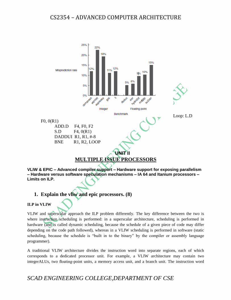
The simplest scheme is to predict a branch as taken. This scheme has an average misprediction rate that
is equal to the untaken branch frequency, which for the SPEC programs is 34%. Unfortunately, the
misprediction rate for the SPEC programs ranges from not very accurate (59%) to highly accurate (9%).
A more accurate technique is to predict branches on the basis of profile information collected from
earlier runs. The key observation that makes this worth while is that the behavior of branches is often
bimodally distributed that is, an individual branch is often highly biased toward taken or untaken.
Dynamic Branch Prediction and Branch-Prediction Buffers
The simplest dynamic branch-prediction scheme is a branch-prediction buffer or branch history table. A
branch-prediction buffer is a small memory indexed by the lower portion of the address of the branch

CS2354 – ADVANCED COMPUTER ARCHITECTURE
SCAD ENGINEERING COLLEGE,DEPARTMENT OF CSE
instruction. The memory contains a bit that says whether the branch was recently taken or not. This
scheme is the simplest sort of buffer; it has no tags and is useful only to reduce the branch delay when it
is longer than the time to compute the possible target PCs. With such a buffer, we don't know, in fact, if
the prediction is correct—it may have been put there by another branch that has the same low-order
address bits.
But this doesn't matter. The prediction is a hint that is assumed to be correct, and fetching begins
in the predicted direction. If the hint turns out to be wrong, the prediction bit is inverted and
stored back.
This simple 1-bit prediction scheme ---- has a performance shortcoming: Even if a branch is almost
always taken,
we will likely
predict
incorrectly
twice, rather
than once,
when it is not
taken, since
the misprediction
causes the
prediction bit
to be flipped.
To remedy this
weakness, 2-
bit prediction
schemes are often used. In a 2-bit scheme, a prediction must miss twice before it is changed. Figure
shows the finite-state processor for a 2-bit prediction scheme.
CS2354 – ADVANCED COMPUTER ARCHITECTURE
SCAD ENGINEERING COLLEGE,DEPARTMENT OF CSE
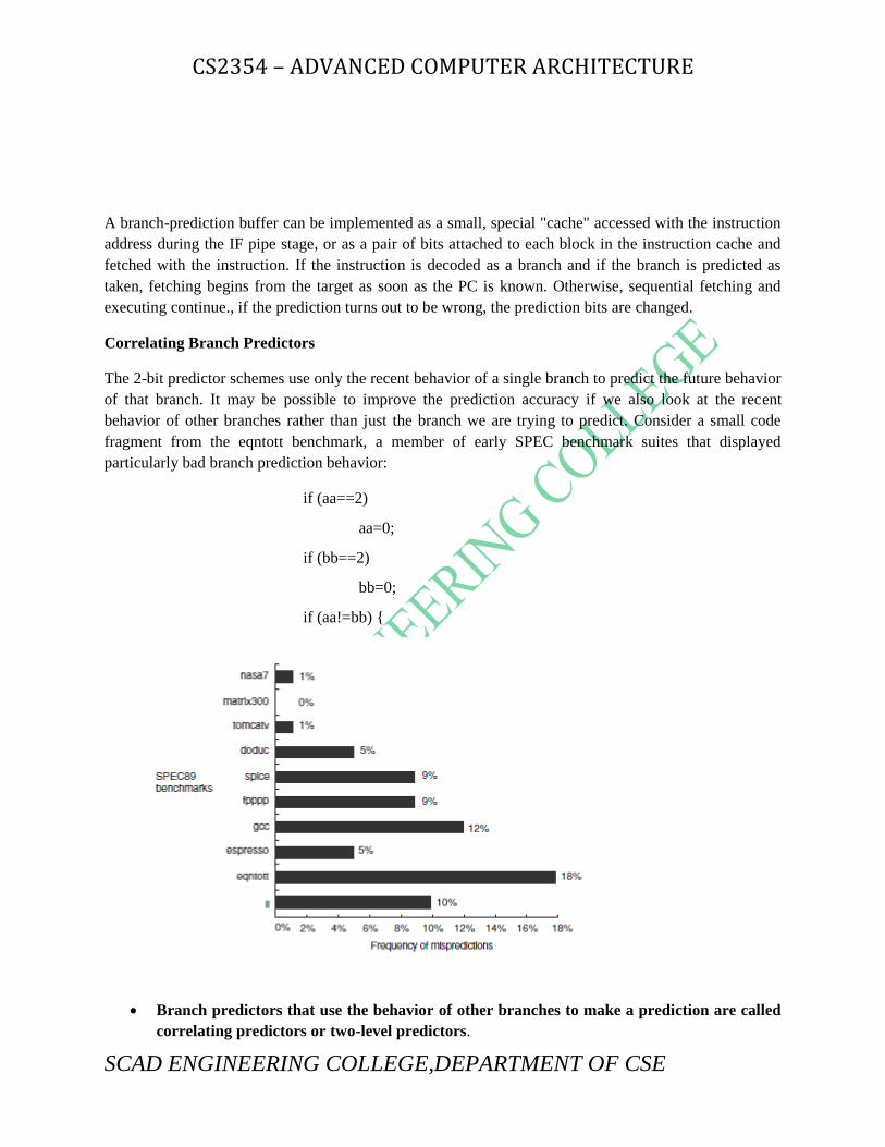
A branch-prediction buffer can be implemented as a small, special "cache" accessed with the instruction
address during the IF pipe stage, or as a pair of bits attached to each block in the instruction cache and
fetched with the instruction. If the instruction is decoded as a branch and if the branch is predicted as
taken, fetching begins from the target as soon as the PC is known. Otherwise, sequential fetching and
executing continue., if the prediction turns out to be wrong, the prediction bits are changed.
Correlating Branch Predictors
The 2-bit predictor schemes use only the recent behavior of a single branch to predict the future behavior
of that branch. It may be possible to improve the prediction accuracy if we also look at the recent
behavior of other branches rather than just the branch we are trying to predict. Consider a small code
fragment from the eqntott benchmark, a member of early SPEC benchmark suites that displayed
particularly bad branch prediction behavior:
if (aa==2)
aa=0;
if (bb==2)
bb=0;
if (aa!=bb) {
Branch predictors that use the behavior of other branches to make a prediction are called
correlating predictors or two-level predictors.

CS2354 – ADVANCED COMPUTER ARCHITECTURE
SCAD ENGINEERING COLLEGE,DEPARTMENT OF CSE
Existing correlating predictors add information about the behavior of the most recent branches to
decide how to predict a given branch. For example, a (1,2) predictor uses the behavior of the last
branch to choose from among a pair of 2-bit branch predictors in predicting a particular branch.
In the general case an (m,n) predictor uses the behavior of the last m branches to choose from
2m branch predictors, each of which is an n-bit predictor for a single branch. The attraction of
this type of correlating branch predictor is that it can yield higher prediction rates than the 2-bit
scheme and requires only a trivial amount of additional hardware.
Tournament Predictors: Adaptively Combining Local and Global Predictors
The primary motivation for correlating branch predictors came from the observation that the standard 2-
bit predictor using only local information failed on some important branches and that, by adding global
information, the performance could be improved. Tournament predictors take this insight to the next
level, by using multiple predictors, usually one based on global information and one based on local
information, and combining them with a selector.
Tournament predictors can achieve both better accuracy at medium sizes (8K-32K bits) and also make
use of very large numbers of prediction bits effectively. Existing tournament predictors use a 2-bit
saturating counter per branch to choose among two different predictors based on which predictor (local,
global, or even some mix) was most effective in recent predictions. As in a simple 2-bit predictor, the
saturating counter requires two mispredictions before changing the identity of the preferred predictor.
The advantage of a tournament predictor is its ability to select the right predictor for a particular branch,
which is particularly crucial for the integer benchmarks. A typical tournament predictor will select the
global predictor almost 40% of the time for the SPEC integer benchmarks and less than 15% of the time
for the SPEC FP benchmarks.

CS2354 – ADVANCED COMPUTER ARCHITECTURE
SCAD ENGINEERING COLLEGE,DEPARTMENT OF CSE
The above figure looks at the performance of three different predictors (a local 2-bit predictor, a
correlating predictor, and a tournament predictor) for different numbers of bits using SPEC89 as the
benchmark. As we saw earlier, the prediction capability of the local predictor does not improve beyond a
certain size. The correlating predictor shows a significant improvement, and the tournament predictor
generates slightly better performance. For more recent versions of the SPEC, the results would be
similar, but the asymptotic behavior would not be reached until slightly larger-sized predictors.

CS2354 – ADVANCED COMPUTER ARCHITECTURE
SCAD ENGINEERING COLLEGE,DEPARTMENT OF CSE
UNIT-I
PART-A 1. Explain the concept of pipelining.
Pipelining is an implementation technique whereby multiple instructions are overlapped
in execution. It takes advantage of parallelism that exists among actions needed to
execute an instruction.
2. What is a Hazard? Mention the different hazards in pipeline.
Hazards are situations that prevent the next instruction in the instruction stream from
executing during its designated clock cycle. Hazards reduce the overall performance from
the ideal speedup gained by pipelining. The three classes of hazards are,
i) Structural hazard
ii) Data hazard
iii) Control hazard
3. List the various dependences.
Data dependence
Name dependence
Control dependence
4. What is Instruction Level Parallelism? (or) What is ILP?
Pipelining is used to overlap the execution of instructions and improve performance. This
potential overlap among instructions is called instruction level parallelism (ILP) since
instruction can be evaluated parallel.
5. Give an example of control dependence.
If p1 { s1;}
If p2 {s2;}
S1 is control dependence on p1, and s2 is control dependence on p2.
6. Write the concept behind using reservation station.
Reservation station fetches and buffers an operand as soon as available, eliminating the
need to get the operand from a register.
7. Explain the idea behind dynamic scheduling? Also write advantages of dynamic
scheduling.
In dynamic scheduling the hardware rearranges the instruction to reduce the stalls while
maintaining dataflow and exception behavior.
Advantages: it enables handling some cases when dependence are unknown at compile
time and it simplifies the compiler. It allows code that was compiled with one pipeline in
mind and run efficiently on a different pipeline.
8. What are the possibilities of imprecise exception?

CS2354 – ADVANCED COMPUTER ARCHITECTURE
SCAD ENGINEERING COLLEGE,DEPARTMENT OF CSE
The pipeline may have already completed instructions that are later in program order than
instruction causing exception. The pipeline may have not yet completed some
instructions that ere earlier in program order than the instructions causing exception.
9. What are branch target buffers?
To reduce the branch penalty we need to know from what address to fetch by end of
Instruction fetch. A branch prediction cache that stores the predicted address for the next
instruction after a branch is called a branch-target buffer or branch target cache.
10. Mention the idea behind hardware-based speculation?
It combines three key ideas:
Dynamic branch prediction to choose which instruction to execute,
Speculation to allow the execution of instructions before control dependence are resolved
Dynamic scheduling to deal with the scheduling of different combinations of basic
blocks.
11. What are the fields in the ROB?
Instruction type, destination field, value field and ready field.
The advantage
of tournament predictor is its ability to select the right predictor for right branch.
12. What is loop unrolling?
A simple scheme for increasing the number of instructions relative to the branch and
overhead instructions is loop unrolling. Unrolling simply replicates the loop body
multiple times, adjusting the loop termination code.
13. What are the basic compiler techniques?
Loop unrolling, Code scheduling.
CS2354 – ADVANCED COMPUTER ARCHITECTURE
SCAD ENGINEERING COLLEGE,DEPARTMENT OF CSE
Loop: L.D
F0, 0(R1)
ADD.D F4, F0, F2
S.D F4, 0(R1)
DADDUI R1, R1, #-8
BNE R1, R2, LOOP
UNIT II MULTIPLE ISSUE PROCESSORS
VLIW & EPIC – Advanced compiler support – Hardware support for exposing parallelism – Hardware versus software speculation mechanisms – IA 64 and Itanium processors – Limits on ILP.
1. Explain the vliw and epic processors. (8)
ILP in VLIW
VLIW and superscalar approach the ILP problem differently. The key difference between the two is
where instruction scheduling is performed: in a superscalar architecture, scheduling is performed in
hardware (and is called dynamic scheduling, because the schedule of a given piece of code may differ
depending on the code path followed), whereas in a VLIW scheduling is performed in software (static
scheduling, because the schedule is ―built in to the binary‖ by the compiler or assembly language
programmer).
A traditional VLIW architecture divides the instruction word into separate regions, each of which
corresponds to a dedicated processor unit. For example, a VLIW architecture may contain two
integerALUs, two floating-point units, a memory access unit, and a branch unit. The instruction word

CS2354 – ADVANCED COMPUTER ARCHITECTURE
SCAD ENGINEERING COLLEGE,DEPARTMENT OF CSE
may then be divided into an integer portion, a floating-point portion, a memory load/store portion, and a
branch portion.
The downside is that writing a good compiler for a VLIW is much more difficult than for a
superscalar architecture, and the difference between a good compiler and a bad one is far more
noticeable.
Another problem with traditional VLIW is code size. Often it is simply not possible to
completely utilize all processor execution units at once. Thus many instructions contain no-ops
in portions of the instruction word with a corresponding increase in the size of the object code.
Increased code size has obvious implications for the efficacy of caches and bus bandwidth.
Modern VLIWs deal with this problem in different ways. One simple method is to offer several
instruction templates, and allow the compiler to pick the most appropriate one – in this case, the
one that utilises the most bits of the instruction word.
In a VLIW the obvious solution is, however, to increase the length of instruction word. This obvious
solution has similarly-obvious compatibility problems. Another alternative is to add more instructions to
the instruction word, making use of the extra processing unit without causing compatibility problems.
EPIC ARCHITECTURE
The EPIC architecture is based on VLIW, but was designed to overcome the key limitations of VLIW (in
particular,hardware dependence) while simultaneously giving more flexibility to compiler writers. So far
the only implementation of this architecture is as part of the IA-64 processor architecture in the Itanium
family of processors.
Instruction-level parallelism in EPIC
Crucially, the length of a bundle does not define the limits of parallelism; the bundle template
type indicates, by the presence or absence of a stop, whether instructions following the bundle
can execute in parallel with instructions in the bundle. The claim of EPIC is that as the processor
family evolves, processors with greater support for parallelism will simply issue more bundles
simultaneously.
The first 4 bundles all contain memory (M) and integer ALU (I) mini-instructions. higher-
numbered bundles contain different types of mini-instructions. Template 0 contains one memory
and two integer instructions and no stops, meaning that a sequence of template-0 bundles will be
executed in parallel as much as the hardware is capable, whereas template 1 contains a stop after
the second integer instruction but is otherwise identical. The hardware ensures that all instructions
before the stop have been retired before executing instructions after the stop.
For example, all current Itaniums issue two bundles at a time through a technique known as
dispersal. The first part of a bundle is issued, and then the bundle is logically shifted so that the

CS2354 – ADVANCED COMPUTER ARCHITECTURE
SCAD ENGINEERING COLLEGE,DEPARTMENT OF CSE
next part of the bundle is available for execution. If the mini-instruction cannot be executed, split
issue occurs.
The bundle continues to occupy its bundle slot, and another bundle is loaded to occupy the next
slot. Since some instructions from the bundle have been executed, leaving them in the bundle slot
reduces parallelism
Static Multiple Issue : The VLIW Approach
The compiler may be required to ensure that dependences within the issue packet cannot be
present or, at a minimum, indicate when dependence may be present.
The first multiple-issue processors that required the instruction stream to be explicitly organized
to avoid dependences. This architectural approach was named VLIW, standing for Very Long
Instruction Word, and denoting that the instructions, since they contained several instructions,
were very wide (64 to 128 bits, or more).
The basic architectural concepts and compiler technology are the same whether multiple
operations are organized into a single instruction, or whether a set of instructions in an issue
packet is preconfigured by a compiler to exclude dependent operations (since the issue packet can
be thought of as a very large instruction).
The Basic VLIW Approach
VLIWs use multiple, independent functional units. Rather than attempting to issue multiple,
independent instructions to the units, a VLIW packages the multiple operations into one very long
instruction, or requires that the instructions in the issue packet satisfy the same constraints.
For example, a VLIW processor might have instructions that contain five operations, including:
one integer operation (which could also be a branch), two floating-point operations, and two
memory references. The instruction would have a set of fields for each functional unit— perhaps
16 to 24 bits per unit, yielding an instruction length of between 112 and 168 bits.
To keep the functional units busy, there must be enough parallelism in a code sequence to fill the
available operation slots. This parallelism is uncovered by unrolling loops and scheduling the
code within the single larger loop body. If the unrolling generates straight line code, then local
scheduling techniques, which operate on a single basic block can be used. If finding and
exploiting the parallelism requires scheduling code across branches, a substantially more complex
global scheduling algorithm must be used.

CS2354 – ADVANCED COMPUTER ARCHITECTURE
SCAD ENGINEERING COLLEGE,DEPARTMENT OF CSE
2. Explain hardware support for compilers for exposing ilp. (16)
Why Hardware Support:
Techniques such as loop unrolling, software pipelining, and trace scheduling can be used to
increase the amount of parallelism available when the behavior of branches is fairly predictable at
compile time. When the behavior of branches is not well known, compiler techniques alone may not be
able to uncover much ILP. In such cases, the control dependences may severely limit the amount of
parallelism that can be exploited.
Hardware speculation with in-order commit preserved exception behavior by detecting and
raising exceptions only at commit time when the instruction was no longer speculative. To
enhance the ability of the compiler to speculatively move code over branches, while still
preserving the exception behavior, we consider several different methods, which either include

CS2354 – ADVANCED COMPUTER ARCHITECTURE
SCAD ENGINEERING COLLEGE,DEPARTMENT OF CSE
explicit checks for exceptions or techniques to ensure that only those exceptions that should arise
are generated.
Finally, the hardware speculation schemes provided support for reordering loads and stores, by
checking for potential address conflicts at runtime. To allow the compiler to reorder loads and
stores when it suspects they do not conflict, but cannot be absolutely certain, a mechanism for
checking for such conflicts can be added to the hardware. This mechanism permits additional
opportunities for memory reference speculation.
Conditional or Predicated Instructions
The concept behind conditional instructions is quite simple: An instruction refers to a condition, which is
evaluated as part of the instruction execution. If the condition is true, the instruction is executed normally;
if the condition is false, the execution continues as if the instruction was a no-op. The most common
example of such an instruction is conditional move, which moves a value from one register to another if
the condition is true. Such an instruction can be used to completely eliminate a branch in simple code
sequences.
Consider the following code:
if (A==0) {S=T;}
Assuming that registers R1, R2, and R3 hold the values of A, S, and T, respectively,
The straightforward code using a branch for this statement is
BNEZ R1,L
ADDU R2,R3,R0
Using a conditional move that performs the move only if the third operand is equal to zero, we can
implement this statement in one instruction:
CMOVZ R2,R3,R1
The conditional instruction allows us to convert the control dependence present in the branch-based code
sequence to a data dependence. For a pipelined processor, this moves the place where the dependence
must be resolved from near the front of the pipeline, where it is resolved for branches, to the end of the
pipeline where the register write occurs.
To remedy the in efficiency of using conditional moves, some architectures support full
predication, whereby the execution of all instructions is controlled by a predicate.

CS2354 – ADVANCED COMPUTER ARCHITECTURE
SCAD ENGINEERING COLLEGE,DEPARTMENT OF CSE
When the predicate is false, the instruction becomes a no-op. Full predication allows us to simply
convert large blocks of code that are branch dependent. For example, an if-then-else statement
within a loop can be entirely converted to predicated execution, so that the code in the then-case
executes only if the value of the condition is true, and the code in the else-case executes only if
the value of the condition is false.
Compiler Speculation with Hardware Support
Many programs have branches that can be accurately predicted at compile time either from the
program structure or by using a profile. In such cases, the compiler may want to speculate either
to improve the scheduling or to increase the issue rate. Predicated instructions provide one
method to speculate, but they are really more useful when control dependences can be
completely eliminated by if-conversion. In many cases, we would like to move speculated
instructions not only before branch, but before the condition evaluation, and predication cannot
achieve this.
To speculate ambitiously requires three capabilities:
1 the ability of the compiler to find instructions that, with the possible use of register renaming, can
be speculatively moved and not affect the program data flow,
2 the ability to ignore exceptions in speculated instructions, until we know that such exceptions
should really occur, and
3 The ability to speculatively interchange loads and stores, or stores and stores, which may have
address conflicts. The first of these is a compiler capability, while the last two require hardware
support.
Hardware Support for Preserving Exception Behavior
There are four methods that have been investigated for supporting more ambitious speculation without
introducing erroneous exception behavior:
1 The hardware and operating system cooperatively ignore exceptions for speculative instructions.
2 Speculative instructions that never raise exceptions are used, and checks are introduced to
determine when an exception should occur.
3 A set of status bits, called poison bits, are attached to the result registers written by speculated
instructions when the instructions cause exceptions. The poison bits cause a fault when a normal
instruction attempts to use the register.
4 A mechanism is provided to indicate that an instruction is speculative and the hardware buffers the
instruction result until it is certain that the instruction is no longer speculative.
If the speculative instruction should not have been executed, handling the unneeded exception
may have some negative performance effects, but it cannot cause incorrect execution. The cost of

CS2354 – ADVANCED COMPUTER ARCHITECTURE
SCAD ENGINEERING COLLEGE,DEPARTMENT OF CSE
these exceptions may be high, however, and some processors use hardware support to avoid
taking such exceptions, just as processors with hardware speculation may take some exceptions
in speculative mode, while avoiding others until an instruction is known not to be speculative.
Exceptions that indicate a program error should not occur in correct programs, and the result of a program
that gets such an exception is not well defined, except perhaps when the program is running in a
debugging mode. If such exceptions arise in speculated instructions, we cannot take the exception until
we know that the instruction is no longer speculative.
In the simplest method for preserving exceptions, the hardware and the operating system simply
handle all resumable exceptions when the exception occurs and simply return an undefined value
for any exception that would cause termination.
A second approach to preserving exception behavior when speculating introduces speculative
versions of instructions that do not generate terminating exceptions.
A third approach for preserving exception behavior tracks exceptions as they occur but postpones
any terminating exception until a value is actually used, preserving the occurrence of the
exception, although not in a completely precise fashion.
The fourth and final approach listed above relies on a hardware mechanism that operates like a
reorder buffer. In such an approach, instructions are marked by the compiler as speculative and
include an indicator of how many branches the instruction was speculatively moved across and
what branch action (taken/not taken) the compiler assumed.
Hardware Support for Memory Reference Speculation
Moving loads across stores is usually done when the compiler is certain the addresses do not conflict. To
allow the compiler to undertake such code motion, when it cannot be absolutely certain that such a
movement is correct, a special instruction to check for address conflicts can be included in the
architecture. The special instruction is left at the original location of the load instruction (and acts like a
guardian) and the load is moved up across one or more stores.
When a speculated load is executed, the hardware saves the address of the accessed memory location. If a
subsequent store changes the location before the check instruction, then the speculation has failed. If the
location has not been touched then the speculation is successful. Speculation failure can be handled in two
ways. If only the load instruction was speculated, then it suffices to redo the load at the point of the check
instruction If additional instructions that depended on the load were also speculated, then a fix-up
sequence that re-executes all the speculated instructions starting with the load is needed.

CS2354 – ADVANCED COMPUTER ARCHITECTURE
SCAD ENGINEERING COLLEGE,DEPARTMENT OF CSE
3. Hardware versus software speculation mechanisms. (8)

CS2354 – ADVANCED COMPUTER ARCHITECTURE
SCAD ENGINEERING COLLEGE,DEPARTMENT OF CSE
4. Explain the ia 64 architecture. (10)
The Itanium processor, manufactured by Intel, is a six- issue implementation of the EPIC
architecture. The actual design for this processor began back in 1999, when it was known by its
code name, Merced. It has since been renamed Itanium, and uses the Intel IA-64 instruction set.
This chapter provides the background information necessary for understanding how the Itanium
processor is organized.
Specification
The Itanium processor is a 64 bit six- issue processor, meaning that it can fetch six instructions
per clock cycle at peak performance.
Distribute the instructions to a pool of nine functional units including three branch units, four
integer ALU units (two of which can handle load and store instructions), and two floating point
ALU units2. A simplified block diagram of the Itanium processor is shown in Figure 1.
The Itanium has a 10-stage pipeline, as compared to a 20- stage pipeline for the Pentium 4
processor.
Figure 1

CS2354 – ADVANCED COMPUTER ARCHITECTURE
SCAD ENGINEERING COLLEGE,DEPARTMENT OF CSE
The first three stages (IPG, FET, ROT) are considered to be the ―frontend‖ of the pipeline. Here,
instructions are put into a prefetch buffer and then branch prediction is performed on any branch
instructions 2.
The next two stages (EXP and REN) deal with the distribution of the instructions in the prefetch
buffer to the appropriate functional units.
The WLD and REG stages take care of register file accesses and checks dependencies.
Finally, the last three stages (EXE, DET, WRB) deal with executing the actual instructions,
detecting exceptions, and performing the write-back to the register file if necessary.
The Itanium contains well over 300 registers including 128 general registers, 128 floating point
registers, a 64 bit predicate register, 8 branch registers, and many more.
Traditionally, it was necessary to push all register values on to the stack before a subroutine call so that
their values could be preserved while the subroutine executed. However, with so many registers it is
impractical to just push and pop all the register values for a function call.
The Itanium processor gets around this problem by using register frames2. The general register stack is
divided into two different sets. The first set, consisting of the first 32 registers, are designated as global,
meaning that the registers are available to all functions all the time. The other 96 registers behave much
like a stack, and allows for the grouping of registers into frames.
Memory Address Modes
The Intel Itanium processor has only one addressing mode:
Register- indirect with optional post- increment2. Although it appears limiting, there is actual
benefit to this simplification. By eliminating more complex addressing modes, it is not necessary
to put additional hardware into the processor, or to spend time computing an effective address.
Branching
In general, the longer the pipeline, the greater the penalty for a branch misprediction. Because of
the potential for tremendous branch latency, the Itanium processor utilizes a number of
techniques to help avoid the dreaded branch misprediction.
First, control structures that for current architectures would involve branches can be converted by
the compiler into a series of instructions using predicate registers. Although predicates
completely eliminate the chance for a branch misprediction, not every branching situation can use
predication. In this situation, branch prediction is necessary.
Bundles

CS2354 – ADVANCED COMPUTER ARCHITECTURE
SCAD ENGINEERING COLLEGE,DEPARTMENT OF CSE
Each bundle consists of a 5-bit template field and three instructions, each 41 bits in
length.
Template field specifies what types of execution units each instruction in the bundle
requires.
FIVE EXECUTION UNIT SLOTS
Sno. Instruction
Type
Instruction Description Example Instructions
I-Unit A Integer ALU Add, Subtract , and, or,
compare
I Non-ALU integer Integer and
Multimedia shifts, bit
tests, moves
M-Unit A Integer ALU Add, Subtract , and, or,
compare
M Memory Access Loads and Stores for
integer/FP registers
F-Unit F Floating Point Floating- point
instructions
B-Unit B Branches Conditional branches,
calls, loop branches
L+X L+X Extended Extended immediates,
stops
REGISTER MECHANISM
• 0-31 → Accessible Registers

CS2354 – ADVANCED COMPUTER ARCHITECTURE
SCAD ENGINEERING COLLEGE,DEPARTMENT OF CSE
• 32-128 → Used as a register stack
• CFM → Set of registers to be used by a given procedure. (Current FraMe Point)
• Integer register
• Floating point register
• Predicate register
• Branch register
Predication
• An instruction is predicated by a predicate register, whose identity is placed
in the lower 6 bits of each instruction field.
• Predicate registers are the set using compare and test instructions
• It allows multiple comparisons to be done in one instruction.

CS2354 – ADVANCED COMPUTER ARCHITECTURE
SCAD ENGINEERING COLLEGE,DEPARTMENT OF CSE
5. Advanced compiler support for exposing and exploiting ilp (16). Briefly
explain global code scheduling(6), explain software pipelining (6)
Detecting and Enhancing Loop-Level Parallelism
Identifying dependencies
Copy propagation
Software pipelining
Global code scheduling
Trace scheduling
Detecting and Enhancing Loop-Level Parallelism
Loop Carried Dependence:

CS2354 – ADVANCED COMPUTER ARCHITECTURE
SCAD ENGINEERING COLLEGE,DEPARTMENT OF CSE
The analysis of loop-level parallelism focuses on determining whether data accesses
in later iterations are dependent on data values produced in earlier iterations, such
dependence is called a loop-carried dependence.
To see that a loop is parallel, let us first look at the source representation:
for (i=1000; i>0; i=i–1)
x[i] = x[i] + s;
In this loop, there is a dependence between the two uses of x[i], but this dependence is
within a single iteration and is not loop-carried.
There is a dependence between successive uses of i in different iterations, which is loop-
carried, but this dependence involves an induction variable and can be easily recognized
and eliminated.
EXAMPLE Consider a loop like this one:
for (i=1; i<=100; i=i+1) {
A[i+1] = A[i] + C[i]; /* S1 */
B[i+1] = B[i] + A[i+1]; /* S2 */
}
Assume that A, B, and C are distinct, non-overlapping arrays. (In practice, the arrays may
sometimes be the same or may overlap. Because the arrays may be passed as parameters
to a procedure, which includes this loop, determining whether arrays overlap or are
identical often requires sophisticated, inter-procedural analysis of the program.) What are
the data dependences among the statements S1 and S2 in the loop?
ANSWER There are two different dependences:
1. S1 uses a value computed by S1 in an earlier iteration, since iteration i computes
A[i+1], which is read in iteration i+1. The same is true of S2 for B[i] and B[i+1].
2. S2 uses the value, A[i+1], computed by S1 in the same iteration.
These two dependences are different and have different effects. To see how they
differ, let‘s assume that only one of these dependences exists at a time. Because the
dependence of statement S1 on an earlier iteration of S1, this dependence is loop-carried.
This dependence forces successive iterations of this loop to execute in series.

CS2354 – ADVANCED COMPUTER ARCHITECTURE
SCAD ENGINEERING COLLEGE,DEPARTMENT OF CSE
The second dependence above (S2 depending on S1) is within an it-21eration and is not
loop-carried. Thus, if this were the only dependence, multiple iterations of the loop could
execute in parallel, as long as each pair of statements in iteration were kept in order.
Consider a loop like this one:
for (i=1; i<=100; i=i+1) {
A[i] = A[i] + B[i]; /* S1 */
B[i+1] = C[i] + D[i]; /* S2 */
}
Two observations are critical to this transformation:
1. There is no dependence from S1 to S2. If there were, then there would be a cycle in the
dependences and the loop would not be parallel. Since this other dependence is absent,
interchanging the two statements will not affect the execution of S2.
2. On the first iteration of the loop, statement S1 depends on the value of B[1] computed
prior to initiating the loop.
These two observations allow us to replace the loop above with the following code
sequence:
A[1] = A[1] + B[1];
for (i=1; i<=99; i=i+1) {
B[i+1] = C[i] + D[i];
A[i+1] = A[i+1] + B[i+1];22
}
B[101] = C[100] + D[100];

CS2354 – ADVANCED COMPUTER ARCHITECTURE
SCAD ENGINEERING COLLEGE,DEPARTMENT OF CSE
Finding Dependences
Finding the dependences in a program is an important part of three tasks:
good scheduling of code,
determining which loops might contain parallelism
Eliminating name dependences.
How does the compiler detect dependences in general? Nearly all dependence analysis
algorithms work on the assumption that array indices are affine. In simplest terms, a one-
dimensional array index is affine if it can be written in the form a × i + b, where ‗a‘ and
‗b‘ are constants, and i is the loop index variable.
A dependence exists if two conditions hold:
1. There are two iteration indices, j and k, both within the limits of the for loop.
That is m ≤ j ≤ n, m ≤ k ≤ n.
2. The loop stores into an array element indexed by a × j + b and later fetches
from that same array element when it is indexed by c × k + d. That is, a × j +
b = c × k + d.24
GCD TEST:
As an example, a simple and sufficient test for the absence of a dependence is the greatest
common divisor, or GCD, test. It is based on the observation that if a loop-carried
dependence exists, then GCD (c,a) must divide (d – b). (Recall that an integer, x, divides
another integer, y, if there is no remainder when we do the division y/x and get an integer
quotient.)
EXAMPLE Use the GCD test to determine whether dependences exist in the following
loop:
for (i=1; i<=100; i=i+1) {
X[2*i+3] = X[2*i] * 5.0;
}
CS2354 – ADVANCED COMPUTER ARCHITECTURE
SCAD ENGINEERING COLLEGE,DEPARTMENT OF CSE
ANSWER Given the values a = 2, b = 3, c = 2, and d = 0, then GCD(a,c) = 2, and
d – b = –3. Since 2 does not divide –3, no dependence is possible.
The GCD test is sufficient to guarantee that no dependence exists; however, there are
cases where the GCD test succeeds but no dependence exists. This can arise, for example,
because the GCD test does not take the loop bounds into account.
Eliminating Dependent Computations:
Compilers can reduce the impact of dependent computations so as to achieve more ILP.
The key technique is to eliminate or reduce a dependent computation by back
substitution, which increases the amount of parallelism and sometimes increases the
amount of computation required.
Within a basic block, algebraic simplifications of expressions and an optimization called
copy propagation, which eliminates operations that copy values, can be used to simplify
sequences like the following:
DADDUI R1,R2,#4
DADDUI R1,R1,#4
to:
DADDUI R1,R2,#8
assuming this is the only use of R1. In fact, the techniques we used to reduce multiple
increments of array indices during loop unrolling and to move the increments across
memory addresses.
In these examples, computations are actually eliminated, but it also possible that we may
want to increase the parallelism of the code, possibly even increasing the number of
operations. Such optimizations are called tree height reduction, since they reduce the
height of the tree structure representing a computation, making it wider but shorter.
Consider the following code sequence:
ADD R1,R2,R3
ADD R4,R1,R6
ADD R8,R4,R7

CS2354 – ADVANCED COMPUTER ARCHITECTURE
SCAD ENGINEERING COLLEGE,DEPARTMENT OF CSE
Notice that this sequence requires at least three execution cycles, since all the instructions
depend on the immediate predecessor. By taking advantage of associativity, we can
transform the code and rewrite it as:
ADD R1,R2,R3
ADD R4,R6,R7
ADD R8,R1,R4
This sequence can be computed in two execution cycles. When loop unrolling is used,
opportunities for these types of optimizations occur frequently.
Software Pipelining: Symbolic Loop Unrolling
There are two other important techniques that have been developed for this purpose:
software pipelining and trace scheduling.
Software pipelining is a technique for reorganizing loops such that each iteration in
the software-pipelined code is made from instructions chosen from different
iterations of the original loop. This approach is most easily understood by looking at the
scheduled code for the superscalar version of MIPS, which appeared in Figure 2.
The scheduler in this example essentially interleaves instructions from different loop
iterations, so as to separate the dependent instructions that occur within single loop
iteration. By choosing instructions from different iterations, dependent computations are
separated from one another by an entire loop body, increasing the possibility that the
unrolled loop can be scheduled without stalls.
Show a software-pipelined version of this loop, which increments all the elements of an
array whose starting address is in R1 by the contents of F2:
Loop: L.D F0,0(R1)
ADD.D F4,F0,F2
S.D F4,0(R1)
DADDUI R1,R1,#-8
BNE R1,R2,Loop
You may omit the start-up and clean-up code.
CS2354 – ADVANCED COMPUTER ARCHITECTURE
SCAD ENGINEERING COLLEGE,DEPARTMENT OF CSE
Software pipelining symbolically unrolls the loop and then selects instructions from each
iteration. Since the unrolling is symbolic, the loop overhead instructions (the DADDUI
and BNE) need not be replicated. Here‘s the body of the unrolled loop without overhead
instructions, highlighting the instructions taken from each iteration:
Iteration i: L.D F0,0(R1)
ADD.D F4,F0,F2
S.D F4,0(R1)
Iteration i+1: L.D F0,0(R1)
ADD.D F4,F0,F2
S.D 0(R1),F4
Iteration i+2: L.D F0,0(R1)
ADD.D F4,F0,F2
S.D F4,0(R1)
The selected instructions from different iterations are then put together in the loop with
the loop control instructions:
Loop: S.D F4,16(R1) ;stores into M[i]
ADD.D F4,F0,F2 ;adds to M[i-1]
L.D F0,0(R1) ;loads M[i-2]
DADDUI R1,R1,#-8
BNE R1,R2,Loop
This loop can be run at a rate of 5 cycles per result, ignoring the start-up and clean-up
portions, and assuming that DADDUI is scheduled after the ADD.D and the L.D
instruction, with an adjusted offset, is placed in the branch delay slot. Because the load
and store are separated by offsets of 16 (two iterations), the loop should run for two fewer
iterations.

CS2354 – ADVANCED COMPUTER ARCHITECTURE
SCAD ENGINEERING COLLEGE,DEPARTMENT OF CSE
Global Code Scheduling
In general, effective scheduling of a loop body with internal control flow will require moving
instructions across branches, which is global code scheduling. In this section, we first
examine the challenge and limitations of global code scheduling.
Global code scheduling aims to compact a code fragment with internal control structure into the
shortest possible sequence that preserves the data and control dependences. The data dependences
force a partial order on operations, while the control dependences dictate instructions across
which code cannot be easily moved.
Finding the shortest possible sequence for a piece of code means finding the shortest sequence for
the critical path, which is the longest sequence of dependent instructions.
Control dependences arising from loop branches are reduced by unrolling.
Global code scheduling can reduce the effect of control dependences arising from conditional non-loop
branches by moving code. Since moving code across branches will often affect the frequency of execution
of such code, effectively using global code motion requires estimates of the relative frequency of different
paths.
Effectively scheduling this code could require that we move the assignments to B and C to earlier in the
execution sequence, before the test of A. Such global code motion must satisfy a set of constraints to be
legal. In addition, the movement of the code associated with B, unlike that associated with C, is
speculative:
To perform the movement of B, we must ensure that neither the data flow nor the exception behavior is
changed. Compilers avoid changing the exception behavior by not moving certain classes of instructions,
such as memory references, that can cause exceptions.

CS2354 – ADVANCED COMPUTER ARCHITECTURE
SCAD ENGINEERING COLLEGE,DEPARTMENT OF CSE
LD R4,0(R1) ; load A
LD R5,0(R2) ; load B
DADDU R4,R4,R5 ; Add to A
SD 0(R1),R4 ; Store A
...
BNEZ R4,elsepart ; Test A
... ; then part
SD 0(R2),... ; Stores to B
J join ; jump over else
elsepart:... ; else part
X ; code for X
...
join: ... ; after if
SD 0(R3),... ; store C[i]
Trace Scheduling: Focusing on the Critical Path
Trace scheduling is useful for processors with a large number of issues per clock, where
conditional or predicated execution is inappropriate or unsupported, and where simple loop unrolling may
not be sufficient by itself to uncover enough ILP to keep the processor busy. Trace scheduling is a way
to organize the global code motion process, so as to simplify the code scheduling by incurring the
costs of possible code motion on the less frequent paths.
There are two steps to trace scheduling.
The first step, called trace selection, tries to find a likely sequence of basic blocks whose
operations will be put together into a smaller number of instructions; this sequence is
called a trace. Loop unrolling is used to generate long traces, since loop branches are
taken with high probability. Additionally, by using static branch prediction, other
conditional branches are also chosen as taken or not taken, so that the resultant trace is a
straight-line sequence resulting from concatenating many basic blocks.
Once a trace is selected, the second process, called trace compaction,
tries to squeeze the trace into a small number of wide instructions. Trace compaction is

CS2354 – ADVANCED COMPUTER ARCHITECTURE
SCAD ENGINEERING COLLEGE,DEPARTMENT OF CSE
code scheduling; hence, it attempts to move operations as early as it can in a sequence
(trace), packing the operations into as few wide instructions (or issue packets) as
possible.
Advantage of Trace Scheduling:
The advantage of the trace scheduling approach is that it simplifies the decisions concerning
global code motion. In particular, branches are viewed as jumps into or out of the selected trace, which is
assumed to the most probable path.
Disadvantage:
When code is moved across such trace entry and exit points, additional bookkeeping code will
often be needed on the entry or exit point. The key assumption is that the trace is so much more probable
than the alternatives that the cost of the bookkeeping code need not be a deciding factor: if an instruction
can be moved and make the main trace execute faster, it is moved.

CS2354 – ADVANCED COMPUTER ARCHITECTURE
SCAD ENGINEERING COLLEGE,DEPARTMENT OF CSE
Trace scheduling example

CS2354 – ADVANCED COMPUTER ARCHITECTURE
SCAD ENGINEERING COLLEGE,DEPARTMENT OF CSE
UNIT-II
PART-A
1. Explain the VLIW approach?
They uses multiple, independent functional units. Rather than attempting to issue multiple,
independent instructions to the units, a VLIW packages the multiple operations into one very
long instruction.
2. Mention the advantage of using multiple issue processors?
They are less expensive, they have cache based memory system, more parallelism.
3. What are loop carried dependence?
They focus on determining whether data accesses in later iterations are dependent on data
values produced in earlier iterations; such a dependence is called loop carried dependence.
E.g for(i=1000;i>0;i=i-1)
X[i] = x[i] +s;
4. Use the G.C.D test to determine whether dependence exists in the following loop.
for(i=1;i<=100;i=i+1)
X[2*i+3]=X[2*i]*5.0;
Solution: a=2, b=3, c=2, d=0
GCD(a,c)=2 and d-b=-3
Since 2 does not divide -3, no dependence is possible.
5. What is software pipelining?
Software pipelining is a technique for reorganizing loops that each iteration in the software
pipelined code is made from instruction chosen from different iterations of the original loop.
6. What is global code scheduling?
Global code scheduling aims to compact code fragment with internal control structure into
the shortest possible sequence that preserves the data and control dependence. Finding a
shortest possible sequence is finding the shortest sequence for the critical path.
7. What is Trace?

CS2354 – ADVANCED COMPUTER ARCHITECTURE
SCAD ENGINEERING COLLEGE,DEPARTMENT OF CSE
Trace selection tries to find a likely sequence of basic blocks whose operations will be put
together into smaller number of instructions, this sequence is called trace.
8. What are the steps involved in Trace scheduling?
Trace selection, Trace compaction, Book Keeping.
9. What is superblock?
Superblocks are formed by a process similar to that used for traces, but are form of extended
basic block, which are restricted to a single entry point but allow multiple exits.
10. What is poison bit?
Poison bits are a set of status bits that are attached to the result registers written by the
specified instruction when the instruction causes exceptions. The poison bits cause a fault
then a normal instruction attempts to use the register.
11. What are the disadvantages of supporting speculation in hardware?
Complexity, additional hardware required.
12. What is an instruction group?
It is a sequence of consecutive instructions with no register data dependences among them.
All the instructions in the group could be executed in parallel. An instruction group can be
arbitrarily long.
13. What are the limitations of ILP?
The hardware model, limitation on the window size and maximum issue count, the effects of
realistic branch and jump prediction, the effects of finite registers, the effect of imperfect
alias analysis.
14. What is copy propagation?
Within a basic block, algebraic simplification of expressions and an optimization called copy
propagation. Which eliminates operations that copy values, can be used to simplify sequences
like the following:
DADDUI R1, R2, #4
DADDUI R1, R1, #4
to DADDUI R1, R2, #8
15. What is CFM?

CS2354 – ADVANCED COMPUTER ARCHITECTURE
SCAD ENGINEERING COLLEGE,DEPARTMENT OF CSE
A special register called the current frame pointer points to the set of registers to be used by a
given procedure.

CS2354 – ADVANCED COMPUTER ARCHITECTURE
SCAD ENGINEERING COLLEGE,DEPARTMENT OF CSE
UNIT III
MULTIPROCESSORS AND THREAD LEVEL PARALLELISM
Symmetric and distributed shared memory architectures – Performance issues-Synchronization – Models of memory consistency – Introduction to Multithreading.
1. Explain the symmetric shared memory architecture. (or) explain the
uma architecture. (or) explain the snooping based protocols with
neat diagram. (16)
Symmetric Shared Memory Architectures:
The Symmetric Shared Memory Architecture consists of several processors with a single physical
memory shared by all processors through a shared bus which is shown below.
Small-scale shared-memory machines usually support the caching of both shared and private
data. Private data is used by a single processor, while shared data is used by multiple processors,
essentially providing communication among the processors through reads and writes of the shared
data. When a private item is cached, its location is migrated to the cache, reducing the average
access time as well as the memory bandwidth required.

CS2354 – ADVANCED COMPUTER ARCHITECTURE
SCAD ENGINEERING COLLEGE,DEPARTMENT OF CSE
Cache Coherence in Multiprocessors:
Introduction of caches caused a coherence problem for I/O operations, The same problem exists in the
case of multiprocessors, because the view of memory held by two different processors is through their
individual caches. The table illustrates the problem and shows how two different processors can have
two different values for the same location. This difficulty s generally referred to as the cache-
coherence problem.
Time Event
Cache
contents for
CPU A
Cache contents
for CPU B
Memory
contents for
location X
0 1
1 CPU A reads X 1 1
2 CPU B reads X 1 1 1
3 CPU A stores 0 into X 0 1 0
Table. The cache-coherence problem for a single memory location (X), read and written by two
processors (A and B).
The first aspect, called coherence, defines what values can be returned by a read. The second
aspect, called consistency, determines when a written value will be returned by a read.
Coherence and consistency are complementary: Coherence defines the behavior of reads and writes
to the same memory location, while consistency defines the behavior of reads and writes with
respect to accesses to other memory locations.
Basic Schemes for Enforcing Coherence
The protocols to maintain coherence for multiple processors are called cache-coherence
protocols. There are two classes of protocols, which use different techniques to track the sharing
status, in use:
Directory based—The sharing status of a block of physical memory is kept in just one location, called the
directory; we focus on this approach in section 6.5, when we discuss scalable shared-memory
architecture.
Snooping—Every cache that has a copy of the data from a block of physical memory also has a copy of
the sharing status of the block, and no centralized state is kept. The caches are usually on a shared-

CS2354 – ADVANCED COMPUTER ARCHITECTURE
SCAD ENGINEERING COLLEGE,DEPARTMENT OF CSE
memory bus, and all cache controllers monitor or snoop on the bus to determine whether or not they have
a copy of a block that is requested on the bus.
Snooping Protocols
The method which ensure that a processor has exclusive access to a data item before it writes that
item. This style of protocol is called a write invalidate protocol because it invalidates other copies on
a write. It is by far the most common protocol, both for snooping and for directory schemes. Exclusive
access ensures that no other readable or writable copies of an item exist when the write occurs: all other
cached copies of the item are invalidated.
WRITE INVALIDATE:
The following table shows an example of an invalidation protocol for a snooping bus with write-back
caches in action To see how this protocol ensures coherence, consider a write followed by a read by
another processor: Since the write requires exclusive access, any copy held by the reading processor must
be invalidated (hence the protocol name). Thus, when the read occurs, it misses in the cache and is forced
to fetch a new copy of the data. For a write, we require that the writing processor have exclusive access,
preventing any other processor from being able to write simultaneously. If two processors do attempt to
write the same data simultaneously, one of them wins the race, causing the other processor‘s copy to be
invalidated. For the other processor to complete its write, it must obtain a new copy of the data, which
must now contain the updated value. Therefore, this protocol enforces write serialization.
Contents of Contents of
Contents of
memory
Processor activity Bus activity CPU A’s
cache
CPU B’s
cache
location X
0
CPU A reads X Cache miss for X 0 0
CPU B reads X Cache miss for X 0 0 0
CPU A writes a 1
to X Invalidation for X 1
0
CPU B reads X Cache miss for X 1 1 1
Table. An example of an invalidation protocol working on a snooping bus for a single cache block
(X) with write-back caches.

CS2354 – ADVANCED COMPUTER ARCHITECTURE
SCAD ENGINEERING COLLEGE,DEPARTMENT OF CSE
WRITE UPDATE PROTOCOL:
The alternative to an invalidate protocol is to update all the cached copies of a data item
when that item is written. This type of protocol is called a write update or write broadcast protocol.
Table shows an example of a write update protocol in operation. In the decade since these protocols were
developed, invalidate has emerged as the winner for the vast majority of designs.
Contents of Contents of
Contents of
memory
Processor activity Bus activity CPU A’s
cache
CPU B’s
cache
location X
0
CPU A reads X Cache miss for X 0 0
CPU B reads X Cache miss for X 0 0 0
CPU A writes a 1
to X
Write broadcast of
X 1 1 1
CPU B reads X 1 1 1
Table. An example of a write update or broadcast protocol working on a snooping bus for a single
cache block (X) with write-back caches.

CS2354 – ADVANCED COMPUTER ARCHITECTURE
SCAD ENGINEERING COLLEGE,DEPARTMENT OF CSE
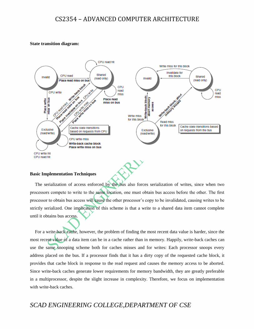
CS2354 – ADVANCED COMPUTER ARCHITECTURE
SCAD ENGINEERING COLLEGE,DEPARTMENT OF CSE
State transition diagram:
Basic Implementation Techniques
The serialization of access enforced by the bus also forces serialization of writes, since when two
processors compete to write to the same location, one must obtain bus access before the other. The first
processor to obtain bus access will cause the other processor‘s copy to be invalidated, causing writes to be
strictly serialized. One implication of this scheme is that a write to a shared data item cannot complete
until it obtains bus access.
For a write-back cache, however, the problem of finding the most recent data value is harder, since the
most recent value of a data item can be in a cache rather than in memory. Happily, write-back caches can
use the same snooping scheme both for caches misses and for writes: Each processor snoops every
address placed on the bus. If a processor finds that it has a dirty copy of the requested cache block, it
provides that cache block in response to the read request and causes the memory access to be aborted.
Since write-back caches generate lower requirements for memory bandwidth, they are greatly preferable
in a multiprocessor, despite the slight increase in complexity. Therefore, we focus on implementation
with write-back caches.

CS2354 – ADVANCED COMPUTER ARCHITECTURE
SCAD ENGINEERING COLLEGE,DEPARTMENT OF CSE
2. Explain the concept of distributed shared memory and also explain
directory based protocols with an example. (or) explain the numa
architecture with neat diagram.
There are several disadvantages in Symmetric Shared Memory architectures.
First, compiler mechanisms for transparent software cache coherence are very limited.
Second, without cache coherence, the multiprocessor loses the advantage of being able to fetch
and use multiple words in a single cache block for close to the cost of fetching one word.
Third, mechanisms for tolerating latency such as pre-fetch are more useful when they can
fetch multiple words, such as a cache block, and where the fetched data remain coherent; These
disadvantages are magnified by the large latency of access to remote memory versus a local
cache.
For these reasons, cache coherence is an accepted requirement in small-scale
multiprocessors. For larger-scale architectures, there are new challenges to extending the cache-
coherent shared-memory model. Although the bus can certainly be replaced with a more scalable
interconnection network and we could certainly distribute the memory so that the memory
bandwidth could also be scaled, the lack of scalability of the snooping coherence scheme needs to
be addressed is known as Distributed Shared Memory architecture.
The first coherence protocol is known as a directory protocol. A directory keeps the state of every
block that may be cached. Information in the directory includes which caches have copies of the
block, whether it is dirty, and so on.
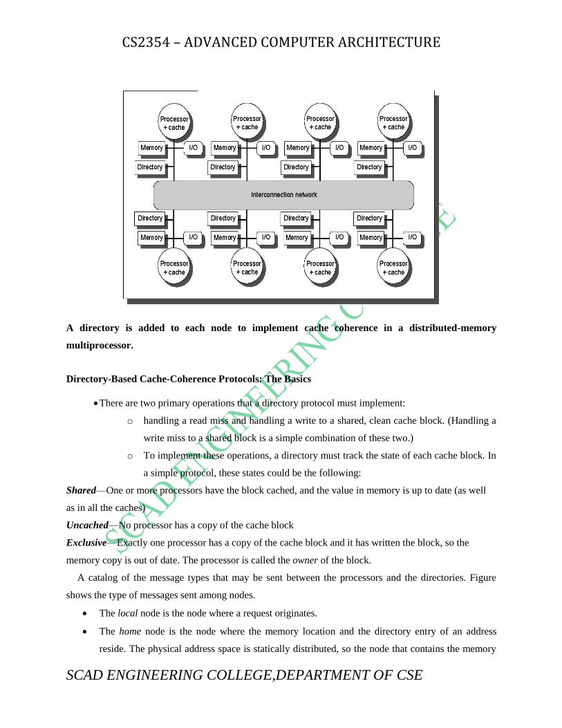
CS2354 – ADVANCED COMPUTER ARCHITECTURE
SCAD ENGINEERING COLLEGE,DEPARTMENT OF CSE
A directory is added to each node to implement cache coherence in a distributed-memory
multiprocessor.
Directory-Based Cache-Coherence Protocols: The Basics
There are two primary operations that a directory protocol must implement:
o handling a read miss and handling a write to a shared, clean cache block. (Handling a
write miss to a shared block is a simple combination of these two.)
o To implement these operations, a directory must track the state of each cache block. In
a simple protocol, these states could be the following:
Shared—One or more processors have the block cached, and the value in memory is up to date (as well
as in all the caches)
Uncached—No processor has a copy of the cache block
Exclusive—Exactly one processor has a copy of the cache block and it has written the block, so the
memory copy is out of date. The processor is called the owner of the block.
A catalog of the message types that may be sent between the processors and the directories. Figure
shows the type of messages sent among nodes.
The local node is the node where a request originates.
The home node is the node where the memory location and the directory entry of an address
reside. The physical address space is statically distributed, so the node that contains the memory

CS2354 – ADVANCED COMPUTER ARCHITECTURE
SCAD ENGINEERING COLLEGE,DEPARTMENT OF CSE
and directory for a given physical address is known. For example, the high-order bits may
provide the node number, while the low-order bits provide the offset within the memory on that
node. The local node may also be the home node. The directory must be accessed when the home
node is the local node, since copies may exist in yet a third node, called a remote node.
A remote node is the node that has a copy of a cache block, whether exclusive (in which case it is
the only copy) or shared. A remote node may be the same as either the local node or the home
node. In such cases, the basic protocol does not change, but interprocessor messages may be
replaced with intraprocessor messages.
Message
type Source Destination
Message
contents Function of this message
Read miss Local cache Home
directory
P, A Processor P has a read miss at
address A; request data and make P
a read sharer.
Write miss Local cache Home
directory
P, A Processor P has a write miss at
address A; — request data and make
P the exclusive owner.
Invalidate Home
directory
Remote
cache
A Invalidate a shared copy of data at
address A.
Fetch Home
directory
Remote
cache
A Fetch the block at address A and
send it to its home directory; change
the state of A in the remote cache to
shared.
Fetch/invali
date
Home
directory
Remote
cache
A Fetch the block at address A and
send it to its home directory;
invalidate the block in the cache.
Data value
reply
Home
directory
Local cache D Return a data value from the home
memory.
Data write
back
Remote
cache
Home
directory
A, D Write back a data value for address
A.
(where P=requesting processor number), A=requested address, and D=data contents).

CS2354 – ADVANCED COMPUTER ARCHITECTURE
SCAD ENGINEERING COLLEGE,DEPARTMENT OF CSE
Example :
State transition diagram for an individual cache block in a directory-based system.

CS2354 – ADVANCED COMPUTER ARCHITECTURE
SCAD ENGINEERING COLLEGE,DEPARTMENT OF CSE
To understand these directory operations, let‘s examine the requests received and actions taken
state by state. When a block is in the uncached state, the copy in memory is the current value, so
the only possible requests for that block are
_ Read miss—The requesting processor is sent the requested data from memory, and the
requestor is made the only sharing node. The state of the block is made shared.
_ Write miss—The requesting processor is sent the value and becomes the sharing node. The
block is made exclusive to indicate that the only valid copy is cached. Sharers indicate the
identity of the owner.
When the block is in the shared state, the memory value is up to date, so the same two requests
can occur:
_ Read miss—The requesting processor is sent the requested data from memory, and the
requesting processor is added to the sharing set.
_ Write miss—The requesting processor is sent the value. All processors in the set Sharers are
sent invalidate messages, and the Sharers set is to contain the identity of the requesting
processor. The state of the block is made exclusive.
When the block is in the exclusive state, the current value of the block is held in the cache of the
processor identified by the set Sharers (the owner), so there are three possible directory requests:
_ Read miss—The owner processor is sent a data fetch message, which causes the state of the
block in the owner‘s cache to transition to shared and causes the owner to send the data to the
directory, where it is written to memory and sent back to the requesting processor. The identity
of the requesting processor is added to the set Sharers, which still contains the identity of the
processor that was the owner (since it still has a readable copy).
_ Data write back—The owner processor is replacing the block and therefore must write it back.
This write back makes the memory copy up to date (the home directory essentially becomes the
owner), the block is now uncached, and the Sharers set is empty.
_ Write miss—The block has a new owner. A message is sent to the old owner, causing the cache
to invalidate the block and send the value to the directory, from which it is sent to the requesting
processor, which becomes the new owner. Sharers is set to the identity of the new owner, and the
state of the block remains exclusive.

CS2354 – ADVANCED COMPUTER ARCHITECTURE
SCAD ENGINEERING COLLEGE,DEPARTMENT OF CSE
3. Explain the basics of multithreading and it types. (8) (or) explain how
multihreading approach can be used to exploit thread level parallelism
within a processor? (8)
Multithreading allows multiple threads to share the functional units of a single processor in an
overlapping fashion. To permit this sharing, the processor must duplicate the independent state of each
thread. For example, a separate copy of the register file, a separate PC, and a separate page table are
required for each thread.
There are two main approaches to multithreading.
Fine-grained multithreading switches between threads on each instruction, causing the execution of
multiples threads to be interleaved. This interleaving is often done in a round-robin fashion, skipping any
threads that are stalled at that time.
Coarse-grained multithreading was invented as an alternative to fine-grained multithreading.
Coarse-grained multithreading switches threads only on costly stalls, such as level two cache misses. This
change relieves the need to have thread-switching be essentially free and is much less likely to slow the
processor down, since instructions from other threads will only be issued, when a thread encounters a
costly stall.
Simultaneous Multithreading: Converting Thread-Level Parallelism into Instruction-Level Parallelism:
Simultaneous multithreading (SMT) is a variation on multithreading that uses the resources of a multiple
issue, dynamically-scheduled processor to exploit TLP at the same time it exploits ILP. The key insight
that motivates SMT is that modern multiple-issue processors often have more functional unit parallelism
available than a single thread can effectively use. Furthermore, with register renaming and dynamic
scheduling, multiple instructions from independent threads can be issued without regard to the
dependences among them; the resolution of the dependences can be handled by the dynamic scheduling
capability.
Figure 6.44 conceptually illustrates the differences in a processor‘s ability to exploit the resources of a
superscalar for the following processor configurations:
n a superscalar with no multithreading support,

CS2354 – ADVANCED COMPUTER ARCHITECTURE
SCAD ENGINEERING COLLEGE,DEPARTMENT OF CSE
n a superscalar with coarse-grained multithreading,
n a superscalar with fine-grained multithreading, and
n a superscalar with simultaneous multithreading.
Issue Slots
Superscalar Coarse MT Fine MT SMT
In the superscalar without multithreading support, the use of issue slots is limited by a lack of ILP.
In the coarse-grained multithreaded superscalar, the long stalls are partially hidden by switching to
another thread that uses the resources of the processor.
In the fine-grained case, the interleaving of threads eliminates fully empty slots. Because only one thread
issues instructions in a given clock cycle.
In the SMT case, thread-level parallelism (TLP) and instruction-level parallelism (ILP) are exploited
simultaneously; with multiple threads using the issue slots in a single clock cycle.
Design Challenges in SMT processors
There are a variety of design challenges for an SMT processor, including:
Dealing with a larger register file needed to hold multiple contexts,

CS2354 – ADVANCED COMPUTER ARCHITECTURE
SCAD ENGINEERING COLLEGE,DEPARTMENT OF CSE
Maintaining low overhead on the clock cycle, particularly in critical steps such as instruction
issue, where more candidate instructions need to be considered, and in instruction completion,
where choosing what instructions to commit may be challenging, and
Ensuring that the cache conflicts generated by the simultaneous execution of multiple threads
do not cause significant performance degradation.
In viewing these problems, two observations are important. In many cases, the potential performance
overhead due to multithreading is small, and simple choices work well enough. Second, the efficiency of
current super-scalars is low enough that there is room for significant improvement, even at the cost of
some overhead.
4. Explain in detail about the need for consistency models and it types.(8)
Cache coherence ensures that multiple processors see a consistent view of
memory.
It does not answer the question of how consistent the view of memory must be. By ―how
consistent‖ we mean, when must a processor see a value that has been updated by another
processor? Since processors communicate through shared variables (used both for data
values and for synchronization), the question boils down to this: In what order must a
processor observe the data writes of another processor? Since the only way to ―observe
the writes of another processor‖ is through reads, the question becomes, What properties
must be enforced among reads and writes to different locations by different processors?
Although the question of how consistent memory must be seems simple, it is
remarkably complicated, as we can see with a simple example.
Here are two code segments from processes P1 and P2, shown side by side:
P1: A = 0; P2: B = 0;
..... .....
A = 1; B = 1;
L1: if (B == 0) ... L2: if (A == 0)...
Assume that the processes are running on different processors, and that locations A and B
are originally cached by both processors with the initial value of 0.
If writes always take immediate effect and are immediately seen by other processors, it
will be impossible for both if statements (labeled L1 and L2) to evaluate their conditions
as true, since reaching the if statement means that either A or B must have been assigned
the value 1. But suppose the write invalidate is delayed, and the processor is allowed to
continue during this delay; then it is possible that both P1 and P2 have not seen the
invalidations for B and A (respectively) before they attempt to read the values. The
question is, Should this behavior be allowed, and if so, under what conditions?

CS2354 – ADVANCED COMPUTER ARCHITECTURE
SCAD ENGINEERING COLLEGE,DEPARTMENT OF CSE
SEQUENTIAL CONSISTENCY:
The most straightforward model for memory consistency is called sequential consistency.
Sequential consistency requires that the result of any execution be the same as if the
memory accesses executed by each processor were kept in order and the accesses among
different processors were arbitrarily interleaved.
Sequential consistency eliminates the possibility of some nonobvious execution in the
previous example because the assignments must be completed before the if statements are
initiated.
The simplest way to implement sequential consistency is to require a processor to delay
the completion of any memory access until all the invalidations caused by that access are
completed. Of course, it is equally effective to delay the next memory access until the
previous one is completed. Remember that memory consistency involves operations
among different variables: the two accesses that must be ordered are actually to different
memory locations. In our example, we must delay the read of A or B (A == 0 or B == 0)
until the previous write has completed (B = 1 or A = 1). Under sequential consistency, we
cannot, for example, simply place the write in a write buffer and continue with the read.
Relaxed Consistency Models:
The key idea in relaxed consistency models is to allow reads and writes to complete
out of order, but to use synchronization operations to enforce ordering, so that a synchronized
program behaves as if the processor were sequentially consistent.
There are a variety of relaxed models that are classified according to what read and write
orderings they relax. We specify the orderings by a set of rules of the form X→Y, meaning that
operation X must complete before operation Y is done. Sequential consistency requires
maintaining all four possible orderings:
R→W,
R→R,
W→R,
and W→W.
The relaxed models are defined by which of these four sets of orderings they relax:
1. Relaxing the W→R ordering yields a model known as total store ordering or processor
consistency. Because this ordering retains ordering among writes, many programs that operate
under sequential consistency operate under this model, without additional synchronization.
2. Relaxing the W→W ordering yields a model known as partial store order.

CS2354 – ADVANCED COMPUTER ARCHITECTURE
SCAD ENGINEERING COLLEGE,DEPARTMENT OF CSE
3. Relaxing the R→W and R→R orderings yields a variety of models including weak ordering,
the PowerPC consistency model, and release consistency, depending on the details of the
ordering restrictions and how synchronization operations enforce ordering.
By relaxing these orderings, the processor can possibly obtain significant performance
advantages. There are, however, many complexities in describing relaxed consistency models,
including the advantages and complexities of relaxing different orders, defining precisely what it
means for a write to complete, and deciding when processors can see values that the processor
itself has written.
5. Explain the performance of the symmetric shared memory with
necessary graphs. (16)
Overall cache performance is a combination of
a. Uniprocessor cache miss traffic
b. Traffic caused by communication – invalidation and subsequent cache misses
Changing the processor count, cache size, and block size can affect these two components of miss
rate
Uniprocessor miss rate: compulsory, capacity, conflict
Communication miss rate: coherence misses
c. True sharing misses + false sharing misses
True sharing miss
d. The first write by a PE to a shared cache block causes an invalidation to establish
ownership of that block
e. When another PE attempts to read a modified word in that cache block, a miss occurs and
the resultant block is transferred
False sharing miss
f. Occur when a block a block is invalidate (and a subsequent reference causes a miss)
because some word in the block, other than the one being read, is written to
g. The block is shared, but no word in the cache is actually shared, and this miss would not
occur if the block size were a single word
True and False Sharing Miss Example

CS2354 – ADVANCED COMPUTER ARCHITECTURE
SCAD ENGINEERING COLLEGE,DEPARTMENT OF CSE
• Assume that words x1 and x2 are in the same cache block, which is in the shared state in the
caches of P1 and P2. Assuming the following sequence of events, identify each miss as a true
sharing miss or a false sharing miss.
Time P1 P2
1 Write x1
2 Read x2
3 Write x1
4 Write x2
5 Read x2
Example Result
1: True sharing miss (invalidate P2)
2: False sharing miss
– x2 was invalidated by the write of P1, but that value of x1 is not used in P2
3: False sharing miss
– The block containing x1 is marked shared due to the read in P2, but P2 did not read x1. A
write miss is required to obtain exclusive access to the block
4: False sharing miss
5: True sharing miss
Distribution of Execution Time in the Multi-programmed Parallel Make Workload
User
Execution
Kernel
Execution
Synchronization
Wait
CPU idle for I/O

CS2354 – ADVANCED COMPUTER ARCHITECTURE
SCAD ENGINEERING COLLEGE,DEPARTMENT OF CSE
% instruction
executed
27 3 1 69
% execution
time
27 7 2 64
A significant I-cache performance loss (at least for OS)
I-cache miss rate in OS for a 64-byte block size, 2-way se associative:
1.7% (32KB) – 0.2% (256KB)
I-cache miss rate in user-level: 1/6 of OS rate
Miss Rate VS. Block Size

CS2354 – ADVANCED COMPUTER ARCHITECTURE
SCAD ENGINEERING COLLEGE,DEPARTMENT OF CSE
Miss Rate VS. Block Size for Kernel
6.

CS2354 – ADVANCED COMPUTER ARCHITECTURE
SCAD ENGINEERING COLLEGE,DEPARTMENT OF CSE
6. Explain the classification of flynns taxonomy of multiprocessor
computers. (6)

CS2354 – ADVANCED COMPUTER ARCHITECTURE
SCAD ENGINEERING COLLEGE,DEPARTMENT OF CSE
I)Single instruction stream, single data stream (SISD)—
This category is the uniprocessor.
II) Single instruction stream, multiple data streams (SIMD)—
The same instruction is executed by multiple processors using different data streams.
SIMD computers exploit data-level parallelism by applying the same operations to
multiple items of data in parallel.
Each processor has its own data memory (hence multiple data), but there is a single
instruction memory and control processor, which fetches and dispatches instructions. For
applications that display significant data-level parallelism, the SIMD approach can be
very efficient.
III) Multiple instruction streams, single data stream (MISD)—No commercial
multiprocessor of this type has been built to date.
IV) Multiple instruction streams, multiple data streams (MIMD)—
Each processor fetches its own instructions and operates on its own data. MIMD
computers exploit thread-level parallelism , since multiple threads operate in parallel.
In general, thread-level parallelism is more flexible than data-level parallelism and
thus more generally applicable.

CS2354 – ADVANCED COMPUTER ARCHITECTURE
SCAD ENGINEERING COLLEGE,DEPARTMENT OF CSE
UNIT-III
PART-A
1. What are multiprocessors? Mention the categories of multiprocessors?
Multiprocessors are used to increase performance and improve availability. The different
categories are
SISD(Single Instruction and Single Data stream),
SIMD(Single Instruction and Multiple Data stream),
MISD(Multiple Instruction and Single data stream)
MIMD(Multiple Instruction and Multiple Data stream)
2. What are threads?
These are multiple processors executing a single program and sharing the code and most of their
address space. When multiple processors share code and data in the way, they are often called
threads.
3. What is cache coherence problem?
Two different processors have two different values for the same location.
4. What are the ways to maintain cache coherence? OR what are the ways to enforce cache
coherence?
Directory based protocol, Snooping based protocol.
5. What are the ways to maintain cache coherence using snooping protocol?
Write invalidate protocol, write update or write broadcast protocol.
6. What is write invalidate and write update protocol?
Write invalidate provide exclusive access to caches. These exclusive caches ensure that
no other readable or writable copies of an item exist when the write occurs.
Write updates protocol updates all cached copies of a data item when that item is written.
7. What are the disadvantages of using symmetric shared memor?
Compiler mechanisms are very limited, and create large latency for remote memory access
fetching multiple words in a single cache block will increase the cost.
8. Mention the information available in the directory?
The directory keeps the state of each block that is cached. It keeps track of which caches have
copies of the block.
9. What are the states of cache block in directory based approach?
Shared, Un-cached and Exclusive.
10. What are the uses of having a bit vector?
When a block is shared, the bit vector indicates whether the processor has the copy of the block.
When block is in exclusive state, bit vector keep track of the owner of the block.
11. When do we say that a cache block is exclusive?

CS2354 – ADVANCED COMPUTER ARCHITECTURE
SCAD ENGINEERING COLLEGE,DEPARTMENT OF CSE
When exactly one processor has the copy of the cache block, and it has written the block, then the
processor is called the owner of the block. During this phase the block will be in exclusive state.
12. Explain the types of messages that can be send between the processors and directories?
Local Node: node where the requests originates
Home Node: Node where memory location and directory entry of the address resides.
Remote Note: the copy of the block in the third node called remote node.
13. What is consistency? And what are the models used for consistency?
Consistency says in what order processor must observe the data writes of another processor.
Models used for Consistency:
Sequential Consistency Model,
Relaxed Consistency Model
14. What is sequential consistency?
Sequential consistency requires that the result of any execution be the same, as if the memory
accesses executed by each processor were kept in order and the accesses among different
processors were interleaved.
15. What is relaxed consistency model?
Relaxed consistency model allows reads and writes to be executed out of order.
Three sets of ordering are:
W->R Ordering – Total store ordering
W->W Ordering – Partial ordering
R->W and R->R Ordering – Weak ordering
16. What is coarse grained and fine grained multithreading?
Coarse Grained: it switches only on costly stalls (or) event. Thus it is much less likely to slow
down the execution of an individual thread.
Fine Grained: it switches threads between threads on each instruction, causing the execution of
multiple threads to be interleaved.

CS2354 – ADVANCED COMPUTER ARCHITECTURE
SCAD ENGINEERING COLLEGE,DEPARTMENT OF CSE
UNIT IV
MEMORY AND I/O
Cache performance – Reducing cache miss penalty and miss rate – Reducing hit time – Main memory and performance – Memory technology. Types of storage devices – Buses – RAID – Reliability, availability and dependability – I/O performance measures – Designing an I/O system.
1. Explain in detail about the vaious optimization techniques for
improving the cache performance. (16)
Cache performance
The average memory access time is calculated as follows
Average memory access time = hit time + Miss rate x Miss Penalty.
Where Hit Time is the time to deliver a block in the cache to the processor (includes time to determine
whether the block is in the cache), Miss Rate is the fraction of memory references not found in cache
(misses/references) and Miss Penalty is the additional time required because of a miss.
The average memory access time due to cache misses predicts processor performance.
First, there are other reasons for stalls, such as contention due to I/O devices using memory and
due to cache misses.
Second, The CPU stalls during misses, and the memory stall time is strongly correlated to
average memory access time.
CPU time = (CPU execution clock cycles + Memory stall clock cycles) × Clock cycle time
There are 17 cache optimizations into four categories:
1 Reducing the miss penalty: multilevel caches, critical word first, read miss before write miss,
merging write buffers, victim caches;
2 Reducing the miss rate: larger block size, larger cache size, higher associativity, pseudo-
associativity, and compiler optimizations;
3 Reducing the miss penalty or miss rate via parallelism: nonblocking caches, hardware
prefetching, and compiler prefetching;

CS2354 – ADVANCED COMPUTER ARCHITECTURE
SCAD ENGINEERING COLLEGE,DEPARTMENT OF CSE
4 Reducing the time to hit in the cache: small and simple caches, avoiding address translation, and
pipelined cache access.
There are five optimizations techniques to reduce miss penalty.
i) First Miss Penalty Reduction Technique: Multi-Level Caches
The First Miss Penalty Reduction Technique follows the Adding another level of cache between
the original cache and memory. The first-level cache can be small enough to match the clock cycle time
of the fast CPU and the second-level cache can be large enough to capture many accesses that would go
to main memory, thereby the effective miss penalty.
The definition of average memory access time for a two-level cache. Using the subscripts L1 and
L2 to refer, respectively, to a first-level and a second-level cache, the formula is
Average memory access time = Hit timeL1
+ Miss rateL1
× Miss penaltyL1
and Miss penaltyL1
= Hit timeL2
+ Miss rateL2
× Miss penaltyL2
so Average memory access time = Hit timeL1
+ Miss rateL1
× (Hit timeL2
+ Miss rateL2
× Miss penaltyL2
)
Local miss rate—This rate is simply the number of misses in a cache divided by the total number of
memory accesses to this cache. As you would expect, for the first-level cache it is equal to Miss rateL1
and
for the second-level cache it is Miss rateL2
.
Global miss rate—The number of misses in the cache divided by the total num-ber of memory accesses
generated by the CPU. Using the terms above, the global miss rate for the first-level cache is still just
Miss rateL1
but for the second-level cache it is Miss rateL1
× Miss rateL2
.
Memory
disk L1 cache Regs
L2 cache
Processor

CS2354 – ADVANCED COMPUTER ARCHITECTURE
SCAD ENGINEERING COLLEGE,DEPARTMENT OF CSE
Average memory stalls per instruction = Misses per instructionL1
× Hit timeL2
+ Misses per instructionL2
×
Miss penaltyL2
.
we can consider the parameters of second-level caches. The foremost difference between the two levels
is that the speed of the first-level cache affects the clock rate of the CPU, while the speed of the second-
level cache only affects the miss penalty of the first-level cache.
Figures show how miss rates and relative execution time change with the size of a second-level cache
for one design.
ii) Second Miss Penalty Reduction Technique: Critical Word First and Early Restart
Multilevel caches require extra hardware to reduce miss penalty, but not this second technique. It
is based on the observation that the CPU normally needs just one word of the block at a time. This
strategy is impatience: Don‘t wait for the full block to be loaded before sending the requested word and
restarting the CPU. Here are two specific strategies:
Critical word first—Request the missed word first from memory and send it to the CPU as soon as it
arrives; let the CPU continue execution while filling the rest of the words in the block. Critical-word-first
fetch is also called wrapped fetch and requested word first.
Early restart—Fetch the words in normal order, but as soon as the requested word of the block arrives,
send it to the CPU and let the CPU continue execution.
iii) Third Miss Penalty Reduction Technique: Giving Priority to Read Misses over Writes
This optimization serves reads before writes have been completed. We start with looking at complexities
of a write buffer. With a write-through cache the most important improvement is a write buffer of the

CS2354 – ADVANCED COMPUTER ARCHITECTURE
SCAD ENGINEERING COLLEGE,DEPARTMENT OF CSE
proper size. Write buffers, however, do complicate memory accesses in that they might hold the updated
value of a location needed on a read miss. The simplest way out of this is for the read miss to wait until
the write buffer is empty. The alternative is to check the contents of the write buffer on a read miss, and if
there are no conflicts and the memory system is available, let the read miss continue.
iv) Fourth Miss Penalty Reduction Technique: Merging Write Buffer
This technique also involves write buffers, this time improving their efficiency. Write through caches rely
on write buffers, as all stores must be sent to the next lower level of the hierarchy. As mentioned above,
even write back caches use a simple buffer when a block is replaced. If the write buffer is empty, the data
and the full address are written in the buffer, and the write is finished from the CPU's perspective; the
CPU continues working while the write buffer prepares to write the word to memory. If the buffer
contains other modified blocks, the addresses can be checked to see if the address of this new data
matches the address of the valid write buffer entry. If so, the new data are combined with that entry,
called write merging.
If the buffer is full and there is no address match, the cache (and CPU) must wait until the buffer has an
empty entry. This optimization uses the memory more efficiently since multiword writes are usually
faster than writes performed one word at a time.

CS2354 – ADVANCED COMPUTER ARCHITECTURE
SCAD ENGINEERING COLLEGE,DEPARTMENT OF CSE
The optimization also reduces stalls due to the write buffer being full. Figure shows a write buffer
with and without write merging. Assume we had four entries in the write buffer, and each entry could
hold four 64-bit words. Without this optimization, four stores to sequential addresses would fill the buffer
at one word per entry, even though these four words when merged exactly fit within a single entry of the
write buffer. The four writes are merged into a single buffer entry with write merging; without it, the
buffer is full even though three-fourths of each entry is wasted. The buffer has four entries, and each entry
holds four 64-bit words. The address for each entry is on the left, with valid bits (V) indicating whether or
not the next sequential eight bytes are occupied in this entry. (Without write merging, the words to the
right in the upper drawing would only be used for instructions which wrote multiple words at the same
time.)
v) Fifth Miss Penalty Reduction Technique: Victim Caches
One approach to lower miss penalty is to remember what was discarded in case it is needed again. Since
the discarded data has already been fetched, it can be used again at small cost.
Such ―recycling‖ requires a small, fully associative cache between a cache and its refill path. Figure
5.13 shows the organization. This victim cache contains only blocks that are discarded from a cache
because of a miss ―victims‖ and are checked on a miss to see if they have the desired data before going to
the next lower-level memory. If it is found there, the victim block and cache block are swapped. The
AMD Athlon has a victim cache with eight entries.

CS2354 – ADVANCED COMPUTER ARCHITECTURE
SCAD ENGINEERING COLLEGE,DEPARTMENT OF CSE
Reducing cache miss penalty and miss rate
The classical approach to improving cache behavior is to reduce miss rates, and there are five techniques
to reduce miss rate. we first start with a model that sorts all misses into three simple categories:
Compulsory—The very first access to a block cannot be in the cache, so the block must be brought into
the cache. These are also called cold start misses or first reference misses.
Capacity—If the cache cannot contain all the blocks needed during execution of a program, capacity
misses (in addition to compulsory misses) will occur be-cause of blocks being discarded and later
retrieved.
Conflict—If the block placement strategy is set associative or direct mapped, conflict misses (in addition
to compulsory and capacity misses) will occur be-cause a block may be discarded and later retrieved if
too many blocks map to its set. These misses are also called collision misses or interference misses. The
idea is that hits in a fully associative cache which become misses in an N-way set associative cache are
due to more than N requests on some popular sets.
i ) First Miss Rate Reduction Technique: Larger Block Size
The simplest way to reduce miss rate is to increase the block size. Figure shows the trade-off of block size
versus miss rate for a set of programs and cache sizes. Larger block sizes will reduce compulsory misses.
This reduction occurs because the principle of locality has two components: temporal locality and spatial

CS2354 – ADVANCED COMPUTER ARCHITECTURE
SCAD ENGINEERING COLLEGE,DEPARTMENT OF CSE
locality. Larger blocks take advantage of spatial locality.
Miss rate versus block size for five different-sized caches.
At the same time, larger blocks increase the miss penalty. Since they reduce the number of blocks in
the cache, larger blocks may increase conflict misses and even capacity misses if the cache is small.
Clearly, there is little reason to increase the block size to such a size that it increases the miss rate. There
is also no benefit to reducing miss rate if it increases the average memory access time. The increase in
miss penalty may outweigh the decrease in miss rate.
ii) Second Miss Rate Reduction Technique: Larger caches
The obvious way to reduce capacity misses in the above is to increases capacity of the cache. The obvious
drawback is longer hit time and higher cost. This technique has been especially popular in off-chip
caches: The size of second or third level caches in 2001 equals the size of main memory in desktop
computers.
iii) Third Miss Rate Reduction Technique: Higher Associativity:
Generally the miss rate improves with higher associativity. There are two general rules of thumb that can
be drawn. The first is that eight-way set associative is for practical purposes as effective in reducing
misses for these sized caches as fully associative. You can see the difference by comparing the 8-way

CS2354 – ADVANCED COMPUTER ARCHITECTURE
SCAD ENGINEERING COLLEGE,DEPARTMENT OF CSE
entries to the capacity miss, since capacity misses are calculated using fully associative cache.
iv) Fourth Miss Rate Reduction Technique: Way Prediction and Pseudo-Associative Caches
In way-prediction, extra bits are kept in the cache to predict the set of the next cache access. This
prediction means the multiplexer is set early to select the desired set, and only a single tag comparison is
performed that clock cycle. A miss results in checking the other sets for matches in subsequent clock
cycles.
The Alpha 21264 uses way prediction in its instruction cache. (Added to each block of the instruction
cache is a set predictor bit. The bit is used to select which of the two sets to try on the next cache access.
If the predictor is correct, the instruction cache latency is one clock cycle. If not, it tries the other set,
changes the set predictor, and has a latency of three clock cycles.
v) Fifth Miss Rate Reduction Technique: Compiler Optimizations
Code can easily be rearranged without affecting correctness; for example, reordering the procedures of
a program might reduce instruction miss rates by reducing conflict misses. Reordering the instructions
reduced misses by 50% for a 2-KB direct-mapped instruction cache with 4-byte blocks, and by 75% in an
8-KB cache.
Another code optimization aims for better efficiency from long cache blocks. Aligning basic blocks so
that the entry point is at the beginning of a cache block decreases the chance of a cache miss for
sequential code.
Loop Interchange:
Some programs have nested loops that access data in memory in non-sequential order. Simply
exchanging the nesting of the loops can make the code access the data in the order it is stored. Assuming
the arrays do not fit in cache, this technique reduces misses by improving spatial locality; reordering
maximizes use of data in a cache block before it is discarded.
/* Before */
for (j = 0; j < 100; j = j+1)
for (i = 0; i < 5000; i = i+1)
x[i][j] = 2 * x[i][j];
/* After */

CS2354 – ADVANCED COMPUTER ARCHITECTURE
SCAD ENGINEERING COLLEGE,DEPARTMENT OF CSE
for (i = 0; i < 5000; i = i+1)
for (j = 0; j < 100; j = j+1)
x[i][j] = 2 * x[i][j];
This optimization improves cache performance without affecting the number of instructions executed.
2. What is virtual memory? Write techniques for fast address translation
Virtual memory divides physical memory into blocks (called page or segment) and allocates them to
different processes. With virtual memory, the CPU produces virtual addresses that are translated by a
combination of HW and SW to physical addresses, which accesses main memory. The process is called
memory mapping or address translation. Today, the two memory-hierarchy levels controlled by virtual
memory are DRAMs and magnetic disks
Virtual Memory manages the two levels of the memory hierarchy represented by main memory and
secondary storage. Figure 5.31 shows the mapping of virtual memory to physical memory for a program
with four pages.
There are further differences between caches and virtual memory beyond those quantitative ones
mentioned in Figure 5.32

CS2354 – ADVANCED COMPUTER ARCHITECTURE
SCAD ENGINEERING COLLEGE,DEPARTMENT OF CSE
:
Virtual memory also encompasses several related techniques. Virtual memory systems can be
categorized into two classes: those with fixed-size blocks, called pages, and those with variable-size
locks, called segments. Pages are typically fixed at 4096 to 65,536 bytes, while segment size varies. The
largest segment supported on any processor ranges from 216
bytes up to 232
bytes; the smallest segment is
1 byte. Figure 5.33 shows how the two approaches might divide code and data.
The block can be placed anywhere in main memory. Both paging and segmentation rely on a data
structure that is indexed by the page or segment number. This data structure contains the physical address
of the block. For segmentation, the offset is added to the segment‘s physical address to obtain the final
physical address. For paging, the offset is simply concatenated to this physical page address (see Figure
5.35).

CS2354 – ADVANCED COMPUTER ARCHITECTURE
SCAD ENGINEERING COLLEGE,DEPARTMENT OF CSE
This data structure, containing the physical page addresses, usually takes the form of a page table.
Indexed by the virtual page number, the size of the table is the number of pages in the virtual address
space. Given a 32-bit virtual address, 4-KB pages, and 4 bytes per page table entry, the size of the page
table would be (232
/212
) × 22
= 222
or 4 MB.
To reduce address translation time, computers use a cache dedicated to these address translations,
called a translation look-aside buffer, or simply translation buffer. They are described in more detail
shortly.
With the help of Operating System and LRU algorithm pages can be replaced whenever page fault
occurs.
Techniques for Fast Address Translation
Page tables are usually so large that they are stored in main memory, and some-times paged themselves.
Paging means that every memory access logically takes at least twice as long, with one memory access to
obtain the physical address and a second access to get the data. This cost is far too dear.
One remedy is to remember the last translation, so that the mapping process is skipped if the current
address refers to the same page as the last one. A more general solution is to again rely on the principle of
locality; if the accesses have locality, then the address translations for the accesses must also have
locality. By keeping these address translations in a special cache, a memory access rarely re-quires a
second access to translate the data. This special address translation cache is referred to as a translation
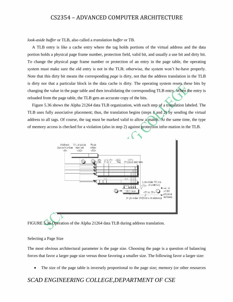
CS2354 – ADVANCED COMPUTER ARCHITECTURE
SCAD ENGINEERING COLLEGE,DEPARTMENT OF CSE
look-aside buffer or TLB, also called a translation buffer or TB.
A TLB entry is like a cache entry where the tag holds portions of the virtual address and the data
portion holds a physical page frame number, protection field, valid bit, and usually a use bit and dirty bit.
To change the physical page frame number or protection of an entry in the page table, the operating
system must make sure the old entry is not in the TLB; otherwise, the system won‘t be-have properly.
Note that this dirty bit means the corresponding page is dirty, not that the address translation in the TLB
is dirty nor that a particular block in the data cache is dirty. The operating system resets these bits by
changing the value in the page table and then invalidating the corresponding TLB entry. When the entry is
reloaded from the page table, the TLB gets an accurate copy of the bits.
Figure 5.36 shows the Alpha 21264 data TLB organization, with each step of a translation labeled. The
TLB uses fully associative placement; thus, the translation begins (steps 1 and 2) by sending the virtual
address to all tags. Of course, the tag must be marked valid to allow a match. At the same time, the type
of memory access is checked for a violation (also in step 2) against protection infor-mation in the TLB.
FIGURE 5.36 Operation of the Alpha 21264 data TLB during address translation.
Selecting a Page Size
The most obvious architectural parameter is the page size. Choosing the page is a question of balancing
forces that favor a larger page size versus those favoring a smaller size. The following favor a larger size:
The size of the page table is inversely proportional to the page size; memory (or other resources

CS2354 – ADVANCED COMPUTER ARCHITECTURE
SCAD ENGINEERING COLLEGE,DEPARTMENT OF CSE
used for the memory map) can therefore be saved by making the pages bigger.
A larger page size can allow larger caches with fast cache hit times.
Transferring larger pages to or from secondary storage, possibly over a network, is more efficient
than transferring smaller pages.
The number of TLB entries are restricted, so a larger page size means that more memory can be
mapped efficiently, thereby reducing the number of TLB misses.
3. Explain various types of storage devices (16)
Types of Storage Devices
There are various types of Storage devices such as magnetic disks, magnetic tapes, automated
tape libraries, CDs, and DVDs.
The First Storage device magnetic disks have dominated nonvolatile storage since 1965.
Magnetic disks play two roles in computer systems:
Long Term, nonvolatile storage for files, even when no programs are running
A level of the memory hierarchy below main memory used as a backing store for virtual memory
during program execution.

CS2354 – ADVANCED COMPUTER ARCHITECTURE
SCAD ENGINEERING COLLEGE,DEPARTMENT OF CSE
A magnetic disk consists of a collection of platters (generally 1 to 12), rotating on a spindle at 3,600
to 15,000 revolutions per minute (RPM). These platters are metal or glass disks covered with magnetic
recording material on both sides, so 10 platters have 20 recording surfaces.
The disk surface is divided into concentric circles, designated tracks. There are typically 5,000 to
30,000 tracks on each surface. Each track in turn is divided into sectors that contain the information; a
track might have 100 to 500 sectors. A sector is the smallest unit that can be read or written. IBM
mainframes allow users to select the size of the sectors, although most systems fix their size, typically at
512 bytes of data. The sequence recorded on the magnetic media is a sector number, a gap, the
information for that sector including error correction code, a gap, the sector number of the next sector,
and so on.
To read and write information into a sector, a movable arm containing a read/ write head is
located over each surface. To read or write a sector, the disk controller sends a command to move the arm
over the proper track. This operation is called a seek, and the time to move the arm to the desired track is
called seek time.

CS2354 – ADVANCED COMPUTER ARCHITECTURE
SCAD ENGINEERING COLLEGE,DEPARTMENT OF CSE
The time for the requested sector to rotate under the head is the rotation latency or rotational
delay. The average latency to the desired information is obviously halfway around the disk; if a disk
rotates at 10,000 revolutions per minute (RPM), the average rotation time is therefore
Average Rotation Time = 0.5/10,000RPM = 0.5/(10,000/60)RPM = 3.0ms
The next component of disk access, transfer time, is the time it takes to transfer a block of bits,
typically a sector, under the read-write head. This time is a function of the block size, disk size, rotation
speed, recording density of the track, and speed of the electronics connecting the disk to computer.
Transfer rates in 2001 range from 3 MB per second for the 3600 RPM, 1-inch drives to 65 MB per second
for the 15000 RPM, 3.5-inch drives.
The Future of Magnetic Disks
The disk industry has concentrated on improving the capacity of disks. Improvement in capacity is
customarily expressed as improvement in areal density, measured in bits per square inch:
Areal Density = (Tracks/Inch) on a disk surface X (Bits/Inch) on a track
Optical Disks:
One challenger to magnetic disks is optical compact disks, or CDs, and its successor, called
Digital Video Discs and then Digital Versatile Discs or just DVDs. Both the CD-ROM and DVD-ROM are
removable and inexpensive to manufacture, but they are read-only mediums. These 4.7-inch diameter
disks hold 0.65 and 4.7 GB, respectively, although some DVDs write on both sides to double their
capacity. Their high capacity and low cost have led to CD-ROMs and DVD-ROMs replacing floppy disks
as the favorite medium for distributing software and other types of computer data.
The popularity of CDs and music that can be downloaded from the WWW led to a market for
rewritable CDs, conveniently called CD-RW, and write once CDs, called CD-R. In 2001, there is a small
cost premium for drives that can record on CD-RW. The media itself costs about $0.20 per CD-R disk or
$0.60 per CD-RW disk. CD-RWs and CD-Rs read at about half the speed of CD-ROMs and CD-RWs and
CD-Rs write at about a quarter the speed of CD-ROMs.
Magnetic Tape:

CS2354 – ADVANCED COMPUTER ARCHITECTURE
SCAD ENGINEERING COLLEGE,DEPARTMENT OF CSE
Magnetic tapes have been part of computer systems as long as disks because they use the similar
technology as disks, and hence historically have followed the same density improvements. The inherent
cost/performance difference between disks and tapes is based on their geometries:
Fixed rotating platters offer random access in milliseconds, but disks have a limited storage area
and the storage medium is sealed within each reader.
Long strips wound on removable spools of ―unlimited‖ length mean many tapes can be used per
reader, but tapes require sequential access that can take seconds.
One of the limits of tapes had been the speed at which the tapes can spin without breaking or jamming.
A technology called helical scan tapes solves this problem by keeping the tape speed the same but
recording the information on a diagonal to the tape with a tape reader that spins much faster than the tape
is moving. This technology increases recording density by about a factor of 20 to 50. Helical scan tapes
were developed for low-cost VCRs and camcorders, which brought down the cost of the tapes and
readers.
Automated Tape Libraries
Tape capacities are enhanced by inexpensive robots to automatically load and store tapes,
offering a new level of storage hierarchy. These nearline tapes mean access to terabytes of information in
tens of seconds, without the intervention of a human operator.
Flash Memory
Embedded devices also need nonvolatile storage, but premiums placed on space and power
normally lead to the use of Flash memory instead of magnetic recording. Flash memory is also used as a
rewritable ROM in embedded systems, typically to allow software to be upgraded without having to
replace chips. Applications are typically prohibited from writing to Flash memory in such circumstances.
Like electrically erasable and programmable read-only memories (EEPROM), Flash memory is
written by inducing the tunneling of charge from transistor gain to a floating gate. The floating gate acts
as a potential well which stores the charge, and the charge cannot move from there without applying an
external force. The primary difference between EEPROM and Flash memory is that Flash restricts write
to multi-kilobyte blocks, increasing memory capacity per chip by reducing area dedicated to control.
Compared to disks, Flash memories offer low power consumption (less than 50 milliwatts), can be sold in
small sizes, and offer read access times comparable to DRAMs. In 2001, a 16 Mbit Flash memory has a
65 ns access time, and a 128 Mbit Flash memory has a 150 ns access time.

CS2354 – ADVANCED COMPUTER ARCHITECTURE
SCAD ENGINEERING COLLEGE,DEPARTMENT OF CSE
4. Explain the buses and I/O devices (16)
Buses were traditionally classified as CPU-memory buses or I/O buses. I/O buses may be lengthy,
may have many types of devices connected to them, have a wide range in the data bandwidth of the
devices connected to them, and normally follow a bus standard. CPU-memory buses, on the other hand,
are short, generally high speed, and matched to the memory system to maximize memory-CPU
bandwidth. During the design phase, the designer of a CPU-memory bus knows all the types of devices
that must connect together, while the I/O bus designer must accept devices varying in latency and
bandwidth capabilities. To lower costs, some computers have a single bus for both memory and I/O
devices. In the quest for higher I/O performance, some buses are a hybrid of the two. For example, PCI is
relatively short, and is used to connect to more traditional I/O buses via bridges that speak both PCI on
one end and the I/O bus protocol on the other. To indicate its intermediate state, such buses are sometimes
called mezzanine
Bus Design Decisions
The design of a bus presents several options, as Figure 7.8 shows. Like the rest of the computer
system, decisions depend on cost and performance goals. The first three options in the figure are clear—
separate address and data lines, wider data lines, and multiple-word transfers all give higher performance
at more cost.
Option High performance Low cost
Bus width Separate address and data lines Multiplex address and data lines
Data width Wider is faster (e.g., 64 bits) Narrower is cheaper (e.g., 8 bits)
Transfer size Multiple words have less bus overhead Single-word transfer is simpler
Bus masters Multiple (requires arbitration) Single master (no arbitration)
Split transaction?
Yes—separate request and reply
packets get higher bandwidth (need
multiple masters)
No—continuous connection is
cheaper and has lower latency
Clocking Synchronous Asynchronous
The next item in the table concerns the number of bus masters. These devices can initiate a read
or write transaction; the CPU, for instance, is always a bus master. A bus has multiple masters when there
are multiple CPUs or when I/O devices can initiate a bus transaction. With multiple masters, a bus can
offer higher bandwidth by using packets, as opposed to holding the bus for the full transaction. This
technique is called split transactions.

CS2354 – ADVANCED COMPUTER ARCHITECTURE
SCAD ENGINEERING COLLEGE,DEPARTMENT OF CSE
The final item in Figure 7.8, clocking, concerns whether a bus is synchronous or asynchronous. If
a bus is synchronous, it includes a clock in the control lines and a fixed protocol for sending address and
data relative to the clock. Since little or no logic is needed to decide what to do next, these buses can be
both fast and inexpensive.
Bus Standards
Standards that let the computer designer and I/O-device designer work independently play a large role
in buses. As long as both designers meet the requirements, any I/O device can connect to any computer.
The I/O bus standard is the document that defines how to connect devices to computers.
• The Good
– Let the computer and I/O-device designers work independently
– Provides a path for second party (e.g. cheaper) competition
• The Bad
– Become major performance anchors
– Inhibit change
• How to create a standard
– Bottom-up
• Company tries to get standards committee to approve it‘s latest philosophy in
hopes that they‘ll get the jump on the others (e.g. S bus, PC-AT bus, ...)
• De facto standards
– Top-down
• Design by committee (PCI, SCSI, ...)
Some sample bus designs are shown below

CS2354 – ADVANCED COMPUTER ARCHITECTURE
SCAD ENGINEERING COLLEGE,DEPARTMENT OF CSE
Interfacing Storage Devices to the CPU
The I/O bus is connected to the main memory bus is shown in figure 7.15

CS2354 – ADVANCED COMPUTER ARCHITECTURE
SCAD ENGINEERING COLLEGE,DEPARTMENT OF CSE
Processor interface with i/o bus can be done with two techniques one using interrupts and second
using memory mapped I/O
• I/O Control Structures
– Polling
– Interrupts
– DMA
– I/O Controllers
– I/O Processors
The simple interface, in which the CPU periodically checks status bits to see if it is time for the next
I/O operation, is called polling.
Interrupt-driven I/O, used by most systems for at least some devices, allows the CPU to work on some
other process while waiting for the I/O device. For example, the LP11 has a mode that allows it to
interrupt the CPU whenever the done bit or error bit is set. In general-purpose applications, interrupt-
driven I/O is the key to multitasking operating systems and good response times.
The drawback to interrupts is the operating system overhead on each event. In real-time
applications with hundreds of I/O events per second, this overhead can be intolerable. One hybrid solution
for real-time systems is to use a clock to periodically interrupt the CPU, at which time the CPU polls all
I/O devices
The DMA hardware is a specialized processor that transfers data between memory and an I/O
device while the CPU goes on with other tasks. Thus, it is external to the CPU and must act as a master
on the bus. The CPU first sets up the DMA registers, which contain a memory address and number of
bytes to be transferred. More sophisticated DMA devices support scatter/gather, whereby a DMA device
can write or read data from a list of separate addresses. Once the DMA transfer is complete, the DMA
controller interrupts the CPU. There may be multiple DMA devices in a computer system.
5. Briefly explain RAID (or) Redundant arrays of inexpensive disks (8)
An innovation that improves both dependability and performance of storage systems is disk
arrays. One argument for arrays is that potential throughput can be increased by having many disk drives
and, hence, many disk arms, rather than one large drive with one disk arm. Although a disk array would
have more faults than a smaller number of larger disks when each disk has the same reliability,

CS2354 – ADVANCED COMPUTER ARCHITECTURE
SCAD ENGINEERING COLLEGE,DEPARTMENT OF CSE
dependability can be improved by adding redundant disks to the array to tolerate faults. That is, if a single
disk fails, the lost information can be reconstructed from redundant information. The only danger is in
having another disk fail between the time the first disk fails and the time it is replaced (termed mean time
to repair, or MTTR). Since the mean time to failure (MTTF) of disks is tens of years, and the MTTR is
measured in hours, redundancy can make the measured reliability of 100 disks much higher than that of a
single disk. These systems have become known by the acronym RAID, stand-ing originally for redundant
array of inexpensive disks, although some have re-named it to redundant array of independent disks
RAID level Minimum
number of
Disk
faults
survived
Example
Data
disks
Corresponding
Check disks
Corporations producing
RAID products at this level
0 Non-redundant
striped 0 8 0 Widely used
1 Mirrored 1 8 8 EMC, Compaq (Tandem),
IBM
2 Memory-style ECC 1 8 4
3 Bit-interleaved parity 1 8 1 Storage Concepts
4 Block-interleaved
parity 1 8 1 Network Appliance
5 Block-interleaved
distributed parity
1 8 1 Widely used
6 P+Q redundancy 2 8 2
FIGURE 7.17 RAID levels, their fault tolerance, and their overhead in redundant disks.
No Redundancy (RAID 0)
This notation is refers to a disk array in which data is striped but there is no redundancy to
tolerate disk failure. Striping across a set of disks makes the collection appear to software as a single large
disk, which simplifies storage management. It also improves performance for large accesses, since many
disks can operate at once. Video editing systems, for example, often stripe their data.
Mirroring (RAID 1)
This traditional scheme for tolerating disk failure, called mirroring or shadowing, uses twice as
many disks as does RAID 0. Whenever data is written to one disk, that data is also written to a redundant
disk, so that there are always two copies of the information. If a disk fails, the system just goes to the
―mirror‖ to get the desired information. Mirroring is the most expensive RAID solution, since it requires

CS2354 – ADVANCED COMPUTER ARCHITECTURE
SCAD ENGINEERING COLLEGE,DEPARTMENT OF CSE
the most disks.
Bit-Interleaved Parity (RAID 3)
The cost of higher availability can be reduced to 1/N, where N is the number of disks in a
protection group. Rather than have a complete copy of the original data for each disk, we need only add
enough redundant information to restore the lost information on a failure. Reads or writes go to all disks
in the group, with one extra disk to hold the check information in case there is a failure.
Parity is one such scheme. Readers unfamiliar with parity can think of the redundant disk as having the
sum of all the data in the other disks. When a disk fails, then you subtract all the data in the good disks
from the parity disk; the remaining information must be the missing information.
Block-Interleaved Parity and Distributed Block-Interleaved Parity (RAID 4 and RAID 5)
In RAID 3, every access went to all disks. Some applications would prefer to do smaller accesses,
allowing independent accesses to occur in parallel. That is the purpose of the next RAID levels. Since
error-detection information in each sector is checked on reads to see if data is correct, such ―small reads‖
to each disk can occur independently as long as the minimum access is one sector.
RAID 4 efficiently supports a mixture of large reads, large writes, small reads, and small writes. One
drawback to the system is that the parity disk must be updated on every write, so it is the bottleneck for
back-to-back writes. To fix the parity-write bottleneck, the parity information can be spread throughout
all the disks so that there is no single bottleneck for writes. The distributed parity organization is RAID 5.

CS2354 – ADVANCED COMPUTER ARCHITECTURE
SCAD ENGINEERING COLLEGE,DEPARTMENT OF CSE
Figure 7.19 shows how data are distributed in RAID 4 vs. RAID 5. As the organization on the right
shows, in RAID 5 the parity associated with each row of data blocks is no longer restricted to a single
disk. This organization allows multiple writes to occur simultaneously as long as the stripe units are not
located in the same disks. For example, a write to block 8 on the right must also access its parity block
P2, thereby occupying the first and third disks. A second write to block 5 on the right, implying an update
to its parity block P1, accesses the second and fourth disks and thus could occur at the same time as the
write to block 8. Those same writes to the organization on the left would result in changes to blocks P1
D0 D1 D2 D3 P D0'
+
+
D0
'
D1 D2 D
3
P'
new
data
old
data
old
parity
XOR
XO
(1. Read) (2. Read)
(3. Write) (4. Write)

CS2354 – ADVANCED COMPUTER ARCHITECTURE
SCAD ENGINEERING COLLEGE,DEPARTMENT OF CSE
and P2, both on the fifth disk, which would be a bottleneck.
P+Q redundancy (RAID 6)
6. Explain the Design of I/O systems and its performance. (16)
The art of I/O system design is to find a design that meets goals for cost, dependability, and variety of
devices while avoiding bottlenecks to I/O performance. Avoiding bottlenecks means that components
must be balanced between main memory and the I/O device, because performance and hence effective
cost/performance can only be as good as the weakest link in the I/O chain. Finally, storage must be
dependable, adding new constraints on proposed designs.
In designing an I/O system, analyze performance, cost, capacity, and availability using varying I/O
connection schemes and different numbers of I/O devices of each type. Here is one series of steps to
follow in designing an I/O system. The answers for each step may be dictated by market requirements or
simply by cost, performance, and availability goals.
1 List the different types of I/O devices to be connected to the machine, or list the standard buses
that the machine will support.
2 List the physical requirements for each I/O device. Requirements include size, power, connectors,
bus slots, expansion cabinets, and so on.
3 List the cost of each I/O device, including the portion of cost of any controller needed for this
device.
4 List the reliability of each I/O device.
5 Record the CPU resource demands of each I/O device. This list should include
Clock cycles for instructions used to initiate an I/O, to support operation of an I/O device (such
as handling interrupts), and complete I/O
CPU clock stalls due to waiting for I/O to finish using the memory, bus, or cache
CPU clock cycles to recover from an I/O activity, such as a cache flush
1 List the memory and I/O bus resource demands of each I/O device. Even when the CPU is not
using memory, the bandwidth of main memory and the I/O bus is limited.
2 The final step is assessing the performance and availability of the different ways to organize these
I/O devices. Performance can only be properly evaluated with simulation, though it may be estimated
using queuing theory. Reliability can be calculated assuming I/O devices fail independently and are that

CS2354 – ADVANCED COMPUTER ARCHITECTURE
SCAD ENGINEERING COLLEGE,DEPARTMENT OF CSE
MTTFs are exponentially distributed. Availability can be computed from reliability by estimating MTTF
for the devices, taking into account the time from failure to repair.
You then select the best organization, given your cost, performance, and availability goals.
Cost/performance goals affect the selection of the I/O scheme and physical design. Performance can be
measured either as megabytes per second or I/Os per second, depending on the needs of the application.
For high performance, the only limits should be speed of I/O devices, number of I/O devices, and speed
of memory and CPU. For low cost, the only expenses should be those for the I/O devices themselves and
for cabling to the CPU. Cost/performance design, of course, tries for the best of both worlds. Availability
goals depend in part on the cost of unavailability to an organization.
Overview of the five examples:
1.Naive cost-performance design and evaluation: The first example calculates cost-performance of an I/O
system for the two types of disks. It ignores dependability concerns, and makes the simplifying
assumption of allowing 100% utilization of I/O resources. This example is also the longest.
2.Availability of the first example: The second example calculates the poor availability of this naive I/O
design.
3.Response times of the first example: The third example uses queuing theory to calculate the impact on
response time of trying to use 100% of an I/O resource.
4.More realistic cost-performance design and evaluation: Since the third example shows the folly of
100% utilization, the fourth example changes the design to obey common rules of thumb on utilization of
I/O resources. It then evaluates cost-performance.
5.More realistic design for availability and its evaluation: Since the second example shows the poor
availability when dependability is ignored, this final example uses a RAID 5 design. It then calculates
availability and performance.
I/O PERFORMANCE:
• I/O System performance depends on many aspects of the system (―limited by weakest link in the
chain‖):
— The CPU
— The memory system:
– Internal and external caches, Main Memory
— The underlying interconnection (buses)

CS2354 – ADVANCED COMPUTER ARCHITECTURE
SCAD ENGINEERING COLLEGE,DEPARTMENT OF CSE
— The I/O controller
— The I/O device
— The speed of the I/O software (Operating System)
— The efficiency of the software‘s use of the I/O devices
• Two common performance metrics:
— Throughput: I/O bandwidth
— Response time: Latency
• Throughput (I/O processes per second)
— Useful for file serving and transaction processing
• Latency - total time for an I/O process from start to finish
— Most important to users
— Latency = controller time + wait time + (NumOfBytes / bandwidth ) + CPU time −
overlap

CS2354 – ADVANCED COMPUTER ARCHITECTURE
SCAD ENGINEERING COLLEGE,DEPARTMENT OF CSE

CS2354 – ADVANCED COMPUTER ARCHITECTURE
SCAD ENGINEERING COLLEGE,DEPARTMENT OF CSE

CS2354 – ADVANCED COMPUTER ARCHITECTURE
SCAD ENGINEERING COLLEGE,DEPARTMENT OF CSE

CS2354 – ADVANCED COMPUTER ARCHITECTURE
SCAD ENGINEERING COLLEGE,DEPARTMENT OF CSE
UNIT-IV
PART-A
1. What is cache miss and cache hit?
Cache Miss: When the CPU finds a requested data item in the cache, it is called cache
miss.
Cache Hit: When the CPU finds a requested data item is available in the cache, it is called
cache hit.
2. What is write through and write back cache?
Write through cache: The information is written to both the block in the cache and to the
block in the lower level memory.
Write Back Cache: The information is written only to the block in the cache. The
modified cache block is written to main memory only when it is replaced.
3. What is Miss Rate and Miss Penalty?
Miss Rate is the fraction of cache access that results in a miss.
Miss Penalty depends on the number of misses and clock per miss.
4. Write the equation of Average memory access time.
Average memory access time = hit time+miss rate X Miss Penalty
5. What is stripping?
Spreading multiple data over multiple disks is called stripping, which automatically
forces accesses to several disks.
6. What is disk mirroring? And write the drawbacks of disk mirroring.
Disks in the configuration are mirrored or copied to another disk. With this arrangement
data on the failed disks can be replaced by reading it from the other mirrored disks.
Drawback: writing onto the disk is slower since the disks are not synchronized, seek time
will be different.
It imposes 50% space penalty hence expensive.
7. Mention the factors that measure I/O performance ?

CS2354 – ADVANCED COMPUTER ARCHITECTURE
SCAD ENGINEERING COLLEGE,DEPARTMENT OF CSE
Diversity capacity, response time, throughput, interference with CPU execution.
8. What is transaction time?
The sum of entry time, response time and think time is called transaction time.
9. State little law?
Little law relates the average number of tasks in the system. It relates to Average arrival
rate of new tasks with the average time to perform a task.
10. What are the steps to design an I/O system?
Naïve cost – performance design and evaluation
Availability of naïve design
Response time
Realistic cost performance, design and evaluation
Realistic design for availability and its evaluation
11. Write the classification of buses.
I/O buses – these buses are lengthy and have any types of devices connected to it.
CPU memory buses – They are short and generally of high speed.
12. What is bus master?
Bus master are devices that can initiate the read or write transaction.
Eg. Processor – processor are always has the bus mastership.
13. Mention the advantages of using bus master.
It offers higher bandwidth by using packets, as opposed to holding the bus for full
transaction.
14. What is split transaction?
The idea behind this is to split the bus into request and replies, so that the bus can be used
in the time between request and the reply.

CS2354 – ADVANCED COMPUTER ARCHITECTURE
SCAD ENGINEERING COLLEGE,DEPARTMENT OF CSE
15. What are the measures of latency in memory technology?
Access Time:
Is the time between when a read is required and when the desired word arrives.
Cycle Time:
Is the minimum time between requests to memory.
UNIT V
MULTI-CORE ARCHITECTURES
Software and hardware multithreading – SMT and CMP architectures – Design issues – Case studies – Intel Multi-core architecture – SUN CMP architecture - heterogenous multi-core processors – case study: IBM Cell Processor.
1.Briefly explain multicore architecture with neat diagram and also write its applications. (8) (or) chip multiprocessors (or) cmp architecture. Single-core computer
CMP ARCHITECTURE:

CS2354 – ADVANCED COMPUTER ARCHITECTURE
SCAD ENGINEERING COLLEGE,DEPARTMENT OF CSE
Chip level multiprocessing (CMP or Multicore):
Integrates two or more independent cores into a single package composed of a
single integrated circuit, called a die, or more dies packaged, each executing
threads independently.
Every functional units of a processor is duplicated.
Multiple processors, each with a full set of architectural resources, result on the
same die.
Processor may share an on-chip cache or each can have its own cache.
Example: IBM Power4, HP Mako
Challenges:
Power, Die area, Cost
CHIP MULTI THREADING:
Chip multithreading is defined as the combination of chip multiprocessing and
the hardware multithreading.
Chip multithreading is the capability of a processor to process multiple software
threads and simultaneous Hardware threads of execution.
CMP is achieved by multiple cores on a single chip or multiple threads on a
single core.
CMP processors are especially suited to server workloads, which generally have
high levels of Thread Level Parallelism(TLP).
CMT Processors support many hardware strands through efficient sharing of on
chip resources such as pipelines, caches and predictors.
CMT Processors are a good match for server workloads, which have high levels
of TLP and relatively low levels of ILP.
Multi-core architectures
Replicate multiple processor cores on a single die

CS2354 – ADVANCED COMPUTER ARCHITECTURE
SCAD ENGINEERING COLLEGE,DEPARTMENT OF CSE
Why Multicore ?
1. Difficult to make single-core clock frequencies even higher
2. Deeply pipelined circuits:
a. heat problems
b. speed of light problems
c. difficult design and verification
d. large design teams necessary
e. server farms need expensive air-conditioning
3. Many new applications are multithreaded
4. General trend in computer architecture (shift towards more parallelism)
What applications benefit from multicore?
1. Database servers
2. Web servers (Web commerce)
3. Compilers
4. Multimedia applications
5. Scientific applications, CAD/CAM
6. In general, applications with Thread-level parallelism (as opposed to instruction-level
parallelism)
2. Explain in detail about the various types of software and hardware
based multi-threading. (8)
Software and hardware multithreading
A "hardware thread" is a physical cpu or core. So, a 4 core cpu can support 4 hardware
threads at once - the cpu really is doing 4 things at the same time.
One hardware thread can run many software threads. In modern operating systems, this is
often done by time-slicing - each thread gets a few milliseconds to execute before the OS

CS2354 – ADVANCED COMPUTER ARCHITECTURE
SCAD ENGINEERING COLLEGE,DEPARTMENT OF CSE
schedules another thread to run on that cpu. Since the OS switches back and forth between
the threads quickly, it appears as if one cpu is doing more than one thing at once, but in
reality, a core is still running only one hardware thread, which switches between many
software threads.
Modern JVMs map java threads directly to the native threads provided by the OS, so there is
no inehrent overhead introduced by java threads vs native threads. As to hardware threads,
the OS tries to map threads to cores, if there are sufficient cores. So, if you have a java
program that starts 4 threads, and have more 4 or more cores, there's a good chance your 4
threads will run truly in parallel on 4 separate cores, if the cores are idle.
Multithreading computers have hardware support to efficiently execute multiple threads.
These are distinguished from multiprocessing systems (such as multi-core systems) in
that the threads have to share the resources of a single core: the computing units, the CPU
caches and the translation look aside buffer (TLB).
Where multiprocessing systems include multiple complete processing units,
multithreading aims to increase utilization of a single core by leveraging thread-level as
well as instruction-level parallelism. As the two techniques are complementary, they are
sometimes combined in systems with multiple multithreading CPUs and in CPUs with
multiple multithreading cores.
Multithreading in Hardware
HARDWARE MULTITHREADING TECHNIQUES
To use this method efficiently there must be as many executable tasks as there are
pipeline stages. Every cycle a new instruction will be fed into the pipeline.
With a long pipeline, the number of executable tasks can be smaller than the
number of stages. This will result in empty unused pipeline stages. Another
method is called interleaved multi-threading, also referred to as block

CS2354 – ADVANCED COMPUTER ARCHITECTURE
SCAD ENGINEERING COLLEGE,DEPARTMENT OF CSE
interleaving. Opposed to cycle-by-cycle interleaving, interleaved multithreading
does not execute tasks for a fixed amount of cycles.
Instead the processor executes another task if the data needed by a task is
predicted to have a significantly long latency. To determine what a significantly
long latency is, the latency needs to be compared to the cost of a thread switch.
If we can predict that the latency is larger than the cost of switching to another
task, then the processor will use at least some of the unused cycles to execute
another task when we switch at that moment.
Whether a load or store will produce a cache miss is unknown when the
instruction is fed into the pipeline. At the time the decision is made to switch to
another task, the pipeline will contain instructions that are after the instruction
that causes the switch.
We can let the pipeline execute until it is empty. This flushing method has the
disadvantage that the switch will cost extra cycles, since the pipeline is
completely empty and unused when the switch is made.
Alternatively, if we can quickly, in one cycle, store all pipeline registers the chip
size will increase, but the cost of a thread switch decreases. The pipeline can be
used again when the task is re-activated.
Hardware Multithreading Techniques
Basically, three different hardware multithreading techniques can be distinguished:
cycle-by-cycle interleaving (Fine Grained Multithreading)
block interleaving (Coarse Grain Multithreading)
Simultaneous multithreading. (SMT)
cycle-by-cycle interleaving (Fine Grained Multithreading)
In cycle-by-cycle interleaving, the processor switches to a different thread each cycle. In
principle, the next instruction of a thread is fed into the pipeline after the retirement of the
previous instruction. This eliminates the need for forwarding datapaths, but implies that there
must be as many threads as pipeline stages. This can be a problem for contemporary super
pipelined processors. Furthermore, in order to fully hide the memory latency, the number of
threads must be larger than the memory latency in cycles.
Block interleaving (Coarse Grain Multithreading)
In block interleaving also called as coarse-grain multithreading, the processor starts executing
another thread if the current thread experiences an event that is predicted to have a significantly
long latency. If it can be predicted that the latency is larger than the cost of a thread switch, then
the processor can at least hide part of the latency by executing another thread.
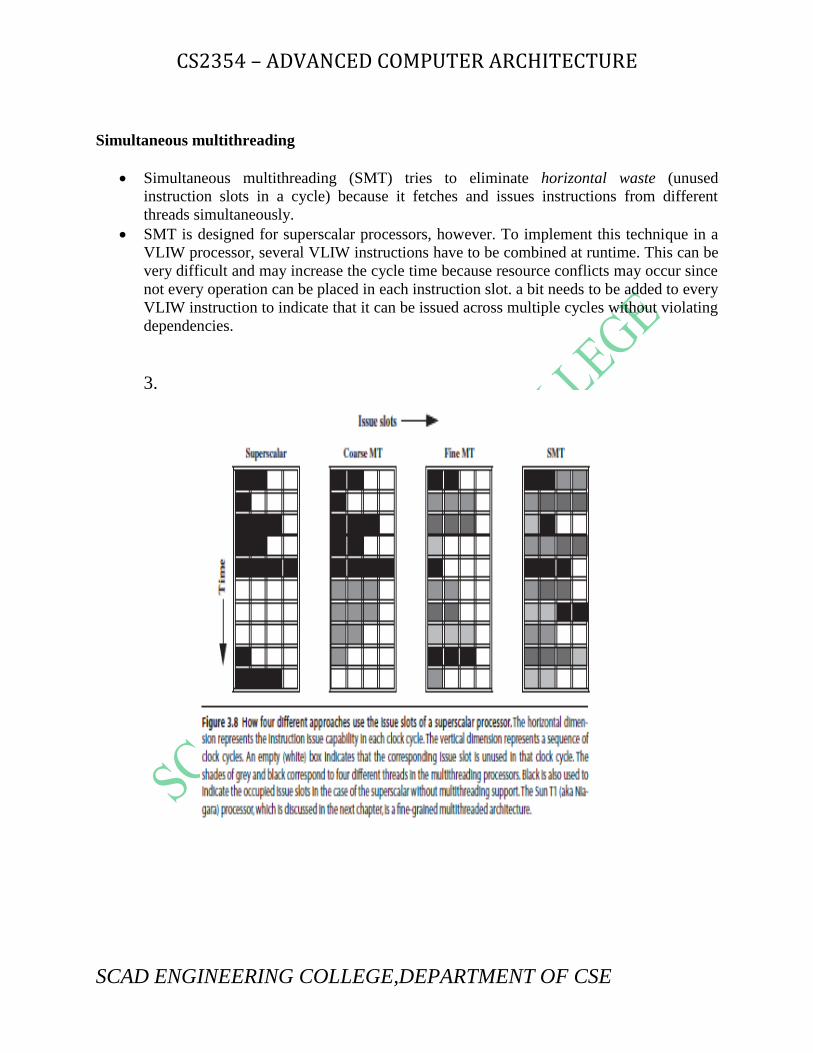
CS2354 – ADVANCED COMPUTER ARCHITECTURE
SCAD ENGINEERING COLLEGE,DEPARTMENT OF CSE
Simultaneous multithreading
Simultaneous multithreading (SMT) tries to eliminate horizontal waste (unused
instruction slots in a cycle) because it fetches and issues instructions from different
threads simultaneously.
SMT is designed for superscalar processors, however. To implement this technique in a
VLIW processor, several VLIW instructions have to be combined at runtime. This can be
very difficult and may increase the cycle time because resource conflicts may occur since
not every operation can be placed in each instruction slot. a bit needs to be added to every
VLIW instruction to indicate that it can be issued across multiple cycles without violating
dependencies.
3.
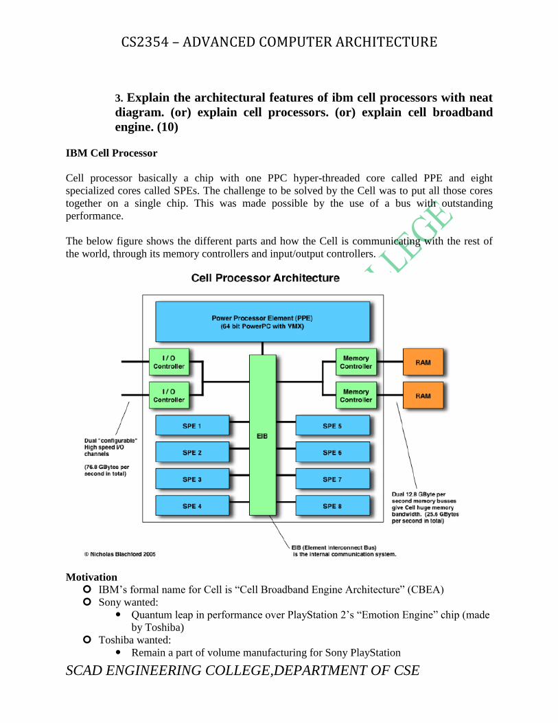
CS2354 – ADVANCED COMPUTER ARCHITECTURE
SCAD ENGINEERING COLLEGE,DEPARTMENT OF CSE
3. Explain the architectural features of ibm cell processors with neat
diagram. (or) explain cell processors. (or) explain cell broadband
engine. (10)
IBM Cell Processor
Cell processor basically a chip with one PPC hyper-threaded core called PPE and eight
specialized cores called SPEs. The challenge to be solved by the Cell was to put all those cores
together on a single chip. This was made possible by the use of a bus with outstanding
performance.
The below figure shows the different parts and how the Cell is communicating with the rest of
the world, through its memory controllers and input/output controllers.
Motivation
IBM‘s formal name for Cell is ―Cell Broadband Engine Architecture‖ (CBEA)
Sony wanted:
Quantum leap in performance over PlayStation 2‘s ―Emotion Engine‖ chip (made
by Toshiba)
Toshiba wanted:
Remain a part of volume manufacturing for Sony PlayStation

CS2354 – ADVANCED COMPUTER ARCHITECTURE
SCAD ENGINEERING COLLEGE,DEPARTMENT OF CSE
IBM wanted:
A piece of the PlayStation 3 pie
A second try at network processor architecture
Something reusable, applicable far beyond PlayStation
Cell is a microprocessor architecture jointly developed by Sony, Sony Computer
Entertainment, Toshiba, and IBM, an alliance known as "STI".
APPLICATIONS OF CELL PROCESSORS:
Application domains
Graphics Rendering
DSP & Multimedia Processing
Cryptography
Physics simulations
Matrix math and other scientific processing
Each Cell SoC contains:
Conventional processor (PPE), for control and a lightweight OS
2-way SMT, 2-way superscalar in-order Power core
Multiple Synergistic Processing Elements (SPEs)
These are execution engines for RPC of a software-cell
DMA interface to memory and I/O
Element Interconnect Bus (EIB), actually a ring bus
Each SPE contains:
128 registers, 128 bits wide in unified regfile (2Kbytes of registers!)
256 Kbytes local memory
4 SIMD integer pipelines/ALUs
4 SIMD floating point pipelines/FPUs
Power Processor Element (PPE)
The PPE is a 64 bit, "Power Architecture―
capable of running POWER or PowerPC binaries
Extended Vector Scalar Unit (VSU)
The PPE is
In-order
Dual threaded
Dual Issue
Synergistic Processing Elements
An SPE is a self contained vector processor (SIMD) which acts as a co-processor
SPE‘s ISA a cross between VMX and the PS2‘s Emotion Engine.
In-order (again to minimize circuitry to save power)
Statically scheduled (compiler plays big role)
Also no dynamic prediction hardware (relies on compiler generated hints)

CS2354 – ADVANCED COMPUTER ARCHITECTURE
SCAD ENGINEERING COLLEGE,DEPARTMENT OF CSE
Each SPE consists of:
128 x 128 register
Local Store (SRAM)
DMA unit
FP, LD/ST, Permute, Branch Unit (each pipelined)
SPE Local Store
Each SPE has local on-chip memory at Local Store(LS)
serves a secondary register file (not as cache)
Avoids coherence logic needed caches as well cache miss penalty
Is mapped into memory map of the processor allow LS to LS transactions
128 bit instruction fetch, load and store operation
7 out of every 8 cycles
Data/instructions are transferred between LS and system memory/other SPE‘s LS
using DMA unit
128 bytes at a time(transfer rate of 0.5 terabytes/sec)
DMA transactions are coherent

CS2354 – ADVANCED COMPUTER ARCHITECTURE
SCAD ENGINEERING COLLEGE,DEPARTMENT OF CSE
The PPE is made out of two main units:
1. The Power Processor Unit, usually denoted as the PPU. It is the processing part of the PPE
and is
composed of:
– A full set of 64-bit PowerPC registers.
– 32 128-bit vector multimedia registers.
– a 32KB L1 instruction cache.
– a 32KB L1 data cache.
– All the common components of a ppc processors with vector/SIMD extensions (instruction
control unit, load and store unit, fixed-point integer unit, floating-point unit, vector unit, branch
unit, virtual memory management unit).
The PPU is hyper-threaded and supports 2 simultaneous threads. All architectural and special
purpose registers are duplicated, except those dealing with system-level resources, such as
logical partitions, memory-control and thread-control. On the non-architectural side, most
resources are shared, except for very small resources, or those offering critical performance
improvement with multi-threaded applications.
2.The Power Processor Storage Subsystem (PPSS). It handles all memory requests from the PPE
and
requests made to the PPE by other processors or I/O devices. It is composed of:
– A unified 512-KB L2 instruction and data cache.
– Various queues
– A bus interface unit that handles bus arbitration and pacing on the Element Interconnect Bus
The SPEs
Each Cell chip has 8 Synergistic Processor Elements. These are usually referred to as the SPEs.
They are 128-bit RISC processor which are specialized for data-rich, compute-intensive SIMD
applications. They consist of two main units.
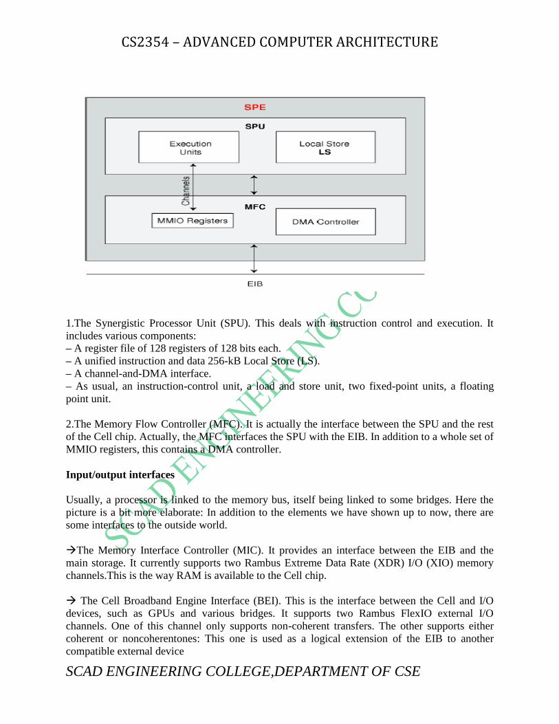
CS2354 – ADVANCED COMPUTER ARCHITECTURE
SCAD ENGINEERING COLLEGE,DEPARTMENT OF CSE
1.The Synergistic Processor Unit (SPU). This deals with instruction control and execution. It
includes various components:
– A register file of 128 registers of 128 bits each.
– A unified instruction and data 256-kB Local Store (LS).
– A channel-and-DMA interface.
– As usual, an instruction-control unit, a load and store unit, two fixed-point units, a floating
point unit.
2.The Memory Flow Controller (MFC). It is actually the interface between the SPU and the rest
of the Cell chip. Actually, the MFC interfaces the SPU with the EIB. In addition to a whole set of
MMIO registers, this contains a DMA controller.
Input/output interfaces
Usually, a processor is linked to the memory bus, itself being linked to some bridges. Here the
picture is a bit more elaborate: In addition to the elements we have shown up to now, there are
some interfaces to the outside world.
The Memory Interface Controller (MIC). It provides an interface between the EIB and the
main storage. It currently supports two Rambus Extreme Data Rate (XDR) I/O (XIO) memory
channels.This is the way RAM is available to the Cell chip.
The Cell Broadband Engine Interface (BEI). This is the interface between the Cell and I/O
devices, such as GPUs and various bridges. It supports two Rambus FlexIO external I/O
channels. One of this channel only supports non-coherent transfers. The other supports either
coherent or noncoherentones: This one is used as a logical extension of the EIB to another
compatible external device

CS2354 – ADVANCED COMPUTER ARCHITECTURE
SCAD ENGINEERING COLLEGE,DEPARTMENT OF CSE
Element Interconnect Bus
Connects various on chip elements
PPE , 8 SPEs, memory controller (MIC) & off-chip I/O interfaces
Data-ring structure with control of a bus
4 unidirectional rings but 2 rings run counter direction to other 2
Worst-case maximum latency is only half distance of the ring
4. Explain sun cmp architecture with neat diagram. (or) explain sun
niagara processor architecture. (10)
Niagara Overview
Supports 32 hardware threads
Each 4 threads are a group which shares a pipeline called Sparc pipe (total 8 Sparc pipes)
Each Sparc pipe has seprate I- and D-cache
Memory latency is hidden by thread switching at a cost of zero cycles
Shared 3MB L2 cache: 12-way set associative
Crossbar interconnect between pipes, L2 cache and other CPU shared resources with
bandwidth: 200 GB/s.
NIAGARA BLOCK DIAGRAM:

CS2354 – ADVANCED COMPUTER ARCHITECTURE
SCAD ENGINEERING COLLEGE,DEPARTMENT OF CSE
Sparc Pipeline
Single-issue, six-stage pipeline
fetch, thread select, decode, execute, memory, write back
Each pipeline supports 4 threads
Each thread has unique instruction and store buffer and register set
L1 cache, TLBs, FUs are shared
Pipeline registers are shared except the fetch and thread select stages

CS2354 – ADVANCED COMPUTER ARCHITECTURE
SCAD ENGINEERING COLLEGE,DEPARTMENT OF CSE
• Fetch:
• 64-entry ITLB access
• Two instructions per cycle with a pre-decode bit
• Thread select:
• Insert instructions to the buffer if resources are busy
• Decode:
• Decode and register file access
• Forwarding for data dependant instructions
• Execute:
• ALU, shift : single cycle
• mul, div : long latency and causes thread switch
• Memory:
• DTLB access
• Can cause a late trap which flushes all subsequently fetched instructions from the
same thread and a thread switch
• Write back
• Store the executed result onto the write back buffer.

CS2354 – ADVANCED COMPUTER ARCHITECTURE
SCAD ENGINEERING COLLEGE,DEPARTMENT OF CSE
SPARC PIPELINE:
Thread Selection Policy
Switch every cycle
Least recently used thread has high priority
Speculative instructions (fetched after load) have low priority
Deselection of threads can happen because of long latency instructions like mul and div
or by traps discovered later as in cache miss

CS2354 – ADVANCED COMPUTER ARCHITECTURE
SCAD ENGINEERING COLLEGE,DEPARTMENT OF CSE
Integer Register File
3 read ports
2 write ports
Register window implementation
A window has ins, outs and locals
Each thread has 8 windows
A new window is added by procedure calls, slide up
Procedure return, slide down
Divided into working set and architectural set
Working set is implemented by fast register file cells
Architectural consists of SRAM cells
Sets are linked by a transfer port
Window change triggers thread switch
Threads share the read circuit but not the registers

CS2354 – ADVANCED COMPUTER ARCHITECTURE
SCAD ENGINEERING COLLEGE,DEPARTMENT OF CSE
INTEGER REGISTER FILE:
Memory
L1 I-cache is 16KB 4-way set associative with block size of 32B
Random replacement policy
L1 D-cache is 8KB 4-way set associative with block size of 16B write through policy
Simple coherence protocol
L2 implements write back policy
Niagara Summary
Designed for power
Requires no special compiler
Exploits TLP
Useful for client-server applications
Implements fine-grain multithreading and CMP
CS2354 – ADVANCED COMPUTER ARCHITECTURE
SCAD ENGINEERING COLLEGE,DEPARTMENT OF CSE
5. Explain simultanous multi-threading concept for converting thread
level parallelism into instruction level parallelism. (8)
Simultaneous multithreading (SMT) is a variation on multithreading that uses the resources of a multiple-issue, dynamically scheduled processor to exploit TLP at the same time it exploits ILP. The key insight that motivates SMT is that modern multiple-issue processors often have more functional unit parallelism available.
In the SMT case, TLP and ILP are exploited simultaneously, with multiple threads using the
issue slots in a single clock cycle. Ideally, the issue slot usage is limited by imbalances in the
resource needs and resource availability over multiple threads.
As mentioned earlier, simultaneous multithreading uses the insight that a dynamically scheduled
processor already has many of the hardware mechanisms needed to support the integrated
exploitation of TLP through multithreading. In particular, dynamically scheduled superscalars
have a large set of virtual registers that can be used to hold the register sets of independent
threads (assuming separate renaming tables are kept for each thread). Because register renaming
provides unique register identifiers, instructions from multiple threads can be mixed in the data
path without confusing sources and destinations across the threads.
Design Challenges in SMT
Because a dynamically scheduled superscalar processor is likely to have a deep pipeline,
SMT will be unlikely to gain much in performance if it were coarse grained. Since SMT makes
sense only in a fine-grained implementation, we must worry about the impact of fine-grained
scheduling on single-thread performance.
This effect can be minimized by having a preferred thread, which still permits
multithreading to preserve some of its performance advantage with a smaller compromise in
single-thread performance.
Unfortunately, mixing many threads will inevitably compromise the execution time of
individual threads. Similar problems exist in instruction fetch. To maximize single-thread
performance, we should fetch as far ahead as possible in that single thread and always have the
fetch unit free when a branch is miss-predicted and a miss occurs in the prefetch buffer.
Unfortunately, this limits the number of instructions available for scheduling from other threads,
reducing throughput.
There are a variety of other design challenges for an SMT processor, including the following:

CS2354 – ADVANCED COMPUTER ARCHITECTURE
SCAD ENGINEERING COLLEGE,DEPARTMENT OF CSE
_ Dealing with a larger register file needed to hold multiple contexts
_ Not affecting the clock cycle, particularly in critical steps such as instruction issue, where more
candidate instructions need to be considered, and in instruction completion, where choosing what
instructions to commit may be challenging
_ Ensuring that the cache and TLB conflicts generated by the simultaneous execution of multiple
threads do not cause significant performance degradation In viewing these problems, two
observations are important. First, in many cases, the potential performance overhead due to
multithreading is small, and simple choices work well enough. Second, the efficiency of current
superscalars is low enough that there is room for significant improvement, even at the cost of
some overhead.
The IBM Power5 used the same pipeline as the Power4, but it added SMT support. In adding
SMT, the designers found that they had to increase a number of structures in the processor so as
to minimize the negative performance consequences from fine-grained thread interaction. These
changes included the following:
Increasing the associativity of the L1 instruction cache and the instruction address translation
buffers
_ Adding per-thread load and store queues
_ Increasing the size of the L2 and L3 caches
_ Adding separate instruction prefetch and buffering
_ Increasing the number of virtual registers from 152 to 240
_ Increasing the size of several issue queues
Because SMT exploits thread-level parallelism on a multiple-issue superscalar, it is most likely
to be included in high-end processors targeted at server markets.
In addition, it is likely that there will be some mode to restrict the multithreading, so as to
maximize the performance of a single thread.
Potential Performance Advantages from SMT
A key question is, How much performance can be gained by implementing SMT?
When this question was explored in 2000–2001, researchers assumed that dynamic superscalars
would get much wider in the next five years, supporting six to eight issues per clock with
speculative dynamic scheduling, many simultaneous loads and stores, large primary caches, and
four to eight contexts with simultaneous fetching from multiple contexts.

CS2354 – ADVANCED COMPUTER ARCHITECTURE
SCAD ENGINEERING COLLEGE,DEPARTMENT OF CSE
UNIT-V
PART-A
1. What is software and hardware multithreading?
Software multithreading is piece of software that is aware of more than one
core/processor, and can use these to be able simultaneously complete multiple tasks.
Hardware multithreading is a hardware that is aware of more than one core/processors
and can use these to be able simultaneously completes multiple threads.
2. Write short note on SMT.
Simultaneous multithreading is a technique for improving the overall efficiency of
superscalar CPU‘s with hardware multithreading. SMT permits multiple independent
threads of execution to better utilize the resources provided by modern processor
architectures.
3. List the design challenges of SMT.
Larger register file needed to hold multiple contexts.
Not affecting clock cycle time, especially its,
o Instruction issue: more candidate instructions need to be considered.
o Instruction completion: choosing which instructions to commit may be
challenging.
Ensuring that cache and TLP conflicts generated by SMT do not degrade
performance.
4. Define CMP.
Chip level multiprocessing(CMP or multi-core): integrates two or more independent
cores into a single package composed of a single integrated circuit, called a die, or more
dies packaged, each executing threads independently.
5. Define chip multithreading:
Chip multithreading is defined as the combination of chip multiprocessing and the
hardware multithreading.
Chip multithreading is the capability of a processor to process multiple software threads
and simultaneous Hardware threads of execution.
6. Define multicore processors.
A multicore design in which a single physical processor contains the core logic of more
than one processor.

CS2354 – ADVANCED COMPUTER ARCHITECTURE
SCAD ENGINEERING COLLEGE,DEPARTMENT OF CSE
7. What is heterogeneous multicore processor?
The architecture consists of a chip-level multi-processors with multiple, processor cores.
These cores all execute the same instruction set, but include significantly different
resources and achieve different performance and energy efficiency on the same
application.
8. List out the advantages of heterogeneous multicore processors.
More efficient adaptation to application diversity.
Applications place different demands on different architectures.
A more efficient use of die area for a given thread-level parallelism.
Chip level multiprocessors with a mix of cores.
9. What is IBM Cell processor?
Cell is a microprocessor architecture jointly developed by sony, sony computer
entertainment, Toshiba and IBM, an alliance known as ―STI‖. The architectural design
and first implementation were carried out at the STI design center in Austin, Texas over
four-year period.
10. List out the components of cell processors.
External input and output structures
The main processor called the Power Processing Element(PPE)
Eight fully functional co-processors called the Synergistic Processing elements or SPE‘s.
A specialized high bandwidth circular data bus connecting the PPE.

CS2354 – ADVANCED COMPUTER ARCHITECTURE
SCAD ENGINEERING COLLEGE,DEPARTMENT OF CSE
11. What are the components of SPE?
Synergistic processor unit(SPU)
Memory flow controller (MFC)
12. What is memory flow controller?
The memory flow controller is the interface between the SPU and the rest of the cell chip.
13. State fine grained multi-threading.
Switches between threads on each instructions, causing the execution of multiple threads
to be interleaved.
Usually done in a round robin fashion, skipping any stalled threads.
CPU must be able to switch threads every clock.
14. List Advantages of coarse grain multithreading.
It is hard to overcome throughput losses from shorter stalls, due to pipeline start-up costs.
Since CPU, issues instruction from 1 thread, when a stall occurs, the pipeline must be
emptied or frozen.
New thread must fill pipeline before instruction can complete.
15. Define coarse grain multithreading.
It switches thread only on costly stalls, such as L2 cache misses.