department of physics and astronomy university of heidelberg · the branching ratio br(µ+...
TRANSCRIPT

Department of Physics and AstronomyUniversity of Heidelberg
Bachelor Thesis in Physicssubmitted by
Jens Kroger
born in Lubbecke (Germany)
2014


Data Transmission at High Ratesvia Kapton Flexprints for the Mu3e Experiment
This Bachelor Thesis has been carried out byJens Kroger
at thePhysikalisches Institut Heidelberg
under the supervision ofProf. Dr. Andre Schoning


AbstractThe Mu3e experiment is aiming to search for the neutrinoless muon decay µ+ → e+e−e+
with a sensitivity of one in 1016 decays or better. This decay is lepton flavour violatingand strongly suppressed within the Standard Model. Therefore, even a single decaysignal would be a clear hint for new physics.
The concept of the Mu3e experiment is to achieve a very good momentum and timeresolution and an excellent vertex reconstruction to suppress background to a sufficientlevel. Since the decay electrons have a low energy up to 53 MeV, multiple Coulombscattering is the dominating limiting factor for the momentum and vertex resolution.Therefore, the material budget inside the detector region must be kept at a minimum.To achieve this, pixel detectors with a thickness of only 50 µm will be used whichare carried by a Kapton foil support structure. The pixel detectors shall be linked tofront-end FPGAs via ultra-thin Kapton flexprints.
The production and performance tests of self-manufactured Kapton flexprints arethe main scope of this thesis. It has been shown that flexprints with a trace width of120 µm and a trace separation of 110 µm can be manufactured reliably with a laserplatform available at the Heidelberg University. In addition, bit error rate tests havebeen performed which resulted in bit error rates below O(10−15) for 17 parallel channelsat a transmission rate of 800 Mbit/s each. Moreover, eye diagrams have been analyzedto understand which factors mainly affect the signal quality.
ZusammenfassungDas Mu3e-Experiment hat zum Ziel, den neutrinolosen Myon-Zerfall µ+ → e+e−e+ miteiner Genauigkeit von einem in 1016 Zerfallen oder besser zu suchen. Dieser Zerfall istleptonzahlverletzend und damit im Standardmodell so stark unterdruckt, dass selbstein einziger gemessener Zerfall ein klarer Hinweis auf neue Physik ware.
Das Konzept des Mu3e-Experiments ist es, eine sehr gute Impuls- und Zeitauflosungund Vertexrekonstruktion zu erreichen, um den Untergrund ausreichend stark zu unter-drucken. Da die Zerfallselektronen eine niedrige Energie von bis zu 53 MeV haben, isthauptsachlich Coulomb-Vielfachstreuung der limitierende Faktor fur die Impuls- undVertexauflosung. Deshalb soll innerhalb des Detektors so wenig Material wie moglichverbaut werden. Um dies zu erreichen, sollen Pixeldetektoren mit einer Dicke von ledig-lich 50 µm verwendet werden, die von einer Struktur aus Kaptonfolie getragen werden.Die Daten werden uber ultradunne Kaptonflexprints zu Front-End FPGAs ubertragen.
Die Herstellung sowie Performance-Tests selbsthergestellter Kapton-Flexprints sinddie Schwerpunkte dieser Arbeit. Es konnte gezeigt werden, dass Flexprints mit Lei-terbahnbreiten von 120 µm und Abstanden von 110 µm zuverlassig mit einer Laser-plattform an der Universitat Heidelberg hergestellt werden konnen. Zusatzlich sindFehlerraten-Tests durchgefuhrt worden, die Werte unter O(10−15) fur 17 parallele Ka-nale bei einer Datenrate von je 800 Mbit/s ergeben haben. Daruber hinaus sind Augen-diagramme analysiert worden, um zu verstehen, welche Faktoren die Signalqualitat imWesentlichen beeinflussen.


Contents
I Theory & Background 1
1 Theoretical Background 21.1 The Standard Model . . . . . . . . . . . . . . . . . . . . . . . . . . . . . 2
1.1.1 The Elementary Particles . . . . . . . . . . . . . . . . . . . . . . 21.1.2 Muon Decays . . . . . . . . . . . . . . . . . . . . . . . . . . . . . 3
1.2 Experimental Situation . . . . . . . . . . . . . . . . . . . . . . . . . . . 4
2 The Mu3e Experiment 62.1 The Mu3e Experiment . . . . . . . . . . . . . . . . . . . . . . . . . . . . 6
2.1.1 The Signal Decay . . . . . . . . . . . . . . . . . . . . . . . . . . . 62.1.2 Background Decays . . . . . . . . . . . . . . . . . . . . . . . . . 72.1.3 Experimental Concept . . . . . . . . . . . . . . . . . . . . . . . . 82.1.4 The Readout Concept . . . . . . . . . . . . . . . . . . . . . . . . 102.1.5 The Muon Beam . . . . . . . . . . . . . . . . . . . . . . . . . . . 11
3 Basics of Data Transmission 133.1 Signals . . . . . . . . . . . . . . . . . . . . . . . . . . . . . . . . . . . . . 13
3.1.1 Low Voltage Differential Signaling . . . . . . . . . . . . . . . . . 133.1.2 Data Encoding . . . . . . . . . . . . . . . . . . . . . . . . . . . . 15
3.2 Transmission Lines . . . . . . . . . . . . . . . . . . . . . . . . . . . . . . 183.2.1 The Characteristic Impedance . . . . . . . . . . . . . . . . . . . 193.2.2 Microstrips . . . . . . . . . . . . . . . . . . . . . . . . . . . . . . 20
3.3 Signal Quality Checks . . . . . . . . . . . . . . . . . . . . . . . . . . . . 213.3.1 Bit Error Rate Tests (BERTs) . . . . . . . . . . . . . . . . . . . 223.3.2 Eye Diagrams . . . . . . . . . . . . . . . . . . . . . . . . . . . . . 23
II Measurements & Results 25
4 Manufacturing of Kapton Flexprints 264.1 The Laser Platform . . . . . . . . . . . . . . . . . . . . . . . . . . . . . . 264.2 Kapton . . . . . . . . . . . . . . . . . . . . . . . . . . . . . . . . . . . . 27
4.2.1 Physical Properties . . . . . . . . . . . . . . . . . . . . . . . . . . 274.2.2 Electrical Properties . . . . . . . . . . . . . . . . . . . . . . . . . 27
4.3 Aluminum . . . . . . . . . . . . . . . . . . . . . . . . . . . . . . . . . . . 294.4 Structure Sizes . . . . . . . . . . . . . . . . . . . . . . . . . . . . . . . . 30
4.4.1 Impedance Calculations . . . . . . . . . . . . . . . . . . . . . . . 30

4.4.2 Test Structures . . . . . . . . . . . . . . . . . . . . . . . . . . . . 314.5 Flexprint Cables . . . . . . . . . . . . . . . . . . . . . . . . . . . . . . . 34
4.5.1 Limitations . . . . . . . . . . . . . . . . . . . . . . . . . . . . . . 354.5.2 Obtaining Different Types of Microstrips . . . . . . . . . . . . . 374.5.3 Mechanical Properties . . . . . . . . . . . . . . . . . . . . . . . . 384.5.4 Blackening of the Kapton . . . . . . . . . . . . . . . . . . . . . . 39
5 Performance of BERTs 425.1 Hardware . . . . . . . . . . . . . . . . . . . . . . . . . . . . . . . . . . . 43
5.1.1 Field Programmable Gate Array . . . . . . . . . . . . . . . . . . 435.1.2 FPGA Development Board . . . . . . . . . . . . . . . . . . . . . 435.1.3 HSMC Flexprint Adapter Board . . . . . . . . . . . . . . . . . . 43
5.2 Software . . . . . . . . . . . . . . . . . . . . . . . . . . . . . . . . . . . . 455.2.1 Altera Quartus II . . . . . . . . . . . . . . . . . . . . . . . . . . . 455.2.2 ModelSim . . . . . . . . . . . . . . . . . . . . . . . . . . . . . . . 46
5.3 Firmware: BERT Implementation . . . . . . . . . . . . . . . . . . . . . 465.3.1 Data Generator . . . . . . . . . . . . . . . . . . . . . . . . . . . . 465.3.2 8b/10b Encoder . . . . . . . . . . . . . . . . . . . . . . . . . . . 475.3.3 LVDS Transmitter . . . . . . . . . . . . . . . . . . . . . . . . . . 475.3.4 LVDS Receiver . . . . . . . . . . . . . . . . . . . . . . . . . . . . 475.3.5 8b/10b Decoder . . . . . . . . . . . . . . . . . . . . . . . . . . . 475.3.6 Data Checker . . . . . . . . . . . . . . . . . . . . . . . . . . . . . 48
5.4 BERT Results . . . . . . . . . . . . . . . . . . . . . . . . . . . . . . . . . 49
6 Analysis of Eye Diagrams 516.1 Test Setup . . . . . . . . . . . . . . . . . . . . . . . . . . . . . . . . . . . 51
6.1.1 Tektronix DPO 7254C Digital Phosphor Oscilloscope . . . . . . . 526.1.2 Tektronix TDP3500 Differential Probe . . . . . . . . . . . . . . . 52
6.2 Eye Diagram Results . . . . . . . . . . . . . . . . . . . . . . . . . . . . . 536.2.1 Influence of the HSMC Flexprint Adapter Board . . . . . . . . . 536.2.2 Influence of the Cable Length . . . . . . . . . . . . . . . . . . . . 566.2.3 Influence of the Transmission Rate . . . . . . . . . . . . . . . . . 596.2.4 Influence of the Pre-Emphasis . . . . . . . . . . . . . . . . . . . . 606.2.5 Crosstalk between Trace Pairs . . . . . . . . . . . . . . . . . . . 616.2.6 Influence of the Microstrip Type . . . . . . . . . . . . . . . . . . 626.2.7 Influence of the Knee Length . . . . . . . . . . . . . . . . . . . . 64
III Conclusion & Outlook 67
7 Conclusion 687.1 Manufacturing of Kapton Flexprints . . . . . . . . . . . . . . . . . . . . 687.2 BERT Results . . . . . . . . . . . . . . . . . . . . . . . . . . . . . . . . . 697.3 Eye Diagram Results . . . . . . . . . . . . . . . . . . . . . . . . . . . . . 697.4 Recommendations . . . . . . . . . . . . . . . . . . . . . . . . . . . . . . 70

8 Outlook 718.1 Consequences for the Mu3e Experiment . . . . . . . . . . . . . . . . . . 71
8.1.1 Spatial Constraints . . . . . . . . . . . . . . . . . . . . . . . . . . 718.1.2 Transmission Errors . . . . . . . . . . . . . . . . . . . . . . . . . 72
8.2 Further Work . . . . . . . . . . . . . . . . . . . . . . . . . . . . . . . . . 73
List of Figures 74
List of Tables 75
Bibliography 76
Acknowledgements 80


Part I
Theory & Background

1 Theoretical Background
1.1 The Standard Model
1.1.1 The Elementary Particles
The Standard Model of particle physics (SM) [1] is a quantum field theory that com-prises the description of the smallest constituents of matter, the elementary particles, aswell as the electromagnetic, the weak, and the strong interaction. Only gravity cannotbe described. The SM was developed throughout the second half of the 20th centuryand has passed countless experimental tests until today. Especially the recent discoveryof a new particle, which is likely to be the long predicted Higgs boson, has given furthersupport to this theory [2, 3].
According to the SM, the fundamental particles comprise six quarks, six leptons, andtheir corresponding anti-particles. Furthermore, there are four types of gauge bosonsand the Higgs boson (see Figure 1.1). The quarks and leptons form three generations.The first generation contains the up quark (u) and the down quark (d) with charges of+2/3 and -1/3 in units of the elementary charge, the electron (e−) and the electricallyneutral electron neutrino (νe).
The second and the third generation are also made up of a pair of quarks, a leptonand a neutrino. These are the charm quark (c) and the strange quark (s) together withthe muon (µ−) and the muon neutrino (νµ) in the second generation and the top quark(t), the bottom quark (b) together with the tau (τ) and the tau neutrino (ντ ) in thethird generation.
All quarks and leptons are spin 1/2 particles, i.e. they are fermions. The interactionbetween them is mediated by the gauge bosons which have spin 1. The eight gluonsare responsible for the strong interaction, the photon (γ) mediates the electromagneticforce and the Z0, W+ and W− go with the weak interaction.
In the SM, the neutrinos are considered to be massless. The so-called lepton flavournumber, i.e. the number of anti-leptons subtracted from the number of leptons of onegeneration, is a conserved quantity.
2

Figure 1.1: Particles described by the SM [4].
In spite of the great successes of the SM, observations have been made which cannotbe explained by this theory. Several experiments have observed neutrino oscillation,such as Super-Kamiokande [5], SNO [6], KamLAND [7], and Daya-Bay [8]. To ex-plain this mixing of the flavour eigenstates, the neutrinos need a non-vanishing mass,which is not foreseen in the SM. An extension by heavy right-handed neutrinos, calledνSM, yields consistent results with oscillation experiments [9]. Still it cannot be ex-plained why the neutrino masses are orders of magnitude smaller than those of the otherparticles. Moreover, νSM does not provide any explanation for the observed matter-antimatter-asymmetry, the origin of dark matter, or the existence three generationsof particles. These phenomena motivate theories beyond the Standard Model (BSM),such as supersymmetric theories (SUSY). In contrast to the SM, many of these predictflavour violating processes at an observable branching ratio.
1.1.2 Muon Decays
(Anti-)muons are unstable and have a mean lifetime of about 2.2 µs. The domina-ting decay in the SM is µ+ → e+νeνµ [1]. Considering neutrino mixing (and thereforeallowing lepton flavour violation) the muon decay can also be realised without outgoingneutrinos (see Figure 1.2b).
3

(a) Dominant SM muon decay: the Micheldecay.
(b) Strongly suppressed decay µ+ → e+e+e−
with neutrino oscillation.
Figure 1.2: Feynman diagrams of possible SM muon decays [10].
As the W+ mass of 80.4 GeV/c2 is much higher than the neutrino mass differences(< 2 eV) [1], the decay µ+ → e+e−e+ is strongly suppressed with a branching ratio(BR) below 10−54 [11] and thus unobservable.
There are BSM theories that predict a much higher BR for this decay introducingnew tree couplings (see Figure 1.3a) or loop contributions with new particles (see Figure1.3b). Therefore, any observation of this process would be a clear hint for new physics.
(a) Tree diagram involving anunknown particle X.
(b) Penguin diagram with a SUSYloop.
Figure 1.3: Feynman diagrams of possible BMS muon decays [10].
1.2 Experimental Situation
Since 1953 experiments are performed to search for lepton flavour violation in muondecays (see Figure 1.4) [11–13]. Until today only upper limits for the branching ratioswere found. The current upper limit for the µ+ → e+e+e− decay is set by the SIN-DRUM experiment [14], whereas the best measurement for µ+ → e+γ was performedby the MEG experiment [15].
4

SINDRUM
From 1983-86, the SINDRUM experiment was in operation at the Paul-Scherrer-Institut(PSI) in Villigen, Switzerland. Because no signal event was detected, an upper limit forthe branching ratio BR(µ+ → e+e+e−) < 10−12 could be set at 90% confidence level(CL) [14].
In the experiment, which was placed inside a solenoid magnetic field of 0.33 T, muonswith a momentum of about 28 MeV/c were stopped in a hollow double-cone target.The decay products were measured by five tracking layers of multiwire proportionalchambers and an array of scintillators for triggering and timing measurements.
MEG
To search for the LFV decay µ+ → e+γ the MEG experiment uses a drift chamber todetect the positron and a liquid xenon calorimeter for the photon. It has been runningat PSI since 2008 and is currently being upgraded to MEG II [16]. The current upperlimit is BR(µ+ → e+γ) < 5.7 · 10−13 at 90% CL [15].
Figure 1.4: The history of LFV muon decay experiments, adapted from [11].
5

2 The Mu3e Experiment
2.1 The Mu3e Experiment
Mu3e is an experiment to search for the lepton flavour violating decay µ+ → e+e+e− [17].It is aiming to be sensitive for better than one signal decay in 1016 muon decays. Thiswould increase the sensitivity by four orders of magnitude compared to the currentupper limit given by SINDRUM.
To perform the experiment on a reasonable time scale, a very high muon stopping rateof O(109/s) is needed. Consequently, the main challenges for the detector design are tohandle high data rates and to have a very efficient accidental background suppression.
For the latter, a very precise vertex fitting< 200 µm as well as a momentum resolutionbelow 0.5 MeV/c and an excellent time resolution < 100 ps are needed.
The main limiting factors for the momentum and vertex resolution is multiple Coulombscattering of the decay electrons in the detector material. Thus, the material budget ofthe detector must be as low as possible.
2.1.1 The Signal Decay
The muons will be stopped in a target to decay at rest. Thus the total momentum ofthe decay electrons is vanishing:
~ptot =3∑i=1
~pi = 0. (2.1)
The decay at rest constrains the total energy to be equal to the rest mass of themuon:
Etot =3∑i=1
Ei = mµ · c2 ≈ 105.7 MeV. (2.2)
In summary, the signal decay is given by three electrons with a vanishing total mo-mentum and an energy between mec
2 ≈ 0.5 MeV and 1/2 ·mµ ≈ 53 MeV coming froma common vertex and being coincident in time.
6

2.1.2 Background Decays
Any background is due to fake signals that can be divided into two groups: internalconversion and random combinatorial background.
Internal Conversion
Internal conversion is the decay µ+ → e+e−e+νeνµ (see Figure 2.1) which has a branch-ing ratio of 3.4 · 10−5 [1]. Here, the emitted photon immediately converts into anelectron-positron pair.
Considering vertex and timing, this decay is indistinguishable from the signal decay.The only difference is a fraction of momentum and energy carried away by the neutrinoswhich cannot be detected. This clarifies the need for a very high momentum resolution.If both neutrinos have a vanishing momentum, this decay looks exactly as the signaldecay. This is the only irreducible background.
In Figure 2.2, the branching ratio for the internal conversion as a function of themissing energy is plotted. The missing energy corresponds to the difference of mµ · c2
and the energy carried away by the electrons which is measured. To suppress thisbackground sufficiently, an energy resolution below 1 MeV is needed.
Figure 2.1: The internal conversion decayµ+ → e+e−e+νeνµ [18].
Figure 2.2: Branching ratio for theinternal conversion as a function
of the missing energy [19].
Random Combinatorial Background
Due to a limited spatial resolution two nearby vertices cannot be properly separated ifthey are too close together.
As can be seen in Figure 2.3a two positrons from the dominant Michel decay µ+ →e+νeνµ (see Figure 1.2a) can be accidentally combined with an electron, for exam-ple produced by photon conversion or Bhabha scattering. Another possibility is the
7

(a) Accidental combination of two Michelpositrons with an electron from pair
production.
(b) Accidental combination of anelectron-positron pair from internalconversion with a Michel positron.
Figure 2.3: Possible combinatorial background.
combination of an electron and a positron from the internal conversion process µ+ →e+e−e+νeνµ with a Michel positron (see Figure 2.3b).
2.1.3 Experimental Concept
As discussed above, for an efficient background suppression high rate capabilities aswell as excellent spatial, time and momentum resolution are crucial.
The basic concept of the Mu3e experiment is to measure the momenta of the muondecay electrons in a solenoidal magnetic field of 1 T with a silicon pixel detector.Because multiple Coulomb scattering in the detector material is the limiting factorfor the momentum resolution, minimizing the material budget below 1h of radiationlength per layer in the active detector region is essential.
In Figure 2.4 a schematic view of the detector design is shown. The incoming muonbeam will be stopped in a hollow double-cone made of aluminum to decay at rest. Fourlayers of very thin pixel detectors are arranged in two double layers (black) to trackthe decay electrons. Furthermore, scintillating fibres (grey) are used for precise timingmeasurements. As the experiment is placed in a magnetic field, the electrons are curledback and detected again by another double layer of pixel sensors. Finally, they arestopped in scintillating tiles which again yield precise timing information.
Pixel Detector The Mu3e pixel detector consists of High-Voltage Monolithic ActivePixel Sensors (HV-MAPS) with a pixel size of 80×80 µm2. The chips are thinned down
8

Figure 2.4: Schematic drawing of the detector design. The blue and the red linesrepresent recurling positrons and an electron from a signal decay. On theright side: view along the beam axis [17].
to 50 µm and have a size of 1 × 2 cm2 in the inner layers, and 2 × 2 cm2 in the outerand the recurl layers [20, 21]. With 275 million pixels an area of more than 1 m2 willbe covered.
In contrast to the classical MAPS technology, the ionization charges are collected bydrift due to an applied high voltage (HV). This leads to a much faster charge collectioncompared to the diffusion process in MAPS. In addition, the radiation tolerance isimproved. Several prototype chips are tested [22–24].
The chips will be glued on a self-supporting Kapton structure (see Figure 2.5) witha thickness of 25 µm and wire bonded to Kapton flexprint cables for power supply andreadout. The triggerless readout will be done by zero-suppressed serial 800 Mbit/s LowVoltage Differential Signaling (LVDS) (see Subsection 3.1.1) [25–27].
Fibre Detector The pixel detector will be read out in 50 ns time frames. Due to thehigh decay rate of 2 ·109/s about 100 decays per frame occur in the detector acceptance.Thus, a more precise timing measurement is needed and provided by the scintillatingfibre detector.
The fibre detector consists of two or three layers of scintillating fibres with a diameterof 250 µm forming ribbons. The light produced by scintillation will be read out witharrays of silicon photo-multipliers (SiPM) mounted at both ends of the ribbons [28].
9

Figure 2.5: First mechanical prototype of the Kapton support structure for the innertwo layers (length: 12 cm).
Tile Detector The third sub-detector is a scintillating detector consisting of 7.5 ×7.5× 5 mm3 tiles which are also read out by SiPMs. It will be placed right underneaththe recurl pixel double-layer.
As this is the last measurement of the decay particles more material can be used.This leads to a detection efficiency close to 100% and a very high timing accuracy below100 ps [29].
Detector Environment As mentioned above, the whole detector will be placed ina solenoidal homogeneous magnetic field of 1 T to bend the electron tracks. Thefront-end electronics will be placed directly on the muon beam pipe. For cooling, thewhole detector volume will be filled with a circulating helium atmosphere. In addition,channels in the Kapton support structure will be flushed with gaseous helium for coolingof the pixel detectors [30–32].
2.1.4 The Readout Concept
In Figure 2.6, a schematic of the Mu3e readout chain is shown. The pixel sensors aswell as the fibre and tile detectors will be connected to so-called front-end FPGAs (fieldprogrammable gate arrays, see Subsection 5.1.1). These FPGAs will be located directlyon the beam pipe inside the detector.
10

The connection between the pixel detectors and the front-end FPGAs will be realizedby serial 800 Mbit/s LVDS links (low voltage differential signalling, see Subsection 3.1.1)which will consist of tiny aluminum traces on Kapton. The manufacturing and perfor-mance tests of these so-called flexprints are the main scope of this work (see Chapter 4).
From the front-end FPGAs, the data will be sent out from the detector to FPGA-driven readout boards via high-speed optical links. Thus, a galvanic separation isguaranteed.
The data from the readout boards will then be transmitted via high-speed opticallinks to a GPU (graphical processing unit) filter farm where an online track and eventreconstruction will be performed. Events of interest will then be sent to a data collectionserver which stores them in a mass storage system.
2.1.5 The Muon Beam
As an extremely high number of muons needs to be stopped to decay, a very intensemuon beam is required. Therefore, the Mu3e experiment is supposed to be run at thePaul-Scherrer-Institut (PSI) in Switzerland, which operates the world’s most intensemuon source.
The PSI operates a cyclotron to accelerate protons which hit a carbon target, wherepions are created as secondary particles. Slow pions decay immediately into muonswhich are collected in the πE5 beamline so that a low momentum muon beam with arate of 2 · 108 1/s is provided for a first phase of the Mu3e experiment.
In a second phase, the Mu3e experiment aims to improve the sensitivity by anotherorder of magnitude. Therefore, a more intense muon beam is needed. Such a beamcould be provided by the planned High intensity Muon Beamline (HiMB) for whichthe protons from the cyclotron mentioned above will be shot on the Swiss SpallationNeutron Source (SINQ) target [33]. There, a high number of muons will be created asa by-product and could be collected by the HiMB to provide a muon rate of 2 · 109 1/s.
11

Figure 2.6: Schematic of the Mu3e readout chain consisting of three stages.
12

3 Basics of Data Transmission
Data transmission is the transport of information from one point to another wherebythe data is represented by a physical signal [34].
3.1 Signals
A signal is the time-dependent magnitude of an observable. Electrical signals can berepresented by a voltage or current. Also electromagnetic waves (optical or radio) canbe used. To have an effective content of information, the time evolution of the signalmust be unpredictable because otherwise the receiver can foresee incoming data whichmakes the transmission redundant [35].
Analogue Signals
An analogue signal is continuous in time and amplitude. In principle, every classicalphysical observable like brightness, temperature, or pressure can be understood as ananalogue signal. Mathematically, it can be described by a smooth function of time [36].
Digital Signals
On the contrary, a digital signal consists of a sequence of discrete values. That is tosay, there is only a limited set of well distinguishable values which can be attainedand which are furthermore only defined at periodic points in time. An analogue signalcan be transformed into a digital signal by quantisation and sampling in constant timeintervals [36].
In electronics, it is common to use merely the two Boolean values 0 (false) and 1(true) which are associated to two logic voltage levels or the transitions between those.The binary numeral system provides the theoretical basis to use binary codes (sequencesof zeros and ones) for digital information processing of all kinds.
3.1.1 Low Voltage Differential Signaling
Low Voltage Differential Signaling (LVDS) is an interface standard for high-speeddata transmission. It describes the physical layer which means that it only comprises
13

Figure 3.1: Schematic drawing of a basic LVDS circuit. Also, the field coupling of thedifferential pair is shown [38].
the mechanical and electronic components, i.e. the hardware, of a physical link but noencoding schemes or protocols [37].
Figure 3.1 shows the architecture of an LVDS link. A current source is injecting aconstant current of 3.5 mA into the circuit. Transistors work as switches to controlthe direction of the current towards the receiver. At the receiver side, there is a 100 Ωterminating resistor at which a voltage of 350 mV drops according to Ohm’s law.
The receiver, which is a comparator with a transition threshold of about 50 mV,senses the polarity of the signal to determine the logic state being transmitted.
LVDS has the advantage of generating very low electromagnetic noise due to theclosely coupled wires. As they carry the same current in opposite directions, most ofthe radiation is cancelled. For the same reason, an LVDS link is relatively insensitiveto external electromagnetic noise because the noise will nearly equally affect both wiresand cancel out. This means that there is only very little cross-talk between adjacentwire pairs even if they are close to each other.
Another considerable advantage of LVDS is the low power consumption because ofthe low voltage and little radiative losses compared to other concepts of signaling. Thepower consumption is particularly low if it can be ensured by the transmitter side thatthere is no disparity, i.e. the number of ones equals the number of zeros transmitted,because in this case there is not even a net current averaged over time (see 8b/10bencoding below).
14
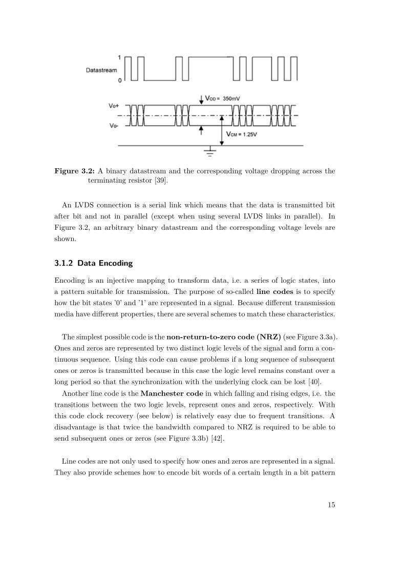
Figure 3.2: A binary datastream and the corresponding voltage dropping across theterminating resistor [39].
An LVDS connection is a serial link which means that the data is transmitted bitafter bit and not in parallel (except when using several LVDS links in parallel). InFigure 3.2, an arbitrary binary datastream and the corresponding voltage levels areshown.
3.1.2 Data Encoding
Encoding is an injective mapping to transform data, i.e. a series of logic states, intoa pattern suitable for transmission. The purpose of so-called line codes is to specifyhow the bit states ’0’ and ’1’ are represented in a signal. Because different transmissionmedia have different properties, there are several schemes to match these characteristics.
The simplest possible code is the non-return-to-zero code (NRZ) (see Figure 3.3a).Ones and zeros are represented by two distinct logic levels of the signal and form a con-tinuous sequence. Using this code can cause problems if a long sequence of subsequentones or zeros is transmitted because in this case the logic level remains constant over along period so that the synchronization with the underlying clock can be lost [40].
Another line code is the Manchester code in which falling and rising edges, i.e. thetransitions between the two logic levels, represent ones and zeros, respectively. Withthis code clock recovery (see below) is relatively easy due to frequent transitions. Adisadvantage is that twice the bandwidth compared to NRZ is required to be able tosend subsequent ones or zeros (see Figure 3.3b) [42].
Line codes are not only used to specify how ones and zeros are represented in a signal.They also provide schemes how to encode bit words of a certain length in a bit pattern
15

(a) The non-return-to-zero code: ones andzeros are represented by two logic levels of the
signal.
(b) The Manchester code: ones and zeros arerepresented by falling and rising edges
respectively.
Figure 3.3: The bit pattern ”11011000100” represented in two commonly used linecodes: the NRZ and the Manchester code [41].
with properties suiting the physical link [43]. Furthermore, additional information canbe contained for the following purposes:
• If there is no extra clock transmission line sending ”0101...” continuously, the clockhas to be recovered from the data stream (clock recovery). Therefore a hightransition rate between the logic levels is favourable.
• Some encoding schemes provide the possibility to send either data or a predefinedcontrol sequence of bits. If transmitting a continuous bit stream, control wordscan be used to identify bit packets (words). Thus, the bit stream can be cut intowords of a certain length.
• For some physical layers, like LVDS, it is desirable to have DC balance, i.e. tosend an equal number of ones and zeros to achieve a vanishing net current. Byan encoding scheme like 8b/10b this can be accomplished.
• A detection of transmission errors is possible if bit patterns are used forwhich a single bitflip yields an invalid word.
8b/10b Encoding
The disparity (dp) of a bit pattern is given by the difference in number of ones andzeros, counting ones as -1/2 and zeros as 1/2. If considering a continuous data stream,the running disparity (rd) is defined as the running sum over all previously trans-mitted words.
For 8 bit words encoded in 10 bits it is possible to ensure DC balance in a long run.That is because with 8 bits 28 = 256 words can be created, whereas with 10 bits thereare 210 = 1024 combinations. Regarding the restrictions that the 10 bit patterns shall
16

Word Data dp=-1 dp=+1 Word Data dp=-1 dp=+1
D.00 00000 100111 011000 D.16 10000 011011 100100D.01 00001 011101 100010 D.17 10000 100011D.02 00010 101101 010010 D.18 01010 010011D.03 00011 110001 D.19 01011 110010D.04 00100 110101 001010 D.20 01100 001011D.05 00101 101001 D.21 01101 101010D.06 00110 011001 D.22 01110 011010D.07 00111 111000 000111 D.23 10111 111010 000101D.08 01000 110001 000110 D.24 11000 110011 001100D.09 01001 100101 D.25 11001 100110D.10 01010 010101 D.26 11010 010110D.11 01011 110100 D.27 11011 110110 001001D.12 01100 001101 D.28 11100 001110D.13 01101 101100 D.29 11101 101110 010001D.14 01110 011100 D.30 11110 011110 100001D.15 01111 01011 101000 D.31 11111 101011 010100
K.28 11100 001111 110000
Table 3.1: 5b/6b encoding scheme. For several 5 bit words two different patterns withdisparity dp = ±1 exist. D.x mark the 25 = 32 possible data words, K.28 is acontrol word [26].
suffice a disparity of 0 or ±2 and never have more than five equal subsequent bits, 584of the possible 1024 combinations are left.
One way of implementing this concept has been developed by IBM in 1983 [44]. The8 bits of a word are split into two parts and are treated separately according to an 5b/6band an 3b/4b part (see Tables 3.1 and 3.2), respectively. During the data transmission,the running disparity is determined to control the combination of 6 bits and 4 bits beingused to satisfy the condition dp = 0 or dp = ±1.
Besides the advantage of DC balancing, this encoding scheme comprises some controlwords (so-called K-words) which do not encode data but can be used for clock recoveryand phase alignment before beginning to transmit user data or to bypass phases whenno actual data is transmitted to retain the synchronization. The K.28.7 word is ofparticular importance because it does not result from a single bit flip in the datastream.
17

Word Data dp=-1 dp=+1 K-Word Data dp=-1 dp=+1
D.x.0 000 1011 0100 K.x.0 000 1011 0100D.x.1 001 1001 K.x.1 001 0110 1001D.x.2 010 0101 K.x.2 010 1010 0101D.x.3 011 1100 0011 K.x.3 011 1100 0011D.x.4 100 1101 0010 K.x.4 100 1101 0010D.x.5 101 1010 K.x.5 101 0101 1010D.x.6 110 0110 K.x.6 110 1001 0110
D.x.P7 111 1110 0001 K.x.7 111 0111 1000D.x.A7 111 0111 1000
Table 3.2: 3b/4b encoding scheme. For several 2 bit words two different patterns withdisparity dp = ±1 exist. For D.x.7 either P7 or A7 is used to ensure that inthe resulting 10 bit pattern never more than five equal bits occur. The K.x.ywords can be combined with the K.28 word of Table 3.1 to form a controlword [26].
3.2 Transmission Lines
Only for direct and very low frequency alternating currents, electric wires can be char-acterized solely by their ohmic resistance. If the wavelength of a signal is in the orderof the length of the link, this simple model is not sufficient any more.
Instead, a description as a transmission line is appropriate. This comprises not onlythe resistance of the wire but also its capacitance and inductance (see Figure 3.4). Inplace of the total resistance R, the inductivity L and the capacitance C their normalized(i.e. per length dx) counterparts R′, L′ and C ′ are used. G′ represents the conductanceof the dielectric material between the transmission line and ground.
Within this model, a real wire is described as an infinite series of such elements.
Figure 3.4: Equivalent circuit diagram of an infinitesimally short piece of a transmis-sion line with normalized inductance L′ and resistance R′ coupled to groundvia G′ and C ′ [45].
18

3.2.1 The Characteristic Impedance
If the transmission line is homogeneous along its length, a single parameter is sufficientto describe its behaviour: the characteristic impedance Z0. It is equal to the ratioof the complex voltage and the complex current of a wave travelling along the line.
It can be shown (see [46]) that Z0 is given by
Z0 =
√R′ + iωL′
G′ + iωC ′. (3.1)
Note that Z0 is independent of the length of the transmission line. For an idealconducting material (R′ = 0) and an ideal dielectric (G′ = 0) or high frequencies(R′ iωL′ and G′ iωC ′) equation 3.1 reduces to
Z0 =
√L′
C ′, (3.2)
so that the characteristic impedance is also independent of the frequency. In suchcases, Z0 is not related to the ohmic resistance of a wire which causes an attenuation ofthe amplitude of a transmitted signal and is self-evidently dependent on the length ofthe transmission line. The characteristic impedance is merely a parameter to describea wire’s high-frequency behaviour.
When considering a pair of transmission lines with opposite current, which is the casefor LVDS, another quantity is of importance: the differential impedance Zdiff. It isdefined as the ratio of the differential voltage Vdiff and the current I1 on one line [47].
Due to an inductive coupling between the lines, a current I1 in one trace will causea current α · I1 in the second trace with α ∈ (0, 1) being the coupling constant. Acalculation, which can be found in [48], yields
Zdiff = 2Z0(1− α) . (3.3)
The differential impedance is of particular importance for reflections which occur ifwires or other electric components with different characteristic impedances are con-nected. The reflection coefficient Γ is given by
Γ = Zdiff,b − Zdiff,aZdiff,a + Zdiff,b
, (3.4)
where Zdiff,a and Zdiff,b correspond to two arbitrary connected components and Zdiff = R
in case of an ohmic terminating resistor. Γ is in the range of -1 to 1 and negative val-ues correspond to a reflection with a phase shift by π. Obviously, the characteristic
19

impedance of all components of an electric circuit should be matched as good as possi-ble to ensure proper signal propagation and minimize reflections [49].
3.2.2 Microstrips
Microstrips are a certain type of transmission lines which are commonly used on printedcircuit boards (PCBs) and flexprint cables (see Chapter 4). They are suited for signalsin the microwave range (300 MHz to 300 GHz).
Differential Microstips
A microstrip consists of a conducting trace which is separated from a ground (or otherconstant potential) plane by a dielectric layer called substrate. For LVDS links (seeSubsection 3.1.1) a pair of wires is needed. When designing a PCB, the trace width w,the trace separation s, the trace thickness t, and the dielectric thickness h, as well as thedielectric constant of the substrate εr (see Figure 3.5a) need to be taken into accountto match the impedance to the other electric components for minimal reflections.
Therefore, the following equation can be used for differential microstrips [50]. Thisapproximation is valid for ratios of w/h between 0.1 and 3.0.
Zdiff = 174√εr + 1.14
ln ( 5.98 · h0.8 · w + t
)(1− 0.48 · e−0.96 sh ) (3.5)
(a) Differential microstrips. (b) Coplanar striplines.
Figure 3.5: Profiles of two kinds of microstrips.
Coplanar Striplines
At first appearance, coplanar striplines seem to be very similar to differential microstrips(see Figure 3.5b), but there is a crucial difference when calculating the characteristicimpedance. This is because in case of the latter, there is a clear boundary condition forthe electric field surrounding the conducting traces due to the ground plane. Accordingto [51], the impedance Z0 of a coplanar stripline can be calculated by
Z0 = 120π√εeff
K(k0)K(k′0) , (3.6)
20

where εeff is an effective dielectric constant given by
εeff = 1 + (εr − 1) · 12K(k′)K(k)
K(k0)K(k′0) (3.7)
with K(•) being the elliptic integral of first kind and
k0 = s/2s/2 + w
, k′0 =√
1− k20 , (3.8)
k =tanh πs
4h
tanh πw+s/22h
, k′ =√
1− k2 . (3.9)
For practical purposes, α ≈ 0 and therefore Zdiff ≈ 2Z0 is assumed for coplanarstriplines within the scope of this thesis.
Typically, PCBs and flexprints with (differential) microstrips are produced in litho-graphic processes consisting of many steps in which multiple substrate and copper layersare assembled. An overview of typical dimensions of microstrips in standard and leadingedge processes is given in Table 3.3.
copper thickness t trace width w trace separation s dielectric thickness h
Multilayer PCB ≥ 50 µm ≥ 100 µm ≥ 100 µm ≥ 60 µm(standard process) [52]
Multilayer PCB approx. 25− 30 µm ≥ 75 µm ≥ 75 µm ≥ 60 µm(advanced process) [52]
Flexprint ≥ 5 µm ≥ 20 µm ≥ 25 µm ≥ 25 µm(leading edge) [53]
Table 3.3: Typical parameters for microstrips on PCBs and flexprints.
3.3 Signal Quality Checks
Once a physical link has been realized, it needs to be tested to ascertain how reliabledata can be transmitted. There are mainly two concepts which will be introduced inthe following.
21

3.3.1 Bit Error Rate Tests (BERTs)
A bit error rate test (BERT) is a method to determine the quality of a transmissionlink for digital data transmission. The bit error rate (BER) is the ratio of the numberof wrongly transmitted bits k and the total number of transmitted bits n and representsan estimation for the probability p for an error to occur if one bit is transmitted:
BER = p = # error bits# total bits = k
n(3.10)
In principle, a BERT can be realized by sending a deterministic datastream and com-paring the incoming bits to the expected pattern at the receiver side [25]. The exactarchitecture of the BERT used for this thesis is described in Chapter 5.
Mathematically, a BERT can be understood as a classical counting experiment. Asfor every transmitted bit there are two discrete results (false or correct), it obeys abinomial distribution. For data transmission at high rates, n becomes large withinseconds and the probability p for an error bit should be very small (p 1) due to a goodphysical link. Therefore, the binomial distribution converges to a Poisson distributionif µ := lim
n→∞p · n > 0 and the probability P (k) to find k error bits in a large number of
transmitted bits is given by
P (k) = µk
k! · e−µ . (3.11)
For large n, the Poisson distribution converges to a normal distribution so that thestandard deviation is given by σk =
√k. Thus, for the BER one gets
BER = k
n±√k
n. (3.12)
Upper BER Limit
If no error is detected, i.e. k = 0, an estimation for an upper limit of the BER mustbe found. In the following, a perfectly working data checker is assumed so that noerror counts occur accidentally, i.e. there is no background, and no error is overlooked.According to [54] and [55], a Bayesian approach with a flat prior distribution is used.Assuming a Poisson distribution and not observing any error bits (kobs = 0), from [55]
1− CL =kobs∑k=0
pk · e−p
k! = e−p , (3.13)
one arrives at
22

BER ≤ log(−CL)N
≈ 2.996N
at 95% CL, (3.14)
where CL is the confidence level.
3.3.2 Eye Diagrams
Eye diagrams allow to visualize and determine the quality of a transmitted digital signaleasily and quickly [56]. An eye diagram is constructed from a digital data-stream bysuperimposing the waveform of an arbitrary bit stream in a single diagram with timeon the horizontal and signal amplitude on the vertical axis. Therefore, it represents theaverage statistics of the signal.
An ideal waveform of the digital signal would result in a square-shaped eye diagramas can be seen in Figure 3.6a. Due to impairments of the signal like attenuation, cross-talk or noise and a limited bandwidth of the transmitter, real physical signals differfrom this and rather resemble the eye diagram shown in Figure 3.6b. Here, the unitinterval UI is defined as the time it takes to transmit one bit and corresponds to theinverse of the transmission rate.
(a) Ideal high-speed digital signal with eyediagram.
(b) Typical example of a real high-speeddigital signal with eye diagram.
Figure 3.6: An ideal and a real arbitrary digital datastream superimposed in eye di-agrams [56].
From an eye diagram a number of key parameters can be determined. These areshown in Figure 3.7 and described in detail below.
• The zero-level and the one-level are the mean values of the lower and upperlogic levels, respectively. In NRZ coding they correspond to a ’0’ and a ’1’.
23

• The eye amplitude is the difference between the two logic levels. This quantityis used by the receiver to determine whether a ’0’ or a ’1’ has been transmitted.
• The eye height describes the vertical opening of an eye diagram. Ideally, it wouldbe equal to the amplitude but in reality, it is smaller due to noise or saturationeffects.
• The level at which rising and falling edges cross is called eye crossing percent-age and should be at 50% of the amplitude.
• The eye width corresponds to the vertical opening of an eye diagram and shouldideally be equal to the unit interval.
• Jitter refers to variations in the transmission frequency so that rising and fallingedges are slightly shifted and occur too early or too late.
Figure 3.7: A typical eye diagram with key parameters [56] (modified).
24

Part II
Measurements & Results

4 Manufacturing of Kapton Flexprints
A flexprint is a bendable plastic film carrying conducting traces which consist of copperor aluminum. To manufacture flexprints, usually lithographic processes are used whichresemble those for PCB production. For this thesis, it was examined in what wayKapton foils laminated with aluminum can be processed with a laser such that thealuminum evaporates in some areas whereas the Kapton is damaged as little as possibleand conducting traces remain.
4.1 The Laser Platform
For manufacturing the flexprints, a PLS6MW Multi-Wavelength Laser Platform fromUniversal Laser Systems (see Figure 4.1) has been used. It provides a plane work areaof approximately 80×46 cm2 on which a broad spectrum of materials can be processedwith different wavelengths as the laser source can be changed. For this thesis, a CO2
laser with a wavelength of 9.3 µm and a fibre laser with a wavelength of 1.06 µm areavailable.
Figure 4.1: A photo of the PLS6MW Laser Platform, taken from [57].
For processing, a material is placed on the work area and scanned with the pulsedlaser. For ideal results, several parameters can be adjusted, such as laser power, lasermovement velocity, pulse frequency, waveform, and vertical focus position. The lasercan either treat areas (called ’rastering’) by moving back and forth in x-direction whilescanning the y-direction incrementally, or move along lines (called ’vectoring’). When
26

’rastering’, the additional parameters contrast, definition and density are adjustable.
In order to blow away evaporated material and prevent the lens from being contami-nated with debris, a nozzle points an air stream onto the focus of the laser. Apart fromcompressed air, every other gas can be used if not flammable. As light materials, suchas Kapton foils, can ripple or might even be blown away by the air stream, they shouldbe adhered to a sticky rubber mat.
Layouts must be designed as vector graphics with a third-party graphic software,such as CorelDRAW R©, and different laser settings can be assigned to the RGB-encodedcolors black, red, green, yellow, blue, magenta, cyan, and orange. The laser platform isthen addressed by the Windows Print System like an arbitrary printer [58].
4.2 Kapton
Kapton R© is a multi-purpose polyimide film developed by DuPontTM. It has an excellentbalance of electrical, thermal, mechanical, physical, and chemical properties and wasused in applications with a wide temperature range from −269C up to 400C [59].Furthermore, it can be laminated with a thin metal layer or glued to another film ofKapton. For the Mu3e experiment 25 µm Kapton Type HN is planned to be used forflexprints and the mechanical support structure to minimize the material budget insidethe active detector region.
4.2.1 Physical Properties
Kapton is mechanically stable though flexible and retains its physical properties over awide temperature range. It does not melt or burn and has the highest UL-94 flamma-bility rating: V-0 [60].
Between 360C and 410C a second order phase transition occurs which is assumed tobe a glass transition. According to the manufacturer, different measurement techniquesresult in different transition temperatures [60].
4.2.2 Electrical Properties
The dielectric constant εr of Kapton depends on the relative humidity of the air aswell as on the temperature and the frequency. In Figure 4.2, εr is plotted versus thesequantities. Assuming normal conditions and a relative humidity around 50%, εr isapproximately 3.4.
27

(a) εr vs. rel. humidity at room temperature,type HN film, 25 µm.
(b) εr vs. temperature for two frequencies,type HN, 25 µm.
(c) εr vs. frequency at various temperatures, type HN,25 µm.
(d) εr vs. frequency at 25C and 45%rel. humidity, type HN, 125 µm. B
corresponds to the same measurement as Aafter conditioning the film at 100C for 48 h.
Figure 4.2: Dependence of the dielectric constant εr on various quantities,from [60] (modified).
28

4.3 Aluminum
Though aluminum has only 63% of the electrical conductivity of copper and a lowerheat conductivity [61], it is widely used in electronic applications due to its low massdensity and easy processing [62, 63].
It also has a much lower atomic number Z than copper which makes it particularlyinteresting for the Mu3e experiment because of the multiple scattering dominated elec-tron interactions with matter. According to [64], multiple scattering can be quantifiedby ΘMS being the root mean square (RMS) of the central 98% of the planar scatteringcontribution. It is given by
ΘMS ∝√
x
X0(1 + 0.038 · log x
X0) , (4.1)
where x is the material thickness d multiplied with its mass density ρ (x = ρd), andX0 the radiation length which can be approximated by [64]
X0 = 716.4 g · cm−2 ·AZ(Z + 1) log(287/
√Z)
, (4.2)
where A is the mass number of the nucleus. The radiation length characterizes amaterial with regard to the energy loss of electromagnetically interacting particles.With the values from Table 4.1, the ratio of ΘMS for aluminum and copper comes outto be
ΘMS,Al(d = 12 µm)ΘMS,Cu(d = 5 µm) ≈ 0.59. (4.3)
Consequently, an aluminum thickness of 12 µm leads to a clearly decreased amountof multiple scattering compared to commercial leading edge flexprints (e.g. offered byDyconex) which provide a minimal copper thickness of 5 µm (see Table 3.3).
Even repeating the calculation with a double layer of aluminum gives
ΘMS,Al(d = 24 µm)ΘMS,Cu(d = 5 µm) ≈ 0.87. (4.4)
thickness d mass density ρ atomic number Z mass number A rad. length X0
Al 12 µm 2.699 g·cm−3 13 26.98 24.01 g·cm−2
Cu 5 µm 8.960 g·cm−3 29 63.55 12.86 g·cm−2
Table 4.1: Some physical properties of aluminum and copper [1].
29

To evaporate aluminum with a laser, it needs to be heated above its boiling point at2519C [63]. According to [65], the reflectivity at a wavelength of about 1 µm is in therange of 0.93 and at 10 µm it is approximately 0.98. Therefore, the fibre laser with awavelength of 1.06 µm is used to deposit the maximal possible amount of energy in thealuminum.
4.4 Structure Sizes
4.4.1 Impedance Calculations
In a first step, the structure sizes are calculated which are needed to match Zdiff = 100 Ωfor minimal reflections. In the tables below, several calculations are presented basedon the formulas introduced in 3.2.2. A dielectric constant εr = 3.4 and an aluminumthickness of 12 µm have been assumed.
trace width w [µm] trace separation s [µm] Zdiff [Ω]
10 10 32850 50 376100 150 468150 150 428
Table 4.2: Calculation of the impedance for coplanar striplineson 25 µm Kapton. Coupling constant α ≈ 0 assumed.
trace width w [µm] trace separation s [µm] Zdiff [Ω]
35 60 10080 100 53100 150 38150 150 no value*
Table 4.3: Calculation of the impedance for differential microstripson 25 µm Kapton. *Equation 3.5 not valid.
trace width w [µm] trace separation s [µm] Zdiff [Ω]
80 100 101100 150 91150 150 63
Table 4.4: Calculation of the impedance for differential microstripson 50 µm Kapton.
30

The comparison shows that much larger structure sizes suffice to achieve a differentialimpedance in the range of 100 Ω with differential microstrips on 50 µm Kapton thanwith thinner Kapton. For the coplanar striplines, it is not possible to find structuresizes yielding a Zdiff close to 100 Ω.
4.4.2 Test Structures
The second step was to examine down to which scales the laser platform works properlyand to find optimal settings. Therefore, a series of test structures has been produced(see Figure 4.3).
All of the test strutures and flexprints have been produced with the settings listed inTable 4.5. The Kapton foil was placed on a sticky rubber mat with the aluminum layeron top. In addition, the vertical position (not in the table) had to be adjusted to thethickness of the rubber mat and the Kapton. Since the calibration was not very stableand changed from day to day, it was easier to produce a quick test structure and tryout different settings for the vertical position than recalibrating the laser system again.
power [%] speed [%] freq. [MHz] waveform contrast [%] def. [%] density [%]
rastering 100 65 30 0 20 10 80vectoring 100 14 30 0 20 10 80
Table 4.5: Laser settings used to produce test patterns and flexprints.
Besides the power, the speed, and the frequency of the pulsed laser, it is possible toset a value of 0 to 5 for the waveform. In [58], the different waveforms are not specifiedbut only 0 yields proper results. A high contrast increases the laser power at edges inareas with a high density of graphical details. Definition, on the contrary, increases thelaser power in areas with a low density of graphical details. A high setting for densitydecreases the laser power at all edges to compensate for laser lag in turning off at highspeeds.
Table 4.6 summarizes the minimal structure sizes which could be produced such thatthe traces were still conductive and properly separated, respectively. Nevertheless, itwas found out that a trace width of 80 µm does not conduct reliably at a length of≥ 10 cm (see Subsection 4.5.3).
Microscopic images of the test structures are shown in Figure 4.3. One observes thatthe 80-100 µm separations in Figures 4.3b, 4.3d, and 4.3f have the same widths. Still,
31

min. trace width [µm] min. trace separation [µm]
horizontal 80 100 (vect.), 110 (rast.)45 100 100 (vect.), 140 (rast.)
vertical 100 100 (vect.), 140 (rast.)
Table 4.6: Laser settings used to produce test patterns and flexprints.
these separations are not always proper. The laser would have to be run at a lowervelocity for these cuts. The reason why this can still not be used for the manufacturingof flexprints is discussed in Section 4.5.1.
With this laser platform, it is in principle not possible to go below a trace separationof 100 µm because this is the width of a single laser cut, i.e. the radius of the laserfocus. For all lines ≤ 100 µm in a layout, the laser mode is automatically changed tofrom ’rastering’ to ’vectoring’. Therefore, the 80-100 µm cuts in Figures 4.3d and 4.3fshow a better result than the 110-130 µm separations.
32

(a) Horizontal connection. (b) Horizontal separation.
(c) 45 connection. (d) 45 separation.
(e) Vertical connection. (f) Vertical separation.
Figure 4.3: Test patterns to examine which minimal structure sizes can be achieved byrastering. All trace widths and trace separations are from 80 µm to 150 µmin steps of 10 µm from top to bottom or left to right, respectively. For theconnection structures, the gap is kept constant, whereas the pitch is keptconstant for the separation structures.
33

4.5 Flexprint Cables
Multiple flexprint cables with different characteristics have been produced, examplesof which are shown in Figures 4.4, 4.5, and 4.6. Various types of flexprints have beensuccessfully produced at lengths of 10, 20, and 30 cm though broken traces were notuncommon for a trace width of 100 µm (see Subsection 4.5.3). Flexprints with a tracewidth of 100-150 µm have also been produced up to a length of 50 cm.
(a) Photo of the full flexprint.
(b) Microscopic image of the traces andcontact pads.
Figure 4.4: Flexprint with a trace width of 100 µm, a trace separation of 150 µmfor pairs and 650 µm between pairs, and a Kapton thickness of 50 µm plusaluminum ground plane. Length of the flexprint: 10 cm.
The flexprint shown in Figure 4.4 consists of 17 equal trace pairs with a large sepa-ration between adjacent trace pairs. It has only horizontal structures so that it can beproduced at a higher laser velocity. This type of flexprint has also been produced witha trace width from 100-150 µm and trace separations between 110-150 µm.
In Figure 4.5 one can see a flexprint on which all traces have the same separationof 150 µm. To meet the 0.5 mm pitch of the Flexible Printed Circuit (FPC) connec-
34

tor, which was used to clamp the flexprints, it was necessary to introduce 45 sections.Therefore, this type of flexprint had to be manufactured with a laser velocity of 65%.
(a) Photo of the full flexprint.
(b) Microscopic image of the transitionbetween main section, the 45 section and the
contact pads.
Figure 4.5: Flexprint with a trace width of 100 µm, a trace separation of 150 µmbetween all traces in the horizontal section and trace width and separationof 175 µm each in the 45 section, plus aluminum ground plane. Length ofthe flexprint: 10 cm.
A third type of flexprints has been produced to examine the feasibility of designingflexprint cables with an FPC connector rotated by 90. Such a flexprint can be seenin Figure 4.6. Also this flexprint type had to be manufactured with a laser velocity of65%. This arrangement of the FPC connector is of particular interest for the assemblyMu3e experiment because of the spatial constraints.
4.5.1 Limitations
Since the laser focus has a radius of approximately 100 µm, it was expected that theminimal trace separation which can be achieved corresponds to this value. As describedin Section 4.4.2, the laser mode changes to ’vectoring’ for all lines ≤ 100 µm in a layout.
35

(a) Photo of the full flexprint.
(b) Microscopic image of the transitionbetween main section and 45 section and the
contact pads.
Figure 4.6: Flexprint with a trace width of 100 µm, a trace separation of 150 µmbetween all traces in the horizontal section and trace width of 140 µm and atrace separation of 150 µm in the 45 section. Length of the flexprint: 10 cm.
When using the laser, it always rasters first before it vectors. Therefore, the idea wasto produce flexprints first with one thick trace instead of a pair and then to cut thesewith a single laser movement.
However, it was observed that the mechanical laser positioning system is not preciseenough to separate the thick trace exactly in the middle (see Figure 4.7). Due to thisimprecision, one rather obtains two highly asymmetric traces or the laser even cuts soclose to the edge that it simply reduces the width of the single trace.
For the same reason, it is not possible to process the Kapton foils with multiplelaser settings successively. Trying to correct the offset in the layout itself does notsolve this problem because overlapping colours (encoding different laser settings) arenot converted correctly.
36

Figure 4.7: Attempt to cut a single trace into two thin traces.
4.5.2 Obtaining Different Types of Microstrips
The aluminum traces on the processed Kapton strips correspond to coplanar striplinesas they are mounted on a dielectric without a ground plane.
To obtain differential microstrips, an extra aluminum layer had to be added. Forthis purpose, another strip of aluminum/Kapton foil of the same size has been gluedonto the back side of the flexprint. Gluing the aluminum layer directly to the back sideyields a dielectric thickness of 25 µm whereas gluing Kapton on Kapton yields 50 µm.
For gluing, a two-component adhesive was used which is also used to build the Kap-ton support structure for the pixel tracker. After the adhesive was dripped onto theKapton with the help of a syringe, the two strips were pressed together for 20-24 hoursfor curing. Thus, a very homogeneous distribution of the adhesive was obtained.
37

Figure 4.8: Photo showing the thickened ends of two flexprints. Top: adhesive tapeplus plastic foil. Bottom: adhesive tape with one protection foil left.
4.5.3 Mechanical Properties
Connectivity and Interfaces
To achieve a proper connectivity of the flexprints to the FPC connector, they have tobe pushed in and adjusted carefully since the contact pins have a width of only 200 µm.This works best with the help of a microscope.
Especially newly produced flexprints often had small aluminum filaments at theirends which occasionally shorted two traces or contacts and thus prevented proper signalpropagation. These filaments could be easily removed by hand or with compressed air.
The FPC connectors require a flexprint thickness of 300 µm which is much more thanthat of produced the flexprints (37 µm for coplanar striplines, 74 µm for differentialmicrostrips). For this reason and for mechanical stability, i.e. to be able to push theflexprints into the FPC connector without bending them, it is necessary to thicken theirends.
For this purpose, double-sided adhesive tape was used. As shown in Figure 4.8, itwas glued onto the back side of the flexprint with one protective foil left (differentialmicrostrips) or a small piece of a slightly thicker plastic foil (coplanar striplines). Thus,a thickness of approximately 350-400 µm was obtained which even exceeds the required300 µm and worked well.
In case of the coplanar striplines, this procedure leads to an increased thickness of thedielectric at the ends of the flexprint. The dielectric constant of neither the adhesive
38

tape nor the plastic foil are known but a generic calculation with an assumed dielectricthickness (of pure Kapton) of 350 µm yields Z0 = 174 Ω instead of 234 Ω.
In case of the differential microstrips, the adhesive tape does not affect the dielectricproperties of the flexprint since it is placed below the shielding aluminum plane.
Fragility
Is has been observed that traces break very easily if the flexprints are unintentionallyfolded while pushing them into the FPC connector. Consequently, they need to behandled carefully and the adhesive tape is absolutely necessary for mechanical stability.However, bending the flexprint in a loop like in Figure 5.1 does not cause any damage.
On many of the cables a few traces were not conducting. This problem increasedwith growing length. For 10 cm cables broken traces occurred only rarely whereas ata length of 30 cm typically 2-3 of 17 channels did not work due to broken traces. Anattempt to produce a 50 cm cable with a trace width of 100 µm yielded only 2 workingchannels.
It is likely that this problem comes up because the laser platform does not workhomogeneously throughout the whole table. This might be due to an imperfect cali-bration of the work area so that it is slightly slanted and the laser focus passes throughdifferent vertical positions.
Flexprint with a trace width of ≥ 120 µm have been successfully produced at alength of 50 cm with all channels working. From this, one concludes that a trace widthof ≥ 120 µm can be manufactured with a much higher reliability.
4.5.4 Blackening of the Kapton
The Kapton becomes darker the slower the laser is moved. The question arises whathappens to the Kapton during this process and whether the dielectric properties arechanged.
The image taken from the back side of the Kapton strips shows that bubbles haveformed inside the Kapton and buckled the surface.
This behaviour can be understood. According to [66], Kapton changes its colourfrom dark brown to black if heated above a temperature of 500C. Additionally, thegases CO and CO2 emerge at the decomposition of the polyimide film. Since aluminumevaporates at 2519C, the Kapton is certainly heated above 500C for a short time.Considering also the manufacturer information that a second order phase transition is
39

(a) (Processed) front side. (b) Back side.
Figure 4.9: Microscopic images of flexprints showing the blackening of the processedKapton.
assumed to occur between 360C and 410C [60], it is likely that mainly two thingshappen:
• CO and CO2 emerge inside the Kapton which starts decomposing due to the hightemperature.
• The Kapton becomes expansible and soft as the thermal energy of the polyimidemolecules exceed the binding energy of the hydrogen bonds.
As a consequence, the gas bubbles can easily expand inside the Kapton and lead tobuckles at the surface which are stronger on the back side of the flexprint as the airstream of the laser platform could push them down on the front side.
The front side of the Kapton, which has been processed by the laser and carries thealuminum traces, is observed to be darker than the back side. One possibility is thatthis is due to burned residues of the glue between the Kapton and the aluminum foil.An additional effect could be that the aluminum might not completely be evaporatedby the laser but red-hot particles fly away and possibly burn holes into the front sideof the Kapton.
To find out whether this effect is enhanced by blowing the compressed air at the red-hot particles and thus supplying oxygen, the compressed air was exchanged by Argon.No observable difference has been noticed. Consequently, the oxygen does not seem tobe the reason for the blackening of the Kapton.
40

Change of the Dielectric Properties
The influence of the blackening on the dielectric properties of the Kapton is hard to es-timate. One possible assumption is that due to the gas bubbles, which have originatedinside the Kapton, the dielectric constant becomes inhomogeneous and is somewhatdecreased in average. To get an impression of the order of magnitude, a decline of 20%is assumed (which is certainly overestimated). Then Equation 3.5 yields a differentialimpedance of 98 Ω instead of 91 Ω in case of differential microstrips with a trace thick-ness of 100 µm and a trace separation of 150 µm on 50 µm Kapton.
Two important things can be observed:
• Zdiff is only weakly dependent on εr, i.e. a change of -20% of εr implies a changeof only 8% of Zdiff.
• From Zdiff ∝ 1/√
1.14 + εr, it can be concluded that the differential impedancegrows with a declining dielectric constant.
Consequently, the influence of the partial decomposition is likely to have only a smallimpact on the differential impedance.
41

5 Performance of BERTs
In order to perform BERTs, an appropriate test setup has been developed, which isshown in Figure 5.1. The concept was to implement a data generator in an FPGA tooutput a continuous LVDS bitstream. The signals were conducted via the flexprintsand fed back to the FPGA where they were checked for bit errors.
Figure 5.1: Picture showing the setup used for the BERTs comprising the FPGAdevelopment board, the HSMC adapter board and the self-manufacturedflexprint.
The hardware components needed are described in detail below, followed by a pre-sentation of the necessary software packages. After that, the explicit architecture ofthe firmware, which implements the BERT, is presented followed by a discussion of theresults.
42

5.1 Hardware
5.1.1 Field Programmable Gate Array
A field programmable gate array (FPGA) is an integrated circuit (IC) in whicha logic design can be implemented. For this purpose, it consists of multiple electroniccomponents, such as logic array blocks, adaptive logic modules, and embedded mem-ory blocks, which can be arbitrarily interconnected [67, 68]. The interconnections arerealized by electrical switches, i.e. transistors, in the FPGA so that the device needs tobe reprogrammed after every power-off.
In comparison to application specific integrated circuits (ASICS), FPGAs have alower logic density, a higher power consumption and lower clock frequencies. But onceASICs are produced, their logic cannot be changed anymore, whereas FPGAs can easilybe reconfigured. This advantage compensates the above named drawbacks for manyapplications [68].
For this thesis, a Stratix V by Altera has been used. This FPGA is optimized forhigh-bandwidth applications [69] and is planned to be employed on the readout boardsin the Mu3e detector (see Subsection 2.1.4).
5.1.2 FPGA Development Board
The Stratix V is mounted on a PCB which provides a hardware platform for the develop-ment and prototyping of high-performance designs (see Figure 5.2). Besides supplyingpower for the FPGA, it provides a variety of communication ports for several interfacestandards. In addition, it bears three push buttons and eight DIP switches which theuser can integrate in his design to communicate with the Stratix. Moreover, outputdata from the FPGA can be sent to 16 LEDs and an LCD display [70].
5.1.3 HSMC Flexprint Adapter Board
The Altera High Speed Mezzanine Card (HSMC) standard specifies a high-performanceinterface for the connection of secondary PCBs (named mezzanine cards) to the hostboard of an FPGA and allows for fast differential signaling on multiple parallel chan-nels [72].
In order to create an interface between the FPGA Development Board and the flex-print cable, an adapter board had to be designed as part of this thesis (see Figure 5.3).On the bottom side, it hosts an HSMC connector to be plugged into the HSMC port ofthe development board, and on top two FPC connectors are mounted for the connection
43

Figure 5.2: The Stratix V GX FPGA Development Board from Altera,from [71] (modified).
of the flexprints. The FPC connectors from Molex have 34 gold plated contacts with apitch of 0.5 mm and require an FPC thickness of 0.3 mm.
For the data input and output of the development board, the HSMC port A (seeFigure 5.2) suits best because it provides 17 differential LVDS pairs suitable for trans-mission rates up to 800 Mbit/s [70].
The pin assignment of the Stratix V allows to locate the transmitter and receiverpins in opposite rows so that a simple loopback card (see Figure 5.4) can be used tosend the data directly back and test the setup even without any flexprint.
(a) Bottom side of the adapter board with anHSMC connector.
(b) Top side of the adapter board with twoFPC connectors.
Figure 5.3: Pictures of the HSMC Flexprint Adapter Board.
44

Figure 5.4: The Altera HSMC loopback board, front side and back side view.
5.2 Software
5.2.1 Altera Quartus II
Quartus II is a software package providing the complete environment needed for thedesign of programmable logic devices, in particular FPGAs, and can be used for thesynthesis and analysis of HDL (hardware description language) designs from scratch[73].
Therefore, the logic needs to be described in VDHL [74] or Verilog HDL [75], orassembled by using a graphical interface. It is also possible to use the MegaWizardPlug-in Manager to input megafunctions which are predefined functional entitieslike transceivers or encoders. They can easily be configured with a graphical interfaceto meet the user’s individual requirements.
Moreover, the input and output pins of the logic circuit can be assigned to the realphysical pins of the FPGA and further options like a pre-emphasis (see Subsection6.2.4) or differential termination can be enabled or disabled.
Also the compilation of the design is done within Quartus II. This process consistsof multiple steps: After analysing the code for syntactic errors, it is synthesized andfit to the logic blocks on the FPGA considering timing constraints as well as availableresources, such as memory blocks, registers, or clocks. Finally, a netlist is written whichserves to be loaded on the FPGA by the Device Programmer. To do this, the FPGAdevelopment board can be connected to the computer via USB.
45

5.2.2 ModelSim
ModelSim is a software by Mentor Graphics for the simulation of the logic and timingbehaviour of an HDL design [76]. All external signals, such as the position of switchesor the duration of pushing a button, can be specified by the user. Therefore, ModelSimis a powerful tool to verify the logic validity of a code, especially because besides theoutput signals, the software also allows to display internal signals, which cannot bephysically measured in practice.
5.3 Firmware: BERT Implementation
The schematic in Figure 5.5 shows the architecture of the firmware implementing theBERT. Though not shown in the figure, 17 parallel channels have been realized in thedesign to be able to examine crosstalk at a high trace density. In the following, thedepicted components will be described part by part.
Figure 5.5: Schematic of the BERT implementation.
5.3.1 Data Generator
As 8b/10b encoding is used, it is reasonable not to exceed word lengths of 8 bits. Hence,the output data is chosen to be a simple counter from 0 to 28−1 = 255 which incrementsby 1 every clock cycle and restarts from 0 when reaching the limit.
To make sure that adjacent channels do not transmit equal data, neighbouring datagenerators start counting from different values (see Table 5.1). Otherwise, crosstalkmight possibly not lead to errors because of constructive interference.
46

channel no. start value
0, 4, 8, 12, 16 00000000bin = 0dec1, 5, 9, 13 01000000bin = 64dec2, 6, 10, 14 10000000bin = 128dec3, 7, 11, 15 11000000bin = 192dec
Table 5.1: Start values of the 17 data generators.
5.3.2 8b/10b Encoder
The 8b/10b encoder maps 8 bit words onto 10 bit patterns as described in Subsection3.1.2 to achieve DC balance and ensure a high rate of transitions which is necessaryfor clock recovery. The encoded bitstream can be regarded as random on a short timescale, i.e. if sending less than 256 words.
It was not necessary to write an own implementation of the encoder, as a block ofopen source code from Critia Computer, Inc. could be inserted into the project [77].
5.3.3 LVDS Transmitter
For the transmitter, the Altera megafunction ALTLVDS TX was used. It serializesthe incoming 10 parallel bits from the encoder and outputs them as a differential signal.The output pins of the transmitter block are directly assigned to the physical LVDSports of the FPGA.
The transmitter is the only entity (on the transmitter side) with an external clockinput. Its output clock is fed back to all other entities on the transmitter side, namelythe data generator and the encoder to guarantee synchronization.
5.3.4 LVDS Receiver
For the LVDS receiver Altera provides the ALTLVDS RX megafunction which isthe counterpart to the transmitter presented above. It performs clock recovery anddeserializes the incoming bit stream. The recovered clock is used for all entities on thereceiver side.
5.3.5 8b/10b Decoder
To recover the data from the encoded bit stream an open source code from CritiaComputer, Inc. was downloaded and integrated into the project just like for the encoder[78].
47

5.3.6 Data Checker
Directly after booting or resetting the system, one can not immediately send user databecause the transmitter and receiver are not synchronized, i.e. the receiver does notknow where a 10 bit word ends and thus where to cut the bit stream. For this purposeand for clock recovery, a fixed number of K.28.5 words (see Subsection 3.1.2) is sentbefore the actual user data transmission begins.
Once synchronization is achieved, actual user data is transmitted. To check theincoming bit stream for errors, it is compared to the expected pattern. As the dataconsists of a simple counter, this can be easily implemented. Figure 5.6 shows a flowdiagram of the BERT procedure.
The incoming data Din(n) at a clock cycle n is incremented by 1 and compared toDin(n + 1), the data received in clock cycle n + 1, by using the logic operation XOR.The number of ones in the resulting 8 bit string Ddiff(n+ 1) corresponds to the numberof wrongly transmitted bits in Din(n+ 1) (presumed that Din(n) was correct).
If an error bit occurs and is detected correctly, Dexp(n+2) will be wrongly calculatedfor the incoming data in the next clock cycle. Consequently, every error bit is counted
Figure 5.6: Schematic of the functionality of the data checker.
48

twice (see Table 5.2). Therefore, the total number of error counts Errcount is dividedby two to get the true error number Errtot.
It should be kept in mind that this test concept only works for rare errors, i.e. it doesnot yield reasonable results for two or more errors in a row. But since a BER far below10−10 is headed for, it is appropriate to assume that there are never two subsequenterror bits.
Din Dexp Ddiff Errcount
0dec = 00000000bin 0dec = 00000000bin 00000000 03rd bit flips: 33dec = 00100001bin 1dec = 00000001bin 00100000 1
2dec = 00000010bin 34dec = 00100010bin 00100000 23dec = 00000011bin 3dec = 00000011bin 00000000 2
... ... ... ...
Table 5.2: Example for an error being counted twice.
5.4 BERT Results
Before transmitting data via the self-manufactured flexprints, the correctness of theBERT implementation was tested by directly connecting transmitter and receiver withthe help of the HSMC loopback board. Unless manually injected by using a push but-ton, not a single error was detected independent of the frequency (100 MHz, 200 MHz,..., 800 MHz).
After that, multiple flexprints with different trace densities, lengths and knees havebeen tested. The BERs can be seen in Table 5.3-5.5. The results were obtained for adata transmission at a rate of 800 Mbit/s and disabled pre-emphasis (see Subsection6.2.4). In all shown cases not a single error has been detected. Consequently, only upperlimits are given using equations 3.12 and 3.14. Broken channels, i.e. non-conductingtraces, which were not carrying a proper signal but rather random noise, have beenignored for the BER calculations.
49

trace width w trace separation s distance between pairs length # of working BER[µm] [µm] [µm] [cm] channels
100 150 150 10 14 ≤ 4.57 · 10−15
150 150 650 10 17 ≤ 2.04 · 10−13
100 150 150 20 15 ≤ 1.88 · 10−15
100 150 650 30 16 ≤ 2.09 · 10−13
Table 5.3: BERT results for various coplanar striplines.All upper limits are given at 95% CL.
trace width w trace separation s distance between pairs length # of working BER[µm] [µm] [µm] [cm] channels
100 150 150 10 15 ≤ 1.19 · 10−15
100 150 150 20 14 ≤ 3.83 · 10−13
100 150 150 30 10 ≤ 1.33 · 10−14
100 150 150 30 12 ≤ 7.09 · 10−14
100 150 150 30 16 ≤ 2.25 · 10−13
Table 5.4: BERT results for various differential microstrips on 25 µm Kapton.All upper limits are given at 95% CL.
trace width w trace separation s distance between pairs length # of working BER[µm] [µm] [µm] [cm] channels
100 150 650 10 17 ≤ 2.76 · 10−15
100 150 150 20 15 ≤ 3.68 · 10−15
100 150 650 30 14 ≤ 5.05 · 10−15
110 110 650 30 16 ≤ 3.28 · 10−13
100 150 150 50 2 ≤ 9.44 · 10−15
110 150 650 50 16 ≤ 3.07 · 10−13
120 150 650 50 17 ≤ 4.14 · 10−13
130 150 650 50 17 ≤ 6.12 · 10−13
140 150 650 50 17 ≤ 3.02 · 10−13
150 150 650 50 17 ≤ 8.31 · 10−16
Table 5.5: BERT results for various differential microstrips on 50 µm Kapton.All upper limits are given at 95% CL.
50
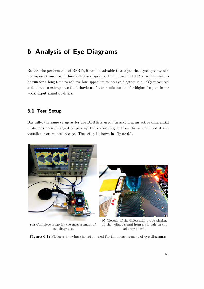
6 Analysis of Eye Diagrams
Besides the performance of BERTs, it can be valuable to analyse the signal quality of ahigh-speed transmission line with eye diagrams. In contrast to BERTs, which need tobe run for a long time to achieve low upper limits, an eye diagram is quickly measuredand allows to extrapolate the behaviour of a transmission line for higher frequencies orworse input signal qualities.
6.1 Test Setup
Basically, the same setup as for the BERTs is used. In addition, an active differentialprobe has been deployed to pick up the voltage signal from the adapter board andvisualize it on an oscilloscope. The setup is shown in Figure 6.1.
(a) Complete setup for the measurement ofeye diagrams.
(b) Closeup of the differential probe pickingup the voltage signal from a via pair on the
adapter board.
Figure 6.1: Pictures showing the setup used for the measurement of eye diagrams.
51
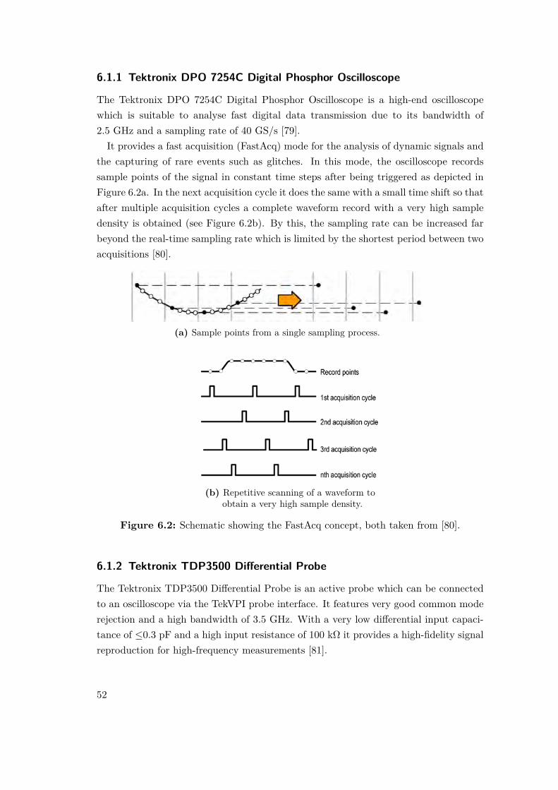
6.1.1 Tektronix DPO 7254C Digital Phosphor Oscilloscope
The Tektronix DPO 7254C Digital Phosphor Oscilloscope is a high-end oscilloscopewhich is suitable to analyse fast digital data transmission due to its bandwidth of2.5 GHz and a sampling rate of 40 GS/s [79].
It provides a fast acquisition (FastAcq) mode for the analysis of dynamic signals andthe capturing of rare events such as glitches. In this mode, the oscilloscope recordssample points of the signal in constant time steps after being triggered as depicted inFigure 6.2a. In the next acquisition cycle it does the same with a small time shift so thatafter multiple acquisition cycles a complete waveform record with a very high sampledensity is obtained (see Figure 6.2b). By this, the sampling rate can be increased farbeyond the real-time sampling rate which is limited by the shortest period between twoacquisitions [80].
(a) Sample points from a single sampling process.
(b) Repetitive scanning of a waveform toobtain a very high sample density.
Figure 6.2: Schematic showing the FastAcq concept, both taken from [80].
6.1.2 Tektronix TDP3500 Differential Probe
The Tektronix TDP3500 Differential Probe is an active probe which can be connectedto an oscilloscope via the TekVPI probe interface. It features very good common moderejection and a high bandwidth of 3.5 GHz. With a very low differential input capaci-tance of ≤0.3 pF and a high input resistance of 100 kΩ it provides a high-fidelity signalreproduction for high-frequency measurements [81].
52

6.2 Eye Diagram Results
In the following, several parameters have been varied and compared to estimate theirinfluence on the signal quality. If multiple eye diagrams are shown side by side, allsettings and in particular the scales are equal unless explicitly stated.
In addition, the signals have been picked up from the same channel (except in 6.2.1)to achieve maximal comparability, i.e. to avoid observing the influence of different tracelengths on the adapter board.
6.2.1 Influence of the HSMC Flexprint Adapter Board
Although the adapter board was designed with a differential impedance of 100 Ω, it islikely to affect the signal quality due to imperfections at its soldering points, i.e. thelocations in which the HSMC connector and the FPC connectors are soldered ontothe PCB. In addition, reflections certainly occur as the differential impedance of theflexprints deviate from 100 Ω.
Comparision of Adapter Board and Loopback Card
Figure 6.3a depicts an eye diagram for data transmission where input and output aredirectly connected via the HSMC loopback card whereas the data transmission via aflexprint is shown in Figure 6.3b.
The comparison reveals that the shape of the signal is changed in some ways. A cleardistinction is visible regarding the eye height which is comprehensible due to ohmiclosses along the flexprint.
In both eye diagrams, one observes two slight dips shortly after a transition. But forthe setup involving the loopback card, there is a strong dip nearly simultaneous withthe next transition whereas the corresponding dip comes a bit later when using theadapter board and a flexprint.
It could be that the dip in Figure 6.3a is caused by reflections on the FPGA develop-ment board. Since the signal is picked up very closely to the HSMC connector in case ofthe loopback card but a few centimeters away on the adapter card, this might introducea difference in the runtime of the reflected signal which leads to the observed shift ofthe dip. Another reason could be crosstalk between adjacent traces on the flexprint.
53

(a) Transmission via loopback card. (b) Transmission via flexprint.
Figure 6.3: Eye diagrams to compare transmission involving the loopback card andthe adapter board. The flexprint has a trace width of 100 µm, a traceseparation of 150 µm between all traces, a Kapton thickness of 50 µm plusaluminum ground plane, and a length of 30 cm.
Comparison of Different Channels
The HSMC Adapter Board is not designed symmetrically and has traces of differentlengths. On the transmitter side, they vary between 38.6 mm and 48.2 mm and on thereceiver side between 26.2 mm and 40.0 mm, respectively.
For the eye diagrams in Figure 6.4, the signal has been picked up at channels 0,11 and 16. Since the traces on the flexprint might slightly differ in trace thicknessor separation due to production tolerances, for the eye diagrams in the right columnthe flexprint has been connected with interchanged ends (see Figure 6.5). I.e. differentchannels have been compared using exactly the same differential pair on the flexprintfor maximal comparability.
It can be seen that interchanging the ends of the flexprint makes only a very slight dif-ference, which could be introduced by an improper connectivity to the FPC connector.On the contrary, there is a strong disparity when comparing the different channels.
For the flexprint used in this comparison it can be assumed that the reflections atthe HSMC connector dominate the total reflections on the receiver side because theseare of first order, whereas reflections caused by an improper impedance matching ofthe flexprint are of second order or higher (see Figure 6.6). Therefore, it is likely thatthe differences between the eye diagrams seen in Figure 6.4 are primarily caused bydifferent runtimes of the reflections due to different trace lengths on the receiver side ofthe PCB and possibly also on the FPGA development board.
54

(a) Channel 0. PCB trace length attransmitter/receiver side: 46.1 mm/26.2 mm.
(b) Channel 0. Flexprint connected withinterchanged ends.
(c) Channel 11. PCB trace length attransmitter/receiver side: 38.7 mm/35.54 mm.
(d) Channel 11. Flexprint connected withinterchanged ends.
(e) Channel 16. PCB trace length attransmitter/receiver side: 40.7 mm/40.0 mm.
(f) Channel 16. Flexprint connected withinterchanged ends.
Figure 6.4: Eye diagrams picked up at different channels. 800 Mbit/s transmissionvia a flexprint with a trace width of 100 µm, a trace separation of 150 µmfor pairs and 650 µm between pairs, and a Kapton thickness of 50 µm plusaluminum ground plane. Length: 10 cm.
55

Figure 6.5: Interchange of the ends of the flexprint for maximal comparability.
Figure 6.6: Schematic of the reflections at the FPC and the HSMC connectors. Γflexcan be calculated with equation 3.4, ΓHSMC is not known.
6.2.2 Influence of the Cable Length
To estimate the influence of the cable length on the signal quality, three flexprints withdifferent lengths are compared in Figure 6.7.
As can be seen, the length does not affect the qualitative shape of the eye. In allcases, there are basically two dips after a transition. This supports the theory that thereflections due to improper impedance matching of the flexprint do not dominate thetotal reflection. In fact, one would expect different signal shapes because of differentruntimes of the reflected signals unless the cable lengths equal multiples of the wave-length. This is unlikely since with a base frequency of 400 MHz and a propagationvelocity of approximately 2/3 of the speed of light, the wavelength should be roughly50 cm.
56

(a) Length: 10 cm. (b) Length: 20 cm.
(c) Length: 30 cm.
Figure 6.7: Eye diagrams of 800 Mbit/s data transmission via flexprints with a tracewidth of 100 µm, a trace separation of 150 µm for pairs and 650 µm betweenpairs, and a Kapton thickness of 50 µm plus aluminum ground plane, butdifferent lengths.
As the signal deformation is independant of the cable length, one can rather proceedon the assumption that reflections at the flexprint are not even visible in these eyediagrams.
However, one observes that there is an attenuation of the signal which grows with thecable length. This meets the expectation since the ohmic resistance of the aluminumtraces rises with their lengths.
In addition, the jitter is enhanced for the longer cables. Nevertheless, the basic eyeshape is conserved and the signal transmission works properly.
57

Figure 6.8: Eye diagram of an 800 Mbit/s data transmission via a flexprint with atrace width and a trace separation of 150 µm, a Kapton thickness of50 µm plus aluminum ground plane, and a length of 50 cm.
Another eye diagram, which is shown in Figure 6.8, has been recorded for a 50 cmflexprint. In contrast to the flexprints discussed above, it had a trace width and a traceseparation of 150 µm.
Compared to the eye diagrams in Figure 6.7 one observes a further decrease of the eyeheight and less distinct dips. This meets the expectations due to higher ohmic lossescaused by the length. Surprisingly, the amout of jitter is reduced towards the 30 cmflexprint in Figure 6.7c, but a reason for this observation could not be found.
58
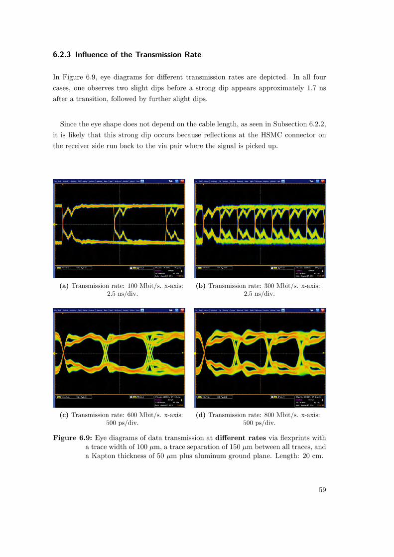
6.2.3 Influence of the Transmission Rate
In Figure 6.9, eye diagrams for different transmission rates are depicted. In all fourcases, one observes two slight dips before a strong dip appears approximately 1.7 nsafter a transition, followed by further slight dips.
Since the eye shape does not depend on the cable length, as seen in Subsection 6.2.2,it is likely that this strong dip occurs because reflections at the HSMC connector onthe receiver side run back to the via pair where the signal is picked up.
(a) Transmission rate: 100 Mbit/s. x-axis:2.5 ns/div.
(b) Transmission rate: 300 Mbit/s. x-axis:2.5 ns/div.
(c) Transmission rate: 600 Mbit/s. x-axis:500 ps/div.
(d) Transmission rate: 800 Mbit/s. x-axis:500 ps/div.
Figure 6.9: Eye diagrams of data transmission at different rates via flexprints witha trace width of 100 µm, a trace separation of 150 µm between all traces, anda Kapton thickness of 50 µm plus aluminum ground plane. Length: 20 cm.
59

The slight dips might come from a limited bandwidth of the transmitter since theyappear independent of the frequency and even when using the loopback card (see Fig-ure 6.3a) so that they are definitely not caused by the flexprint or the adapter board.
Besides, the slew rate is observed to be equal for all frequencies which indicates thatit is limited by the transmitter. Also, the eye height does not change with the frequency.
Even though the frequency could not be increased beyond 800 Mbit/s due to limi-tations of the transmitter, the signal shape allows to assume that the flexprints wouldalso work at higher transmission rates because the deformation of the signal does notshow any frequency dependence and the bit states are always clearly distinguishable.
6.2.4 Influence of the Pre-Emphasis
At high frequencies, the slew rate of the transmitter is not fast enough to reach the fullvoltage level before the next transition. This conduces to a pattern dependent jitterbecause the edge of a transition comes a bit earlier if the full voltage level has not beenreached yet.
To minimize this jitter, the amplitude of the high-frequency components of the out-put signal can be enhanced. This so-called pre-emphasis leads to a voltage overshootshortly after a transition and increases the slew rate [67].
(a) Pre-emphasis disabled. (b) Pre-emphasis enabled.
Figure 6.10: Eye diagrams showing the effect of enabled pre-emphasis. The flexprinthas a trace width of 100 µm, a trace separation of 150 µm between all traces,a Kapton thickness of 25 µm plus aluminum ground plane, and a length of30 cm. Transmission rate: 800 Mbit/s.
60

Figure 6.10 depicts the change in the signal shape due to enabled pre-emphasis. Theovershoot and an increased slew rate are clearly recognisable. Especially in the firstquarter, the eye opening is notably larger. Furthermore, it can be seen that the amountof jitter is reduced.
6.2.5 Crosstalk between Trace Pairs
To examine how much noise is induced on an adjacent trace pair, the firmware wasslightly changed so that only every second channel was used for data transmission andthe intermediate trace pairs were not assigned to FPGA pins.
(a) Signal on channel 0.Kapton thickness: 25 µm, no ground plane.
(b) Induced signal on channel 1.Kapton thickness: 25 µm, no ground plane.
(c) Signal on channel 0.Kapton thickness: 50 µm plus ground plane.
(d) Induced signal on channel 1.Kapton thickness: 50 µm plus ground plane.
Figure 6.11: Eye diagrams showing crosstalk for different Kapton thicknesses. Datatransmission at 800 Mbit/s via flexprints with a trace width of 100 µm, atrace separation of 150 µm between all traces, and a length of 20 cm.
61

For the eye diagrams in the right column of Figure 6.11, the signal was picked up atan unassigned trace pair between two properly working channels. One observes thatcrosstalk is present for both types of flexprints, i.e. for coplanar striplines as well as fordifferential microstrips. But in case of the coplanar striplines, there is a clear periodicstructure in the induced signal whereas for the differential microstrips it is mostly flatand thus interpreted as noise.
Moreover, the amplitude of the induced signal is much larger for the coplanar striplines.This means that the aluminum ground plane really effectively shields the adjacent chan-nels and decreases the amount of crosstalk.
6.2.6 Influence of the Microstrip Type
In Figure 6.12, eye diagrams for different microstrip types can be seen. The comparisonshows that the eye diagrams clearly differ regarding the band thicknesses. The bandsin the signal for the coplanar striplines (Figure 6.12a) are notably widened and alsothe amount of jitter is increased. On the other hand, the two signals for the differ-ential microstrips with different Kapton thicknesses (Figures 6.12b and 6.12c) do notsignificantly deviate from each other.
This is comprehensible when regarding the results from Subsection 6.2.5. In case ofthe coplanar striplines the amount of crosstalk is much larger than for the differentialmicrostrips since the aluminum ground plane effectively shields adjacent trace pairs andminimizes crosstalk.
In contrast, the basis eye shape does not differ. In all three cases, there are twoslight dips after a transition and for those bands remaining at a logic level for longerthan one unit interval, there is another stronger dip somewhat after the next transition.Furthermore, all dips are nearly of equal intensity.
In Subsection 6.2.2, it has been seen that the signal deformation for differentialstriplines on 50 µm Kapton (with ground plane) are not dependent on the length,except for the attenuation of the amplitude. This led to the conclusion that reflectionsdue to improper impedance matching are not observable in the eye diagram.
Since the intensity of the dips does not notably differ for the different microstriptypes, it is likely that the effect of impedance matching is negligible in all three cases.
To support this theory, the runtime of the reflected signals are estimated: The dis-tance, the signal has to run, comprises twice the cable length of 20 cm and a tracelength of 4 mm from the FPC connector to the via pair where the signal is picked up.
62

A propagation velocity of 2/3 of the speed of light and a base frequency of 400 Mbit/sresult in a runtime of approximately 2 ns. But 2 ns after the transition in Figures6.12a-c no specific dip can be observed.
Therefore, it can be concluded that the impedance matching is only of minor impor-tance for the eye shape and crosstalk affects the signal quality much more.
(a) Coplanar Stripline. Kapton thickness:25 µm without ground plane, calculated
Zdiff ≈ 268 Ω.
(b) Differential Microstrip. Kaptonthickness: 25 µm on ground plane, calculated
Zdiff ≈ 40 Ω.
(c) Differential Microstrip. Kaptonthickness: 50 µm on ground plane, calculated
Zdiff ≈ 90 Ω.
Figure 6.12: Eye diagrams of 800 Mbit/s data transmission via flexprints with a tracewidth of 100 µm, a trace separation of 150 µm between all traces, and alength of 20 cm, but different microstrip types.
63

6.2.7 Influence of the Knee Length
For flexprints with a trace separation of 150 µm between all traces, there is a spreadat both ends to meet the 0.5 mm pitch of the FPC connectors. The question ariseswhether the length of the knees (i.e. the sections running 45 to the main section) no-tably impair the signal quality because here the trace thickness and separation deviatefrom the main section and the edges of the traces are less smooth (see Figures 4.5b and4.6b).
To estimate this influence, channels 0, 8 and 16, i.e. the channel with no knee at all,a mean knee length, and the one with the longest knee, are compared in Figure 6.13.Again, the flexprint is connected with interchanged ends in the right column to dis-tinguish the influence of the knee from the intrinsic differences of the channels (seeFigure 6.14).
The eye diagrams for channel 8 should and do look exactly the same in both casessince 8 is in the middle of 17 and the direction of the data transmission should makeno difference due to the symmetric structure of the cable.
Also the other eye diagrams for no knee and the maximal knee length look fine. Thecomparison of Figures 6.13a and 6.13b shows that there is only a very slight differencein the height of the wiggles, whereas the basic signal shape is conserved. The amountof jitter does not notably differ. The same is observed in Figures 6.13e and 6.13f.
Consequently, the influence of the knee length can be considered to be of minorimportance and the use of 45 sections in a flexprint does not significantly impair thesignal quality.
64

(a) No knee (channel 0). (b) Maximal knee length (channel 0).Flexprint connected with interchanged ends.
(c) Medium knee length (channel 8) (d) Medium knee length (channel 8).Flexprint connected with interchanged ends.
(e) Maximal knee length (channel 16). (f) No knee (channel 16). Flexprint connectedwith interchanged ends.
Figure 6.13: Eye diagrams for different knee lengths. 800 Mbit/s transmission viaa flexprint with a trace width of 100 µm, a trace separation of 150 µmbetween all traces, and a Kapton thickness of 50 µm plus aluminum groundplane. Length: 10 cm.
65

Figure 6.14: Interchange of the ends of the flexprint to compare different knee lengthsusing the same channel.
66

Part III
Conclusion & Outlook

7 Conclusion
For this thesis, Kapton flexprints have been produced with a laser system at the Hei-delberg University for the Mu3e experiment. Bit Error Rate Tests (BERTs) at a trans-mission rate of 800 Mbit/s have been performed which resulted in upper limits forthe bit error rates below O(10−15). Furthermore, eye diagrams have been analyzed tounderstand which factors mainly affect the signal quality.
7.1 Manufacturing of Kapton Flexprints
It has been shown that flexprints with a (horizontal) trace width and a trace separationof ≥ 120 µm can be manufactured with a high reliability, i.e. without any broken traces.These can also be combined with 45 sections and vertical sections of traces with a widthof ≥ 150 µm. The vertical sections should rather be short and can be used as pads toconnect the flexprints to the FPC connectors.
Also flexprints with smaller (horizontal) trace widths down to 100 µm can be manu-factured but show broken traces (mostly 1-3 in 34, sometimes more).
With the used laser platform, it is not possible go below a trace separation of 100 µmwhich corresponds to the width of the laser focus. It is problematic to use small traceseparations in a design because the laser changes its mode from ’rastering’ to ’vectoring’for a separation of ≤ 100 µm and an offset or imprecision introduced by the mechanicsof the laser platform leads to inaccurate traces.
This means that the production of flexprints is limited to be done with a single lasersetting for ’rastering’. ’Vectoring’ is only suited to cut out the flexprint.
It has also been shown that differential microstrips can be realized by gluing a flex-print and an unprocessed piece of Kapton laminated with aluminum of the same shapetogether. This can be done with both sides of the Kapton-aluminum foil so that differ-ential microstrips with a Kapton thickness of 25 µm plus adhesive layer or 50 µm plusadhesive layer can be obtained. The influence of different Kapton thicknesses on theimpedance matching and crosstalk was examined and measurements were performed.
68

Possible reasons for the blackening of the Kapton due to the processing with the laserhave been discussed. According to the interpretation given, the laser treatment doesnot significantly change the dielectric properties of the Kapton to the detriment of theexperiment.
7.2 BERT Results
BERTs have been performed that have shown that data transmission works flawlesslyfor a variety of flexprints. Even coplanar striplines without a ground plane can be usedfor an errorless data transmission though the signal quality is worse in comparison todifferential microstrips (see Section 7.3).
7.3 Eye Diagram Results
The analysis of multiple eye diagrams has lead to the following results:
• The signal deformations which can be observed in the eye diagrams are neitherdependent on the transmission rate nor on the flexprint length. The shape evenresembles the signal picked up from the loopback card alone. Therefore, thesignal deformations are unlikely to be caused by reflections at the FPC connectorsdue to improper impedance matching. Consequently, a differential impedancefor flexprints of the type ’differential microstrips’ in the range of 40-60 Ω seemssufficient to minimize the reflections to an acceptable level.
• Comparing flexprints of different lengths has shown that the eye height decreaseswith increasing cable length. Nevertheless, also for 50 cm flexprints, the signalshape allows a clear distinction between the logic states.
• The signal shape looks much better for flexprints of the type ’differential mi-crostrips’ than ’coplanar striplines’. The additional aluminum ground plane de-creases crosstalk effectively and possibly also improves impedance matching. More-over, it provides space for ground and power supply which would have to be placedon the flexprint itself in case of ’coplanar striplines’. Even though it increases thematerial budget, the amount of scattering is notably reduced in comparison toleading-edge flexprints applying copper (see Section 4.3).
• An enabled pre-emphasis enhances the signal quality and increases the slew rate ofthe signal. Nevertheless, also without this option enabled a flawless data transmis-sion is possible at 800 Mbit/s. Although pre-emphasis involves further electronics,
69

namely an additional LVDS driver, which leads to a higher power consumption,this option is foreseen on the final Mupix chip [82].
7.4 Recommendations
In the present work, it could be shown that it is possible to produce Kapton flexprintswith the PLS6MW Multi-Wavelength Laser Platform and transmit data at a rate of800 Mbit/s with a BER below O(10−15) at 95% CL.
A proper trace separation works down to 110 µm and the trace width can be decreaseddown to 100 µm. However, it has been observed that this minimal trace width leadsto broken traces and is therefore not suitable for mass production with the used laserplatform, whereas for trace widths ≥ 120 µm the connectivity is reliable. In addition,it has been seen that a ground (or other constant potential) plane notably improves thesignal quality.
Based on these results, the following recommendations (see also Table 7.1) can bemade:
Since a reliable connectivity of the traces is crucial, a trace width of 120 µm isrecommended. This can be combined with a trace separation of 110 µm. For traceswhich are routed with an angle of 45 to the main section an increased trace width andtrace separation of each 150-175 µm should be used. Also structures perpendicular tothe main direction can be included in the design but should rather be used as pads forthe connection of FPC plugs or the like.
An additional aluminum plane improves the signal quality and delivers more spacefor power supply and ground so that it should be used for the Mu3e experiment eventhough it slightly increases the material budget.
trace width [µm] trace separation [µm]
horizontal 120 11045 ≥ 150 ≥ 150
vertical ≥ 150 ≥ 150
Table 7.1: Recommended structure sizes for the Mu3e experiment.
70

8 Outlook
8.1 Consequences for the Mu3e Experiment
8.1.1 Spatial Constraints
When regarding the spatial constraints of the Mu3e detector, the structure sizes shownin Table 7.1 are sufficient for flexprints to connect the Mupix chips to the front-endFPGAs:
The inner double layer will have a polygonial shape with an active length of 12 cmconsisting of 12 and 18 sides, respectively. Since the final chip size of the Mupix chipswill be 1 × 2 cm2 in the inner region, 6 chips will be used on every side of which 3will be connected upstream and 3 downstream. Each of these chips will have 3 LVDSoutput ports.
Consequently, 9 parallel LVDS channels need to be placed on one flexprint. A tracewidth of 120 µm and a trace separation of 110 µm lead to a total width of 0.414 cmfor the horizontal section. Since each chip has a length of 2 cm, there will be an areaof 0.586× 2 cm2 to spread the traces using 45 sections and place bonding pads.
Ground and power could be supplied by integrating holes in the Kapton to be ableto bond on the underlying ground/power plane as depicted in Figure 8.1. For thispurpose, differential microstrips on 25 µm Kapton would be much easier to producethan on 50 µm because in case of the latter, one would need to find a way to partiallyremove the Kapton from the aluminum to bond to the underlying metal plane.
These structure sizes also suffice for the outer polygonials which will have a lengthof 36 cm and 24-26 sides with a width of 2 cm. Here, the chips will have a size of2 × 2 cm2 so that 18 chips will be mounted in a row. These will have only 1-2 LVDSoutput channels so that to each side ≤18 channels need to be placed on a 2 cm wideflexprint. This is at most as narrow as in the inner layers and should work as well [10].
71

Figure 8.1: Schematic showing the concept of bonding on the underlying aluminumplane.
8.1.2 Transmission Errors
In phase I of the Mu3e experiment, 180 chips with 3 LVDS output channels each willbe used in the innermost double layer. The outer double layer will mount 972 chipswith 1-2 channels each so that the total number of channels adds up to ≤ 2142 [10].
With a BER ≤ 10−15 at 95% CL and equation 3.12 the mean time τ for an error tooccur can be estimated:
BER = # errors# total bits
!= 1800 Mbit/s ·# channels · τ (8.1)
⇒ τ ≥ 86 min. (8.2)
Note that the ”true” value for τ might be much larger because no error bit has beenobserved.
Since the pixel detectors will be read out in time frames of 50 ns (see Subsection 2.1.3),this means that only a very small fraction of ≤ 10−11 of the readout frames will containan error bit (if at all) whereas it is very unlikely that two error bits occur in the sameframe. The firmware or software should be able to detect a single error bit so that suchan unemployable readout frame can be discarded. Due to the very low rate of framescontaining error, this would not harm the experiment.
72

8.2 Further Work
Several tasks are left which must be focused on in subsequent works. These are:
• The flexprints which have been produced so far did only act as test cables to showthat data transmission at 800 Mbit/s works in principle and to find out suitabletrace widths and trace separations which can be manufactured reliably.
Further investigations have to be done on flexprint designs which really fit theMupix chips and the spatial constraints in the detector.
• It has been seen, that an aluminum ground plane notably increases the signalquality since it suppresses crosstalk between adjacent trace pairs and (presumably)also enhances impedance matching.
Still, it has the drawback of an increased material budget which leads to strongermultiple scattering. It should be tested whether a thinner aluminum thickness of< 12 µm can function as a ground (or power) plane.
• Research has to be done on the question how to bond the Mupix chips to theKapton flexprints.
• So far, no statement could be made about the lifetime of the Kapton flexprints.The aluminum might possibly suffer from oxidation which could decrease theconductivity to the FPC connectors or make it more vulnerable to bending sincealuminum oxide is a brittle material.
73

List of Figures
1.1 Particles described by the SM . . . . . . . . . . . . . . . . . . . . . . . . 31.2 Feynman diagrams of possible SM muon decays . . . . . . . . . . . . . . 41.3 Feynman diagrams of possible BMS muon decays . . . . . . . . . . . . . 41.4 The history of LFV muon decay experiments . . . . . . . . . . . . . . . 5
2.1 The internal conversion decay µ+ → e+e−e+νµνe . . . . . . . . . . . . . 72.2 Branching ratio for the internal conversion as a function of the missing
energy . . . . . . . . . . . . . . . . . . . . . . . . . . . . . . . . . . . . . 72.3 Possible combinatorial background . . . . . . . . . . . . . . . . . . . . . 82.4 Schematic drawing of the detector design . . . . . . . . . . . . . . . . . 92.5 First mechanical prototype of the Kapton support structure for the inner
two layers . . . . . . . . . . . . . . . . . . . . . . . . . . . . . . . . . . . 102.6 Schematic of the Mu3e readout chain . . . . . . . . . . . . . . . . . . . . 12
3.1 Basic LVDS circuit . . . . . . . . . . . . . . . . . . . . . . . . . . . . . . 143.2 Binary datastream and corresponding voltage . . . . . . . . . . . . . . 153.3 Two commonly used line codes . . . . . . . . . . . . . . . . . . . . . . . 163.4 Equivalent circuit diagram of a short piece of a transmission line . . . . 183.5 Profiles of differential microstrips and coplanar striplines . . . . . . . . . 203.6 An ideal and a real arbitrary digital datastream and their eye diagrams 233.7 A typical eye diagram with key parameters . . . . . . . . . . . . . . . . 24
4.1 PLS6MW Laser Platform . . . . . . . . . . . . . . . . . . . . . . . . . . 264.2 Dependence of the dielectric constant εr on various quantities . . . . . . 284.3 Test structures to examine which minimal structure sizes can be achieved
by rastering . . . . . . . . . . . . . . . . . . . . . . . . . . . . . . . . . . 334.4 Flexprint type 1 . . . . . . . . . . . . . . . . . . . . . . . . . . . . . . . 344.5 Flexprint type 2 . . . . . . . . . . . . . . . . . . . . . . . . . . . . . . . 354.6 Flexprint type 3 . . . . . . . . . . . . . . . . . . . . . . . . . . . . . . . 364.7 Attempt to cut a single trace into two thin traces . . . . . . . . . . . . . 374.8 Photo showing the thickened ends of two flexprints . . . . . . . . . . . . 384.9 Microscopic images of flexprints showing the blackening of the processed
Kapton . . . . . . . . . . . . . . . . . . . . . . . . . . . . . . . . . . . . 40
5.1 Picture showing the setup comprising the FPGA development board, theHSMC adapter board and the self-manufactured flexprint . . . . . . . . 42
5.2 Stratix V GX FPGA Development Board . . . . . . . . . . . . . . . . . 445.3 HSMC Flexprint Adapter Board . . . . . . . . . . . . . . . . . . . . . . 445.4 Altera HSMC loopback board . . . . . . . . . . . . . . . . . . . . . . . . 45
74

5.5 Schematic of the BERT implementation . . . . . . . . . . . . . . . . . . 465.6 Schematic of the functionality of the data checker . . . . . . . . . . . . . 48
6.1 Pictures showing the setup used for the measurement of eye diagrams . 516.2 Schematics showing the FastAcq concept . . . . . . . . . . . . . . . . . . 526.3 Eye diagrams to compare the transmission involving the loopback card
and the adapter board . . . . . . . . . . . . . . . . . . . . . . . . . . . . 546.4 Eye diagrams picked up at different channels . . . . . . . . . . . . . . . 556.5 Interchange of the ends of the flexprint for maximal comparability . . . 566.6 Schematic of the reflections at the FPC and the HSMC connectors . . . 566.7 Eye diagrams for different cable lengths . . . . . . . . . . . . . . . . . . 576.8 Eye diagram for a 50 cm long flexprint . . . . . . . . . . . . . . . . . . . 586.9 Eye diagrams at different transmission rates . . . . . . . . . . . . . . . . 596.10 Eye diagrams showing the effect of enabled pre-emphasis . . . . . . . . . 606.11 Eye diagrams showing crosstalk for different Kapton thicknesses . . . . 616.12 Eye diagrams for Kapton thicknesses . . . . . . . . . . . . . . . . . . . . 636.13 Eye diagrams for different knee lengths . . . . . . . . . . . . . . . . . . . 656.14 Interchange of the ends of the flexprint to compare different knee lengths
using the same channel . . . . . . . . . . . . . . . . . . . . . . . . . . . . 66
8.1 Schematic showing the concept of bonding on the underlying aluminumplane . . . . . . . . . . . . . . . . . . . . . . . . . . . . . . . . . . . . . . 72
75

List of Tables
3.1 5b/6b encoding . . . . . . . . . . . . . . . . . . . . . . . . . . . . . . . . 173.2 3b/4b encoding . . . . . . . . . . . . . . . . . . . . . . . . . . . . . . . . 183.3 Typical parameters for microstrips on PCBs and flexprints . . . . . . . . 21
4.1 Some physical properties of aluminum and copper . . . . . . . . . . . . 294.2 Calculation of the impedance for coplanar striplines on 25 µm Kapton . 304.3 Calculation of the impedance for differential microstrips on 25 µm Kapton 304.4 Calculation of the impedance for differential microstrips on 50 µm Kapton 304.5 Laser settings used to produce test patterns and flexprints . . . . . . . . 314.6 Laser settings used to produce test patterns and flexprints . . . . . . . . 32
5.1 Start values of the data generators . . . . . . . . . . . . . . . . . . . . . 475.2 Example for an error being counted twice . . . . . . . . . . . . . . . . . 495.3 BERT results for various coplanar striplines . . . . . . . . . . . . . . . . 505.4 BERT results for various differential microstrips on 25 µm Kapton . . . 505.5 BERT results for differential microstrips on 50 µm . . . . . . . . . . . . 50
7.1 Recommended structures sizes for the Mu3e experiment . . . . . . . . . 70
76

Bibliography
[1] J. Beringer et al., [Particle Data Group], “Review of Particle Physics (RPP)”,Phys.Rev., D86 010001, 2012.
[2] G. Aad et al., [ATLAS Collaboration], “Observation of a new particle in the searchfor the Standard Model Higgs boson with the ATLAS detector at the LHC”, Hyper-fine Interact., 214(1-3) 5–11, 2012, (arXiv:1207.7214 [hep-ex]).
[3] S. Chatrchyan et al., [CMS Collaboration], “Observation of a new boson at amass of 125 GeV with the CMS experiment at the LHC”, Phys.Lett.B, 2012,(arXiv:1207.7235 [hep-ex]).
[4] Wikimedia Commons, Standard Model of Elementary Particles, http://en.wikipedia.org/wiki/File:Standard_Model_of_Elementary_Particles.svg,2014, [Online; accessed 10-Februar-2014].
[5] Y. Fukuda et al., [Super-Kamiokande Collaboration], “Evidence for Oscil-lation of Atmospheric Neutrinos”, Phys. Rev. Lett., 81 1562–1567, 1998,(arXiv:hep-ex/9807003).
[6] Q. R. Ahmad et al., [SNO Collaboration], “Measurement of the charged currentinteractions produced by B-8 solar neutrinos at the Sudbury Neutrino Observatory”,Phys. Rev. Lett., 87 071301, 2001, (arXiv:nucl-ex/0106015).
[7] K. Eguchi et al., [KamLAND Collaboration], “First results from KamLAND: Evi-dence for reactor anti- neutrino disappearance”, Phys. Rev. Lett., 90 021802, 2003,(arXiv:hep-ex/0212021).
[8] F.P. An et al., [Daya Bay Collaboration], “Observation of electron-antineutrino dis-appearance at Daya Bay”, Phys.Rev.Lett., 108 171803, 2012, (arXiv:1203.1669[hep-ex]).
[9] L. Canetti and M. Shaposhnikov, “The ν MSM and muon to electron conversionexperiments”, Hyperfine Interact., DOI: 10.1007/s10751-013-0796-7, 2013.
[10] A. Blondel et al., “Research Proposal for an Experiment to Search for the De-cay µ → eee”, ArXiv e-prints 1301.6113, January 2013, (arXiv:1301.6113[physics.ins-det]).
[11] W. J. Marciano, T. Mori and J. M. Roney, “Charged Lepton Flavor ViolationExperiments”, Ann.Rev.Nucl.Part.Sci., 58 315–341, 2008.
[12] Y. Kuno and Y. Okada, “Muon Decay and Physics Beyond the Standard Model”,Rev. Mod. Phys., 73 151–202, 2001, (arXiv:hep-ph/9909265).
77
[13] D. Nicolo, [MEG Collaboration], “The µ → eγ experiment at PSI”,Nucl.Instrum.Meth., A503 287–289, 2003.
[14] U. Bellgardt et al., [SINDRUM Collaboration], “Search for the Decay µ+ →e+e+e−”, Nucl.Phys., B299 1, 1988.
[15] J. Adam et al., [MEG Collaboration], “New Constraint on the Existence of theµ+ → e+γ Decay”, Phys. Rev. Lett., 110 201801, May 2013.
[16] A.M. Baldini et al., “MEG Upgrade Proposal”, ArXiv e-prints, January 2013,(arXiv:1301.7225 [physics.ins-det]).
[17] A. Blondel et al., Letter of intent for an experiment to search for the decay µ→ eee,2012.
[18] M. Kiehn, Track Fitting with Broken Lines for the MU3E Experiment, Diplomathesis, Heidelberg University, 2012.
[19] R. M. Djilkibaev and R. V. Konoplich, “Rare Muon Decay µ+ → e+e−e+νeνµ”,Phys.Rev., D79 073004, 2009, (arXiv:0812.1355 [hep-ph]).
[20] I. Peric et al., “High-voltage pixel detectors in commercial CMOS technologies forATLAS, CLIC and Mu3e experiments”, Nucl.Instrum.Meth., A731 131–136, 2013.
[21] N. Berger et al., “A Tracker for the Mu3e Experiment based on High-VoltageMonolithic Active Pixel Sensors”, Nucl. Instr. Meth. A, 732 61–65, 2013,(arXiv:1309.7896 [physics.ins-det]).
[22] H. Augustin, Charakterisierung von HV-MAPS, Bachelor thesis, Heidelberg Uni-versity, 2012.
[23] A.-K. Perrevoort, Characterisation of High Voltage Monolithic Active Pixel Sensorsfor the Mu3e Experiment, Master thesis, Heidelberg University, 2012.
[24] R. Philipp, Characterisation of High Voltage Monolithic Active Pixel Sensors forthe Mu3e Experiment, Master thesis, Heidelberg University, 2014.
[25] C. Grzesik, Fast Optical Readout for the Mu3e Experiment, Bachelor thesis, Hei-delberg University, 2014.
[26] S. Corrodi, Fast Optical Readout of the Mu3e Pixel Detector, Master thesis, Hei-delberg University, ETH Zurich, 2014.
[27] S. Bachmann et al., The proposed trigger-less TBit/s readout for the Mu3e exper-iment, In JINST 9 C01011 doi:10.1088/1748-0221/9/01/C01011, 2014.
[28] A. Damyanova, Development of a Scintillating Fibre Tracker/Time-of-Flight De-tector with SiPM Readout for the Mu3e Experiment at PSI, Master’s thesis, GenevaUniversity, 2013.
[29] P. Eckert, In Preparation, PhD thesis, Kirchhoff Institut fur Physik, 2015.
78

[30] M. Zimmermann, Cooling with Gaseous Helium for the Mu3e Experiment, Bachelorthesis, Heidelberg University, 2012.
[31] L. Huxold, Cooling of the Mu3e Pixel Detector, Bachelor thesis, Heidelberg Uni-versity, 2012.
[32] A. Herkert, In Preparation, Master thesis, Heidelberg University, 2015.
[33] G.S. Bauer, Y. Dai and W. Wagner, “SINQ layout, operation, applications andR&D to high power”, J. Phys. IV France, 12(8) 3–26, 2002.
[34] A. P. Clark, Principle of Digital Data Transmission. Wiley, 1983.
[35] G. Cariolaro, Unified signal theory. London : Springer, 2011.
[36] M. Werner, Signale und Systeme, volume 3. Vieweg+Teubner, 2008.
[37] H. Zimmermann, “OSI Reference Model - The ISO Model of Architecture for OpenSystems Interconnection”, IEEE Transactions on Communications, 28(4) 425–432,1980.
[38] Wikimedia Commons, Low-Voltage Differential Signaling, http://en.wikipedia.org/wiki/LVDS, 2014, [Online; accessed 12-August-2014].
[39] http://www.maximintegrated.com/en/app-notes/index.mvp/id/3662, Under-standing LVDS Fail-Safe Circuits, 2014, [Online; accessed 11-August-2014].
[40] M. Pauer, Return-to-zero Coding in Optical Intersatellite Links. Technische Uni-versitat Wien, 2003.
[41] Wikimedia Commons, Leitungscode, http://de.wikipedia.org/wiki/Leitungscode, 2014, [Online; accessed 12-August-2014].
[42] R. Forster, “Manchester encoding: Opposing definitions resolved”, Engineering Sci-ence & Education Journal, 2000.
[43] D. Derickson and M. Muller, Digital Communications Test and Measurement:High-Speed Physical Layer Characterization. Prentice Hall, December 2007.
[44] A. X. Widmer and P. A. Franaszek, “A DC-Balanced, Partitioned-Block, 8B/10BTransmission Code”, IBM Journal of Research and Development, 27(5) 440, 1983.
[45] Wikimedia Commons, Ersatzschaltbild eines kurzen Stuckes einer Zweidraht-leitung, http://de.wikipedia.org/wiki/Leitungstheorie#mediaviewer/Datei:Leitungsbelag.svg, 2014, [Online; accessed 11-August-2014].
[46] M. Johnson and W. Graham, High-Speed Signal Propagation. Prentice Hall PTR,2003.
[47] E. Bogatin, Training for signal integrity and interconnect design, http://www.ewh.ieee.org/r5/denver/rockymountainemc/archive/2000/diffimp.pdf, 2000.
79

[48] D. Brooks, “Differential Impedance - What’s the Difference?”, Printed Circuit De-sign, 1998.
[49] P. Vielhauer, Theorie der Ubertragung auf elektrischen Leitungen. Verlag Technik,1970.
[50] D. Brooks, Printed Circuit Board Design. Prentice Hall PTR, 2003.
[51] S. Gevorgian and H. Berg, “Line Capacitance and Impedance of Coplanar-StripWaveguides on Substrate with Multiple Dielectric Layers”, IEEE Xplore, year un-known.
[52] Wurth Elektronik, Basic Design Guide, 2012, http://www.wedirekt.de/web/live/media/16_wedirekt/spezifikationen/leiterplatten_daten_downloads/WEdirektBasicDesignGuide.pdf.
[53] Dyconex, Design Guide 2013 (External), 2013, Available on request via e-mail.
[54] T. Hebbeker, “Calculating Upper Limits with Poisson Statistics”, http://web.physik.rwth-aachen.de/˜hebbeker/l3note-2633.pdf, 2001.
[55] I. Narsky, “Estimation of Upper Limits Using a Poisson Statistic”, arXiv:hep-ex/9904025, page 24, 1999.
[56] ON Semiconductor, “Understanding Data Eye Diagram Methodology for AnalysingHigh Speed Digital Signals”, Semiconductor Components Industries, LLC,AND9075/D, 2014.
[57] http://uniquelaserengravers.tradeindia.com/pl6mw-1118929.html, [On-line; accessed 20-August-2014].
[58] Universal Laser Systems, PLS User Guide, 2012.
[59] DuPont, Kapton R© HN polyimide film - Technical Data Sheet, 2011.
[60] DuPont, Kapton R© HN - Summary of Properties, year unknown.
[61] M. Bauccio, ASM Metals Reference Book. ASM International, 1993.
[62] http://www.aluinfo.de/index.php/aluminium-in-electrical-engineering-and-electronics.html, [Online; accessed 20-August-2014].
[63] Los Alamos National Laboratory, http://periodic.lanl.gov/13.shtml, [On-line; accessed 20-August-2014].
[64] S. Eidelman et al., “Passage of Particles Through Matter”, Physics Letters B592,2004.
[65] J. Bartl and M. Baranek, “Emissivity of Aluminum and its Importance for Radio-metric Measurements”, Measurement Science Review, 2004.
[66] Y. Kaburagi and Y. Hishiyama, “Ferromagnetism discovered on heat-treating thearomatic polyimide film Kapton”, J. Mater. Res., 2002.
80

[67] Altera, Stratix V Device Handbook, 2013.
[68] W. Rogers et al., FPGA-based Implementation of Signal Processing Systems. Wiley,2008.
[69] Altera, Stratix V Device Overview, 2014.
[70] Altera, Stratix V GX FPGA Development Board - Reference Manual, 2014.
[71] http://www.altera.com/products/devkits/altera/kit-sv-gx-host.html,[Online; accessed 21-August-2014].
[72] Altera, High Speed Mezzanine Card (HSMC) - Specification, 2009.
[73] Altera, Quartus II Handbook Volume 1: Design and Synthesis, 2014.
[74] V. A. Pedroni, Circuit Design with VHDL. MIT Press, 2004.
[75] S. Palnitkar, Verilog HDL: A Guide to Digital Design and Synthesis. Prentice HallPTR, 2003.
[76] ModelSim SE, User’s Manual, 2002.
[77] Ken Boyette, http://read.pudn.com/downloads104/sourcecode/embed/425959/8b_10b/8b10_enc.vhd__.htm, 2006, [Online; accessed 25-April-2014].
[78] Ken Boyette, http://read.pudn.com/downloads104/sourcecode/embed/425959/8b_10b/8b10_dec.vhd__.htm, 2006, [Online; accessed 25-April-2014].
[79] Tektronix, Digital-Phosphor-Oszilloskope - DPO7000C-Serie Datenblatt, 2013.
[80] Altera, DPO7000 Series - Digital Phosphor Oscilloscopes - Quick Start User Man-ual.
[81] Tektronix, Differential Probes - TDP1500 and TDP3500 Datasheet, 2013.
[82] I. Peric, Personal Contact, September 2014.
81

82

Acknowledgements
At the end of my thesis, I would like to thank everyone who supported me to carry outthis thesis.
First of all, I would like to express my appreciation to Prof. Dr. Andre Schoningwho gave me the opportunity to work in the Mu3e group. He helped me especially bycritically questioning my strategies and supposing new approaches.
I would also like to thank Prof. Dr. Ulrich Uwer for being my second examiner.
Moreover, I would like to express my gratitude to the following persons in nospecific order:
• Carsten Grzesik, with whom I have spent much time in the lab and at the laserplatform. I also profited a lot from his experience.
• Qinhua Huang, who taught me much about VHDL and supported me on FPGAprogramming.
• Dirk Wiedner, who gave me valuable of support on technical and electronicissues and helped me to design my HSMC Flexprint Adapter Board.
• Niklaus Berger, who is an expert in FPGA programming and was able to solveevery problem Qinhua and I were facing.
• Ann-Kathrin Perrevoort and all the others who were always there to answerquestions, proof-read my thesis with great commitment and gave a lot of sugges-tions.
• Finally, the whole Mu3e group for providing a very pleasant and cordial workatmosphere and sharing a time full of new experiences.
83


Erklarung
Ich versichere, dass ich diese Arbeit selbststandig verfasst und keine anderen als dieangegebenen Quellen und Hilfsmittel benutzt habe.
Heidelberg, den 15.09.2014