deposition of ceramic and hybrid materials - material matters v1n3
TRANSCRIPT

8/14/2019 Deposition of Ceramic and Hybrid Materials - Material Matters v1n3
http://slidepdf.com/reader/full/deposition-of-ceramic-and-hybrid-materials-material-matters-v1n3 1/20
2006VOLUME 1NUMBER 3
sigma-aldrich.com
Indispensable in Space and on Earth
– ceramic flms in action.
Chemical DepositionTechniques in MaterialsDesign
Savannah ALD Sstem
Sol-Gel Science forCeramic Materials
Hermetic Barrier UsingVinl Triethoxsilane(VTEOS)
Silicon-Based Passiveand Sstem-in-PackageIntegration
Vacuum Deposited NonPrecious Metal Catalsts
for PEM Fuel Cells
TM
Deposition o Ceramic and Hybrid Materials
8/14/2019 Deposition of Ceramic and Hybrid Materials - Material Matters v1n3
http://slidepdf.com/reader/full/deposition-of-ceramic-and-hybrid-materials-material-matters-v1n3 2/20
s i g
m
a - a l d r i c h
. c o m
Vol. 1 No. 3
Aldrich Chemical Co., Inc.Sigma-Aldrich Corporation6000 N. Teutonia Ave.Milwaukee, WI 53209, USA
To Place Orders
Telephne 800-325-3010(USA)FAX 800-325-5052(USA)
Customer & Technical Services
CustmerInquiries 800-325-3010TechnicalService 800-231-8327SAFC™ 800-244-1173
CustmSnthesis 800-244-1173Flavrs&Fragrances 800-227-4563Internatinal 414-438-385024-HurEmergenc 414-438-3850WebSite sigma-aldrich.cmEmail [email protected]
Subscriptions
TrequesturFREEsubscriptintMaterial Matters,pleasecntactusb:
Phne: 800-325-3010(USA)
Mail: Attn: Marketing Communications
Aldrich Chemical Co., Inc.Sigma-Aldrich Corporation
P.O. Box 355
Milwaukee, WI 53201-9358
Email: [email protected]
Internatinal custmers, please cntact lcal Sigma-Aldrich fce. Fr wrldwide cntinrmatin,pleaseseebaccver.
Material MattersisalsavailableinPDFrmattheInternetatsigma-aldrich.com/matsci.
Aldrich brand prducts are sld thrugh SigmAldrich, Inc. Sigma-Aldrich, Inc. warrants thatprducts cnrm t the inrmatin cntainedthisandtherSigma-Aldrichpublicatins.Purchasmustdeterminethesuitabilittheprductrparticularuse.Seereversesideinvicerpacislipradditinaltermsandcnditinssale.
Allpricesaresubjecttchangewithutntice.
Material Matters isa publicatinAldrich ChemC., Inc.Aldrich is a member the Sigma-AldGrup.©2006Sigma-AldrichC.
TM
I n t r o d u
c t i o n
About Our Cover
The need or ilms and coatings is ubiquitous in the technological age we live. For example, ilms servingas humidity barriers orm an essential part o microelectronics, micro-electromechanical systems andenergy conversion devices. The cover depicts a molecule o vinyl triethoxysilane (VTEOS) that could beused to make a barrier ilm by chemical deposition. VTEOS is a multiunctional molecule that enables thegeneration o a hybrid silicon oxide ilm with polymerizable vinyl groups; the inorganic content is designedto be the barrier, while the hydrophobic, organic content repels water and ills porosity; or more details,please reer to the article by the Rutgers research group on page 11. As alluded to on the cover, such a
ilm could be used to seal the elements o solar panels on a geosynchronous satellite or protection romthe external environment.
Introduction
Welcome to the third issue o Material MattersTM. This issue ocuses on chemicaldeposition techniques and their application in electronics and alternative energy.
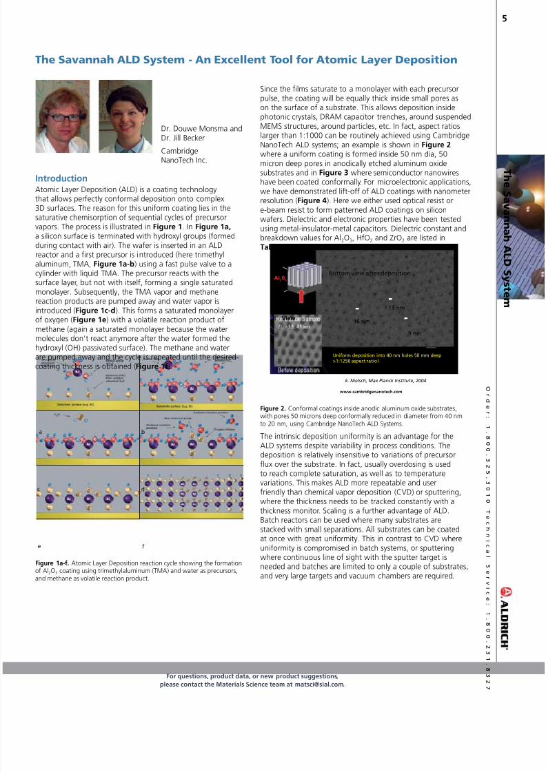
An introduction and comparison o chemical vapor deposition and solution depositionapproaches to ilm abrication is given by Dr. Balema o Sigma-AldrichTM MaterialsScience. Scientists rom Cambridge NanoTech discuss Chemical Vapor Deposition(CVD) and Atomic Layer Deposition (ALD), as well as advantages o the Savannah
ALD system. Dr. Young rom the US Army Research Laboratory highlights basics osol-gel science or ceramic materials. The group o Pro. Klein rom Rutgers Universitypresents a paper on the development o a hermetic barrier using vinyl triethoxysilane(VTEOS) via Sol-Gel Processing. Dr. Roozeboom rom Philips and Pro. Kessels romthe University o Technology, Eindhoven, Netherlands, discuss the suitability o atomiclayer deposition in the abrication o Si-based integrated passives and System-in-Package integration. Finally, researchers rom the 3M Company led by Dr. Atanasoskiand Dr. O’Neill report on the use o vacuum deposition in the preparation o electrodematerials or uel cells. Products that accelerate your research in the undamental andapplied science o chemical deposition are highlighted. We invite your comments,questions and suggestions about Material MattersTM and materials o interest to you:[email protected].
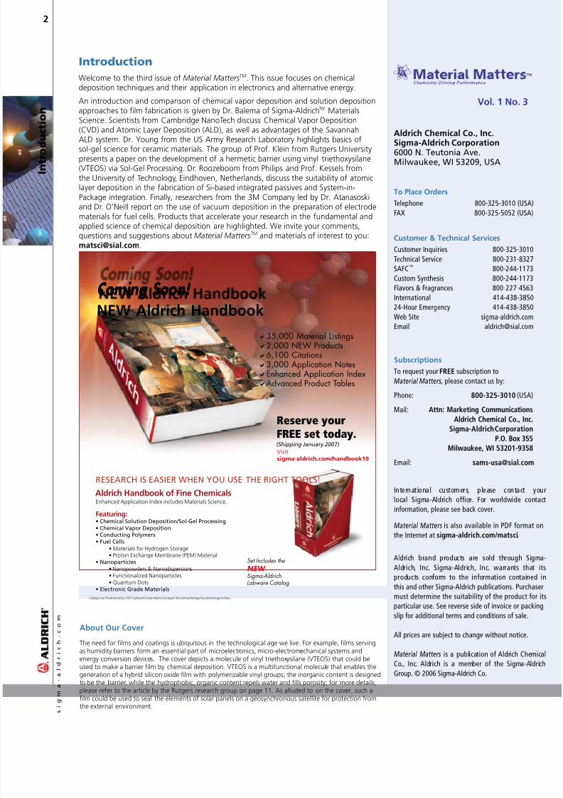
Coming Soon!
Reserve yourFREE set today.
NEW Aldrich Handbook
RESEARCH IS EASIER WHEN yOU USE THE RIGHT TOOLS!
Visit sigma-aldrich.com/handbook19
Catalog Cover:The Alchemist (ca.1937) by Newell Convers Wyeth.Courtesy of the Chemical Heritage Foundation Image Archives.
Aldrich Handbook of Fine Chemicals
Set Includes the NEW
Sigma-AldrichLabware Catalog
Featuring: • Chemical Solution Deposition/Sol-Gel Processing• Chemical Vapor Deposition• Conducting Polmers• Fuel Cells
• Materials or Hydrogen Storage• Proton Exchange Membrane (PEM) Material
• Nanoparticles • Nanopowders & Nanodispersions• Functionalized Nanoparticles• Quantum Dots
• Electronic Grade Materials
Enhanced Application Index includes Materials Science.
35,000 Material Listings2,000 NEW Products6,100 Citations3,000 Application NotesEnhanced Application IndexAdvanced Product Tables
(Sppn Januay 2007)
8/14/2019 Deposition of Ceramic and Hybrid Materials - Material Matters v1n3
http://slidepdf.com/reader/full/deposition-of-ceramic-and-hybrid-materials-material-matters-v1n3 3/20
For questions, product data, or new product suggestions,please contact the Materials Science team at [email protected].
O
r d
er :
1
. 8
0
0
. 3
2
5
. 3
0
1
0
T e
c h
n
i c a
l
S e
r vi c e
:
1
. 8
0
0
.2
3
1
. 8
3 2
7
3
Ch emi c al D e p o si ti on
T e c h ni q u e s
Materials with a layer thickness below 1 µm are calledthin ilms, while thicker layers, especially those exceedingdimensions o a transistor in an electronic chip, are deinedas thick ilms. Both thin and thick ilms play an exceptionallyimportant role as elements o electronic and optical devices,
computer memory chips, and in other related applications.Additionally, in the case o ceramic ilms, properties such aschemical resistivity and hardness enable their use as coatingson substrate materials and cutting tools or protection againstcorrosion, oxidation, and wear.
Typically, CVD/ALD techniques are methods o choice orthe deposition o thin ilms on inorganic substrates, whilesolution-based sol-gel approaches are considered when thickilms or nano-powders are desired. Also, lower equipmentcost and reasonably good conormality o coatings may makesol-gel a low-cost alternative to CVD/ALD. However, the ALDapproach may be required or the preparation o uniormconormal ilms on complex suraces such as those with highaspect ratios.
Usually, the nature o the deposition process determines theway in which the thickness o the ilm is controlled. Thus, inconventional CVD, the ilm growth depends on the depositiontime, while in ALD it is controlled by the number o depositioncycles.1-3 In sol-gel processing, the ilms are created using twomajor approaches – spin coating or dip coating. In the irstcase, the substrate is spun at an angular speed ω and theprecursor (sol) is directed onto its surace along the rotationaxis. The thickness (h) o the created ilms depends on acomplex combination o the sol’s properties and the rotationspeed o the substrate. In practice, they can be predictedusing a semi-empirical ormula
h = Aω Β
where A and B are empirical coeicients. The dip coatingprocess consists o the successive dipping and withdrawal othe substrate in and out o the solution. The thickness o theilm obtained in one dipping-withdrawal cycle is determined8 by the properties o the solution, i.e. viscosity (η), density (ρ),surace tension (σ) and the withdrawal speed ( n) :
h = 0.945{( nη)2/3 / (gρ)1/2σ1/6}
While CVD/ALD techniques produce thin ilms o highuniormity and metal purity, sol-gel processing provides aunique and simple approach to tuning the ilm’s chemicalcomposition and morphology. Sol-gel processing can also oera less expensive alternative to CVD/ALD, especially i in situdoping is required.
An example, when solution processing has been used
successully as an alternative to CVD/ALD was in thepreparation o silicon thin-ilm transistors where thedeposition o a polycrystalline silicon used a liquid precursor,cyclopentasilane (Si5H10).
9 The grain size in the ilms obtainedwere ound to be as low as 300 nm, comparable to that orilms typically prepared by CVD.
Dr. Viktor P. Balema
Sigma-Aldrich Materials Science
During the last decade, chemical deposition techniques haveplayed an exceptionally important role in the design andmanuacture o novel advanced devices. Physical depositiontechniques, such as molecular beam epitaxy (MBE), physicalvapor deposition (PVD) or sputtering, have been used orthese applications. However, they suer rom limitations suchas poor conormality, low throughput, restricted directionalvariation, and reduced compositional control. All o theseissues can and have been addressed using chemical depositiontechniques which oer additional advantages such as ultra-thin ilm growth. This is especially the case when layered
inorganic materials are assembled in order to create anelectronic chip or to modiy the surace o a tool or improvedperormance and durability. Currently, two groups o dierent,yet related, techniques dominate the ield. The irst groupcomprising Chemical Vapor Deposition (CVD) and AtomicLayer Deposition (ALD) uses a gas phase to transport volatilemolecules to the surace serving as a substrate. The secondgroup o deposition techniques, called Chemical SolutionDeposition or Sol-Gel Processing, uses a liquid phase as themass transer media.
There is a undamental resemblance between these twogroups - the way that the inal material is created. In bothcases, molecules o chemical compounds serving as precursorsare delivered to the substrate surace and chemically modiied
to obtain the desired ilm. It should be noted, however, thatthe chemical transormations o the precursor in the caseo CVD/ALD can occur in the gas phase and at the gas-solid interace, while in sol-gel processing it is carried out insolution (Figure 1). In the CVD/ALD approach, the chemicalmodiication o the precursor is usually achieved via thermalconversion o precursor molecules and/or their reactions withmolecules o other volatile precursors, or reactive gases suchas oxygen or hydrogen.1-3 Sol-gel processing consists o asequence o chemical transormations in solution and solid-state. They include ormation o a colloidal suspension in anappropriate solvent (sol), gelation (gel), evaporation o thesolvent (drying), and thermal treatment (sintering). 4-7
Sol
Gel
Xerogel
Film
Precursor(s)
ALDCVD
ALD
ALD
CVD
CVD
Sintering
Drying
Gelation
Chemical Deposition
Solution Vacuum
Figure 1. Schematic illustrating chemical deposition o ceramic ilms.
Chemical Deposition Techniques in Materials Design

8/14/2019 Deposition of Ceramic and Hybrid Materials - Material Matters v1n3
http://slidepdf.com/reader/full/deposition-of-ceramic-and-hybrid-materials-material-matters-v1n3 4/20
TO ORDER: Contact your local Sigma-Aldrich office (see back cover),call 1-800-35-3010 (USA), or visit sigma-aldrich.com/matsci.
s i g
m
a - a l d r i c h
. c o m
C h e m i c a l D e p o s i t i o n
T e c h n i q u e s
An illustration where CVD is clearly preerred over solvent-based processing, is the deposition o magnesium aluminumspinel (MgAl2O4). Magnesium aluminum spinel is an excellentmaterial or reractory applications because o its mechanicalstrength, chemical resistance, and low density. Also, it showspotential as a humidity sensor and as a buer layer or thegrowth o oxide superconductors. Thin ilms o MgAl2O4 havebeen successully prepared by CVD using Mg-Al precursors
such as MgAl2(OPr-i)8 or MgAl2(OBu-t)8. Sol-gel processingwas employed or this application using a similar intermediate,MgAl2[(OCH2CH2)N]3, resulting in micro-porous powders.10,11 Remarkably, certain groups o precursors, such as metalalkoxides, or example, can be used successully in both CVD/ ALD and Chemical Solution Deposition/Sol-Gel Processing ometal-oxide ilms and nano-structures.12-14
Thus, when used to the best o their abilities, Chemical Vaporand Solution Deposition techniques are excellent tools, toenable the design o a broad range o materials with pre-deined dimensions, morphology and properties.
Acknowledgements I would like to thank Dr. S. Jasty, Dr.A.Korolev, Dr. M. Stender,and S. Adam or discussions and help in the preparation o the
manuscript.
References:(1) D.M. Dobkin and M.K. Zuraw, Principles of Chemical Vapor Deposition: What’s Going on Inside the Reactor , 003, KluwerAcademic Publishers, Boston, Dodrecht, London. (2) R. Fischer,Precursor Chemistry of Advanced Materials, 005, Springer, NewYork. (3) D. Monsma, J. Becker, Material Matters, 006, Vol. 1,No. 3, 5. (4) S.K.Young’s, Material Matters, 006, Vol 1., No. 3, 8.(5) F. Caruso, Colloids and Colloid Assemblies: Synthesis,Modification, Organization, and Utilization of Colloid Particles,
00, John Wiley & Sons, New York. (6) Sol-Gel Technology for Thin Films, Fibers, Preforms, Electronics, and Specialty Shapes, L.C.Klein, Ed., 1988, Noyes Publ., Park Ridge, NJ.(7) A.C.Pierre, Introduction to Sol-Gel Processing, 00 KulwerAcademic Publishers, Boston, Dodrecht, London. (8) V. Kiisk,Optical Investigation of Metal-Oxide Films, 006, Tartu UniversityPress, Tartu. (9) T. Shimoda, Y. Matsuki, M. Furusawa, T. Aoki,I. Yudasaka, H. Tanaka, H. Iwasawa, D. Wang, M. Miyasaka, Y.Takeuchi, Nature, 006, 440, 783. (10) K.F.Waldner, R.M.Laine,S. Dhumrongvaraporn, S.Tayaniphan, R.Narayanan, Chem. Mater .1996, 8, 2850 (11) S.Mathur, M.Veith, T.Ruegamer, E.Hemmer,H.Shen, Chem. Mater . 00, 16, 1304. (12) N. Lecer, S. Mathur,H. Shen, M. Veith, S. Huener, Scripta Mater . 001, 44, 2157(13) M. Veith, J. Chem. Soc., Dalton Trans., 00, 2405 (14) L.G.Hubert-Palzgra, Inorg. Chem. Communications 003, 6, 102.
High-Purity Metal Alkoxides
Metal Precursor Linear Formula Purity (%) Product No.
Aluminum Aluminum isopropoxide Al[OCH(CH3)2]3 99.99 907-10G
907-50G
907-50G
Aluminum-tri-sec-butoxide Al[OCH(CH3)C2H5]3 99.99 511609-5G
Germanium Germanium(IV) ethoxide Ge(OC2H5)4 99.95 339180-1G
339180-5G
339180-5G
Hafnium Hanium(IV) n-butoxide 99 66793-5G
Tetrakis(1-methoxy-2-methyl-2 propoxy)hanium(IV) H(OC(CH3)2CH2OCH3)4 99.99 568171-10G568171-5G
Magnesium Magnesium ethoxide Mg(OC2H5)2 98 9186-5G
9186-100G
Niobium Niobium(V) ethoxide Nb(OCH2CH3)5 99.95 3390-5G
3390-50G
Tin Tin(IV) tert -butoxide Sn(OC(CH3)3)4 99.99 9135-5G
9135-5G
Tantalum Tantalum(V) ethoxide Ta(OC2H5)5 99.98 339113-10G
339113-100G
Titanum Titanium(IV) isopropoxide Ti[OCH(CH3)2]4 99.999 377996-5ML
377996-5ML
377996-100MLTitanium(IV) methoxide Ti(OCH3)4 99.99 6358-5G
Tungsten Tungsten(VI) ethoxide 99 667935-G
667935-10G
Zirconium Zirconium(IV) diisopropoxidebis(2,2,6,6-tetramethyl-3,5-
heptanedionate)
Zr(OCC(CH3)3CHCOC-
(CH3)3)2(OC3H7)2
99.99 9151-5G
9151-5G
Zirconium(IV) isopropoxide isopropanol complex Zr(OCH(CH3)2)4 ·(CH3)2CHOH
99.9 33937-10G33937-50G
Zirconium(IV) tert -butoxide electronic grade Zr[OC(CH3)3]4 99.999 560030-5G
560030-5G
8/14/2019 Deposition of Ceramic and Hybrid Materials - Material Matters v1n3
http://slidepdf.com/reader/full/deposition-of-ceramic-and-hybrid-materials-material-matters-v1n3 5/20
8/14/2019 Deposition of Ceramic and Hybrid Materials - Material Matters v1n3
http://slidepdf.com/reader/full/deposition-of-ceramic-and-hybrid-materials-material-matters-v1n3 6/20
8/14/2019 Deposition of Ceramic and Hybrid Materials - Material Matters v1n3
http://slidepdf.com/reader/full/deposition-of-ceramic-and-hybrid-materials-material-matters-v1n3 7/20
For questions, product data, or new product suggestions,please contact the Materials Science team at [email protected].
O
r d
er :
1
. 8
0
0
. 3
2
5
. 3
0
1
0
T e
c h
n
i c a
l
S e
r vi c e
:
1
. 8
0
0
.2
3
1
. 8
3 2
7
7
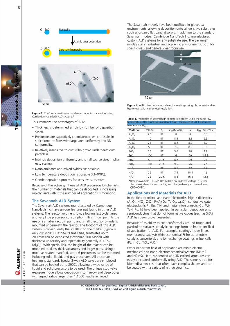
T h e S av ann ah AL D S y s t em
In the ield o optics, large improvements in uniormity ooptical parameters and thickness can be obtained by usingALD. In addition, substrates don’t need to be rotated to becoated all over and batch processes can be applied to reducecost. Several ields o optics beneit rom ALD: nanophotonics,solar cells, integrated optics, lasers, variable dielectric constantnanolaminates, Fabry-Perot, Rugate, lip-lop optical ilters,and anti-relection coatings (Al2O3, ZnS, SnO2, Ta2O5, AlTiO,
SnO2, ZnO). For photonic crystals and inverted opals, ALD isconveniently the only technique that can be used to internalcoatings.
ALD is commercially used in the abrication o magneticread heads (or insulating layers, mainly Al2O3) as well as orlat panel displays. More recently, ALD has proven to createexcellent humidity barriers or organic light emitting displays(OLEDs).
Several niche applications have been ound as well, such aspiezoelectric layers (ZnO, AlN, ZnS), transparent electricalconductors (ZnO:Al, ITO) and gas/pH sensors (SnO2, Ta2O5),wear, solid lubricant and corrosion inhibiting layers (Al2O3,ZrO2, WS2).
Besides many ceramics, ALD can now also deposit variousmetals, such as Ru, Pd, Ir, Pt, Rh, Co, Cu, Fe, and Ni,increasing the number o applications and advancing science
by allowing precision coatings in places where no othertechnique has gone beore.
References: (1) K. Nielsch, Max Planck Institute, Germany, privatecommunication. (2) Hongjin Fan, Nature Materials online, July006, 1. (3) Biercuk et al. Appl. Phys. Lett. 003, 83, 2405.
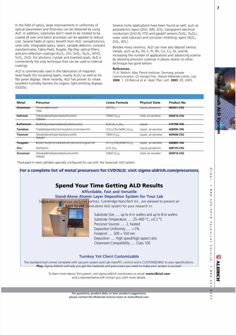
Volatile Precursors for Savannah ALD System*
Metal Precursor Linear Formula Physical State Product No.
Aluminum TrimethylaluminumTMA
Al(CH3)3 Liquid, pyrophoric 663301-5G
Hafnium Tetrakis(dimethylamido)hanium(IV)TDMAH H[N(CH3)2]4 Solid, air-sensitive 666610-5G
Ruthenium Bis(Ethylcyclopentadienyl)ruthenium(LI) Ru(C5H4-C2H5)2 Liquid 679798-10G
Tantalum Tris(diethylamido)( tert -butylimido)-tantalum(V) (CH3)3CN=Ta(N(C2H5)2)3 Liquid, air-sensitive 668990-10G
Titanium Tetrakis(dimethylamido)titanium(IV)TDMAT
Ti[N(CH3)2]4 Liquid, air-sensitive 669008-5G
Tungsten Bis(tert -butylimino)bis(dimethylamino)tungsten(VI) ((CH3)3CN)2W(N(CH3)2)2 Liquid, air-sensitive 668885-10G
Zinc Diethylzinc Zn(C2H5)2 Liquid, pyrophoric 66879-5G
Zirconium Tetrakis(dimethylamido)zirconium(IV)TDMAZ
Zr[N(CH3)2]4 Solid, air-sensitive 669016-5G
*Packaged in steel cylinders specially conigured or use with the Savannah ALD system.
For a complete list of metal precursors for CVD/ALD, visit sigma-aldrich.com/precursors.
Spend Your Time Getting ALD Results
Affordable, Fast and VersatileStand-Alone Atomic Layer Deposition System for Your Lab
Sigma-Aldrich and our exclusive partner, Cambridge NanoTech Inc., are pleased to present an
EASY TO USE stand-alone ALD system or your research in:
Turnkey Yet Client Customizable
The standard tool comes complete with vacuum system and Lab-View/PC control and is CUSTOMIZABLE to your specifcations.Plus, Sigma-Aldrich will help you get the materials and precursors you need to make your project a success!
To learn more about this system, visit sigma-aldrich.com/matsci or email [email protected] a representative will contact you with more details.
Substrate Size ..... up to 4-in wafers and up to 8-in wafersSubstrate Temperature ..... 25–400 °C; ±0.2 °CPrecursor Sources .... . 2, heatedDeposition Uniformity ..... <1%
Footprint ..... 500 × 550 mmDeposition ..... High speed/high aspect ratioCleanroom Compatibility ..... Class 100
8/14/2019 Deposition of Ceramic and Hybrid Materials - Material Matters v1n3
http://slidepdf.com/reader/full/deposition-of-ceramic-and-hybrid-materials-material-matters-v1n3 8/20
8/14/2019 Deposition of Ceramic and Hybrid Materials - Material Matters v1n3
http://slidepdf.com/reader/full/deposition-of-ceramic-and-hybrid-materials-material-matters-v1n3 9/20
For questions, product data, or new product suggestions,please contact the Materials Science team at [email protected].
O
r d
er :
1
. 8
0
0
. 3
2
5
. 3
0
1
0
T e
c h
n
i c a
l
S e
r vi c e
:
1
. 8
0
0
.2
3
1
. 8
3 2
7
9
S ol - G el S ci e
n c ef or
C er ami c M a
t er i al s
Modifing the Sol-Gel NetworkA convenient way to modiy ceramic and composite materials,such as those reerred to in the previous paragraph isthrough the use o Organically Modiied Silicates (ORMOSILs).ORMOSILs are derived rom tetraunctional silicon alkoxidessuch as TEOS, as shown in Figure , where n is representativeo the number o organic moieties connected to the siliconatom and f is representative o the number o reactive
alkoxy groups connected to the silicon. R, R’, and R” are theunctional group(s) on an organically modiied silicate such asmethyl, vinyl, or benzyl. Oten, the organic moiety includesa reactive group such as an amine or epoxide, which makespossible subsequent reactions.
OCH2CH
3
R'
OCH2CH
3SiR
OCH2CH
3
R'
R"SiR
OCH2CH 3
OCH2CH
3
OCH2CH
3SiR
OCH2CH 3
OCH2CH
3
OCH2CH
3SiH
3CH
2CO
Terminating Bridging
Endcapping Network Forming
f=1,n=3 f=2, n=2
f=3, n=1 f=4, n=0
Figure . Functionality o ORMOSILs
Silsesquioxanes are other widely used inorganic-organicmodiiers in ceramic and composite materials. Bridgingsilsesquioxanes (Figure 3) contain a substituent (R) thatis hydrocarbon based but can also contain organic spacerunctionalities. Since silsesquioxanes are oten incorporatedinto polymer systems, the R-group should be as similaras possible to the repeat unit thus increasing interacecompatibility.
SiR"
H3CH
2CO
H3CH
2CO
R"
OCH2CH
3
OCH2CH
3
R SiSiH3CH
2CO
H3CH
2CO
H3CH
2CO
OCH2CH
3
OCH2CH
3
OCH2CH
3
R Si
Figure 3. Examples o a 6-arm and a 4-arm Bridging Silsesquioxane.
In addition, numerous caged structures are beingincorporated into ceramic and composite materials throughsol-gel chemistries. These structures, such as polyhedralsilsesquioxanes19,20 (also commonly known as PSS) or zeolites,21 add speciic porosity and rigidity to the material. Cagedstructures can be incorporated through non-covalent (trappingthe material within the ceramic structure) or covalent bonding.
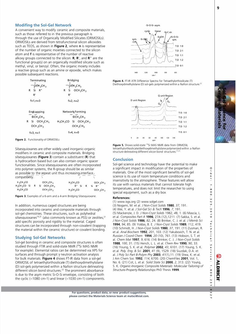
Studying Sol-Gel NetworksSol-gel bonding in ceramic and composite structures is otenstudied through FTIR and solid-state NMR (29Si MAS NMRor example). Elemental ratios can be determined via XPS orsuraces and through prompt γ neutron activation analysisor bulk materials. Figure shows FT-IR data rom a sol-gelORMOSIL o tetraethylorthosilicate (T):diethoxydimethylsilane(D) sol-gels polymerized within a Naion structure delineatingdierent silicon bond structures.22 The prominent absorbanceis due to the asym metric Si-O-Si envelope, consisting o boththe cyclic (~1080 cm-1) and linear (~1030 cm-1) components.
1400 1200 1000 800 600
cm-1
sym.-CH 3
-Si-OEt
-Si-O-Si- asym.
cyclic linear
-Si-OH
-Si-C str.
-Si-O-Si-sym.
T:D 1:0
T:D 2:1
T:D 1:1
T:D 1:2
T:D 0:1
Figure . FT-IR ATR Dierence Spectra or Tetraethylorthosilicate (T):Diethoxydimethylsilane (D) sol-gels polymerized within a Naion structure.22
0 - 20 - 40 - 60 - 80 -100 -120 -140
ppm
T:D 1:0
T:D 2:1
T:D 1:1
T:D 1:2
T:D 0:1
D unit Region
Q unit Region
D2
Q4Q3
Figure 5. Shows solid-state 29Si MAS NMR data rom ORMOSILtetraethylorthosilicate/diethoxydimethylsilane polymerized within a Naionstructure delineating dierent silicon bond structures.17,21
ConclusionSol-gel science and technology have the potential to makea signiicant impact in modiication o the properties omaterials. One o the most signiicant beneits o sol-gel
science is its use o room temperature conditions andinsensitivity to the atmosphere. These eatures will allowits use with various materials that cannot tolerate hightemperatures, and does not limit the researcher to usingspecial equipment, such as a dry box.
References:(1) www.isgs.org (2) www.solgel.com(3) Nogami, M. et al. J Non-Cryst Solids 1980, 37 , 191.(4) Wei, Y. et al. J Sol-Gel Sci & Tech 1996, 7 , 191.(5) Mackenzie, J. D. J Non-Cryst Solids 1982, 48, 1. (6) Mascia, L.et al. Composites Part A 1996, 27A (12),1211. (7) Sakka, S. et al.
J Non-Cryst Solids 1986, 82, 24. (8) Brinker, C. J. et al. J Memb Sci 199, 94, 85. (9) Yoldas, B. E. J Non-Cryst Solids 1989, 112, 419.(10) Schmidt, H. J Non-Cryst Solids 1980, 37 , 191. (11) Zusman, R.et al. Anal Biochem 199, 201, 103. (12) Yakubovich, T. N. et al.Russian J Coord Chem 199, 20 (10), 761. (13) Hobson, S. T. etal. Chem Mat 1997, 9, 616. (14) Brinker, C. J. J Non-Cryst Solids 1988, 100, 31. (15) Hench, L. L. et al. Chem Rev 1990, 90, 33.(16) Young, S. K. et al. Polymer 00, 43, 6101. (17) Young, S. K.et al. Poly. Eng. & Sci. 001, 41 (9), 1529. (18) Siuzdak, D.A. etal. J Poly Sci Part B-Polym Phy 003, 41(1),11. (19) Shea, K. et al.J Am Chem Soc 199, 114, 6700. (20) ChemFiles 001, Vol. 1,No. 6. (21) Cot, L. et al. Solid State Sci 000, 2, 313. (22) Young,S. K. Organic-Inorganic Composite Materials: Molecular Tailoring of Structure-Property Relationships PhD Thesis 1999.
8/14/2019 Deposition of Ceramic and Hybrid Materials - Material Matters v1n3
http://slidepdf.com/reader/full/deposition-of-ceramic-and-hybrid-materials-material-matters-v1n3 10/20
TO ORDER: Contact your local Sigma-Aldrich office (see back cover),call 1-800-35-3010 (USA), or visit sigma-aldrich.com/matsci.
s i g
m
a - a l d r i c h
. c o m
10
S o l - G e
l S c i e n c e f o r
C e r a m
i c M a t e r i a l s
Tri(methoxy)silanes H3CO Si
OCH3
OCH3
R
CH3
0175 (95%)
CH3
CH2
3563 (>97%)
CH
CH2
35758 (98%) 107 (98%)
CH2
3830 (98%)
CF3CH2
91877 (97%)
OCH2
1331 (98%)
CH2 Cl
0183 (>97%)
CH2 Br
1865 (97%)
CH2 SH
175617 (95%)
CH2 NH2
81778 (97%)
CH2 HN CH3
551635 (97%)
CH2 HN
NH2
O
0817 (97%)
CH2 HN
NH2
1088 (97%)
HNCH2
0809 (97%)
CH2 N H2C
CH3
Si
OCH3
OCH3
OCH3
555150 (97%)
CH2 O
O
0167 (98%)
CH2 O
CH3
H2C
O
0159 (98%)
CH2(CH2)6CH3
3761 (96%)
CH2(CH2)14CH3
5360 (>85%)
CH2(CH2)16CH3
37613 (90%)
Tri(ethoxy)Silanes H3CH2CO Si
OCH2CH3
OCH2CH3
R
CH2
CH2
3910 (96%)
CH2
CH3
539317 (97%)CH2
CH3
H3C
35678 (98%)
CH2 96 (>97%)
CH2
CH2
A36301 (97%)
CH2
CN
15377 (97%)
CH2(CH2)3CH3
10160 (>97%)Cl
CH2
35686 (95%)
CH2 NH2
010 (99%)
CNCH2
37156 (98%)
CH2(CH2)6CH3
013 (>96%)
CH2CH2CF2(CF2)4CF3
6670 (98%)
CH2CH2CF2(CF2)6CF3
658758 (97%)
CH2(CH2)10CH3
37 (>95%)
Other Alkoxysilanes
H3C Si
CH3
OCH3
CH3
53006 (99%)
H3C Si
CH3
OCH2CH3
CH3
5371 (98%)
Si
CH3
OCH2CH3
OCH2CH3H3C
175595 (97%)
H3C Si
OCH3
OCH3
603 (97%)
H3CH2CO Si
OCH2CH3
CH3
CH2
596 (99%)
Si
OCH2CH3
8319 (97%)
H3C Si
OCH3
OCH3
CH2(CH2)6CH3
6815 (>95%)
H3C Si
CH3
OCH3
CH2(CH2)6CH3
375977 (98%)
Si
OCH2CH3
OCH2CH3
CH2(CH2)16CH3H3C
5793 (95%)
H3CH2CO Si
OCH2CH3
CH3
NH2
371890 (97%)
H2CH3CO Si
CH3
OCH2CH3
O O
35171 (97%)
H2CH3CO Si
CH3
CH3
O O
53960 (97%)
H3CO Si
CH3
OCH3
SH
6173 (95%)
H3CH2CO Si
OCH2CH3
D8353 (97%)
Silane Precursors
For unit sizes and prices o products below, please visit sigma-aldrich.com.
8/14/2019 Deposition of Ceramic and Hybrid Materials - Material Matters v1n3
http://slidepdf.com/reader/full/deposition-of-ceramic-and-hybrid-materials-material-matters-v1n3 11/20
8/14/2019 Deposition of Ceramic and Hybrid Materials - Material Matters v1n3
http://slidepdf.com/reader/full/deposition-of-ceramic-and-hybrid-materials-material-matters-v1n3 12/20
TO ORDER: Contact your local Sigma-Aldrich office (see back cover),call 1-800-35-3010 (USA), or visit sigma-aldrich.com/matsci.
s i g
m
a - a l d r i c h
. c o m
1
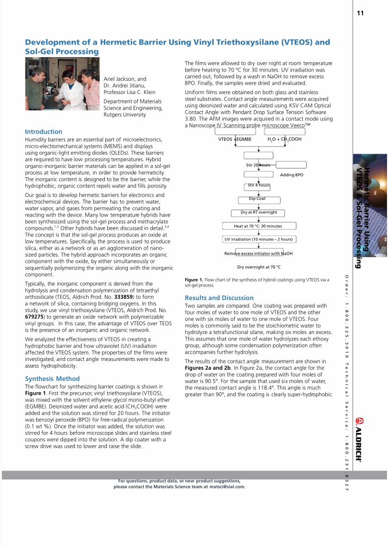
Figure a. Contact angle u, or coating prepared using our molesH2O: u = 90.5°.
Figure b. Contact angle u, or coating prepared using six molesH2O: u = 118.4°.
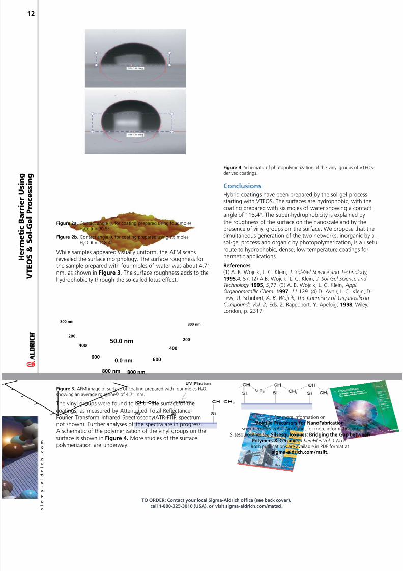
While samples appeared visually uniorm, the AFM scansrevealed the surace morphology. The surace roughness orthe sample prepared with our moles o water was about 4.71nm, as shown in Figure 3. The surace roughness adds to thehydrophobicity through the so-called lotus eect.
800 nm
200
400
600600
400
200
800 nm
800 nm 800 nm
0.0 nm
50.0 nm
Figure 3. AFM image o surace o coating prepared with our moles H2O,showing an average roughness o 4.71 nm.
The vinyl groups were ound to be on the surace o thecoatings, as measured by Attenuated Total Relectance-Fourier Transorm Inrared Spectroscopy(ATR-FTIR spectrumnot shown). Further analyses o the spectra are in progress.A schematic o the polymerization o the vinyl groups on thesurace is shown in Figure . More studies o the suracepolymerization are underway.
H e r m e t i c B a r r i e r
U s i n g
V T E O S & S o l - G e l P r o c
e s s i n g
Figure . Schematic o photopolymerization o the vinyl groups o VTEOS-derived coatings.
ConclusionsHybrid coatings have been prepared by the sol-gel process
starting with VTEOS. The suraces are hydrophobic, with thecoating prepared with six moles o water showing a contactangle o 118.4º. The super-hydrophobicity is explained bythe roughness o the surace on the nanoscale and by thepresence o vinyl groups on the surace. We propose that thesimultaneous generation o the two networks, inorganic by asol-gel process and organic by photopolymerization, is a useulroute to hydrophobic, dense, low temperature coatings orhermetic applications.
References (1) A. B. Wojcik, L. C. Klein, J. Sol-Gel Science and Technology, 1995,4, 57. (2) A.B. Wojcik, L. C. Klein, J. Sol-Gel Science and Technology 1995, 5,77. (3) A. B. Wojcik, L. C. Klein, Appl.Organometallic Chem. 1997, 11,129. (4) D. Avnir, L. C. Klein, D.
Levy, U. Schubert, A. B. Wojcik, The Chemistry of OrganosiliconCompounds Vol. 2, Eds. Z. Rappoport, Y. Apeloig, 1998, Wiley,London, p. 2317.
For more information onVolatile Precursors for NanoFabrication
see ChemFiles Vol 4. No 3 and, for more information onSilsesquioxanes see Silsesquioxanes: Bridging the Gap between
Polymers & Ceramics ChemFiles Vol. 1 No 6.Both publications are available in PDF format at
sigma-aldrich.com/mslit.

8/14/2019 Deposition of Ceramic and Hybrid Materials - Material Matters v1n3
http://slidepdf.com/reader/full/deposition-of-ceramic-and-hybrid-materials-material-matters-v1n3 13/20
For questions, product data, or new product suggestions,please contact the Materials Science team at [email protected].
O
r d
er :
1
. 8
0
0
. 3
2
5
. 3
0
1
0
T e
c h
n
i c a
l
S e
r vi c e
:
1
. 8
0
0
.2
3
1
. 8
3 2
7
13
Deposition Grade Silanes for Sol-Gel Processing
Silane Precursor Structure Product No.
Allyltrimethoxysilane
SiH3CO
OCH3
OCH3
CH2
67967-50G
Butyltrichlorosilane Cl3Si CH3 679-50G
[3-(Diethylamino)propyl]trimethoxysilaneSi
OCH3
OCH3
H3CON
CH3
CH3 679356-50G
Ethyltrichlorosilane CH3Cl3Si 67916-50G
Isobutyl(trimethoxy)silane CH3Cl3Si 67936-50G
Methyltrichlorosilane CH3Cl3Si 67908-50G
N -PropyltriethoxysilaneH3CH2CO Si
OCH2CH3
OCH2CH3
CH3
67931-50G
Pentyltrichlorosilane Cl3Si CH3 67919-50G
Tetramethyl orthosilicate
H3CO Si
OCH3
OCH3
OCH3
67959-50G
Tetrapropyl orthosilicateH3CH2CH2CO Si
OCH2CH2CH3
OCH2CH2CH3
OCH2CH2CH3
6790-50G
Triethoxy(octyl)silaneH3CH2O Si
OCH2CH3
OH2CH3
CH3
679305-50G
TriethoxyphenylsilaneH3CH2CO Si
OCH2CH3
OCH2CH3
67991-50G
TriethoxyvinylsilaneH3CH2CO Si
OCH2CH3
OCH2CH3
CH2
67975-50G
Trimethoxymethylsilane
H3CO Si
OCH3
OCH3
CH3
6793-50G
Trimethoxyphenylsilane
SiH3CO
OCH3
OCH3
679313-50G
Purity o the above deposition-grade silanes is 98+% by chemical assay. Trace metals and impurity proiles are reported on the Certiicate o Analysis.
For a complete list of precursors for Sol-Gel Processing, visit sigma-aldrich.com/solgel.
H er m
e t i c B ar r i er U s i n g
VT E O
S & S ol - G el P r o c e s s i n g
8/14/2019 Deposition of Ceramic and Hybrid Materials - Material Matters v1n3
http://slidepdf.com/reader/full/deposition-of-ceramic-and-hybrid-materials-material-matters-v1n3 14/20
8/14/2019 Deposition of Ceramic and Hybrid Materials - Material Matters v1n3
http://slidepdf.com/reader/full/deposition-of-ceramic-and-hybrid-materials-material-matters-v1n3 15/20
For questions, product data, or new product suggestions,please contact the Materials Science team at [email protected].
O
r d
er :
1
. 8
0
0
. 3
2
5
. 3
0
1
0
T e
c h
n
i c a
l
S e
r vi c e
:
1
. 8
0
0
.2
3
1
. 8
3 2
7
15
Sili c on-B a s e dP a s siv e an d
S y s t em-i n-P a c k a g e
For the deposition o conductive layers by ALD, or theapplication as electrodes, seed layers, diusion barriers (e.g.against Cu-diusion in vias) there is a substantial choicebetween thermal and plasma-assisted ALD. The plasma-based process can lead to improved material properties ashas clearly been demonstrated by results on conductive TiNilms.8 The process based on TiCl4 dosing in combinationwith H2-N2 plasma exposure has yielded thin TiN ilms with
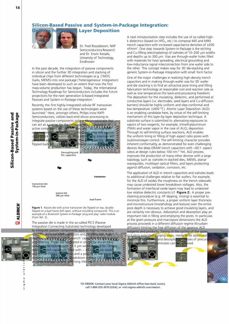
excellent resistivity and low impurity levels (C, H, Cl, etc.)greatly surpassing the material quality achieved with thethermal process employing NH3 dosing. Moreover, in termso acceptable material quality, the thermal process is limitedto the substrate temperature range o 300–400 °C while theplasma-based process can yield air material properties downto temperatures as low as 100 °C.
M
I
S
polySi
Al2O3 /HfO2 /Al2O3
a b
interfacial SiO2
poly-Si
Al2O
3
HfO2
Al2O
3
SiO2
Si-substrate
0.5 µm 10 nm
Figure . (a) SEM cross-section and (b) high-resolution TEM image o anAl2O3 /HO2 /Al2O3 dielectric layer stack, grown by thermal ALD with apoly-Si electrode layer on top.
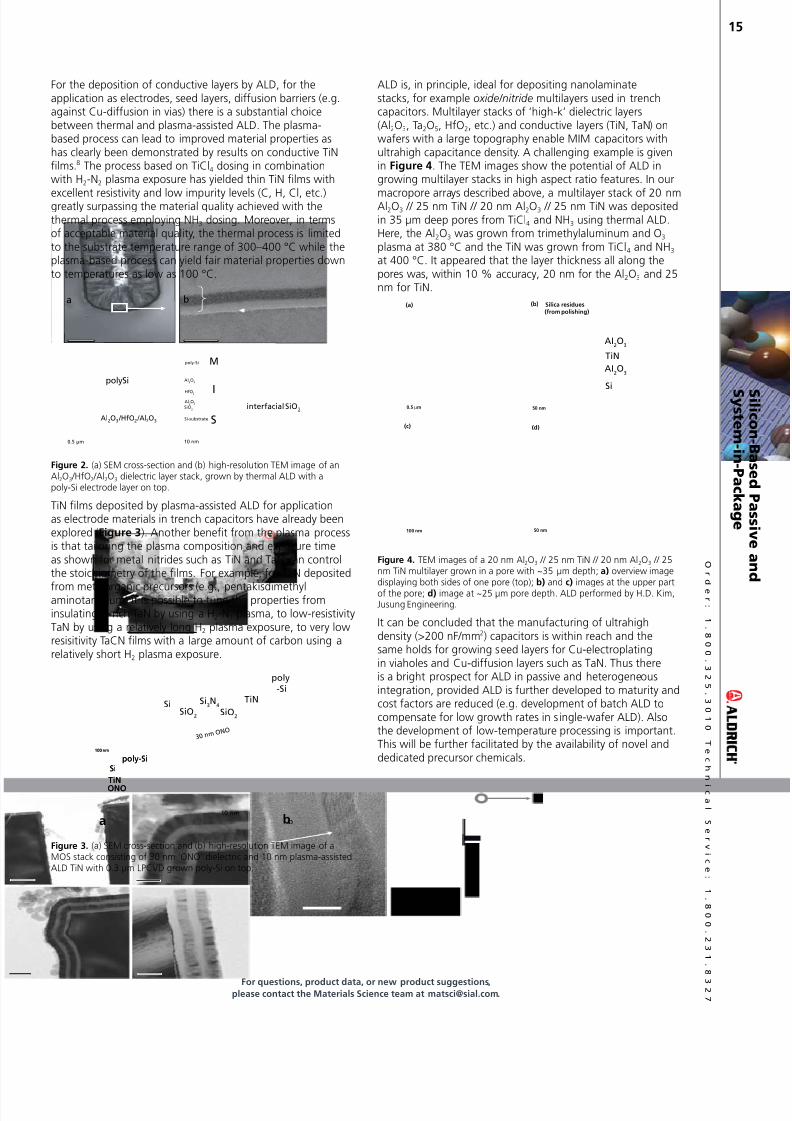
TiN ilms deposited by plasma-assisted ALD or applicationas electrode materials in trench capacitors have already beenexplored (Figure 3). Another beneit rom the plasma processis that tailoring the plasma composition and exposure timeas shown or metal nitrides such as TiN and TaN can controlthe stoichiometry o the ilms. For example, or TaN deposited
rom metalorganic precursors (e.g., pentakisdimethylaminotantalum) it is possible to tune the properties rominsulating N-rich TaN by using a H2-N2 plasma, to low-resistivityTaN by using a relatively long H2 plasma exposure, to very lowresisitivity TaCN ilms with a large amount o carbon using arelatively short H2 plasma exposure.
100 nm
TiNONO
Sipoly-Si
100 nm
TiNONO
Sipoly-Si
b
SiSiO
2
Si3N
4
SiO2
TiN
poly-Si
10 nm
3 0 n m O N
O
a b
Figure 3. (a) SEM cross-section and (b) high-resolution TEM image o aMOS stack consisting o 30 nm ‘ONO’ dielectric and 10 nm plasma-assistedALD TiN with 0.3 µm LPCVD grown poly-Si on top.
ALD is, in principle, ideal or depositing nanolaminatestacks, or example oxide/nitride multilayers used in trenchcapacitors. Multilayer stacks o ‘high-k’ dielectric layers(Al2O3, Ta2O5, HO2, etc.) and conductive layers (TiN, TaN) onwaers with a large topography enable MIM capacitors withultrahigh capacitance density. A challenging example is givenin Figure . The TEM images show the potential o ALD ingrowing multilayer stacks in high aspect ratio eatures. In our
macropore arrays described above, a multilayer stack o 20 nmAl2O3 // 25 nm TiN // 20 nm Al2O3 // 25 nm TiN was depositedin 35 µm deep pores rom TiCl4 and NH3 using thermal ALD.Here, the Al2O3 was grown rom trimethylaluminum and O3 plasma at 380 °C and the TiN was grown rom TiCl4 and NH3 at 400 °C. It appeared that the layer thickness all along thepores was, within 10 % accuracy, 20 nm or the Al2O3 and 25nm or TiN.
AI2O
3
TiN
AI2O
3
Si
Silica residues(from polishing)
(a) (b)
(c) (d)
100 nm
0.5 µm 50 nm
50 nm
Figure . TEM images o a 20 nm Al2O3 // 25 nm TiN // 20 nm Al2O3 // 25nm TiN multilayer grown in a pore with ~35 µm depth; a) overview imagedisplaying both sides o one pore (top); b) and c) images at the upper parto the pore; d) image at ~25 µm pore depth. ALD perormed by H.D. Kim,Jusung Engineering.
It can be concluded that the manuacturing o ultrahighdensity (>200 nF/mm2) capacitors is within reach and thesame holds or growing seed layers or Cu-electroplatingin viaholes and Cu-diusion layers such as TaN. Thus thereis a bright prospect or ALD in passive and heterogeneousintegration, provided ALD is urther developed to maturity andcost actors are reduced (e.g. development o batch ALD tocompensate or low growth rates in single-waer ALD). Alsothe development o low-temperature processing is important.This will be urther acilitated by the availability o novel anddedicated precursor chemicals.
8/14/2019 Deposition of Ceramic and Hybrid Materials - Material Matters v1n3
http://slidepdf.com/reader/full/deposition-of-ceramic-and-hybrid-materials-material-matters-v1n3 16/20
TO ORDER: Contact your local Sigma-Aldrich office (see back cover),call 1-800-35-3010 (USA), or visit sigma-aldrich.com/matsci.
s i g
m
a - a l d r i c h
. c o m
16
AcknowledgementThe technical contributions by J. Klootwijk, W. Dekkers andM. Kaiser (Philips) and S. Heil (TU Eindhoven) are grateullyacknowledged.
References(1) ITRS Roadmap 005 edition, Assembly and Packaging, see:www.itrs.net/Links/2005ITRS/Home2005.htm.
(2) www.3d-ic.org/literature.html. (3) F. Roozeboom, A.L.A.M.
Kemmeren, J.F.C. Verhoeven, F.C. van den Heuvel, J. Klootwijk,H. Kretschman, T. Frič, E.C.E. van Grunsven, S. Bardy, C. Bunel,D. Chevrie, F. LeCornec, S. Ledain, F. Murray and P. Philippe,Thin Solid Films 006, 504, 391. (4) F.Roozeboom, A.Kemmeren,J.Verhoeven, F.van den Heuvel, H.Kretschman and T.Frič, Mat. Res.Soc. Symp. Proc. 003, 783, 157. (5) F. Roozeboom, A.L.A.M.
Kemmeren, J.F.C. Verhoeven, F.C. van den Heuvel, J. Klootwijk,H. Kretschman, T. Frič, E.C.E. van Grunsven, S. Bardy, C. Bunel,D. Chevrie, F. LeCornec, S. Ledain, F. Murray and P. Philippe,Electrochem. Soc. Symp. Proc. 005, 2005,16.(6) M. Gutsche, H. Seidl, J. Luetzen, A. Birner, T. Hecht, S.Jakschik, M. Kerber, M. Leonhardt, P.Moll, T.Pompl, H.Reisinger,S. Rongen, A. Saenger, U. Schroeder, B. Sell, A. Wahl and D.Schumann, Tech. Digest IEDM 001, 18.6 (7) J. Klootwijk, A.Kemmeren, R. Wolters, F. Roozeboom, J. Verhoeven, E. van den
Heuvel, in ‘Defects in Advanced High-k Dielectric Nano-Electronic Semiconductor Devices’ , (E. Gusev, ed.); Springer: Dordrecht,006, p. 17. (8) S.B.S. Heil, E. Langereis, F. Roozeboom, M.C.M.van de Sanden and W.M.M. Kessels, J. Electrochem. Soc. 006,153, G956-G965.
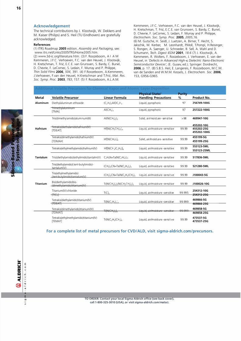
Additional Volatile Precursors for Chemical Vapor and Atomic Layer Deposition
Metal Volatile Precursor Linear FormulaPhysical State/Handling Precautions
Purity% Product No.
Aluminum Diethylaluminum ethoxide (C2H5)2AlOC2H5 Liquid, pyrophoric 97 5679-100G
Trimethylaluminum[TMA]
Al(CH3)3 Liquid, pyrophoric 97 57-100G
Tris(dimethylamido)aluminum(III) Al(N(CH3)2)3 Sol id, air/moisture -sensitive >98 6997-10G
HafniumTetrakis(diethylamidohanium(IV)[TDEAT]
H[N(CH2CH3)2]4 Liquid, air/moisture -sensitive 99.99550-10G550-5G550-100G
Tetrakis(dimethylamido)hanium(IV)
[TDMAH]H[N(CH3)2]4 Solid, air/moisture -sensitive 99.99
55199-5G
55199-5G
Tetrakis(ethylmethylamido)hanium(IV) H[N(CH3)C2H5)]4 Liquid, air/moisture -sensitive 99.9955313-5ML
55313-5ML
Tantalum Tris(diethylamido)(ethylimido)tantalm(V) C2H5N=Ta(N(C2H5)2)3 Liquid, air/moisture -sensitive 99.99 517836-5ML
Tris(diethylamido)( tert -butylimido)-tantalum(V)
(CH3)3CN=Ta(N(C2H5)2)3 Liquid, air/moisture -sensitive 99.99 5180-5ML
Tris(ethylmethylamido)(tert -butylimido)tantalum(V)
(CH3)3CN=Ta(N(C2H5)CH3)3 Liquid, air/moisture -sensitive 99.99 J10003-5G
TitaniumBis(diethylamido)bis-(dimethylamido)titanium(IV)
Ti(N(CH3)2)2(N(CH2CH3)2)2 Liquid, air/moisture -sensitive 99.99 J10006-10G
Titanium(IV) chloride
[TICL]TiCl4 Liquid, air/moisture -sensitive 99.995
531-10G
531-5G
Tetrakis(diethylamido)titanium(IV)[TDEAT]
Ti[N(C2H5)2]4 Liquid, air/moisture -sensitive 99.99969866-5G
69866-5G
Tetrakis(dimethylamido)titanium(IV)[TDMAT]
Ti[N(CH3)2]4 Liquid, air/moisture -sensitive 99.99969858-5G
69858-5G
Tetrakis(ethylmethylamido)titanium(IV)[TEMAT]
Ti(N(C2H5)CH3)4 Liquid, air/moisture -sensitive 99.9973537-5G73537-5G
For a complete list of metal precursors for CVD/ALD, visit sigma-aldrich.com/precursors.
S i l i c o n - B a s e d P a s s i v e a n d
S y s t e m - i n - P a c k a g e
8/14/2019 Deposition of Ceramic and Hybrid Materials - Material Matters v1n3
http://slidepdf.com/reader/full/deposition-of-ceramic-and-hybrid-materials-material-matters-v1n3 17/20
For questions, product data, or new product suggestions,please contact the Materials Science team at [email protected].
O
r d
er :
1
. 8
0
0
. 3
2
5
. 3
0
1
0
T e
c h
n
i c a
l
S e
r vi c e
:
1
. 8
0
0
.2
3
1
. 8
3 2
7
17
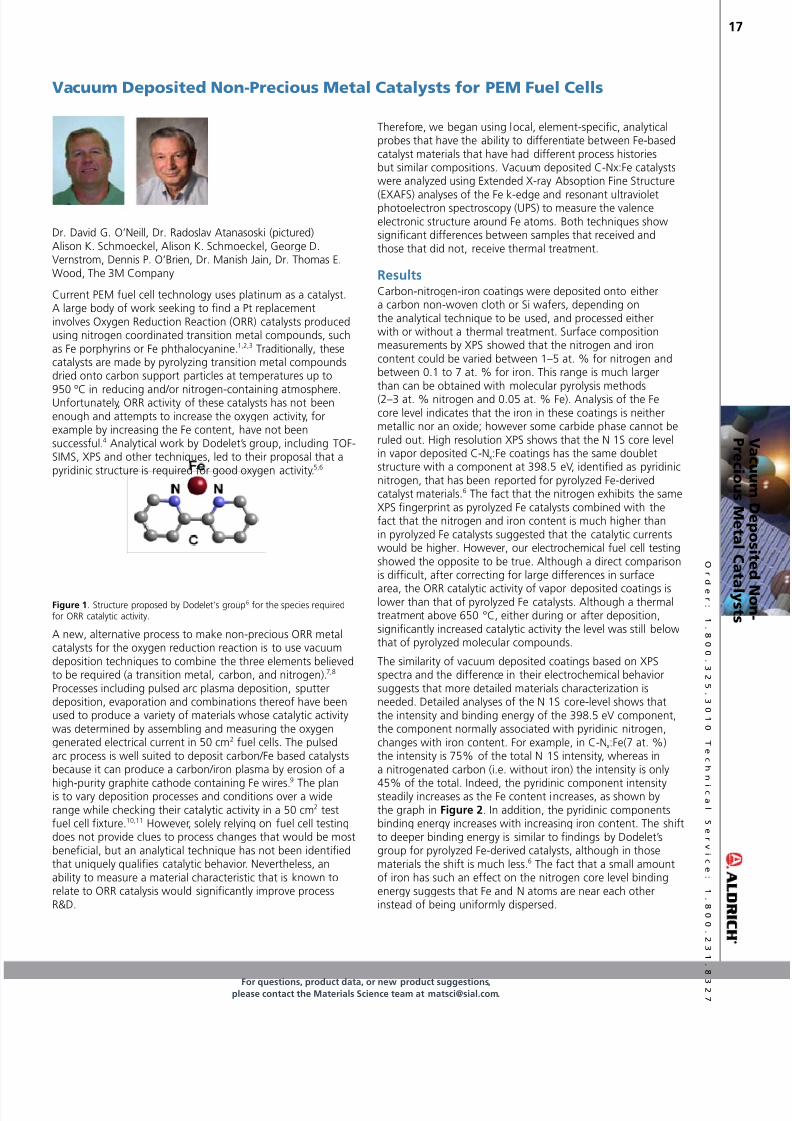
Dr. David G. O’Neill, Dr. Radoslav Atanasoski (pictured)Alison K. Schmoeckel, Alison K. Schmoeckel, George D.Vernstrom, Dennis P. O’Brien, Dr. Manish Jain, Dr. Thomas E.Wood, The 3M Company
Current PEM uel cell technology uses platinum as a catalyst.A large body o work seeking to ind a Pt replacementinvolves Oxygen Reduction Reaction (ORR) catalysts producedusing nitrogen coordinated transition metal compounds, suchas Fe porphyrins or Fe phthalocyanine.1,2,3 Traditionally, thesecatalysts are made by pyrolyzing transition metal compoundsdried onto carbon support particles at temperatures up to
950 ºC in reducing and/or nitrogen-containing atmosphere.Unortunately, ORR activity o these catalysts has not beenenough and attempts to increase the oxygen activity, orexample by increasing the Fe content, have not beensuccessul.4 Analytical work by Dodelet’s group, including TOF-SIMS, XPS and other techniques, led to their proposal that apyridinic structure is required or good oxygen activity.5,6
Figure 1. Structure proposed by Dodelet’s group6 or the species requiredor ORR catalytic activity.
A new, alternative process to make non-precious ORR metalcatalysts or the oxygen reduction reaction is to use vacuumdeposition techniques to combine the three elements believedto be required (a transition metal, carbon, and nitrogen).7,8 Processes including pulsed arc plasma deposition, sputterdeposition, evaporation and combinations thereo have beenused to produce a variety o materials whose catalytic activitywas determined by assembling and measuring the oxygengenerated electrical current in 50 cm2 uel cells. The pulsedarc process is well suited to deposit carbon/Fe based catalystsbecause it can produce a carbon/iron plasma by erosion o a
high-purity graphite cathode containing Fe wires.9
The planis to vary deposition processes and conditions over a widerange while checking their catalytic activity in a 50 cm2 testuel cell ixture.10,11 However, solely relying on uel cell testingdoes not provide clues to process changes that would be mostbeneicial, but an analytical technique has not been identiiedthat uniquely qualiies catalytic behavior. Nevertheless, anability to measure a material characteristic that is known torelate to ORR catalysis would signiicantly improve processR&D.
Thereore, we began using local, element-speciic, analyticalprobes that have the ability to dierentiate between Fe-basedcatalyst materials that have had dierent process historiesbut similar compositions. Vacuum deposited C-Nx:Fe catalystswere analyzed using Extended X-ray Absoption Fine Structure
(EXAFS) analyses o the Fe k-edge and resonant ultravioletphotoelectron spectroscopy (UPS) to measure the valenceelectronic structure around Fe atoms. Both techniques showsigniicant dierences between samples that received andthose that did not, receive thermal treatment.
ResultsCarbon-nitrogen-iron coatings were deposited onto eithera carbon non-woven cloth or Si waers, depending onthe analytical technique to be used, and processed eitherwith or without a thermal treatment. Surace compositionmeasurements by XPS showed that the nitrogen and ironcontent could be varied between 1–5 at. % or nitrogen andbetween 0.1 to 7 at. % or iron. This range is much largerthan can be obtained with molecular pyrolysis methods(2–3 at. % nitrogen and 0.05 at. % Fe). Analysis o the Fecore level indicates that the iron in these coatings is neithermetallic nor an oxide; however some carbide phase cannot beruled out. High resolution XPS shows that the N 1S core levelin vapor deposited C-Nx:Fe coatings has the same doubletstructure with a component at 398.5 eV, identiied as pyridinicnitrogen, that has been reported or pyrolyzed Fe-derivedcatalyst materials.6 The act that the nitrogen exhibits the sameXPS ingerprint as pyrolyzed Fe catalysts combined with theact that the nitrogen and iron content is much higher thanin pyrolyzed Fe catalysts suggested that the catalytic currentswould be higher. However, our electrochemical uel cell testingshowed the opposite to be true. Although a direct comparisonis diicult, ater correcting or large dierences in surace
area, the ORR catalytic activity o vapor deposited coatings islower than that o pyrolyzed Fe catalysts. Although a thermaltreatment above 650 °C, either during or ater deposition,signiicantly increased catalytic activity the level was still belowthat o pyrolyzed molecular compounds.
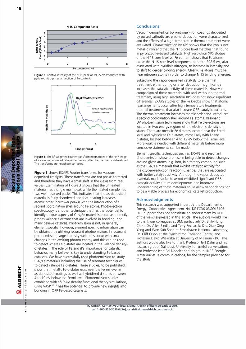
The similarity o vacuum deposited coatings based on XPSspectra and the dierence in their electrochemical behaviorsuggests that more detailed materials characterization isneeded. Detailed analyses o the N 1S core-level shows thatthe intensity and binding energy o the 398.5 eV component,the component normally associated with pyridinic nitrogen,changes with iron content. For example, in C-Nx:Fe(7 at. %)the intensity is 75% o the total N 1S intensity, whereas ina nitrogenated carbon (i.e. without iron) the intensity is only
45% o the total. Indeed, the pyridinic component intensitysteadily increases as the Fe content increases, as shown bythe graph in Figure . In addition, the pyridinic componentsbinding energy increases with increasing iron content. The shitto deeper binding energy is similar to indings by Dodelet’sgroup or pyrolyzed Fe-derived catalysts, although in thosematerials the shit is much less.6 The act that a small amounto iron has such an eect on the nitrogen core level bindingenergy suggests that Fe and N atoms are near each otherinstead o being uniormly dispersed.
Vacuum Deposited Non-Precious Metal Catalysts for PEM Fuel Cells
V a c u um D e p o si t e d
N on-
P r e c i o u s M e t al C a t al y s t s
8/14/2019 Deposition of Ceramic and Hybrid Materials - Material Matters v1n3
http://slidepdf.com/reader/full/deposition-of-ceramic-and-hybrid-materials-material-matters-v1n3 18/20
TO ORDER: Contact your local Sigma-Aldrich office (see back cover),call 1-800-35-3010 (USA), or visit sigma-aldrich.com/matsci.
s i g
m
a - a l d r i c h
. c o m
18
V a c u
u m D e p o s i t e d N o n -
P r e c i o u s M e t a l C a t a l y s t s
N 1S Component Ratio
0
1
2
3
4
5
6
0 2 4 6 8
Fe content (at %)
R a t i o
( 3 9 8 e V
P e a k ) / ( 4 0 0 e V P
e a k )
Figure . Relative intensity o the N 1S peak at 398.5 eV associated withpyridinic nitrogen as a unction o Fe content.
Heat treatment effect
T r a n s f o r m m
a g n i t u d e
R (Angstroms)
2 4
Without heat treatment
After heat treatment
Figure 3. The k3-weighted Fourier transorm magnitudes o the Fe K-edgeo a vacuum deposited catalyst beore and ater the thermal post-treatment.The transorms are not phase-corrected.
Figure 3 shows EXAFS Fourier transorms or vacuumdeposited catalysts. These transorms are not phase-correctedand thereore they have a small shit in the x-axis rom realvalues. Examination o Figure 3 shows that the unheatedmaterial has a single main peak while the heated sample hastwo well-resolved peaks. This indicates that the as-depositedmaterial is airly disordered and that heating increasesatomic order (narrower peaks) with the introduction o asecond coordination shell around Fe atoms. Photoelectronspectroscopy is another technique that has the potential toidentiy unique aspects o C-Nx:Fe materials because it directlyprobes valence electrons that are involved in bonding, andmany believe catalysis. Photoemission is not, in general,element speciic, however, element speciic inormation canbe obtained by utilizing resonant photoemission. In resonantphotoemission, large intensity variations occur with smallchanges in the exciting photon energy and this can be used
to detect where Fe d-states are located in the valence density-o-states.12 The role o Fe and it’s importance or catalyticbehavior, many believe, is key to understanding Fe-basedcatalysts. We have successully used photoemission to studyC-Nx:Fe materials including the use o resonant techniquesto detect valence Fe d-states. These studies, to be published,show that metallic Fe d-states exist near the Fermi level inas-deposited coatings as well as hybridized d-states between4 to 10 eV below the Fermi level. Photoemission studiescombined with ab initio density unctional theory simulations,using VASP,12,13 has the potential to provide new insights intobonding in ORR Fe-based catalysts.
Conclusions
Vacuum deposited carbon-nitrogen-iron coatings depositedby pulsed cathodic arc plasma deposition were characterizedand the eects o a high temperature thermal treatment wereevaluated. Characterization by XPS shows that the iron is notmetallic iron and that the N 1S core level matches that oundin pyrolyzed Fe-based catalysts. High resolution XPS studieso the N 1S core level vs. Fe content shows that Fe atoms
cause the N 1S core level component at about 398.5 eV, alsoassociated with pyridinic nitrogen, to increase in intensity andto shit to deeper binding energy. Clearly, Fe atoms must benear nitrogen atoms in order to change N 1S binding energies.
Subjecting the vapor deposited catalysts to a thermaltreatment, either during or ater deposition, signiicantlyincreases the catalytic activity o these materials. However,comparison o these materials, with and without a thermaltreatment, using high resolution XPS does not show signiicantdierences. EXAFS studies o the Fe k-edge show that atomicrearrangements occur ater high temperature treatments,thermal treatments that also increase ORR catalytic currents.The thermal treatment increases atomic order and introducesa second coordination shell around Fe atoms. Resonant
UV photoemission techniques show that Fe d-electrons arelocated in two energy regions o the electronic density ostates. There are metallic Fe d-states located near the Fermilevel and hybridized Fe d-states, most likely with ligandp-states, located between 4 to 12 eV below the Fermi level.More work is needed with dierent materials beore moreconclusive statements can be made.
Element speciic techniques such as EXAFS and resonantphotoemission show promise in being able to detect changesaround given atoms, e.g. iron, in a ternary compound suchas the C-Nx:Fe materials that exhibit catalytic activity orthe oxygen-reduction reaction. Changes that are associatedwith better catalytic activity. Although the vapor depositedmaterials made so ar have not exhibited signiicant ORR
catalytic activity, uture developments and improvedunderstanding o these materials could allow vapor depositionto be a viable process or economical catalyst production.
AcknowledgmentsThis research was supported in part by the Department oEnergy, Cooperative Agreement No. DE-FC36-03GO13106.DOE support does not constitute an endorsement by DOEo the views expressed in this article. The authors would liketo thank our colleagues at 3M, particularly Dr. Shih-HungChou, Dr. Allen Siedle, and Terry Pechacek; Drs. Xiao-QingYang and Won-Sub Soon at Brookhaven National Laboratory;Dr. Cli Olson at the Synchrotron Radiation Center; andProessor David Wieliczka at University o Missouri - KC. Theauthors would also like to thank Proessor Je Dahn and hisresearch group, Dalhousie University, or useul conversations,and Proessor Jean-Pol Dodelet and his group, INRS-Energie,Materiaux et Telcommunications, or the samples provided orthis study.
8/14/2019 Deposition of Ceramic and Hybrid Materials - Material Matters v1n3
http://slidepdf.com/reader/full/deposition-of-ceramic-and-hybrid-materials-material-matters-v1n3 19/20
For questions, product data, or new product suggestions,please contact the Materials Science team at [email protected].
O
r d
er :
1
. 8
0
0
. 3
2
5
. 3
0
1
0
T e
c h
n
i c a
l
S e
r vi c e
:
1
. 8
0
0
.2
3
1
. 8
3 2
7
19
References and Note(1) Terminology Convention: “pyrolyzed, Fe-derived” willreer to the catalyst syntheses using Fe containing molecules,such as Fe porphoryns, Fe phthalocyanines, Fe-acetate,etc. (2) N4-Macrocyclic Metal Complexes: Electrocatalysis,Electrophotochemistry & Biomimetic Electroanalysis. Edited byJ. Zagal, F. Bedioui, and J. P. Dodelet, Springer 006. (3) H. A.Gasteiger, S. S. Kocha, B. Sompalli, F. T. Wagner, Applied Cat. B:Environ., 005, 9, 56. (4) J.-P. Dodelet in N4-Macrocyclic Metal
Complexes: Electrocatalysis, Electrophotochemistry & BiomimeticElectroanalysis. Edited by J. Zagal, F. Bedioui, and J. P. Dodelet,Springer 006. (5) F. Jaouen, M. Leevre, J.-P. Dodelet, and M. Cai,
J. Phys. Chem. B, 006, 5553, 110. (6) F. Jaouen, S. Marcott, J.-P.Dodelet and G. Lindbergh, J. Phys. Chem. B, 003, 1376, 107. (7)R.T. Atanasoski, Novel Approach to Non-Precious Metal Catalysts,DOE Hydrogen Program FY 00 Progress Report (V.C.5).
(8) G. Lalande, D. Guay, J. P. Dodelet, S. A. Majetich,M.E.McHenry, Chem. Mater., 1997, 784, 9. E. Bradley Easton,Arman Bonakdarpour, and J.R. Dahn, Electrochem. and Solid-State Lett ., 006, A463, 9. (9) E.I. Tochitsky, O.V. Selianov,V.V. Akulich, I.A. Kapustin and A.V. Stanishevskii,Surface and Coatings Technology , 1991 522, 47.(10) R.T. Atanasoski, Novel Approach to Non-Precious Metal Catalysts, DOE Hydrogen Program FY 005 Progress Report (V.C.5).(11) R.T. Atanasoski, Novel Approach to Non-Precious Metal
Catalysts, DOE Hydrogen Program FY 006 Progress Report. (12)G. Kresse and J. Haner, Phys. Rev. B, 7, 558 (1993); G. Kresseand J. Furthmüller, Phys. Rev. B, 1996, 11169, 54. G. Kresse andJ. Furthmüller, Comput. Mater. Sci., 1996, 15, 6. G. Kresse and D.Joubert, Phys. Rev. B, 1999, 1758, 59. (13) M. Jain, S.-H. Chou, A.Siedle, J. Phys. Chem. B, 006, 4179, 110.
High-Purity Graphite and Iron
Materials Physical Form Size/density Purity (%) Product No.
Iron Wire diam. 0.5 mm 99.99 668-7.5G
diam. 1.0 mm 99.996656-3.1G6656-15.5G
diam. 0.5 mm 99.935683-1.5G
35683-7.5G
diam. 1.0 mm 99.93568-6.G3568-31G
Foil thickness 0.25 mm 99.9933811-1.G33811-5G
thickness 0.1 mm 99.9356808-G356808-8G
Granule 10–40 mesh 99.9991305-5G1305-5G
Rod diam. 6.3 mm 99.986613-30G6613-150G
Graphite Rod length 150 mm, diam. 3 mm, low density 99.999 96537-3.5G
length 150 mm, diam. 3 mm, high density 99.995 9655-60G
length 150 mm, diam. 6 mm, low density 99.999 96553-180.7G
length 150 mm, diam. 6 mm, high density 99.995 96561-0.5G
Safe and Simple• Gas dispensing and storage in one compact, portable system
• Keeps lecture-bottles upright and stable, eliminates tip-over
• Reduces equipment damage and chance o personal injury
• Choice o our models matched to the application
• Wall-mountable
• Express Service™ Program or ast cleaning, repair, or component
replacement
Order Information
Description Prod. No.Non-Corrosive Lecture-Bottle Station Z56599-1EA 825.00
High-Purity Lecture-Bottle Station Z5660-1EA 995.00
Lecture-Bottle Station with T-Purge Valve Z56610-1EA 1,350.00
Corrosive Lecture-Bottle Station with Cross-Purge Valve Z5669-1EA 2,625.00
Lecture-Bottle Service Station Z56637-1EA 460.00
Visit our Web site or a brochure with complete inormation about these new Lecture-Bottle dispensing stations,including a Station Selection Guide that matches the correct station to the gas you are using.
sigma-aldrich.com/gases
SIGMA-ALDRICH LECTURE-BOTTLE STATIONS Safe and Simple Systems for Dispensing Lecture-Bottle Gases
Dispensing lecture-bottle gases has never been saer or simpler using these
portable lecture-bottle stations. The premium quality components housedwithin a station are matched to the application, ully assembled, leak-tested, and ready or use. Just connect the station to the lecture-bottle,
process, and a source o inert gas i using a station with a purge valve, andyou are ready to go.
V a c u um D e p o si t e d
N on-
P r e c i o u s M e t al C a t al y s t s
8/14/2019 Deposition of Ceramic and Hybrid Materials - Material Matters v1n3
http://slidepdf.com/reader/full/deposition-of-ceramic-and-hybrid-materials-material-matters-v1n3 20/20
Acceleatn Customes’ Success
tou Leaesp n Lie Science ,
High Technology an Service
ArgentinaSIGMA-ALDRICHDEARGENTINA,S.A.Tel:541145561472Fax:541145521698
AustraliaSIGMA-ALDRICHPTy.,LIMITEDFreeTel:1800800097FreeFax:1800800096Tel:61298410555Fax:61298410500
Austria
SIGMA-ALDRICHHANDELSGmbHTel:4316058110Fax:4316058120
BelgiumSIGMA-ALDRICHNV/SA.FreeTel:0800-14747FreeFax:0800-14745Tel:038991301Fax:038991311
BrazilSIGMA-ALDRICHBRASILLTDA.Tel:55113732-3100Fax:55113733-5151
Canada
SIGMA-ALDRICHCANADALTD.FreeTel:800-565-1400FreeFax:800-265-3858Tel:905-829-9500Fax:905-829-9292
ChinaSIGMA-ALDRICH(SHANGHAI)TRADINGCo.LTD.Tel:+86-21-61415566Fax:+86-21-61415567
Czech RepublicSIGMA-ALDRICHS.R.o.Tel:+420246003200Fax:+420246003291
Denmark
SIGMA-ALDRICHDENMARkA/STel:43565910Fax:43565905
Finland
SIGMA-ALDRICHFINLANDTel:(09)3509250Fax:(09)35092555
FranceSIGMA-ALDRICHCHIMIES.à.r.l.Telappelgratuit:0800211408
Faxappelgratuit:0800031052
GermanySIGMA-ALDRICHCHEMIEGmbHFreeTel:0800-5155000FreeFax:0800-6490000
Greece
SIGMA-ALDRICH(o.M.)LTDTel:302109948010Fax:302109943831
Hungary
SIGMA-ALDRICHktTel:06-1-235-9054Fax:06-1-269-6470Ingeneszöldtelen:06-80-355-355
Ingeneszöldax:06-80-344-344
India
SIGMA-ALDRICHCHEMICALSPRIVATELIMITEDTelephneBangalre:91-80-6621-9600NewDelhi:91-11-4165-4255Mumbai:91-22-2570-2364Hderabad:91-40-6684-5488FaxBangalre:91-80-6621-9650NewDelhi:91-11-4165-4266Mumbai:91-22-2579-7589Hderabad:91-40-6684-5466
Ireland
SIGMA-ALDRICHIRELANDLTD.FreeTel:1800200888FreeFax:1800600222Tel:35314041900Fax:35314041910
Israel
SIGMA-ALDRICHISRAELLTD.FreeTel:1-800-70-2222Tel:08-948-4100Fax:08-948-4200
ItalySIGMA-ALDRICHS.r.l.Telen:0233417310Fax:0238010737NumerVerde:800-827018
Japan
SIGMA-ALDRICHJAPANk.k.TTel:0357967300TFax:0357967315
Korea
SIGMA-ALDRICHkoREATel:031-329-9000Fax:031-329-9090
Malaysia
SIGMA-ALDRICH(M)SDN.BHDTel:603-56353321Fax:603-56354116
Mexico
SIGMA-ALDRICHQUÍMICA,S.A.deC.V. FreeTel:01-800-007-5300FreeFax:01-800-712-9920
The Netherlands
SIGMA-ALDRICHCHEMIEBVTelGratis:0800-0229088FaxGratis:0800-0229089Tel:078-6205411Fax:078-6205421
New Zealand
SIGMA-ALDRICHPTy.,LIMITED
FreeTel:0800936666
FreeFax:0800937777
Tel:61298410500
Fax:61298410500
Norway
SIGMA-ALDRICHNoRWAyAS
Tel:23176060
Fax:23176050
Poland
SIGMA-ALDRICHSp.z..
Tel:0618290100
Fax:0618290120
Portugal
SIGMA-ALDRICHQUÍMICA,S.A.
FreeTel:800202180
FreeFax:800202178
Tel:219242555
Fax:219242610
Russia
SIGMA-ALDRICHRUS,LLC
Tel:+7(495)621-5828/5923/6037
Fax:+7(495)621-5828/5923/6037
Singapore
SIGMA-ALDRICHPTE.LTD.
Tel:65-67791200
Fax:65-67791822
South Africa
SIGMA-ALDRICH
SoUTHAFRICA(PTy)LTD.
FreeTel:0800110075
FreeFax:0800110079
Tel:27119791188
Fax:27119791119
Spain
SIGMA-ALDRICHQUÍMICA,S.A.
FreeTel:900101376
FreeFax:900102028
Tel:916619977
Fax:916619642
Sweden
SIGMA-ALDRICHSWEDENAB
Tel:020-350510
Fax:020-352522
outsideSwedenTel:+4687424200
outsideSwedenFax:+4687424243
Switzerland
SIGMA-ALDRICHCHEMIEGmbH
SwissFreeCall:0800800080
Tel:+41817552828
Fax:+41817552815
United Kingdom
SIGMA-ALDRICHCoMPANyLTD.
FreeTel:0800717181
FreeFax:0800378785
Tel:01747833000
Fax:01747833313
SAFC(Uk):01202712305
United States
SIGMA-ALDRICH
P.o.Bx14508
St.Luis,Missuri63178
Tll-Free:(800)325-3010
CallCllect:(314)771-5750
Tll-FreeFax:(800)325-5052
Tel:(314)771-5765
Fax:(314)771-5757
Internet
sigma-aldrich.cm
JCU01671-503403
0116
Te SigMA-ALdriCh goup
World Headquarters3050 Spruce St., St. Louis, MO 63103
(314) 771-5765
sigma-aldrich.com
Order/Customer Service (800) 325-3010 • Fax (800) 325-5052
Technical Service (800) 325-5832 • sigma-aldrich.com/techservice
Development/Bulk Manufacturing Inquiries (800) 244-1173
©2006 Sigma-Aldrich Co. All rights reserved.SIGMA,-, SAFC, , SIGMA-ALDRI CH, ), ISOTEC, ALDRICH, ^, FLUKA, T, and SUPELCO are trademarks belonging to Sigma-Aldrich Co. and its ailiateSigma-Aldrich Biotechnology, L.P. Riedel-de Haën® trademark under license rom Riedel-de Haën GmbH. Sigma brand products are sold through Sigma-Aldrich, Inc.Sigma-Aldrich, Inc. warrants that its products conorm to the inormation contained in this and other Sigma-Aldrich publications. Purchaser must determine the suitability othe product(s) or their particular use. Additional terms and conditions may apply. Please see reverse side o the invoice or packing slip.
3050 Spruce Street • St. Louis, MO 63103 USA
Return Service Requested
PRESORTEDSTANDARD
U.S. POSTAGE
PAIDSIGMA-ALDRICHCORPORATION