deposition and characterization of ceramic thin films and
TRANSCRIPT

Louisiana State UniversityLSU Digital Commons
LSU Doctoral Dissertations Graduate School
2015
Deposition and Characterization of Ceramic ThinFilms and a New Experimental Approach toEvaluate the Mechanical Integrity of Film/Substrate Interfacial LayersYang MuLouisiana State University and Agricultural and Mechanical College
Follow this and additional works at: https://digitalcommons.lsu.edu/gradschool_dissertations
Part of the Mechanical Engineering Commons
This Dissertation is brought to you for free and open access by the Graduate School at LSU Digital Commons. It has been accepted for inclusion inLSU Doctoral Dissertations by an authorized graduate school editor of LSU Digital Commons. For more information, please [email protected].
Recommended CitationMu, Yang, "Deposition and Characterization of Ceramic Thin Films and a New Experimental Approach to Evaluate the MechanicalIntegrity of Film/Substrate Interfacial Layers" (2015). LSU Doctoral Dissertations. 1427.https://digitalcommons.lsu.edu/gradschool_dissertations/1427

i
DEPOSITION AND CHARACTERIZATION OF CERAMIC THIN
FILMS AND A NEW EXPERIMENTAL APPROACH TO EVALUATE
THE MECHANICAL INTEGRITY OF FILM/SUBSTRATE
INTERFACIAL LAYERS
A Dissertation
Submitted to the Graduate Faculty of the
Louisiana State University and
Agricultural and Mechanical College
in partial fulfillment of the
requirements for the degree of
Doctor of Philosophy
in
The Department of Mechanical Engineering
by
Yang Mu
B.S., Beijing Institute of Technology, 2006
August 2015

ii
This thesis is dedicated to my beloved grandmother
iii
ACKNOWLEDGEMENTS
I would like to express my deepest and grateful thanks to my committee chair,
also my advisor, Dr Wen Jin Meng. You not only taught me the knowledge printed in the
textbook, but also how to be a qualified researcher in science and engineering. I can’t
remember how many times you have spent with me in the lab to teach me from simply
how to use a wrench to operate a sophisticated high-value instrument with patience and
energy. Your experise, guidance, and caring encouraged me to overcome every difficulty
I have encountered and to finally reach this success of my life.
I would like to give my appreciation to Dr Sunggook Park, Dr Dorel Moldovan,
and Dr George Z. Voyiadjis, my committee members for their guidance and disscussion.
I would also like to thank all my lab mates I have worked with: Dr. Ke Chen, Dr.
Bin Lu, Dr. Fanghua Mei, Dr. Jin Jiang, Paul Hymel, and Bin Zhang. I wish to thank all
ME staff members and Drs. Dongmei Cao and Clayton Loehn of the LSU Institute of
Advanced Materials (IAM) Shared Instrumentation Facility (SIF). I wish to thank Yi Du,
Cheng Zhang and many more friends. I could never have accomplished this dissertation
all by myself without your kind advice and support.
Professor John W. Hutchinson of Harvard University has kindly supplied a strain
gradient plasticity analysis of the experimental data described in Chapter 6, for which I
am most grateful.
Finally, my thank goes out to my parents, I would be nothing without your caring,
support, and endless love.
This research would have not been possible without the financial assistance from
Louisana State University, the Louisiana Board of Regents, and the U.S. National

iv
Science Foundation, under contracts LEQSF(2011-13)-RD-B-03, LEQSF(2011-13)-RD-
B-04, LEQSF(2013-16)-RD-B-01 and grant CMMI-0900167.
v
TABLE OF CONTENTS
ACKNOWLEDGEMENTS ...............................................................................................iii
ABSTRACT .....................................................................................................................vii
CHAPTER 1 INTRODUCTION..................................... .................................1
1.1 Applications of Thin Films in Macro-Scale Devices…………………………1
1.2 Applications of Thin Films in Micro-Scale Devices and Microfabrication…1
1.3 Thin Film Deposition Technologies………………………………………….2
1.3.1 DC Sputtering…...…………………………..………………….…4
1.3.2 DC Magnetron Sputtering…………………………………………5
1.3.3 Plasma Assisted Sputtering………………………………...………..6
1.3.4 Reactive Sputtering…………………………..……………………6
1.4 Thin Film Adhesion Tests………………………………….…………………7
1.5 Size Effect in Thin Film Interlayer………..…………………………………..9
1.6 Outline of the Dissertation…………………………………...…...………….11
1.7 References……………………………………….…………………………12
CHAPTER 2 DESIGN AND CONSTRUCTION OF A HIGH-DENSITY PLASMA
ASSISTED ULTRA HIGH VACUUM (UHV) PHYSICAL VAPOR
DEPOSITION (PVD)SYSTEM……………………...………….………16
2.1 Vacuum System……………………………………………………………16
2.2 Sample Transfer Mechanism……………………………………………...…19
2.3 Heating Stage……………….………………………………………………..21
2.4 Thin Film Deposition……………...…………………………………………21
2.5 References……………………………………………………………………22
CHAPTER 3 LOW TEMPERATURE DEPOSITION TITANIUM BORIDE THIN
FILMS AND THEIR APPLICATION TO SURFACE ENGINEERING
OF MICROSCALE MOLD INSERT……..………………..……………23
3.1 Introduction…………………..………………………………………………23
3.2 Experimental Procedures…………………………………………….………24
3.3 Results and Discussion………………………………………………………29
3.4 References……………………………………………………………………40
CHAPTER 4 TWO METHODS OF MEASURING INTERFACIAL SHEAR
STRESS……………………………………………..………………...…43
4.1 Introduction…………………………………………………………………43
4.2 Experimental Procedures……………………………………………………44
4.3 Results and Discussion………………………………………………………46
4.4 References……………………………………………………………………56
CHAPTER 5 THICKNESS DEPENDENCE OF FLOW STRESS OF CU THIN
FILMS IN CONSTRAINED SHEAR PLASIC FLOW….……………...57
5.1 Introduction…………………………………………………………………57
vi
5.2 Experimental Procedures……………………………………………………58
5.3 Results and Discussion………………………………………………………60
5.4 References……………………………………………………………………68
CHAPTER 6 MICRO-PILLAR MEASUREMENT OF PLASTICITY IN
CONFINED CU THIN FILMS………….………………………………70
6.1 Introduction…………………………………………………………..………70
6.2 Deposition and Structural Characterization of Polycrystalline CrN and Cu
Thin Films……………………………………..…………………………………71
6.3 Instrumented Indentation of Polycrystalline Cu and CrN Films……...……81
6.4 Micro-Pillar Preparation and Compression Test………………………..……85
6.5 The Material Length Parameter and Trends Predicted by Strain Gradient
Plasticity………………..………….………………………………………..……93
6.6 Concluding Remarks………..………..………………………………………96
6.7 References……..…………………………………………………..…………98
CHAPTER 7. SUMMARY……………………………………………………………102
APPENDIX. LETTERS OF COPYRIGHT PERMISSION…………………………103
VITA…………………………………………………………………………………....105

vii
ABSTRACT
Due to their corrosion resistance, high temperature stability, high strength, and
high hardness, refractory ceramic thin films and coatings have been utilized for surface
engineering of mechanical components and mechanical fabrication tools. Adhesion
between ceramic thin films and coatings and the substrate is of critical concern for
performance and life time of coated systems. In this dissertation, a custom designed and
constructed ultra-high-vacuum (UHV) vapor phase deposition system was used for the
preparation of ceramic thin films through low-pressure high-density plasma assisted
physical vapor deposition (PVD) methods. Deposited thin films were characterized by
X-ray photoelectron spectroscopy (XPS), X-ray diffraction (XRD), instrumented
nanoindentation, focus ion beam (FIB) scanning electron microscope (FIB SEM), and
transmission electron microscope (TEM). The effective interfacial shear strength
between TiN and CrN thin films and their substrates was evaluated through a substrate-
tension method and a newly introduced experimental testing method involving FIB
script-milling of film/substrate specimens into micro-pillars and instrumented
compression testing performed on such micro-pillars. This micro-pillar testing protocol
was further used to experimentally demonstrate, for the first time to our knowledge, a
size effect in the shear strength in the configuration of confined shear plastic flow of
ductile thin layers. This latter experiment furnishes new and fundamental data for micron
scale plasticity theories.

1
CHAPTER 1
INTRODUCTION
1.1 Applications of Thin Films in Macro-Scale Devices
Thin films are widely used in surface engineering to improve the performance of the
near-surface region by modifying the surface chemical and mechanical properties. For example,
diamond-like carbon (DLC) coatings are an excellent candidate for application to automotive
engines due to their low boundary friction, good wear resistance, and suitability to serve as a
solid lubricant [1]. DLC also improves the tribological performance of die/metal-piece systems
[2]. Highly hydrogenated DLC deposited by PACVD is a potential coating material for the ball
bearings for aerospace craft because of its low friction and long wear time in both vacuum and
in-air environments [3]. Thermal barrier coatings (TBCs) are considered as the candidate layer
for aerospace sandwich panels [4]. A critical requirement for all these applications is high
quality bonding between the coating and the substrate. Quantitative evaluation of the mechanical
integrity of the interface region between coatings and substrates is therefore important.
1.2 Applications of Thin Films in Micro-Scale Devices and Microfabrication
The global microelectromechanical systems (MEMS) market has grown from its infancy
in early 1980s [5] to be worth about ten billion U.S. dollars in 2011 [6]. So far, major categories
of commercialized MEMS devices, including pressure sensors, accelerometers, gyroscopes,
deflectable optical mirrors, have been fabricated from Si-based materials following protocols
developed for integrated circuit processing industries [ 7 ]. Although metal-/alloy- based
microsystems products are much rarer at present, their unique collection of physical properties
enables construction of certain microdevices with either performance advantages over Si-based
counterparts or no Si-based analogs at all. Piezoelectric Pb(Zr, Ti)O3 (PZT) thin films have been
vapor deposited directly onto 50μm thick Ti substrates [ 8 ]. Using the PZT/Ti materials

2
combination, MEMS scanner mirrors have been built with increased fracture resistance as
compared to Si-based counterparts [ 9 ]. Free-standing microscale structures made of
electrodeposited Co-Ni alloys have been demonstrated, with soft magnetic properties suitable for
magnetic field actuation [10]. Micro grippers and other microscale actuators are enabled by the
use of shape memory alloys in microsystems [ 11]. Wings for micro aerial vehicles were
fabricated out of the Ti-6Al-4V alloy because of its mechanical properties [ 12 ]. The
incorporation of metals/alloys into microsystems enables different device configurations/designs,
and metal-based microsystem products hold promise technologically for improved performance
or expanded functionality and commercially for additional applications and associated revenue
streams.
In addition to microscale actuators and sensors, the continued trend towards
miniaturization of electronic and medical devices demands efficient manufacturing of small
metal-based parts, including miniaturized connector pins, sockets, screws, springs, etc [13]. To
satisfy such demands, there are ongoing efforts focused on extending macroscale metal forming
technologies down to the microscale [13,14]. Studies of micro bending [15], micro extrusion
[16], and micro die upsetting [17] have all been conducted.
1.3 Thin Film Deposition Technologies
Over the last century, a variety of thin film deposition techniques have been developed
with the development of vacuum technologies and plasma technologies. The general
classification of deposition process was divided into four different groups: gaseous state
processes, solution state processes, molten or semi-molten state processes, and solid state
processes [18].
3
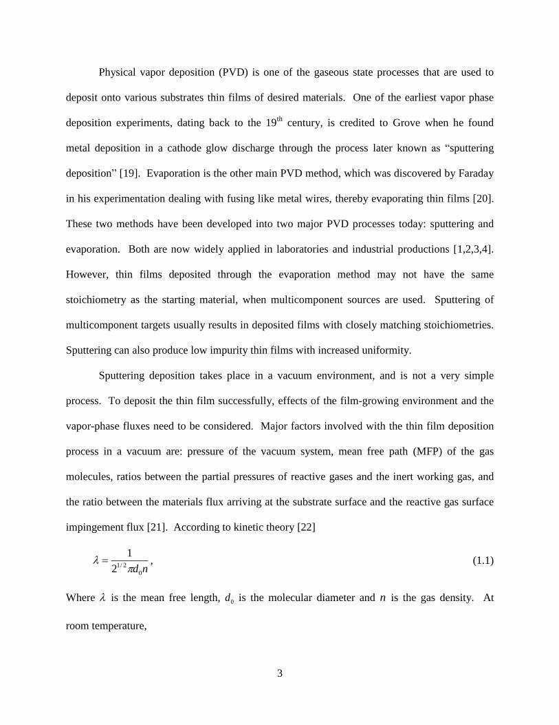
Physical vapor deposition (PVD) is one of the gaseous state processes that are used to
deposit onto various substrates thin films of desired materials. One of the earliest vapor phase
deposition experiments, dating back to the 19th
century, is credited to Grove when he found
metal deposition in a cathode glow discharge through the process later known as “sputtering
deposition” [19]. Evaporation is the other main PVD method, which was discovered by Faraday
in his experimentation dealing with fusing like metal wires, thereby evaporating thin films [20].
These two methods have been developed into two major PVD processes today: sputtering and
evaporation. Both are now widely applied in laboratories and industrial productions [1,2,3,4].
However, thin films deposited through the evaporation method may not have the same
stoichiometry as the starting material, when multicomponent sources are used. Sputtering of
multicomponent targets usually results in deposited films with closely matching stoichiometries.
Sputtering can also produce low impurity thin films with increased uniformity.
Sputtering deposition takes place in a vacuum environment, and is not a very simple
process. To deposit the thin film successfully, effects of the film-growing environment and the
vapor-phase fluxes need to be considered. Major factors involved with the thin film deposition
process in a vacuum are: pressure of the vacuum system, mean free path (MFP) of the gas
molecules, ratios between the partial pressures of reactive gases and the inert working gas, and
the ratio between the materials flux arriving at the substrate surface and the reactive gas surface
impingement flux [21]. According to kinetic theory [22]
nd0
2/12
1
, (1.1)
Where is the mean free length, 0d is the molecular diameter and n is the gas density. At
room temperature,

4
)(
005.0)(
Torrpcm . (1.2)
Lower the pressure in the system would reduce the impurities left in the vacuum resulting
in improve the purity of the thin film.
1.3.1 DC Sputtering
DC diode glow discharge is the simplest of the sputter deposition techniques. Figure 1.1
shows a scheme of DC diode sputtering. A high voltage DC power is applied to the sputtering
target. Free electrons will be accelerated in the electric field generated between the sputtering
target (cathode) and the substrate (anode). These electrons will collide with carrier gas atoms,
which are usually Ar. Two basic reactions would happen depending on electron energy
hfeAreArAre * (1.3)
eeArAre (1.4)
Where h is the Planck constant, f is the frequency of the photon [23].
Figure 1.1 Scheme of DC Sputtering [24]
Equation 1.3 shows that excitation transition of the Ar atom after collision with a low
energy electron. During this transition, the emission energy will be accompanied by the

5
formation of a photon, which will cause the gas glow. The wavelength of the photon will be
corresponded to the emission energy. Equation 1.4 shows ionization of the Ar atom after
collision with a high energy electron. A secondary electron was generated in this collision. The
positive Ar ions will be accelerated in the E-field to bombard the target. Target material atoms
will be emitted from the surface and condense on the substrate surface to form the thin film. In
this process, a secondary electron will be generated as well if the positive ions are energetic
enough. Only when enough secondary electrons are emitted during the bombardment, the
plasma would become self-sustaining. Since most secondary electrons are emitted from the
target, high voltage between the target and substrate should be applied to create high energy
ionized Ar.
Near the target surface, a dark zone will form due to the positive ion build up, where the
applied target potential drops [21]. The thickness equals to the mean free path of secondary
electrons. Therefore, the distance between two electrodes should be larger than this dark zone
length to maintain a steady discharge. Increasing the sputtering pressure would help to sustain
the plasma: according to Equation 1.2, the higher the pressure, the shorter the mean of path. Ions
or electrons would have higher probabilities for collisions. But this increased sputtering pressure
would significantly reduce the sputter deposition rate.
1.3.2 DC Magnetron Sputtering
In order to sustain the plasma and also maintain a good sputtering rate, dc magnetron
sputtering would be introduced. The magnetic field applied near the cathode would confine the
movement of the electrons to be near the target to sustain plasma. The important advantage of
magnetron sputtering is that the operation pressure could be reduced and voltage applied to the
cathode could be reduced as well.

6
1.3.3 Plasma Assisted Sputtering
The plasma generated by the DC glow discharge mainly depends on the voltage applied
to the cathode, it is hard to exercise independent control of plasma parameters. For this reason, a
separate plasma generator could be applied in addition to the DC glow discharge. With the help
of the independently generated plasma, the sputtering rate will be enhanced, but also the re-
sputtering rate will be increased.
1.3.4 Reactive Sputtering
Reactive sputtering is usually used to form compounds with a metal as one of its
components. Metallic targets are sputtered in a mixture of a reactive gas and an inert gas, which
is typically Ar. During the sputtering process, ions, radicals, and atoms of the reactive gas will
bombard the substrate surface, and be condensed together with the sputtered target atoms onto
the substrate to form the thin film. The most common compounds deposited through this method
are oxides, carbides, nitrides, and mixtures such as oxycarbides and oxynitrides.
Unlike DC sputtering, the compound that forms on the substrate surface would be
condensed on the target surface as well. Initially, with the introduction of the reactive gas into
the deposition system, the deposition pressure in the system would remain as the initial
introducing pressure, since the reactive gas would reacts with the sputtered atom and will be
removed from the gas phase. The target will remain in metallic state in this stage. The
formation of the compound on the target surface will lower the target sputtering rate. With
increased introduction of the reactive gas into the system, the target surface will transition from
the metallic state into the compound state, since rate of compound formation will exceed the
target sputtering rate. A compound layer will thus form on the target surface. This transition
will be accompanied by a sharp decrease of the deposition rate, and a sharp increase of the
7
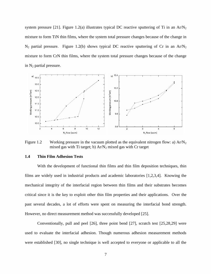
system pressure [21]. Figure 1.2(a) illustrates typical DC reactive sputtering of Ti in an Ar/N2
mixture to form TiN thin films, where the system total pressure changes because of the change in
N2 partial pressure. Figure 1.2(b) shows typical DC reactive sputtering of Cr in an Ar/N2
mixture to form CrN thin films, where the system total pressure changes because of the change
in N2 partial pressure.
Figure 1.2 Working pressure in the vacuum plotted as the equivalent nitrogen flow: a) Ar/N2
mixed gas with Ti target; b) Ar/N2 mixed gas with Cr target
1.4 Thin Film Adhesion Tests
With the development of functional thin films and thin film deposition techniques, thin
films are widely used in industrial products and academic laboratories [1,2,3,4]. Knowing the
mechanical integrity of the interfacial region between thin films and their substrates becomes
critical since it is the key to exploit other thin film properties and their applications. Over the
past several decades, a lot of efforts were spent on measuring the interfacial bond strength.
However, no direct measurement method was successfully developed [25].
Conventionally, pull and peel [26], three point bend [27], scratch test [25,28,29] were
used to evaluate the interfacial adhesion. Though numerous adhesion measurement methods
were established [30], no single technique is well accepted to everyone or applicable to all the
8
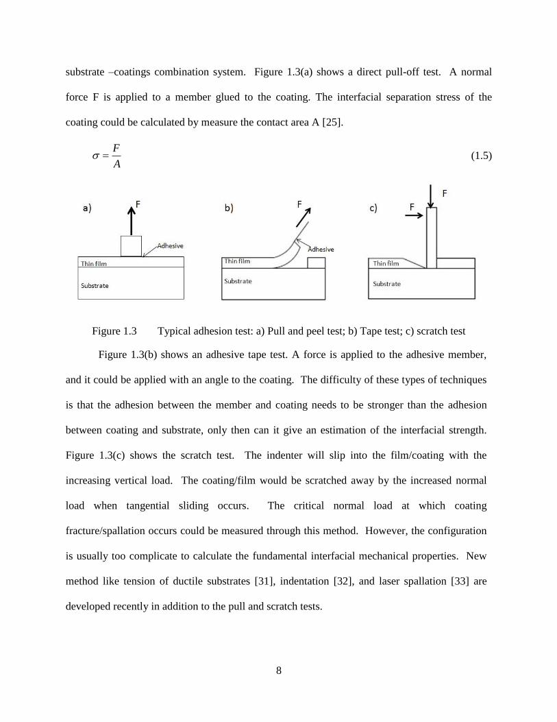
substrate –coatings combination system. Figure 1.3(a) shows a direct pull-off test. A normal
force F is applied to a member glued to the coating. The interfacial separation stress of the
coating could be calculated by measure the contact area A [25].
A
F (1.5)
Figure 1.3 Typical adhesion test: a) Pull and peel test; b) Tape test; c) scratch test
Figure 1.3(b) shows an adhesive tape test. A force is applied to the adhesive member,
and it could be applied with an angle to the coating. The difficulty of these types of techniques
is that the adhesion between the member and coating needs to be stronger than the adhesion
between coating and substrate, only then can it give an estimation of the interfacial strength.
Figure 1.3(c) shows the scratch test. The indenter will slip into the film/coating with the
increasing vertical load. The coating/film would be scratched away by the increased normal
load when tangential sliding occurs. The critical normal load at which coating
fracture/spallation occurs could be measured through this method. However, the configuration
is usually too complicate to calculate the fundamental interfacial mechanical properties. New
method like tension of ductile substrates [31], indentation [32], and laser spallation [33] are
developed recently in addition to the pull and scratch tests.

9
In the laser spallation configuration, a high-fluence laser is travelling toward the
film/substrate region. At the interface, the reflection of the laser-induced strain pulse will
induce the tensile stress which would cause spallation of the coating. From the critical laser
fluence, the interfacial tensile strength could be derived [33].
In the tension test configuration, brittle thin film was deposited onto a ductile substrate.
After the tension load was applied, both the thin film and the substrate experienced the same
strain. The strain will be elastic in the film and plastic in the substrate and induce cracks
generated in the film, which is perpendicular to the tension load direction. When such
transverse cracks occur, further tensile loading of the film occurs through shear of the
film/substrate interfacial region. The transverse crack density in the film will grow until it
reaches a plateau value, at which point the spacing between adjacent cracks will remain roughly
constant without any further decrease as the substrate plastic strain grows beyond this point.
Combine the initial tensile stress at which transverse crack forms in the film and the crack
density at or after the plateau point, an effective interfacial shear strength could be derived [31].
1.5 Size Effect in Thin Film Interlayer
Size effects in plasticity have been documented through many experiments over the past
two decades, including torsion of wires [ 34], bending of beams [ 35 ], and indentation by
pyramidal [36], rectangle strip [37] and diamond wedge [38] indenters. Figure 1.4(a) shows that
the hardness of single crystal Al increases dramatically as the Berkovich indenter diameter
decreases. Size effects were also observed in uniaxial compression tests on cylindrical micro-
pillars cut by focus ion beam (FIB) milling [39]. Figure 1.4(b) shows that the yield strength of
Ni based micro-pillars decreases significantly as the pillar diameter increases.

10
Figure 1.4 Size effect: a) Single crystal Al hardness plotted as the equivalent indenter
diameter [37]; b) Compression stress-strain curve of Ni micropillars in different
diameter [39]
Shear plastic flow in confined thin layers is also of significant interest since it is one of
the typical cases studied in the development of strain gradient plasticity (SGP). According to
SGP, size effects in shear flow of confined thin layers are associated with geometrically
necessary dislocations (GNDs) generated when dislocations are blocked at the interfaces.
Numerous models were used to analyze the mechanical reaction of confined thin films
depending on their thickness [40,41,42,43,44], and they more or less predict similar behaviors.
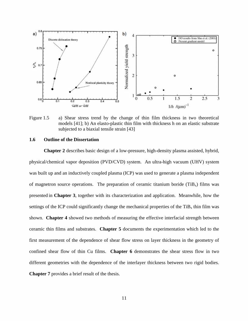
Figure 1.5(a) shows the shear stress trend by the change of the film thickness based on two
theories. Figure 1.5(b) shows the comparison of two gradient theories.
Experimental attempts to measure shear plastic flow in confined thin layers was carried
out by V. Tagraielli and N. Fleck [45]. Thin Al foils of different thicknesses were sandwiched in
between and confined by Al2O3 ceramic layers. Shear loading of the thin Al layers was induced
by tensile loading of Al2O3. However, this experiment yielded no conclusive results due to
experimental difficulties.
11
Figure 1.5 a) Shear stress trend by the change of thin film thickness in two theoretical
models [41]; b) An elasto-plastic thin film with thickness h on an elastic substrate
subjected to a biaxial tensile strain [43]
1.6 Outline of the Dissertation
Chapter 2 describes basic design of a low-pressure, high-density plasma assisted, hybrid,
physical/chemical vapor deposition (PVD/CVD) system. An ultra-high vacuum (UHV) system
was built up and an inductively coupled plasma (ICP) was used to generate a plasma independent
of magnetron source operations. The preparation of ceramic titanium boride (TiBx) films was
presented in Chapter 3, together with its characterization and application. Meanwhile, how the
settings of the ICP could significantly change the mechanical properties of the TiBx thin film was
shown. Chapter 4 showed two methods of measuring the effective interfacial strength between
ceramic thin films and substrates. Chapter 5 documents the experimentation which led to the
first measurement of the dependence of shear flow stress on layer thickness in the geometry of
confined shear flow of thin Cu films. Chapter 6 demonstrates the shear stress flow in two
different geometries with the dependence of the interlayer thickness between two rigid bodies.
Chapter 7 provides a brief result of the thesis.

12
1.7 References
[1] H. A. Tasdemir, M. Wakayama, T. Tokoroyama, H. Kousaka, N. Umehara, Y. Mabuchi,
T. Higuchi, The effect of oil temperature and additive concentration on the wear of non-
hydrogenated DLC coating, Tribology International, Vol 77,Page 65-71 (2014).
[2] A. Ghiotti, S. Bruschi, Tribological Behaviour of DLC coatings for sheet metal forming
tools.
[3] A. Vanhulsel, F. Velasco, R. Jacobs, L. Eersels, D. Havermans, E.W. Roberts, I.
Sherrington, M.J. Anderson, L, Gaillard, DLC solid lubricant coatings on ball bearings
for space application.
[4] Cody H. Nguyen, K. Chandrashekhara, Victor Birman, Multifunctional thermal barrier
coating in aerospace sandwich panels.
[5] K.E. Petersen, Silicon as a mechanical material, Proc. IEEE 70, 420 (1982).
[6] J. Bryzek, Emergence of a $Trillion MEMS sensor market, presentated at the
SensorsTechnology & Application Conference (SensorsCon2012, March 6, 2012, Santa
Clara, California).
[7] J.W. Knutti, H.V. Allen, Trends in MEMS Commercialization, in Advanced Micro and
Nanosystems. Vol. 1, edited by H. Baltes, O. Brand, G. K. Fedder, C. Hierold, J. Korvink,
O. Tabata, WILEY-VCH, Weinheim (2004).
[8] K. Kanda, I. Kanno, H. Kotera, K. Wasa, Simple fabrication of metal-based piezoelectric
MEMS by direct deposition of Pb(Zr, Ti)O3 thin films on titanium substrates, J.
Microelectromechanical Systems 18, 610 (2009).
[9] S. Matsushita, I. Kanno, K. Adachi, R. Yokokawa, H. Kotera, Metal-based piezoelectric
microelectromechanical systems scanner composed of Pb(Zr, Ti)O3 thin film on titanium
substrate, Microsyst. Technol. 18, 765 (2012).
[10] M. Duch, J. Esteve, E. Gomez, R. Perez-Castillejos, E. Valles, Electrodeposited Co-Ni
alloys for MEMS, J. Micromech. Microeng. 12, 400 (2002).
[11] Y. Bellouard, Shape memory alloys for microsystems: A review from a material research
perspective, Mater. Sci. Eng. A481/482, 582 (2008).
[12] T.N. Pornsin-Sirirak, Y.C. Tai, H. Nassef, C.M. Ho, Titanium-alloy MEMS wing
technology for a micro aerial vehicle application, Sensors and Actuators A89, 95 (2001).
[13] M. Geiger, M. Kleiner, R. Eckstein, N. Tiesler, U. Engel, Microforming, CIRP Annals -
Manufacturing Technology 50, 445 (2001).
13
[14] M. Arentoft, R.S. Eriksen, H.N. Hansen, N.A. Paldan, Towards the first generation micro
bulk forming system, CIRP Annals - Manufacturing Technol. 60, 335 (2011).
[15] J.S. Stoelken, A.G. Evans, A microbend test method for measuring the plasticity length
scale, Acta mater. 46, 5109 (1998).
[16] N. Krishnan, J. Cao, K. Dohda, Study of the Size Effects on friction conditions in
microextrusion - Part I: microextrusion experiments and analysis, ASME J.
Manufacturing Sci. Eng. 129, 669 (2007).
[17] W.L. Chan, M.W. Fu, B. Yang, Experimental studies of the size effect affected
microscale plastic deformation in micro upsetting process, Mater. Sci. Eng. A534, 374
(2012).
[18] David S. Rickerby, Allan Matthews, Advanced surface coatings (1991).
[19] W. R. Grove, On the elctro-chemical polarity of gases, Phil. Trans. R. Soc. 142 (1852).
[20] Michael Faraday, The bakerian lecture: Experimenal relations of gold (and other metals)
to light, Phil Trans R Soc 147 (1857).
[21] David A. Glocker, S Ismat Shah, Handbook of thin film process technology (1995).
[22] Milton Ohring, Materials science of thin films, 2nd edition (2002).
[23 ] John E. Harry, Introduction to Plasma Technology (2010).
[24] www.directvacuum.com.
[25] P. A. Stainmann, H. E. Hintermann, A review of the mechanical tests for assessment of
thin-film adhesion, Journals of vacuum science and technology a-Vacuum surfaces and
films, 7 (1989).
[26] Akira Kinbara, Ichiharu Kondo, Adhesion measurement of thin metal films by scratch,
peel, and pull methods, Adhesion measurement of films and coatings, p. 71 (1995).
[27] D. Muller, Y. R. Cho, S. Berg. E. Fromm, Fracture mechanics test for measuring the
adhesion of magnetron-sputtered TiN coatings, Adhesion measurement of films and
coatings, p. 87 (1995).
[28] B. Ollivier, A. Matthews, Adhesion of diamond-like carbon films on polymers: an
assessment of the validity of the scratch test technique applied to flexible substrates,
Adhesion measurement of films and coatings, p. 103 (1995).
14
[29] F. Ramos, M. T. Vieira, Adhesion improvement of RF-sputtered alumina coatings as
determined by the scratch test, Adhesion measurement of films and coatings, p. 115
(1995).
[30] K. L. Mittal (ed), Adhesion measurement of films and coatings (VSP, Utrecht, The
Netherlands, 1, 1995; 2, 2001).
[31] D. C. Agrawal and R. Raj, Measurement of the ultimate shear strength of a metal-ceramic
interface, Acta Metall. 37, 1265 (1989).
[32] M. D. Drory and J. W. Hutchinson, Measurement of the adhesion of brittle films on a
ductile substrate by indentation, Proc. R. Soc. Lond. A452, 2319 (1996).
[33] V. Gupta, V. Kireev, J. Tian, H. Yoshida, H. Akahoshi, Glass-modified stress waves for
adhesion measurement of ultra thin films for device applications, J. Mech. Phys. Solid 51,
1295 (2003).
[34] N.A. Fleck, G.M. Muller, M.F. Ashby, J.W. Hutchinson, Strain gradient plasticity: theory
and experiment, Acta Metall. Mater. 42, 475-487 (1994).
[35] J.S. Stolken, A.G. Evans, A microbend test method for measuring the plasticity length
scale, Acta Mater. 46, 5109–5115 (1998).
[36] Q. Ma, D.R. Clarke, Size dependent hardness of silver single crystals, J. Mater. Res. 10,
853-863 (1995).
[37] Ke Chen, W. J. Meng, Fanghua Mei, J Hiller, D. J. Miller, From micro-to nano scale
molding of metals : size effect during modling of single crystal Al with rectangular strip
punch, Acta Materialia Vol 59 (2011).
[38] Ke Chen, W. J. Meng, G. B. Sinclair, Size dependence of the plane-strain response of
single crystal Al to indentation by diamond wedges, Acta materialia, Vol 60 (2012).
[39] M.D. Uchic, D. M. Dimiduk, J. N. Florando, W. D.Nix, “Sample dimensions influence
strength and crystal plasticity.” Science, 305, p. 986 (2004).
[40] N.A. Fleck, J.W. Hutchinson, Strain gradient plasticity, Adv. Appl. Mech. 33, 295-361
(1997).
[41] J.Y. Shu, N.A. Fleck, E. Van der Giessen, A. Needleman, Boundary layers in constrained
plastic flow: comparison of nonlocal and discrete dislocation plasticity, J. Mech. Phys.
Solids 49, 1361-1395 (2001).
[42] E. Bittencourt, A. Needleman, M.E. Gurtin, E. Van der Giessen, A comparison of
nonlocal continuum and discrete dislocation plasticity predictions, J. Mech. Phys. Solids
51(2), 281-310 (2003).

15
[43] P. Fredriksson, P. Gudmundson, Size-dependent yield strength of thin films, Int. J.
Plasticity 21(9), 1834-1854 (2005).
[44] S.P. Lele, L. Anand, A small-deformation strain-gradient theory for isotropic viscoplastic
materials, Phil. Mag. 88(30-32), 3655-3689 (2008).
[45] V.L. Tagarielli, N.A. Fleck, The shear response of a thin aluminum layer, J. Appl. Mech.
78, 014505/1-3 (2011).
16
CHAPTER 2
DESIGN AND CONSTRUCTION OF A HIGH-DENSITY PLASMA ASSISTED ULTRA
HIGH VACUUM (UHV) PHYSICAL VAPOR DEPOSITION (PVD) SYSTEM
As a part of work performed during this dissertation study, a previously existing plasma
assisted vapor deposition system was modified and updated. The updated system enables the
deposition chamber to be maintained under ultra-high vacuum (UHV) conditions at all times,
with sample transfer from a load lock chamber to the deposition chamber occurring under high
vacuum conditions. In what follows, details of system design and construction are given.
2.1 Vacuum System
The entire deposition system is equipped with two turbo molecular pumps, one cryogenic
pump, one ion pump, two ion gauges (IG), one residual gas analyzer (RGA), a heatable sample
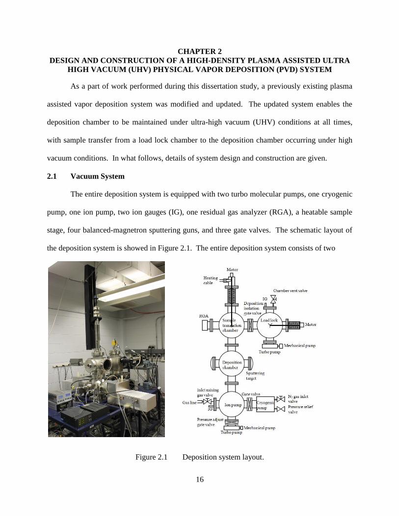
stage, four balanced-magnetron sputtering guns, and three gate valves. The schematic layout of
the deposition system is showed in Figure 2.1. The entire deposition system consists of two
Figure 2.1 Deposition system layout.

17
sections separated by a gate valve: a sample load lock section to load/unload samples and a
deposition section maintained under UHV conditions at all times [1].
The load lock chamber is pumped by a turbo molecular pump (Pfeiffer, N2 pumping
speed 67liter/s) backed by a rotary mechanical pump (Pheiffer, N2 pumping speed 5m3/hr). Once
a cleaned sample is loaded into the chamber, it usually takes about 6 hours to reach the target
vacuum level of ~1 × 10⁻⁶
Torr. The deposition chamber is pumped by a combination of pumps:
1) a turbo molecular pump (Pfeiffer, N2 pumping speed 260liter/s) backed by a rotary
mechanical pump (Pfeiffer, N2 pumping speed 6m3/hr), 2) a sputter ion pump (Gamma Vacuum,
N2 pumping speed 40-75liter/s), and 3) a cryogenic pump (Sumitomo, air pumping speed
1500liter/s). A RF quadrupole mass spectrometer (RGA, Stanford Research Systems) is used to
measure the residual gas content in the deposition chamber, assess whether all pumps are under
proper working conditions, and monitor gaseous impurities within the deposition system and
possible system leakage. The entire deposition system is sealed with Conflat type Cu gaskets
and Viton O-rings. In addition, all the gas lines are sealed with VCR type Ni gaskets.
The entire deposition system is fully sealed, together with the pumping system, RGA, and
ion gauge. It is first pumped down by the turbo molecular pump, which is backed up by the
connecting rotary mechanical pump [ 2 ]. This set up reduces the back-streaming of the
mechanical pump oil. As soon as the pump system starts to work, heating tapes wrapped around
the outside of the chamber shell help heat up the entire system. The chamber wall temperature
reaches ~100°C after an hour. As a result of this baking, gases previously trapped onto the inner
walls of the chamber are gradually released. A 48-hour or longer baking process is needed to
achieve an ideal base pressure of 3-5 × 10⁻⁹
Torr, with the help of the cryogenic and ion pumps.
Typical RGA graphs displayed in Figure 2.2(a), (b), (c) show the gaseous content left in the
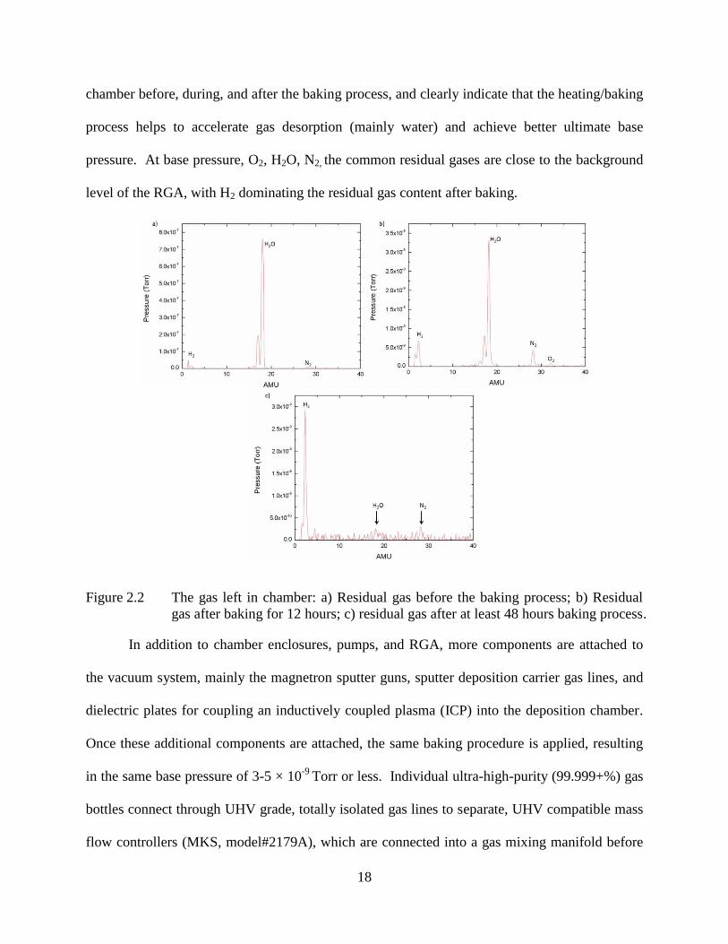
18
chamber before, during, and after the baking process, and clearly indicate that the heating/baking
process helps to accelerate gas desorption (mainly water) and achieve better ultimate base
pressure. At base pressure, O2, H2O, N2, the common residual gases are close to the background
level of the RGA, with H2 dominating the residual gas content after baking.
Figure 2.2 The gas left in chamber: a) Residual gas before the baking process; b) Residual
gas after baking for 12 hours; c) residual gas after at least 48 hours baking process.
In addition to chamber enclosures, pumps, and RGA, more components are attached to
the vacuum system, mainly the magnetron sputter guns, sputter deposition carrier gas lines, and
dielectric plates for coupling an inductively coupled plasma (ICP) into the deposition chamber.
Once these additional components are attached, the same baking procedure is applied, resulting
in the same base pressure of 3-5 × 10⁻⁹
Torr or less. Individual ultra-high-purity (99.999+%) gas
bottles connect through UHV grade, totally isolated gas lines to separate, UHV compatible mass
flow controllers (MKS, model#2179A), which are connected into a gas mixing manifold before
19
introduction into the deposition chamber. The two mostly commonly used gases for this
dissertation work are Ar and N2.
The manually operated gate valve between the turbo molecular pump and the deposition
chamber is used to adjust the effective pumping speed and consequently the total pressure within
the deposition chamber during the deposition process. The gate valve between the cryogenic
pump and the deposition chamber is used to isolate the cryogenic pump from the input gas
stream during the deposition process.
2.2 Sample Transfer Mechanism
A sample holder and sample transfer system, shown in Figure 2.3(a), are custom designed
for thin film deposition onto two-inch diameter Si wafers with/without substrate heating. The
round-shaped sample holder has a clearance hole in the center, into which cleaned Si wafers will
be placed. For ease of Si wafer placement, the clearance hole has a crater rim with a diameter
slightly larger than two-inch and a depth slightly larger than the thickness of typical Si wafers. A
wafer is held in place by another stainless steel holding ring, with a clearance hole of one-inch
diameter in the center. This holding ring is held onto the sample holder by screws. This design
creates a cavity-like placement for the Si wafer, designed for a more even temperature
distribution on the wafer in case it is heated up during deposition.
Three set screws and three L-shape openings are evenly distributed on the sidewall of the
sample holder. This sample holder will be first loaded onto the load lock transfer piece (after the
Si wafer is loaded), which has three evenly distributed arms. This transfer piece is connected to
the stainless steel rod manipulator housed within the load lock chamber, and could move
horizontally. On each arm, it has an “L-shape” opening, compatible with every set screw on the
sample holder. With this “set screw-L shape” mechanism, the sample holder could be attached to
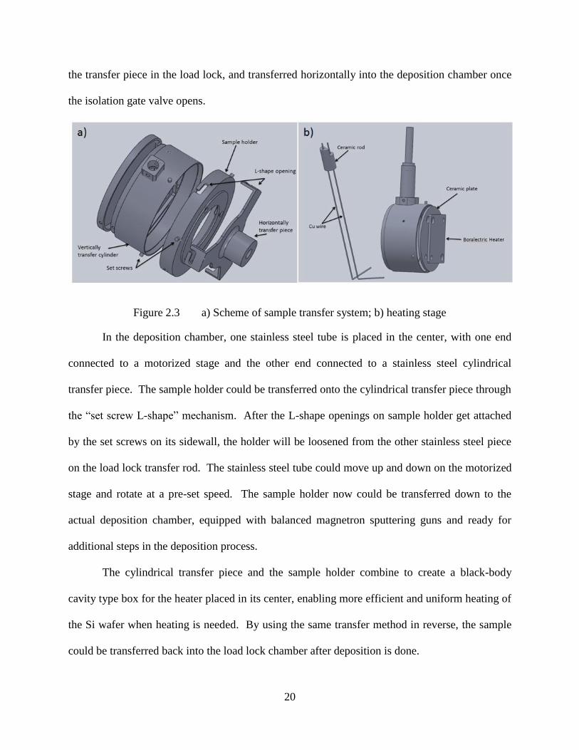
20
the transfer piece in the load lock, and transferred horizontally into the deposition chamber once
the isolation gate valve opens.
Figure 2.3 a) Scheme of sample transfer system; b) heating stage
In the deposition chamber, one stainless steel tube is placed in the center, with one end
connected to a motorized stage and the other end connected to a stainless steel cylindrical
transfer piece. The sample holder could be transferred onto the cylindrical transfer piece through
the “set screw L-shape” mechanism. After the L-shape openings on sample holder get attached
by the set screws on its sidewall, the holder will be loosened from the other stainless steel piece
on the load lock transfer rod. The stainless steel tube could move up and down on the motorized
stage and rotate at a pre-set speed. The sample holder now could be transferred down to the
actual deposition chamber, equipped with balanced magnetron sputtering guns and ready for
additional steps in the deposition process.
The cylindrical transfer piece and the sample holder combine to create a black-body
cavity type box for the heater placed in its center, enabling more efficient and uniform heating of
the Si wafer when heating is needed. By using the same transfer method in reverse, the sample
could be transferred back into the load lock chamber after deposition is done.

21
2.3 Heating Stage
A BORALECTRIC heater (Momentive Performance) is used as the heating source in
this vacuum system. Figure 2.3(b) shows the heating stage in detail. The heater is connected to
the L-shaped Cu wire through a round-shaped quarter-inch thick ceramic plate (used for isolation
and fixing the heater in position) by stainless steel screw, and isolated to this ceramic plate by
wrapping another ceramic tube outside the screw. The two Cu wires, supplying the necessary
electric current to heat up the Boralectric heater, go up to the stainless steel tube attached on the
top of the cylindrical transfer piece, and go through the ceramic tube pre-installed in the stainless
steel tube. This will keep the two Cu wires in position and separated from each other. On the
other end of the two Cu wires are electric cables covered with glass fiber. These two cables will
be connected to the ceramic-metal feed-through that provides the DC power from outside the
vacuum system. This heater stage circuit will tremendously reduce the possibility of electrical
shorts when bias voltages are applied to the sample holder while the sample heater is working.
2.4 Thin Film Deposition
Figure 2.4 shows a schematic of typical plasma assisted thin film deposition. Planar Cu
induction coils are placed on the vacuum exterior side close to two parallel quartz windows on
the deposition chamber. The two windows serve as the dielectric plates through which inductive
coupling occurs between the external Cu coils and the ICP inside the deposition chamber [3].
Each Cu coil is connected to a 13.56 MHz RF power supply, through a commercial auto-tuning
network. Four DC magnetron sputtering guns are placed with a 60-deg orientation to the
inductively coupled plasma column. The electrically isolated sample holder is placed at the
center of the deposition chamber, and could be rotated as a fixed rate or placed at a stationary
position facing one or more sputter targets. An independently controlled bias voltage could be
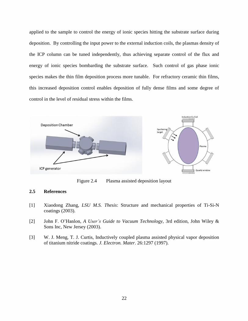
22
applied to the sample to control the energy of ionic species hitting the substrate surface during
deposition. By controlling the input power to the external induction coils, the plasmas density of
the ICP column can be tuned independently, thus achieving separate control of the flux and
energy of ionic species bombarding the substrate surface. Such control of gas phase ionic
species makes the thin film deposition process more tunable. For refractory ceramic thin films,
this increased deposition control enables deposition of fully dense films and some degree of
control in the level of residual stress within the films.
Figure 2.4 Plasma assisted deposition layout
2.5 References
[1] Xiaodong Zhang, LSU M.S. Thesis: Structure and mechanical properties of Ti-Si-N
coatings (2003).
[2] John F. O’Hanlon, A User’s Guide to Vacuum Technology, 3rd edition, John Wiley &
Sons Inc, New Jersey (2003).
[3] W. J. Meng, T. J. Curtis, Inductively coupled plasma assisted physical vapor deposition
of titanium nitride coatings. J. Electron. Mater. 26:1297 (1997).
23
CHAPTER 3
LOW TEMPERATURE DEPOSITED TITANIUM BORIDE THIN FILMS
AND THEIR APPLCATION TO SURFACE ENGINEERING OF MICROSCALE MOLD
INSERT
3.1 Introduction
Direct replication of microscale structures in metals by compression molding using
microscale mold inserts is a promising technique for low-cost, high-throughput, fabrication of
metal-based microdevices [1]. Extensive plastic flow during micromolding brings fresh metal-
to-metal contact between the mold insert and the molded material. This contact can cause
chemical reactions between the insert and the molded metal, leading to damage of molded parts
and failure of the mold insert. Engineering the near-surface chemical and tribological properties
of mold inserts is critical to alleviate such damage and improve insert life. Depositing suitable
ceramic thin films conformally onto mold inserts with non-planar microscale features has been
shown to be a feasible avenue for engineering surfaces of microscale mold inserts [2,3], and has
led to demonstrations of compression micromolding of a wide range of metals and alloys,
including Al [4], Cu [5], Ni [6], and NiTi [7].
Elemental Al and Al alloys possess good thermal conductivity and are relatively
inexpensive. Microscale structures made of Al and Al alloys are of particular interest as building
blocks for metal-based microchannel heat exchangers [8]. Although successful Al micromolding
was demonstrated with mold inserts deposited with a conformal, amorphous hydrogenated
carbon (a-C:H) based coating layer [4], the degradation of a-C:H films at medium temperatures
of 300-500 °C [9,10] limits their long term stability and consequently life of a-C:H coated mold
inserts. Thin films of titanium diboride (TiB2) have been deposited by different vapor phase
deposition techniques: chemical vapor deposition (CVD) at temperatures >900 °C from gaseous
TiCl4, BCl3, andB2H6 precursors [11,12]; glow-discharge assisted CVD at 480-650 °C from
24
gaseous TiCl4 and BCl3 precursors [13]; inductively coupled plasma (ICP) assisted CVD at 250-
400 °C from gaseous mixtures of TiCl4, BCl3, H2, and Ar [14]; triode magnetron sputtering of
TiB2 targets at ~450°C [26]; unbalanced magnetron sputtering at 300 °C from stoichiometric
TiB2 targets [15]. Thin films of TiB2 are known for high chemical stability, and show promise
for Al dry machining applications [16,17].
In this paper, we report low temperature deposition of titanium boride (TiBx) thin films
by balanced magnetron sputtering in Ar and ICP assisted balanced magnetron sputtering in Ar
from stoichiometric TiB2 targets. Chemical, morphological, structural, and mechanical
characterizations of deposited TiBx films were carried out with X-ray photoelectron
spectroscopy (XPS), scanning electron microscopy (SEM), transmission electron microscopy
(TEM), and instrumented nanoindentation. TiBx thin films deposited at lower plasma densities
via balanced magnetron sputtering were contrasted to those deposited at much higher plasma
densities due to the ICP assist. The potential of applying TiBx thin films conformally deposited
onto non-planar mold inserts to microscale compression molding of Al was explored. Fully
dense TiBx thin films deposited conformally onto microscale Ta inserts are shown to withstand
repeated contact with Al at molding temperatures of ~450 °C without delamination, and
therefore of potential use for engineering insert surfaces for Al micromolding.
3.2 Experimental Procedures
Deposition of TiBx films was carried out in an ultra high vacuum physical/chemical
vapor deposition (PVD/CVD) tool. This tool housed a 13.56 MHz ICP and four balanced
magnetron sputtering sources. The ICP and the sputtering sources could be operated
independently [18,19]. A schematic of the deposition chamber is shown in Figure 3.1, which
had a base pressure of < 4×10⁻⁷
Pa. Cleaned substrates were first loaded into a load lock
25
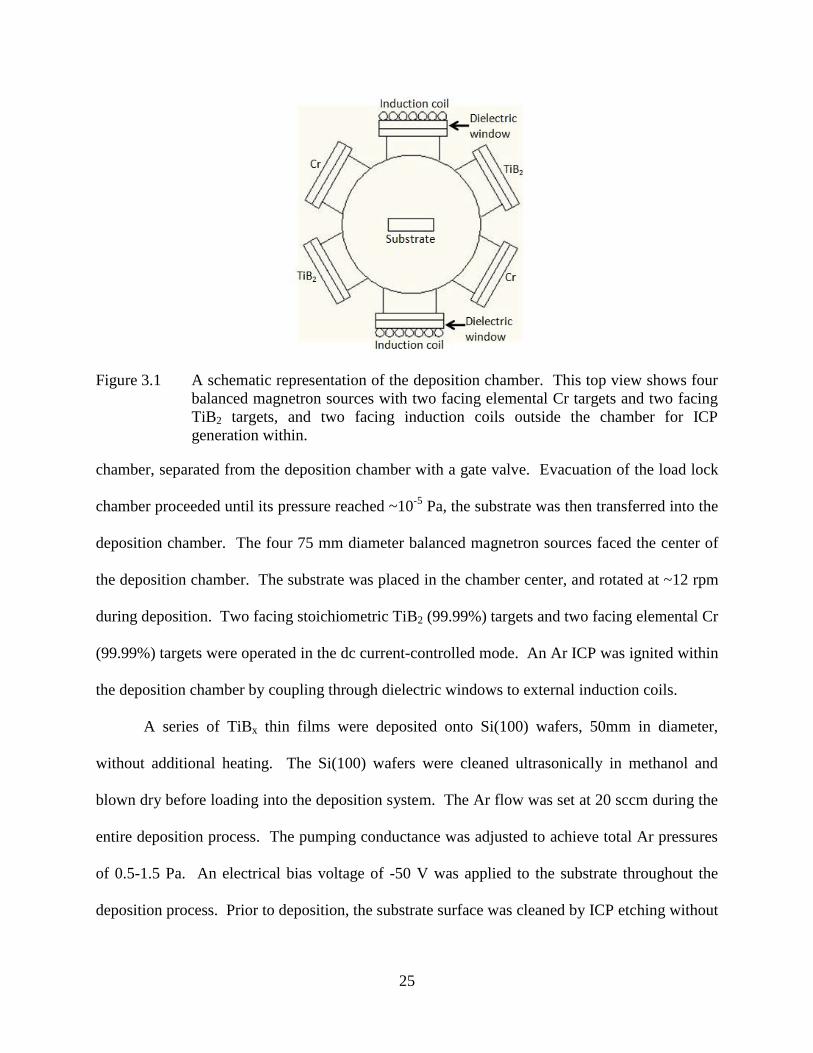
Figure 3.1 A schematic representation of the deposition chamber. This top view shows four
balanced magnetron sources with two facing elemental Cr targets and two facing
TiB2 targets, and two facing induction coils outside the chamber for ICP
generation within.
chamber, separated from the deposition chamber with a gate valve. Evacuation of the load lock
chamber proceeded until its pressure reached ~10-5
Pa, the substrate was then transferred into the
deposition chamber. The four 75 mm diameter balanced magnetron sources faced the center of
the deposition chamber. The substrate was placed in the chamber center, and rotated at ~12 rpm
during deposition. Two facing stoichiometric TiB2 (99.99%) targets and two facing elemental Cr
(99.99%) targets were operated in the dc current-controlled mode. An Ar ICP was ignited within
the deposition chamber by coupling through dielectric windows to external induction coils.
A series of TiBx thin films were deposited onto Si(100) wafers, 50mm in diameter,
without additional heating. The Si(100) wafers were cleaned ultrasonically in methanol and
blown dry before loading into the deposition system. The Ar flow was set at 20 sccm during the
entire deposition process. The pumping conductance was adjusted to achieve total Ar pressures
of 0.5-1.5 Pa. An electrical bias voltage of -50 V was applied to the substrate throughout the
deposition process. Prior to deposition, the substrate surface was cleaned by ICP etching without
26
energizing the TiB2 and Cr targets. The total input power to the ICP induction coils was 1000 W
during etching, divided equally between the two coils.
After plasma etching, a Cr interlayer was immediately deposited onto the substrate by
balanced magnetron sputtering of the two Cr targets without ICP assist. During Cr deposition,
the two facing Cr targets were operated at 1.0 A. The deposition of a TiBx top layer commenced
immediately after Cr interlayer deposition. Balanced magnetron sputtering of the two facing
TiB2 targets was conducted with and without ICP assist. During TiBx deposition, the two facing
TiB2 targets were operated at 0.5 A. With ICP assist, the total input power to the ICP induction
coils was set at 1000 W, divided equally between the two coils. Without ICP assist, the total ICP
input power was set to zero. Minor variations of deposition parameters were made, such as the
total Ar pressure, the Cr interlayer thickness, or the TiBx layer thickness. Table 3.1 lists the
deposition parameters for a number of TiBx/Cr/Si(100) specimens, and illustrates such minor
deposition parameter variations. It was found that such minor variations did not yield any
significant difference in the resulting films.
The TiB2 target power density was estimated from the total target power during
sputtering together with an estimation of the area of the balanced magnetron race track on the
target, and was determined to be ~100W/cm2 with or without ICP assist. Previous measurements
of plasma potential and ion current density within the ICP assisted CVD/PVD environment were
performed using an electron emissive wire probe and a conventional planar Langmuir disk probe
[20]. The densities of the low-pressure quasi-neutral plasmas were calculated from data on
measured ion current densities [21]. The addition of the ICP raises the plasma density within the
deposition chamber to ~1011
cm-3
, at least one order of magnitude higher as compared to the case
of balanced magnetron sputtering without ICP assist [20]. The plasma present near the substrate

27
Table 3.1 Conditions for deposition of a series of TiB2/Cr/Si(100) specimens
Run Substrate etching Cr interlayer TiB2 top layer
Substrate
bias (V)
Ar
pressure
(Pa)
ICP input
power
(W)
Time
(min)
ICP input
power
(W)
Time
(min)
ICP input
power
(W)
Time
(min)
1
-50
1.33
1000
5
0
10 1000 60
2 0.67 5 1000 60
3 0.67 5 0 45
4 0.67 10 0 45
surface during deposition causes a rise in substrate temperature, even without additional
substrate heating. Previous substrate temperature measurements during deposition showed
substrate temperatures of ~210 °C during etching, of ~140 °C during deposition without ICP
assist, and of ~225 °C during ICP assisted balanced magnetron sputter deposition [20,22]. The
TiBx deposition rates were respectively ~220nm/60min and ~360nm/60min with or without ICP
assist, or ~0.6 Å/s to ~1.0 Å/s. The lower TiBx deposition rate with ICP assist is consistent with
increasing ion bombardment of the growth surface during deposition.
Chemical characterization of as-deposited TiBx/Cr/Si(100) specimens was carried out
with XPS on a Kratos AXIS165 system, using a monochromatic Al Kα excitation source. All
XPS spectra were collected after specimen surface sputter cleaning using a 5 kV Ar+ ion gun
operated at a total output current of 15 mA. The duration for cleaning was determined such that
no perceptible change in XPS spectral features could be affected through further sputtering, and
ranged from ~10 min to ~100 min. Chemical compositions were obtained from raw XPS spectra
using Kratos supplied sensitivity factors.
28
The surface and cross-sectional morphology of as-deposited TiBx/Cr/Si(100) specimens
were examined on a FEI Quanta3D FEG electron column/focused Ga+ ion beam column dual-
beam instrument (FIB). Cross-sectional transmission electron microscopy (TEM) studies of
TiBx/Cr/Si(100) specimens were carried out on a JOEL JEM2011 microscope operated at 200
kV. Cross-sectional TEM specimens were prepared by FIB ion beam cutting followed by lift-out
with an OmniProbe W probe installed within the FIB instrument, and thinned to electron
transparency using 30 kV Ga+ ion beams with successively decreasing currents. Additional SEM
examinations were performed on a Hitachi S3600N microscope.
Instrumented nanoindentation of as-deposited TiBx/Cr/Si(100) specimens was carried out
on a MTS Nanoindenter XP System. A Berkovich diamond indenter was used. Calibration of
the instrument load frame stiffness and the indenter tip area function were determined with a
factory-supplied fused silica specimen. A range of calibration loads were applied, ranging from
~4×101 to ~4×10
4 μN, corresponding to an indenter contact depth (hc) range from ~10 to 590 nm.
Several indents were conducted at each load. Indentations on TiBx/Cr/Si(100) specimens were
carried out at multiple loads, ranging from ~160 to ~40960 μN, with multiple indents performed
at each load. Values of the indentation modulus, Eind=E/(1-2) where E and are respectively
the Young’s modulus and the Poisson’s ratio, and the hardness, H, were obtained from
experimental load vs. displacement curves.
TiBx thin films were deposited onto non-planar Ta mold inserts following deposition
procedures outlined above, with ICP assist. These Ta inserts consisted of a series of parallel
microscale rectangular protrusions, fabricated on the surface of a flat Ta coupon via micro
electrical discharge machining (EDM). As-machined Ta inserts were subjected to
electrochemical polishing (ECP) to remove an altered surface layer due to the EDM process.
29
Further details on fabrication of the Ta inserts were presented elsewhere [5]. Surfaces of Ta
inserts were etched with an Ar ICP. An elemental Cr interlayer was deposited onto the Ta inserts
immediately after the surface etch. Deposition of the TiBx top layer, typically with a duration of
~75 min, followed immediately after the Cr interlayer deposition with ICP assist.
3.3 Results and Discussion
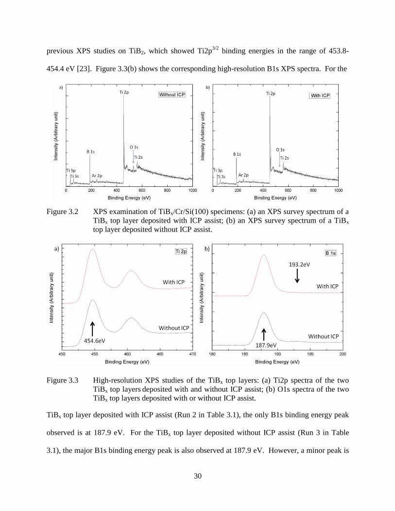
Figure 3.2 shows typical XPS survey spectra collected from the top layers of
TiBx/Cr/Si(100) specimens. Signals from Ti2s, Ti2p, Ti3s, Ti3p, B1s, and Ar2p levels are
clearly visible. To remove oxygen surface contamination due to specimen handling in air, Ar+
ion sputter cleaning of the specimen surfaces was carried out in-situ the XPS analysis chamber.
For the specimen deposited with ICP assist, Run 2 in Table 3.1, 25min of sputter cleaning
removed all of the oxygen signature in the XPS survey spectrum, as shown in Figure 3.2(a), such
that the O1s signal is at the background level. Figure 3.2(b) shows, in contrast, a clear O1s
signal persisting in the XPS survey spectrum of the specimen deposited without ICP assist, Run
3 in Table 3.1, even after ~100min of sputter cleaning. XPS data on this TiBx layer after
prolonged sputter cleaning suggest that, in addition to surface contamination, oxygen was
incorporated into the bulk of this TiBx layer. The overall compositions of the TiBx top layers
shown in Figure 3.2(a) and 3.2(b) were determined as ~Ti26B74, exhibiting no significant
difference whether ICP assist was employed during deposition. Thus XPS data show that the
TiBx top layer is over-stoichiometric with respect to TiB2, with x close to 3.
Figure 3.3(a) shows the corresponding high-resolution Ti2p XPS spectra collected from
two TiBx top layers, deposited with ICP assist (Run 2 in Table 3.1) and without ICP assist (Run 3
in Table 3.1). Measured Ti2p3/2
binding energies from the TiBx top layers are 454.6 eV,
independent of whether the ICP assist was employed during deposition and consistent with
30
previous XPS studies on TiB2, which showed Ti2p3/2
binding energies in the range of 453.8-
454.4 eV [23]. Figure 3.3(b) shows the corresponding high-resolution B1s XPS spectra. For the
Figure 3.2 XPS examination of TiBx/Cr/Si(100) specimens: (a) an XPS survey spectrum of a
TiBx top layer deposited with ICP assist; (b) an XPS survey spectrum of a TiBx
top layer deposited without ICP assist.
Figure 3.3 High-resolution XPS studies of the TiBx top layers: (a) Ti2p spectra of the two
TiBx top layers deposited with and without ICP assist; (b) O1s spectra of the two
TiBx top layers deposited with or without ICP assist.
TiBx top layer deposited with ICP assist (Run 2 in Table 3.1), the only B1s binding energy peak
observed is at 187.9 eV. For the TiBx top layer deposited without ICP assist (Run 3 in Table
3.1), the major B1s binding energy peak is also observed at 187.9 eV. However, a minor peak is
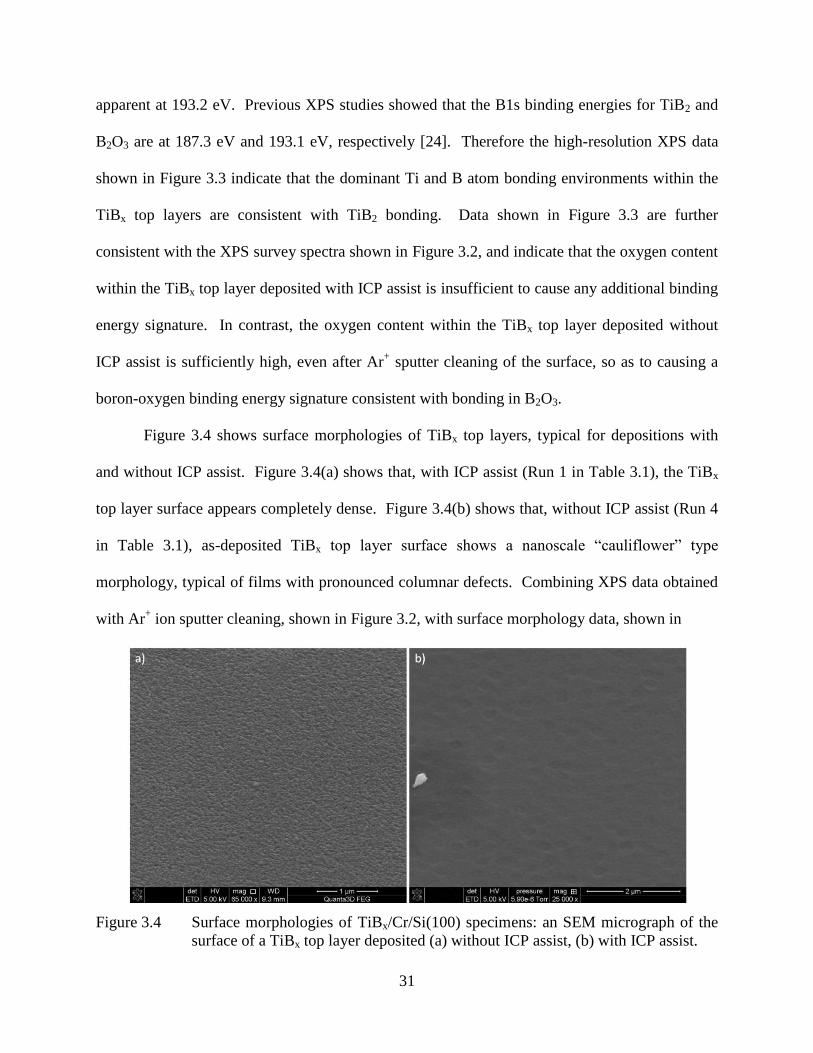
31
apparent at 193.2 eV. Previous XPS studies showed that the B1s binding energies for TiB2 and
B2O3 are at 187.3 eV and 193.1 eV, respectively [24]. Therefore the high-resolution XPS data
shown in Figure 3.3 indicate that the dominant Ti and B atom bonding environments within the
TiBx top layers are consistent with TiB2 bonding. Data shown in Figure 3.3 are further
consistent with the XPS survey spectra shown in Figure 3.2, and indicate that the oxygen content
within the TiBx top layer deposited with ICP assist is insufficient to cause any additional binding
energy signature. In contrast, the oxygen content within the TiBx top layer deposited without
ICP assist is sufficiently high, even after Ar+ sputter cleaning of the surface, so as to causing a
boron-oxygen binding energy signature consistent with bonding in B2O3.
Figure 3.4 shows surface morphologies of TiBx top layers, typical for depositions with
and without ICP assist. Figure 3.4(a) shows that, with ICP assist (Run 1 in Table 3.1), the TiBx
top layer surface appears completely dense. Figure 3.4(b) shows that, without ICP assist (Run 4
in Table 3.1), as-deposited TiBx top layer surface shows a nanoscale “cauliflower” type
morphology, typical of films with pronounced columnar defects. Combining XPS data obtained
with Ar+ ion sputter cleaning, shown in Figure 3.2, with surface morphology data, shown in
Figure 3.4 Surface morphologies of TiBx/Cr/Si(100) specimens: an SEM micrograph of the
surface of a TiBx top layer deposited (a) without ICP assist, (b) with ICP assist.
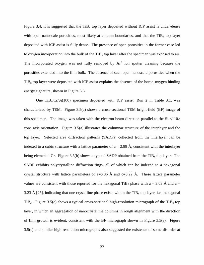
32
Figure 3.4, it is suggested that the TiBx top layer deposited without ICP assist is under-dense
with open nanoscale porosities, most likely at column boundaries, and that the TiBx top layer
deposited with ICP assist is fully dense. The presence of open porosities in the former case led
to oxygen incorporation into the bulk of the TiBx top layer after the specimen was exposed to air.
The incorporated oxygen was not fully removed by Ar+ ion sputter cleaning because the
porosities extended into the film bulk. The absence of such open nanoscale porosities when the
TiBx top layer were deposited with ICP assist explains the absence of the boron-oxygen binding
energy signature, shown in Figure 3.3.
One TiBx/Cr/Si(100) specimen deposited with ICP assist, Run 2 in Table 3.1, was
characterized by TEM. Figure 3.5(a) shows a cross-sectional TEM bright-field (BF) image of
this specimen. The image was taken with the electron beam direction parallel to the Si <110>
zone axis orientation. Figure 3.5(a) illustrates the columnar structure of the interlayer and the
top layer. Selected area diffraction patterns (SADPs) collected from the interlayer can be
indexed to a cubic structure with a lattice parameter of a = 2.88 Å, consistent with the interlayer
being elemental Cr. Figure 3.5(b) shows a typical SADP obtained from the TiBx top layer. The
SADP exhibits polycrystalline diffraction rings, all of which can be indexed to a hexagonal
crystal structure with lattice parameters of a=3.06 Å and c=3.22 Å. These lattice parameter
values are consistent with those reported for the hexagonal TiB2 phase with a = 3.03 Å and c =
3.23 Å [25], indicating that one crystalline phase exists within the TiBx top layer, i.e., hexagonal
TiB2. Figure 3.5(c) shows a typical cross-sectional high-resolution micrograph of the TiBx top
layer, in which an aggregation of nanocrystalline columns in rough alignment with the direction
of film growth is evident, consistent with the BF micrograph shown in Figure 3.5(a). Figure
3.5(c) and similar high-resolution micrographs also suggested the existence of some disorder at
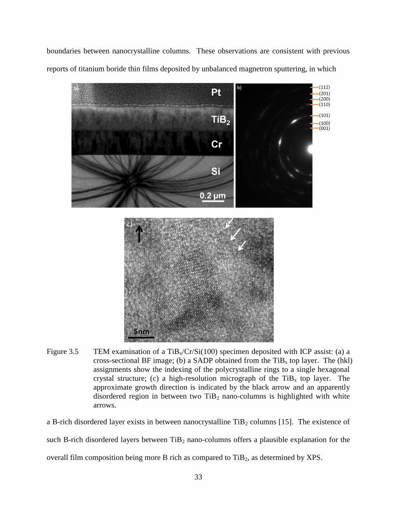
33
boundaries between nanocrystalline columns. These observations are consistent with previous
reports of titanium boride thin films deposited by unbalanced magnetron sputtering, in which
Figure 3.5 TEM examination of a TiBx/Cr/Si(100) specimen deposited with ICP assist: (a) a
cross-sectional BF image; (b) a SADP obtained from the TiBx top layer. The (hkl)
assignments show the indexing of the polycrystalline rings to a single hexagonal
crystal structure; (c) a high-resolution micrograph of the TiBx top layer. The
approximate growth direction is indicated by the black arrow and an apparently
disordered region in between two TiB2 nano-columns is highlighted with white
arrows.
a B-rich disordered layer exists in between nanocrystalline TiB2 columns [15]. The existence of
such B-rich disordered layers between TiB2 nano-columns offers a plausible explanation for the
overall film composition being more B rich as compared to TiB2, as determined by XPS.
34
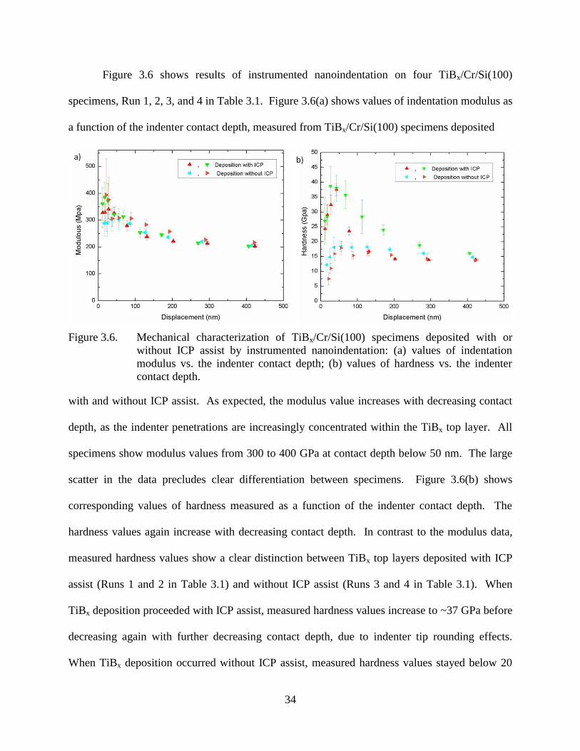
Figure 3.6 shows results of instrumented nanoindentation on four TiBx/Cr/Si(100)
specimens, Run 1, 2, 3, and 4 in Table 3.1. Figure 3.6(a) shows values of indentation modulus as
a function of the indenter contact depth, measured from TiBx/Cr/Si(100) specimens deposited
Figure 3.6. Mechanical characterization of TiBx/Cr/Si(100) specimens deposited with or
without ICP assist by instrumented nanoindentation: (a) values of indentation
modulus vs. the indenter contact depth; (b) values of hardness vs. the indenter
contact depth.
with and without ICP assist. As expected, the modulus value increases with decreasing contact
depth, as the indenter penetrations are increasingly concentrated within the TiBx top layer. All
specimens show modulus values from 300 to 400 GPa at contact depth below 50 nm. The large
scatter in the data precludes clear differentiation between specimens. Figure 3.6(b) shows
corresponding values of hardness measured as a function of the indenter contact depth. The
hardness values again increase with decreasing contact depth. In contrast to the modulus data,
measured hardness values show a clear distinction between TiBx top layers deposited with ICP
assist (Runs 1 and 2 in Table 3.1) and without ICP assist (Runs 3 and 4 in Table 3.1). When
TiBx deposition proceeded with ICP assist, measured hardness values increase to ~37 GPa before
decreasing again with further decreasing contact depth, due to indenter tip rounding effects.
When TiBx deposition occurred without ICP assist, measured hardness values stayed below 20
35
GPa. Indentation results presented in Figure 3.6 are consistent with the suggestion that TiBx
layers deposited without ICP assist are under-dense with open nanoscale porosities at column
boundaries. The increased Ar+ ion bombardment of the substrate surface during ICP assisted
deposition, afforded by the increased plasma density, facilitated further densification of the TiBx
layers and raising their hardness. Refractory ceramics, such as TiB2, are associated with strong
bonding and reduced surface mobilities. The reduced surface mobility in turn leads to difficulty
in film densification duration vapor phase deposition, a difficulty often overcome by going to
higher deposition temperatures [11,12,13,14, 26 ]. It has been shown previously that full
densification of TiN thin films can be affected by increased low energy ion bombardment during
deposition, even at cryogenic temperatures [27]. The present observation of significant increase
in TiBx hardness due to increased Ar+ ion bombardment during low temperature deposition is
consistent with the previous work on TiN deposition.
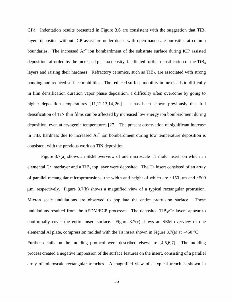
Figure 3.7(a) shows an SEM overview of one microscale Ta mold insert, on which an
elemental Cr interlayer and a TiBx top layer were deposited. The Ta insert consisted of an array
of parallel rectangular microprotrusions, the width and height of which are ~150 m and ~500
m, respectively. Figure 3.7(b) shows a magnified view of a typical rectangular protrusion.
Micron scale undulations are observed to populate the entire protrusion surface. These
undulations resulted from the EDM/ECP processes. The deposited TiBx/Cr layers appear to
conformally cover the entire insert surface. Figure 3.7(c) shows an SEM overview of one
elemental Al plate, compression molded with the Ta insert shown in Figure 3.7(a) at ~450 °C.
Further details on the molding protocol were described elsewhere [4,5,6,7]. The molding
process created a negative impression of the surface features on the insert, consisting of a parallel
array of microscale rectangular trenches. A magnified view of a typical trench is shown in
36
Figure 3.7(d). The trench had near-vertical sidewalls and sharp sidewall-to-bottom transitions.
The undulations on the trench bottom were a negative of those present on the top surface of the
rectangular microprotrusions on the insert. The sidewall surfaces consisted of vertical marks,
resulting from the insert sinking into and pulling out of the molded Al plate during the molding
and demolding processes, respectively. The depth of the molded trenches was determined to be
~300 m. Results presented in Figure 3.7 demonstrate that Ta inserts with conformally
deposited TiBx/Cr layers can be used for microscale compression molding of Al, resulting in
Figure 3.7 A Ta mold insert and a molded Al plate: (a) an SEM overview of a portion of one
Ta insert with TiBx/Cr layers conformally deposited over it; (b) the typical
sidewall surface morphology of rectangle protrusions on the insert; (c) an SEM
overview of an Al plate compression molded by the insert; (d) a magnified view
of a typical molded trench on the Al plate.

37
creation of well- defined microscale features in Al plates in a parallel manner. Figure 3.8(a)
shows an SEM overview of the same Ta insert after Al molding. The shape and surface
Figure 3.8 SEM examination of the Ta insert after Al molding: (a) an SEM overview of the
Ta insert after Al molding; (b) a typical view of sidewall surfaces of rectangle
protrusions on the insert after Al molding. The band on the protrusion sidewall
where transferred Al is present is delineated by the double arrow.
morphology of the insert appeared to be well maintained and not altered by the molding process.
Figure 3.8(b) shows a magnified view of a typical rectangular microprotrusion on the insert
surface. It is apparent from Figure 3.8(b) that the molding and demolding processes led to
material transfer from the molding Al plate to sidewall surfaces of the protrusion. Al transferred
predominantly onto the protrusion sidewall surface, starting from just below the protrusion top
surface to sidewall transition and ending at where contact between the molded Al and the insert
ends. There is little Al transfer onto the protrusion top surface. Such observations are
reasonable considering that plastic flow during molding occurs predominantly along the
protrusion sidewall, with relatively little plastic flow occurring underneath the protrusion top
surface [28].
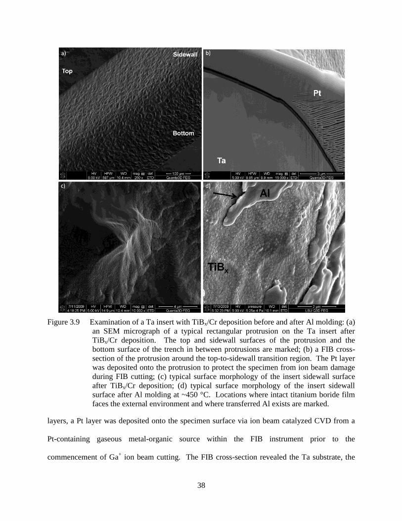
Figure 3.9(a) shows an SEM micrograph of one rectangular microprotrusion on another
Ta insert, onto which TiBx/Cr layers were deposited. Figure 3.9(b) shows a FIB cross-section
around the region of the protrusion top surface to sidewall transition. To protect the TiBx/Cr
38
Figure 3.9 Examination of a Ta insert with TiBx/Cr deposition before and after Al molding: (a)
an SEM micrograph of a typical rectangular protrusion on the Ta insert after
TiBx/Cr deposition. The top and sidewall surfaces of the protrusion and the
bottom surface of the trench in between protrusions are marked; (b) a FIB cross-
section of the protrusion around the top-to-sidewall transition region. The Pt layer
was deposited onto the protrusion to protect the specimen from ion beam damage
during FIB cutting; (c) typical surface morphology of the insert sidewall surface
after TiBx/Cr deposition; (d) typical surface morphology of the insert sidewall
surface after Al molding at ~450 °C. Locations where intact titanium boride film
faces the external environment and where transferred Al exists are marked.
layers, a Pt layer was deposited onto the specimen surface via ion beam catalyzed CVD from a
Pt-containing gaseous metal-organic source within the FIB instrument prior to the
commencement of Ga+ ion beam cutting. The FIB cross-section revealed the Ta substrate, the

39
elemental Cr interlayer with the lighter contrast, and the TiBx top layer with the darker contrast.
Figure 3.9(b) demonstrates the conformal nature of the deposited TiBx/Cr layers. Additional
examinations clearly showed that the TiBx/Cr conformal coverage extended to the entire Ta
insert, including the protrusion top surfaces, all the sidewall surfaces, and the bottom surfaces.
Figure 3.9(c) shows the typical morphology of the protrusion sidewall surface after TiBx/Cr
deposition. The TiBx top layer covered the entire sidewall surface, including all the microscale
undulations resulting from the EDM/ECP processes. Figure 3.9(d) shows a magnified view of
the insert sidewall surface, after three Al molding runs were executed at ~450 °C. Figure 3.9(d)
clearly shows that Al was transferred to the insert during the molding/demolding processes and
that the TiBx top layer remained intact without delamination after Al molding, despite the Al
transfer.
Past observations of TiB2 coatings in sliding contact against Al in a rotating cylinder
configuration have identified coating detachment from the TiB2/substrate interface as an
additional degradation mechanism [29]. Whether coating detachment from the Ta insert would
occur in the present micromolding configuration cannot be deduced from previous macroscale
observations. Results shown in Figure 3.9 suggest that conformal TiBx/Cr coatings deposited
onto Ta mold inserts by ICP assisted balanced magnetron sputtering possess sufficient adhesion
such that contact induced coating delamination does not occur during Al micromolding. Figure
3.9(d) also suggests that intimate contact between the transferred Al material and the insert with
conformally deposited TiBx/Cr layers does not seem to occur uniformly. Al chips transferred
onto the insert sidewall surfaces showed “flare up” around the edges, suggesting that adhesion
between Al and the TiBx film is not strong. Such evidence is consistent with previous
observations of macroscale Al transfer onto TiB2 coated disks during pin-on-disk type sliding

40
contact: Al transferred onto the TiB2 surface during initial sliding was liberated and turned into
loose debris during further sliding; the amount of Al transferred further depended on the
roughness of the TiB2 surface, with increased Al transfer onto rougher surfaces [16]. Present
observations on Al transfer onto sidewall surfaces of Ta inserts with conformally deposited
TiBx/Cr layers also suggest that the micron scale surface undulations present on the Ta inserts
due to the EDM/ECP processes contribute to Al transfer. Further studies regarding the
application of titanium boride thin films to insert surface engineering for Al micromolding
applications remain to be conducted, especially on the influence of insert surface roughness and
insert geometry on molding performance.
Deposition of TiBx/Cr thin films onto planar Si(100) and non-planar Ta substrates was
carried out by balanced magnetron sputtering and ICP assisted balanced magnetron sputtering.
Characterization of TiBx thin films suggested that increase in film densification occurred with
increasing ion bombardment due to the ICP assist, despite the low-temperature deposition. The
morphology of TiBx thin films deposited onto microscale non-flat Ta substrates was examined.
The effectiveness of conformal TiBx thin films as reaction barriers for microscale compression
molding of Al was studied by carrying out Al molding experiments at ~450 °C. The present
results show that the TiBx/Cr thin films can withstand repeated contact with Al at elevated
temperatures in molding applications without delamination.
3.4 References
[1] Madou M, Fundamentals of Microfabrication. CRC Press, Boca Raton (1997).
[2] Cao DM, Wang T, Feng B, Meng WJ, Kelly KW, Amorphous hydrocarbon based thin
films for high-aspect-ratio MEMS applications. Thin Solid Films 398/399:553 (2001).
[3] Cao DM, Meng WJ, Simko SJ, Doll GL, Wang T, Kelly KW, Conformal deposition of
Ti-containing hydrocarbon coatings over LiGA fabricated high-aspect-ratio micro-scale
structures and tribological characteristics. Thin Solid Films 429:46 (2003).
41
[4] Cao DM, Meng W, Microscale compression molding of Al with surface engineered
LiGA inserts. Microsyst. Technol. 10:662 (2004).
[5] Cao DM, Jiang J, Meng WJ, Jiang JC, Wang W, Fabrication of high-aspect-ratio
microscale Ta mold inserts with micro-electrical-discharge-machining. Microsyst.
Technol. 13:503 (2007).
[6] Jiang J, Mei Fanghua, Meng WJ, Lara-Curzio E, Microscale molding replication of Cu-
and Ni- based structures. Microsyst. Technol. 14:1731 (2008).
[7] Jiang J, Mei Fanghua, Meng WJ, Fabrication of metal-based high-aspect-ratio microscale
structures by compression molding. J. Vac. Sci. Technol. A26:745 (2008).
[8] Mei Fanghua, Parida PR, Jiang J, Meng WJ, Ekkad SV, Fabrication, assembly, and
testing of Cu- and Al- based microchannel heat exchangers. JMEMS 17:869 (2008).
[9] Zhang L, Chen Min, Li Zheyi, Chen Dihu, Pan Shirong, Effect of annealing on structure
and haemocompatibility of tetrahedral amorphous hydrogenated carbon films. Mater.
Lett. 62:1040 (2008).
[10] Lin Yu-Hung, Lin Hong-Da, Liu Chun-Kuo, Huang Meng-Wen, Chen Ya-Chi, Chen
Jiann-Ruey, Shih Han C., Annealing effect on the structural, mechanical and electrical
properties of titanium-doped diamond-like carbon films. Thin Solid Films 518:1503
(2009).
[11] Pierson HO, Mullendore AW, The chemical vapor-deposition of TiB2 from diborane.
Thin Solid Films 72:511 (1980).
[12] Pierson HO, Mullendore AW, Thick boride coatings by chemical vapor-deposition. Thin
Solid Films 95:99 (1982).
[13] Williams LM, Plasma enhanced chemical vapor deposition of titanium diboride films.
Appl. Phys. Lett. 46:43 (1985).
[14] Lee SH, Nam KH, Hong SC, Lee JJ, Low temperature deposition of TiB2 by inductively
coupled plasma assisted CVD. Surf. Coat. Technol. 201:5211 (2007).
[15] Mayrhofer PH, Mitterer C, Wen JG, Greene JE, Petrov I, Self-organized nanocolumnar
structure in superhard TiB2 thin films. Appl. Phys. Lett. 86:131909 (2005).
[16] Konca E, Cheng YT, Weiner AM, Dasch JM, Erdemir A, Alpas AT, Transfer of 319 Al
alloy to titanium diboride and titanium nitride based (TiAlN, TiCN, TiN) coatings:
effects of sliding speed, temperature and environment. Surf. Coat. Technol. 200:2260
(2005).
[17] Chattopadhyay AK, Roy P, Sarangi SK, Study of wettability test of pure aluminum
against uncoated and coated carbide inserts. Surf. Coat. Technol. 204:410 (2009).
42
[18] Meng WJ, Curtis TJ, Inductively coupled plasma assisted physical vapor deposition of
titanium nitride coatings. J. Electron. Mater. 26:1297 (1997).
[19] Meng WJ, Meletis EI, Rehn LE, Baldo PM, Inductively-coupled plasma assisted
deposition and mechanical properties of metal-free and Ti-containing hydrocarbon
coatings. J. Appl. Phys. 87:2840 (2000).
[20] Shi B, Meng WJ, Intrinsic stresses and mechanical properties of Ti-containing
hydrocarbon coatings. J. Appl. Phys. 94:186 (2003).
[21] Lieberman MA, Lichtenberg AJ, Principles of Plasma Discharges and Materials
Processing, 2nd edition. Wiley, Hoboken, New Jersey (2005).
[22] Shi B, Meng WJ, Rehn LE, Baldo PM, Intrinsic stress development in Ti-C:H ceramic
nanocomposite coatings. Appl. Phys. Lett. 81:352 (2002).
[23] Mavel G, Escard J, Costa P, Castaing J, ESCA surface study of metal borides. Surf. Sci.
35:109 (1973).
[24] Wagner CD, Riggs WM, Davis LE, Moulder JF, Muilenberg GE (editors), Handbook of
X-ray Photoelectron Spectroscopy. Perkin-Elmer Physical Electronics, Eden Prairie,
Minnesota (1979).
[25] Munro RG, Material Properties of Titanium Diboride. J. Res. Natl. Inst. Stand. Technol.
105:709 (2000).
[26] Berger M, Larsson M, Hogmark S, Evaluation of magnetron-sputtered TiB2 intended for
tribological applications. Surf. Coat. Technol. 124:253 (2000).
[27] Meng WJ, Curtis TJ, Rehn LE, Baldo PM, Temperature dependence of inductively
coupled plasma assisted deposition of titanium nitride coatings. Surf. Coat. Technol.
120/121:206 (1999).
[28] Jiang J, Sinclair GB, Meng WJ, Quasi-static normal indentation of an elasto-plastic
substrate by a periodic array of elastic strip punches. Int. J. Solids Struct. 46:3677 (2009).
[29] Berger M, Hogmark S, Evaluation of TiB2 coatings in sliding contact against aluminum.
Surf. Coat., Technol. 149:14 (2002).
43
CHAPTER 4
TWO METHOD OF MEASURING INTERFACIAL SHEAR STRESS
4.1 Introduction
Agrawal and Raj performed uniaxial tensile testing of ductile metallic substrates on top
of which brittle thin ceramic coatings are deposited. They pointed out that an evaluation of the
limiting shear strength of the coating/substrate interfacial region can be achieved by examining
cracks formed in the ceramic coating due to tensile deformation of the ductile substrate [1]. The
same strain is experienced by the thin coating as the substrate is deformed, with the substrate
strain being predominantly plastic and the coating strain being elastic. This strain leads to
transverse cracking in the coating perpendicular to the direction of tensile loading. The density
of such transverse cracks increases with increasing substrate plastic strain to a plateau value,
beyond which further increase in substrate plastic strain does not cause additional decrease in
crack spacing. An apparent failure stress in tension is derived for the coating [1],
fE ˆ , (4.1)
where E and f are respectively the Young’s modulus of the coating and the strain at which
transverse cracks in the coating develops. Combining this apparent failure stress with the
saturation spacing of transverse cracks in the coating at large substrate strain, a limiting shear
strength of the coating/substrate interfacial region is derived [1],
ˆ
ˆˆ , (4.2)
where is the coating thickness and ̂ is the saturation spacing between transverse cracks.
Thus, a quantitative evaluation of this limiting interfacial shear strength can be achieved through
measurement of the density of transverse cracks in the coating as a function of substrate tensile
loading.
44
In this paper, two experimental attempts of assessing the limiting shear strength of
coating/substrate interfacial regions have been described. The assessment through examination
of transverse coating cracks induced by tensile substrate loading has been exemplified through
experiments on TiN/Cr/steel and TiN/Ti/steel specimens. Failure of coating/substrate interfacial
region induced by compression loading of micro pillars containing inclined interfaces has been
illustrated through preliminary experiments conducted on TiN/Ti/Si specimens. This
methodology is new and can yield a direct measure of the critical failure stress.
4.2 Experimental Procedures
An inductively coupled plasma (ICP) assisted chemical/physical vapor deposition
(CVD/PVD) tool was used to deposit TiN coatings onto SAE1018 steel with three elemental Ti
(99.95%) targets and one Cr (99.95%) in an Ar/N2 mixture. Steel substrates were machined into
shapes of rectangular tensile bars. The tensile bars have gauge section cross-sectional
dimensions of 6mm×4mm and a gauge length of 25mm [2]. They were mechanically polished to
a smooth surface, cleaned in acetone and methanol, dried, and loaded into the deposition system.
The substrates were rotated at ~12rpm during deposition. Deposition started with a plasma
surface etch in a 13.56MHz Ar (99.999%) ICP with a total pressure of ~10mTorr. The total
input power into the rf ICP was 1000W, and the substrate bias was -50V. Immediately following
the substrate surface etch, an elemental Ti or Cr intermediate adhesion layer was deposited onto
the steel substrate via balanced magnetron sputtering in Ar. After the Ti or Cr interlayer
deposition, a TiN coating layer was deposited with ICP assist at a total input rf power of 1000W
in an Ar/N2 mixture. The Ar/N2 gas input flow ratio was kept at slightly below the pressure
hysteresis point, which signifies a change of Ti target surface condition from metallic to fully
nitrided [ 3 ]. In so doing, nearly stoichiometric TiN deposition was achieved without a
45
significant decrease in the deposition rate. The total pressure during TiN deposition was below
11mTorr. No intentional substrate heating was applied. The substrate bias was kept at -50V
throughout the Ti or Cr interlayer and the TiN top layer deposition. The third series of TiN
coatings were deposited on 2 inch diameter, methanol, acetone cleaned silicon wafers.
Immediately after same etching process, an elemental Ti interlayer, ~200nm in thickness, was
deposited onto the substrate by sputtering the Ti targets in Ar with ICP assist. Deposition of TiN
coating layers, ~5μm in thickness, occurred immediately after Ti interlayer deposition. An
electrical bias voltage of -30V was applied to the substrate during TiN deposition.
As deposited TiN/Ti/Si(100) films were cut into small pieces and bonded with two
similar size stainless steel sheet metal, then milled into micro pillars for displacement control
compression test by NaNoindenter XP system[4].
Scanning electron microscopy was conducted on a Hitachi S3600N microscope and an
FEI Quanta3D FEG system in a field emission electron beam/focused Ga+ ion beam (FIB) dual-
beam configuration, with X-ray energy dispersive spectroscopy (EDS) capabilities. Both
electron-induced secondary electron (SE) and ion-induced secondary electron (ISE) images can
be acquired. Transmission electron microscopy (TEM) was carried out on a JEOL JEM2010
microscope operated at 200kV, again with EDS capabilities. X-ray diffraction (XRD)
experiments were carried out on a PANalytical Empyrean system with a graphite mirror
incidence beam monochromator, a 5-axes cradle sample stage, and a PIXcel3D photon counting
detector.
Uniaxial tensile testing of bar specimens was carried out at room temperature on an MTS
858 system equipped with hydraulic grippes. Loading forces were measured with a MTS
46
661.19F-04 load cell. Strains in bar gauge sections were measured with an MTS 632.26F-20
extensometer.
4.3 Results and Discussion
Figure 4.1 shows a Ga+ FIB cross section into the surface of one typical TiN/Ti/steel
specimen in the as-deposited state. Prior to FIB cutting, a Pt layer was deposited onto the
specimen surface via Ga+ catalyzed deposition from a Pt-containing gaseous organometallic
source to protect the coating surface. In the cross section, the steel substrate, the Ti interlayer,
and the TiN top layer are clearly visible. The columnar structure of the TiN layer is also evident.
Measurements of the thickness of the Ti or Cr interlayer and the TiN top layer were obtained
from FIB cross sections such as that shown in Figure 4.1.
Figure 4.1 An SE image of a FIB cross-section of a typical TiN/Ti/steel specimen. The two
small arrows denote the TiN/Ti and Ti/steel interfaces.
Two series of TiN coatings were deposited onto steel tensile bar specimens, both in the
configuration of TiN/interlayer/steel. For the first specimen series, an elemental Cr interlayer
was deposited onto steel, followed by the TiN top layer. The thicknesses of the interlayer and
47
the top layer were ~270nm and ~1.5μm, respectively, and kept nominally the same for all
specimens in the series. For the second specimen series, an elemental Ti interlayer was
deposited onto steel, followed by the TiN top layer. The thicknesses of the interlayer and the top
layer were ~300nm and ~2.7μm, respectively, and kept nominally the same for all specimens in
the series.
Figure 4.2(a) shows a plan-view SE image of one TiN/Cr/steel specimen, loaded in
uniaxial tension to a total strain of 2.79%. The formation of long and straight cracks
Figure 4.2 (a) A plan-view SE image of one TiN/Cr/steel specimen pulled to a total tensile
strain of 2.79%; (b) a plan-view SE image of one TiN/Ti/steel specimen pulled to
a total tensile strain of 4.06%. One ~45 crack is highlighted in the circle. Arrows
denote the tensile direction.
perpendicular to the tensile direction is evident in Figure 4.2(a). Figure 4.2(b) shows a plan-view
SE image of one TiN/Ti/steel specimen, loaded to a total tensile strain of 4.06%. In addition to
the long transverse cracks, secondary cracks oriented ~45 to the tensile direction are evident in
Figure 4.2(b). These ~45 oriented cracks develop as the total tensile strain increases to 3% and
above, and have been observed in previous in-situ observations by Chen et al. of transverse crack
development in tensile loaded TiN/steel specimens [5]. These ~45 cracks are believed to be due
48
to substrate contraction perpendicular to the tensile direction after the transverse cracks have
already formed, and are therefore not relevant to the determination of interfacial shear strength.
Figure 4.3 shows an SE image of a FIB cross section across a typical transverse crack in
one TiN/Ti/steel specimen, loaded to a total tensile strain of 2.47%. The steel substrate, the Ti
Figure 4.3 A cross sectional SE image of one TiN/Ti/steel specimen across a transverse
crack. The large arrows denote the tensile direction, and the small arrows denote
the TiN/Ti and Ti/steel interfaces.
interlayer, and the TiN coating layer are clearly visible in the cross section. Figure 4.3 indicates
that the transverse crack goes through the entire TiN layer as well as the Ti interlayer, and stops
at the Ti/steel interface. The mark on the cross sectional surface of the steel substrate, continuing
from the transverse crack, is an artifact of the Ga+ irradiation from the top direction in the
presence of the crack. In particular, Figure 4.3 shows that the transverse crack did not turn and
extend into the TiN/Ti or Ti/steel interface.
From images such as those shown in Figure 4.2, the density of transverse cracks is
assessed by counting the length of transverse cracks in an image area of ~190μm×160μm.
Consistent with the previous discussion, only the transverse cracks were counted and the ~45
oriented cracks were not taken into account. For each value of total tensile strain, 3 to 7 separate
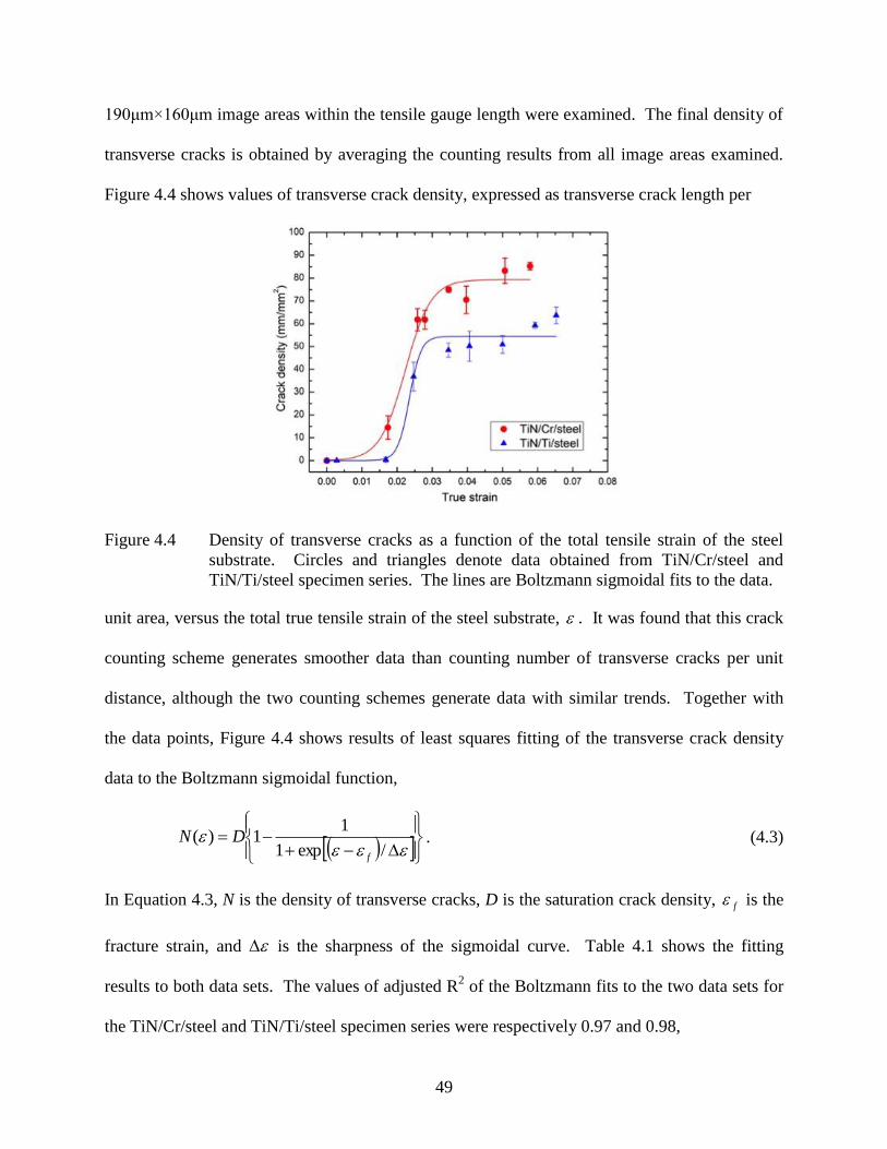
49
190μm×160μm image areas within the tensile gauge length were examined. The final density of
transverse cracks is obtained by averaging the counting results from all image areas examined.
Figure 4.4 shows values of transverse crack density, expressed as transverse crack length per
Figure 4.4 Density of transverse cracks as a function of the total tensile strain of the steel
substrate. Circles and triangles denote data obtained from TiN/Cr/steel and
TiN/Ti/steel specimen series. The lines are Boltzmann sigmoidal fits to the data.
unit area, versus the total true tensile strain of the steel substrate, . It was found that this crack
counting scheme generates smoother data than counting number of transverse cracks per unit
distance, although the two counting schemes generate data with similar trends. Together with
the data points, Figure 4.4 shows results of least squares fitting of the transverse crack density
data to the Boltzmann sigmoidal function,
/exp1
11)(
f
DN . (4.3)
In Equation 4.3, N is the density of transverse cracks, D is the saturation crack density, f is the
fracture strain, and is the sharpness of the sigmoidal curve. Table 4.1 shows the fitting
results to both data sets. The values of adjusted R2 of the Boltzmann fits to the two data sets for
the TiN/Cr/steel and TiN/Ti/steel specimen series were respectively 0.97 and 0.98,
50
Table 4.1 Results of Boltzmann sigmoidal curve fit to experimentally measured transverse
crack density in TiN coatings deposited onto steel substrates
Specimen
series
f (%)
(%)
D
(mm/mm2)
Adj. R2 ̂ (μm) (μm)
TiN/Cr/steel 2.2±0.1 0.4±0.1 79±3 0.97 12.7±0.5 1.5
TiN/Ti/steel 2.4±0.2 0.2±0.2 55±2 0.96 18.2±0.7 2.7
demonstrating similar and reasonable fit qualities. From the Boltzmann fits to the data obtained
from the TiN/Cr/steel and TiN/Ti/steel specimen series, the values of f were determined to be
2.2±0.1% and 2.4±0.2%, respectively. The values of , which governs the sharpness of the
sigmoidal curves, were similar, with associated with the data for the TiN/Cr/steel specimen
series being slightly larger. Reasonable agreement exists between the two f values obtained
from two independently deposited series of TiN coatings. The mean value of presently
determined f , 2.3±0.2%, is in general agreement with in-situ observations of Chen et al.: they
obtained f = 2.56% from tensile loaded TiN/steel specimens made by hollow cathode discharge
ion plating [5]. The apparent failure stress in tension for the present two series of TiN coatings is
fE = 9.8±0.9GPa, taking f = 2.3±0.2% and E = 427GPa [6]. The saturation spacing between
transverse cracks, ̂ , is the inverse of D. The values of ̂ for the TiN/Cr/steel and TiN/Ti/steel
specimen series are also shown in Table 4.1. It should be noted that ceramic coatings deposited
with ion or plasma assist can contain significant level of intrinsic stresses [7], with the total
residual stress within the coating often dominated by intrinsic stresses [8]. In the presence of a
residual stress R , Equation 4.1 is modified to [5]
RfE ˆ . (4.4)
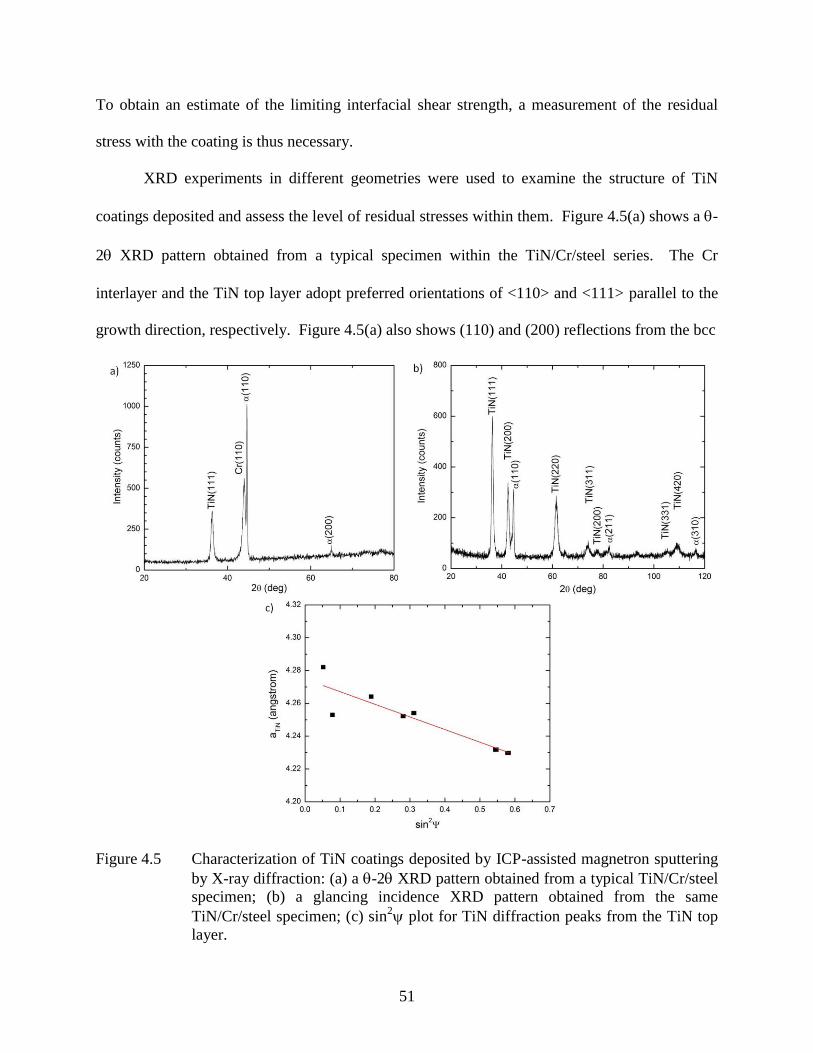
51
To obtain an estimate of the limiting interfacial shear strength, a measurement of the residual
stress with the coating is thus necessary.
XRD experiments in different geometries were used to examine the structure of TiN
coatings deposited and assess the level of residual stresses within them. Figure 4.5(a) shows a -
2 XRD pattern obtained from a typical specimen within the TiN/Cr/steel series. The Cr
interlayer and the TiN top layer adopt preferred orientations of <110> and <111> parallel to the
growth direction, respectively. Figure 4.5(a) also shows (110) and (200) reflections from the bcc
Figure 4.5 Characterization of TiN coatings deposited by ICP-assisted magnetron sputtering
by X-ray diffraction: (a) a -2 XRD pattern obtained from a typical TiN/Cr/steel
specimen; (b) a glancing incidence XRD pattern obtained from the same
TiN/Cr/steel specimen; (c) sin2 plot for TiN diffraction peaks from the TiN top
layer.
52
α-phase of the steel substrate. Figure 4.5(b) shows a glancing incidence XRD pattern obtained
from the same specimen. In the glancing incidence diffraction geometry, the X-ray incidence
angle was fixed at = 5 and the detector angle was scanned to obtain diffraction signals in the
range of 20 < 2 < 120. The angle, the angle between the scattering vector k
and the
sample surface normal n
, is given by [9]. A multitude of B1 TiN reflections are
evident in Figure 4.5(b), together with several reflections from the α-phase of steel. The Cr(110)
reflection is overwhelmed by the α(110) reflection. Figure 4.5(c) shows a 2sin plot for the
TiN top layer in the TiN/Cr/steel specimen. In Figure 4.5(c), values of B1 lattice constant aTiN
calculated from all TiN reflections shown in Figure 4.5(b) is plotted vs. 2sin . A reasonable
linear correlation is evident. Assuming an equal biaxial stress R within the TiN layer, the
2sin plot is used to derive the residual stress within the coating [10]:
oRoR aE
aE
a
21sin
1 2. (4.5)
A linear least squares fit to the data shown in Figure 4.5(c) yields a slope of -0.0077±0.0011nm
and an intercept of 0.4275±0.0011nm, with an adjusted R2 of 0.78. The value of ao was taken to
be 0.424nm, the bulk lattice parameter of B1 TiN [ 11 ]. Values of E and were taken
respectively to be 427GPa and 0.194, corresponding to the Hashin and Shtrikman average for
random polycrystalline aggregates of TiN [6,12]. From the fitted slope of the 2sin plot,
Equation 4.5 yields R = -6.5±0.9GPa, i.e., a compressive residual stress. The value of the
2sin intercept is then calculated to be 0.4265nm, consistent with the fitted intercept value of
0.4275nm. Taking fE = 9.8±0.9GPa and R = -6.5±0.9GPa, values of the limiting interfacial
shear strength for the TiN/Cr/steel and TiN/Ti/steel specimen series are calculated from Equation
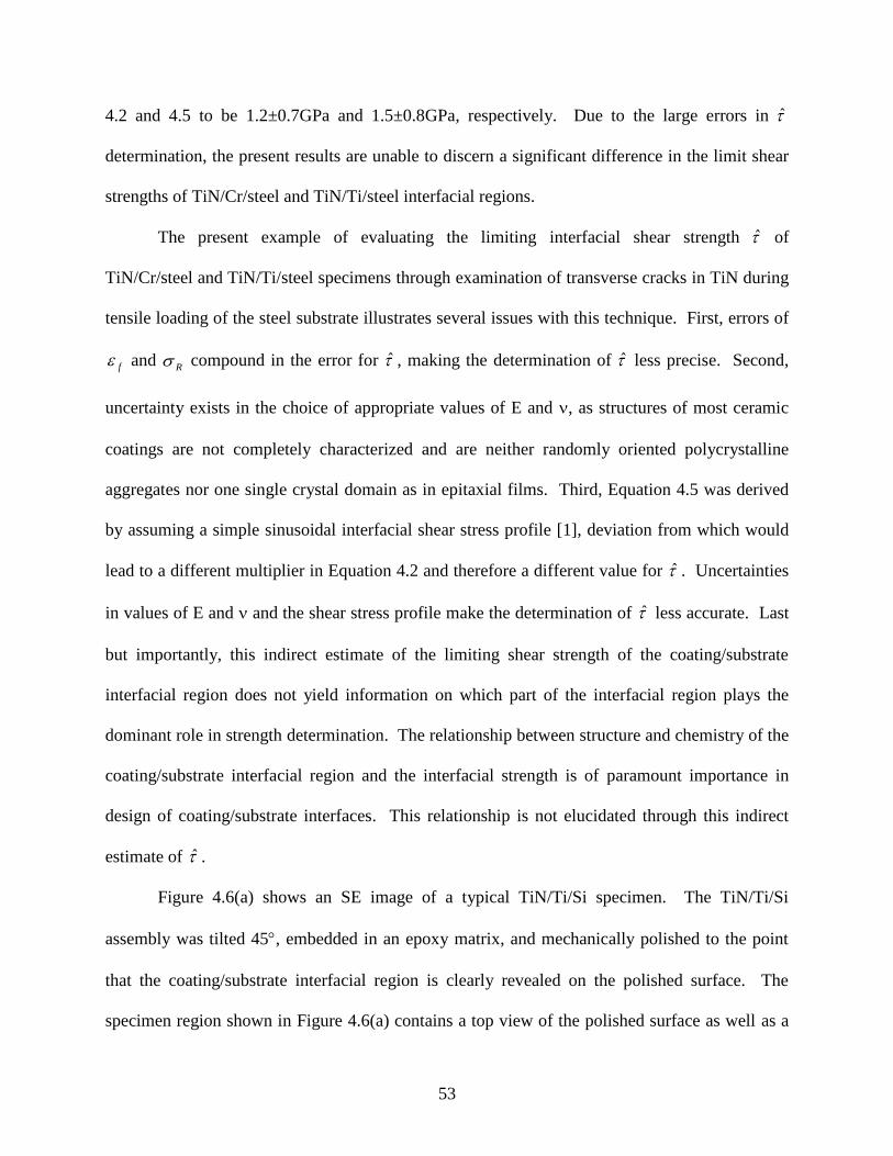
53
4.2 and 4.5 to be 1.2±0.7GPa and 1.5±0.8GPa, respectively. Due to the large errors in ̂
determination, the present results are unable to discern a significant difference in the limit shear
strengths of TiN/Cr/steel and TiN/Ti/steel interfacial regions.
The present example of evaluating the limiting interfacial shear strength ̂ of
TiN/Cr/steel and TiN/Ti/steel specimens through examination of transverse cracks in TiN during
tensile loading of the steel substrate illustrates several issues with this technique. First, errors of
f and R compound in the error for ̂ , making the determination of ̂ less precise. Second,
uncertainty exists in the choice of appropriate values of E and , as structures of most ceramic
coatings are not completely characterized and are neither randomly oriented polycrystalline
aggregates nor one single crystal domain as in epitaxial films. Third, Equation 4.5 was derived
by assuming a simple sinusoidal interfacial shear stress profile [1], deviation from which would
lead to a different multiplier in Equation 4.2 and therefore a different value for ̂ . Uncertainties
in values of E and and the shear stress profile make the determination of ̂ less accurate. Last
but importantly, this indirect estimate of the limiting shear strength of the coating/substrate
interfacial region does not yield information on which part of the interfacial region plays the
dominant role in strength determination. The relationship between structure and chemistry of the
coating/substrate interfacial region and the interfacial strength is of paramount importance in
design of coating/substrate interfaces. This relationship is not elucidated through this indirect
estimate of ̂ .
Figure 4.6(a) shows an SE image of a typical TiN/Ti/Si specimen. The TiN/Ti/Si
assembly was tilted 45, embedded in an epoxy matrix, and mechanically polished to the point
that the coating/substrate interfacial region is clearly revealed on the polished surface. The
specimen region shown in Figure 4.6(a) contains a top view of the polished surface as well as a
54
FIB-cut cross sectional view into the polished surface. The FIB cross section reveals the inclined
TiN/Ti/Si interface region. The elemental Ti interlayer in between the Si substrate and the TiN
coating is visible though its lighter contrast. Figure 4.6(b) shows a typical microscale cylindrical
pillar defined by Ga+ FIB milling conducted perpendicular to the polished surface. The micro
pillar contains the TiN/Ti/Si interface region at a 45 inclination with respect to the pillar axis.
Figure 4.6 Micro pillar fabrication by FIB milling: (a) an SE image of the FIB cross section
of a TiN/Ti/Si specimen, tilted 45 and polished to reveal the interface region; (b)
an SE image of a typical micropillar FIB cut from the 45 tilted TiN/Ti/Si
specimen.
Figure 4.7 shows a typical measured raw load - displacement curve. For each pillar, the
load increased approximately linearly with increasing indenter displacement at the beginning.
Then the pillar failed abruptly when the load reached a breaking point, manifested in a large and
abrupt displacement excursion: typically 4-5µm for a pillar diameter ~3 µm.
Figure 4.8 illustrate typical measurement scatter from multiple micro pillars, and indicate,
within the experimental scatter, that there is not a significant dependence of the average
interfacial shear stress at failure on the pillar diameter over the range of pillars tested. While

55
additional studies are needed to ascertain the exact nature of the compression induced interfacial
failure, the average value of all data points shown in Figure 4.8, 1.0±0.1GPa, is curiously close
Figure 4.7 Compression testing of micro pillars containing inclined TiN/Ti/Si interfaces: a
typical load-displacement curve obtained during compression testing of one 3μm
diameter TiN/Ti/Si micro pillar containing a 45 inclined TiN/Ti/Si interface.
to the limiting interfacial shear strength determined through examination of transverse cracks
induced by tensile loading in the TiN/Cr/steel and TiN/Ti/steel specimen series. The
methodology of directly inducing interfacial failures by compression loading of micro pillars
Figure 4.8 Values of the average shear stress at failure by compression loading of TiN/Ti/Si
micro pillars containing 45 inclined interfaces as a function of the pillar diameter.
56
containing inclined coating/substrate interfaces is new, can potentially yield an accurate measure
of the critical failure stress, and deserves to be further explored.
4.4 References
[1] D.C. Agrawal, R. Raj, Measurement of the ultimate shear strength of a metal-ceramic
interface, Acta Metall. 37, 1265 (1989).
[2] ASTM Standard E 8/E 8M – 08, Standard test methods for tension testing of metallic
materials, ASTM International, West Conshohocken, Pennsylvania, U.S.A.
[3] W.D. Westwood, in Physics of Thin Films, edited by M.H. Francombe and J.L. Vossen
(Academic Press, Boston, 1989), Vol. 14, p. 1.
[4] Ke Chen, Yang Mu, Wen Jin Meng, A new experimental approach for evaluating the
mechanical integrity of interfaces between hard coatings and substrates, MRS Comm. 4,
19-23 (2014).
[5] B.F. Chen, J. Hwang, G.P. Yu, J.H. Huang, In situ observation of the cracking behavior
of TiN coatings on 304 stainless steel subjected to tensile strain, Thin Solid Films 352,
173 (1999).
[6] W.J. Meng, G.L. Eesley, Growth and mechanical anisotropy of TiN thin films, Thin Solid
Films 271, 108 (1995).
[7] J.E. Greene, S.A. Barnett, J.E. Sundgren, A. Rockett, Low energy ion/surface interactions
during film growth from the vapor phase, in Ion Beam Assisted Film Growth, edited by T.
Itoh, Elsevier, Amsterdam (1989).
[8] W.J. Meng, J.A. Sell, T.A. Perry, L.E. Rehn, P.M. Baldo, Growth of aluminum nitride
thin films on Si(111) and Si(100): structural characteristics and development of intrinsic
stresses, J. Appl. Phys. 75, 3446 (1994).
[9] A.J. Perry, J.A. Sue, P.J. Martin, Practical measurement of the residual stress in coatings,
Surf. Coat. Technol. 81, 17 (1996).
[10]. B.D. Cullity, S.R. Stock, Elements of X-ray Diffraction, 3rd
edition, Prentice Hall, New
Jersey (2001).
[11] L.E. Toth, Transition Metal Carbides and Nitrides, Academic Press, New York (1971).
[12] Z. Hashin, S. Shtrikman, A variational approach to the theory of the elastic behaviour of
polycrystals, J. Mech. Phys. Solids 10, 343 (1962).

57
CHAPTER 5
THICKNESS DEPENDENCE OF FLOW STRESS OF CU THIN FILMS IN
CONSTRAINED SHEAR PLASTIC FLOW
5.1 Introduction
Size effects in plasticity have been documented through many experiments over the past
two decades, including torsion of wires [1], indentation by pyramidal indenters [2], and bending
of beams [3]. Shearing of a well-bonded metal layer sandwiched between two substrates which
do not deform plastically has been one of the canonical cases studied in the development of
strain gradient plasticity. In many respects, it captures in the simplest manner the essence of
plastic strain gradients associated with geometrically necessary dislocations generated when
plastic flow is blocked at the metal/substrate interfaces. Analytically, shear of confined layers is
one of the simplest problems to solve, as illustrated in the following selection of theoretical
papers on the subject [ 4 , 5 , 6 , 7 , 8 ]. Experimentation was performed previously in the
configuration of shear loading of thin Al layers diffusion bonded between Al2O3 adherents [9].
The results of this experimentation, however, were inconclusive. Until now, experimental data
for the confined shear problem have not been available to confront the theoretical predictions.
Shear plastic flow in confined thin layers, in addition to its scientific interest in furthering
exploration of plasticity size effects, is of significant technological interest. Over the past two
decades, vapor phase deposition of thin ceramic coatings has become an important means for
engineering surfaces of mechanical components [10] and manufacturing tools [11]. Satisfactory
adhesion of coatings to substrates is critical to the lifetime of coated systems and often the
deciding factor for their implementation. To improve adhesion, interfacial adhesion layers are
deposited between the ceramic coating and the substrate. Such interlayers often consist of
elemental metals. When coated components are subjected to external load, shear strength of the
interface region can become the limiting factor on how mechanical load is transmitted from the
58
substrate to the top coating [12]. Quantitative measurements of shear plastic flow in confined
thin layers and correlation of such flow stress to their structure and composition are therefore
important for engineering improved coating/adhesion-layer/substrate systems.
The dominant experimental means for determining yield strength of thin metal films at
present is instrumented nanoindentation. However, mechanical property evaluation by indenting
films on substrates encounters difficulties at small film thicknesses due to substrate influence
[13]. A new experimental protocol for evaluating the mechanical integrity of interfaces between
hard coatings and substrates was demonstrated recently [14]. Vapor phase deposited specimens
in the configuration of coating/interlayer/substrate were fabricated via focused ion beam (FIB)
into microscale cylindrical pillars. To make micro-pillars without significant taper, a FIB script
program was employed [ 15 ] which enabled a lathe-like milling process with Ga+ ions.
Specimens were oriented such that the coating/interlayer/substrate interface is inclined with
respect to the pillar axis. Interfacial failures were then achieved through compression loading of
the pillars in the axial direction [14]. When the coating and the substrate are both elastic-brittle
materials, compression loading of pillars with inclined interfaces results in a predominantly shear
loading on the interlayer. This test configuration therefore presents a suitable geometry for
experimental evaluation of shear plastic flow of confined layers. We report here results of
compression testing on CrN/Cu/Si(100) micro-pillars containing 45-inclined interfaces.
5.2 Experimental Procedures
Deposition of CrN coatings was carried out in an ultra-high-vacuum vapor deposition
tool, which housed a 13.56MHz inductively coupled plasma (ICP) and four balanced magnetron
sputter guns [16]. All guns faced the center of the deposition chamber, with a base pressure of <
5×10⁻⁹
Torr. Cleaned Si(100) substrates, 50.8mm in diameter, were placed into a load lock,
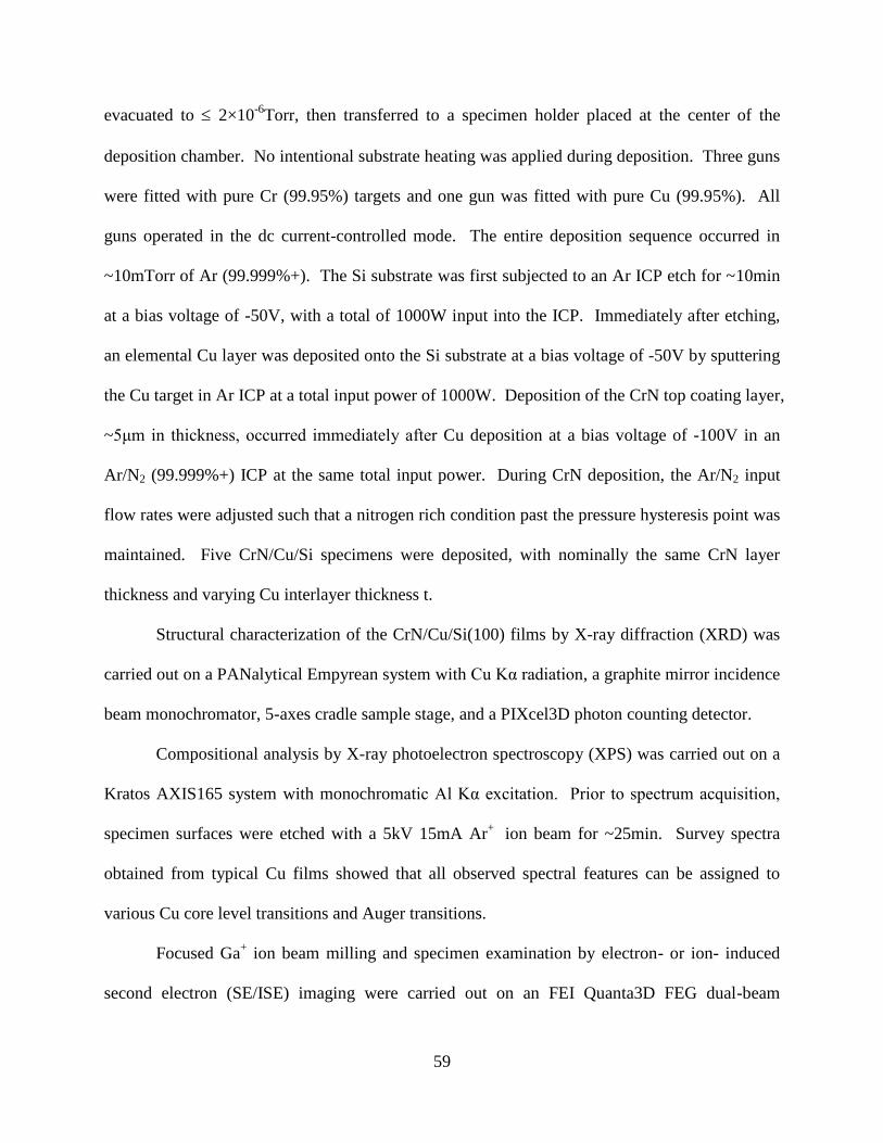
59
evacuated to 2×10⁻⁶
Torr, then transferred to a specimen holder placed at the center of the
deposition chamber. No intentional substrate heating was applied during deposition. Three guns
were fitted with pure Cr (99.95%) targets and one gun was fitted with pure Cu (99.95%). All
guns operated in the dc current-controlled mode. The entire deposition sequence occurred in
~10mTorr of Ar (99.999%+). The Si substrate was first subjected to an Ar ICP etch for ~10min
at a bias voltage of -50V, with a total of 1000W input into the ICP. Immediately after etching,
an elemental Cu layer was deposited onto the Si substrate at a bias voltage of -50V by sputtering
the Cu target in Ar ICP at a total input power of 1000W. Deposition of the CrN top coating layer,
~5μm in thickness, occurred immediately after Cu deposition at a bias voltage of -100V in an
Ar/N2 (99.999%+) ICP at the same total input power. During CrN deposition, the Ar/N2 input
flow rates were adjusted such that a nitrogen rich condition past the pressure hysteresis point was
maintained. Five CrN/Cu/Si specimens were deposited, with nominally the same CrN layer
thickness and varying Cu interlayer thickness t.
Structural characterization of the CrN/Cu/Si(100) films by X-ray diffraction (XRD) was
carried out on a PANalytical Empyrean system with Cu Kα radiation, a graphite mirror incidence
beam monochromator, 5-axes cradle sample stage, and a PIXcel3D photon counting detector.
Compositional analysis by X-ray photoelectron spectroscopy (XPS) was carried out on a
Kratos AXIS165 system with monochromatic Al Kα excitation. Prior to spectrum acquisition,
specimen surfaces were etched with a 5kV 15mA Ar+
ion beam for ~25min. Survey spectra
obtained from typical Cu films showed that all observed spectral features can be assigned to
various Cu core level transitions and Auger transitions.
Focused Ga+ ion beam milling and specimen examination by electron- or ion- induced
second electron (SE/ISE) imaging were carried out on an FEI Quanta3D FEG dual-beam
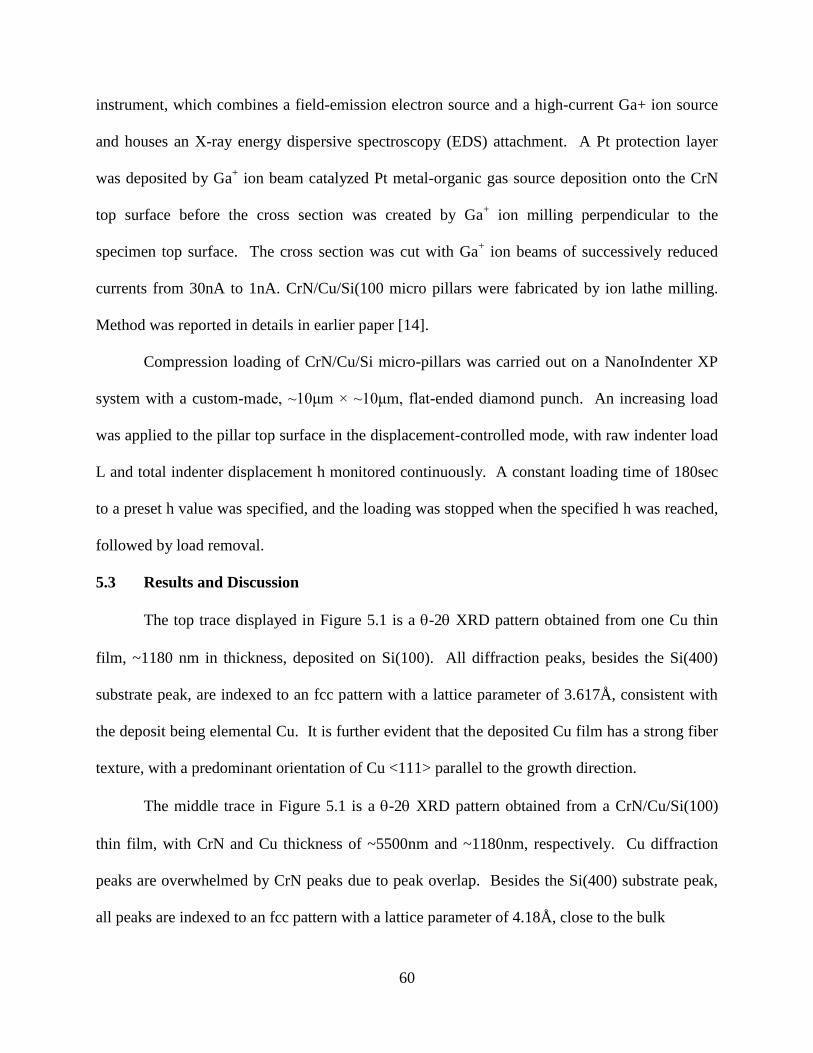
60
instrument, which combines a field-emission electron source and a high-current Ga+ ion source
and houses an X-ray energy dispersive spectroscopy (EDS) attachment. A Pt protection layer
was deposited by Ga+ ion beam catalyzed Pt metal-organic gas source deposition onto the CrN
top surface before the cross section was created by Ga+ ion milling perpendicular to the
specimen top surface. The cross section was cut with Ga+ ion beams of successively reduced
currents from 30nA to 1nA. CrN/Cu/Si(100 micro pillars were fabricated by ion lathe milling.
Method was reported in details in earlier paper [14].
Compression loading of CrN/Cu/Si micro-pillars was carried out on a NanoIndenter XP
system with a custom-made, ~10μm × ~10μm, flat-ended diamond punch. An increasing load
was applied to the pillar top surface in the displacement-controlled mode, with raw indenter load
L and total indenter displacement h monitored continuously. A constant loading time of 180sec
to a preset h value was specified, and the loading was stopped when the specified h was reached,
followed by load removal.
5.3 Results and Discussion
The top trace displayed in Figure 5.1 is a -2 XRD pattern obtained from one Cu thin
film, ~1180 nm in thickness, deposited on Si(100). All diffraction peaks, besides the Si(400)
substrate peak, are indexed to an fcc pattern with a lattice parameter of 3.617Å, consistent with
the deposit being elemental Cu. It is further evident that the deposited Cu film has a strong fiber
texture, with a predominant orientation of Cu <111> parallel to the growth direction.
The middle trace in Figure 5.1 is a -2 XRD pattern obtained from a CrN/Cu/Si(100)
thin film, with CrN and Cu thickness of ~5500nm and ~1180nm, respectively. Cu diffraction
peaks are overwhelmed by CrN peaks due to peak overlap. Besides the Si(400) substrate peak,
all peaks are indexed to an fcc pattern with a lattice parameter of 4.18Å, close to the bulk
61
Figure 5.1 X-ray diffraction characterization: (top trace) θ-2θ XRD pattern of a pure Cu film,
(middle trace) θ-2θ XRD pattern of a CrN/Cu/Si(100) film, (bottom trace) 2.5
glancing angle incidence diffraction pattern of the same CrN/Cu/Si(100) film.
B1-CrN lattice parameter of 4.149 Å and consistent with the top layer deposit being B1-CrN [17].
The XRD pattern also shows that the degree of texture within the CrN film is not as strong as the
Cu film, with the CrN<111> and CrN<200> directions being the main crystallographic directions
parallel to the growth direction. The bottom trace in Figure 5.1 shows a glancing incidence XRD
pattern obtained from the same CrN/Cu/Si(100) film, with a fixed incidence angle of 2.5. The
shallow incidence angle leads to a longer X-ray interaction path within CrN, and consequently a
higher number of more pronounced CrN diffraction peaks. Using the sin2 method [18] and
taking the lattice parameter, Young’s modulus, and Poisson’s ratio of CrN to be respectively
4.149Å, 200GPa, and 0.2, residual stress within the CrN film was obtained from the glancing
incidence data to be ~ 0.8GPa. Such a relatively low compressive residual stress level is
beneficial for depositing CrN films of higher thicknesses.
Figure 5.2 shows a FIB cross-section of a typical CrN/Cu/Si(100) specimen. The Pt
protection layer, the CrN layer, the Cu interlayer, and the Si substrate are clearly visible in the
62
cross-sectional SE image. The thickness of the Cu interlayer was measured from the cross
section to be ~550nm, with an estimated error of ~5% based on results of repeat measurements
Figure 5.2 A SE image of the FIB cross section of one CrN/Cu/Si(100) specimen. The inset
shows a titled plan-view SE image of the CrN top surface;
on the same specimen. The cross section reveals a dense and columnar structure of the CrN top
layer, typical of transition metal nitride films deposited with plasma or ion beam assist [19]. The
inset of Figure 5.2 shows a tilted plan-view of the CrN top layer surface in its as-deposited state.
The plan-view SE image shows surface roughness consistent with the columnar structure of the
CrN top layer as well as the absence of any perceptible voids, indicative of a fully dense film.
Similar procedures were used to measure the Cu interlayer thickness values in all CrN/Cu/Si(100)
specimens. Typical sizes of Cu grains were estimated by using the FIB cross section image,
where channeling of primary Ga+ ions enhances contrast between neighboring grains with
differing orientations. Lateral dimensions of Cu grains ranged from ~60nm to ~130nm with no
obvious dependence on film thickness, as expected from low temperature depositions.
The top trace displayed in Figure 5.3 is a survey spectrum obtained from a typical Cu thin
film. All observed spectral features can be assigned to various Cu core level transitions and
Auger transitions. At the binding energies corresponding respectively to O1s and C1s levels,
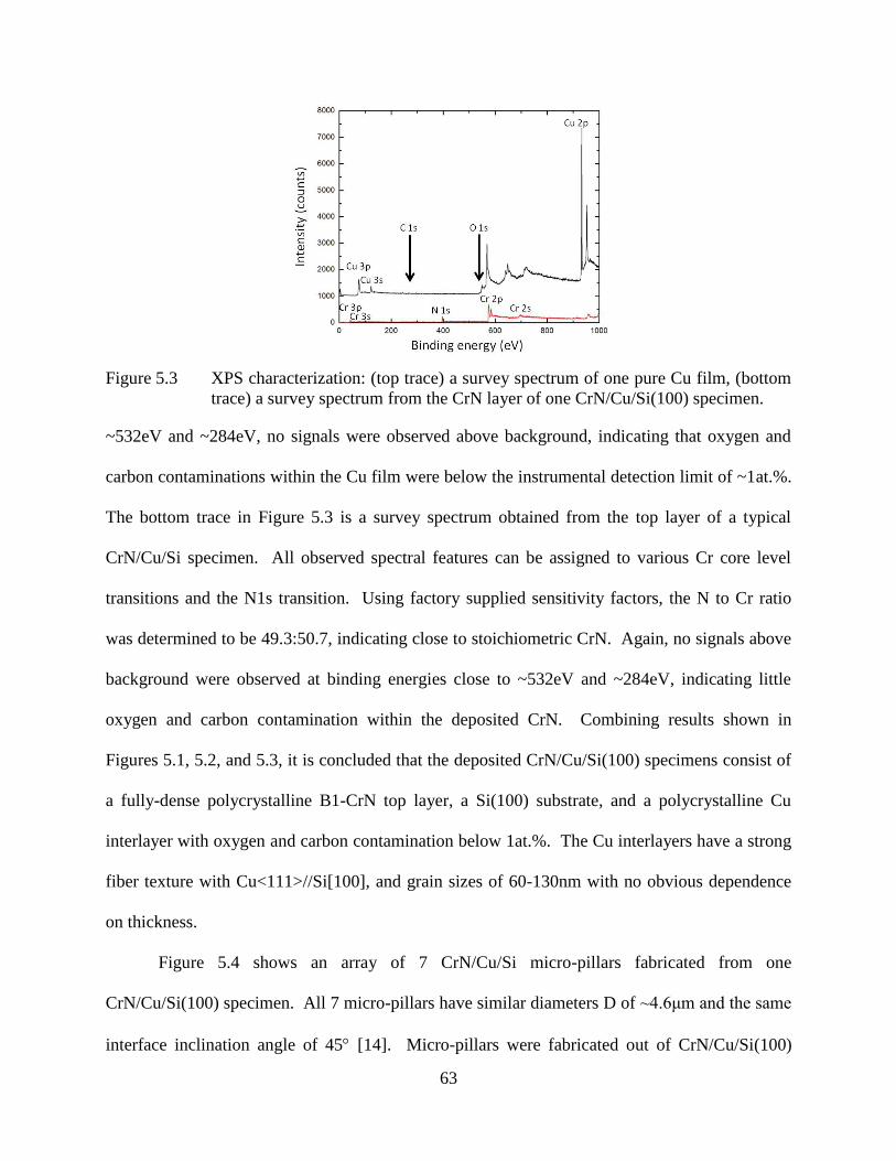
63
Figure 5.3 XPS characterization: (top trace) a survey spectrum of one pure Cu film, (bottom
trace) a survey spectrum from the CrN layer of one CrN/Cu/Si(100) specimen.
~532eV and ~284eV, no signals were observed above background, indicating that oxygen and
carbon contaminations within the Cu film were below the instrumental detection limit of ~1at.%.
The bottom trace in Figure 5.3 is a survey spectrum obtained from the top layer of a typical
CrN/Cu/Si specimen. All observed spectral features can be assigned to various Cr core level
transitions and the N1s transition. Using factory supplied sensitivity factors, the N to Cr ratio
was determined to be 49.3:50.7, indicating close to stoichiometric CrN. Again, no signals above
background were observed at binding energies close to ~532eV and ~284eV, indicating little
oxygen and carbon contamination within the deposited CrN. Combining results shown in
Figures 5.1, 5.2, and 5.3, it is concluded that the deposited CrN/Cu/Si(100) specimens consist of
a fully-dense polycrystalline B1-CrN top layer, a Si(100) substrate, and a polycrystalline Cu
interlayer with oxygen and carbon contamination below 1at.%. The Cu interlayers have a strong
fiber texture with Cu<111>//Si[100], and grain sizes of 60-130nm with no obvious dependence
on thickness.
Figure 5.4 shows an array of 7 CrN/Cu/Si micro-pillars fabricated from one
CrN/Cu/Si(100) specimen. All 7 micro-pillars have similar diameters D of ~4.6μm and the same
interface inclination angle of 45 [14]. Micro-pillars were fabricated out of CrN/Cu/Si(100)

64
specimens with different t values. In all cases, the minimum distance between the CrN/Cu/Si
interface and the pillar top surface was 2µm, and the ratio t/D was <0.20.
Figure 5.4 An ISE image of an array of CrN/Cu/Si(100) micro-pillars after FIB lathe-milling
Figure 5.5 shows a collection of raw L-h curves measured from five groups of micro-
pillar specimens, with t values of ~150nm, ~340nm, ~550nm, ~810nm, and ~1180nm,
Figure 5.5 Raw L-h curves obtained from compression loading of CrN/Cu/Si(100) micro-
pillars with 45°-inclined interfaces. Five groups of data were obtained from
pillars with five t values.
respectively. Within each specimen group, repeat measurements on 4 to 6 separate micro-pillars
were conducted. Several features are evident. First, all L-h curves exhibit a rapid,
approximately linear, increase in L with increasing h until a critical L value, Lc, is reached.
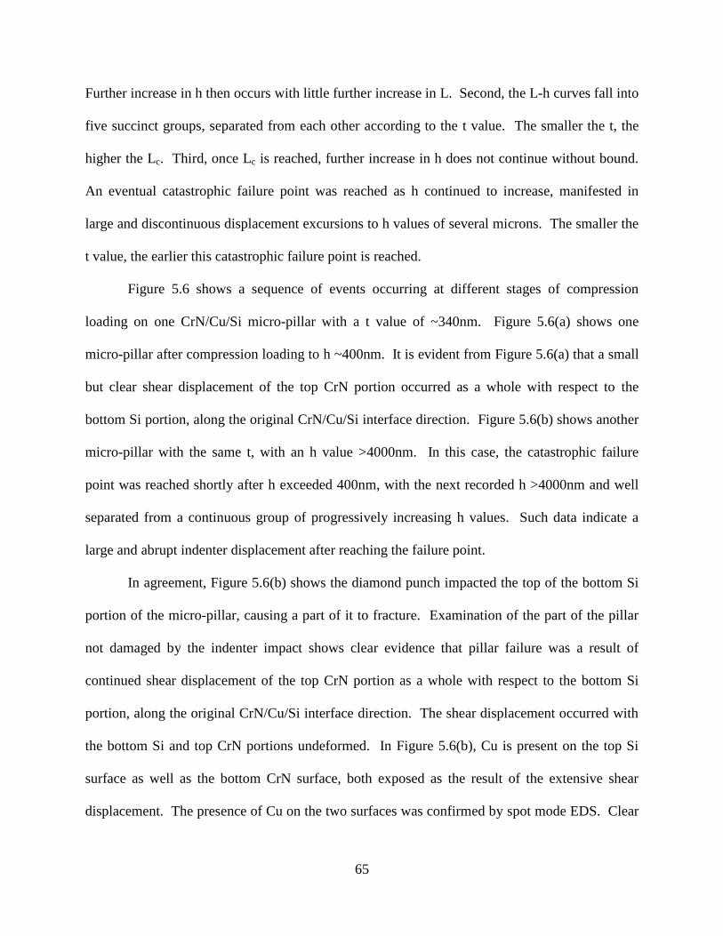
65
Further increase in h then occurs with little further increase in L. Second, the L-h curves fall into
five succinct groups, separated from each other according to the t value. The smaller the t, the
higher the Lc. Third, once Lc is reached, further increase in h does not continue without bound.
An eventual catastrophic failure point was reached as h continued to increase, manifested in
large and discontinuous displacement excursions to h values of several microns. The smaller the
t value, the earlier this catastrophic failure point is reached.
Figure 5.6 shows a sequence of events occurring at different stages of compression
loading on one CrN/Cu/Si micro-pillar with a t value of ~340nm. Figure 5.6(a) shows one
micro-pillar after compression loading to h ~400nm. It is evident from Figure 5.6(a) that a small
but clear shear displacement of the top CrN portion occurred as a whole with respect to the
bottom Si portion, along the original CrN/Cu/Si interface direction. Figure 5.6(b) shows another
micro-pillar with the same t, with an h value >4000nm. In this case, the catastrophic failure
point was reached shortly after h exceeded 400nm, with the next recorded h >4000nm and well
separated from a continuous group of progressively increasing h values. Such data indicate a
large and abrupt indenter displacement after reaching the failure point.
In agreement, Figure 5.6(b) shows the diamond punch impacted the top of the bottom Si
portion of the micro-pillar, causing a part of it to fracture. Examination of the part of the pillar
not damaged by the indenter impact shows clear evidence that pillar failure was a result of
continued shear displacement of the top CrN portion as a whole with respect to the bottom Si
portion, along the original CrN/Cu/Si interface direction. The shear displacement occurred with
the bottom Si and top CrN portions undeformed. In Figure 5.6(b), Cu is present on the top Si
surface as well as the bottom CrN surface, both exposed as the result of the extensive shear
displacement. The presence of Cu on the two surfaces was confirmed by spot mode EDS. Clear
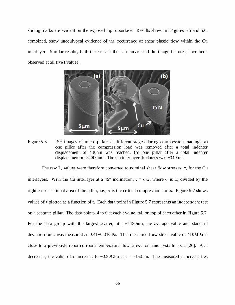
66
sliding marks are evident on the exposed top Si surface. Results shown in Figures 5.5 and 5.6,
combined, show unequivocal evidence of the occurrence of shear plastic flow within the Cu
interlayer. Similar results, both in terms of the L-h curves and the image features, have been
observed at all five t values.
Figure 5.6 ISE images of micro-pillars at different stages during compression loading: (a)
one pillar after the compression load was removed after a total indenter
displacement of 400nm was reached, (b) one pillar after a total indenter
displacement of >4000nm. The Cu interlayer thickness was ~340nm.
The raw Lc values were therefore converted to nominal shear flow stresses, , for the Cu
interlayers. With the Cu interlayer at a 45 inclination, = /2, where is Lc divided by the
right cross-sectional area of the pillar, i.e., is the critical compression stress. Figure 5.7 shows
values of plotted as a function of t. Each data point in Figure 5.7 represents an independent test
on a separate pillar. The data points, 4 to 6 at each t value, fall on top of each other in Figure 5.7.
For the data group with the largest scatter, at t ~1180nm, the average value and standard
deviation for was measured as 0.41±0.01GPa. This measured flow stress value of 410MPa is
close to a previously reported room temperature flow stress for nanocrystalline Cu [20]. As t
decreases, the value of increases to ~0.80GPa at t = ~150nm. The measured increase lies
67
significantly outside the range of data scatter, showing a clear dependence of on t in confined
shear plastic flow. To our knowledge, this is the first time such dependence has been measured
Figure 5.7 Values of the nominal shear flow stress of Cu interlayers as a function of the
interlayer thickness.
unequivocally. Separate measurements showed that the critical compression stress did not
exhibit a strong dependence on the pillar diameter. For a given Cu interlayer thickness, the
difference in the critical compression stress was measured to be <10% as the pillar diameter
varied between ~5μm to ~2μm.
Ideal shear strength of single crystal Si has been reported to be ~7GPa [21]. The
hardness of CrN has been measured to be >20GPa [12]. Given that values presently measured
were <2GPa, the fact that both Si and CrN remained undeformed during compression loading is
expected. Direct comparison between data presented in Figure 5.7 and non-local plasticity
theories are complicated by several factors. One is that the Cu interlayers presently studied are
polycrystalline with small grain sizes. Even though the predominance of Cu grains are oriented
with the {111} slip plane parallel to the shear direction, the presence of numerous grain
boundaries within the shear plane presents a more complicated situation as compared to previous
simulations [4-8]. Another is that, instead of a perfectly flat interface, the CrN/Cu interface
68
contains sub-micron scale roughness resulting from the columnar structure of the CrN top layer.
The presence of such roughness is manifested in the sliding marks shown in Figure 5.6(b), when
the shear plastic flow is occurring close to the CrN/Cu interface. Experimental efforts to better
control such complications, e.g., by controlling the grain size of the metal interlayer, are ongoing.
In summary, compression loading of CrN/Cu/Si(100) micro-pillars containing inclined
interfaces yielded unequivocal evidence of shear plastic flow within polycrystalline Cu thin films
confined between undeforming single crystal Si(100) and polycrystalline CrN. A clear and
significant dependence of the shear flow stress on Cu layer thickness was demonstrated. The
present results give a new and independent measure of the size effects in confined shear plastic
flow. It is hoped that the presently described shear test will just be the beginning of experimental
efforts to generate more data on this fundamental problem.
5.4 References
[1] N.A. Fleck, G.M. Muller, M.F. Ashby, J.W. Hutchinson, Strain gradient plasticity: theory
and experiment, Acta Metall. Mater. 42, 475-487 (1994).
[2] Q. Ma, D.R. Clarke, Size dependent hardness of silver single crystals, J. Mater. Res. 10,
853-863 (1995).
[3] J.S. Stolken, A.G. Evans, A microbend test method for measuring the plasticity length
scale, Acta Mater. 46, 5109–5115 (1998).
[4] N.A. Fleck, J.W. Hutchinson, Strain gradient plasticity, Adv. Appl. Mech. 33, 295-361
(1997).
[5] J.Y. Shu, N.A. Fleck, E. Van der Giessen, A. Needleman, Boundary layers in constrained
plastic flow: comparison of nonlocal and discrete dislocation plasticity, J. Mech. Phys.
Solids 49, 1361-1395 (2001).
[6] E. Bittencourt, A. Needleman, M.E. Gurtin, E. Van der Giessen, A comparison of
nonlocal continuum and discrete dislocation plasticity predictions, J. Mech. Phys. Solids
51(2), 281-310 (2003).
[7] P. Fredriksson, P. Gudmundson, Size-dependent yield strength of thin films, Int. J.
Plasticity 21(9), 1834-1854 (2005).
69
[8] S.P. Lele, L. Anand, A small-deformation strain-gradient theory for isotropic viscoplastic
materials, Phil. Mag. 88(30-32), 3655-3689 (2008).
[9] V.L. Tagarielli, N.A. Fleck, The shear response of a thin aluminum layer, J. Appl. Mech.
78, 014505/1-3 (2011).
[10] M. Eckels, M.N. Kotzalas, G.L. Doll, Attaining high levels of bearing performance with
a nanocomposite diamond-like carbon coating, Tribology Transactions 56, 410-416
(2013).
[11] D.M. Cao, W.J. Meng, Microscale compression molding of Al with surface engineered
LiGA inserts, Microsyst. Technol. 10, 662-670 (2004).
[12] D.C. Agrawal, R. Raj, Measurement of the ultimate shear strength of a metal-ceramic
interface, Acta Metall. 37, 1265-1270 (1989).
[13] R. Saha, W.D. Nix, Effects of the substrate on the determination of thin film mechanical
properties by nanoindentation, Acta Mater. 50, 23-38 (2002).
[14] K. Chen, Y. Mu, W.J. Meng, A new experimental approach for evaluating the mechanical
integrity of interfaces between hard coatings and substrates, MRS Comm. 4, 19-23 (2014).
[15] P.A. Shade, R. Wheeler, Y.S. Choi, M.D. Uchic, D.M. Dimiduk, H.L. Fraser, A
combined experimental simulation study to examine lateral constraint effects on micro-
compression of single slip oriented single crystals, Acta Mater. 67, 4580-4587 (2009).
[16] W.J. Meng, T.J. Curtis, L.E. Rehn, P.M. Baldo, Temperature dependence of inductively
coupled plasma assisted deposition of titanium nitride coatings, Surf. Coat. Technol.
120/121, 206-212 (1999).
[17] L.E. Toth, Transition Metal Carbides and Nitrides, Academic Press, New York, 1971.
[18] A. J. Perry, J. A. Sue, P. J. Martin, Practical measurement of the residual stress in
coatings, Surf. Coat. Technol. 81, 17-28 (1996).
[19] T. Itoh (Editor), Ion Beam Assisted Film Growth, Elsevier, Amsterdam, 1989.
[20] T. Kunimine, N. Takata, N. Tsuji, T. Fujii M. Kato, S. Onaka, Temperature and strain
rate dependence of flow stress in severely deformed copper by accumulative roll bonding,
Mater. Trans. 50, 64-69 (2009).
[21] D. Roundy, M.L. Cohen, Ideal strength of diamond, Si, and Ge, Phys. Rev. B 64,
212103/1-3 (2001).
70
CHAPTER 6
MICRO-PILLAR MEASUREMENT OF PLASTICITY IN CONFINED CU THIN FILMS
6.1 Introduction
In the last two decades, the dominant experimental means for affecting plastic flow in
small volumes, including in thin metal films, has been instrumented micro- and nano-indentation.
A methodology for extracting hardness values from experimentally obtained load-displacement
curves has been established and well accepted [1]. In particular, a principal avenue through
which length scale dependent plasticity effects are demonstrated experimentally has been
through the indentation size effect [2]. However, for measuring plastic flow in thin films,
substrate influence complicates the determination of the mechanical flow strength using
indentation [3, 4].
We recently demonstrated a new experimental protocol for evaluating the mechanical
integrity of interfaces between hard coatings and substrates [5]. Vapor deposited specimens in
the configuration of coating/interlayer/substrate were fabricated via scripted focused ion beam
(FIB) milling into microscale cylindrical pillars, with interfaces at a pre-determined inclination
angle with respect to the pillar axis. Axial compression loading of the pillars then resulted in
interfacial failures, providing a quantitative measurement of the critical failure stress [5]. When
the coating and the substrate are both elastic-brittle materials, such as CrN and Si, and the
interlayer is a metal, such as Cu, axial compression of micro-pillars with inclined interfaces
results in a combination of compressive and shear stress acting on the interlayer. Furthermore,
with well bonded interfaces, extensive plastic shearing of thin polycrystalline Cu interlayers was
observed, together with a significant dependence of the shear flow stress on the Cu thickness [6].
Shearing of a metal layer bonded between two non-deforming substrates is the iconic
example that illustrates the connection between gradients of plastic strain and enhanced flow
71
strength. Due to its analytical simplicity, the confined shear problem has been widely considered
as an example in the development of continuum strain gradient plasticity (SGP) and discrete
dislocation plasticity (DDP) theories [7,8,9,10,11]. Normal compression of a finite width metal
layer bonded between rigid platens has also been considered as an application of SGP theories
[12]. Normal compression of a metal thin film bonded to platens was suggested as a useful
loading geometry for measuring the material length parameter underlying the size effect,
especially if companion shear data are available [12]. The micro-pillar experimental technique
described in [5] and [6] creates such a possibility of conducting normal compression and shear
tests on the same metal thin film.
In this paper, we report results of axial compression testing on CrN/Cu/Si(100) micro-
pillars, with interfaces either perpendicular to the pillar axial direction or at a 45 inclination.
Compression testing of the micro-pillars has been performed on an instrumented nanoindenter
with a flat punch at different pillar diameters, D , Cu interlayer thicknesses, h , and over a range
of indenter displacements, d .
6.2 Deposition and Structural Characterization of Polycrystalline CrN and Cu Thin
Films
Cu and CrN thin films were vapor phase deposited onto 50mm diameter Si(001) wafers
in an ultra-high-vacuum (UHV) deposition tool in a load-locked configuration. The deposition
chamber housed a 13.56MHz inductively coupled plasma (ICP). Four balanced magnetron
sputter sources, accepting 75mm diameter sputter targets, faced the center of the deposition
chamber. The base pressure of the deposition chamber was ~3×10⁻⁹
Torr [13,14,15]. Cleaned
Si(001) substrates were evacuated to 3×10⁻⁷
Torr in the load lock and then transferred to a
holder placed at the center of the UHV deposition chamber. One elemental Cu (99.99%) target
and three elemental Cr targets (99.95%) were used, all operated in the dc current-controlled
72
mode. Deposition of Cu thin films occurred in ~10mTorr of pure Ar (99.999%+). Deposition of
CrN thin films occurred in ~10mTorr of Ar/N2 (99.999%+/99.999%+) mixture. Prior to
deposition, Si substrates were subjected to an Ar ICP etch for ~5min at a bias voltage of -50V.
All depositions occurred without intentional substrate heating.
A series of single-layer Cu thin films were deposited onto Si(001) substrates. Cu
deposition occurred with the sputter source operated at 1.0A, and with an Ar ICP assist at a total
ICP input power of 1000W. A substrate bias of -50V was applied during deposition. The Cu
film thickness was controlled through the deposition time. Another series of bilayer CrN/Cu thin
films were deposited onto Si(001) substrates. Cu interlayers were first deposited onto Si(001) in
pure Ar with ICP assist, followed immediately by deposition of CrN top layers in an Ar/N2
mixture, also with ICP assist at a total ICP input power of 1000W. During CrN deposition, a
substrate bias of -100V was applied. To ensure CrN deposition at close to stoichiometry, the
input N2 flow was kept above the pressure hysteresis point.
Morphological characterization of the Cu/Si(001) and CrN/Cu/Si(001) specimens was
carried out by scanning electron microscopy (SEM) on a FEI Quanta3D FEG focused ion beam
(FIB) instrument with an X-ray energy dispersive spectroscopy (EDS) attachment. The FIB
instrument combines a field-emission electron source and a high-current Ga+ ion source, and
enables scanning images taken in either the electron-induced secondary electron (SE) mode or
the ion-induced secondary electron (ISE) mode.
Typical results of morphological observation from CrN/Cu/Si(001) specimens are
illustrated in Figure 6.1. Figure 6.1(a) shows an SE image of a cross section perpendicular to the
original specimen surface, created by Ga+ ion milling. A Pt protection layer was laid on top of
the specimen surface prior to ion milling by Ga+ catalyzed deposition from an organometallic Pt
73
precursor. Figure 6.1(a) shows in sequence the Pt protection layer, the CrN top layer, the Cu
interlayer, and the Si substrate. The thicknesses of the CrN and Cu layers were measured
respectively to be ~5.5m and ~810nm, with typical scatter of ±5% based on repeat
measurements. Figure 6.1(b) shows a plan-view SE image of the as-deposited CrN top surface,
with surface roughness typical of vapor deposited polycrystalline columnar refractory ceramics.
Both the cross section and the plan-view images indicate that the CrN top layer is fully dense.
Figure 6.1. FIB examination of a typical CrN/Cu/Si specimen: (a) A cross sectional SE image;
(b) a 52 tilted plan-view SE image.
Compositional characterization of the Cu/Si(100) and CrN/Cu/Si(001) specimens was
carried out by X-ray photoelectron spectroscopy (XPS) on a Kratos AXIS165 spectrometer with
monochromatic Al Kα excitation. Composition quantification was obtained from raw XPS
spectra using factory supplied sensitivity factors. Prior to XPS spectra collection, the specimen
surface was sputter cleaned with an Ar+ ion beam for ~20min, with the Ar
+ ion beam set at 4kV
and 15mA.
Figure 6.2 shows XPS survey spectra collected from top layers of a typical Cu/Si
specimen and a typical CrN/Cu/Si specimen. The Cu spectrum shows peaks consistent with

74
Cu3p, Cu3s, and Cu2p emissions. Signal at the O1s and C1s positions, at binding energies of
532eV and 284eV, is not above the noise level. The CrN spectrum shows peaks consistent with
Cr3p, Cr3s, Cr2p, Cr2s, and N1s emissions. Signal at the O1s and C1s positions is also not
above the noise level. The Cr:N ratio is determined to be 51:49. XPS data thus show that the Cu
layers consist of elemental Cu, and that the CrN layers consist of Cr and N at close to the
stoichiometric ratio. The O and C impurity levels in both Cu and CrN layers are below the XPS
detection limit of ~1at.%.
Figure 6.2 XPS survey spectra collected from top layers of a typical Cu/Si specimen and a
typical CrN/Cu/Si specimen. In both cases, the oxygen impurity level is at or
below the XPS detection limit of ~1 at.%.
Structural characterization of Cu and CrN thin films was carried out by X-ray diffraction
(XRD) on a PANalytical Empyrean system. Diffraction patterns were obtained using CuKα
radiation with specimens mounted on a χ-φ-x-y-z stage. Diffraction patterns in the glancing
incidence geometry, the symmetric -2 geometry, and the -rocking curve geometry are
75
obtained with an incident beam graphite mirror and a Pixel3D detector. X-ray pole figure data
were obtained with an incident beam double-cross slit and a scintillation detector.
Results of XRD characterization of the structure of CrN layers in CrN/Cu/Si(001)
specimens are illustrated by data shown in Figure 6.3. The glancing incidence XRD pattern,
shown in Figure 6.3(a), collected from one typical CrN/Cu/Si(001) specimen at an beam
incidence angle =2.5, shows diffraction peaks only from the CrN top layer. All diffraction
Figure 6.3 XRD examination of a typical CrN/Cu/Si(001) specimen: (a) glancing incidence
(=2.5°) diffraction pattern; (b) θ-2θ diffraction pattern; (c) sin2Ψ analysis of the
glancing incidence data shown in (a)
peaks can be indexed to a cubic structure with lattice parameter a = 4.18Å, close to the bulk B1-
CrN lattice parameter of 4.15Å [16]. The -2 XRD pattern, shown in Figure 6.3(b) and
collected from the same specimen, shows the Si(004) diffraction peak from the Si substrate and
76
one minor Cu(220) diffraction peak from the Cu interlayer in addition to all diffraction
peaksindexed to B1-CrN, with a = 4.18Å. Taken together, glancing incidence and -2 XRD
data are consistent with the CrN film having the B1-NaCl structure, being polycrystalline, and
with preferential alignment of CrN<111> and CrN<200> along Si[001], the growth direction.
The level of residual stress within the CrN top layer was estimated from analysis of the
glancing incidence XRD data shown in Figure 6.3(a). When the X-ray incidence angle was fixed
at =2.5 and the detector was scanned to obtain diffraction signals in the range of 20 < 2 <
120, the angle between the scattering vector k
and the specimen surface normal n
, , is given
by [17]. The CrN lattice parameter, aCrN, was calculated from the multitude of B1-
CrN diffraction peaks shown in Figure 6.3(a), and plotted versus sin2 in Figure 6.3(c).
Assuming an equal biaxial residual stress R existing within the CrN layer, the variation of aCrN
as the angle varies relates in the following way to R [17,18]:
oRoR aE
aE
a
21sin
1 2. (6.1)
In Equation 6.1, E and are respectively the Young’s modulus and Poisson’s ratio of the CrN
layer, and ao is the bulk lattice parameter of CrN. A linear least squares fit to the data shown in
Figure 6.3(c) yielded a slope of -0.022±0.017Å and an intercept of 4.187±0.007 Å. The negative
slope of the 2sin plot indicates that the residual stress within CrN is compressive.
Independent of the values of E and , the fact that the slope uncertainty is comparable to the
slope itself indicate that the level of residual stress is moderate. Values of E for CrN reported in
the literature vary widely from ~200GPa to above 400GPa [19,20]. Taking ao to be 4.15 Å, to
be 0.2 [21], and E to be 400GPa [22], the fitted slope of the 2sin plot yields R = -1.8±1.4GPa.
It is noted that, since E = 400GPa is a high value for CrN, this R value represents an upper bond
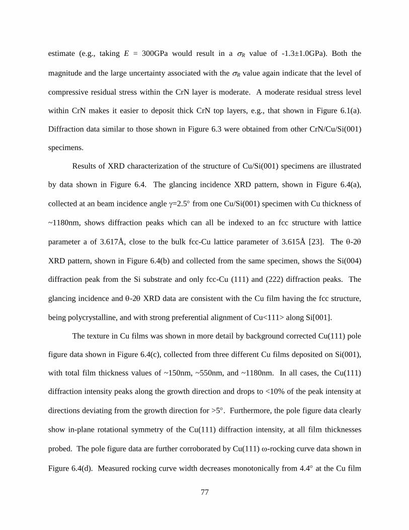
77
estimate (e.g., taking E = 300GPa would result in a R value of -1.3±1.0GPa). Both the
magnitude and the large uncertainty associated with the R value again indicate that the level of
compressive residual stress within the CrN layer is moderate. A moderate residual stress level
within CrN makes it easier to deposit thick CrN top layers, e.g., that shown in Figure 6.1(a).
Diffraction data similar to those shown in Figure 6.3 were obtained from other CrN/Cu/Si(001)
specimens.
Results of XRD characterization of the structure of Cu/Si(001) specimens are illustrated
by data shown in Figure 6.4. The glancing incidence XRD pattern, shown in Figure 6.4(a),
collected at an beam incidence angle =2.5 from one Cu/Si(001) specimen with Cu thickness of
~1180nm, shows diffraction peaks which can all be indexed to an fcc structure with lattice
parameter a of 3.617Å, close to the bulk fcc-Cu lattice parameter of 3.615Å [23]. The -2
XRD pattern, shown in Figure 6.4(b) and collected from the same specimen, shows the Si(004)
diffraction peak from the Si substrate and only fcc-Cu (111) and (222) diffraction peaks. The
glancing incidence and -2 XRD data are consistent with the Cu film having the fcc structure,
being polycrystalline, and with strong preferential alignment of Cu<111> along Si[001].
The texture in Cu films was shown in more detail by background corrected Cu(111) pole
figure data shown in Figure 6.4(c), collected from three different Cu films deposited on Si(001),
with total film thickness values of ~150nm, ~550nm, and ~1180nm. In all cases, the Cu(111)
diffraction intensity peaks along the growth direction and drops to <10% of the peak intensity at
directions deviating from the growth direction for >5. Furthermore, the pole figure data clearly
show in-plane rotational symmetry of the Cu(111) diffraction intensity, at all film thicknesses
probed. The pole figure data are further corroborated by Cu(111) -rocking curve data shown in
Figure 6.4(d). Measured rocking curve width decreases monotonically from 4.4 at the Cu film

78
thickness of ~150nm to 3.0 at ~550nm and to 2.4 at ~1180nm. Taken together, X-ray
diffraction data shown in Figure 6.4 indicate that the Cu films are fcc in structure and have
almost perfect fiber texture with Cu<111> along Si[001] to within a few degrees. The Cu films
are polycrystalline with random in-plane orientation.
Figure 6.4 XRD examination of a typical Cu/Si(001) specimen with a cu film thickness of
~1180nm: (a) glancing incidence (=2.5°) diffraction pattern; (b) θ-2θ diffraction
pattern; (c) background corrected Cu(111) pole figures from three polycrystalline
Cu layers on Si(001), the Cu film thickness values are indicated on top of the pole
figures; (d) Cu<111> rocking curves from three polycrystalline Cu layers on
Si(001), the Cu film thickness values are indicated on top of the curve
Grain structure of CrN and Cu thin films was further characterized by transmission
electron microscopy (TEM), carried out on a JEOL JEM2011 microscope operated at 200kV.
Cross-sectional TEM specimens were made from sputter deposited thin films by Ga+ ion
sectioning into rectangular sections, lift-out using an in-situ OmniProbe, gluing by Ga+ catalyzed
Pt deposition onto a TEM grid, followed by Ga+ ion thinning at 30kV and 5kV. Final specimen

79
thinning/cleaning was performed on a Gatan PIPS II ion polishing system using an Ar+ ion beam
at 500eV or less. Further details regarding Ga+ ion beam sectioning and TEM specimen lift-out
have been described elsewhere [24]. Additional TEM specimens were made without the final
Ar+ ion thinning/cleaning step. With respect to characterizing the grain structure, no significant
difference was found between specimens with or without the final low energy Ar+
thinning/cleaning step.
A cross-sectional TEM bright-field (BF) image, shown in Figure 6.5(a), was obtained
from the CrN/Cu/Si(001) specimen whose morphology was shown in Figure 6.1. The specimen
was oriented with the Si substrate in the [110] zone axis direction. Both CrN and Cu layers are
polycrystalline. Both CrN/Cu and Cu/Si interfaces appear clean, without indication of extensive
interdiffusion and reaction. For this specimen, the Cu interlayer thickness was measured from
Figure 6.5(a) to be ~810nm, which was consistent with the value measured by FIB cross
sectioning in Figure 6.1(a). Figure 6.5(b) shows selected area diffraction patterns (SADPs)
obtained respectively from the CrN top layer, the Cu interlayer, and the Si substrate areas. The
SADP from Si shows the Si[110] zone axis diffraction pattern. The SADPs from Cu and CrN are
consistent with the structure of Cu being fcc and that of CrN being B1-NaCl. Figure 6.6 shows a
typical TEM bright-field/dark-field (BF/DF) image pair of the CrN top layer near the CrN/Cu
interface. The CrN layer has a pronounced columnar structure, with columns with widths ~50nm
and large length/width ratios. The columnar structure of CrN shown in cross sectional TEM is
consistent with the rough surface morphology observed in Figure 6.1. The CrN layer appears
fully dense, without indication of inter-columnar voids. Figure 6.7 shows a typical TEM BF/DF
image pair of the Cu interlayer near the Cu/Si interface. The Cu layer consists of a random
mixture of columnar and near equi-axed grains. The presence of nano-twins within the columnar

80
Figure 6.5 Cross sectional TEM examination of a typical CrN/Cu/Si(001) specimen: (a) A
cross sectional BF image across the entire Cu interlayer. The CrN/Cu and Cu/Si
interfaces are indicated by white arrows; (b) typical SAED patterns collected
from the (left to right) CrN, Cu and Si layer.
Figure 6.6 Cross sectional TEM examination of the CrN top layer: (a) A BF image, (b) A DF
image. White arrows indicate the location of the CrN/Cu interface
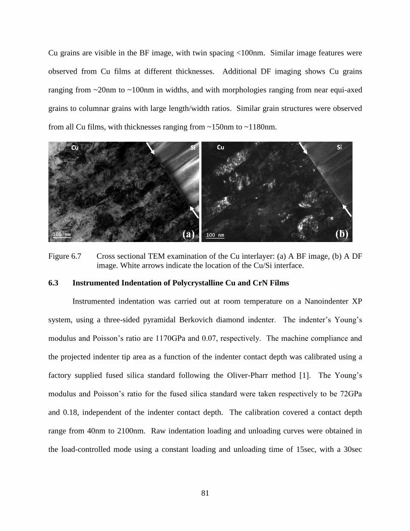
81
Cu grains are visible in the BF image, with twin spacing <100nm. Similar image features were
observed from Cu films at different thicknesses. Additional DF imaging shows Cu grains
ranging from ~20nm to ~100nm in widths, and with morphologies ranging from near equi-axed
grains to columnar grains with large length/width ratios. Similar grain structures were observed
from all Cu films, with thicknesses ranging from ~150nm to ~1180nm.
Figure 6.7 Cross sectional TEM examination of the Cu interlayer: (a) A BF image, (b) A DF
image. White arrows indicate the location of the Cu/Si interface.
6.3 Instrumented Indentation of Polycrystalline Cu and CrN Films
Instrumented indentation was carried out at room temperature on a Nanoindenter XP
system, using a three-sided pyramidal Berkovich diamond indenter. The indenter’s Young’s
modulus and Poisson’s ratio are 1170GPa and 0.07, respectively. The machine compliance and
the projected indenter tip area as a function of the indenter contact depth was calibrated using a
factory supplied fused silica standard following the Oliver-Pharr method [1]. The Young’s
modulus and Poisson’s ratio for the fused silica standard were taken respectively to be 72GPa
and 0.18, independent of the indenter contact depth. The calibration covered a contact depth
range from 40nm to 2100nm. Raw indentation loading and unloading curves were obtained in
the load-controlled mode using a constant loading and unloading time of 15sec, with a 30sec

82
load hold at the maximum load, Lmax. Multiple load vs. indenter displacement, L-d, curves were
obtained at one dmax value, and dmax was varied to obtain a complete set of indentation data.
Figure 6.8 displays indentation results obtained from a Cu/Si(001) specimen, with a Cu
film thickness of ~1180nm. Figure 6.8(a) shows values of measured indentation modulus, Eind =
E/(1-2), as a function of the indenter contact depth. Error bars for the modulus value are
Figure 6.8 Instrumented indentation of a Cu/Si(001) specimen with a Cu thickness of
~1180nm: (a) indentation modulus vs. contact depth, (b) hardness vs. contact
depth
derived from repeat L-d curves at the same dmax value. In the absence of an independent
measurement on the Poisson’s ratio, only Eind can be obtained from the elastic unloading portion
of the indentation curve. Figure 6.8(a) shows that Eind increase slightly from ~150GPa at large
contact depths to ~170GPa at contact depths between 200nm to 350nm.
The elastic stiffness constants for fcc Cu are respectively C11 = 168.4GPa, C12 =
121.4GPa, and C44 = 75.4GPa [25], and those for diamond-cubic Si are respectively C11 =
165.6GPa, C12 = 63.9GPa, and C44 = 79.5GPa [26]. The elastic compliance constants for Cu are
respectively S11 = 14.99(TPa)-1
, S12 = -6.28(TPa)-1
, and S44 = 13.26(TPa)-1
, and those for Si are
respectively S11 = 7.69(TPa)-1
, S12 = -2.14(TPa)-1
, and S44 = 12.58(TPa)-1
[26]. Young’s
83
modulus in the <001> and <111> directions of cubic crystals are obtained from the compliance
constants as [27],
1
11100
sE , (6.1)
1
441211111112
1
3
2
ssssE . (6.2)
For Cu, E100 and E111 are respectively 67GPa and 191GPa. For Si, E100 and E111 are respectively
130GPa and 188GPa. Furthermore, Poisson’s ratio in the <hkl> direction of cubic crystals are
given by [28]
)2(22
1
1211 CC
Ehklhkl
. (6.3)
For Cu, 100 and 111 are respectively 0.42 and 0.27. For Si, 100 and 111 are respectively 0.28
and 0.18. In the <001> and <111> directions, the Cu indentation modulus takes on respectively
values of 81GPa and 206GPa and the Si indentation modulus takes on respectively values of
141GPa and 194GPa. Based on the XRD results shown in Figure 6.4, the relevant indentation
moduli for indentation on the present Cu/Si(001) specimens should respectively be Eind(111) =
206GPa for the Cu film and Eind(001) = 141GPa for the Si substrate, i.e., the Cu/Si specimen
goes from an elastically stiffer film to an elastically more compliant substrate. Thus the data
shown in Figure 6.8(a) is trend-wise consistent with what is expected based on the predominant
fiber texture of the Cu films, with Cu<111>//Si[001]. Measured Eind value is close to Eind for the
Si substrate at large contact depths.
Figure 6.8(b) shows values of measured hardness as a function of the indenter contact
depth. Error bars for the hardness value are derived from repeat L-d curves at the same dmax
value. Measured hardness values decrease from above 4GPa at large contact depths to ~3GPa at
contact depths between 200nm to 350nm. The indentation hardness of Si at room temperature is
84
~10GPa, limited by a pressure-induced phase transformation [29]. The Cu/Si specimen goes
from a softer film to a harder substrate. Thus the observed decrease in hardness with decreasing
contact depth is again qualitatively consistent with expectation. Caution should be exercised in
taking the measured hardness value of ~3GPa at small contact depths as an “intrinsic” hardness
of the Cu film, for it is influenced by two extra factors: one being the effect of a harder Si
substrate and the other being the expected presence of an indentation size effect. Both effects
tend to elevate measured hardness values. For these reasons, indentations on Cu/Si specimens
with smaller Cu film thicknesses were not performed.
Figure 6.9 displays indentation results obtained from a 6.2m thick polycrystalline CrN
film deposited on Si(001), over a range of indenter contact depth from ~1400nm to ~370nm.
Figure 6.9(a) shows that the indentation modulus increases monotonically with decreasing
indenter contact depth, to ~275GPa at the smallest contact depth of ~370nm. The observed trend
is consistent with the expectation for an elastically stiffer film on an elastically more compliance
substrate, where measured indentation modulus decreases monotonically with increasing
indenter contact depth [30]. A simple extrapolation of the data shown in Figure 6.9(a) suggests
that the indentation modulus of the present CrN film is ~300GPa. Figure 6.9(b) shows that
measured hardness values in the same contact depth range exhibit only a modest change, from
~16GPa to ~18GPa. Noting that values of indenter contact depth normalized to the CrN film
thickness range from 0.06 to 0.23, a simple average of all hardness values shown in Figure 6.9(b)
yield a hardness value of ~17GPa, a value believed to be representative of the presently
deposited CrN films.
Values of Young’s modulus for CrN as reported in the literature vary widely, from
190GPa to above 400GPa [22,20]. Moduli of sputter deposited CrN films are often reported to
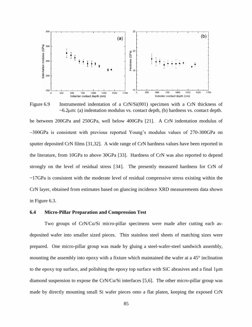
85
Figure 6.9 Instrumented indentation of a CrN/Si(001) specimen with a CrN thickness of
~6.2m: (a) indentation modulus vs. contact depth, (b) hardness vs. contact depth.
be between 200GPa and 250GPa, well below 400GPa [21]. A CrN indentation modulus of
~300GPa is consistent with previous reported Young’s modulus values of 270-300GPa on
sputter deposited CrN films [31,32]. A wide range of CrN hardness values have been reported in
the literature, from 10GPa to above 30GPa [33]. Hardness of CrN was also reported to depend
strongly on the level of residual stress [34]. The presently measured hardness for CrN of
~17GPa is consistent with the moderate level of residual compressive stress existing within the
CrN layer, obtained from estimates based on glancing incidence XRD measurements data shown
in Figure 6.3.
6.4 Micro-Pillar Preparation and Compression Test
Two groups of CrN/Cu/Si micro-pillar specimens were made after cutting each as-
deposited wafer into smaller sized pieces. Thin stainless steel sheets of matching sizes were
prepared. One micro-pillar group was made by gluing a steel-wafer-steel sandwich assembly,
mounting the assembly into epoxy with a fixture which maintained the wafer at a 45° inclination
to the epoxy top surface, and polishing the epoxy top surface with SiC abrasives and a final 1µm
diamond suspension to expose the CrN/Cu/Si interfaces [5,6]. The other micro-pillar group was
made by directly mounting small Si wafer pieces onto a flat platen, keeping the exposed CrN
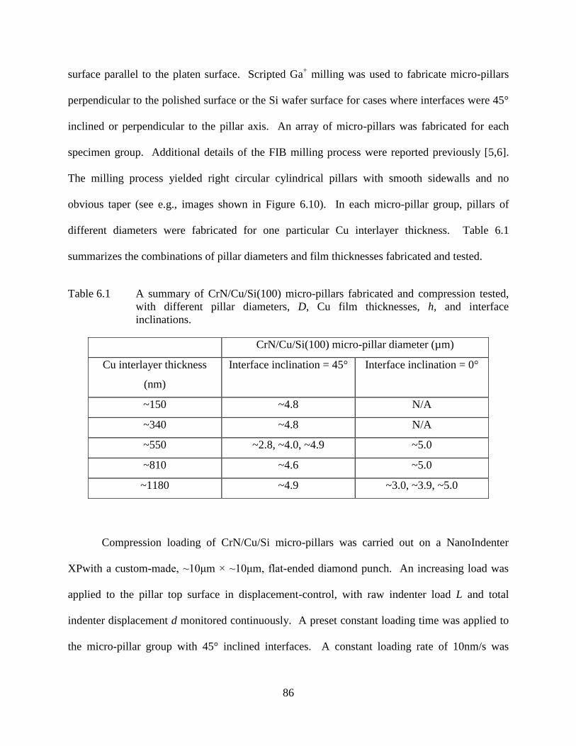
86
surface parallel to the platen surface. Scripted Ga+ milling was used to fabricate micro-pillars
perpendicular to the polished surface or the Si wafer surface for cases where interfaces were 45°
inclined or perpendicular to the pillar axis. An array of micro-pillars was fabricated for each
specimen group. Additional details of the FIB milling process were reported previously [5,6].
The milling process yielded right circular cylindrical pillars with smooth sidewalls and no
obvious taper (see e.g., images shown in Figure 6.10). In each micro-pillar group, pillars of
different diameters were fabricated for one particular Cu interlayer thickness. Table 6.1
summarizes the combinations of pillar diameters and film thicknesses fabricated and tested.
Table 6.1 A summary of CrN/Cu/Si(100) micro-pillars fabricated and compression tested,
with different pillar diameters, D, Cu film thicknesses, h, and interface
inclinations.
CrN/Cu/Si(100) micro-pillar diameter (µm)
Cu interlayer thickness
(nm)
Interface inclination = 45° Interface inclination = 0°
~150 ~4.8 N/A
~340 ~4.8 N/A
~550 ~2.8, ~4.0, ~4.9 ~5.0
~810 ~4.6 ~5.0
~1180 ~4.9 ~3.0, ~3.9, ~5.0
Compression loading of CrN/Cu/Si micro-pillars was carried out on a NanoIndenter
XPwith a custom-made, ~10μm × ~10μm, flat-ended diamond punch. An increasing load was
applied to the pillar top surface in displacement-control, with raw indenter load L and total
indenter displacement d monitored continuously. A preset constant loading time was applied to
the micro-pillar group with 45° inclined interfaces. A constant loading rate of 10nm/s was
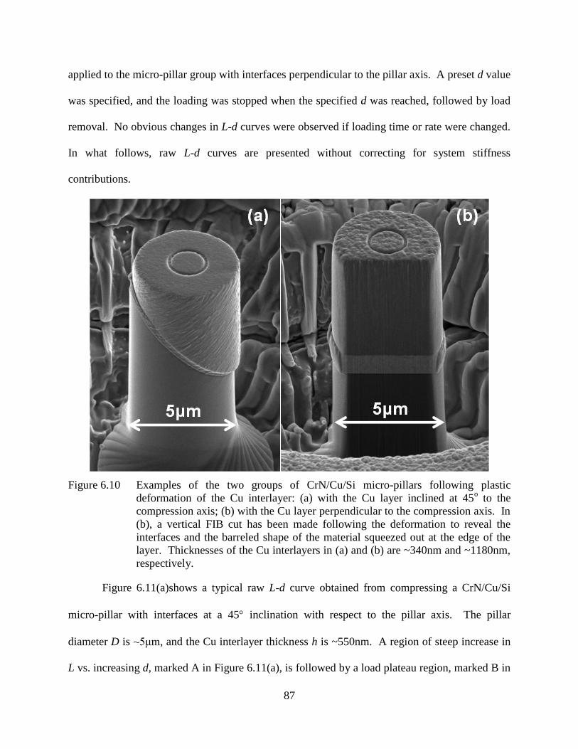
87
applied to the micro-pillar group with interfaces perpendicular to the pillar axis. A preset d value
was specified, and the loading was stopped when the specified d was reached, followed by load
removal. No obvious changes in L-d curves were observed if loading time or rate were changed.
In what follows, raw L-d curves are presented without correcting for system stiffness
contributions.
Figure 6.10 Examples of the two groups of CrN/Cu/Si micro-pillars following plastic
deformation of the Cu interlayer: (a) with the Cu layer inclined at 45o to the
compression axis; (b) with the Cu layer perpendicular to the compression axis. In
(b), a vertical FIB cut has been made following the deformation to reveal the
interfaces and the barreled shape of the material squeezed out at the edge of the
layer. Thicknesses of the Cu interlayers in (a) and (b) are ~340nm and ~1180nm,
respectively.
Figure 6.11(a)shows a typical raw L-d curve obtained from compressing a CrN/Cu/Si
micro-pillar with interfaces at a 45 inclination with respect to the pillar axis. The pillar
diameter D is ~5μm, and the Cu interlayer thickness h is ~550nm. A region of steep increase in
L vs. increasing d, marked A in Figure 6.11(a), is followed by a load plateau region, marked B in

88
Figure 6.11(a), in which d increases at little change in L. As d increases further, an abrupt and
large displacement excursion is observed, marked C in Figure 6.11(a).
Figure 6.11 (a) A typical raw load-displacement curve obtained from compression testing of
one CrN/Cu/Si micro-pillar with 45 inclined interfaces; (b) Raw load-
displacement curves for three pillar diameter, D with Cu thickness h = ~550nm.
Figure 6.12 shows typical morphologies associated with compression of CrN/Cu/Si
micro-pillars with interfaces at a 45 inclination to the axial direction. Figures 6.12(a), 6.12(b),
and 6.12(c) correspond to the three load stages marked A, B, C in Figure 6.11(a). In stages A
and B, no deformation of the CrN and Si sections is observed. Figure 6.12(a) shows that little or
no deformation of the Cu interlayer occurred in the region where L increases sharply with
increasing d. Figure 6.12(b) shows that the load plateau is indeed associated with shear plastic
flow within the Cu interlayer, leading to a small but clear rigid shift of the CrN top pillar portion
with respect to the Si bottom. The load plateau covers a wide range of d values, extending to d >
600nm. Figure 6.12(c) shows that the final abrupt and large displacement excursion, shown in
Figure 6.11, is associated with a catastrophic shear translation of the CrN top pillar portion,
leading to impact of the diamond indenter on the top of Si bottom portion of the pillar. The
sliding marks on the Cu surface, clearly evident in Figure 6.12(c), again offer evidence that
extensive shear plastic flow occurred within the Cu interlayer confined between elastic-brittle
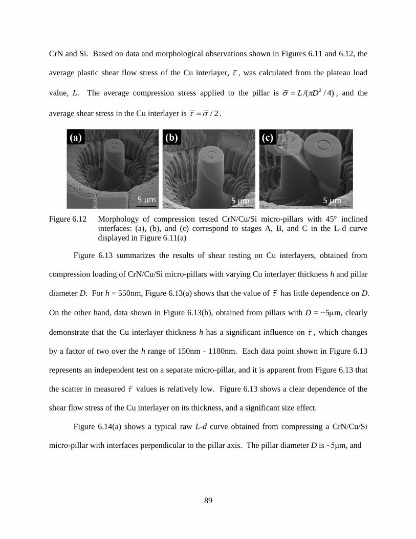
89
CrN and Si. Based on data and morphological observations shown in Figures 6.11 and 6.12, the
average plastic shear flow stress of the Cu interlayer, , was calculated from the plateau load
value, L. The average compression stress applied to the pillar is )4//( 2DL , and the
average shear stress in the Cu interlayer is / 2 .
Figure 6.12 Morphology of compression tested CrN/Cu/Si micro-pillars with 45 inclined
interfaces: (a), (b), and (c) correspond to stages A, B, and C in the L-d curve
displayed in Figure 6.11(a)
Figure 6.13 summarizes the results of shear testing on Cu interlayers, obtained from
compression loading of CrN/Cu/Si micro-pillars with varying Cu interlayer thickness h and pillar
diameter D. For h = 550nm, Figure 6.13(a) shows that the value of has little dependence on D.
On the other hand, data shown in Figure 6.13(b), obtained from pillars with D = ~5m, clearly
demonstrate that the Cu interlayer thickness h has a significant influence on , which changes
by a factor of two over the h range of 150nm - 1180nm. Each data point shown in Figure 6.13
represents an independent test on a separate micro-pillar, and it is apparent from Figure 6.13 that
the scatter in measured values is relatively low. Figure 6.13 shows a clear dependence of the
shear flow stress of the Cu interlayer on its thickness, and a significant size effect.
Figure 6.14(a) shows a typical raw L-d curve obtained from compressing a CrN/Cu/Si
micro-pillar with interfaces perpendicular to the pillar axis. The pillar diameter D is ~5μm, and
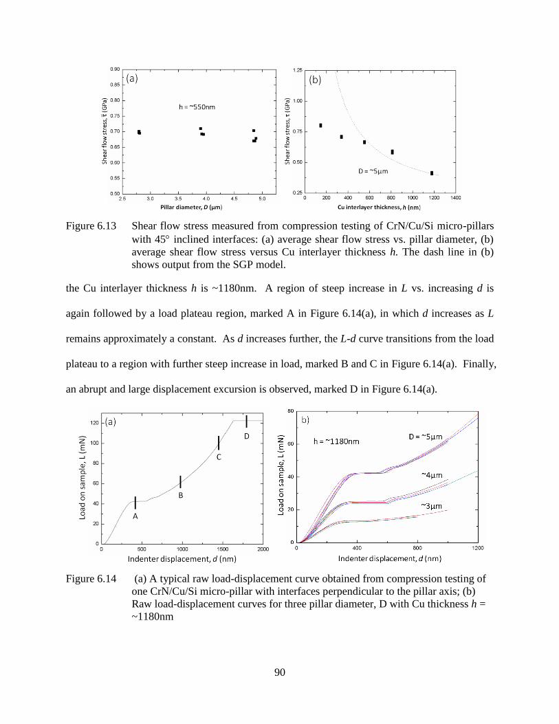
90
Figure 6.13 Shear flow stress measured from compression testing of CrN/Cu/Si micro-pillars
with 45 inclined interfaces: (a) average shear flow stress vs. pillar diameter, (b)
average shear flow stress versus Cu interlayer thickness h. The dash line in (b)
shows output from the SGP model.
the Cu interlayer thickness h is ~1180nm. A region of steep increase in L vs. increasing d is
again followed by a load plateau region, marked A in Figure 6.14(a), in which d increases as L
remains approximately a constant. As d increases further, the L-d curve transitions from the load
plateau to a region with further steep increase in load, marked B and C in Figure 6.14(a). Finally,
an abrupt and large displacement excursion is observed, marked D in Figure 6.14(a).
Figure 6.14 (a) A typical raw load-displacement curve obtained from compression testing of
one CrN/Cu/Si micro-pillar with interfaces perpendicular to the pillar axis; (b)
Raw load-displacement curves for three pillar diameter, D with Cu thickness h =
~1180nm
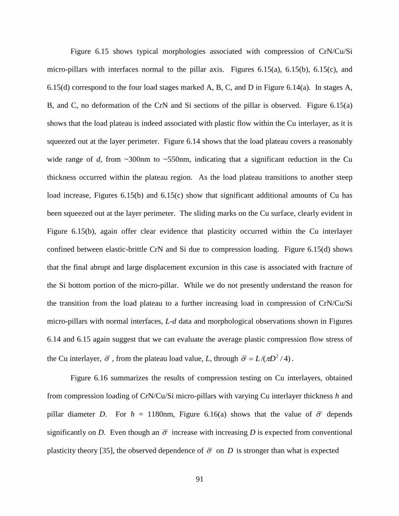
91
Figure 6.15 shows typical morphologies associated with compression of CrN/Cu/Si
micro-pillars with interfaces normal to the pillar axis. Figures 6.15(a), 6.15(b), 6.15(c), and
6.15(d) correspond to the four load stages marked A, B, C, and D in Figure 6.14(a). In stages A,
B, and C, no deformation of the CrN and Si sections of the pillar is observed. Figure 6.15(a)
shows that the load plateau is indeed associated with plastic flow within the Cu interlayer, as it is
squeezed out at the layer perimeter. Figure 6.14 shows that the load plateau covers a reasonably
wide range of d, from ~300nm to ~550nm, indicating that a significant reduction in the Cu
thickness occurred within the plateau region. As the load plateau transitions to another steep
load increase, Figures 6.15(b) and 6.15(c) show that significant additional amounts of Cu has
been squeezed out at the layer perimeter. The sliding marks on the Cu surface, clearly evident in
Figure 6.15(b), again offer clear evidence that plasticity occurred within the Cu interlayer
confined between elastic-brittle CrN and Si due to compression loading. Figure 6.15(d) shows
that the final abrupt and large displacement excursion in this case is associated with fracture of
the Si bottom portion of the micro-pillar. While we do not presently understand the reason for
the transition from the load plateau to a further increasing load in compression of CrN/Cu/Si
micro-pillars with normal interfaces, L-d data and morphological observations shown in Figures
6.14 and 6.15 again suggest that we can evaluate the average plastic compression flow stress of
the Cu interlayer, , from the plateau load value, L, through )4//( 2DL .
Figure 6.16 summarizes the results of compression testing on Cu interlayers, obtained
from compression loading of CrN/Cu/Si micro-pillars with varying Cu interlayer thickness h and
pillar diameter D. For h = 1180nm, Figure 6.16(a) shows that the value of depends
significantly on D. Even though an increase with increasing D is expected from conventional
plasticity theory [35], the observed dependence of on D is stronger than what is expected
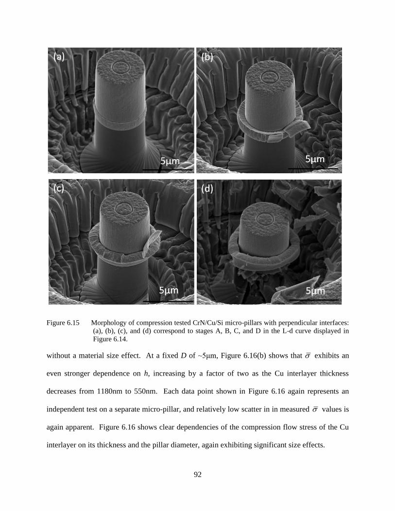
92
Figure 6.15 Morphology of compression tested CrN/Cu/Si micro-pillars with perpendicular interfaces:
(a), (b), (c), and (d) correspond to stages A, B, C, and D in the L-d curve displayed in
Figure 6.14.
without a material size effect. At a fixed D of ~5μm, Figure 6.16(b) shows that exhibits an
even stronger dependence on h, increasing by a factor of two as the Cu interlayer thickness
decreases from 1180nm to 550nm. Each data point shown in Figure 6.16 again represents an
independent test on a separate micro-pillar, and relatively low scatter in in measured values is
again apparent. Figure 6.16 shows clear dependencies of the compression flow stress of the Cu
interlayer on its thickness and the pillar diameter, again exhibiting significant size effects.

93
Figure 6.16 Compression flow stress measured from compression testing of CrN/Cu/Si micro-
pillars with normal interfaces: (a) average compression flow stress vs. D for a Cu
interlayer thickness h of 1180nm, (b) average compression flow stress vs. h at a
fixed pillar diameter D of ~5μm. The dash line shows output from the SGP model.
Through data shown in Figures 6.10 – 6.16, we demonstrated that the micro-pillar
protocol shown in this paper is an effective means for obtaining quantitative measurements on
plasticity of thin metal layers confined between elastic-brittle solids. This protocol further
allows quantitative evaluation of the plastic response of confined thin metal layers in simple yet
significantly different deformation geometries. Furthermore, the measured dependence of flow
stress on Cu film thickness is significantly different depending on whether deformation occurs in
pure shear or normal compression, illustrating that manifestations of mechanical size effects
depend significantly on the deformation geometry in the same material. The present data set,
taken together, offers a good test case for non-local plasticity theories.
6.5 The Material Length Parameter and Trends Predicted by Strain Gradient Plasticity
The purpose of this section is to illustrate that the experimental trends shown in Figures
6.13 and 6.16 are qualitatively captured by predictions of an elementary SGP model with one
consistent set of material parameters. Subsequent efforts will be made to obtain more accurate
agreement with the experimental results. Indeed, in part, the value of the present set of
94
experimental data is that it can serve as a test case for the further development of SGP and
DDP—theories which are not yet sufficiently reliable for applications purposes.
A simple small strain deformation theory of SGP [7,12] will be employed here, which has
three material parameters: a reference flow stress, Y , a strain hardening exponent, N, and a
material length parameter, l. The uniaxial tensile stress-strain relation is assumed to follow the
power law: N
Y . An effective plastic strain is defined as 3/23/2 ,,
2 P
kij
P
kij
P
ij
P
ijP lE ,
which combines the conventional effective plastic strain with an analogous term formed from the
plastic strain gradients and the material length parameter. Elastic strains are neglected, and the
work density under proportional straining is 1)]1/([)( N
PYP ENEU . In the deformation
theory, this work density is identified with the strain energy density of the solid. It reproduces
N
Y in uniaxial tension. The energy in the layer is V
P dVEU )( where V is the layer
volume. At a prescribed average shear strain across the layer in the shear case, or at a prescribed
uniform normal relative displacement of the interfaces in the normal compression case, the
desired strain distribution minimizes among all admissible distributions. Admissibility
requires that the plastic strains vanish at the interfaces with the adjoining segments of the pillar,
modeling the blocked dislocation motion.
The raw L-d curves, shown in Figures 6.11(b) and 6.14(b), indicate that within the flat
plateau region there is relatively little strain hardening. Thus, the predictions which follow will
be based on the limit 0N , such that the solid is rigid-perfectly plastic and characterized by
the tensile yield stress Y and material length parameter l. The computations for the normal
compression case have been carried using a method similar to that detailed in References [12],
but for the present axisymmetric geometry rather than plane strain. Predictions from the model
95
are presented in dimensionless form in Figure 6.17, covering the parameter variations of the
experiments discussed in Section 6.4. The strong dependence on h/l in each part of Figure 6.17
highlights the influence of the material length parameter. The predictions asymptote to those for
a conventional rigid-perfectly plastic solid when h/l > 5. The predicted response of an elastic -
perfectly plastic solid without strain gradient effects, i.e., the limit as / 0l h , is also included
in Figure 6.17 for comparison.
Figure 6.17 Trends predicated by the simple strain gradient plasticity model (solid lines)
described in the text for a solid in the perfectly-plastic limit having a tensile (and
compressive) flow stress and a material length parameter l: For the layer in
confined shear, (a) shows the average shear flow stress normalized by σY versus
the ratio of h to l; For the layer in normal compression, the average compressive
flow stress normalized by σY is shown in (b) versus the ratio of D to h, and in (c)
versus the ratio of h to l. The dashed lines denote model output without strain
gradient effects.
To make a direct comparison with the experimental results shown in Figures 6.13 and
6.16, it is necessary to assign values to Y and l. We have not made independent measurements
of tensile yield stress of Cu thin films, but several papers on this subject exist in the literature
[36]. Reported Y values are in the range of 0.3 to 0.4GPa for Cu thin films of thicknesses
around 1μm or larger. In the following simulations, we take GPaY 35.0 . Then, based on the
SGP results shown in Figure 6.17(a), we choose l to reproduce the experimentally measured
average shear flow stress, GPa70.0 , in Figure 6.13(a) for Cu layers with h=550nm, yielding
an l value of 647nm. It is interesting to note that previous tensile testing of supported Cu thin
96
films [37] and bulge testing of free-standing Cu thin films [38] with surface passivation yielded
respectively l values of ~0.6μm and ~0.35μm, largely consistent with the present fitted l value.
The SGP model predictions, computed with the single parameter set of GPaY 35.0
and l=647nm, are plotted in dimensional form as dashed lines in Figures 6.13(b), 6.16(a), and(b).
As evident from these figures, while the predictions of the simple SGP theory capture the general
trend in each of the three comparisons, they overestimate the strength enhancement for the
thinner layers. In addition, the theory predicts a stronger increase in with pillar diameter than
what is observed in the experimental data. As noted above, the present SGP model is the
simplest theory one could choose. One obvious limitation which is likely to be important is the
fact that the model is isotropic and thereby ignores plastic anisotropy associated with the
dominant <111> fiber texture of the Cu grains. More accurate predictions may require a single
crystal representation of the polycrystalline layer. This and other possibilities are left for the
future. We also note that the present set of polycrystalline Cu interlayers, at any thickness
studied, contain numerous grain boundaries which can serve as dislocation sources. In addition,
all Cu interlayers were deformed to large plastic strains as a result of the loading applied. The
present data should serve as a challenge for both continuum and DDP theories.
6.6 Concluding Remarks
A new experimental protocol has been described for testing plasticity of thin metal films
confined between and bonded to non-deforming, elastic-brittle materials in a micro-pillar
geometry. Experimental results for plastic flow of sputtered Cu thin films in both confined shear
and normal compression have been obtained from CrN/Cu/Si micro-pillars. These results have
been compared to a simple strain gradient plasticity model for a perfectly plastic solid
characterized by an unconstrained tensile yield stress 0.35Y GPa , which was identified using
97
data for free standing films from the literature, and a material length parameter 647nm ,
which was chosen to fit the present shear data for Cu film with a thickness of 550nm . The Cu
film thicknesses tested (550-1180nm ) encompass the material length parameter, and the testing
results reveal a factor of two increase of the effective shear strength of the thinnest film relative
to the thickest film. Furthermore, the effective shear strength of the thickest confined Cu film
(1180nm) is already twice that expected for the Cu shear strength under unconfined conditions,
i.e., 0.4GPa compared with / 3 0.2Y GPa . Thus, the experimental data obtained for the
thinnest Cu films (550nm ) for both the shear test and the normal compression test reveals an
elevation of the effective strength of the Cu by a factor of four above the value expected for
thicker films—a significant size effect. The simple SGP model captures the essential trends of
Cu film deformation in both confined shear and normal compression geometries, but
improvements in quantitative agreement with experimental data will require further modeling
efforts.
Until now, plasticity in metal thin films has been experimentally probed by instrumented
nanoindentation and tensile testing of either free-standing metal films or metal films supported
on polymeric substrates. While substrate effects complicate indentation testing of thin films on
substrates, the experimental complexity associated with tensile testing of free-standing or
supported thin films curtails its wide usage. In comparison, the present experimental results
illustrate that extensive plastic deformation can be induced within thin metal films by using the
micro-pillar protocol described in this letter, and that this protocol allows quantitative plasticity
data to be obtained from the same metal film under significantly different deformation
geometries. The new experimental results presented in this letter offer independent test cases for
confronting new developments in SGP—the wide range of parameters capable of being
98
represented in such data sets is believed to be valuable for further experimental calibration and
validation of non-local plasticity theories.
In addition to the scientific interest in understanding micro- and nano-scale mechanical
behavior of materials, plastic flow in confined thin metal layers is also of significant interest to
surface engineering technologies. Vapor phase deposition of thin ceramic coatings has become
an important means for engineering surfaces of mechanical components [ 39 , 40 ] and
manufacturing tools [41,42]. Satisfactory adhesion of coatings to substrates is critical to the
lifetime of coated systems. To improve adhesion between ceramic coatings and substrates, thin
metallic interlayers are often deposited between the coating and the substrate. When coated
components are subjected to external contact, this adhesion interlayer is put under combinations
of compression and shear. How such thin interlayers deform plastically has a significant bearing
on the mechanical response of the coating/interlayer/substrate system as a whole. Data presented
here represent, to our knowledge, the first set of quantitative data on how thickness and
deformation geometry of thin metal interlayers influence their plastic behavior under stress
conditions relevant to interlayer performance. It is hoped that further investigations along the
lines outlined in this letter will advance the fundamental understanding on how to effectively
engineer coating/substrate interfaces for wide ranging applications of coated mechanical
components and manufacturing tools.
6.7 References
[1] W.C. Oliver, G.M. Pharr, An improved technique for determining hardness and elastic
modulus using load and displacement sensing indentation experiments, Journal of
Materials Research 7, 1564-1583 (1992).
[2] Q. Ma, D.R. Clarke, Size dependent hardness of silver single crystals, J. Mater. Res. 10,
853-863 (1995).
99
[3] T.Y. Tsui, G.M. Pharr, Substrate effects on nanoindentation mechanical property
measurement of soft films on hard substrates, J. Mater. Res. 14, 292-301 (1999).
[4] R. Saha, W.D. Nix, Effects of the substrate on the determination of thin film mechanical
properties by nanoindentation, Acta Mater. 50, 23-38 (2002).
[5] K. Chen, Y. Mu, W.J. Meng, A new experimental approach for evaluating the mechanical
integrity of interfaces between hard coatings and substrates, MRS Comm. 4, 19-23 (2014).
[6] Y. Mu, K. Chen, W. J. Meng, Thickness dependence of flow stress of Cu thin films in
confined shear plastic flow, MRS Comm. 4, 129-133 (2014).
[7] N.A. Fleck, J.W. Hutchinson, Strain gradient plasticity, Adv. Appl. Mech. 33, 295-361
(1997).
[8] J.Y. Shu, N.A. Fleck, E. Van der Giessen, and A. Needleman, Boundary layers in
constrained plastic flow: comparison of nonlocal and discrete dislocation plasticity, J.
Mech. Phys. Solids 49, 1361-1395 (2001).
[9] E. Bittencourt, A. Needleman, M.E. Gurtin, and E. Van der Giessen, A comparison of
nonlocal continuum and discrete dislocation plasticity predictions, J. Mech. Phys. Solids
51(2), 281-310 (2003).
[10] P. Fredriksson and P. Gudmundson, Size-dependent yield strength of thin films, Int. J.
Plasticity 21(9), 1834-1854 (2005).
[11] S.P. Lele and L. Anand, A small-deformation strain-gradient theory for isotropic
viscoplastic materials, Phil. Mag. 88(30-32), 3655-3689 (2008).
[12] C.F. Niordson, J.W. Hutchinson, Basic strain gradient plasticity theories with application
to constrained film deformation, J. Mechanics of Materials and Structures 6, 395-416
(2011).
[13] W.J. Meng, T.J. Curtis, Inductively coupled plasma assisted physical vapor deposition of
titanium nitride coatings, J. Electronic Materials 26, 1297-1302 (1997).
[14] W.J. Meng, T.J. Curtis, L.E. Rehn, and P.M. Baldo, Temperature dependence of
inductively coupled plasma assisted deposition of titanium nitride coatings, Surf. Coat.
Technol. 120/121, 206-212 (1999).
[15] W.J. Meng, E.I. Meletis, L.E. Rehn, P.M. Baldo, Inductively-coupled plasma assisted
deposition and mechanical properties of metal-free and Ti-containing hydrocarbon
coatings, J. Appl. Phys. 87, 2840 (2000).
[16] L.E. Toth, Transition Metal Carbides and Nitrides. Academic Press, New York and
London, 1971.
100
[17] A.J. Perry, J.A. Sue, P.J. Martin, Practical measurement of the residual stress in coatings,
Surf. Coat. Technol. 81, 17 (1996).
[18]. B.D. Cullity, S.R. Stock, Elements of X-ray Diffraction, 3rd
edition, Prentice Hall, New
Jersey (2001).
[19] C. Kral, W. Lengauer, D. Rafaja, P. Ettmayer, Critical review on the elastic properties of
transition metal carbides, nitrides and carbonitrides, Journal of Alloys and Compounds
265, 215–233 (1998).
[20] H.Y. Chen, C.J. Tsai, F.H. Lu, The Young’s modulus of chromium nitride films, Surf.
Coat. Technol. 184, 69–73 (2004).
[21] J.A. Sue, A.J. Perry, J. Vetter, Young’s modulus and stress of CrN deposited by cathodic
vacuum arc evaporation, Surf. Coat. Technol. 68/69, 126-130 (1994).
[22] H. Holleck, Material selection for hard coatings, J. Vac. Sci. Tech. A4, 2661-2669 (1986).
[23] M.E. Straumanis, L.S. Yu, Lattice parameters, densities, expansion coefficients and
perfection of structure of Cu and of Cu-In α phase, Acta Cryst. A25, 676-682 (1969).
[24] K. Chen, W.J. Meng, J.A. Eastman, Interface development in Cu-based structures
transient liquid phase bonded with thin Al foil intermediate layers, Metallurgical and
Materials Transactions A45(9), 3892-3906 (2014).
[25] C. Kittel, Introduction to Solid State Physics, 8th
edition, Wiley (2005).
[26] M.A. Hopcroft, W.D. Nix, T.W. Kenny, What is the Young’s Modulus of Silicon? J.
Microelectromechanical Systems 19, 229-238 (2010).
[27] J.F. Nye, Physical Properties of Crystals: Their Representation by Tensors and Matrices,
Oxford Science Publications, Oxford University Press, New York, 2000.
[28] J.M. Zhang, Y. Zhang, K.W. Xu, V. Ji, Representation surfaces of Young’s modulus and
Poisson’s ratio for bcc transition metals, Physica B 390, 106–111 (2007).
[29] L.J. Vandeperre, F. Giuliani, S.J. Lloyd, W.J. Clegg, The hardness of silicon and
germanium, Acta Materialia 55, 6307–6315 (2007).
[30] W.J. Meng, G.L. Eesley, Growth and mechanical anisotropy of TiN thin films, Thin Solid
Films 271, 108 (1995).
[31] K.H.T. Raman, M.S.R.N. Kiran, U. Ramamurty, G.M. Rao, Structural and mechanical
properties of room temperature sputter deposited CrN coatings, Materials Research
Bulletin 47, 4463–4466 (2012).
101
[32] J. Lin, W.D. Sproul, J.J. Moore, Microstructure and properties of nanostructured thick
CrN coatings, Materials Letters 89, 55–58 (2012).
[33] Z.G. Zhang, O. Rapaud, N. Bonasso, D. Mercs, C. Dong, C. Coddet, Control of
microstructures and properties of dc magnetron sputtering deposited chromium nitride
films, Vacuum 82, 501–509 (2008).
[34] P.H. Mayrhofer, G. Tischler, C. Mitterer, Microstructure and mechanical/thermal
properties of Cr-N coatings deposited by reactive unbalanced magnetron sputtering, Surf.
Coat. Technol. 142_144, 78-84 (2001).
[35] R. Hill, The Mathematical Theory of Plasticity, Oxford University Press, New York
(1998).
[36] H. Huang, F. Spaepen, Tensile testing of free-standing Cu, Ag and Al thin films and
Ag/Cu multilayers, Acta Mater. 48 3261-3269 (2000).
[37] D.Y.W. Yu, F. Spaepen, The yield strength of thin copper films on Kapton, J. Appl. Phys.
95,2991-2997 (2004).
[38] Y. Xiang, J.J. Vlassak, Bauschinger and size effects in thin-film plasticity, Acta Mater.
54, 5449–5460 (2006).
[39] J.C. Jiang, W.J. Meng, A.G. Evans, C.V. Cooper, Structure and mechanics of W-DLC
coated spur gears, Surf. Coat. Technol. 176, 50-56 (2003).
[40] M. Eckels, M.N. Kotzalas, and G.L. Doll, Attaining high levels of bearing performance
with a nanocomposite diamond-like carbon coating, Tribology Transactions 56, 410-416
(2013).
[41] S. PalDey, S.C. Deevi, Single layer and multilayer wear resistant coatings of (Ti,Al)N: a
review, Mater. Sci. Eng. A342, 58-/79 (2003).
[42] D.M. Cao and W.J. Meng, Microscale compression molding of Al with surface
engineered LiGA inserts, Microsyst. Technol. 10, 662-670 (2004).
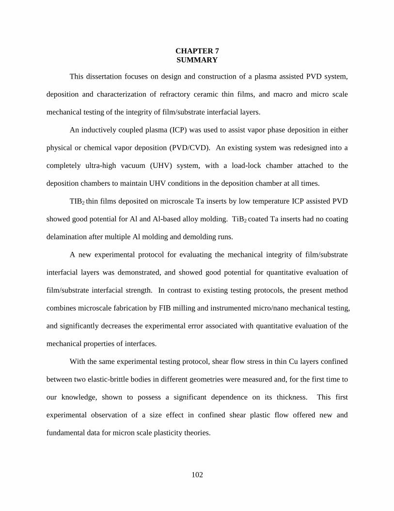
102
CHAPTER 7
SUMMARY
This dissertation focuses on design and construction of a plasma assisted PVD system,
deposition and characterization of refractory ceramic thin films, and macro and micro scale
mechanical testing of the integrity of film/substrate interfacial layers.
An inductively coupled plasma (ICP) was used to assist vapor phase deposition in either
physical or chemical vapor deposition (PVD/CVD). An existing system was redesigned into a
completely ultra-high vacuum (UHV) system, with a load-lock chamber attached to the
deposition chambers to maintain UHV conditions in the deposition chamber at all times.
TIB2 thin films deposited on microscale Ta inserts by low temperature ICP assisted PVD
showed good potential for Al and Al-based alloy molding. TiB2 coated Ta inserts had no coating
delamination after multiple Al molding and demolding runs.
A new experimental protocol for evaluating the mechanical integrity of film/substrate
interfacial layers was demonstrated, and showed good potential for quantitative evaluation of
film/substrate interfacial strength. In contrast to existing testing protocols, the present method
combines microscale fabrication by FIB milling and instrumented micro/nano mechanical testing,
and significantly decreases the experimental error associated with quantitative evaluation of the
mechanical properties of interfaces.
With the same experimental testing protocol, shear flow stress in thin Cu layers confined
between two elastic-brittle bodies in different geometries were measured and, for the first time to
our knowledge, shown to possess a significant dependence on its thickness. This first
experimental observation of a size effect in confined shear plastic flow offered new and
fundamental data for micron scale plasticity theories.
103
APPENDIX. LETTERS OF COPYRIGHT PERMISSION
1. Permission of Using Published Material from Microsystem Technologies
Springer, Permissions <[email protected]>
Jun 19
to me
Dear Yang Mu,
Please see enclosed permission letter attached. Sincerely,
Rights and Permissions
Springer Science+Business Media
Tiergartenstr. 17
69121 Heidelberg
Germany
From: Yang Mu [mailto:[email protected]]
Sent: Friday, June 19, 2015 12:21 AM
To: Onlineservice, SCSC
Subject: permission request
To Whom it May Concern,
This is Yang Mu, a Ph. D candidate from Louisiana State University Department of Mechanical
Engineering, and also the first author of the following paper published in Microsystem
technology.
“Low temperature deposited titanium boride thin films and their application to surface
engineering of microscale mold inserts”, Microsystem Technology, Volume 18, Pages 667-677
(2012)
104
I am finishing up my PhD dissertation and would like to include the work described above into
the dissertation. I would like to confirm with you that this use is within the copyright retained
for authors. Thank you very much for your time and help.
--
Yang Mu, Graduate Student
2420, Patrick F. Taylor Hall
Mechanical Engineering Department
Louisiana State University
Baton Rouge, Louisiana 70803, USA
225-578-5947 (office)
225-578-9195 (fax)
2. Permission of Using Published Material from Extreme Mechanics Letters
This is a License Agreement between Yang Mu ("You") and Elsevier ("Elsevier")
providedby Copyright Clearance Center ("CCC"). The license consists of your
order details, the terms and conditions provided by Elsevier, and the payment
terms and conditions.
Supplier Elsevier Limited
The Boulevard,Langford Lane
Kidlington,Oxford,OX5 1GB,UK
Registered Company Number 1982084
Customer name Yang Mu
Customer address Louisiana State University
BATON ROUGE, LA 70803
License number 3663370763479
License date Jul 06, 2015
Licensed content publisher Elsevier
Licensed content publication Extreme Mechanics Letters
Licensed content title Micropillar measurements of plasticity in confined Cu thin
films
Licensed content author Yang Mu,J.W. Hutchinson,W.J. Meng
Licensed content date December 2014
105
VITA
Yang Mu was born in 1984, in Hubei Province, People’s Republic of China. He
studied in Materials Science and Engineering department in Beijing Institute of
Technology, China, from 2002 to 2006, and obtained Bachelor’s degree in Materials
Science and Engineering. He became a graduate student in Louisiana State University in
Mechanical Engineering department started at 2007. Currently, he is a philosophy of
doctorial candidate major in Mechanical Engineering. His research interest is focused on
vacuum technology, thin films preparation and characterization, and micro/nano scale
mechanical response of materials.