deposition of thin films has been of interest for almost ... · 23-1 thin films: an introduction...
TRANSCRIPT

23-1
Thin Films: An Introduction
Deposition of thin films has been of interest for almost 100 years
examples solar panels
oxide thin filmon a substrate

•optical thin films (Filters, Anti-reflection, Cosmetic, security devices, architectural)
•surface chemical modification(hydrophobic, bio & chemical sensors)
•barrier coatings (packaging films, ultra-barriers)
•electrical coatings (anti-static, shielding, displays)
•hard and wear resistant coatings (cutting tools, bearings, engine parts, plastic optics)
•decorative coatings (watch cases, bathroom furniture, door furniture, plastic mouldings, metallic yarns)
Many Applications
23-2

23-3
Film Growth Methods
can be divided into two groups
1. Vapour Phase Growth 2. Liquid Phase Growth
evaporation, MBECVD, ALD (atomic laser desorption)sputtering.....
electrochemicalCSD (chemical solution deposition)Langmuir-Blodgett FilmsSelf-assembled monolayers (SAMs)and more.......

Comparison of thin film deposition methods
•Difficult to scale •Often uses hazardous liquids or gases
•Gives good control of coating chemistry
CVD
•high voltages •Fast •Wide range of inorganic materials
e-Beam Evaporation
•Limited range of materials •Low density films without ion or plasma assist
•Fast •Relatively simple
Thermal Evaporation
•relatively slow
•Dense films •Good uniformity •Wide range of inorganic materials
Sputtering
Disadvantages Advantages Technique
23-4

23-5
Fundamentals of Film Growth
Nucleation
Thin films almost never grow as perfect slabs.It is important to consider the way in which a film can grow as "patches"which eventually coalesce to form a complete coherent layer.
Three major mechanisms
1. Island or Wolmer-Weber Growth2. Layer or Frank -Van der Merwe Growth3. Island -layer of Stranski -Krastonov Growth
let's look at these

23-6
Cross-section views of the three primary modes of thin film growth including (a) Volmer-Weber (VW: island formation), (b) Frank-van der Merwe (FM: layer-by-layer), and (c) Stranski-Krastanov (SK: layer-plus-island). Each mode is shown for several different amounts of surface coverage, Θ.

In Volmer-Weber (VW) growth, adatom-adatom interactions are stronger than those of the adatom with the surface, leading to the formation of three-dimensional adatomclusters or islands. -metals grown on insulators such as MgO do this.
during Frank-van der Merwe (FM) growth, adatoms attach preferentially to surface sites resulting in atomically smooth, fully formed layers. This layer-by-layer growth is two dimensional, indicating that complete films form prior to growth of subsequent layers
Stranski-Krastanov growth is an intermediary process characterized by both 2D layer and 3D island growth. Transition from the layer-by-layer to island-based growth occurs at a critical layer thickness which is highly dependent on the chemical and physical properties, such as surface energies and lattice parameters, of the substrate and film.[
Summary
23-7Islands can mean Islands can mean Islands can mean Islands can mean nanostructrenanostructrenanostructrenanostructre growthgrowthgrowthgrowth

23-8
Important to note that SK and VW growth change from2D to 3D at a critical thickness.
Examples
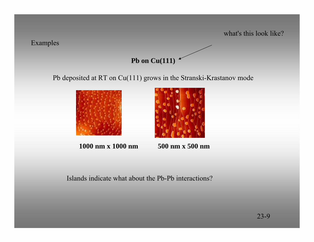
Pb on Cu(111)
Pb deposited at RT on Cu(111) grows in the Stranski-Krastanov mode
1000 nm x 1000 nm 500 nm x 500 nm
Islands indicate what about the Pb-Pb interactions?
23-9
what's this look like?

Palladium Nanocrystals on Aluminium Oxide (Al2O3):
film grows according to the Volmer-Weber mode; atoms nucleate in individual 3D clusters.
atomic resolution of Pd nanoclusters(STM)
what plane is it?
23-10
23-11
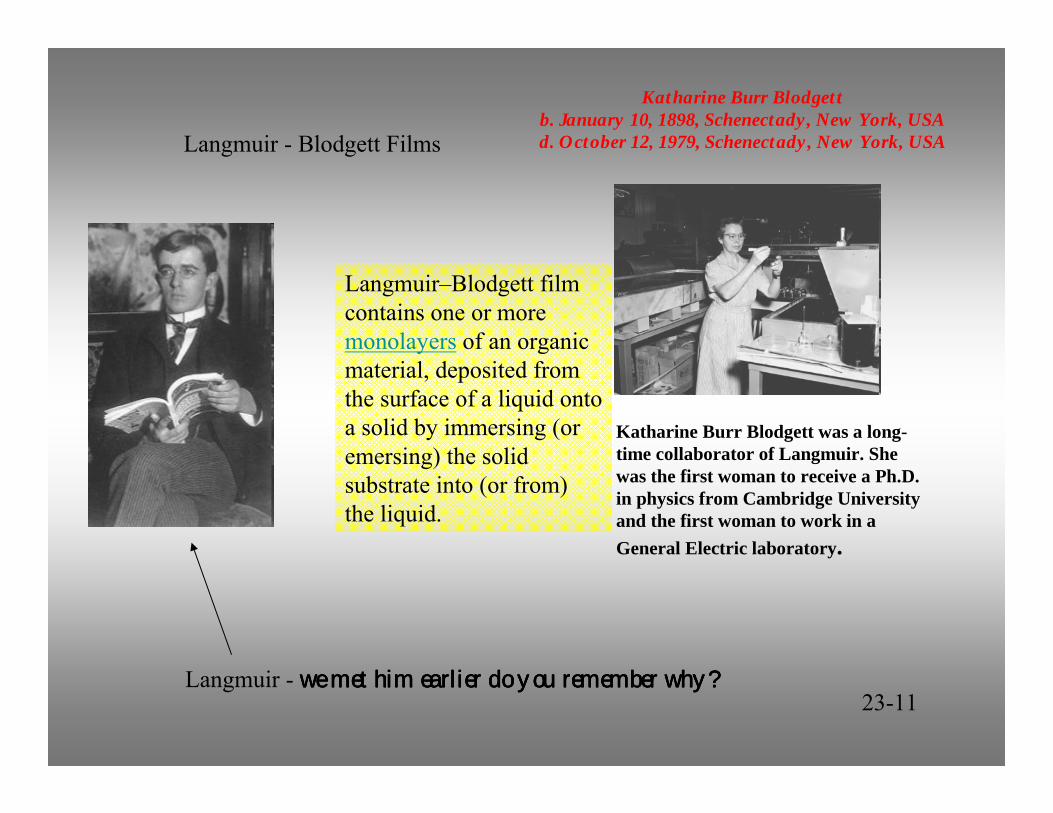
Langmuir - Blodgett Films
Katharine Burr Blodgett was a long-time collaborator of Langmuir. She was the first woman to receive a Ph.D. in physics from Cambridge University and the first woman to work in a General Electric laboratory.
Katharine Burr Blodgettb. January 10, 1898, Schenectady, New York, USA d. October 12, 1979, Schenectady, New York, USA
Langmuir - we met him earlier do you remember why?we met him earlier do you remember why?we met him earlier do you remember why?we met him earlier do you remember why?
Langmuir�Blodgett film contains one or more monolayers of an organic material, deposited from the surface of a liquid onto a solid by immersing (or emersing) the solid substrate into (or from) the liquid.

23-12
Layers of Amphphilic molecules transferred from the liquid gas interface (commonly water-air) onto solid.
Amphiphile: molecule that is insoluble in water with one endhydrophobic and one end hydrophilic

23-13
Classic Example of an amphiphile is stearic acid
also called surfactants
solubility in water depends on balance between alkyl chain length and the strength of hydrophilic head
if hydrophobic head is too weak then no LB film
if too strong molecule stays in solution phase --no LB film
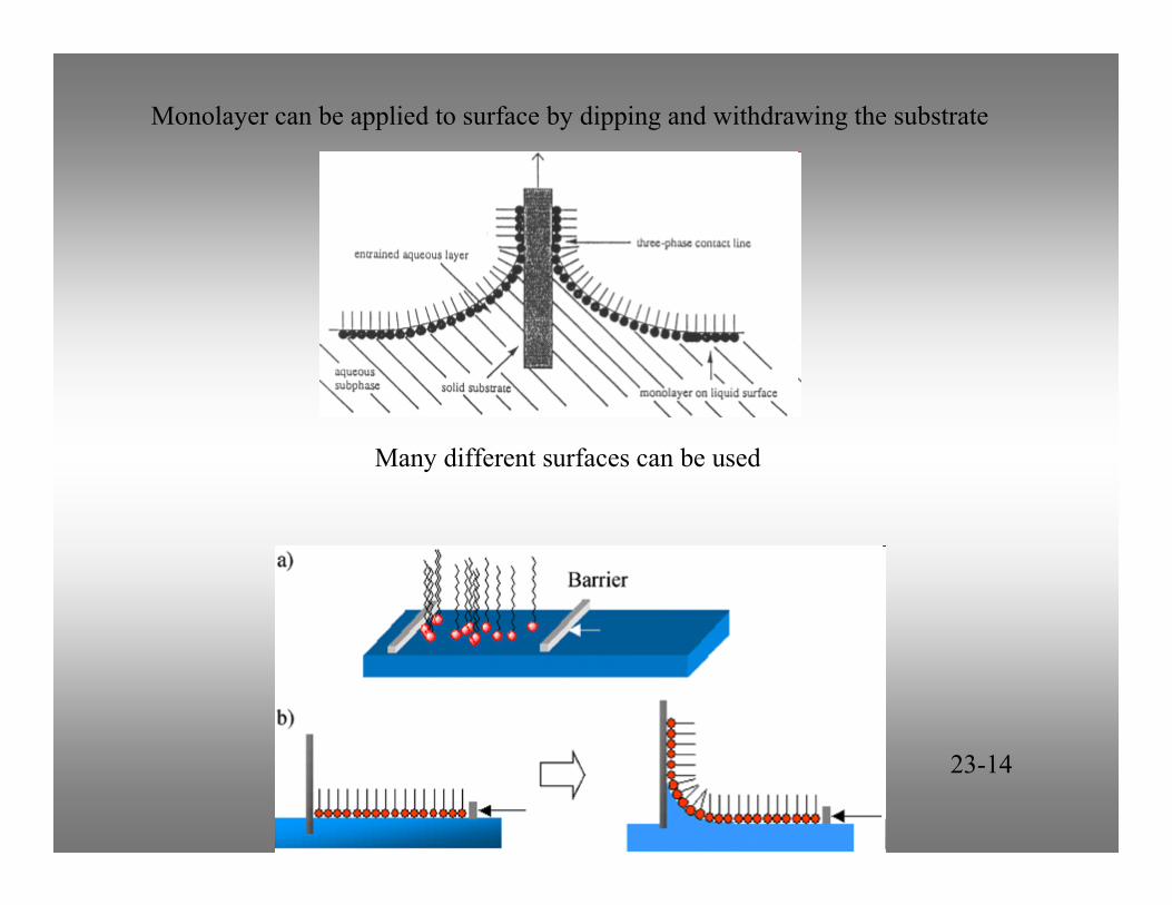
Monolayer can be applied to surface by dipping and withdrawing the substrate
Many different surfaces can be used
23-14
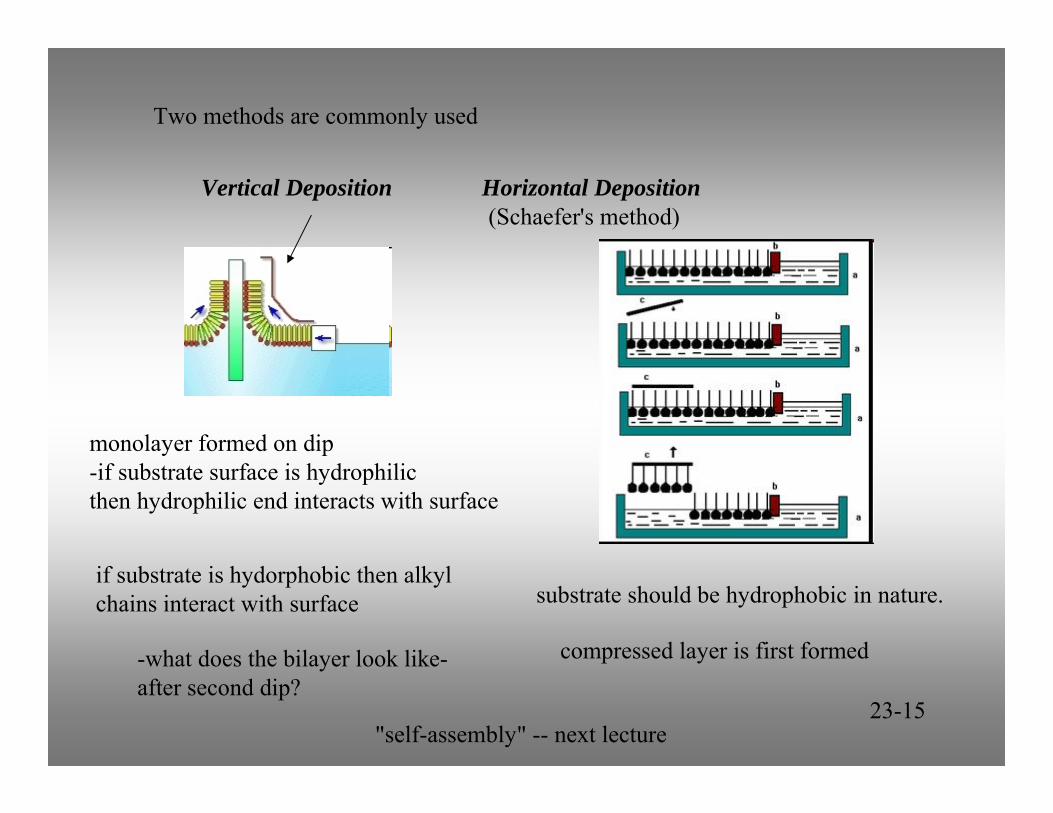
Two methods are commonly used
23-15
Vertical Deposition Horizontal Deposition(Schaefer's method)
substrate should be hydrophobic in nature.
compressed layer is first formed
monolayer formed on dip-if substrate surface is hydrophilicthen hydrophilic end interacts with surface
if substrate is hydorphobic then alkylchains interact with surface
-what does the bilayer look like-after second dip?
"self-assembly" -- next lecture
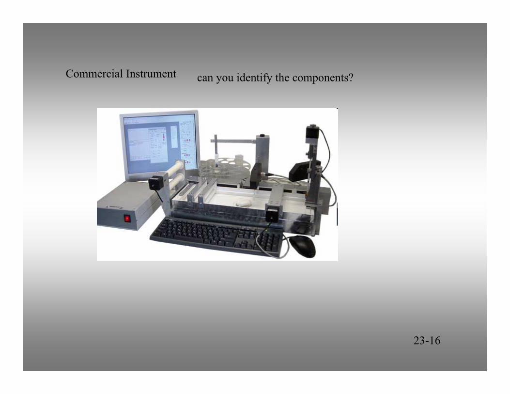
Commercial Instrument can you identify the components?
23-16

LB films --examples
23-17
organic nano-stepsAmphiphilic fullerenes deposited at the air-water interface on a Langmuir trough. After compression, successive transfers were carried out on a standard surf to obtain steps. The step height is about 6.0 nm.
Lipid film deposited by Langmuir-Blodgett technique on mica. Scanned at 100 microns AFM in Tapping Mode in water at room temperature.