dept. of computer and information science (ida) linköpings
TRANSCRIPT
Dept. of Computer and Information Science (IDA)
Linköpings universitet
Sweden
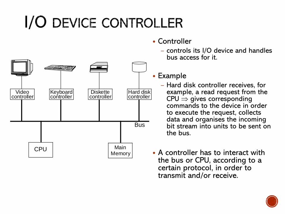
MainMemory
CPU
Video controller
Bus
Keyboardcontroller
Diskettecontroller
Hard diskcontroller
• Controller– controls its I/O device and handles
bus access for it.
• Example– Hard disk controller receives, for
example, a read request from the CPU gives corresponding commands to the device in order to execute the request, collects data and organises the incoming bit stream into units to be sent on the bus.
• A controller has to interact with the bus or CPU, according to a certain protocol, in order to transmit and/or receive.
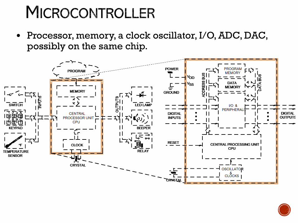
• Processor, memory, a clock oscillator, I/O, ADC, DAC, possibly on the same chip.
• For embedded control applications– Reading sensors, setting actuators
– Mostly dealing with events (bits): data is present, but not in huge amounts
– e.g., automotive control systems, wearable health-care devices, pacemaker, disk drive, digital camera, washing machine, microwave oven
• Microcontroller features– On-chip peripherals
• Timers, analog-digital converters, serial communication, etc.
• Tightly integrated for programmer, typically part of register space
– On-chip program and data memory
– Direct programmer access to many of the chip’s pins
– Specialized instructions for bit-manipulation and other low-level operations

• Processor has one or more N-bit ports
• Processor’s software reads and writes a port
just like a register
– E.g., PA = 0xF2; x=PA.2;
CPU
PA0..PA7
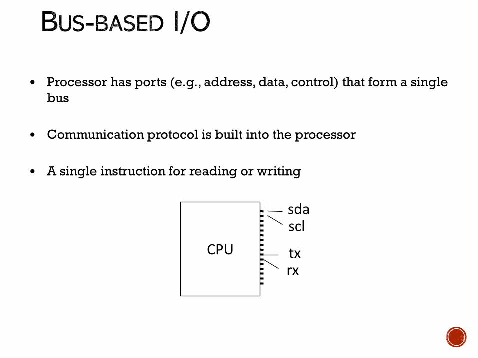
• Processor has ports (e.g., address, data, control) that form a single
bus
• Communication protocol is built into the processor
• A single instruction for reading or writing
CPU
sdascl
txrx
embedded
device1
00 1
1 0 11
Sending UART
1 0 0 1 1 0 1 1
Receiving UART
1 0 0 1 1 0 1 1
start bitdata
end bit
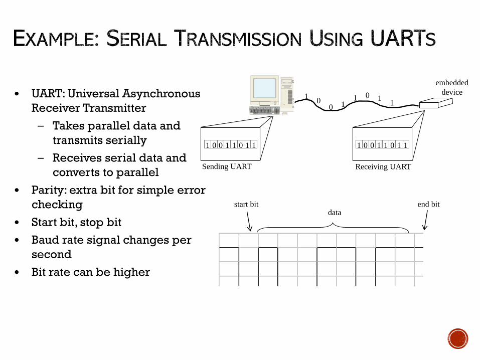
• UART: Universal Asynchronous
Receiver Transmitter
– Takes parallel data and
transmits serially
– Receives serial data and
converts to parallel
• Parity: extra bit for simple error
checking
• Start bit, stop bit
• Baud rate signal changes per
second
• Bit rate can be higher

• Transmitter
– Host process writes in the transmit buffer of UART
– Sends “start bit” over transmit pin (tx): Signals beginning of transmission to the
remote UART
– Shifts out the data in the buffer over tx on a specified rate
– Transmits (optional) parity bit
– Signals host processor indicating that is ready to transmit more
embedded
device1
00 1
1 0 11
Sending UART
1 0 0 1 1 0 1 1
Receiving UART
1 0 0 1 1 0 1 1
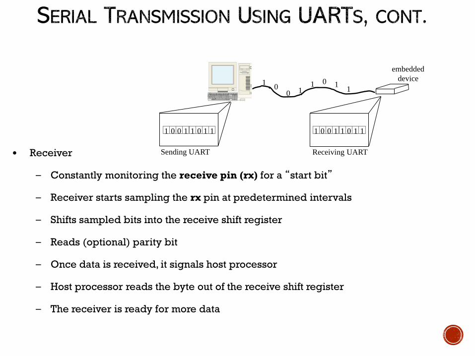
• Receiver
– Constantly monitoring the receive pin (rx) for a “start bit”
– Receiver starts sampling the rx pin at predetermined intervals
– Shifts sampled bits into the receive shift register
– Reads (optional) parity bit
– Once data is received, it signals host processor
– Host processor reads the byte out of the receive shift register
– The receiver is ready for more data
embedded
device1
00 1
1 0 11
Sending UART
1 0 0 1 1 0 1 1
Receiving UART
1 0 0 1 1 0 1 1

11
D
C
ST
ART
A6
A5
A0
R/w
ACK
D8
D7
D0
ACK
ST
OP
From Servant
From receiver
Typical read/write cycle
SDA
SCL
SDA
SCL
SDA
SCL
SDA
SCL
Start condition Sending 0 Sending 1 Stop condition
SCLSDA
Micro-controller(master)
EEPROM(servant)
Temp. Sensor(servant)
LCD-controller(servant)
< 400 pF
Addr=0x01 Addr=0x02 Addr=0x03

• When processor only supports bus-based I/O but parallel I/O needed
• Each port on peripheral connected to a register within peripheral that is read/written by the processor
Processor Memory
Parallel I/O peripheral
Port A
System bus
Port CPort B
Adding parallel I/O to a bus-based I/O processor

• When processor supports port-based I/O but more ports needed
• One or more processor ports interface with parallel I/O peripheral extending total number of ports available for I/O
– e.g., extending 4 ports to 6 ports in figure
Processor
Parallel I/O peripheral
Port A Port B Port C
Port 0
Port 1
Port 2
Port 3
Extended parallel I/O

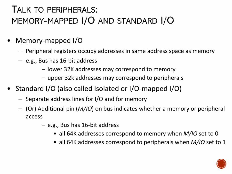
• Memory-mapped I/O
– Peripheral registers occupy addresses in same address space as memory
– e.g., Bus has 16-bit address
– lower 32K addresses may correspond to memory
– upper 32k addresses may correspond to peripherals
• Standard I/O (also called Isolated or I/O-mapped I/O)
– Separate address lines for I/O and for memory
– (Or) Additional pin (M/IO) on bus indicates whether a memory or peripheral access
– e.g., Bus has 16-bit address
• all 64K addresses correspond to memory when M/IO set to 0
• all 64K addresses correspond to peripherals when M/IO set to 1

▪Memory-mapped I/O
• No special instructions
• Assembly instructions involving memory like MOV and ADD work with peripherals as well
▪Standard I/O
No loss of memory addresses to peripherals
Simpler address decoding logic in peripherals
Small number of devices -> high-order address bits can be ignored (smaller and/or faster comparators)
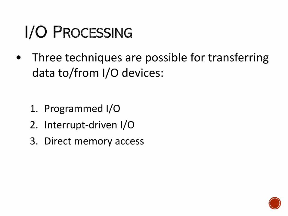
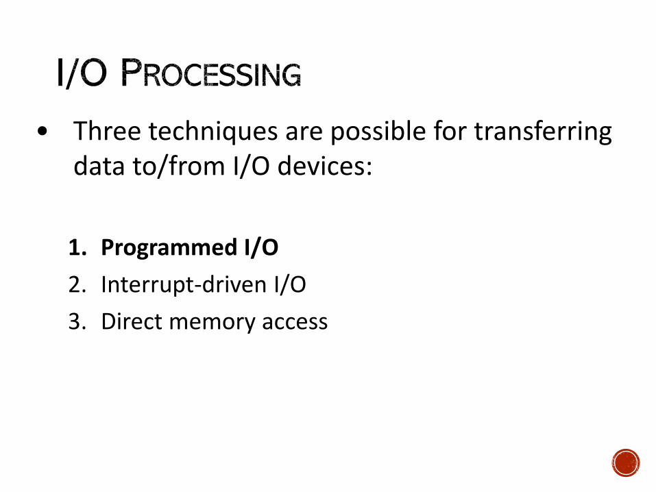
• Three techniques are possible for transferring data to/from I/O devices:
1. Programmed I/O
2. Interrupt-driven I/O
3. Direct memory access
• Three techniques are possible for transferring data to/from I/O devices:
1. Programmed I/O
2. Interrupt-driven I/O
3. Direct memory access

• The CPU executes a sequence of instructions, being in direct control of the I/O operations (sensing device status, read/write commands, etc.). When the CPU issues a command to the I/O module, it must wait until the I/O operation is complete.
• A lot of wasted time, because the CPU is much faster then devices.
1. Programmed I/O
2. Interrupt-driven I/O
3. Direct memory access
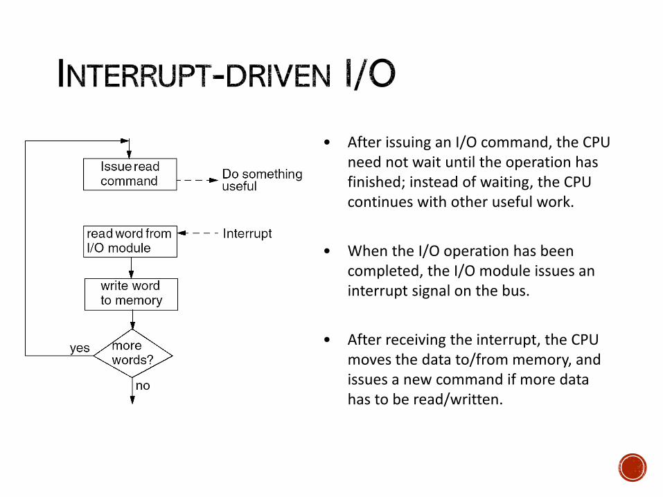
• After issuing an I/O command, the CPU need not wait until the operation has finished; instead of waiting, the CPU continues with other useful work.
• When the I/O operation has been completed, the I/O module issues an interrupt signal on the bus.
• After receiving the interrupt, the CPU moves the data to/from memory, and issues a new command if more data has to be read/written.

• Interrupt– Asynchronous electrical signal from a peripheral to the processor
• Consists of:– Interrupt pin (on the outside of the processor chip)
• If Int is 1, processor suspends current program, jumps to an Interrupt Service Routine, or ISR
– Interrupt service routine (ISR)• Small piece of software executed by the processor when an interrupt is
asserted
• Programmer must write and “install” the ISR
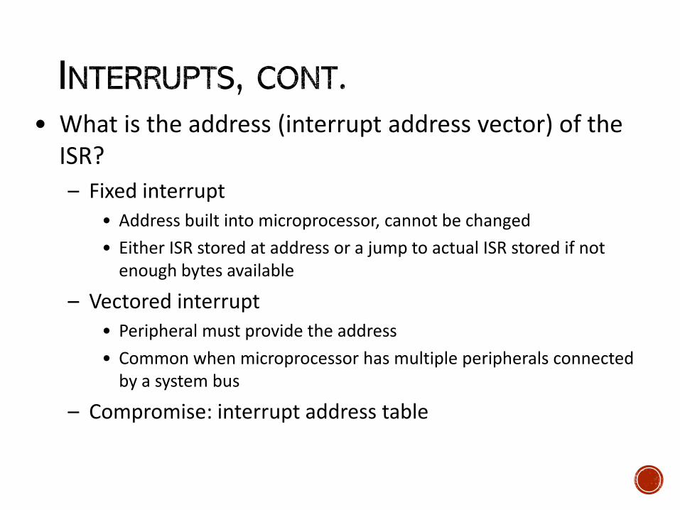
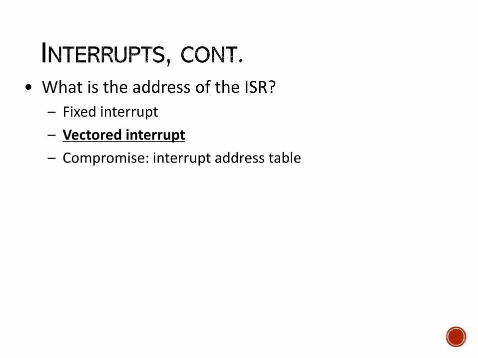
• What is the address (interrupt address vector) of the ISR?
– Fixed interrupt
• Address built into microprocessor, cannot be changed
• Either ISR stored at address or a jump to actual ISR stored if not enough bytes available
– Vectored interrupt• Peripheral must provide the address
• Common when microprocessor has multiple peripherals connected by a system bus
– Compromise: interrupt address table

• What is the address of the ISR?
– Fixed interrupt
– Vectored interrupt
– Compromise: interrupt address table
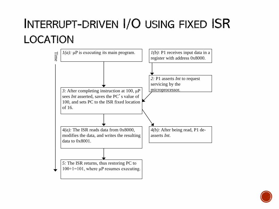
1(a): μP is executing its main program. 1(b): P1 receives input data in a
register with address 0x8000.
2: P1 asserts Int to request
servicing by the
microprocessor.3: After completing instruction at 100, μP
sees Int asserted, saves the PC’s value of
100, and sets PC to the ISR fixed location
of 16.
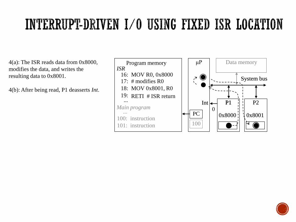
4(a): The ISR reads data from 0x8000,
modifies the data, and writes the resulting
data to 0x8001.
5: The ISR returns, thus restoring PC to
100+1=101, where μP resumes executing.
4(b): After being read, P1 de-
asserts Int.
Tim
e
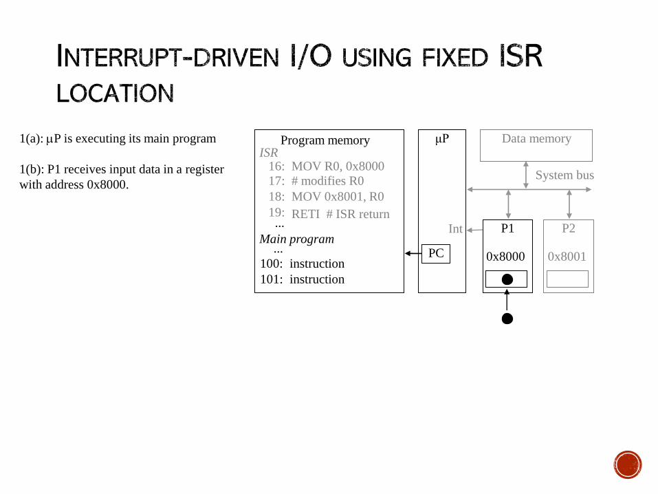
1(a): P is executing its main program
1(b): P1 receives input data in a register
with address 0x8000.
μP
P1 P2
System bus
Int
Data memory
0x8000 0x8001
16: MOV R0, 0x8000
17: # modifies R0
18: MOV 0x8001, R0
19: RETI # ISR return
ISR
100:
101:
instruction
instruction
...
Main program...
Program memory
PC
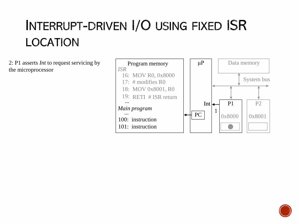
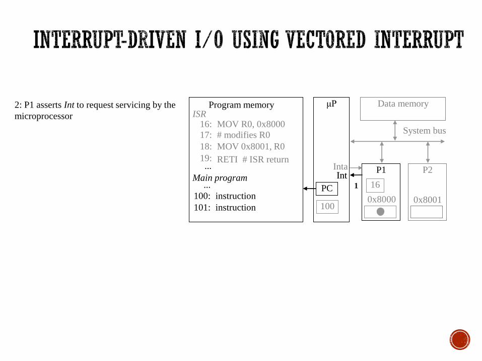
2: P1 asserts Int to request servicing by
the microprocessor
μP
P1 P2
System bus
Data memory
0x8000 0x8001
16: MOV R0, 0x8000
17: # modifies R0
18: MOV 0x8001, R0
19: RETI # ISR return
ISR
100:
101:
instruction
instruction
...
Main program...
Program memory
PC
IntInt
1
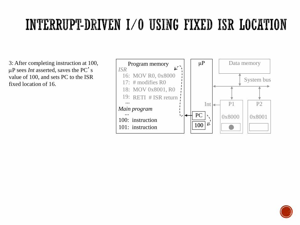
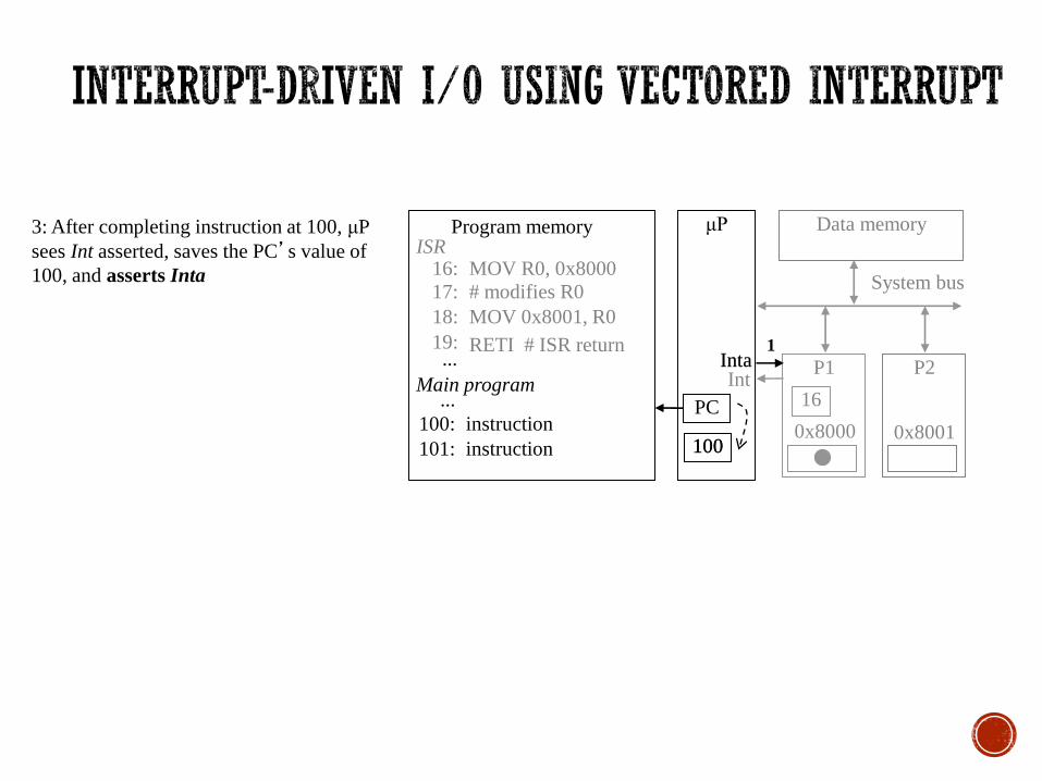
3: After completing instruction at 100,
P sees Int asserted, saves the PC’s
value of 100, and sets PC to the ISR
fixed location of 16.
μP
P1 P2
System bus
Data memory
0x8000 0x8001
16: MOV R0, 0x8000
17: # modifies R0
18: MOV 0x8001, R0
19: RETI # ISR return
ISR
100:
101:
instruction
instruction
...
Main program...
Program memory
PC
Int
100100
μP
P1 P2
System bus
Data memory
0x8000 0x8001
16: MOV R0, 0x8000
17: # modifies R0
18: MOV 0x8001, R0
19: RETI # ISR return
ISR
100:
101:
instruction
instruction
...
Main program...
Program memory
PC
Int
4(a): The ISR reads data from 0x8000,
modifies the data, and writes the
resulting data to 0x8001.
4(b): After being read, P1 deasserts Int.
100
Int0
P1
System bus
P1
0x8000
P2
0x8001

5: The ISR returns, thus restoring PC to
100+1=101, where P resumes
executing.
μP
P1 P2
System bus
Data memory
0x8000 0x8001
16: MOV R0, 0x8000
17: # modifies R0
18: MOV 0x8001, R0
19: RETI # ISR return
ISR
100:
101:
instruction
instruction
...
Main program...
Program memory
PC
Int
100100+1
16: MOV R0, 0x8000
17: # modifies R0
18: MOV 0x8001, R0
19: RETI # ISR return
ISR
100:
101:
instruction
instruction
...
Main program...
100
• What is the address of the ISR?
– Fixed interrupt
– Vectored interrupt
– Compromise: interrupt address table

1(a): μP is executing its main program. 1(b): P1 receives input data in a
register with address 0x8000.
2: P1 asserts Int to request servicing
by the microprocessor.3: After completing instruction at 100, μP sees Int
asserted, saves the PC’s value of 100, and asserts
Inta.
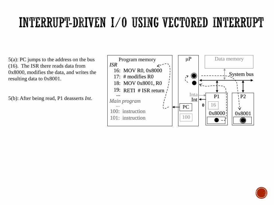
5(a): μP jumps to the address on the bus (16).
The ISR there reads data from 0x8000, modifies
the data, and writes the resulting data to 0x8001.
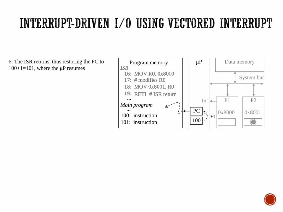
6: The ISR returns, thus restoring PC to
100+1=101, where μP resumes executing.
5(b): After being read, P1 deasserts
Int.
Tim
e
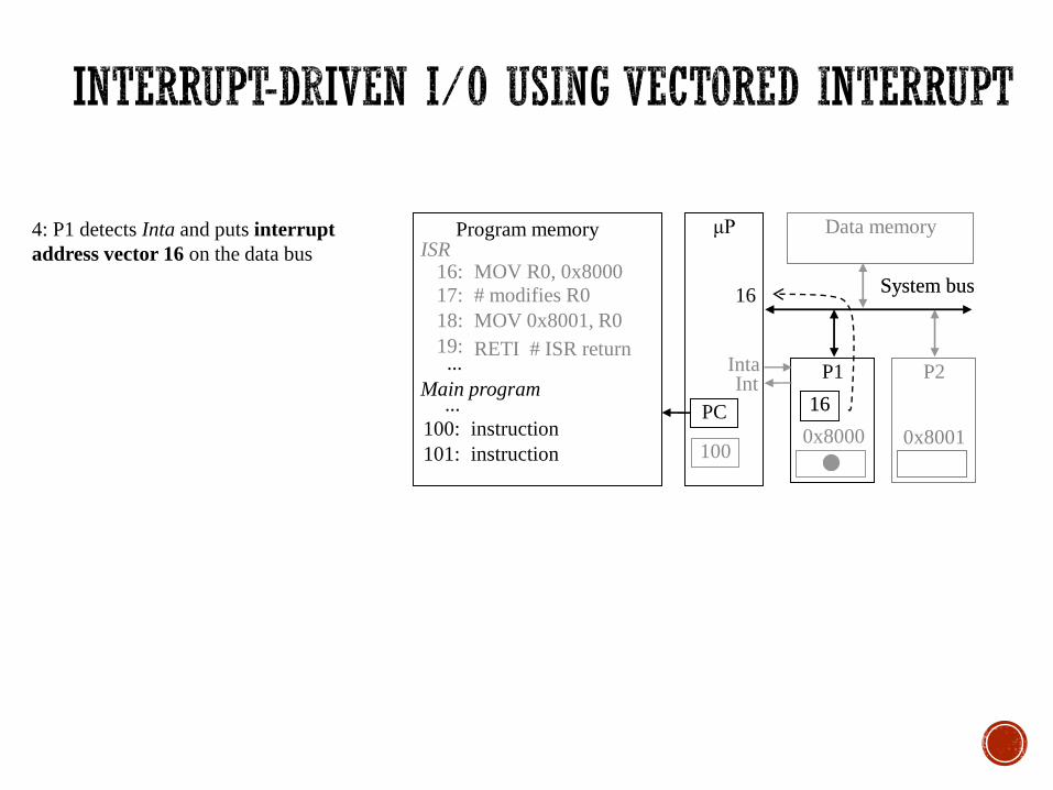
4: P1 detects Inta and puts interrupt
address vector 16 on the data bus.

μP
P1 P2
System bus
Data memory
0x8000 0x8001
16: MOV R0, 0x8000
17: # modifies R0
18: MOV 0x8001, R0
19: RETI # ISR return
ISR
100:
101:
instruction
instruction
...
Main program...
Program memory
PC
100
IntInta
16
1(a): P is executing its main program
1(b): P1 receives input data in a register
with address 0x8000.
μP
P1 P2
System bus
Data memory
0x8000 0x8001
16: MOV R0, 0x8000
17: # modifies R0
18: MOV 0x8001, R0
19: RETI # ISR return
ISR
100:
101:
instruction
instruction
...
Main program...
Program memory
PC
100
Inta
16
2: P1 asserts Int to request servicing by the
microprocessor
Int1
Int
3: After completing instruction at 100, μP
sees Int asserted, saves the PC’s value of
100, and asserts Inta
μP
P1 P2
System bus
Data memory
0x8000 0x8001
16: MOV R0, 0x8000
17: # modifies R0
18: MOV 0x8001, R0
19: RETI # ISR return
ISR
100:
101:
instruction
instruction
...
Main program...
Program memory
PC
IntInta
16
100100
1Inta
μP
P1 P2
System bus
Data memory
0x8000 0x8001
16: MOV R0, 0x8000
17: # modifies R0
18: MOV 0x8001, R0
19: RETI # ISR return
ISR
100:
101:
instruction
instruction
...
Main program...
Program memory
PC
IntInta
16
100
4: P1 detects Inta and puts interrupt
address vector 16 on the data bus
16
16
System bus
5(a): PC jumps to the address on the bus
(16). The ISR there reads data from
0x8000, modifies the data, and writes the
resulting data to 0x8001.
5(b): After being read, P1 deasserts Int.
μP
P1 P2
System bus
Data memory
0x8000 0x8001
16: MOV R0, 0x8000
17: # modifies R0
18: MOV 0x8001, R0
19: RETI # ISR return
ISR
100:
101:
instruction
instruction
...
Main program...
Program memory
PC
IntInta
16
100
16: MOV R0, 0x8000
17: # modifies R0
18: MOV 0x8001, R0
19: RETI # ISR return
ISR
100:
101:
instruction
instruction
...
Main program...
P1 P2
0x8000 0x8001
System bus
0
Int
6: The ISR returns, thus restoring the PC to
100+1=101, where the μP resumes
μP
P1 P2
System bus
Data memory
0x8000 0x8001
16: MOV R0, 0x8000
17: # modifies R0
18: MOV 0x8001, R0
19: RETI # ISR return
ISR
100:
101:
instruction
instruction
...
Main program...
Program memory
PC
Int
100100+1
16: MOV R0, 0x8000
17: # modifies R0
18: MOV 0x8001, R0
19: RETI # ISR return
ISR
100:
101:
instruction
instruction
...
Main program...
100

• What is the address of the ISR?
– Fixed interrupt
– Vectored interrupt
– Compromise: interrupt address table
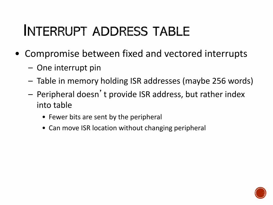
• Compromise between fixed and vectored interrupts
– One interrupt pin
– Table in memory holding ISR addresses (maybe 256 words)
– Peripheral doesn’t provide ISR address, but rather index into table
• Fewer bits are sent by the peripheral
• Can move ISR location without changing peripheral
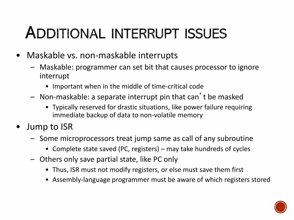
• Maskable vs. non-maskable interrupts– Maskable: programmer can set bit that causes processor to ignore
interrupt• Important when in the middle of time-critical code
– Non-maskable: a separate interrupt pin that can’t be masked• Typically reserved for drastic situations, like power failure requiring
immediate backup of data to non-volatile memory
• Jump to ISR– Some microprocessors treat jump same as call of any subroutine
• Complete state saved (PC, registers) – may take hundreds of cycles
– Others only save partial state, like PC only• Thus, ISR must not modify registers, or else must save them first
• Assembly-language programmer must be aware of which registers stored

• Advantage over programmed I/O
– Instead of waiting the operation to be finished, the CPU can do some useful work
• Still a problem
– The CPU has to take care of each data unit (word), to move it to/from memory, and to issue an I/O command.
– If large amounts of data have to be moved, this technique is still not efficient, because• the CPU has to take care for each data unit separately;
• handling the interrupt also takes some time.
1. Programmed I/O
2. Interrupt-driven I/O
3. Direct memory access
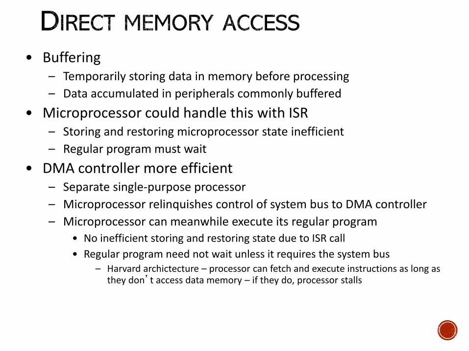
• Buffering– Temporarily storing data in memory before processing
– Data accumulated in peripherals commonly buffered
• Microprocessor could handle this with ISR– Storing and restoring microprocessor state inefficient
– Regular program must wait
• DMA controller more efficient– Separate single-purpose processor
– Microprocessor relinquishes control of system bus to DMA controller
– Microprocessor can meanwhile execute its regular program• No inefficient storing and restoring state due to ISR call
• Regular program need not wait unless it requires the system bus– Harvard archictecture – processor can fetch and execute instructions as long as
they don’t access data memory – if they do, processor stalls

• An additional module on the system bus, the DMA module, takes care of the I/O transfer for the whole sequence of data.
– The CPU issues a command to the DMA module and transfers to it all the needed information.
– When starting an operation, the CPU informs the DMA module about:
• what operation (read or write);
• the address of the I/O device involved;
• the starting location in memory where information has to be stored to or read from;
• the number of words to be transferred.
– The DMA module performs all the operations (acting similarly to the CPU with programmed I/O): it transfers all the data between I/O module and memory without going through the CPU.
– When the DMA module has finished, it issues an interrupt to the CPU.

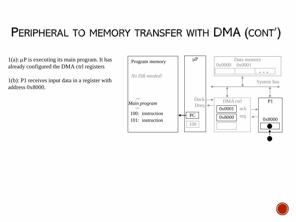
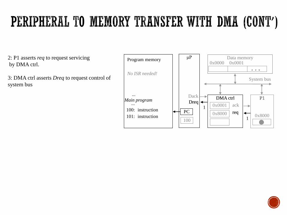
1(a): μP is executing its main program.
It has already configured the DMA ctrl
registers.
1(b): P1 receives input
data in a register with
address 0x8000.
2: P1 asserts req to request
servicing by DMA ctrl.
7(b): P1 de-asserts req.
Tim
e
3: DMA ctrl asserts Dreq
to request control of
system bus.
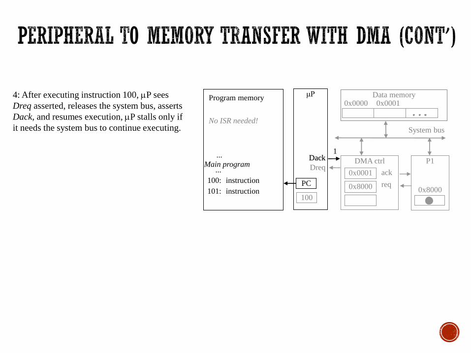
4: After executing instruction 100, μP
sees Dreq asserted, releases the system
bus, asserts Dack, and resumes
execution. μP stalls only if it needs the
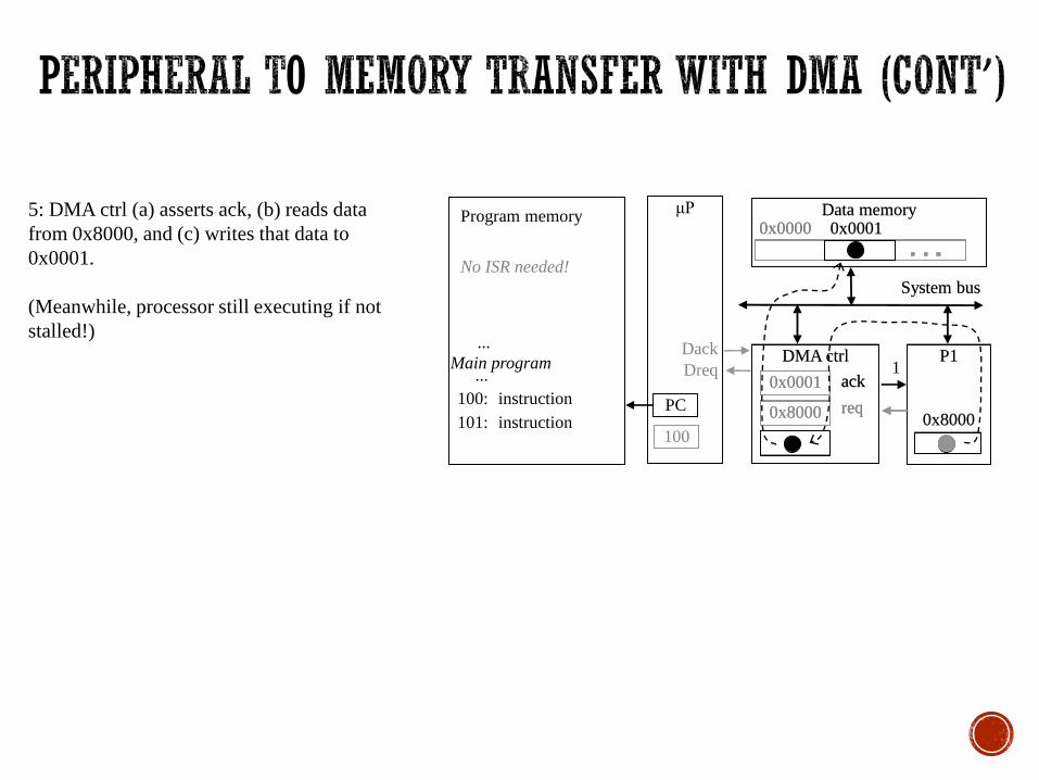
system bus to continue executing.5: (a) DMA ctrl asserts
ack (b) reads data from
0x8000 and (b) writes that
data to 0x0001.
6:. DMA de-asserts Dreq
and ack completing
handshake with P1. 7(a): μP de-asserts Dack and resumes
control of the bus.
1(a): P is executing its main program. It has
already configured the DMA ctrl registers
1(b): P1 receives input data in a register with
address 0x8000.
Data memoryμP
DMA ctrl P1
System bus
0x8000101:
instruction
instruction
...
Main program...
Program memory
PC
100
Dreq
Dack
0x0000 0x0001
100:
No ISR needed!
0x0001
0x8000
ack
req
2: P1 asserts req to request servicing
by DMA ctrl.
3: DMA ctrl asserts Dreq to request control of
system bus
Data memoryμP
DMA ctrl P1
System bus
0x8000101:
instruction
instruction
...
Main program...
Program memory
PC
100
Dreq
Dack
0x0000 0x0001
100:
No ISR needed!
0x0001
0x8000
ack
reqreq
1
P1Dreq
1
DMA ctrl P1
4: After executing instruction 100, P sees
Dreq asserted, releases the system bus, asserts
Dack, and resumes execution, P stalls only if
it needs the system bus to continue executing.
Data memoryμP
DMA ctrl P1
System bus
0x8000101:
instruction
instruction
...
Main program...
Program memory
PC
100
Dreq
Dack
0x0000 0x0001
100:
No ISR needed!
0x0001
0x8000
ack
req
Dack1
Data memoryμP
DMA ctrl P1
System bus
0x8000101:
instruction
instruction
...
Main program...
Program memory
PC
100
Dreq
Dack
0x0000 0x0001
100:
No ISR needed!
0x0001
0x8000
ack
req
Data memory
DMA ctrl P1
System bus
0x8000
0x0000 0x0001
0x0001
0x8000
ack
req
5: DMA ctrl (a) asserts ack, (b) reads data
from 0x8000, and (c) writes that data to
0x0001.
(Meanwhile, processor still executing if not
stalled!)
ack1

6: DMA de-asserts Dreq and ack completing
the handshake with P1.
Data memoryμP
DMA ctrl P1
System bus
0x8000101:
instruction
instruction
...
Main program...
Program memory
PC
100
Dreq
Dack
0x0000 0x0001
100:
No ISR needed!
0x0001
0x8000
ack
req
ack0Dreq
0
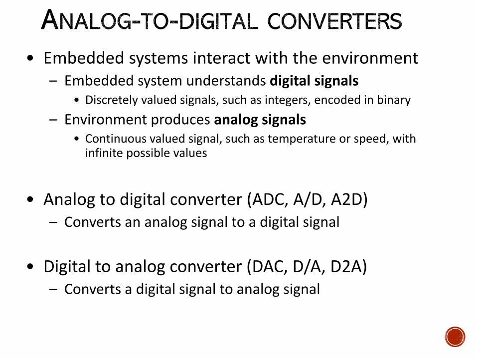
• Embedded systems interact with the environment– Embedded system understands digital signals
• Discretely valued signals, such as integers, encoded in binary
– Environment produces analog signals• Continuous valued signal, such as temperature or speed, with
infinite possible values
• Analog to digital converter (ADC, A/D, A2D)– Converts an analog signal to a digital signal
• Digital to analog converter (DAC, D/A, D2A)– Converts a digital signal to analog signal
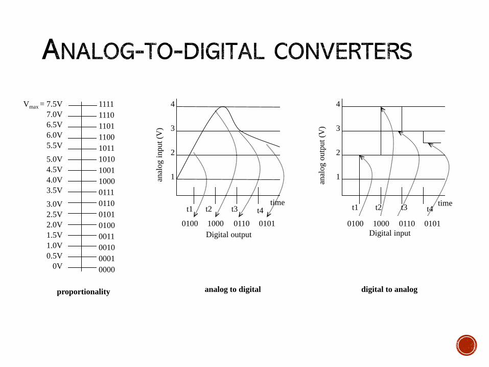
proportionality
Vmax = 7.5V
0V
1111
1110
0000
0010
0100
0110
1000
1010
1100
0001
0011
0101
0111
1001
1011
1101
0.5V
1.0V
1.5V
2.0V
2.5V
3.0V
3.5V
4.0V
4.5V
5.0V
5.5V
6.0V
6.5V
7.0V
analog to digital
4
3
2
1
t1 t2 t3 t4
0100 1000 0110 0101
time
anal
og i
nput
(V)
Digital output
digital to analog
4
3
2
1
0100 1000 0110 0101
t1 t2 t3 t4time
anal
og o
utp
ut
(V)
Digital input
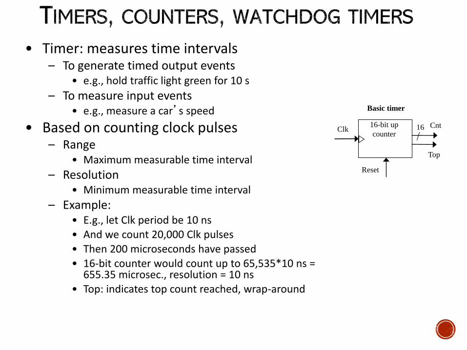
• Timer: measures time intervals– To generate timed output events
• e.g., hold traffic light green for 10 s
– To measure input events• e.g., measure a car’s speed
• Based on counting clock pulses– Range
• Maximum measurable time interval
– Resolution• Minimum measurable time interval
– Example:• E.g., let Clk period be 10 ns • And we count 20,000 Clk pulses• Then 200 microseconds have passed• 16-bit counter would count up to 65,535*10 ns =
655.35 microsec., resolution = 10 ns• Top: indicates top count reached, wrap-around
16-bit up
counterClk
Cnt
Basic timer
Top
Reset
16
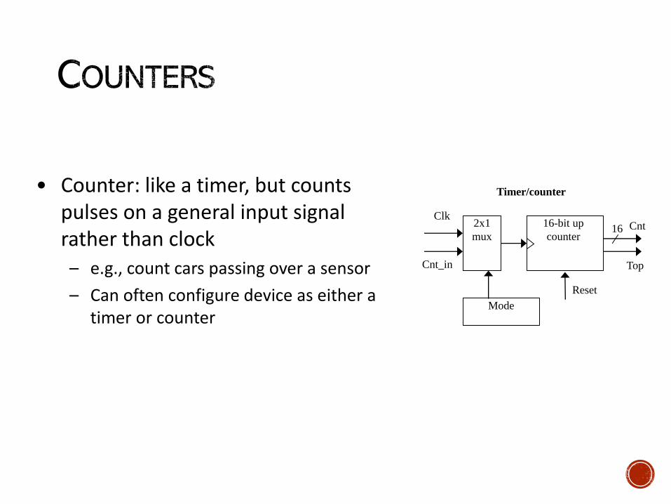
• Counter: like a timer, but counts pulses on a general input signal rather than clock
– e.g., count cars passing over a sensor
– Can often configure device as either a timer or counter
16-bit up
counter
Clk
16
Cnt_in
2x1
mux
Mode
Timer/counter
Top
Reset
Cnt

Top2
1. Interval timer– Indicates when desired
time interval has passed
– We set terminal count to desired interval
• Number of clock cycles = Desired time interval / Clock period
2. Cascaded counters
16-bit up
counterClk
16
Terminal count
=Top
Reset
(1) Timer with a
terminal count
Cnt
16-bit up
counterClk
16-bit up
counter
16
Cnt2
Top1
(2) 16/32-bit timer
Cnt1
16
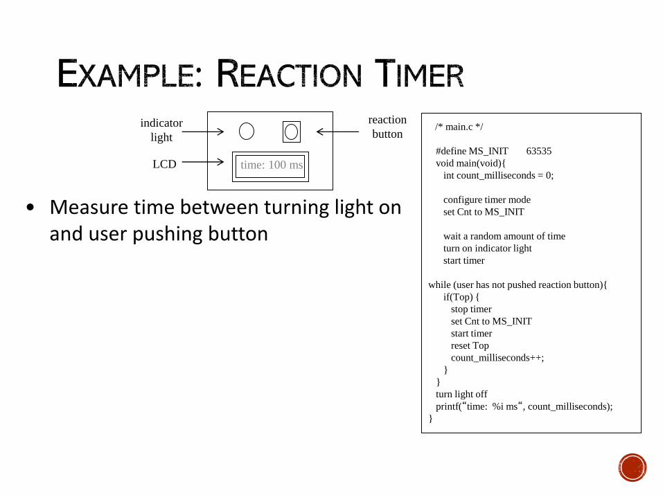
indicator
light
reaction
button
time: 100 msLCD
/* main.c */
#define MS_INIT 63535
void main(void){
int count_milliseconds = 0;
configure timer mode
set Cnt to MS_INIT
wait a random amount of time
turn on indicator light
start timer
while (user has not pushed reaction button){
if(Top) {
stop timer
set Cnt to MS_INIT
start timer
reset Top
count_milliseconds++;
}
}
turn light off
printf(“time: %i ms“, count_milliseconds);
}
• Measure time between turning light on and user pushing button

• Special kind of timer
– Must reset timer every X time unit, otherwise the watchdog timer generates a signal
– The watchdog timer “times-out” if we fail to reset it
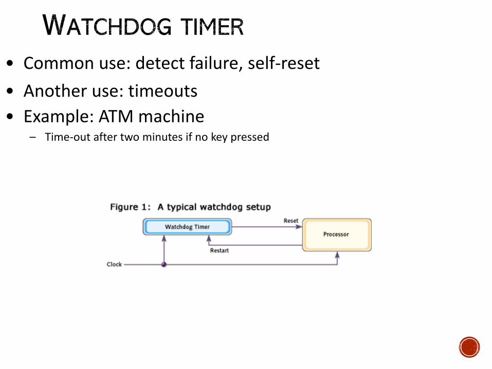
• Common use: detect failure, self-reset
• Another use: timeouts
• Example: ATM machine– Time-out after two minutes if no key pressed
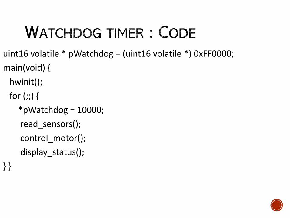
uint16 volatile * pWatchdog = (uint16 volatile *) 0xFF0000;
main(void) {
hwinit();
for (;;) {
*pWatchdog = 10000;
read_sensors();
control_motor();
display_status();
} }
• Logical fallacy, e.g., infinite loop– What if this happens with read_sensors()?
• Unusually high number of interrupts arrives – leads to dangerous delay in feeding the motor new control instructions
• Deadlocks that occur in multi-tasking kernels
• Note: failed hardware can lead to constant resets. So it is a good idea to count resets & give up after fixed number of failures

• PWM : a powerful technique to control analog circuits with a microprocessor’s digital output
• Essentially, it generates pulses with specific high/low times
• Duty cycle: % time high
– Square wave: 50% duty cycle

• Lamp connected to 9 V battery
• Switch on for 50 ms and then switch off for 50ms
• The lamp behaves as if it was powered by 4.5V source
• Duty cycle 50%
• Switching off and on frequency should be much higher than response time of the system
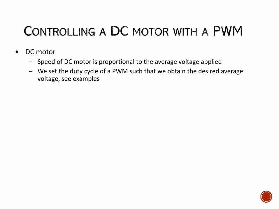
• DC motor– Speed of DC motor is proportional to the average voltage applied
– We set the duty cycle of a PWM such that we obtain the desired average voltage, see examples
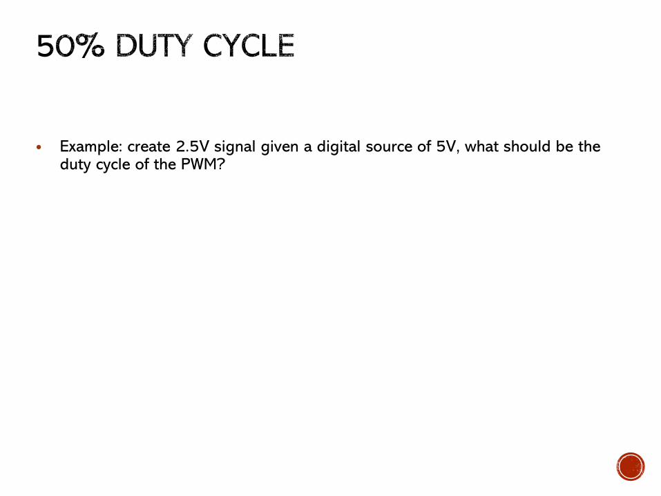
• Example: create 2.5V signal given a digital source of 5V, what should be the duty cycle of the PWM?
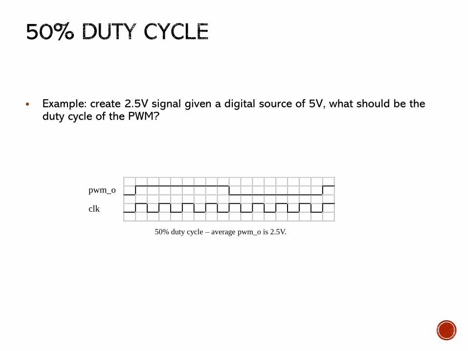
• Example: create 2.5V signal given a digital source of 5V, what should be the duty cycle of the PWM?
clk
pwm_o
50% duty cycle – average pwm_o is 2.5V.

• Example: create 1.25V signal given a digital source of 5V, what should be the duty cycle of the PWM?
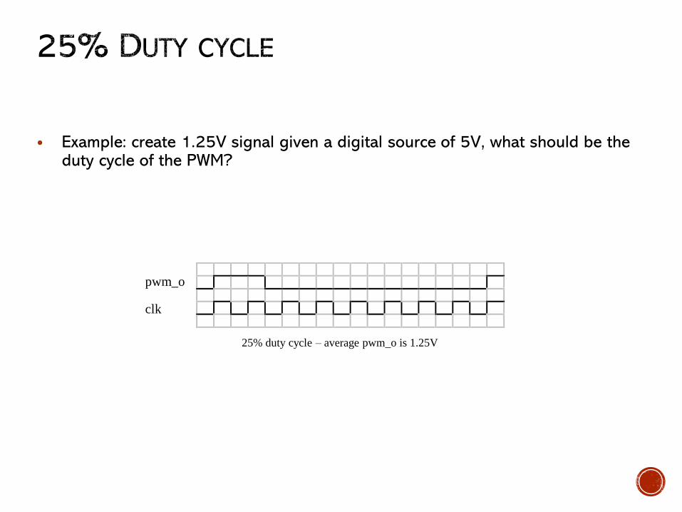
• Example: create 1.25V signal given a digital source of 5V, what should be the duty cycle of the PWM?
clk
pwm_o
25% duty cycle – average pwm_o is 1.25V

• Example: create 3.75V signal given a digital source of 5V, what should be the duty cycle of the PWM?
clk
pwm_o
75% duty cycle – average pwm_o is 3.75V.