design and applications of magnetic tunnel junction based ... · design and applications of...
TRANSCRIPT
Design and Applications of Magnetic TunnelJunction Based Logic Circuits
Hiwa Mahmoudi, Student Member, IEEE, Thomas Windbacher, Viktor Sverdlov,and Siegfried Selberherr, Fellow, IEEE
Institute for Microelectronics, Technische Universitat Wien, Gußhausstraße 27–29/E360,A-1040 Wien, Austria, Phone: +43-1-58801-36049, Fax: +43-1-58801-36099
E-mail: {mahmoudi|windbacher|sverdlov|selberherr}@iue.tuwien.ac.at
Abstract—By offering zero standby power, non-volatile logic isa promising solution to overcome the leakage current issue whichhas become an important obstacle, when CMOS technology isshrunk. Magnetic tunnel junction (MTJ)-based logic has a greatpotential, because of unlimited endurance, CMOS compatibility,and fast switching speed. Recently, several non-volatile MTJ-based circuits have been presented which inherently realizelogic-in-memory circuit concepts by using MTJ devices as bothmemory and the main computing elements. In this work wepresent a reliability simulation method for designing MTJ-basedlogic gates integrated with CMOS. As an application example,we study the reliability of a magnetic full adder in two differentdesigns based on the implication and the reprogrammable MTJlogic gates.
Index Terms—Logic-in-memory, material implication (IMP),magnetic tunnel junction (MTJ), non-volatile logic, spin transfertorque (STT)
I. INTRODUCTION
High standby power due to leakage currents has become animportant obstacle for scaling CMOS logic circuits (Fig. 1)at sub-100nm technologies [1]. A possible solution to over-come this problem is introducing non-volatility into the logiccircuits [2]. The Spin-transfer torque (STT) [3] switchingmagnetic tunnel junction (STT-MTJ) is one of the mostpromising non-volatile storage technologies, which combinesthe advantages of CMOS compatibility, high speed, highdensity, unlimited endurance, and scalability [4].
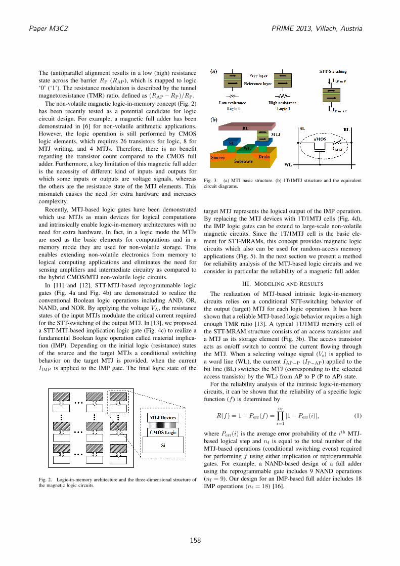
As shown in Fig. 2, distributing non-volatile memory ele-ments over the CMOS logic circuit plane (so-called logic-in-memory architecture [5]) can provide extremely low standbypower consumption and instant start-up by holding the in-formation in the MTJs and eliminating the need for refresh-ing pulses which are critical for CMOS-based memory ele-ments [6], [7], [8]. Furthermore, by using the MTJ technologythe effective area and interconnections delay (the data trafficon a main data bus between separated logic and memorymodules as shown in Fig. 1) can be reduced due to easy three-dimensional integration of the MTJs on top of the CMOSlayers (Fig. 2). However, in hybrid CMOS/MTJ circuits theMTJs are used only as ancillary devices which store thecomputation results [9]. Therefore, sensing amplifiers [10] arerequired for reading the data at each logic stage and providing
the next stage with an appropriate voltage or current signal asinput. This limitation increases the device count, delay, andpower consumption. Furthermore, the generalization to large-scale logic systems is problematic.
Recently, it has been demonstrated that STT-MTJs can bedirectly connected to perform logic operations [11], [12], [13],intrinsically enabling logic-in-memory architectures with noneed for extra hardware (also known as “stateful” logic [14]).Here, we show how the MTJ logic gates can be generalizedto large-scale logic systems based on one-transistor/one-MTJ(1T/1MTJ) cells (Fig. 3b) which are utilized as the basicmemory cells in the STT magnetoresistive random-accessmemory (STT-MRAM) structure [15].
II. INTRINSIC MTJ-BASED LOGIC-IN-MEMORY
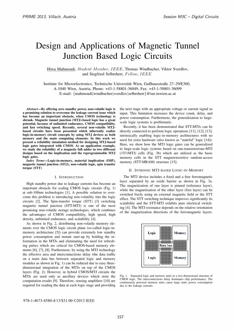
The MTJ device includes a fixed and a free ferromagneticlayer separated by an oxide barrier as shown in Fig. 3a.The magnetization of one layer is pinned (reference layer),while the magnetization of the other layer (free layer) can beswitched freely using an external magnetic field or the STTeffect. The STT switching technique improves significantly itsscalability and the STT-MTJ exhibits pure electrical switch-ing [4]. The MTJ resistance depends on the relative orientationof the magnetization directions of the ferromagnetic layers.
Fig. 1. Separated logic and memory units in a two-dimensional structure ofCMOS logic. The interconnections delay dominates chip performance. Thecontinuously powered memory units cause large static power consumptiondue to the leakage currents.
978-1-4673-4580-4/13/$31.00 ©2013 IEEE
PRIME 2013, Villach, Austria Session M3C – Digital Circuits
157
The (anti)parallel alignment results in a low (high) resistancestate across the barrier RP (RAP), which is mapped to logic‘0’ (‘1’). The resistance modulation is described by the tunnelmagnetoresistance (TMR) ratio, defined as (RAP−RP)/RP.
The non-volatile magnetic logic-in-memory concept (Fig. 2)has been recently tested as a potential candidate for logiccircuit design. For example, a magnetic full adder has beendemonstrated in [6] for non-volatile arithmetic applications.However, the logic operation is still performed by CMOSlogic elements, which requires 26 transistors for logic, 8 forMTJ writing, and 4 MTJs. Therefore, there is no benefitregarding the transistor count compared to the CMOS fulladder. Furthermore, a key limitation of this magnetic full adderis the necessity of different kind of inputs and outputs forwhich some inputs or outputs are voltage signals, whereasthe others are the resistance state of the MTJ elements. Thismismatch causes the need for extra hardware and increasescomplexity.
Recently, MTJ-based logic gates have been demonstratedwhich use MTJs as main devices for logical computationsand intrinsically enable logic-in-memory architectures with noneed for extra hardware. In fact, in a logic mode the MTJsare used as the basic elements for computations and in amemory mode they are used for non-volatile storage. Thisenables extending non-volatile electronics from memory tological computing applications and eliminates the need forsensing amplifiers and intermediate circuitry as compared tothe hybrid CMOS/MTJ non-volatile logic circuits.
In [11] and [12], STT-MTJ-based reprogrammable logicgates (Fig. 4a and Fig. 4b) are demonstrated to realize theconventional Boolean logic operations including AND, OR,NAND, and NOR. By applying the voltage VA, the resistancestates of the input MTJs modulate the critical current requiredfor the STT-switching of the output MTJ. In [13], we proposeda STT-MTJ-based implication logic gate (Fig. 4c) to realize afundamental Boolean logic operation called material implica-tion (IMP). Depending on the initial logic (resistance) statesof the source and the target MTJs a conditional switchingbehavior on the target MTJ is provided, when the currentIIMP is applied to the IMP gate. The final logic state of the
Fig. 2. Logic-in-memory architecture and the three-dimensional structure ofthe magnetic logic circuits.
Fig. 3. (a) MTJ basic structure. (b) 1T/1MTJ structure and the equivalentcircuit diagrams.
target MTJ represents the logical output of the IMP operation.By replacing the MTJ devices with 1T/1MTJ cells (Fig. 4d),the IMP logic gates can be extend to large-scale non-volatilemagnetic circuits. Since the 1T/1MTJ cell is the basic ele-ment for STT-MRAMs, this concept provides magnetic logiccircuits which also can be used for random-access memoryapplications (Fig. 5). In the next section we present a methodfor reliability analysis of the MTJ-based logic circuits and weconsider in particular the reliability of a magnetic full adder.
III. MODELING AND RESULTS
The realization of MTJ-based intrinsic logic-in-memorycircuits relies on a conditional STT-switching behavior ofthe output (target) MTJ for each logic operation. It has beenshown that a reliable MTJ-based logic behavior requires a highenough TMR ratio [13]. A typical 1T/1MTJ memory cell ofthe STT-MRAM structure consists of an access transistor anda MTJ as its storage element (Fig. 3b). The access transistoracts as on/off switch to control the current flowing throughthe MTJ. When a selecting voltage signal (Vs) is applied toa word line (WL), the current IAP−P (IP−AP) applied to thebit line (BL) switches the MTJ (corresponding to the selectedaccess transistor by the WL) from AP to P (P to AP) state.
For the reliability analysis of the intrinsic logic-in-memorycircuits, it can be shown that the reliability of a specific logicfunction (f ) is determined by
R(f) = 1− Perr(f) =
nf∏
i=1
[1− Perr(i)], (1)
where Perr(i) is the average error probability of the ith MTJ-based logical step and nf is equal to the total number of theMTJ-based operations (conditional switching evens) requiredfor performing f using either implication or reprogrammablegates. For example, a NAND-based design of a full adderusing the reprogrammable gate includes 9 NAND operations(nf = 9). Our design for an IMP-based full adder includes 18IMP operations (nf = 18) [16].
Paper M3C2 PRIME 2013, Villach, Austria
158

For a basic logic operation using MTJ gates, Perr is propor-tional to the sum of the switching probabilities for undesiredswitching events (Pu) and the term (1 − Pd) for the desiredswitching events as [13]
Perr =1
k + h
k∑
i=1
Pu(i) +h∑
j=1
1− Pd(j)
, (2)
where k and h are the number of the possible undesiredand desired switching events. According to the theoreticalmodel [17] and the measurements [15], the switching prob-ability (P ) of an MTJ in the thermally-activated switchingregime (switching time t >10 ns) is given by
P = 1− exp
{− t
τ0exp
[−∆0
(1− I
IC0
)]}, (3)
where ∆0 = E/kBT is the MTJ thermal stability factor, Iis the current flowing through the MTJ, t is the current pulseduration, τ0 ∼ 1ns, and IC0 is the critical switching currentextrapolated to τ0 [18].
In order to calculate the current passing through the MTJsin the 1T/1MTJ-based gate (Fig. 4d), we have
V iGS = VWL,
V j′
GS = VWL,V i
DS = VBL − V iM = VBL −Ri
MIiM,
V j′
DS = VBL −RGIj′
M − V j′
M = VBL − (RG +Rj′
M)I j′
M,
(4)
when the current IIMP is applied and the target and the sourcecells are selected by a voltage VWL applied to the ith and j′th
Fig. 4. Reprogrammable two-input (a) and three-input (b) MTJ-based logicgates [11], [12]. (c) Current-controlled MTJ-based implication logic gate [13].(d) 1T/1MTJ-based IMP logic circuit.
Fig. 5. The magnetic logic circuit based on the STT-MRAM architecture [13]with 1T/1MTJ cells (Fig. 3b) to realize intrinsic logic-in-memory for large-scale logic applications.
word lines (WLi and WLj′), respectively. Here, VGS (VDS) isthe voltage difference between the gate (drain) and the sourceof the access transistor, RM is the MTJ resistance, and IM isthe current through the MTJ device.
The R−V characteristics of the MTJ device is determinedby the voltage-dependent effective TMR model [19], if theMTJ is in the antiparallel state, as
RM = RAP = (1 + TMReff)RP = (1 +TMR0
1 +V 2M
V 2h
)RP, (5)
where TMR0 (TMReff ) is the TMR ratio under zero (non-zero) bias voltage (VM), and Vh is the bias voltage equivalentto TMReff = TMR0/2. The current passing through the ac-cess transistor (IM) satisfies [20]
IDS = IM = µnCoxW
L
[(VGS − VTH)VDS − V 2
DS
](6)
when the transistor is working in the triode (ohmic) region(VGS > VTH and VDS < VGS−VTH). Here, µn is the mobilityof electrons, Cox is the oxide thickness, and W (L) is thechannel width (length). For VDS > VGS − VTH (saturationregion), the channel exhibits pinch-off near drain and thecurrent can be approximated by the maximum value of (6)as [20]
IDS = IM =1
2µnCox
W
L(VGS − VTH)2. (7)
From a circuit point of view, for given MTJ device char-acteristics the value of the circuit parameters (VA, IIMP,and RG in Fig. 4) can be optimized to minimize Perr. Anexample of such an optimization for the MTJ-based gate ispresented in our previous work [13]. Based on (1)-(7), the
PRIME 2013, Villach, Austria Session M3C – Digital Circuits
159

200 250 300 350 40099
99.9
99.99
99.999
TMR Ratio (%)
FA
Reliability(%
)
Implication
Reprogrammable
Fig. 6. Reliability of the MTJ-based magnetic full adder as a function of theTMR ratio plotted for optimized circuit parameters and ∆0 = 60. The recordroom temperature TMR of 604% [21] promises highly reliable MTJ-basedlogic applications.
reliability of a magnetic full adder as a function of the TMRratio is plotted in Fig. 6 for IMP-based and reprogrammable-based implementations with optimized circuit parameters. Itdemonstrates that the reliability increases with the TMR forboth circuits. Due to a more reliable conditional switchingbehavior exhibited by the IMP gate, it provides a magneticfull adder with smaller error probability compared to thereprogrammable gates.
The 1T/1MTJ-based implementation of the intrinsic logic-in-memory gates can extend MRAM electronics from memoryto logical computing applications for complex logic func-tions. An IMP-based full adder design involves 27 subsequentFALSE and IMP operations [16] on 6 1T/1MTJ cells whichalready exist within the STT-MRAM structure (Fig. 5). Ascompared to the non-volatile full adder in [6], the need forCMOS-based logic is eliminated and superior logic densitycan be achieved.
IV. CONCLUSION
A method for reliability analysis of the MTJ-based logiccircuits is presented. As an example, the reliability of amagnetic full adder using IMP and reprogrammable gatesis considered. It is shown that the reliability improves withthe TMR for both designs and the IMP-based implementationexhibits a more reliable logic behavior. These structures canbe used to build more complex circuits which implementmore complex logic functions. Since the 1T/1MTJ cell canbe utilized as both memory and the main computing element,non-volatile intrinsic logic-in-memory can be realized withno need for intermediate circuitry. Circuits which exhibitlow power consumption, high logic density, and high speedoperation simultaneously can thus be designed.
ACKNOWLEDGMENT
The work is supported by the European Research Councilthrough the grant #247056 MOSILSPIN.
REFERENCES
[1] N. S. Kim, T. Austin, D. Baauw, T. Mudge, K. Flautner, J. S. Hu, M. J.Irwin, M. Kandemir, and V. Narayanan, “Leakage Current: Moore’s LawMeets the Static Power,” Computer, vol. 36, no. 12, pp. 68–75, 2003.
[2] S. Matsunaga, J. Hayakawa, S. Ikeda, K. Miura, T. Endoh, H. Ohno, andT. Hanyu, “MTJ-Based Nonvolatile Logic-in-Memory Circuit, FutureProspects and Issues,” Proc. Des. Autom. Test Eur. Conf. (DATE), pp.433–435, 2009.
[3] L. Berger, “Emission of Spin Waves by a Magnetic Multilayer Traversedby a Current,” Phys. Rev. B, Condens. Matter, vol. 54, pp. 9353–9358,1996.
[4] C. Chappert, A. Fert, and F. N. V. Dau, “The Emergence of SpinElectronics in Data Storage,” Nat. Mater., vol. 6, pp. 813–823, 2007.
[5] W. H. Kautz, “Cellular Logic-in-Memory Arrays,” IEEE Trans. Comput.,vol. C-18, no. 8, pp. 719–727, 1969.
[6] S. Matsunaga, J. Hayakawa, S. Ikeda, K. Miura, H. Hasegawa, T. Endoh,H. Ohno, and T. Hanyu, “Fabrication of a Nonvolatile Full Adder basedon Logic-in-Memory Architecture using Magnetic Tunnel Junctions,”Appl. Phys. Express, vol. 1, p. 091301, 2008.
[7] W. Zhao, E. Belhaire, C. Chappert, F. Jacquet, and P. Mazoyer, “NewNon-Volatile Logic Based on Spin-MTJ,” Phys. Status Solidi (a), vol.205, pp. 1373–1377, 2008.
[8] Y. Gang, W. Zhao, J. O. Klein, C. Chappert, and P. Mazoyer, “AHigh-Reliability, Low-Power Magnetic Full Adder,” IEEE Trans. Magn.,vol. 47, no. 11, pp. 4611–4616, 2011.
[9] W. Zhao, L. Torres, Y. Guillemenet, L. V. Cargnini, Y. Lakys, J.-O. Klein, D. Ravelosona, G. Sassatelli, and C. Chappert, “Design ofmram based logic circuits and its applications,” in ACM Great LakesSymposium on VLSI, 2011, pp. 431–436.
[10] W. Zhao, C. Chappert, V. Javerliac, and J.-P. Nozie, “High Speed, HighStability and Low Power Sensing Amplifier for MTJ/CMOS HybridLogic Circuits,” IEEE Trans. Magn., vol. 45, pp. 3784–3787, 2009.
[11] A. Lyle, J. Harms, S. Patil, X. Yao, D. Lilja, and J. P. Wang, “DirectCommunication Between Magnetic Tunnel Junctions for NonvolatileLogic Fan-out Architecture,” Appl. Phys. Lett., vol. 97, p. 152504, 2010.
[12] A. Lyle, S. Patil, J. Harms, B. Glass, X. Yao, D. Lilja, and J. P.Wang, “Magnetic Tunnel Junction Logic Architecture for Realization ofSimultaneous Computation and Communication,” IEEE Trans. Magn.,vol. 47, pp. 2970–2973, 2011.
[13] H. Mahmoudi, T. Windbacher, V. Sverdlov, and S. Selberherr, “Implica-tion Logic Gates using Spin-Transfer-Torque-Operated Magnetic TunnelJunctions for Intrinsic Logic-in-Memory,” Solid-State Electron., vol. 84,pp. 191–197, 2013.
[14] J. Borghetti, G. S. Snider, P. J. Kuekes, J. J. Yang, D. R. Stewart, andR. S. Williams, “Memristive Switches Enable Stateful Logic Operationsvia Material Implication,” Nature, vol. 464, no. 7290, pp. 873–876, 2010.
[15] M. Hosomi, H. Yamagishi, T. Yamamoto, K. Bessho, Y. Higo, K. Ya-mane, H. Yamada, M. Shoji, H. Hachinoa, C. Fukumoto, H. Nagao,and H. Kano, “A Novel Nonvolatile Memory with Spin Torque TransferMagnetization Switching: Spin-RAM,” IEDM Tech. Dig., pp. 459–462,2005.
[16] H. Mahmoudi, V. Sverdlov, and S. Selberherr, “A Robust and EfficientMTJ-based Spintronic IMP Gate for New Logic Circuits and Large-Scale Integration,” Proceedings of the 17th International Conferenceon Simulation of Semiconductor Processes and Devices (SISPAD), pp.225–228, 2012.
[17] Y. Higo, K. Yamane, K. Ohba, H. Narisawa, K. Bessho, M. Hosomi,and H. Kano, “Thermal Activation Effect on Spin Transfer Switchingin Magnetic Tunnel Junctions,” Appl. Phys. Lett., vol. 87, p. 082502,2005.
[18] J. D. Harms, F. Ebrahimi, X. F. Yao, and J. P. Wang, “SPICE Macro-model of Spin-Torque-Transfer-Operated Magnetic Tunnel Junctions,”IEEE Trans. Electron Devices, vol. 57, no. 6, pp. 1425–1430, 2010.
[19] Y. Zhang, W. Zhao, Y. Lakys, J. O. Klein, J. V. Kim, D. Ravelosona,and C. Chappert, “Compact Modeling of Perpendicular-AnisotropyCoFeB/MgO Magnetic Tunnel Junctions,” IEEE Trans. Electron De-vices, vol. 59, pp. 819–826, 2012.
[20] B. Razavi, Fundamentals of Microelectronics. Wiley, 2006.[21] S. Ikeda, J. Hayakawa, Y. Ashizawa, Y. M. Lee, K. Miura, H. Hasegawa,
M. Tsunoda, F. Matsukura, and H. Ohno, “Tunnel Magnetoresistance of604% at 300 K by Suppression of Ta Diffusion in CoFeB/MgO/CoFeBPseudo-Spin-Valves Annealed at High Temperature,” Appl. Phys. Lett.,vol. 93, p. 082508, 2008.
Paper M3C2 PRIME 2013, Villach, Austria
160