magnetic tunnel junctions for spintronics applications
TRANSCRIPT

Department of Electronics, AGH University of Science and Technology
Amorphous and Nanostructered Magnetic Materials – ANMM’2015, Iasi, 21 – 24 September 2015
T. Stobiecki
Department of Electronics AGH, Poland
Magnetic Tunnel Junctions for
spintronics applications
1

Department of Electronics, AGH University of Science and Technology
Amorphous and Nanostructered Magnetic Materials – ANMM’2015, Iasi, 21 – 24 September 2015
Spintronics devices road map
Technology of magnetic tunnel junctions (MTJs)• sputtering
• nanofabrication (electron-litography)
Magnetization dynamics Spin Transfer Torque (STT)
• Current-Induced Magnetization Switching (CIMS) in MTJs with
in-plane and out-of-plane anisotropy STT-RAM
• New underlayer materials for MTJs with out-of-plane anisotropy
Conclusions
Motivation Green I(nformation) T(echnology)
2
Outline
Spin Diode Effect
Spin Hall Effect (SHE) in Ta,W/CoFeB

Department of Electronics, AGH University of Science and Technology
Amorphous and Nanostructered Magnetic Materials – ANMM’2015, Iasi, 21 – 24 September 2015
Magnetoresistance
MR ratio (RT & low H)
AMR effect
MR = 1~2%
Year
1857
1990
1995
2000
2005
2015
Lord Kelvin
TMR effect
MR = 20~70%
1985GMR effect
MR = 5~15%
T. Miyazaki, J. Moodera STT J. Slonczewski, L. Berger 19661996
Device applications
HDD head
Inductive
head
MR head
GMR head
TMR head MRAM
Memory
Giant TMR effect
MR = 200~1000%
MgO -TMR headSpin Torque
MRAM Microwave, E-control,
Spin Orbit Torque
Novel
devices
1967
A. Fert, P. Grünberg, 2007 – Nobel Prize
3

Department of Electronics, AGH University of Science and Technology
Amorphous and Nanostructered Magnetic Materials – ANMM’2015, Iasi, 21 – 24 September 2015 4
10-5
10-4
10-3
10-2
10-1
100
101
10-7
10-6
10-5
10-4
10-3
10-2
10-1
100
101
102
103
104
105
MTJ size (m2)
Samsung 2011
Avalanche 2010
MagIC-IBM 2010
TSMC&Qualcomm 2009
Toshiba2008 MagIC-IBM 2008
IBM2003
Everspin2010
Everspin2010Hitachi&Tohoku 2010
SONY 2005
Grandis 2010
Everspin 2010
Toshiba 2012
Wri
tin
g e
ne
rgy (
pJ/b
it)
MRAM
(Øersted field)
Spin-transfer torque (STT) - RAM
Voltage effect
STT+voltage effect
MRAM
STT-RAM
GREEN IT, Present status of writing energy for MRAM
Energy requiredfor data retention
(60 kBT)
Φ30nm Φ100nm
Target < 1 fJ/bitΦ10nm
Electric-currentbased control
after T. Nozaki AIST

Department of Electronics, AGH University of Science and Technology
Amorphous and Nanostructered Magnetic Materials – ANMM’2015, Iasi, 21 – 24 September 2015
Green IT
after S. Yuasa (2012)
5

Department of Electronics, AGH University of Science and Technology
Amorphous and Nanostructered Magnetic Materials – ANMM’2015, Iasi, 21 – 24 September 2015
Green IT
after S. Yuasa (2012)
6

Department of Electronics, AGH University of Science and Technology
Amorphous and Nanostructered Magnetic Materials – ANMM’2015, Iasi, 21 – 24 September 2015
Tunneling – Julliere’s model
Ferromagnetic-electrode 1 Ferromagnetic-electrode 2Insulator
7

Department of Electronics, AGH University of Science and Technology
Amorphous and Nanostructered Magnetic Materials – ANMM’2015, Iasi, 21 – 24 September 2015
Magnetic field switching
TMR = 100%
AP
P
8
Resistance switching by external magnetic field

Department of Electronics, AGH University of Science and Technology
Amorphous and Nanostructered Magnetic Materials – ANMM’2015, Iasi, 21 – 24 September 2015
TMR = 100%
Curent Induced Magnetization Switching - CIMS
Resistance switching ? → by spin polarized current from SpinTransfer Torque (STT)
„1”
„0”
AP
P
9

Department of Electronics, AGH University of Science and Technology
Amorphous and Nanostructered Magnetic Materials – ANMM’2015, Iasi, 21 – 24 September 2015
(001)MgO
FFT
Transmission electron Microscopy (TEM) of TMR multilayers
TEM EDX
L. Yiao, S. van Dijken Aalto Univ.
0.9nm
2.3
0.6 – 1.1
2.3
3
50
3
50
3
16
2
0.9
7
30
10
+ AF
10
details in poster P-5-39

Department of Electronics, AGH University of Science and Technology
Amorphous and Nanostructered Magnetic Materials – ANMM’2015, Iasi, 21 – 24 September 2015
Courtesy of
Singulus TIMARISMulti Target Module
Top: Target Drum with 10
rectangular cathodes; Drum
design ensures easy
maintenance;
Bottom: Main part of the
chamber containing LDD
equipment
Oxidation ModuleLow Energy Remote
Atomic Plasma Oxidation;
Natural Oxidation;
Soft Energy Surface
Treatment
Transport Module
(UHV wafer handler)
Soft-Etch Module
(PreClean, Surface
Treatment)
Cassette Module
(according to
Customer request)
Ultra – High – Vacuum Design: Base Pressure 5*10-9 Torr (Deposition Chamber)
High Throughput (e.g. MRAM): 9 Wafer/Hour (1 Depo-Module)
High Effective Up-time: 18 Wafer/Hour (2 Depo-Module)
Sputtering deposition (industrial process)
11
Department of Electronics, AGH University of Science and Technology
Amorphous and Nanostructered Magnetic Materials – ANMM’2015, Iasi, 21 – 24 September 2015
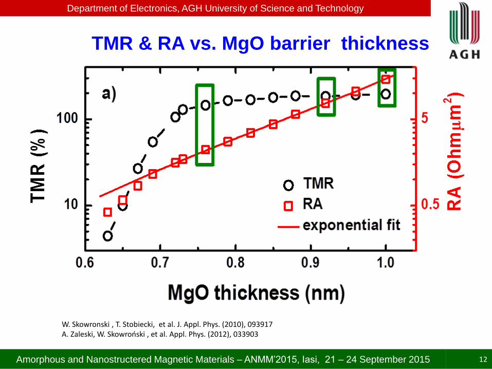
TMR & RA vs. MgO barrier thickness
W. Skowronski , T. Stobiecki, et al. J. Appl. Phys. (2010), 093917A. Zaleski, W. Skowroński , et al. Appl. Phys. (2012), 033903
12

Department of Electronics, AGH University of Science and Technology
Amorphous and Nanostructered Magnetic Materials – ANMM’2015, Iasi, 21 – 24 September 2015
Nanofabrication by electron-beam lithography
-1.0 -0.5 0.0 0.5 1.0
100
150
200
250
300
Resis
tance [O
hm
]
Voltage [V]
Nanopillar 3 step: e-beam litography, ion etching, lift-off
e-litography by RAITH system
13

Department of Electronics, AGH University of Science and Technology
Amorphous and Nanostructered Magnetic Materials – ANMM’2015, Iasi, 21 – 24 September 2015 14
Microsystem Ion sys 500 – Ar+ etching
Ta
RuCoFeB
MgO
Mass spectrometer
Nanofabrication by electron-beam lithography

Department of Electronics, AGH University of Science and Technology
Amorphous and Nanostructered Magnetic Materials – ANMM’2015, Iasi, 21 – 24 September 2015
dt
dmmHm
dt
dmeff
Magnetization dynamics LLG
precession damping
L(andau) L(ifszic) G(ilbert) dynamics
15

Department of Electronics, AGH University of Science and Technology
Amorphous and Nanostructered Magnetic Materials – ANMM’2015, Iasi, 21 – 24 September 2015
Spin Transfer Torque (STT)
Unpolarized
electrons
Polarized
electrons
Transmitted
electrons
Polarizer P Free layer M
Local magnetizationConduction Electrons Transfer of transverse
moment m
=
Torque
(Spin Torque ST)
ST tends to align M (anti-)parallel to P
Electron
flow
16

Department of Electronics, AGH University of Science and Technology
Amorphous and Nanostructered Magnetic Materials – ANMM’2015, Iasi, 21 – 24 September 2015
dt
dmmHm
dt
dmeff Mm
VolMMmm
VolM SS
)(||
precession dampingSTT
Spin Transfer Torque (STT)
17
Z
X=X’
Y
ZZ’ Y
Y’
Tunnel barrier
Free layer
Reference layer
θθ
𝝉⊥
𝝉∥
𝒎
𝑴
V >
0
𝐞−
Department of Electronics, AGH University of Science and Technology
Amorphous and Nanostructered Magnetic Materials – ANMM’2015, Iasi, 21 – 24 September 2015
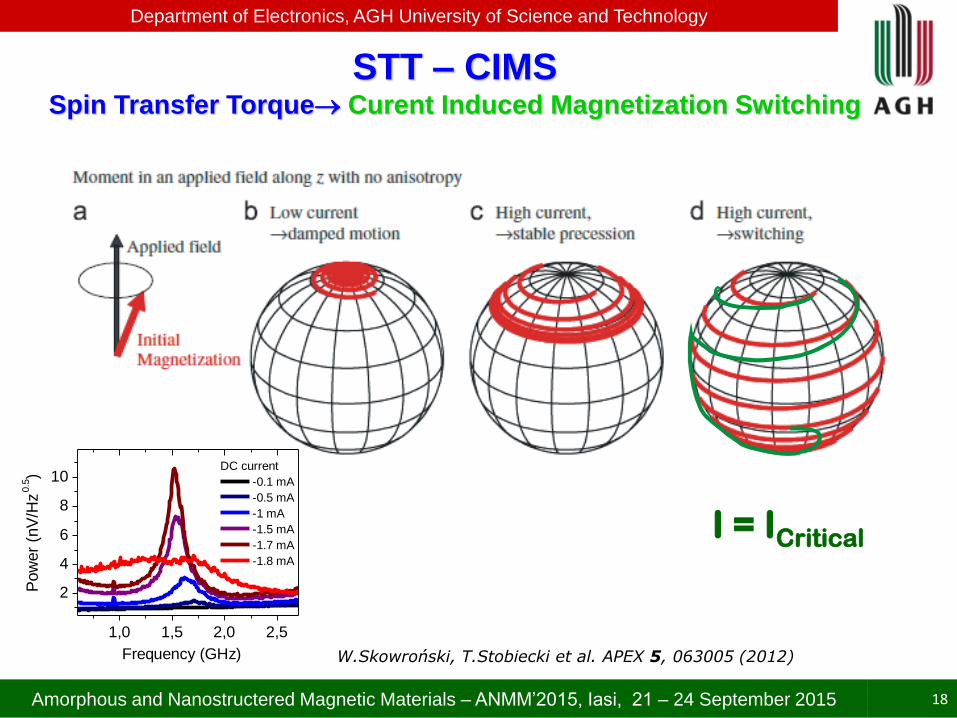
STT – CIMSSpin Transfer Torque Curent Induced Magnetization Switching
I = ICritical
1,0 1,5 2,0 2,5
2
4
6
8
10
Pow
er
(nV
/Hz
0.5)
Frequency (GHz)
DC current
-0.1 mA
-0.5 mA
-1 mA
-1.5 mA
-1.7 mA
-1.8 mA
W.Skowroński, T.Stobiecki et al. APEX 5, 063005 (2012)
18

Department of Electronics, AGH University of Science and Technology
Amorphous and Nanostructered Magnetic Materials – ANMM’2015, Iasi, 21 – 24 September 2015
Zero-magnetic field STO
• Use of:– Perpendicular anisotropy of thin CoFeB on MgO
– Needed Ferromagnetic coupling between FL and RL (0.9 nm
MgO)
• In-plane STT-induced oscillations
W.Skowroński, T.Stobiecki et al. APEX 5, 063005 (2012)
19

Department of Electronics, AGH University of Science and Technology
Amorphous and Nanostructered Magnetic Materials – ANMM’2015, Iasi, 21 – 24 September 2015 20
out-of-plane component
-1.0 -0.5 0.0 0.5 1.0
-2
-1
0
1
2 1 nm MgO
0.9 nm MgO
(1
0-19 N
m)
I (mA)
W.Skowroński, T.Stobiecki et al. PRB 87, 094419 (2013) Heiliger, Stiles PRL 100, 186805, (2008)
-1.0 -0.5 0.0 0.5 1.0
-2
-1
0
1
2
(
10-1
9 Nm
)
I (mA)
||
||
ab initio calculations
Perpendicular torque is about 10 times smaller than torque in plane ||
in-plane component

Department of Electronics, AGH University of Science and Technology
Amorphous and Nanostructered Magnetic Materials – ANMM’2015, Iasi, 21 – 24 September 2015 21
CIMS – critical current Jc0 in MTJ with in-plane
anisotropy• MTJ with 0.96 nm MgO
barrier and CoFeB free layer2.3 nm
0
0 ln2
1τ
τ
VMH
TkJJ P
SC
Bcc
3536
P APAP PStability factor
exp2
Tk
VMH
B
SC
W.Skowroński, T.Stobiecki et al. JAP 107, 093917 (2010)
-1.0 -0.5 0.0 0.5 1.0
400
600
800
1000
P P
AP 1 ms
2.7 ms
7.3 ms
19.8 ms
53.7 ms
b)
R
esis
tan
ce (
Oh
m)
Voltage (V)
AP

Department of Electronics, AGH University of Science and Technology
Amorphous and Nanostructered Magnetic Materials – ANMM’2015, Iasi, 21 – 24 September 2015 22
MTJ with perpendicular anisotropy
0.0 0.2 0.4 0.6 0.8 1.0 1.2 1.4 1.6
0.0
0.2
0.4
0.6
0.8
1.0
1.2
1.4
1.6
1.8
2.0 5Ta/10Ru/3Ta/0.75-1.25 FeCoB/1.28 MgO/5Ta/5Ru
5Ta/10Ru/3Ta/1.28 MgO/1.00-1.70 FeCoB/5Ta/5Ru
td = 0.75 nm
td = 1.07 nm
M/A
[em
u/c
m2]*
10
-5
FeCoB nominal thickness [nm]
0.0 0.1 0.2 0.3 0.4 0.5 0.6 0.7 0.8 0.9 1.0
-0.2
-0.1
0.0
0.1
0.2
0.3
0.4
0.5
0.6 5Ta/10Ru/3Ta/0.75-1.25 FeCoB/1.28 MgO/5Ta/5Ru
5Ta/10Ru/3Ta/1.28 MgO/1.00-1.70 FeCoB/5Ta/5Ru
K*t
eff
ective [
mJ/m
2]
CoFeB effective thickness [nm]
KV = -5.33*10
5 [J/m
3]
KS = 3.40*10
-4 [J/m
2]
tt = 0.64 nm
KV = -5.30*10
5 [J/m
3]
KS = 0.78*10
-4 [J/m
2]
tt = 0.15 nm
Kv
Ks
Kefft = KVt + KS
details in oral presentation O-4-02

Department of Electronics, AGH University of Science and Technology
Amorphous and Nanostructered Magnetic Materials – ANMM’2015, Iasi, 21 – 24 September 2015 23
0 2 4 6 8 10 12 14 16 18 20-2,0
-1,6
-1,2
-0,8
-0,4
0,0
0,4
0,8
1,2
1,6
2,0
Jc [M
A/c
m2
]
ln (tp/to)
effS
B
C VHMe
I
0
Critical current
2eff a SH H M M in plane
4eff a SH H M
M out of plane
Perpendicular magnetization reduces the critical switching current several times!
CIMS critical current in MTJs with
perpendicular anisotropy
Jc0 = 7MA/cm2
Jc0 = -15MA/cm2
Jc0 = 1.3MA/cm2
Jc0 = -1.2MA/cm2
Stability factor= 63
M. Frankowski, T.Stobiecki et.al JAP, 117,223908 (2015)

Department of Electronics, AGH University of Science and Technology
Amorphous and Nanostructered Magnetic Materials – ANMM’2015, Iasi, 21 – 24 September 2015 24
Influence of under layer materials on perpendicular magnetic anisotropy and VCMA effect
W. Skowroński, T. Nozaki et al. Phys. Rev. B 91, 184410 (2015)
Under layer: X (5 nm)
(CoFe)80B20 (0.88 nm)
MgO (2.5 nm)
Ta (5 nm)
(CoFe)80B20 Ref.
Ta (5 nm)
Ru (5 nm)
X: Ag, Ir, CuN, Zr, Nb, W 100 150 200 250 300 350 400 450 5000
20
40
60
80
Ag
Ir
CuN
Zr
Nb
W
Slo
pe
of
vo
lta
ge
eff
ec
t (f
J/V
m)
Annealing temperature (oC)
100 200 300 400 500
-5
0
5
10 Ag
Ir
CuN
Zr
Nb
W
Hp
erp
,eff (
kO
e)
Annealing temperature (C)
• Ir buffer shows the largest anisotropy change with the high PMA of Ki,0=1.9 mJ/m2, but low annealing stability
• W buffer exhibits high annealing stability up to 450 oC with keeping high PMA and VCMA effect of about 50 fJ/Vm
200 250 300 350 400 450
0
10
20
30
40
50
60
Annealing Temperature (oC)
TM
R (
%)
Ag
Ir
CuN
Zr
Nb
W

Department of Electronics, AGH University of Science and Technology
Amorphous and Nanostructered Magnetic Materials – ANMM’2015, Iasi, 21 – 24 September 2015 25
Mixing RF current with oscillatingresistancegive DC component
Spin Diode Effect induced by Magnetic Field or STT
𝛿𝜃
0
10
5
10
-1
0
1
0 200 400 600
Vdc
Time
RF current
Oscillatingresistance
Spin diode DC voltage
𝛿𝑅
𝑅(𝜃0)
2 m
Bottom Top
BiasT
V
280 nm
520 nm
STT
A. Tulapurkar et al. Nature 438 , 339–342 (2005).

Department of Electronics, AGH University of Science and Technology
Amorphous and Nanostructered Magnetic Materials – ANMM’2015, Iasi, 21 – 24 September 2015 26
107
108
109
-6
-4
-2
0
2
4
VD
C[m
V]
Frequency [Hz]
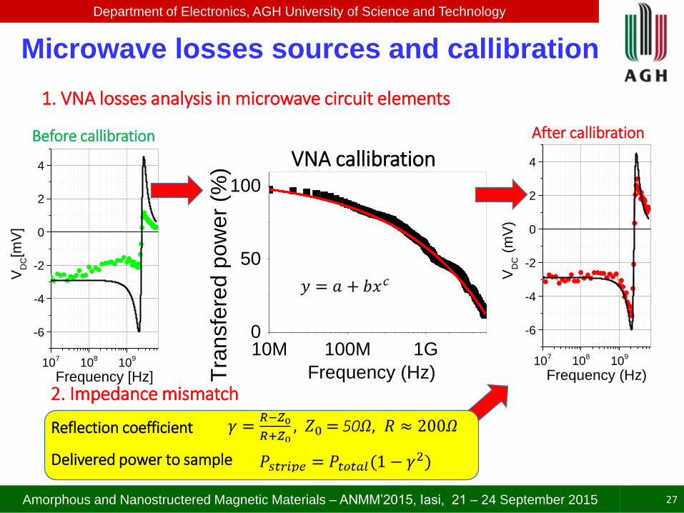
Microwave losses sources and callibration
Department of Electronics, AGH University of Science and Technology
Amorphous and Nanostructered Magnetic Materials – ANMM’2015, Iasi, 21 – 24 September 2015 27
1. VNA losses analysis in microwave circuit elements
107
108
109
-6
-4
-2
0
2
4
VD
C[m
V]
Frequency [Hz]10
710
810
9
-6
-4
-2
0
2
4
VD
C (
mV
)
Frequency (Hz)
Before callibration After callibration
2. Impedance mismatch
Microwave losses sources and callibration
VNA callibration
10M 100M 1G0
50
100
Tra
nsfe
red
pow
er
(%)
Frequency (Hz)
Reflection coefficient
Delivered power to sample

Department of Electronics, AGH University of Science and Technology
Amorphous and Nanostructered Magnetic Materials – ANMM’2015, Iasi, 21 – 24 September 2015 28
𝑉𝑜𝑢𝑡 = 𝑉𝑑𝑐+ 𝑉𝑎𝑐= 𝛿𝑅𝑐𝑜𝑠 𝜔𝑡 + 𝛽 ×𝑉
𝑅 𝜃0cos 𝜔𝑡
=𝑉𝛿𝑅
2𝑅(𝜃0)𝑐𝑜𝑠𝛽 + cos(2𝜔𝑡 + 𝛽)
M. Harder, et al., Phys. Rev. B 84, 054423 (2011)T. Nozaki, et al., Nat. Phys. 8, 491 (2012),S. Ziętek, P. Ogrodnik, T. Stobiecki, J. Barnaś et al., Phys. Rev. B 91, 014430 (2015)
timeindependent
timedependent
Spin diode effect theory

Department of Electronics, AGH University of Science and Technology
Amorphous and Nanostructered Magnetic Materials – ANMM’2015, Iasi, 21 – 24 September 2015 29
𝑉𝑑𝑐=𝑉𝛿𝑅
2𝑅(𝜃0)𝑐𝑜𝑠𝛽
𝑉𝑜𝑢𝑡 = 𝑉𝑑𝑐+ 𝑉𝑎𝑐= 𝛿𝑅𝑐𝑜𝑠 𝜔𝑡 + 𝛽 ×𝑉
𝑅 𝜃0cos 𝜔𝑡
=𝑉𝛿𝑅
2𝑅(𝜃0)𝑐𝑜𝑠𝛽 + cos(2𝜔𝑡 + 𝛽)
timeindependent
timedependent
M. Harder, et al., Phys. Rev. B 84, 054423 (2011)T. Nozaki, et al., Nat. Phys. 8, 491 (2012),S. Ziętek, P. Ogrodnik, T. Stobiecki, J. Barnaś et al., Phys. Rev. B 91, 014430 (2015)
Spin diode effect theory
Department of Electronics, AGH University of Science and Technology
Amorphous and Nanostructered Magnetic Materials – ANMM’2015, Iasi, 21 – 24 September 2015 30
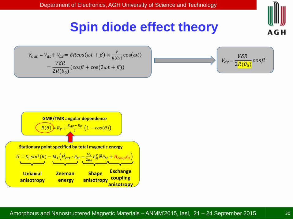
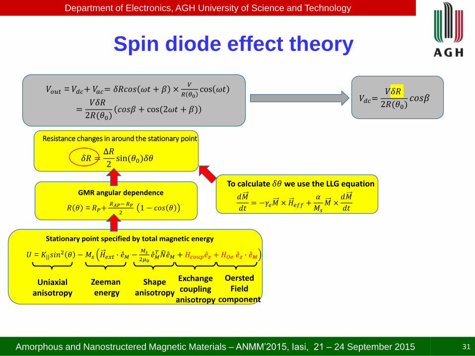
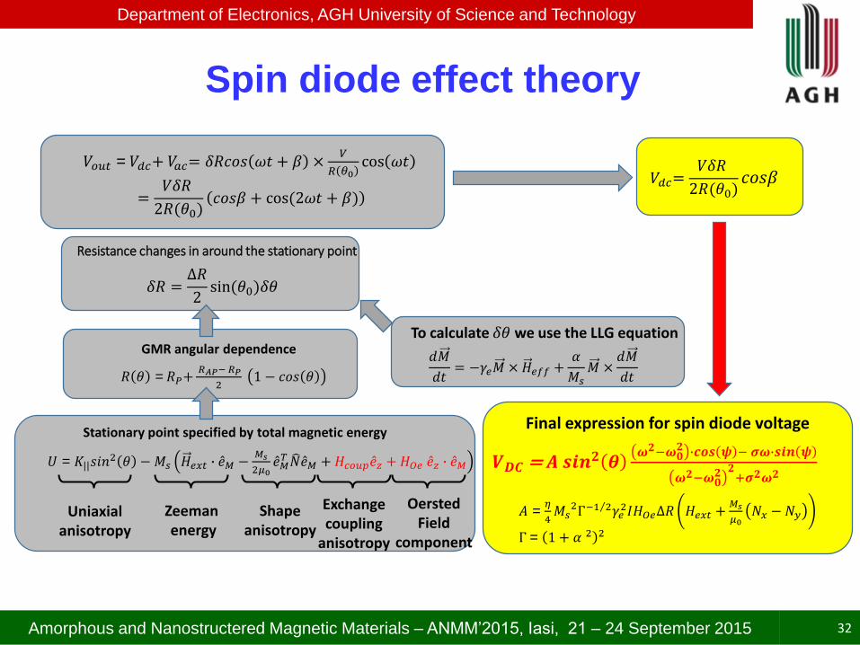
𝑅 𝜃 = 𝑅𝑃+𝑅𝐴𝑃− 𝑅𝑃
21 − 𝑐𝑜𝑠 𝜃
GMR/TMR angular dependence
𝑈 = 𝐾||𝑠𝑖𝑛2 𝜃 − 𝑀𝑠 𝐻𝑒𝑥𝑡 ∙ 𝑒𝑀 −
𝑀𝑠
2𝜇0 𝑒𝑀𝑇 𝑁 𝑒𝑀 + 𝐻𝑐𝑜𝑢𝑝 𝑒𝑧
Stationary point specified by total magnetic energy
Uniaxialanisotropy
Zeemanenergy
Shapeanisotropy
𝑉𝑜𝑢𝑡 = 𝑉𝑑𝑐+ 𝑉𝑎𝑐= 𝛿𝑅𝑐𝑜𝑠 𝜔𝑡 + 𝛽 ×𝑉
𝑅 𝜃0cos 𝜔𝑡
=𝑉𝛿𝑅
2𝑅(𝜃0)𝑐𝑜𝑠𝛽 + cos(2𝜔𝑡 + 𝛽)
Exchange coupling
anisotropy
𝑉𝑑𝑐=𝑉𝛿𝑅
2𝑅(𝜃0)𝑐𝑜𝑠𝛽
Spin diode effect theory
Department of Electronics, AGH University of Science and Technology
Amorphous and Nanostructered Magnetic Materials – ANMM’2015, Iasi, 21 – 24 September 2015 31
𝑅 𝜃 = 𝑅𝑃+𝑅𝐴𝑃− 𝑅𝑃
21 − 𝑐𝑜𝑠 𝜃
GMR angular dependence
𝑈 = 𝐾||𝑠𝑖𝑛2 𝜃 − 𝑀𝑠 𝐻𝑒𝑥𝑡 ∙ 𝑒𝑀 −
𝑀𝑠
2𝜇0 𝑒𝑀𝑇 𝑁 𝑒𝑀 + 𝐻𝑐𝑜𝑢𝑝 𝑒𝑧 + 𝐻𝑂𝑒 𝑒𝑧 ∙ 𝑒𝑀
Stationary point specified by total magnetic energy
Uniaxialanisotropy
Zeemanenergy
Shapeanisotropy
𝑉𝑜𝑢𝑡 = 𝑉𝑑𝑐+ 𝑉𝑎𝑐= 𝛿𝑅𝑐𝑜𝑠 𝜔𝑡 + 𝛽 ×𝑉
𝑅 𝜃0cos 𝜔𝑡
=𝑉𝛿𝑅
2𝑅(𝜃0)𝑐𝑜𝑠𝛽 + cos(2𝜔𝑡 + 𝛽)
Exchange coupling
anisotropy
To calculate 𝛿𝜃 we use the LLG equation
𝑑𝑀
𝑑𝑡= −𝛾𝑒𝑀 ×𝐻𝑒𝑓𝑓 +
𝛼
𝑀𝑠𝑀 ×
𝑑𝑀
𝑑𝑡
Resistance changes in around the stationary point
𝛿𝑅 =Δ𝑅
2sin(𝜃0)𝛿𝜃
Oersted Field
component
𝑉𝑑𝑐=𝑉𝛿𝑅
2𝑅(𝜃0)𝑐𝑜𝑠𝛽
Spin diode effect theory
Department of Electronics, AGH University of Science and Technology
Amorphous and Nanostructered Magnetic Materials – ANMM’2015, Iasi, 21 – 24 September 2015 32
𝑅 𝜃 = 𝑅𝑃+𝑅𝐴𝑃− 𝑅𝑃
21 − 𝑐𝑜𝑠 𝜃
GMR angular dependence
𝑈 = 𝐾||𝑠𝑖𝑛2 𝜃 − 𝑀𝑠 𝐻𝑒𝑥𝑡 ∙ 𝑒𝑀 −
𝑀𝑠
2𝜇0 𝑒𝑀𝑇 𝑁 𝑒𝑀 + 𝐻𝑐𝑜𝑢𝑝 𝑒𝑧 + 𝐻𝑂𝑒 𝑒𝑧 ∙ 𝑒𝑀
Stationary point specified by total magnetic energy
Uniaxialanisotropy
Zeemanenergy
Shapeanisotropy
𝑉𝑜𝑢𝑡 = 𝑉𝑑𝑐+ 𝑉𝑎𝑐= 𝛿𝑅𝑐𝑜𝑠 𝜔𝑡 + 𝛽 ×𝑉
𝑅 𝜃0cos 𝜔𝑡
=𝑉𝛿𝑅
2𝑅(𝜃0)𝑐𝑜𝑠𝛽 + cos(2𝜔𝑡 + 𝛽)
Exchange coupling
anisotropy
Resistance changes in around the stationary point
𝛿𝑅 =Δ𝑅
2sin(𝜃0)𝛿𝜃
Oersted Field
component
𝐴 = 𝜂
4𝑀𝑠
2Γ− 1 2𝛾𝑒2𝐼𝐻𝑂𝑒Δ𝑅 𝐻𝑒𝑥𝑡 +
𝑀𝑠
𝜇0𝑁𝑥 − 𝑁𝑦
Γ = 1 + 𝛼 2 2
Final expression for spin diode voltage
𝑽𝑫𝑪 = 𝑨 𝒔𝒊𝒏𝟐 𝜽𝝎𝟐−𝝎𝟎
𝟐 ∙𝒄𝒐𝒔 𝝍 − 𝝈𝝎∙𝒔𝒊𝒏 𝝍
𝝎𝟐−𝝎𝟎𝟐 𝟐
+𝝈𝟐𝝎𝟐
To calculate 𝛿𝜃 we use the LLG equation
𝑑𝑀
𝑑𝑡= −𝛾𝑒𝑀 ×𝐻𝑒𝑓𝑓 +
𝛼
𝑀𝑠𝑀 ×
𝑑𝑀
𝑑𝑡
𝑉𝑑𝑐=𝑉𝛿𝑅
2𝑅(𝜃0)𝑐𝑜𝑠𝛽
Spin diode effect theory

Department of Electronics, AGH University of Science and Technology
Amorphous and Nanostructered Magnetic Materials – ANMM’2015, Iasi, 21 – 24 September 2015 33
1.8 2.0 2.2 2.4 2.6-50
0
50
Hco
up (
Oe)
Cu layer thickness (nm)
107
108
109
1010
-10
-5
0
5
107
108
109
1010
-10
-5
0
5
107
108
109
1010
-10
-5
0
5
196 Oe
61 Oe
32 Oe
Vd
c (
mV
)
Frequency (Hz)
AF „0” F
Vdc vs. Frequency at H = const
S. Zietek, T.Stobiecki, Appl.Phys.Lett. 107 (2015)

Department of Electronics, AGH University of Science and Technology
Amorphous and Nanostructered Magnetic Materials – ANMM’2015, Iasi, 21 – 24 September 2015 34
Optimization efficiency of spin diode effectSD efficiency for different Cu layer thickness
AMR [1] GMR [2] TMR [3]
Magnetoresistance [%] ~3% ~10% ~100%
Efficiency [V/W] 0.15 V/W ~0.3 - 2 V/W 11-1000V/W
Advantages / disadvantages
• Low efficiency• Cheap
fabrication
• Cheap fabrication• Relatively good
efficiency• Current in plain
• High efficiency• Complex fabrication
process• Easy to breakdown
[3] W. Skowroński, T. Stobiecki et al. Appl. Phys. Lett. 105, 072409 (2014)
[1] A. Yamaguchi, et al. Appl. Phys. Lett. 90, 182507 (2007)
[2] J. Kleinlein, et al., Appl. Phys. Lett. 104, 153507 (2014)
Department of Electronics, AGH University of Science and Technology
Amorphous and Nanostructered Magnetic Materials – ANMM’2015, Iasi, 21 – 24 September 2015 35
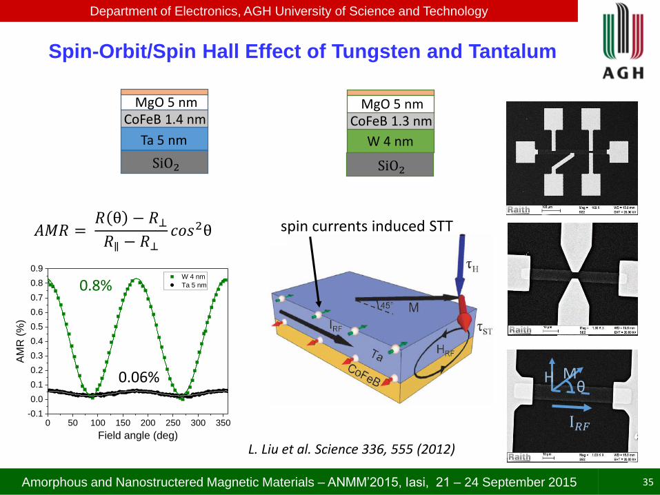
Spin-Orbit/Spin Hall Effect of Tungsten and Tantalum
Ta 5 nm
MgO 5 nmCoFeB 1.4 nm
SiO2
W 4 nm
MgO 5 nmCoFeB 1.3 nm
SiO2
𝐴𝑀𝑅 =𝑅 θ − 𝑅⊥𝑅∥ − 𝑅⊥
𝑐𝑜𝑠2θ
L. Liu et al. Science 336, 555 (2012)
0 50 100 150 200 250 300 350-0.1
0.0
0.1
0.2
0.3
0.4
0.5
0.6
0.7
0.8
0.9 W 4 nm
Ta 5 nm
AM
R (
%)
Field angle (deg)
0.06%
0.8%
spin currents induced STT
I𝑅𝐹
H Mθ
Department of Electronics, AGH University of Science and Technology
Amorphous and Nanostructered Magnetic Materials – ANMM’2015, Iasi, 21 – 24 September 2015
Cooperation and financial support
AGH Department of Electronics:
M. Czapkiewicz (micromagnetic simulations, magnetoptics)
J. Kanak (structure: XRD, AFM/MFM)
W. Skowronski (e-lithography ACMiN AGH, TMR, CIMS,Spin-diode, ST-FMR)
P. Wisniowski (MR-sensors, noise measurements and analysis)
W. Powroźnik (technical service)
M.Frankowski, PhD student (micromagnetic simulations)
M. Dąbek, PhD student (noise in sensors)
S. Ziętek PhD student (e-lithography, multiferroics)
M. Cecot, PhD student (SHE/SOT, AFM/MFM, e-lithography)
J. Chęciński, PhD student (micromagnetic simulations)
P. Rzeszut, student (LabView programming, electronic service, measurements)
ACMiN AGH: A. Żywczak (e-litography, PLD deposition, magnetic measurements)
Singulus AG: J. Wrona (sputtering deposition at Singulus AG, CIPT-capres measurements)
IFM PAN: J. Barnaś (UAM), P. Balaz (UAM, ChU Prag), J.Dubowik, H.Głowiński, P.Ogrodnik (PW), F.Stobiecki
AIST, Japan: T. Nozaki, S. Yuasa, Y.Suzuzki
EPFL, Switzerland: J-Ph. Ansermet, A.Vetro
University of Bielefeld, Germany : G. Reiss
Aalto University, Espoo, Finland: S. van Dijken
36

Department of Electronics, AGH University of Science and Technology
Amorphous and Nanostructered Magnetic Materials – ANMM’2015, Iasi, 21 – 24 September 2015 37
We acknowledge Polish National Science Center GrantNo. Harmonia-DEC-2012/04/M/ST7/00799
We acknowledge the NANOSPIN Grant no. PSPB- 045/2010 from Switzerland through the Swiss Contribution
Acknowledgments
Nanoscale spin torque devices for spin electronics

Department of Electronics, AGH University of Science and Technology
Amorphous and Nanostructered Magnetic Materials – ANMM’2015, Iasi, 21 – 24 September 2015
Conclusions
• Successful fabrication of MTJ nanopillars with an
ultrathin MgO barrier.
• Spin Transfer Torque (STT) effect in MTJs has been
quantitatively analysed.
• Current Induced Magnetization Switching (CIMS) and ST-
oscillations in MTJs with in-plane and out-of-plane
anisotropy have been demonstrated.
• New highly thermally stable underlayers, W and Ir with
high out of plane anisotropy and Voltage-Controled
Magnetic Anisotropy (VCMA) has been analyzed.
• The Spin Diode Effect has been demonstrated as a very
useful tool for magnetization dynamics investigations of
different spintronics devices: AMR, GMR,TMR and SHE.
38

Department of Electronics, AGH University of Science and Technology
Amorphous and Nanostructered Magnetic Materials – ANMM’2015, Iasi, 21 – 24 September 2015
Dziękuję za uwagę
39