mim tunnel junctions a thesis
TRANSCRIPT
DESIGN, FABRICATION AND CHARACTERIZATION OF
NANOMETER-SCALE VARIABLE-GEOMETRY
MIM TUNNEL JUNCTIONS
by
ELIZABETH A. MCKINNEY, B.S.E.E.
A THESIS
IN
ELECTRICAL ENGINEERING
Submitted to the Graduate Faculty
of Texas Tech University in Partial Fulfillment of the Requirements for
the Degree of
MASTER OF SCIENCE
IN
ELECTRICAL ENGINEERING
i^^roved
December, 2004

ACKNOWLEDGEMENTS
I would like to thank all of the individuals that have helped me in my academic
endeavors over the last two years: Dr. Gale for his thorough and insightful advice,
technical support, encouragement and the opportunity to be a part of this research project,
Dr. Temkin for his constructive criticism and technical advice and the Maddox lab
research facility and students for their technical advise and support. I have a special
thanks for Dr. Dallas and Judy Patterson for giving me the inspiration to complete my
degree and guiding me toward a field that I love. I would also like to thank my friends
and family for their unyielding love and support: Stephen Frisbie, Thomas Knapczyk,
Robert Anderson, Mary Donahue, and Adam Williamson for the many laughs and great
friendship, Rosalyn Manor for being a great teacher, an inspiration and a role model, my
parents, in-laws and grandparents for believing in me when times were tough. And most
of all, my husband Patrick for his understanding, support and unselfish nature, for his
unconditional love for me and my children, for being the best dad I know, and lastly, my
children, Kylee and Brayden, for the never-ending joy they bring to my life.
TABLE OF CONTENTS
ACKNOLEDGEMENTS ii
TABLi: OF CONTEN PS iii
ABSTRACT v
LIST OF FIGURES vi
CHAPTER
I. INTRODUCTION AND BACKGROUND 1
Motixation 1
Magnetoresistive Devices 2
Magnetic Readheads 2
Magnetic Random Access Memory 3
Relation of Magnetoresistance to MIM TJ 4
Quantum Theory 5
Wave properties of matter 7
II. NON-MAGNETIC TUNNEL JUNCTION DEVICE DESIGN 10
MIM Tunnel Junction Function 10
MIM Turmel Junction Structure 10
Device Layout and Fabrication 12
Fabrication Process Design 12
Thermal Oxidation - Process No. 1 14
E-Beam Evaporation - Process No. 2 16
Lithography 1 - Process No. 3 17
Anodization - Process No. 4 20
iii
Lift-off- Process No. 5 and 6 20
III. ANODIZATION OF ALUMINUM 24
Chemical Reaction 25
Anodization Procedure 27
Barrier Aluminum Oxide Characteristics 28
Film Growth Experiment 28
Film Thickness Determination 33
Profilometer Measurements 33
Interferometeric Imaging 34
SEM Imaging 36
IV. ELECTRICAL CHARACTERIZATION AND EXPERIMENTS 44
Measurement Setup 44
Probe Station 45
Keithley 2400 and LabVIEW 46
MIM Current-Voltage Characteristics 47
TJ Area Comparisons 50
Turmel Mechanism Determination 54
Oxide Thickness Dependence 58
V. CONCLUSIONS AND DISCUSSION 64
Project Summary 64
Future Work 65
REFERENCES 67
IV
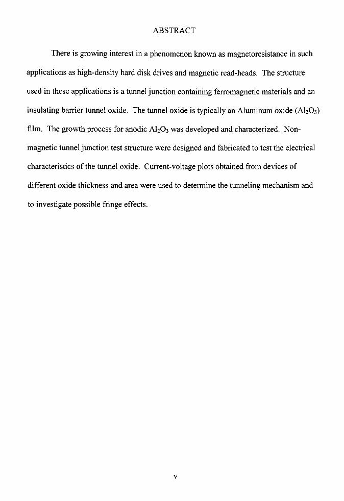
ABSTRACT
There is growing interest in a phenomenon known as magnetoresistance in such
applications as high-density hard disk drives and magnetic read-heads. The structure
used in these applications is a tunnel junction containing ferromagnetic materials and an
insulating barrier tunnel oxide. The turmel oxide is typically an Aluminum oxide (AI2O3)
film. The growth process for anodic AI2O3 was developed and characterized. Non
magnetic tunnel junction test structure were designed and fabricated to test the electrical
characteristics of the tunnel oxide. Current-voltage plots obtained from devices of
different oxide thickness and area were used to determine the tunneling mechanism and
to investigate possible fringe effects.

LIST OF FIGURES
1.1 Magnetic Tunnel Junction Layers 1
1.2 Magnetic Recording Process 3
1.3 MRAM Structure 4
1.4 Barrier Penetration'' 9
2.1 Cross-section of the MIM tunnel junction. Sizes not shown to scale 11
2.2 Plan \ lew of device (left) and cross-section of device (right) 11
2.3 Table of Process Steps (top) and Process Flow (bottom) 13
2.4 SEM Image of Si02 15
2.5 Photo-mask for Lithography Step No. 1 19
2.6 Lift-off Process Flow 21
2.7 Photo-mask for Lithography No. 2 22
2.8 Plan View Image of Device 23
3.1 Anodization Process Configuration 25
3.2 Ionic Current at Sample Surface 26
3.3 Anodization Growth Response for Vanod of 20 V 29
3.4 Anodization Current Response Modeling for Vanod of 20 V 30
3.5. 25-Voh Current Response 30
3.6 30-Volt Current Response 31
3.7 35-Volt Current Response 31
3.8 40-Voh Current Response 32
3.9 45-Vok Current Response 32
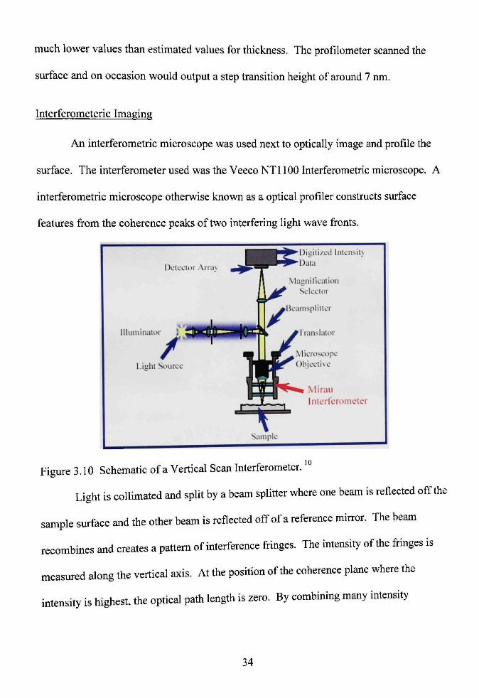
3.10 Schematic of a Vertical Scan Interferometer.'° 34
VI

3.11 Interferometric Measurements 35
3.12 Barrier oxide - Al Interface After Anodization 36
3.13 SEM Image of Al - Barrier Oxide Interface 36
3.14 SEM Image - 20 V Sample 37
3.15 SEM Image - 25 V Sample 38
3.16 SEM Image - 30 V Sample 38
3.17 SEM Image 35 V Sample 39
3.18 SEM Image - 40 V Sample 39
3.19 SEM image - 45 V Sample 40
3.20 Anodization Oxide Growth Rate 41
3.21 Thickness Measurement Comparison 43
4.1 Picture of Measurement Setup 45
4.2 Image of Probed Sample 46
4.3 LabVIEW GUI 47
4.4 I-V Characteristic Curve (oxide thickness - 30 nm) 48
4.5 Log plot of Current (30 nm) 49
4.6 I-V curves for devices of different areas (30 nm) 50
4.7 Current density versus voltage (30 nm) 51
4.8 Projected Current Values Using Measured Values (30 nm) 53
4.9 Projected current for 5 device areas (30 nm) 53
4.10 Band Structures of MIM Tunnel Junctions 54
4.11 Fowler-Nordheim Plot (30 nm) 56
4.12 Fowler-Nordheim Plot of Multiple Area Devices (30 nm) 57
Vll
4.13 I-V for devices of different TJ areas (15 nm) 58
4.14 Current density versus voltage (oxide thickness - 15 nm) 59
4.15 Projected current for 4 device areas (15 nm) 59
4.16 I-E curves for 15 and 30 rmi thick barrier oxides 60
4.17 AFM Profile of Barrier Oxide Surface (15nm) 61
4.18 Fowler-Nordheim Plot of Multiple Area Devices (15 nm) 62
Vll l
CHAPTER 1
INTRODUCTION AND BACKGROUND
Motivation
Currently there is growing interest in a phenomenon known as magnetoresistance
that is used in the development of a new type of non-volatile memory and also in new
read head technologies.
Magnetoresistance (MR) is the modulation of current through materials based on
the magnetic orientation of the materials. This was first demonstrated in a device
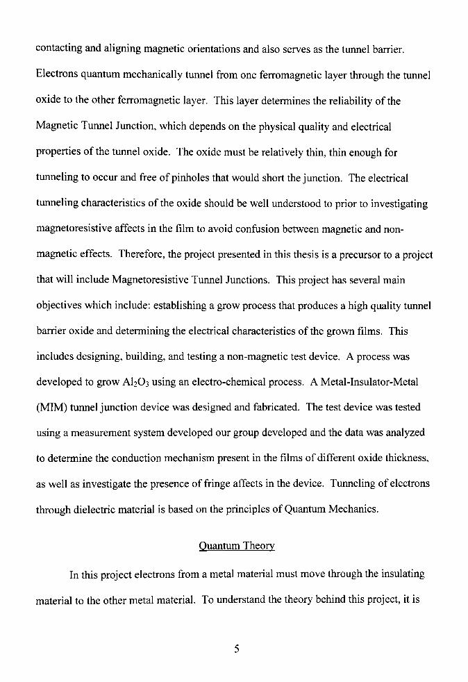
developed by IBM in the 1970s called a Magnetic Turmel Junction (MJT). An MJT is
multi-layer stack of magnetic and non-magnetic material. The figure below shows the
MJT device stack. It includes a 'free' ferromagnetic layer, a turmel barrier, a 'fixed'
ferromagnetic layer and a pinning anti-ferromagnetic layer.
. ^rromagnetic Layer M.OiBarri-
Fixed 1-erromagnetic Layer Pinnin" AF Layer
Figure 1.1 Magnetic Turmel Junction Layers
An anti-ferromagnetic layer with strong exchange coupling is used in contact with
the fixed layer, which pins the orientation of the layer in one direction (indicated by
arrows above). The orientation of the free ferromagnetic layer can be changed by an
applied magnetic field (indicated by arrows in figure above). The tunnel barrier used
between the layers is AI2O3.
The orientation of the free layer can be changed by an external magnetic field,
which changes the spin direction in the material. Electrons can only tunnel through the
barrier into an empty state with the spin direction.^ So, when the magnetic spin
orientations of the ferromagnetic layers are the same the tunneling current is high (low
MR) and when the layers have the opposite orientation the tunneling current is low (high
MR). The MR of the MTJ is defined as MR = - ^ ^^^. MTJs with this geometry are
reported as having MR values of 20-50%.'
Magnetoresistive Devices
Applications for this technology include magnetic read heads for high-density
hard disk drives, magnetic field sensors and magnetoresistive random access memory
(MRAM). Magnetic read heads and MRAM make use of the Magnetoresistive Tuimel
Jimction multi-layer device.
Magnetic Readheads
Read head devices for hard disk drives have adopted this technology to increase
the areal density and thus the bit density on the hard disk. Hard disk bits are laid out in a
linear configuration in rings or tracks around the disk. A single bit is a block of magnetic
material with a magnetic orientation. The orientation determines the state of the bit. The
figure below is a representation of the write/read configuration of the hard disk.^

MR sensor
1 Shield
Read head (MR)
^W Track t' width
/ Transition Magnetization
Magnetic recording medium
Figure 1.2 Magnetic Recording Process
The resistance of the magnetic tunnel junction changes as the magnetic read head
passes over the bit. The orientation of the free layer within the timnel junction is aligned
to the orientation of the bit, thus changing the resistance of the MJT. The development of
magnetic read heads has made it possible to increase the linear and track densities on the
hard disks making high-density hard disk drives possible.
Magnetic Random Access Memory
MRAM is similar to hard disks in that data is stored in magnetic cells. The state
of the cell is changed by magnetic field applied by current flowing near the cell in bit and
word lines. Both bit and word lines must be active to produce a saturating field large
enough to change the state of the free magnetic layer in the Magnetic Tuimel Junction.
The state is determined by flowing a small current through the MJT to determine the
resistance of the jimction. The configuration of the memory is shown in the figure below
from the IBM research website.
Reading a bit
bit line
word line
Writing 1 Writing O'
wordhrte
Figure 1.3 MRAM Structure
Magnetic Random Access Memory (MRAM) is currently in development using
this same technology. MRAM has many advantages over conventional memory devices.
MRAM has proven to be 6 times faster than DRAM (dynamic) that requires a constant
refresh and as fast as SRAM. MRAM can also be significantly more dense than SRAM.
The main advantage MRAM is its non-volatile nature. It retains data when the power is
removed. The implementation of this technology could make computers faster, reduce
power consumption and also eliminate the boot-up process by retaining the memory
states after turn-off. MRAM is also faster and less expensive than present non-volatile
Flash memory.
Relation of Magnetoresistance to MIM TJ
A Magnetic Tuimel Junction relies on the change in the magnetic orientation of
the ferromagnetic layers, which in turn changes the resistance of the junction. The
jimction also relies on a process known as tunneling. The layer between the magnetic
layers is an insulator and that prevents the two magnetic materials from physically
contacting and aligning magnetic orientations and also serves as the tunnel barrier.
Electrons quantum mechanically tunnel from one ferromagnetic layer through the tunnel
oxide to the other ferromagnetic layer. This layer determines the reliability of the
Magnetic Tuimel Junction, which depends on the physical quality and electrical
properties of the tunnel oxide. The oxide must be relatively thin, thin enough for
tunneling to occur and free of pinholes that would short the junction. The electrical
tunneling characteristics of the oxide should be well understood to prior to investigating
magnetoresistive affects in the film to avoid confusion between magnetic and non
magnetic effects. Therefore, the project presented in this thesis is a precursor to a project
that will include Magnetoresistive Tunnel Junctions. This project has several main
objectives which include: establishing a grow process that produces a high quality tunnel
barrier oxide and determining the electrical characteristics of the grown films. This
includes designing, building, and testing a non-magnetic test device. A process was
developed to grow AI2O3 using an electro-chemical process. A Metal-Insulator-Metal
(MIM) tunnel junction device was designed and fabricated. The test device was tested
using a measurement system developed our group developed and the data was analyzed
to determine the conduction mechanism present in the films of different oxide thickness,
as well as investigate the presence of fringe affects in the device. Tunneling of electrons
through dielectric material is based on the principles of Quantum Mechanics.
Quantum Theory
In this project electrons from a metal material must move through the insulating
material to the other metal material. To understand the theory behind this project, it is
important to understand how conduction occurs in insulating material. Conduction in
materials was first explained using classical physics and was later modified using
quantum physics. Conduction in metal is fairly simple and was described classically as
electrons moving through metal as a sea of free electrons and was later elaborated on
using quantum theory with the addition of the concept of quantized energy states.
Understanding the movement of electrons through an insulation material is vital to
understanding the theory behind this project. Conduction in insulators is not possible in
classical physics without the breakdown of the material. Quantum theory makes it
possible for electrons to appear on the other side of the insulator, otherwise knowTi as
tunneling through the insulating material. In order to understand this phenomenon, a
short introduction to quantum theory is required.
Quantum physics originated following the ultraviolet catastrophe. This
phenomenon describes the disagreement between the classical physics Rayleigh-Jeans
law describing blackbody radiation intensity versus wavelength and experimental data
taken of blackbody radiation. Following this in 1900, Max Planck developed an equation
that fully describes blackbody radiation. During this work he assumed that the oscillating
molecules have only discrete energy values equal to E^ = nhf, where n is a positive
integer known as the quantum number, h is Planck's constant, and/is the natural
frequency of the molecule oscillation. Every energy level is considered the quantum
state. He also proposed that when a molecule moves from one energy level to another,
the molecule emits or absorbs a photon of energy,
E„=hf. (1-1)

Planck's concept of quantized energy was revolutionary to physics and later research
based on this concept was used to explain physical phenomenon that could not be
explained by classical physics."*
In 1921 Einstein extended quantization to describe the photoelectric effect, were
he suggested that light waves were made up of photons. This concept was also used by
Niels Bohr to model the atom. The Bohr model states the electrons occupy discrete orbits
around the atom nucleus. This is very different from the classical model of the atom that
says that the electrons constantly give off radiation and eventually spiral into the nucleus
of the atom. In the quantum model radiation is only given off when an electron moves to
a lower energy state. The change in energy of the electron is equal to h*f.
From this concepts Louis de Broglie suggested that since photons have particle
and wave properties that maybe all forms of matter have both properties. During de
Broglie's Nobel Prize acceptance speech he suggested that electrons must also have wave
properties. To investigate this assertion, the double slit experiment was applied for
electrons. This experiment showed that electrons do if fact exhibit wave like properties.
Wave properties of matter
The results of the double-slit experiment show unmistakable evidence of the wave
property of electrons. An interference pattern is produced on the other side of the sUts. If
the electrons only had particle properties the pattern would just be the addition of the
distribution fi-om the individual slits.
The wave property of matter is described by a complex-valued wave function, \}/.
The wave function gives all of the information that can be known about the particle. The

absolute square, | |% of the wave function describes the probability of finding a particle
at a given point and time. The wave equation for a free particle moving along the x-axis
can be written as,
i/{x)=Asm\-^\ = Asm{kx) (1.2)
and the probability density, the probability per unit volume is | y/(x) p.^
For every system there are boundary conditions that exist for the system that
defines a set of wave functions. Each wave function describes the wave properties for a
particle with a given energy. These wave functions must also satisfy the Schrodinger
equation. One method in quantum mechanics is to obtain a solution to the equation,
which will give the allowed wave functions and energy states of the system."*
The Schrodinger equation for a particle moving along the x-axis that is
independent of time is
-^^--(E-U),. 0.3)
Equation 1.3 can be solved and the allowed wave functions for the system can be
determined if the value of the potential energy U(x) at the boundaries of the system are
known. Wave functions from one boundary to the next must be continuous. This is the
most important concept for the concept of electrons tunneling through a potential barrier.''
The figure below illustrates the barrier penetration situation. The wave function
in the region of the barrier exponentially decays and if the barrier is sufficiently thin so
that the wave function does not decay to zero then the wave fimction will continue on the
other side of the barrier with smaller amplitude.

Barrier V/( V) = A,e~'"J
Amplitude A,^
•- Tunnelinu
Figure 1.4 Barrier Penetration^
This means that there is finite probability that an electron that hits this barrier can be
found on the other side of the barrier. Contrary to classical physics that states, when a
particle hits this energy barrier the particle would be reflected and could not cross
through the barrier.
The probability that electrons will turmel through the barrier is exponentially
dependent on the barrier height and thickness. There are several different types of
tunneling that is discussed fiirther in Chapter 4. Experimental data obtained from the
MIM Tunnel Junctions leads to Fowler-Nordheim tunneling as the conduction
mechanism in the films. The MIM TJ device description and fabrication process is
described in the following chapter.
CHAPTER 2
NON-MAGNETIC TUNNEL JUNCTION DEVICE DESIGN
A Metal-Insulator-Metal (MIM) tunnel junction was developed to determine the
physical and electrical properties of a barrier oxide, AI2O3. In this chapter, a description
of the device function and the physical design will be discussed. The fabrication process
will also be described. This includes, mask design and layout, thermal oxidation,
lithography, metal deposition and anodization.
MIM Tunnel Junction Function
The fimction of the MIM tunnel junction is to allow the characterization of the
AI2O3 film in a simple device structure. A tunnel junction is a device made up of a three
fimctional layers: metal layer 1, dielectric material (in this case AI2O3), and metal layer 2.
An electric field created in the oxide by a voltage is applied across the two electrodes.
When this field approaches the breakdown field of the oxide quantum mechanical
tunneling as described in detail in Section 1.3.3, will begin. The tunneling current from
this device will be measured and characterized and the conclusions taken from this
project will be used in a subsequent project that uses AI2O3 in a magnetoresistive tunnel
junction for the use in Magnetic read head or MRAM applications.
MIM Tunnel Junction Structure
As stated above the tunnel junction is made up of three layers, the bottom
electrode is a 75 nm thick Al, the dielectric material AI2O3 with a specified thickness, and
the top electrode is a 75 nm Al layer. The TJ is fabricated on a Si wafer substrate with a
10
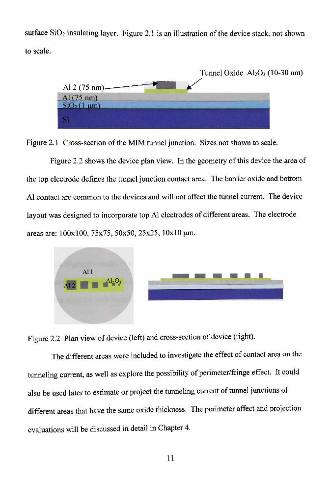
surface Si02 insulating layer. Figure 2.1 is an illustration of the device stack, not shovm
to scale.
Tunnel Oxide AI2O3 (10-30 nm)
Al 2 (75 nm). ^
Al (75 nm;>
Figure 2.1 Cross-section of the MIM tunnel junction. Sizes not shown to scale.
Figure 2.2 shows the device plan view. In the geometry of this device the area of
the top electrode defines the tunnel junction contact area. The barrier oxide and bottom
Al contact are common to the devices and will not affect the tunnel current. The device
layout was designed to incorporate top Al electrodes of different areas. The electrode
areas are: 100x100, 75x75, 50x50, 25x25, 10x10 ^m.
Figure 2.2 Plan view of device (left) and cross-section of device (right).
The different areas were included to investigate the effect of contact area on the
ttinneling current, as well as explore the possibility of perimeter/fringe effect. It could
also be used later to estimate or project the tunneling current of ttinnel junctions of
different areas that have the same oxide thickness. The perimeter affect and projection
evaluations will be discussed in detail in Chapter 4.
11
Device Layout and Fabrication
The fabrication of the MIM Tunnel Junction uses standard semiconductor
processes on 2" Si wafers. A 2" wafer will contain a 25x25 array of the set of 6 devices
shown in the plan view of Figure 2.2. This 2" wafer contains 3,750 individual tunnel
junctions with the same oxide thickness. There are five main process steps (1) fabrication
process design, (2) thermal oxidation, (3) bottom contact deposition, (4) oxide patterning
and growth, and (5) top contact lift-off.
Fabrication Process Design
The first step in the fabrication of the device is determining the process flow. It
requires some design thought. Each of the processes must work in harmony with the
others and the design of the device must include features not only necessary for device
function, such as known tunnel junction contact areas, but also for fabrication like
photomask alignment marks or considering features necessary for a later process. The
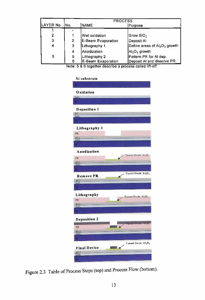
process steps are determined and checked for compatibility. Figure 2.3 below describes
the process steps for each layer in the device.
12
LAYER No.
T- C
M
3 4
5
No.
1 2 3
4 5 6
PROCESS NAME Purpose
Wet oxidation E-Beam Evaporation Lithography 1
Anodization Lithography 2 E-Beam Evaporation
Grow Si02 Deposit Al Define areas of AI2O3 growth
AI2O3 growth Pattern PR for Al dep. Deposit Al and dissolve PR
Note: 5 & 6 together describe a process called lift-off
Si substrate
Oxidation
Deposition 1
Lithography 1 PR
-AJJ
Anodization
PR
Al 1
^ Tunnel Oxide AI2O3
Remove PR ^ Tunnel Oxide AI2O3
Lithography PR
A l l
Tunnel Oxide A1,0,
Figure 2.3 Table of Process Steps (top) and Process Flow (bottom).
13
Now that the processes are knovra for each device layer, the lithography
photomask must be designed and created for the two lithography steps in the process
flow.
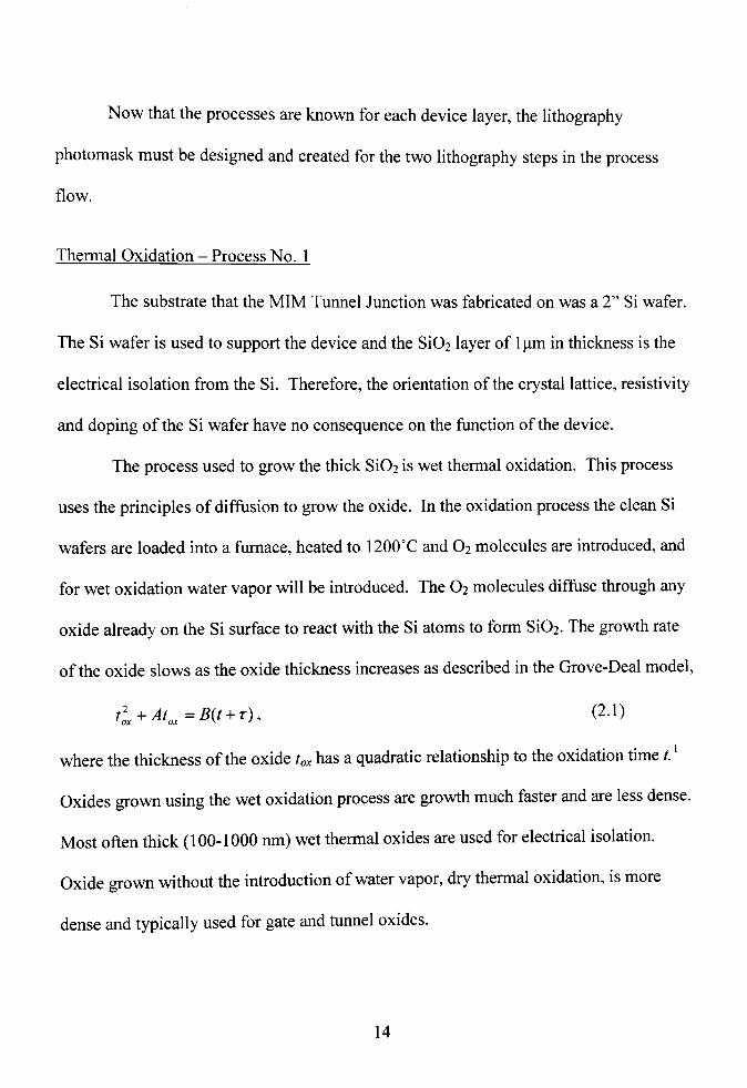
Thermal Oxidation - Process No. 1
The substrate that the MIM Tunnel Junction was fabricated on was a 2" Si wafer.
The Si wafer is used to support the device and the Si02 layer of 1 [xm in thickness is the
electrical isolation from the Si. Therefore, the orientation of the crystal lattice, resistivity
and doping of the Si wafer have no consequence on the function of the device.
The process used to grow the thick Si02 is wet thermal oxidation. This process
uses the principles of diffusion to grow the oxide. In the oxidation process the clean Si
wafers are loaded into a furnace, heated to 1200°C and O2 molecules are introduced, and
for wet oxidation water vapor will be introduced. The O2 molecules diffuse through any
oxide already on the Si surface to react with the Si atoms to form Si02. The growth rate
of the oxide slows as the oxide thickness increases as described in the Grove-Deal model,
ti+At„,=B(t + r), (2.1)
where the thickness of the oxide U has a quadratic relationship to the oxidation time t.
Oxides grown using the wet oxidation process are growth much faster and are less dense.
Most often thick (100-1000 nm) wet thermal oxides are used for electrical isolation.
Oxide grown without the introduction of water vapor, dry thermal oxidation, is more
dense and typically used for gate and tunnel oxides.
14

The oxidation process used for this device is outlined below and can be seen in
more detail in the appendix under process checklists.
1. Load Si wafers
2. Turn-on furnace and water hot plate
3. Adjust final temperature to 1100°C
4. Turn on O2 feed at 600°C
5. Begin timing at 1100°C for 1 hr
6. Turn off furnace
7. Turn off02 feed at 600°C
8. Cool dowTi to room temperature
9. Unload wafers
A Scanning Electron Microscope (SEM) image of the Si substrate and Si02 layer is
shown below.
Si02 {
lum EHT=17 00kV
I I W0= 3
Sign«l A " InLons Date 4 May 2004
Pho toNo= ie44 Time 11:04 00
Figure 2.4 SEM Image of Si02
15

The next step in the fabrication process is the deposition of the bottom Al contact,
layer 3 in Figure 2.3. In the anodization process it is necessary to make electrical contact
to the entire wafer surface. Therefore the bottom contact will be a "blanket deposition of
Al, meaning that the entire wafer surface will coated with Al. The process used to
deposh the Al metal layer is Electron-Beam (E-Beam) Evaporation.
E-Beam Evaporation - Process No. 2
E-Beam Evaporation is a process used to deposit metal and sometimes insulators
onto wafer samples. The system is comprised of a vacuum chamber, an evacuation
system, and a control system. The sample and target metal are held at a moderately high
vacuum (8x10' Torr) in the vacuum chamber. The chamber uses a two-stage evacuation
procedure where a roughing pump will bring the chamber to low vacuum (3x10"^ Torr)
from atmosphere and then a Cryo pump is used to bring the chamber to a high vacuum
level at ~8xlO" Torr. The control system is used to control the material specific power
output program, deposition rate and film thickness. The power output program is
responsible for controlling the power output by adjusting the current supplied to a
tungsten filament. The electrons will boil off the filament and a focused electron beam is
guided by magnetic fields onto the target metal held in a graphite crucible. Once the
melting point is reached, the metal will evaporate and travel across the vacuum chamber
and accumulate on the wafer surface as well as on the walls of the chamber. When the
program is ran it automatic mode the power is adjusted so that the specified deposition
rate is maintained. The power will then ramp down to zero once the specified thickness
is reached.
16
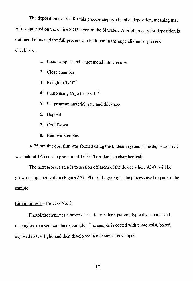
The deposition desired for this process step is a blanket deposition, meaning that
Al is deposited on the entire Si02 layer on the Si wafer. A brief process for deposition is
outlined below and the fiill process can be found in the appendix under process
checklists.
1. Load samples and target metal into chamber
2. Close chamber
3. Rough to 3x10"^
4. Pump using Cryo to ~8x 10'
5. Set program material, rate and thickness
6. Deposit
7. Cool Down
8. Remove Samples
A 75 nm thick Al film was formed using the E-Beam system. The deposition rate
was held at 1 A/sec at a pressure of 1x10" Torr due to a chamber leak.
The next process step is to section off areas of the device where AI2O3 will be
grown using anodization (Figure 2.3). Photolithography is the process used to pattern the
sample.
Lithography 1 - Process No. 3
Photolithography is a process used to transfer a pattern, typically squares and
rectangles, to a semiconductor sample. The sample is coated whh photoresist, baked,
exposed to UV light, and then developed in a chemical developer.
17
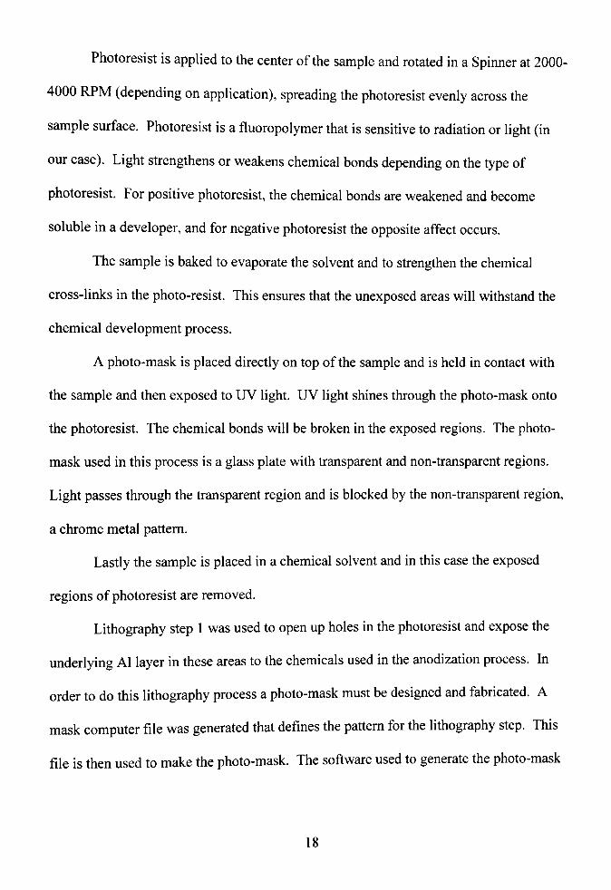
Photoresist is applied to the center of the sample and rotated in a Spinner at 2000-
4000 RPM (depending on application), spreading the photoresist evenly across the
sample surface. Photoresist is a fluoropolymer that is sensitive to radiation or light (in
our case). Light strengthens or weakens chemical bonds depending on the type of
photoresist. For positive photoresist, the chemical bonds are weakened and become
soluble in a developer, and for negative photoresist the opposite affect occurs.
The sample is baked to evaporate the solvent and to strengthen the chemical
cross-links in the photo-resist. This ensures that the unexposed areas will withstand the
chemical development process.
A photo-mask is placed directly on top of the sample and is held in contact with
the sample and then exposed to UV light. UV light shines through the photo-mask onto
the photoresist. The chemical bonds will be broken in the exposed regions. The photo
mask used in this process is a glass plate with transparent and non-transparent regions.
Light passes through the transparent region and is blocked by the non-transparent region,
a chrome metal pattern.
Lastly the sample is placed in a chemical solvent and in this case the exposed
regions of photoresist are removed.
Lithography step 1 was used to open up holes in the photoresist and expose the
underlying Al layer in these areas to the chemicals used in the anodization process. In
order to do this lithography process a photo-mask must be designed and fabricated. A
mask computer file was generated that defines the pattern for the lithography step. This
file is then used to make the photo-mask. The software used to generate the photo-mask
18

was LASI 7. Figure 2.5 below is (left) a view of one device rectangle and (right) a view
of the full wafer mask files.
ai">^- |«]»^. . - '«]f-Lui a — * " 0»Bi>M»'
Figure 2.5 Photo-mask for Lithography Step No. 1.
A mask file was also generated for the lithography step 2 in the same manner.
Lithography step no. 2 will be discussed later in the lift-off process section.
The lithography recipe used in this process is briefly outlined below. The
photoresist used was Shipley Microposit SI813 at an approximate thickness of 1 ^m and
the developer was MP Developer.
1. Spin on at 3700 RPM for 30 sec
2. Bakeat 115°Cfor 1 min
3. Exposure: Expose for 7 sec
4. Develop: 24 sec
5. Rinse: DIH2O
6. Hardbake: Bake at 120°C for 20 min
The next process step is to grow the AI2O3 oxide in the regions of the Al not covered by
photoresist (Figure 2.3).
19
Anodization - Process No. 4
The anodization process is the key process in the fabrication of the tunnel junction
device. The oxide layer is the focus of the project and the method by which the oxide is
grow will affect the function of the device. Anodization can produce the high quality
barrier oxide needed for this project. The anodization process was developed in the
Maddox lab as a crucial part of this project.
The following chapter will describe this process in detail as well as the
characterization of the anodic oxide films. Followdng the growth of the anodic tunnel
oxide as described in chapter 3, the photoresist was removed and the next process was
started. The last layer of the device, the top electrode, was fabricated in two process
steps (processes 5 and 6, Figure 2.3) called lift-off.
Lift-off- Process No. 5 and 6
This two-step process combines a lithography step and a deposition step. The end
result is a patterned metal layer. Photoresist is patterned on the sample and then Al is
deposited on the wafer. The Al will deposit on top of photoresist and on the oxide area
where the photoresist was removed. After the deposition the photoresist is dissolved in
acetone, leaving the Al deposited on the oxide surface and removing the Al on top of the
resist, thus called lift-off. Below is an illustration of the two steps to lift-off.
20

Pattern PR PR
- A U s^
Tunnel Oxide AljO^
Deposit All
Tunnel Oxide AljOj
Figure 2.6 Lift-off Process Flow.
For this process it work correctly the Al on the photoresist and the oxide can't be
a continuous layer and Al can not have a good step coverage (no deposition on the
sidewalls of photoresist.) This should not occur using E-Beam evaporation to deposit the
Al layer.
Electron-beam evaporation produces a deposition with virtually no vertical
sidewall coverage. This can be a disadvantage when complete coverage of all features is
needed or it can be an advantage, as in our case of liftoff (discussed in a later section),
when no sidewall coverage is desired.
There are two main factors involved in this phenomenon. At high vacuum levels,
the evaporated atoms travel in a straight line from the crucible to the nearest surface
where the atoms condense on that surface. This is shown by the large mean free path of
approximately 64 m calculated from
1 A = - (2.2)
4*V2*;r* — *r^ kT
21

Where r (1.82 A) is the mean radius of the atom, P (1x10'^ Torr) is the chamber pressure,
k is Bohzmann's constant and T (373 K) is the temperature. This means that the atoms
vsdll on average travel 65 m before the atoms collide and change direction. So, there
should be no atoms moving in arbitrary directions that may eventually land on the
vertical sidewalls of the wafer features.
Also the evaporated atoms diverge from the crucible in a 180° steradians cone, but
the largest angle of the incident atoms is 6 ° from the vertical axis. So, at this angle very
few atoms with hit the vertical sidewalls.
These factors help the process of lift-off where it is key that no metal is present on
the Photoresist sidewalls. Also, the lithography process used eliminates the hardbake
step at the end, which leads to rounded photoresist edges. The resulting sharp angle of
the photoresist at the edge ensures discontinuous coverage.
The lithography process is the same (except the hardbake step is removed) and
deposition is also the same process as described earlier. The mask files for lithography
set 2 are shown below where (left) is a view of one device rectangle and (right) is a view
of the full wafer design.
Figure 2.7 Photo-mask for Lithography No. 2.
22
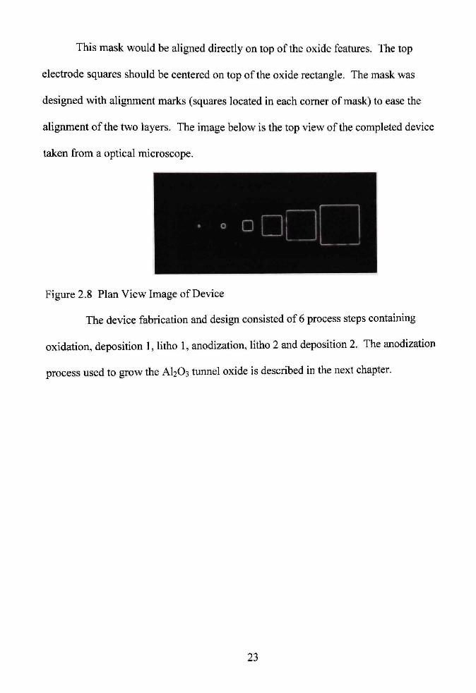
This mask would be aligned directly on top of the oxide features. The top
electrode squares should be centered on top of the oxide rectangle. The mask was
designed with alignment marks (squares located in each comer of mask) to ease the
alignment of the two layers. The image below is the top view of the completed device
taken from a optical microscope.
Figure 2.8 Plan View Image of Device
The device fabrication and design consisted of 6 process steps containing
oxidation, deposition 1, litho 1, anodization, litho 2 and deposition 2. The anodization
process used to grow the AI2O3 tunnel oxide is described in the next chapter.
23
CHAPTER 3
ANODIZATION OF ALUMINUM
Anodization is an electro-chemical process that produces an AI2O3 (oxide layer)
when Aluminum atoms react with oxygen atoms in an electrolytic solution in the
presence of an electric field.
Anodic oxide has two characteristic structures, porous oxide and non-porous
barrier-type oxide. A porous Al oxide is grown in an acidic electrolyte solution such as
sulfuric acid. Barrier-type oxides are grown in neutral electrolytic solutions such as
ammonium phosphate, borate and tartrate. Porous Al oxide is produced by a growth and
etch process that produces an ordered array of pores in the oxide layer. This oxide is a
thick oxide (up to 100 |im) and is often used as a protective coating on machined Al
parts. The barrier oxide is strictly a growth process and has electrical properties suitable
to be used as the dielectrics in capacitors.^ It contains no pores and is usually at least 100
times thinner than porous oxide.
Depending on the growth conditions, barrier oxides can be amorphous or
crystalline. The anodization procedure will be different depending on the desired
structure of the oxide, amorphous or crystalline. By changing the structure of the native
oxide present on the sample, the structure of the grown film will be changed. To produce
a crystalline oxide film the sample is annealed prior to anodization.
For crystalline oxide films an initial bake at ~550°C prior to anodization is added
to the procedure above. This bake produces a slightly thicker native oxide that contains
seed crystals for which the barrier oxide will grow. The field that the oxide supports is
higher for crystalline films. Thus, a higher voltage must be applied to begin conduction
24
and for the use as a tunnel junction eventually containing magneto resistive layer this
characteristic would lead to higher film resistivity and thus lower signal levels. For an
application that requires a crystalline film fiarther research is necessary to determine the
anodization growth characteristics of the appropriate current density and the approximate
voltage/thickness. For this project the aluminum oxide film will have an amorphous
structure.
Chemical Reaction
In anodization the sample is placed in an electrolytic solution, ammonium
pentaborate in H2O (borate-H20). The sample is coimected to the positive terminal, the
anode, of a power supply; a non-reactive metal plate is cormected to the negative
terminal, the cathode. An electric field is produced across the anode and cathode by an
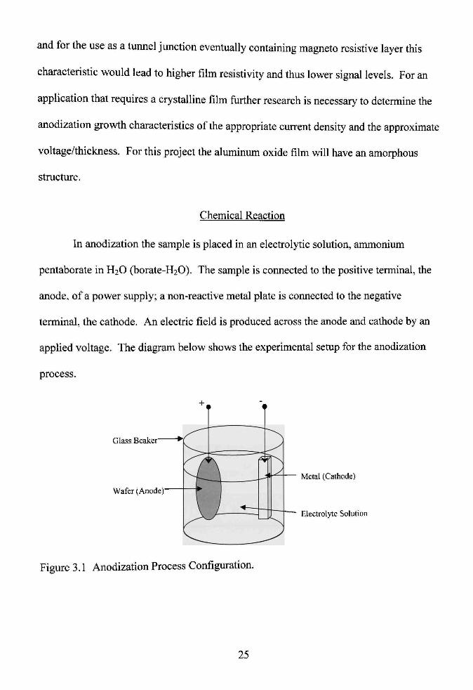
applied voltage. The diagram below shows the experimental setup for the anodization
process.
Glass Beaker •
Wafer (Anode)
Metal (Cathode)
Electrolyte Solution
Figure 3.1 Anodization Process Configuration.
25
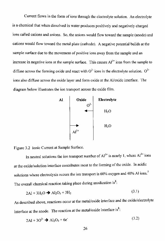
Current flows in the form of ions through the electrolyte solution. An electrolyte
is a chemical that when dissolved in water produces positively and negatively charged
ions called cations and anions. So, the anions would flow toward the sample (anode) and
cations would flow toward the metal plate (cathode). A negative potential builds at the
sample surface due to the movement of positive ions away from the sample and an
increase in negative ions at the sample surface. This causes Al ^ ions from the sample to
diffuse across the forming oxide and react with 0~" ions in the electrolyte solution. O '
ions also diffuse across the oxide layer and form oxide at the Al/oxide interface. The
diagram below illustrates the ion transport across the oxide film.
Al Oxide O 2-
Al 3+
Electrolyte
H2O
H2O
i3+ •
Figure 3.2 Ionic Current at Sample Surface.
In neutral solutions the ion transport number of Al "" is nearly 1, where Al^" ions
at the oxide/solution interface contributes most to the forming of the oxide. In acidic
solutions where electrolysis occurs the ion transport is 60% oxygen and 40% Al ions.^
The overall chemical reaction taking place during anodization is :
2A1 + 3H2O •» AI2O3 + 3H2 (3.1)
As described above, reactions occur at the metal/oxide interface and the oxide/electrolyte
interface at the anode. The reaction at the metal/oxide interface is^
2A1 + 30^' •» AI2O3 + 6e- (^-2)
26
The reaction at the oxide/electrolyte interface is^
2A13V 3H2O ^ AI2O3 + 6H^ (3.3)
The overall reaction in the solution produces a hydrogen gas evolution^:
6H^+6e"-*3H2 (3.4)
The composition of A1203 is 62% Al atoms and 38% oxygen atoms.
Anodization Procedure
During the process both the constant source current and the voltage are monitored
using a Keithley 2400 Source/meter that is interfaced and controlled using its GPIB
capabilities in conjunction with LabVIEW computer software. The current density used
during the process will affect the rate at which the oxide grows. The thickness of the
oxide is directly proportional to the final voltage level reached. Growth of the Al film
begins to occur around 1-2 V due to the native oxide present on the surface. As the
voltage is increased beyond this the thickness of the oxide is increased and E-field in the
oxide remains constant. When the voltage is kept constant the ionic current stops due to
a loss of potential difference. One advantage to this process is the ability to control the
thickness of the oxide by the voltage. The adjustment of the final voltage will determine
the final thickness of the oxide.
The procedure for growing amorphous aluminum oxide is outlined below:
1. Connect sample (anode) and metal (cathode) to power supply with clips
2. Place in electrolyte solution - 0.1 M ammonium pentaborate (borate-H20)
3. Anodize at constant current density of 1 mA/cm^ to the desired final voltage
4. Remain at final voltage for 60 sec.
27
Barrier Aluminum Oxide Characteristics
Barrier-type oxide grown on aluminum in a neutral electrolyte solution should not
contain pores and should be uniform in thickness due to the uniform voltage drop across
the sample surface. The oxide should have a density close to 3.17 g/cm^ and a refractive
index n = 1.767-1.772.^
The film needs to be uniform and free of pinholes. Pinholes are areas where the
film thickness is zero and the top and bottom aluminum electrodes are in direct contact.
The presence of pinholes would short the device and any tunneling current present would
be to weak to detect in comparison to the direct conduction. The thickness uniformity
could also affect the tuimeling current due to varying dielectric thickness. The uniformity
of the film was investigated in SEM micrographs and the presence of pinholes will be
evident in the I-V characteristics.
Film Growth Experiment
To determine the proper procedure for anodic oxide growth the following
experiment was performed. Test films were grown on aluminum and the film
characteristics and growth characteristics will be discussed.
A 1000 A Al layer was deposited by E-Beam Deposition onto a Si wafer substrate
and Positive Shipley SI813 photoresist was patterned using the standard
photolithography on the Al layer (masking some Al and exposing others to film growth).
This procedure was followed by a 20-minute hard bake at 120 °C.
28
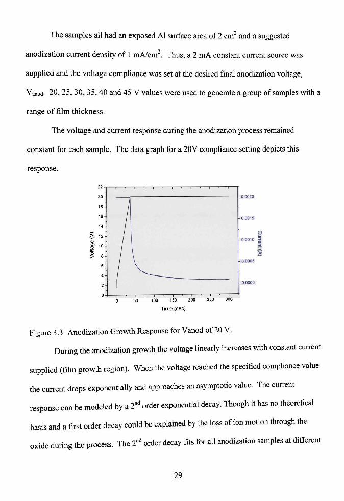
The samples all had an exposed Al surface area of 2 cm^ and a suggested
anodization current density of 1 mA/cm^. Thus, a 2 mA constant current source was
supplied and the voltage compliance was set at the desired final anodization voltage,
Vanod- 20, 25, 30, 35, 40 and 45 V values were used to generate a group of samples with a
range of film thickness.
The voltage and current response during the anodization process remained
constant for each sample. The data graph for a 20V compliance setting depicts this
response.
~\ 2 0 -
1 8 -
1 6 -
1 4 -
Vol
tage
(V
)
.1
.1
.1
..
6 -
4 -
2 -
0 -
1 1 1 ' 1 1
~1 / /
/
/ \
I ^^
1 ' 1 ' 1 1
- 0 0020
-0.0015
-00010
- 0 0005
- 0 0000
1 1 1 1 1 r 1 • 1 • 1 1 0 50 too 150 200 2SU JUU
Time (sec)
Figure 3.3 Anodization Growth Response for Vanod of 20 V.
During the anodization growth the voltage lineariy increases with constant current
supplied (film growth region). When the voltage reached the specified compliance value
the current drops exponentially and approaches an asymptotic value. The current
response can be modeled by a 2"" order exponential decay. Though it has no theoretical
basis and a first order decay could be explained by the loss of ion motion through the
oxide during the process. The 2"'' order decay fits for all anodization samples at different
29
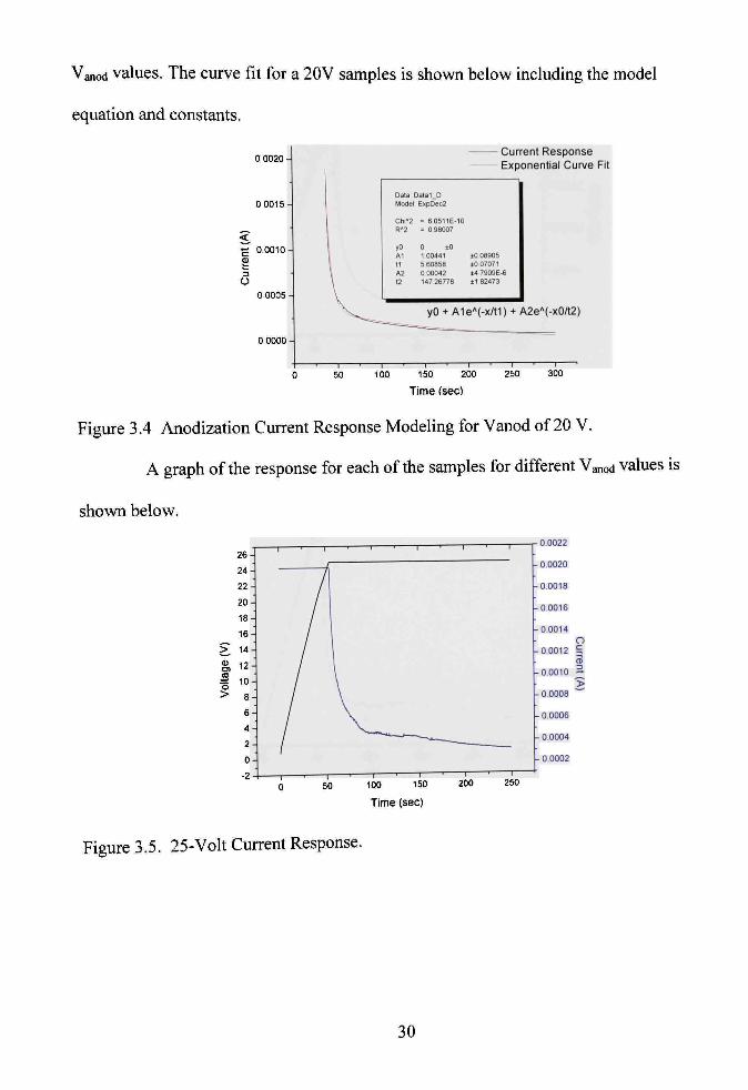
Vanod values. The curve fit for a 20V samples is shown below including the model
equation and constants.
0 0020
< ^ 0,0010-(U
fc o
0 0005
0 0000
Current Response Exponential Curve Fit
Data Model
Chl"2 R'2
yO Al t1 A2 12
3ata1 0 ExpDec2
= 60511E-10 = 0 98007
0 to 1 00441 5 60658 0 00042 147 26776
±0 08905 10 07071 t4 7909E.6 ±1 82473
yO + A1e''(-x/t1) + A2e"(-x0/t2)
100 — I —
150 200 250
Time (sec)
Figure 3.4 Anodization Current Response Modeling for Vanod of 20 V.
A graph of the response for each of the samples for different Vanod values is
shown below.
26-
24
22-
20-
18
16
14
12
10
8
6
4
2
0-
-2
0.0022
- 0.0020
-0.0018
0.0016
00014
O 0 0012 5
B 00010 3-
>
0.0008
0.0006
. 0.0004
- 0 0002
50 -T
150 100
Time (sec)
200
Figure 3.5. 25-Voh Current Response.
30

32
30
28
26-
24-
22-
20
18-1 0)
^ 16
o >
14
12-
10-
8
6
4
50 —r-100 150
Time (sec)
— I — 200 250
0 0005
0.0004
-0.0003
-0 0002 X >
0.0001
00000
Figure 3.6 30-Volt Current Response.
0)
•5 >
00022
- 0 0020
0.0018
00016
00014
o 0.0012 ^
00010 ^
> 00008
0.0006
0 0004
00002
100 150
Time (sec)
Figure 3.7 35-Voh Current Response.
31
4 0 -
30
(U 20
ss >
/
/
• /
/
; /
' 1 1 ' 1 -• 1 ' 1
1 ' 1 • i ' 1 ' 1 1 1 ' — 1 — 1
0 5 0 100 150 200 250 300
- 0 0 0 2 0
-0 0015
o c —t
-00010 s (A)
-0.0005
-0 0000
Figure 3.8 40-Vok Current Response. Time (sec)
50
40
30-
S" 20 o >
10
1 ' 1 ' 1 ' 1 1 1 1 1 1 r
— I 1 1 • 1 1 1 ' 1 ' 1 — 50 100 150 200 250 300
Time (sec)
00020
0.0015
-0.0010 o c
3
0.0005
-0.0000
Figure 3.9 45-Voh Current Response.
32
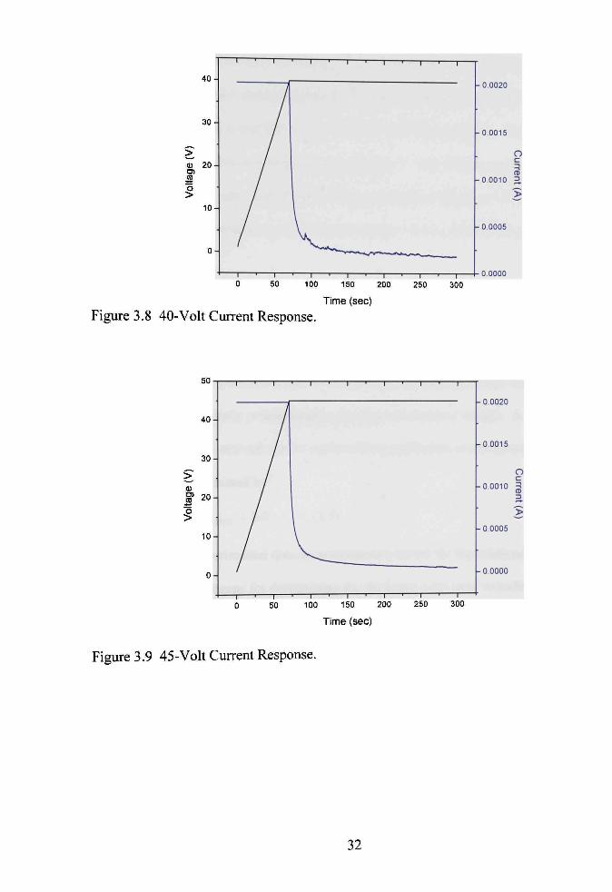
The response curves are very similar. It is evident from each that the voltage
increases and the current remains constant while the oxide is growing and when the
specified final voltage is reached the current decreases exponentially. Also, most of the
graphs show an increase in voltage at approximately 1 volt, which corresponds to a native
oxide thickness of ~1 nm. The 30 and 35 Volt anodization begins at ~4 volts because the
process was stopped with an oxide thickness around 5-6 nm and then the process was
restarted.
Film Thickness Determination
Determination of the thickness of the film is necessary to determination of the
relationship between final anodization voltage VANOD and the thickness. The thickness of
the anodic film is directly proportional to the final anodization voltage. A growth rate
ranging from 1.2-1.4 nm/volt can be expected for anodization of aluminum. ' The
thickness can be estimated by^,
c/ = 1.24xF^^o^+2.0. (3.5)
Through experimental data measurements a model for the relationship will be
presented. Several means for determining the thickness were used including profilometer
measurements, interferometric microscope measurements, SEM images and capacitance
measurements.
Profilometer Measurements
The first attempted method used the Dektak profilometer, which physically scans
the surface with a stylus. This method gave inconsistent resuhs for the thickness and
33
much lower values than estimated values for thickness. The profilometer scanned the
surface and on occasion would output a step transition height of around 7 nm.
Interferometeric Imaging
An interferometric microscope was used next to optically image and profile the
surface. The interferometer used was the Veeco NT 1100 Interferometric microscope. A
interferometric microscope otherwise known as a optical profiler constructs surface
features from the coherence peaks of two interfering light wave fronts.
DclccliM . \ l i a \
kiiiiiiialor
Diyili/Ld lnUii.sil>
)ala
Magnilkai iod Sclccior
Light Source
.Mi rail Interferometer
Sample
Figure 3.10 Schematic of a Vertical Scan Interferometer.
Light is coUimated and split by a beam splitter where one beam is reflected off the
sample surface and the other beam is reflected off of a reference mirror. The beam
recombines and creates a pattern of interference fringes. The intensity of the fringes is
measured along the vertical axis. At the position of the coherence plane where the
intensity is highest, the optical path length is zero. By combining many intensity
34

measurements the surface of the sample can be constructed by referencing the reference
10 mirror. The figure below shows the images captured using this method.
^Veeco X Profile X: 0J56 mm
Oft) q
OfiO -
OX' -
0 Ic -
i^V^^^^^^^
^wpl '
F
~ i — I — I — 1 — 1 — I — I — I — [ — r
00 01 o ; o j 01 05 0& o : 08 0^ 10 11 1.: u u
Y Profile X: 30 8 urn
fx. 542.9 Jtii ^ ( Y -3 6nm J
X Y Ht Dist
Angle
115 0.33
-2 69
- mm mm
- am - mm
"
Title: Subregion
Note: X offset: 16 " Y offset: 141
>00 TOO
Figure 3.11 Interferometric Measurements.
The vertical transition from Al to AI2O3 is shown at ~9nm and the thickness
estimated from equation 3.1 was 26.8 nm. A conclusion was taken from this
measurement and the previous measurements. During anodization the oxide consumes a
portion of the Al and grows not only up from the sample surface but down as well. The
illustration shows the cross-sectional profile of the grown oxide.
35
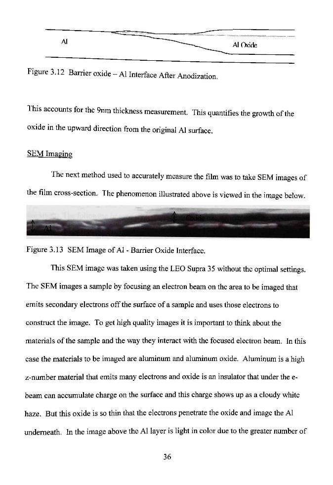
Al Oxide
Figure 3.12 Barrier oxide - Al Interface After Anodization.
This accounts for the 9nm thickness measurement. This quantifies the growth of the
oxide in the upward direction from the original Al surface.
SEM Imaging
The next method used to accurately measure the film was to take SEM images of
the film cross-section. The phenomenon illustrated above is viewed in the image below.
Figure 3.13 SEM Image of Al - Barrier Oxide Interface.
This SEM image was taken using the LEO Supra 35 without the optimal settings.
The SEM images a sample by focusing an electron beam on the area to be imaged that
emits secondary electrons off the surface of a sample and uses those electrons to
construct the image. To get high quality images it is important to think about the
materials of the sample and the way they interact with the focused electron beam. In this
case the materials to be imaged are aluminum and aluminum oxide. Aluminum is a high
z-number material that emits many electrons and oxide is an insulator that under the e-
beam can accumulate charge on the surface and this charge shows up as a cloudy white
haze. But this oxide is so thin that the electrons penetrate the oxide and image the Al
underneath. In the image above the Al layer is light in color due to the greater number of
36
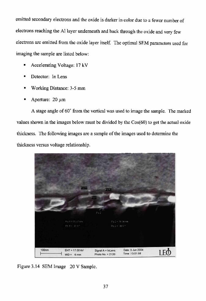
emitted secondary electrons and the oxide is darker in color due to a fewer number of
electrons reaching the Al layer underneath and back through the oxide and very few
electrons are emitted from the oxide layer itself. The optimal SEM parameters used for
imaging the sample are listed below:
• Accelerating Voltage: 17 kV
• Detector: In Lens
• Working Distance: 3-5 mm
• Aperture: 20 |j.m
A stage angle of 60° from the vertical was used to image the sample. The marked
values shown in the images below must be divided by the Cos(60) to get the actual oxide
thickness. The following images are a sample of the images used to determine the
thickness versus voltage relationship.
lOOnm EHT = 17.00 kV
I WD = 6 mm
Signal A = InLens
Photo No. = 2120
Date :3 Jun 2004 Time :1 3:01:68
Figure 3.14 SEM Image 20 V Sample.
37
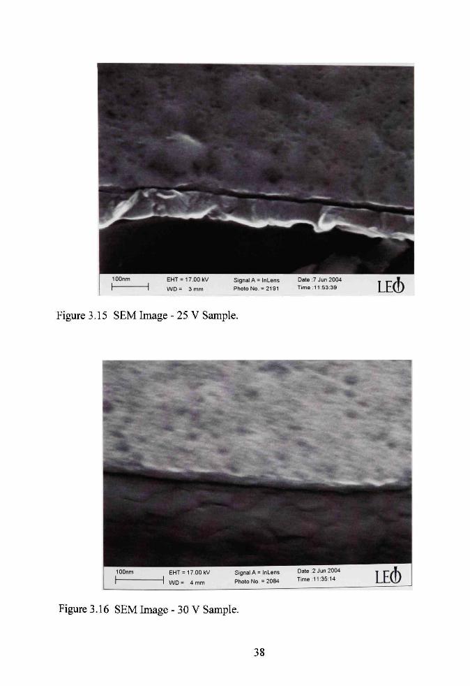
Figure 3.15 SEM Image - 25 V Sample.
Figure 3.16 SEM Image - 30 V Sample.
38
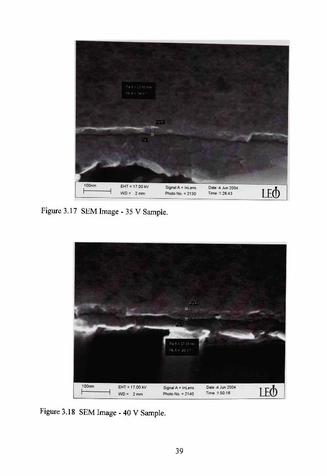
Figure 3.17 SEM Image - 35 V Sample.
Figure 3.18 SEM Image - 40 V Sample.
39
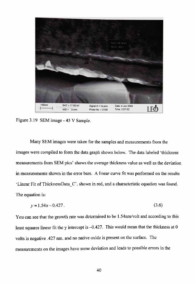
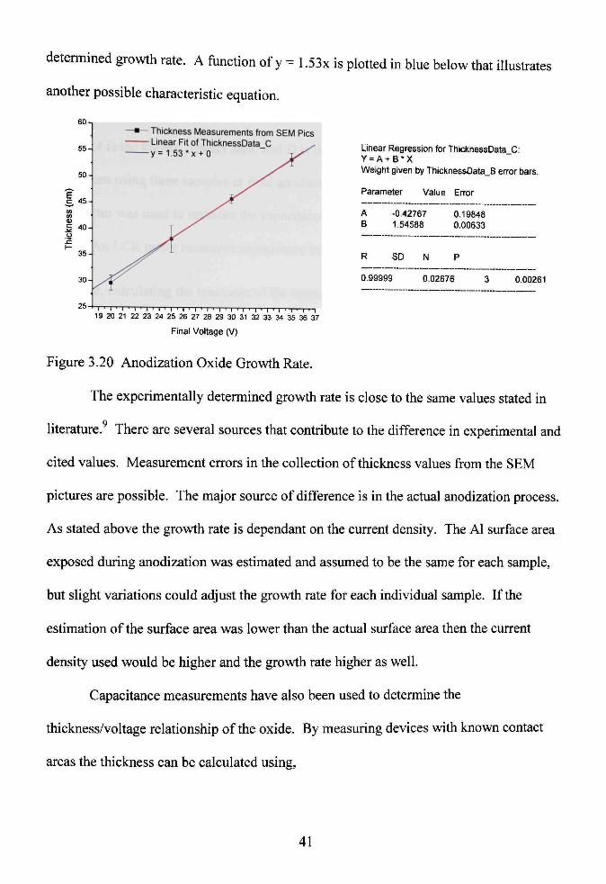
Figure 3.19 SEM image - 45 V Sample.
Many SEM images were taken for the samples and measurements from the
images were compiled to form the data graph shown below. The data labeled 'thickness
measurements from SEM pics' shows the average thickness value as well as the deviation
in measurements shown in the error bars. A linear curve fit was performed on the results
'Linear Fit of ThicknessDataC', showoi in red, and a characteristic equation was found.
The equation is:
:v = 1.54x-0.427. (3.6)
You can see that the growth rate was determined to be 1.54nm/volt and according to this
least squares linear fit the y intercept is -0.427. This would mean that the thickness at 0
vohs is negative .427 nm. and no native oxide is present on the surface. The
measurements on the images have some deviation and leads to possible errors in the
40
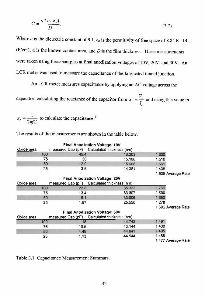
determined growth rate. A function of y = 1.53x is plotted in blue below that illustrates
another possible characteristic equation.
- Thickness Measurements from SEIVI Pics - Linear Fit of ThicknessData_C -y= 1.53*x + 0 Linear Regression for ThicknessData_C:
Y = A + B * X Weight given by ThicknessData_B error bars.
Parameter Value Error
-0.42767 1.54588
0.19848 0.00633
SD N
0.99999 0.02676 0.00261
I ' I ' ' ' I ' I ' I ' I ' I ' I ' I ' I ' I ' I ' I ' I ' I ' I ' I ' I 19 20 21 22 23 24 25 26 27 28 29 30 31 32 33 34 35 36 37
Final Voltage (V)
Figure 3.20 Anodization Oxide Growth Rate.
The experimentally determined growth rate is close to the same values stated in
literature.^ There are several sources that contribute to the difference in experimental and
cited values. Measurement errors in the collection of thickness values from the SEM
pictures are possible. The major source of difference is in the actual anodization process.
As stated above the growth rate is dependant on the current density. The Al surface area
exposed during anodization was estimated and assumed to be the same for each sample,
but slight variations could adjust the growth rate for each individual sample. If the
estimation of the surface area was lower than the actual surface area then the current
density used would be higher and the growth rate higher as well.
Capacitance measurements have also been used to determine the
thickness/voltage relationship of the oxide. By measuring devices with known contact
areas the thickness can be calculated using.
41
c = e*Sf^xA
D • (3.7)
Where e is the dielectric constant of 9.1, EQ is the permitivity of free space of 8.85 E -14
(F/cm), A is the known contact area, and D is the film thickness. These measurements
were taken using three samples at final anodization voltages of lOV, 20V, and 30V. An
LCR meter was used to measure the capacitance of the fabricated tunnel junction.
An LCR meter measures capacitance by applying an AC voltage across the
capacitor, calculating the reactance of the capacitor from x^. = ^ - and using this value in
1 x„ — ' InfC
to calculate the capacitance."
The results of the measurements are shown in the table below.
Final Anodization Voltage: 10V Oxide area measured Cap (pF) Calculated thickness (nm)
100 75 50 25
49.4 30
12.9 3.5
16.303 15.100 15.608 14.381
Table 3.1 Capacitance Measurement Summary.
1.630 1.510 1.561 1.438 1.535 Average Rate
Oxide area ^ ^ ^ ^ ^
^HP
Oxide area
^•B IHIIIh
100 75 50 25
100 75 50 25
Final Anodization Voltage: 20V measured Cap (pF) Calculated thickness (nm)
1 ^ ^ ^ ^ . 22.8 m«mmm«,«mmmi 35.322 13.4 33.807 6.1 - ' ^ ^ ^ ^ 33.006
1.97 25.550
Final Anodization Voltage: 30V measured Cap (pF) Calculated thickness (nm)
18 44.742 10.5 43.144
vtwrnmrne^-T^k 1.690 1.650 1.278 1.596/
^ ^ • 1 . 4 9 1 1.438
:^^^^^^: 4 . 4 y iip^a^H^flMi^itte»n«^w .noO
1.13 44.544 1.485 1.477 Average Rate
42
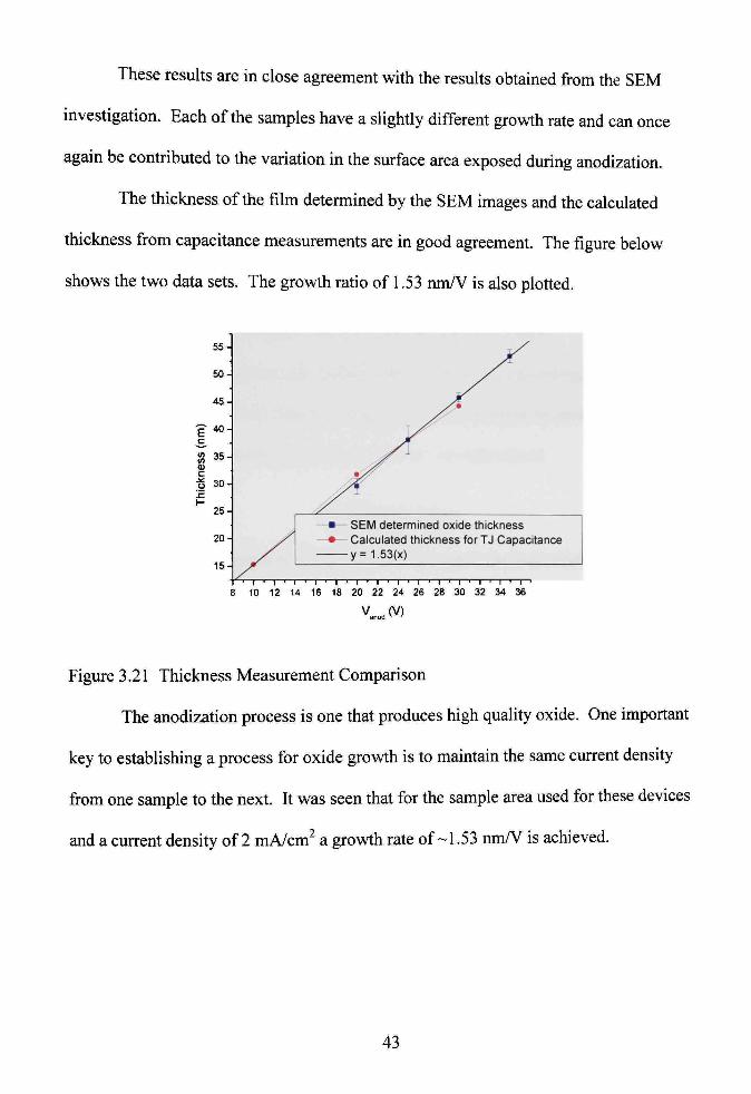
These results are in close agreement with the results obtained from the SEM
investigation. Each of the samples have a slightly different growth rate and can once
again be contributed to the variation in the surface area exposed during anodization.
The thickness of the film determined by the SEM images and the calculated
thickness from capacitance measurements are in good agreement. The figure below
shows the two data sets. The growth ratio of 1.53 nnW is also plotted.
55
50
4 5 -
4 0 -
35
30
25
20
15-
SEM determined oxide thickness Calculated thickness for TJ Capacitance
-y=1.53(x)
I ' I ' I ' I ' I ' I ' I ' I ' I ' I ' I ' I ' I ' I ' 8 10 12 14 16 18 20 22 24 26 28 30 32 34 36
anod ^ '
Figure 3.21 Thickness Measurement Comparison
The anodization process is one that produces high quality oxide. One important
key to establishing a process for oxide growth is to maintain the same current density
from one sample to the next. It was seen that for the sample area used for these devices
and a current density of 2 mA/cm^ a growth rate of-1.53 nnW is achieved.
43
CHAPTER4
ELECTRICAL CHARACTERIZATION AND EXPERIMENTS
As described in chapter 1, the tunnel oxide barrier in the MIM tunnel junctions
will be used in magnetoresistive devices containing ferromagnetic layers. It is beneficial
to determine the electrical characteristics of the tunnel oxide prior to developing a more
complex device. Knowing the tunneling characteristics of the nonmagnetic device will
help to separate magnetoresistive affects from non-magnetic affects.
This chapter describes the methods used to determine the electrical characteristics
for the MIM device. Using current-voltage plots, an area/perimeter analysis was
conducted and the dominant turmeling mechanism was determined.
Measurement Setup
The electrical characterization of the MIM tunnel junctions relies on the I-V
characteristics obtained during device testing. The system used to generate the I-V
incorporates three main devices, a probe station for electrical connection to the device
electrodes, a Keithley 2400 SourceMeter for power source and measure operations, and
computer software and computer to accurately control source and measure functions the
SourceMeter. A picture of the test setup is shown below.
44

Figure 4.1 Picture of Measurement Setup
Probe Station
The probe station is the blue instrument shown in the picture above. It includes
the probes / probe manipulators, microscope, sample stage. The probes serve as electrical
connections to the source meter. The probe tips are positioned over the MIM device
using the probe manipulators. The probes are then lowered onto the MIM electrodes.
The probe has a 5 ^m tip diameter that can probe the 100x100, 75x75, 50x50, 25x25, and
10x10 i m squares. The microscope is used to view the probing area. The stage is used
to access different areas on the sample surface. The picture below is an image of a device
that is being probed on the 100x100 |.im square.
45

Figure 4.2 Image of Probed Sample.
The probes are connected to the Keithley 2400 SourceMeter.
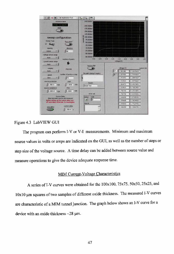
Keithley 2400 and LabVIEW
The SourceMeter is a device that combines the function of a multimeter and a
power supply. It is a highly precise device that accurately measures currents in the pico-
Amp range. NI LabVIEW software was developed to acquire data from the Keithley
2400 and to control a basic sweep function. The LabVIEW software uses a GPIB
interface to send commands to the Keithley. The program developed sends consecutive
voltage source then current measure commands to the SourceMeter to generate an 1-V
curve characteristic of the MIM device. The program controls a voltage step fimction
that is sent to the Keithley 2400 and the current is measured after each increase in the
voltage level. The program plots the I-V curve and produces an excel file containing the
I-V data. The image below is a screen capture of the graphical user interface of the
LabVIEW program used for I-V measurements.
46
• 11 13ptApphc4tKNiFont
rMoucsrwM
M l ^-IPS'
sweep configuration Siwplype fou.™.es'
drertion
nijmb«t of ponts
step see
mxnber of points or st«p
sprang
Unear v j vokage sense range
Auto T - |
current sense range
Auto t r |
langng
Auto
speed
Slow
•e j
v l '/ - l?5
start source protection
^l.OOe+0 V/A ijj-3.0000 V/A
souce compience stop
y|l.0OE+O V/A i l.OOOO V/A
Source Delay \ (tkne betiween source and measure) i before setting up the custorn delay turn
off auto deUy otherwise its mear«igless
autodeiay custorn delay
240.0000n-
lO .e iSOy-
-80.0000n =
•3 .0 -2 5 • : 0 - I
Bs
5 -1,0 -0.5 0.0 0.5 I
voltage (V) 0
T
Save to He?
itatui cod»
' ) " ^)|o
voltage (V)
• ; 081060
-;; 027030
-1 972970
-1 <11B920
-1.864870
-1 SI0810
-1 756760
-1 70Z700
-1,648650
-1 S94600
-1 540540
-1 486490
cw
|-:.164254E-5
|- l .7476S6£-S
|-1.389476£-5
|-1 0<*7<M6E-5
| -e 630156E-6
| -6 738r39E-6
| -5 2eSl68E-6
| -4 024092E-6
|-3,079853E-6
|-2,342445E-fc
| -1 77:^?7E-6
| - 1 334697E-6
Figure 4.3 LabVIEW GUI
The program can perform I-V or V-I measurements. Minimum and maximum
source values in volts or amps are indicated on the GUI, as well as the number of steps or
step size of the voltage source. A time delay can be added between source value and
measure operations to give the device adequate response time.
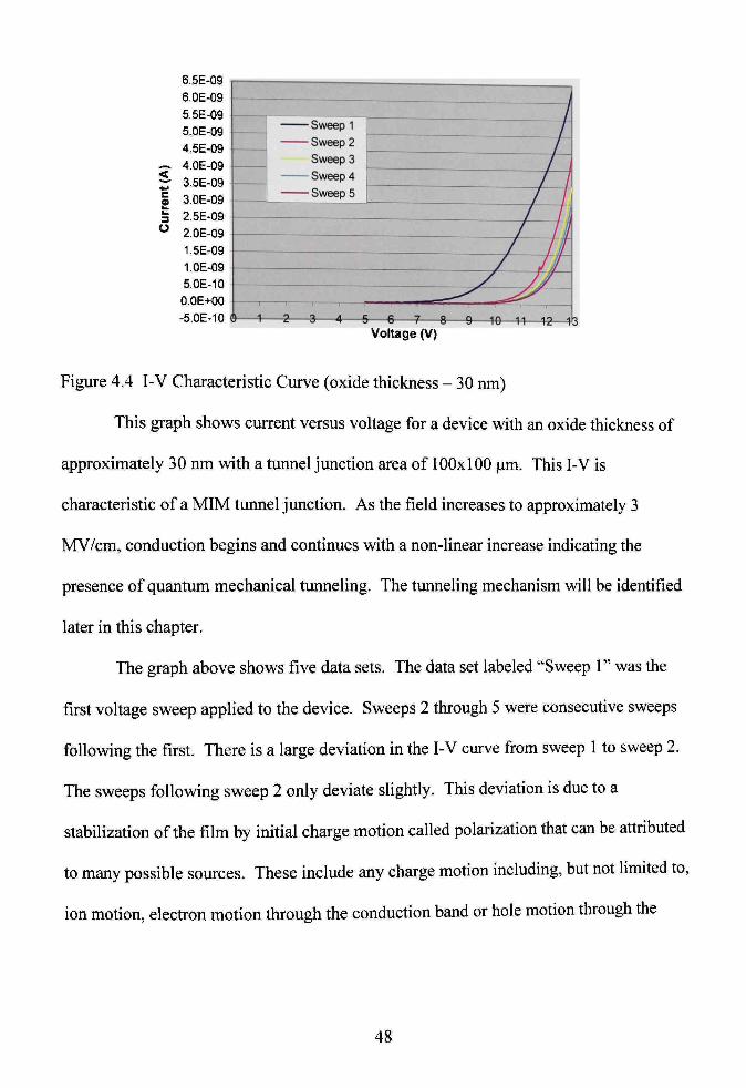
MIM Current-Voltage Characteristics
A series of I-V curves were obtained for the 100x100, 75x75, 50x50, 25x25, and
10x10 nm squares of two samples of different oxide thickness. The measured I-V curves
are characteristic of a MIM tunnel junction. The graph below shows an I-V curve for a
device with an oxide thickness -28 im.
47
6.5E-09 6.0E-09 5.5E-09 5.0E-09 4.5E-09
- - 4.0E-09 ~- 3.5E-09 I 3.0E-09 I 2.5E-09 " 2.0E-09
1.5E-09 1.0E-09 5.0E-10 O.OE+00 -5.0E-10 6 1 2 3 4 6- 6 7—8 9—«—«—43—lb
Voltage (V)
Figure 4.4 I-V Characteristic Curve (oxide thickness - 30 nm)
This graph shows current versus voltage for a device with an oxide thickness of
approximately 30 nm with a turmel junction area of 100x100 |j,m. This I-V is
characteristic of a MIM turmel junction. As the field increases to approximately 3
MV/cm, conduction begins and continues with a non-linear increase indicating the
presence of quantum mechanical tuimeling. The tunneling mechanism will be identified
later in this chapter.
The graph above shows five data sets. The data set labeled "Sweep 1" was the
first voltage sweep applied to the device. Sweeps 2 through 5 were consecutive sweeps
following the first. There is a large deviation in the I-V curve from sweep 1 to sweep 2.
The sweeps following sweep 2 only deviate slightly. This deviation is due to a
stabilization of the film by initial charge motion called polarization that can be attributed
to many possible sources. These include any charge motion including, but not limited to,
ion motion, electron motion through the conduction band or hole motion through the
48
valence band, filling and emptying of traps, molecular polarization, dipole reorientation,
injection or removal of charge in surface states at the metal/insulator interface.'
The plot of Log current versus voltage further shows the deviation in the current
from sweeps 1 Eind 2.
-11.0 i ^ 8 10
Voltage (V)
Sweep 11
- Sweep 2
12
Figure 4.5 Logplot of Current (30 nm)
In order to produce elecfrical conduction analysis, it must be determined which I-V
curve is proper, ft is sufficient to use curves in which the majority of polarization has
occulted within the device, ft is evident that the majority of the polarization occurs in the
first voltage sweep. Very little polarization occurs in sweeps following the second
sweep. Thus, all subsequent data presented and analysis performed for this project will
be constructed using the second voltage sweep.
49
TJ Area Comparisons
Current versus voltage data was taken on devices of different tunnel junction
areas with the same oxide thickness. It is intuitive that a larger area would constitute a
larger current when a constant current density is maintained. This model of the current,
I = JA, where the current is proportional to the device area times the current density, can
be used. The graph below shows the current/voltage relationship for devices with
different device contact areas.
3.0E-09 r
2.5E-09
2.0E-09
Z 1.5E-09 c I 1.0E-09 o
5.0E-10
O.OE+00
-5.0E-10
-100x100 urn square
- 75x75 um square
- 50x50 um square
Voltage (V)
Figure 4.6 I-V curves for devices of different areas (30 nm).
The model states that the devices should have the same current density. The
graph below shows a plot of current density versus voltage. This graph shows that the
current densfties are not equal. The current density will remain constant but there are
other factors that can affect the current. One possibility is the presence of fringe effects
on the tunnel junctions that would lead to a perimeter effect.
50

E <
ity
<fl c 0) a c 0) k 3
o
0.35
0.3
0.25
0.2
0.15
0.1
0 05
0
-0.05
50x50 um Square
— 75x75 um Square
100x100 um Square
Voltage (V)
Figure 4.7 Current density versus voltage (30 imi).
The original model for the current through the turmel junction was modified to
include a perimeter term. The modified model can be written as,
/ = b^ + c i ' . (4.1)
Where c is a constant related to the current density on the edge of the tunnel junction, b is
a constant related to the current density on the interior of the edges of the tuimel junction,
and A and P are the area and perimeter of the TJ, respectively.
Using this model and data from two devices of different area and the same
thickness, it is possible to project the current of another ttmnel junction device of
different area with the same thickness, ft is necessary to determine a relationship
between the two data sets. Two devices are related by the length of one of the sides of
the ttinnel junction with device 1 having a side length of I and device 2 having a side
length of kL. Devices 1 and 2 have areas and perimeters of, A^=L', P^=4L and
A^ = k^L^ = eA , P. = kAL = kP^ respectively.
51

Using equation 4.1, the current for each device can be written as.
I,=bA,+cP, (4 2)
and
/ , = hA, + cPj = hk-A^+ckP. (4 3)
Solving for b in 4.2. plugging b into 4.3, and then solving for c the equations for b and c
are found to be,
/ - c P A, (4.4)
and
The b and c values calculated using the two data sets are used in equation 4.3 with
the proper scaling factor k. The graph below shows a set of I-V plots. The data for the
100x100 |j,m square and the 50x50 iim square were used to project the I-V curve for the
75x75 |j,m square device. The projected curve is shown in the bold line.
52
(V)
'rent
3
u
3.5E-09
3.0E-09
2.5E-09
2.0E-09
1 5E-09
1.0E-09
5.0E-10
O.OE+00
-5.0E-10
- " Expected Value of 75x75 um Square
100x100 um square
75x75 um square
- 50x50 um square
/
— ^ ^
^ ^ ^ ^ ^ ^ Tl
6 7 8 9 10 11 12 1
Voltage (V)
Figure 4.8 Projected Current Values Using Measured Values (30 nm).
This model can be used to project the currents of different device areas as shown
in the graph below. The 75x75 im and 50x50 ^m squares were used to project the
current for the other squares, 100x100, 25x25, and 10x10. The projected curves are
shown in yellow and the measured data curves are shown in their respective labeled
colors.
5.0E-09
4 5E-09 4-1
4.0E-09
3 5E-09
< . 3.0E-09 -
g 2.5E-09
O 2.0E-09
1.5E-09
1.0E-09
5.0E-10
O.OE+00
-10x10 um Square
-25x25 um Square
-100x100 um Square
-75x75 um Square
-50x50 um Square
Project Current Values
9 10
Voltage (V)
11 12 13
Figure 4.9 Projected current for 5 device areas (30 nm).
53

Tunnel Mechanism Determination
It is now necessary to determine the conduction mechanism of the Metal-
Insulator-Metal Tunnel Junction. There are three main types of conduction through
insulators, Poole-Frenkel conduction, schottky conduction and quantum mechanical
tunneling. Poole-Frenkel requires impurities in the material that serve as hopping centers
for the electrons that usually occurs in when metal particles are in the films. Schottky
conduction is the thermionic emission of electrons in which current is dependent on
temperature. There are two types of tunneling, direct and Fowler-Nordheim (FN)
tunneling. Direct tunneling occurs when the applied voltage is lower than the barrier
height at the metal/insulator interface. Fowler-Nordheim tunneling occurs in the
triangular region of the band structure when the applied bias is greater than the barrier
height at the interface. This is considered the conduction mechanism for the MIM tunnel
junctions. The diagram below illustrates the band diagrams of the tunnel junctions for
unbiased, direct ttmneling and FN tunneling conditions.
O.
"FM
Al
^ "FM
V,
Al
i
bias,
.
Al
e "
A l A
V, bias
Al
Un-biased junction
Vu.=0
Direct Tunneling Fowler-Nordheim Tunneling
Figure 4.10 Band Structures of MIM Tunnel Junctions.
54
The leftmost figure is the band structure of the tunnel junction with no applied bias.
The barrier height OB is equal on both sides of the junction. This barrier height remains
the same even after a bias is applied. When a bias is applied the fermi energy level
increases on one side of the junction forming a triangular shaped band structure. In the
direct tunneling condition the applied bias Vbias is less than the barrier height and
electrons tunnel through the rectangular region. In the Fowler-Nordheim condition the
Vbias is greater than the barrier height and electrons turmel through a thinner triangular
region. The barrier height at the AI-AI2O3 interface is cited in literature at 2 eV.'^
Measurable tunneling currents begin at a bias of ~10V with a current amplitude of a few
pico-Amps following the initial polarization of the anodic film for a sample with a 30 nm
thickness. The Keithley 2400 noise level is in the range of pico-Amps. Therefore, any
direct tunneling that occurs within the oxide is at a level too low to detect using the
present measurement scheme. In order to explore tunneling at lower fields, a device
capable of accurately measuring femto-Amps should be used and the present
measurement setup should be improved.
A ttmneling Vbias equal to lOV, which is larger than the barrier height of 2V, leads
to the conclusion that the ttmneling mechanism for this MIM tunnel junction is Fowler-
Nordheim. FN ttimieling current through the device is directiy proportional to the electric
field squared. The characteristic equation for tumieling current density given by the
Wentzel-Kramers-Brillouin (WKB) approximation, which ignores the temperature
influence and the lowering of the barrier due to the Schottky effect, i s ' ' '
J = fiEj cxpi-£j EJ Acm-, " - ^
where the material-dependent constants /? and Eo are
55

y = 1.541310 -6
and
^ =6.82810'
v'w^w
'm„^
(1/^) (4.7)
\f^oj
i 2 (4.8)
The presence of FN tunneling can be verified with a Fowler-Nordheim plot. With
algebraic manipulation of eq. 4.6, a slope-intercept line equation, y = b + ax, can he
written as
Ln J
\^o.x J
E
E (4.9)
where y = Ln ( J ^
\^ox J X = , Z) = Ln / ? , and Of = -E^.
E„,
Equation 4.9 defines the Fowler-Nordheim plot. If this plot is linear then it can be
concluded that the conduction mechanism through the device is Fowler-Nordheim
tunneling. Below is a FN plot for data obtained from a device area of 100x100 |im with a
thickness of approximately 30 imi.
cm)
A/V
'
< o UJ 3 c —1
-40.5 -,
-41.0
-41.5
-42.0
-42.5
-43.0
-43.5
./1.4 n -
, . • •
^'"•^«..,^^ y = -5.150E+07X - 2.877E+01 ^"**s..,,_^ R2 = 9.995E-01
: — 100x100
Linear (100x100)
2.30E-07 2.40E-07 2.50E-07 2.60E-07 2.70E-07 2.80E-07 2.90E-07
1/Eox(cmA/)
Figure 4.11 Fowler-Nordheim Plot (30 nm).
56
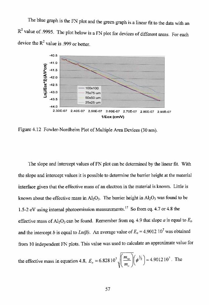
an The blue graph is the FN plot and the green graph is a linear fit to the data with
R' value of .9995. The plot below is a FN plot for devices of different areas. For each
device the R value is .999 or better.
^ -41.0 E ^ -41.5 < ~=- -42.0
5 -42.5 O ~> -43 0 c
_ l -43.5
-44.0
^ ^ - - - .
^***'>.^, ~"'"\ ^"" - ^^ .
"^"V.^^ X .
100x100
50x50 um 25x25 um
^ -- ^ "x
2.30E-07 2.40E-07 2.50E-07 2.60E-07 2.70E-07 2.80E-07 2.90E-07
1/Eox(cm/V)
Figure 4.12 Fowler-Nordheim Plot of Multiple Area Devices (30 nm).
The slope and intercept values of FN plot can be determined by the linear fit. With
the slope and intercept values it is possible to determine the barrier height at the material
interface given that the effective mass of an electron in the material is knovra. Little is
known about the effective mass in AI2O3. The barrier height in AI2O3 was found to be
1.5-2 eV using internal photoemission measurements.'^ So from eq. 4.7 or 4.8 the
effective mass of AI2O3 can be found. Remember from eq. 4.9 that slope a is equal to Eo
and the intercept b is equal to Ln(^). An average value of £<, = 4.9012 10 was obtained
from 10 independent FN plots. This value was used to calculate an approximate value for
the effective mass in equation 4.8, E^ = 6.82810 . r... \ m„
\^o J ^ 2 U 4.901210'. The
57

effective mass of an electron in AI2O3 is w„, = 0.152667w„. The coefficient values
obtained from the Fowler Nordheim plots are in good agreement with data presented in
(13) for similar oxide thickness and the same final anodization voltage of 20V.
Oxide Thickness Dependence
The area/perimeter analysis and tunneling mechanism analysis presented for this
oxide thickness was also performed on a sample with a thickness of 15 nm and a final
anodization voltage of lOV. The graph below is the I-V characteristics for this oxide.
3 3.5 4 Voltage (V)
Figure 4.13 I-V for devices of different TJ areas (15 nm).
The graph below shows a plot of current density versus voltage. This graph also
shows that the current densities are not equal. The plot also indicates the presence of a
perimeter affect.
58
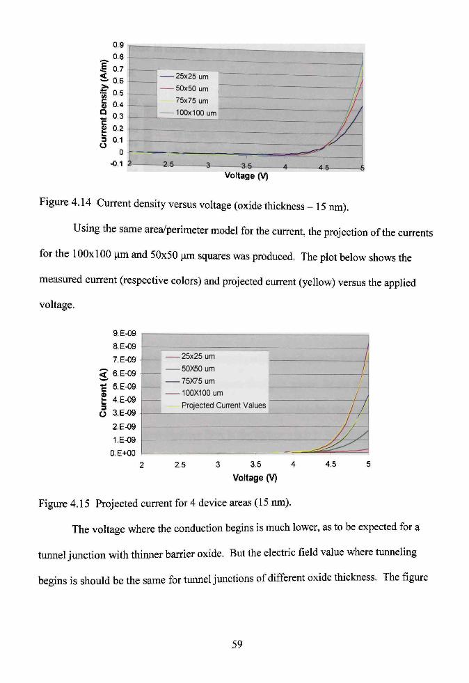
u.a
0.8 E 0 7
io.6 •f 0 5 O 0.4
!:i 0.3
£ 0.2
3 0.1 O
0 -0.1
-25x25 um 50x50 um
75x75 um
100x100 um
= : i / /
~ziiji 11 /
/ / /
^ • ^ ^
! ?-% 3 3 5 4T5 6
Voltage (V)
Figure 4.14 Current density versus voltage (oxide thickness - 15 nm).
Using the same area/perimeter model for the current, the projection of the currents
for the 100x100 p,m and 50x50 [im squares was produced. The plot below shows the
measured current (respective colors) and projected current (yellow) versus the applied
voltage.
9.E-09
8.E-09
7.E-09
< 6.E-09
^ 5.E-09
t 4.E-09
O 3.E-09
2.E-09
1.E-09
O.E+00
-25x25 um
- 50X50 um
- 75X75 um
- 100X100 um
Projected Current Values
2.5 3 3.5 4
Voltage (V)
4.5
Figure 4.15 Projected current for 4 device areas (15 nm).
The voltage where the conduction begins is much lower, as to be expected for a
tunnel junction with thinner barrier oxide. But the electric field value where ttmneling
begins is should be the same for tunnel junctions of different oxide thickness. The figure
59
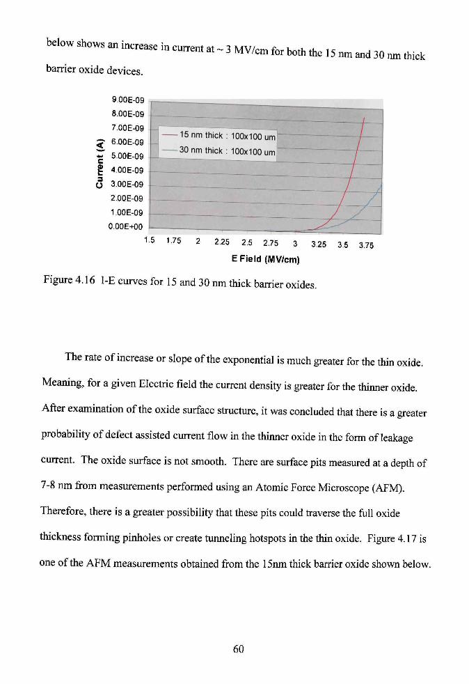
below shows an increase
barrier oxide devices.
in current at ~ 3 MV/cm for both the 15 nm and 30 nm thick
9.00E-09
8.00E-09
7.00E-09
^ 6.00E-09
^ 5.00E-09
g 4.00E-09
O 3.00E-09
2.00E-09
1 .OOE-09
O.OOE+00
15 1.75 2 2.25 2.5 2.75 3 3.25 3.5 3.75
E Field (MV/cm)
Figure 4.16 I-E curves for 15 and 30 nm thick barrier oxides.
The rate of increase or slope of the exponential is much greater for the thin oxide.
Meaning, for a given Electric field the current density is greater for the thinner oxide.
After examination of the oxide surface structure, it was concluded that there is a greater
probability of defect assisted current flow in the thinner oxide in the form of leakage
current. The oxide surface is not smooth. There are surface pits measured at a depth of
7-8 nm from measurements performed using an Atomic Force Microscope (AFM).
Therefore, there is a greater possibility that these pits could traverse the full oxide
thickness forming pinholes or create tunneling hotspots in the thin oxide. Figure 4.17 is
one of the AFM measurements obtained from the 15nm thick barrier oxide shown below.
60

Figure 4.17 AFM Profile of Barrier Oxide Surface (15nm)
One of the assumptions used in standard Fowler-Nordheim theory is that the surface
is flat and smooth'^. The RMS roughness for the thin oxide was determined to be 2 nm.
The turmeling characteristics for the 15 nm thick oxide are not as well behaved and as
stable as the 30 nm thick oxide. This instability is evident in the Fowler-Nordheim plot
below for the 15 nm thick tunnel junction barrier oxide. The intercepts and slopes of the
FN plot vary for tunnel junctions of different area. The FN plots for the 30 nm thick
oxide were consistent for different tunnel junction areas. This inconsistency in the
tunneling measurements for the 15 nm thick oxide is attributed to the surface structure of
the oxide films.
61
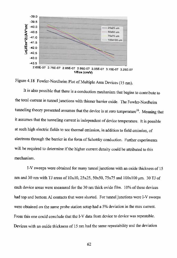
2.65E-07 2.75E-07 2.85E-07 2.95E-07 3.05E-07 3.15E-07 3.25E-07 1/Eox (cm/V)
Figure 4.18 Fowler-Nordheim Plot of Muhiple Area Devices (15 nm).
It is also possible that there is a conduction mechanism that begins to contribute to
the total current in tunnel junctions with thinner barrier oxide. The Fowler-Nordheim
tunneling theory presented assumes that the device is at zero temperature'^ Meaning that
it assumes that the tunneling current is independent of device temperature. It is possible
at such high electric fields to see thermal emission, in addition to field emission, of
electrons through the barrier in the form of Schottky conduction. Further experiments
will be required to determine if the higher current density could be attributed to this
mechanism.
I-V sweeps were obtained for many tunnel junctions with an oxide thickness of 15
nm and 30 nm with TJ areas of 10x10, 25x25, 50x50, 75x75 and 100x100 ^m. 30 TJ of
each device areas were measured for the 30 nm thick oxide film. 10% of these devices
had top and bottom Al contacts that were shorted. For tunnel junctions were I-V sweeps
were obtained on the same probe station setup had a 5% deviation in the max current.
From this one could conclude that the I-V data from device to device was repeatable.
Devices with an oxide thickness of 15 nm had the same repeatability and the deviation
62
nm was 15% in the max current. A much higher percentage of devices failed at the 15
thickness. Approximately 50% of the device measured failed due to shorted Al contacts.
The need to decrease the surface roughness of the tunnel junctions is apparent and is a
future objective for the project.
The Metal-Insulator-Metal Tunnel Junctions were characterized to determine
tiie dominant conduction mechanism through the AI2O3 barrier oxide. I-V curves were
acquired using measurement instrumentation designed for the project including a
LabVIEW-based data acquisition system. The I-V data was analyzed to investigate a
possible perimeter affect and to determine the dominant conduction mechanism. A slight
dependence on the perimeter was found in the tunnel junctions and a model was used to
project the tunneling current for devices of various sizes. The dominant conduction
mechanism found for the MIM TJ was Fowler-Nordheim tunneling for the device with a
barrier oxide of 30 nm. A combination of conduction mechanisms is expected for the
thinner (15nm) barrier oxide and future work will include the determination of this
conduction means.
63

CHAPTER 5
CONCLUSIONS AND DISCUSSION
Project Summary
The primary goal for this project was to develop a process for growing
reproducible high-quality AI2O3 barrier oxides and characterize the elecfrical properties
of the oxide. In order to accomplish this task a test device was designed. The scope of
the project included the full design, fabrication and characterization of the Metal-
Insulator-Metal Tunnel Junction test device.
The Tunnel Junction device design included the ability to test devices of different
areas, as well as the option to produce devices containing the desired AI2O3 barrier
thickness.
The fabrication of the MIM TJ devices included the design of the fabrication
process flow. The photomasks used in fabrication were designed in LASI 7 and
fabricated on high quality glass masks. Standard semiconductor processing techniques
were used to pattern the metal layers and to define regions for anodic oxide growth. The
process for growing anodic AI2O3 films was developed for this project. The growth
process was described in terms of the growth rate of the oxide films.
An instrumentation system was established to characterize the electrical
properties of the AI2O3 films. This system included the use of a probe station equipped
with an optical microscope and a data acquisition system comprised of computer
LabVIEW software that controls a Keithley 2400 Source/Meter. This system was used to
64
generate current versus voltage curves for TJ devices of different areas and different
thickness.
The I-V curves generated during testing were used to analyze the electrical
characteristics of the device. Comparisons between data collected on devices with the
same barrier oxide thickness but different device area showed that the current through the
jimction was slightly dependant on the device area. A model was suggested for this
dependence and the model was implemented in projecting the current for different device
areas.
The electric field regime where current through the device begins suggests that
Fowler-Nordheim conduction is present in the device. Using the Wentzel Kramers
Brillouin (WKB) approximation for Fowler-Nordheim theory a model was used to verify
the presence of Fowler-Nordheim tunneling. When the Fowler-Nordheim plot of the
tunneling data is linear the conduction mechanism is dominated by Fowler-Nordheim
tunneling. Thinner oxide samples show evidence of another mechanism contributing to
the conduction through the MIM Tunnel Junctions.
Future Work
This project was designed as a stepping-stone for a bigger project that will include
the addition of magnetoresistive layers to the AI2O3 barrier oxide layer. As described in
chapter 1 magnetoresistive devices use this barrier oxide layer. The barrier layer must be
thin, uniform and free of pinholes. The ftiture of this project will include scaling the
thickness of the barrier oxide to below 10 mn. as well as attempting to deposit an
65
aluminum layer that will be totally consumed during the oxidation process. For example
depositing a 6 nm Al film and anodizing the film to a thickness of-10 nm.
Improvements in the uniformity of the AI2O3 barrier oxide layer are needed. Possible
fabrication modification might include a pre-anodization anneal of the bottom Al contact,
using a slower Al deposition rate to improve the surface roughness of the Al contact and
also slowing the growth of the AI2O3 film by reducing the current density used during
anodization.
Following this achievement, the magnetoresistive tunnel junction (MJT) will be
designed to include a pinned ferromagnetic layer and a floating ferromagnetic layer. In
free ferromagnetic layers the magnetic orientation of a film can be changed by applying a
saturating magnetic field and will exhibit a hysteretic property, meaning that the film will
remain this orientation after the field is removed.^ The orientation of the film can be
fixed by placing an anti-ferromagnetic layer in contact with the ferromagnetic layer.
Determining the materials and the processes for depositing the materials will be included
in the future work of the MTJ development, as well as testing the MJT. Using a four-
point probe configuration the resistance of the MJT can be plotted with respect to an
external field.
This work would then lead to the development of a Magnetic Readhead device.
66
REFERENCES
1. J. M. Slaughter, E. Y. Chen, R. Whig, B. N. Engel, J. Janesky and S. Tehrani, JOM-e 52, No. 6 (2000).
2. B. J. Jonsson-Akerman, R. Escudero, C. Leighton, S. Kim, Ivan K. SchuUer and D. A. Rabson. Appl. Phys. Lett. 77, 1870 (2000).
3. C. H. Tsang, Et. Al, IBM J. Res. Develop. 42, No. 1, Jan. 1998.
4. Serway, Physics: For Scientists and Engineers, 5th Ed., Vol.2, Saunders College Publishing, Orlando, Fl, 2000
5. Campbell. The Science and Engineering of Microelectronic Fabrication, Oxford University Press, New York, 2001.
6. R. D. Knight, Physics: A Contemporary Perspective Vol. 2, Addison Wesley, New York, 1997.
7. http://www.mc.mat.shibaura-ft.ac.jp/~plaza/chap219.html
8. http://electrochem.cwru.edu/ed/encycl/art-a02-anodizing.htm
9. T. W. Hickmott, J. Appl. Phys. 93, No. 6, 3461 (2003)
10 M Zecchino, A. G. Olsak, "High Speed Surface Measurement with Lateral Scanning White Light Interferometry" (AN502), Veeco Instruments, Inc., 2650 E. Elvira Road, Tuscon,AZ 85706 (2001)
11. http://lpcl.clpccd.cc.ca.us/lpc/physics/pdf/relation.pdf
12. A. K. Jonscher, Dielectric Relaxation in Solids (Chelsea Dielectrics, London, 1983),
p. 22
13. T. W. Hickmott, J. Appl. Phys. 87, No. 11, 7903-12 (2000)
14 B Domenges,H. Murray, P. Schwindenhammer and G.Imbert,Semicond.Sci.
Technol., Vol. 19, No. 2, 191-197 (2004)
15. Y. Khlifi, K. Kassmi, L. Roubi, R. Maimouni, M.J. Condensed Matter, Vol. 3. No. 1,
1 June 2000
16. R. G. Forbes, J. Vac. Sci. Technol. B 17, 526 (1999)
17. A. M. Goodman, J. Appl. Phys. 41, 2176 (1970)
67

PERMISSION TO COPY
In presenting this thesis in partial fulfillment of the requirements for a master's
degree at Texas Tech University or Texas Tech University Healtii Sciences Center, I
agree that the Library and my major department shall make it freely available for
research purposes. Permission to copy this thesis for scholarly purposes may be
granted by the Director of the Library or my major professor. It is understood that any
copying or publication of this thesis for financial gain shall not be allowed without my
further written permission and that any user may be liable for copyright infringement.
Agree (Permission is granted.)
Disagree (Permission is not granted.)