design for manufacturability - smta · design for manufacturability verify that the design is...
TRANSCRIPT
design develop deliver advanced technologyCopyright © 2016 by original author Benchmark Electronics, Inc. Not to be
reproduced or used in any means without written permission by Benchmark.
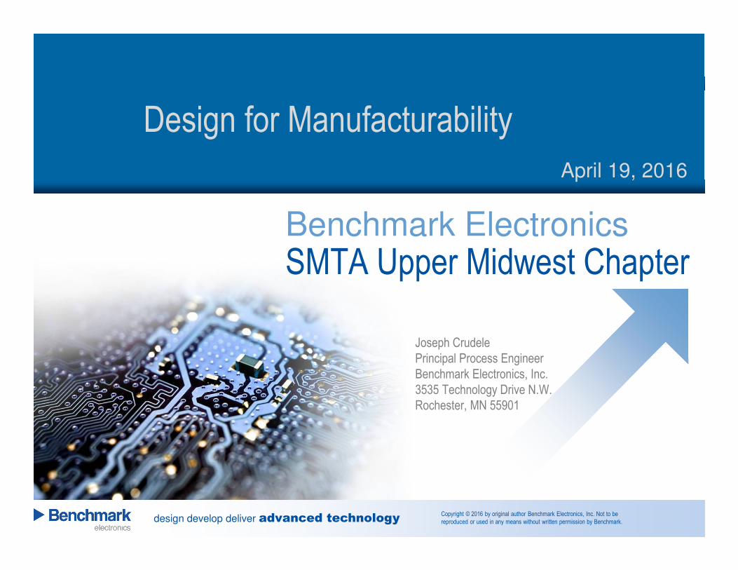
Benchmark Electronics
April 19, 2016
SMTA Upper Midwest Chapter
Design for Manufacturability
Joseph Crudele
Principal Process Engineer
Benchmark Electronics, Inc.
3535 Technology Drive N.W.
Rochester, MN 55901
design develop deliver advanced technologyCopyright © 2016 by original author Benchmark Electronics, Inc. Not to be
reproduced or used in any means without written permission by Benchmark.2
Design for Manufacturability
� Verify that the design is producible by CM and CM’s suppliers.
� Determining the best balance between
� component cost and CM’s manufacturing cost.
� component lead time and CM’s manufacturing lead time.
Benefits of DFM
� Early identification of design, process flow and tooling issues.
� Lower cost, shorter lead-time.
� Reduced process variation
� Early engagement = lower cost + higher quality
This presentation will explore the basics of a DFM and build summary for
printed circuit assemblies.
The recommendations, guidelines, design rules, and other considerations contained in this document are provided “as
is”, with no warranty whatsoever. Any use or implementation of the recommendations, guidelines, rules, or other
considerations in this document are undertaken at the sole risk of the user and its personnel.
Design for Manufacture
design develop deliver advanced technologyCopyright © 2016 by original author Benchmark Electronics, Inc. Not to be
reproduced or used in any means without written permission by Benchmark.3
When Benchmark performs a DFM
� Manufacturability is considered during the project Proposal phase.
� A DFM review is an output of the Design phase process.
� Manufacturability issues identified in the Prototype phase, Pre-Production
phase, Qualification, and Production phases might drive design changes.
� DFM is an output when reviewing customer engineering change (EC) requests.
(before)
Build Summary Review
� Typically occurs after 1st time build, NPI Build, or major design change.
� When a Process Feedback System triggers a clip limit .
(after)
What does your company call this initial build?
Design for Manufacture
design develop deliver advanced technologyCopyright © 2016 by original author Benchmark Electronics, Inc. Not to be
reproduced or used in any means without written permission by Benchmark.4
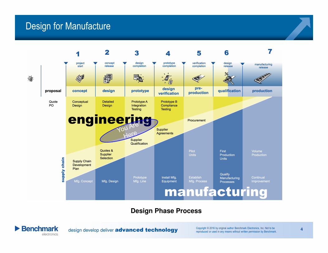
Design for Manufacture
Design Phase Process
design develop deliver advanced technologyCopyright © 2016 by original author Benchmark Electronics, Inc. Not to be
reproduced or used in any means without written permission by Benchmark.5
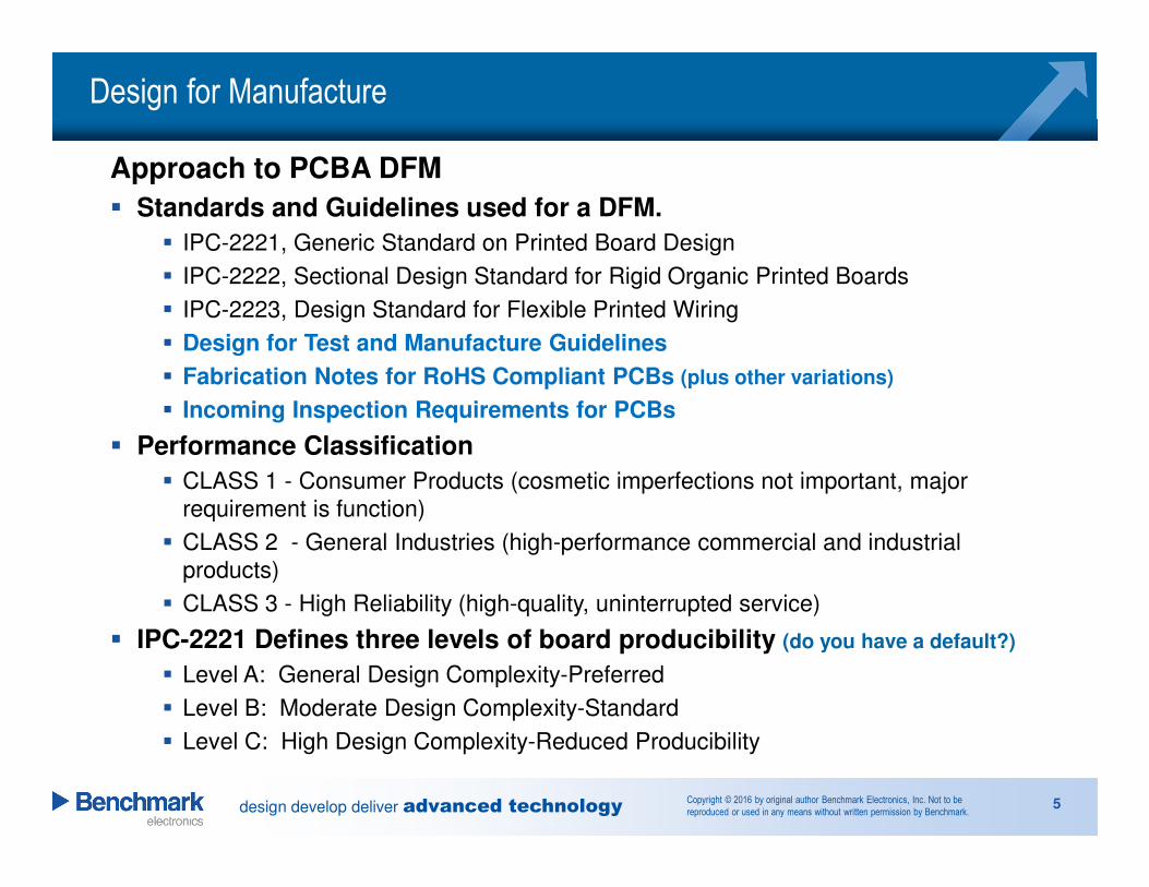
Approach to PCBA DFM
� Standards and Guidelines used for a DFM.
� IPC-2221, Generic Standard on Printed Board Design
� IPC-2222, Sectional Design Standard for Rigid Organic Printed Boards
� IPC-2223, Design Standard for Flexible Printed Wiring
� Design for Test and Manufacture Guidelines
� Fabrication Notes for RoHS Compliant PCBs (plus other variations)
� Incoming Inspection Requirements for PCBs
� Performance Classification
� CLASS 1 - Consumer Products (cosmetic imperfections not important, major
requirement is function)
� CLASS 2 - General Industries (high-performance commercial and industrial
products)
� CLASS 3 - High Reliability (high-quality, uninterrupted service)
� IPC-2221 Defines three levels of board producibility (do you have a default?)
� Level A: General Design Complexity-Preferred
� Level B: Moderate Design Complexity-Standard
� Level C: High Design Complexity-Reduced Producibility
Design for Manufacture
design develop deliver advanced technologyCopyright © 2016 by original author Benchmark Electronics, Inc. Not to be
reproduced or used in any means without written permission by Benchmark.6
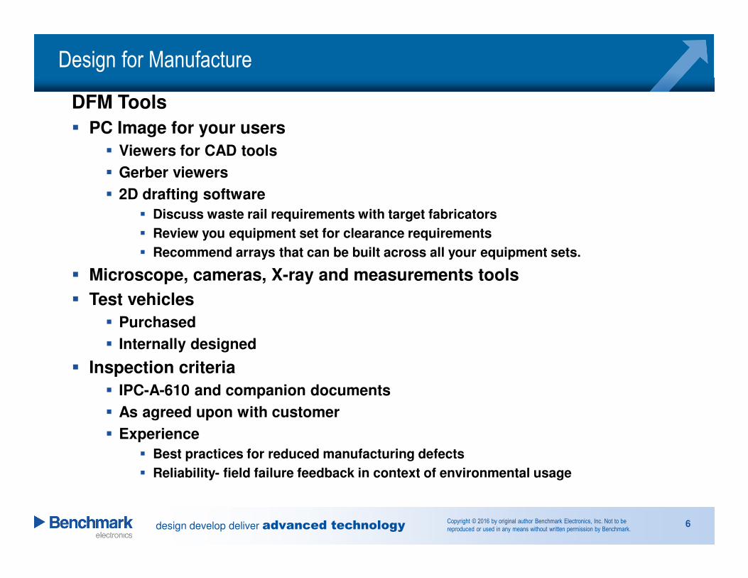
DFM Tools
� PC Image for your users
� Viewers for CAD tools
� Gerber viewers
� 2D drafting software
� Discuss waste rail requirements with target fabricators
� Review you equipment set for clearance requirements
� Recommend arrays that can be built across all your equipment sets.
� Microscope, cameras, X-ray and measurements tools
� Test vehicles
� Purchased
� Internally designed
� Inspection criteria
� IPC-A-610 and companion documents
� As agreed upon with customer
� Experience
� Best practices for reduced manufacturing defects
� Reliability- field failure feedback in context of environmental usage
Design for Manufacture
design develop deliver advanced technologyCopyright © 2016 by original author Benchmark Electronics, Inc. Not to be
reproduced or used in any means without written permission by Benchmark.
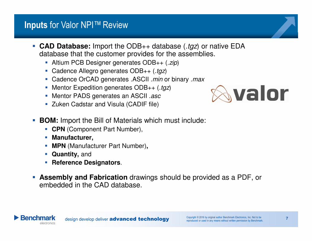
� CAD Database: Import the ODB++ database (.tgz) or native EDA database that the customer provides for the assemblies.
� Altium PCB Designer generates ODB++ (.zip)
� Cadence Allegro generates ODB++ (.tgz)
� Cadence OrCAD generates .ASCII .min or binary .max
� Mentor Expedition generates ODB++ (.tgz)
� Mentor PADS generates an ASCII .asc
� Zuken Cadstar and Visula (CADIF file)
� BOM: Import the Bill of Materials which must include:
� CPN (Component Part Number),
� Manufacturer,
� MPN (Manufacturer Part Number),
� Quantity, and
� Reference Designators.
� Assembly and Fabrication drawings should be provided as a PDF, or embedded in the CAD database.
7
Inputs for Valor NPI™Review
design develop deliver advanced technologyCopyright © 2016 by original author Benchmark Electronics, Inc. Not to be
reproduced or used in any means without written permission by Benchmark.8
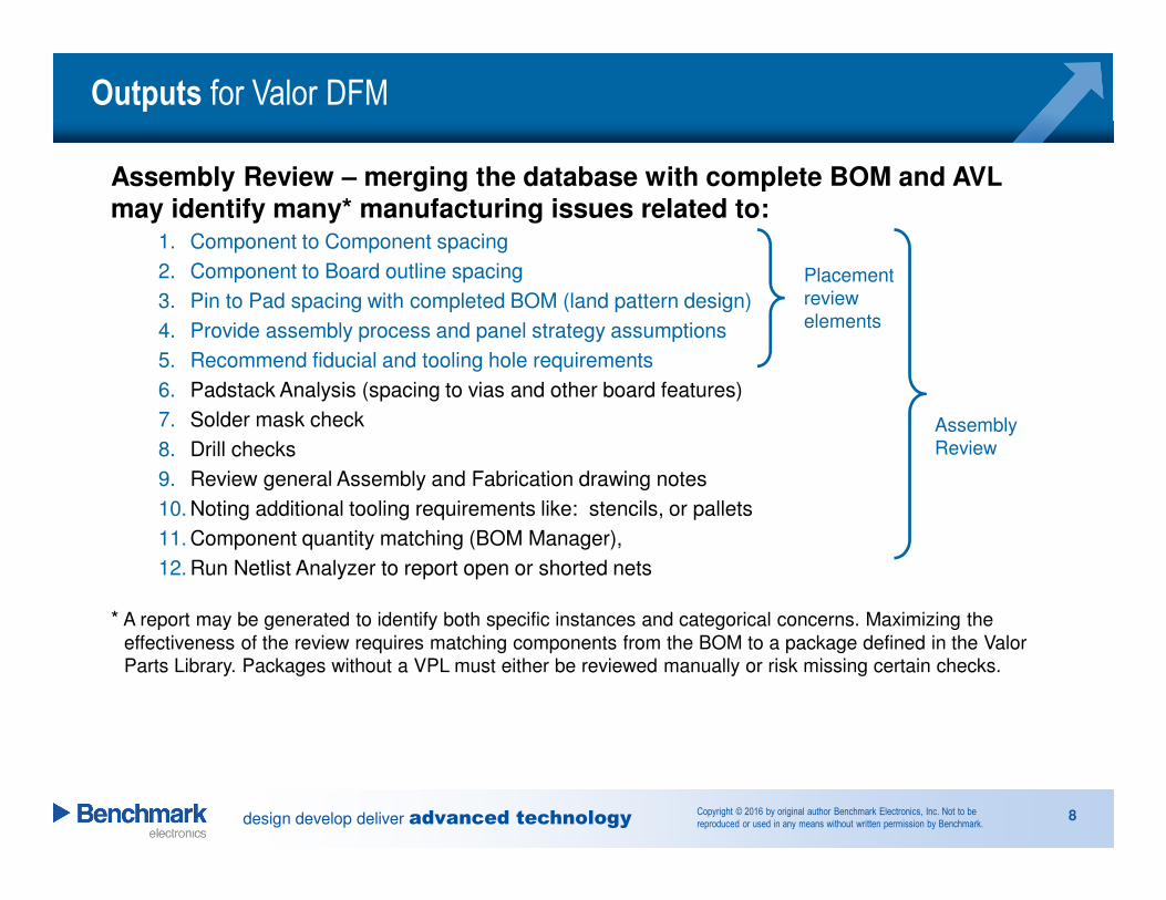
Assembly Review – merging the database with complete BOM and AVL may identify many* manufacturing issues related to:
1. Component to Component spacing
2. Component to Board outline spacing
3. Pin to Pad spacing with completed BOM (land pattern design)
4. Provide assembly process and panel strategy assumptions
5. Recommend fiducial and tooling hole requirements
6. Padstack Analysis (spacing to vias and other board features)
7. Solder mask check
8. Drill checks
9. Review general Assembly and Fabrication drawing notes
10. Noting additional tooling requirements like: stencils, or pallets
11. Component quantity matching (BOM Manager),
12. Run Netlist Analyzer to report open or shorted nets
* A report may be generated to identify both specific instances and categorical concerns. Maximizing the
effectiveness of the review requires matching components from the BOM to a package defined in the Valor
Parts Library. Packages without a VPL must either be reviewed manually or risk missing certain checks.
Placement
review
elements
Assembly
Review
Outputs for Valor DFM
design develop deliver advanced technologyCopyright © 2016 by original author Benchmark Electronics, Inc. Not to be
reproduced or used in any means without written permission by Benchmark.
DFM Review Definitions
9
Review Definitions:
� Panel Drawing (assembly array) - optimizes the number, and
orientation of the PCBs in an array that best fits the required assembly
processes.
� Panel Strategy - the PCB can be one of the most expensive parts of the
assembly and certainly the most custom. Its shape, size, and
panelization will have the single, largest impact on enabling the use of
preferred processes. Optimization of the assembly array may also
significantly impact the cost of the bare PCB. This is also dependent on
cost of the assembly and production volume.
design develop deliver advanced technologyCopyright © 2016 by original author Benchmark Electronics, Inc. Not to be
reproduced or used in any means without written permission by Benchmark.10
DFM Checklist
Statement of what is being reviewed (part 1)
� Customer
� Assembly Name
� Assembly Part Number
� Date of Review
� Who is doing the review: (review team)
� Documented process flow for product
� Classification Codes: Required, Recommended, Observation, FYI
� Assembly assumptions: Solder alloy, flux chemistry, projected annual quantity,
dimensions, layer count, total copper weight in stack-up, assembly processes
required, IPC class requirements for assembly and fabrication.
design develop deliver advanced technologyCopyright © 2016 by original author Benchmark Electronics, Inc. Not to be
reproduced or used in any means without written permission by Benchmark.11
DFM Checklist
Standard list of questions should be answered (part 2)
� It is just as important to lock down what is correct with a design…
� Solder mask approach on land patterns, vias and test points. Is the
intended exposed copper not excessively impacted by the mask approach?
� Is board finish appropriate?
� Panelization based on size, shape and thickness:
� Copper to board edge clearance
� Are tooling holes sizes and locations acceptable?
� Are useable fiducials provided on both sides of the PCB?
� Are panel fiducials provided/required?
� Flashing with tabs of what type? (solid, v-score, breakaway)
� Number of circuits per array?
� Orientation of boards?
� Are image rejection marks required?
� Are all breakaway tabs clear of any overhanging components?
design develop deliver advanced technologyCopyright © 2016 by original author Benchmark Electronics, Inc. Not to be
reproduced or used in any means without written permission by Benchmark.12
DFM Checklist
(part 2 continued)
� Do components follow proper component to component spacing?
� SMT to SMT
� Mixed Technology
� Plated Through Hole
� Are thieving pads required?
� Is bottom side SMT to topside PTH barrels clearance acceptable?
� Is the board designed to minimize process steps?
� Are there any new technologies on the board?
� Are BGA lands acceptable?
� Are thermal relief techniques used on power and ground layers sufficient
to enable barrel fill for PTH components?
� Are barrel sizes appropriate for PTH leads considering total copper in
stack-up?
design develop deliver advanced technologyCopyright © 2016 by original author Benchmark Electronics, Inc. Not to be
reproduced or used in any means without written permission by Benchmark.13
DFM Checklist
Sharelist (part 3)
� Sharelist items are listed at the end of the review. They are given a item
number, priority, title and open/closed status.
� They may illustrate a single opportunity in the design, or frame an issue
that impacts many components, or features across the assembly.
� Sharelist items are a useful discussion tool. The status and discussion can
be tracked by date until eventually closed.
� Sometimes design constraints may not allow changes to be made to the
design and those instances are important to note.
design develop deliver advanced technologyCopyright © 2016 by original author Benchmark Electronics, Inc. Not to be
reproduced or used in any means without written permission by Benchmark.
How DFM is tied to IPC-A-610
14
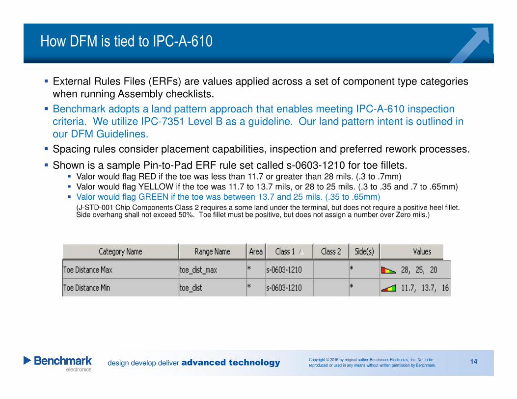
� External Rules Files (ERFs) are values applied across a set of component type categories
when running Assembly checklists.
� Benchmark adopts a land pattern approach that enables meeting IPC-A-610 inspection
criteria. We utilize IPC-7351 Level B as a guideline. Our land pattern intent is outlined in
our DFM Guidelines.
� Spacing rules consider placement capabilities, inspection and preferred rework processes.
� Shown is a sample Pin-to-Pad ERF rule set called s-0603-1210 for toe fillets. � Valor would flag RED if the toe was less than 11.7 or greater than 28 mils. (.3 to .7mm)
� Valor would flag YELLOW if the toe was 11.7 to 13.7 mils, or 28 to 25 mils. (.3 to .35 and .7 to .65mm)
� Valor would flag GREEN if the toe was between 13.7 and 25 mils. (.35 to .65mm)
(J-STD-001 Chip Components Class 2 requires a some land under the terminal, but does not require a positive heel fillet. Side overhang shall not exceed 50%. Toe fillet must be positive, but does not assign a number over Zero mils.)
design develop deliver advanced technologyCopyright © 2016 by original author Benchmark Electronics, Inc. Not to be
reproduced or used in any means without written permission by Benchmark.
How Valor NPI™ Works: External Rule Files (9.2)
15
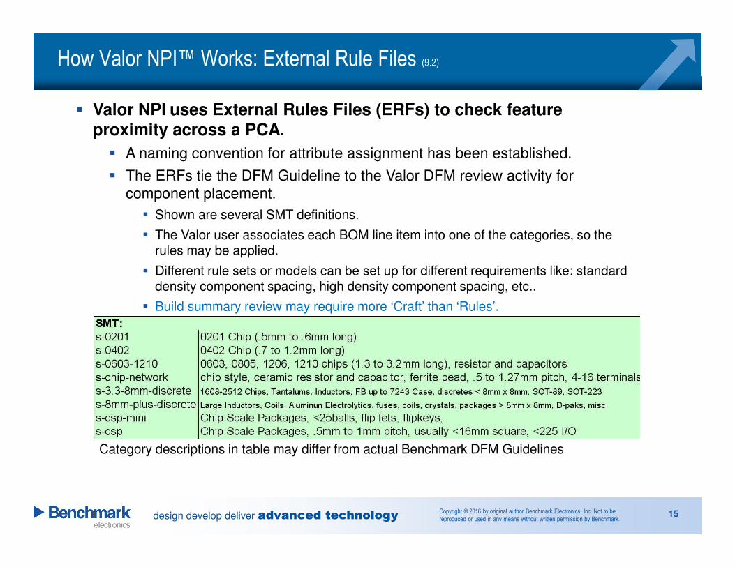
� Valor NPI uses External Rules Files (ERFs) to check feature proximity across a PCA.
� A naming convention for attribute assignment has been established.
� The ERFs tie the DFM Guideline to the Valor DFM review activity for
component placement.
� Shown are several SMT definitions.
� The Valor user associates each BOM line item into one of the categories, so the rules may be applied.
� Different rule sets or models can be set up for different requirements like: standard density component spacing, high density component spacing, etc..
� Build summary review may require more ‘Craft’ than ‘Rules’.
Category descriptions in table may differ from actual Benchmark DFM Guidelines
design develop deliver advanced technologyCopyright © 2016 by original author Benchmark Electronics, Inc. Not to be
reproduced or used in any means without written permission by Benchmark.
How Valor NPI™ Works: ERFs
16
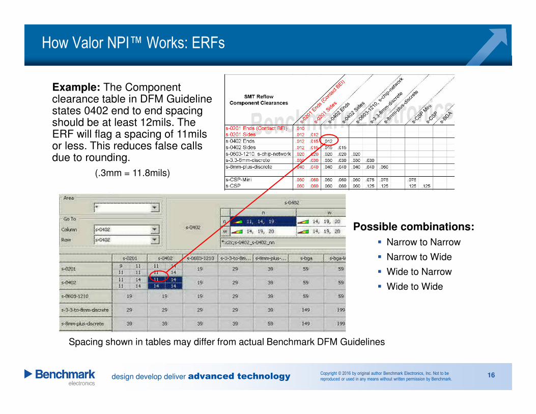
Example: The Component clearance table in DFM Guideline states 0402 end to end spacing should be at least 12mils. The ERF will flag a spacing of 11mils or less. This reduces false calls due to rounding.
(.3mm = 11.8mils)
Possible combinations:
� Narrow to Narrow
� Narrow to Wide
� Wide to Narrow
� Wide to Wide
Spacing shown in tables may differ from actual Benchmark DFM Guidelines
design develop deliver advanced technologyCopyright © 2016 by original author Benchmark Electronics, Inc. Not to be
reproduced or used in any means without written permission by Benchmark.
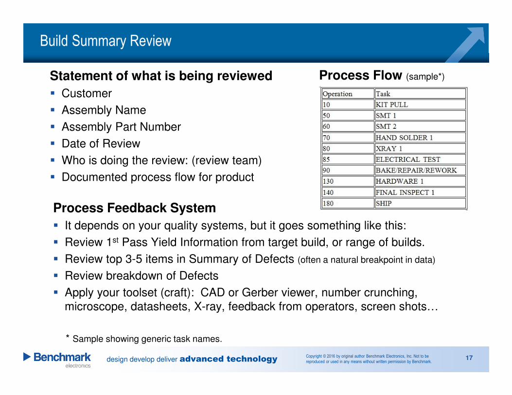
Build Summary Review
Statement of what is being reviewed
� Customer
� Assembly Name
� Assembly Part Number
� Date of Review
� Who is doing the review: (review team)
� Documented process flow for product
17
Process Flow (sample*)
Process Feedback System
� It depends on your quality systems, but it goes something like this:
� Review 1st Pass Yield Information from target build, or range of builds.
� Review top 3-5 items in Summary of Defects (often a natural breakpoint in data)
� Review breakdown of Defects
� Apply your toolset (craft): CAD or Gerber viewer, number crunching,
microscope, datasheets, X-ray, feedback from operators, screen shots…
* Sample showing generic task names.
design develop deliver advanced technologyCopyright © 2016 by original author Benchmark Electronics, Inc. Not to be
reproduced or used in any means without written permission by Benchmark.
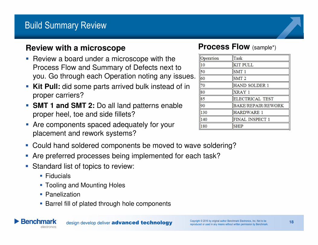
Build Summary Review
Review with a microscope
� Review a board under a microscope with the
Process Flow and Summary of Defects next to
you. Go through each Operation noting any issues.
� Kit Pull: did some parts arrived bulk instead of in
proper carriers?
� SMT 1 and SMT 2: Do all land patterns enable
proper heel, toe and side fillets?
� Are components spaced adequately for your
placement and rework systems?
18
� Could hand soldered components be moved to wave soldering?
� Are preferred processes being implemented for each task?
� Standard list of topics to review:
� Fiducials
� Tooling and Mounting Holes
� Panelization
� Barrel fill of plated through hole components
Process Flow (sample*)
design develop deliver advanced technologyCopyright © 2016 by original author Benchmark Electronics, Inc. Not to be
reproduced or used in any means without written permission by Benchmark.
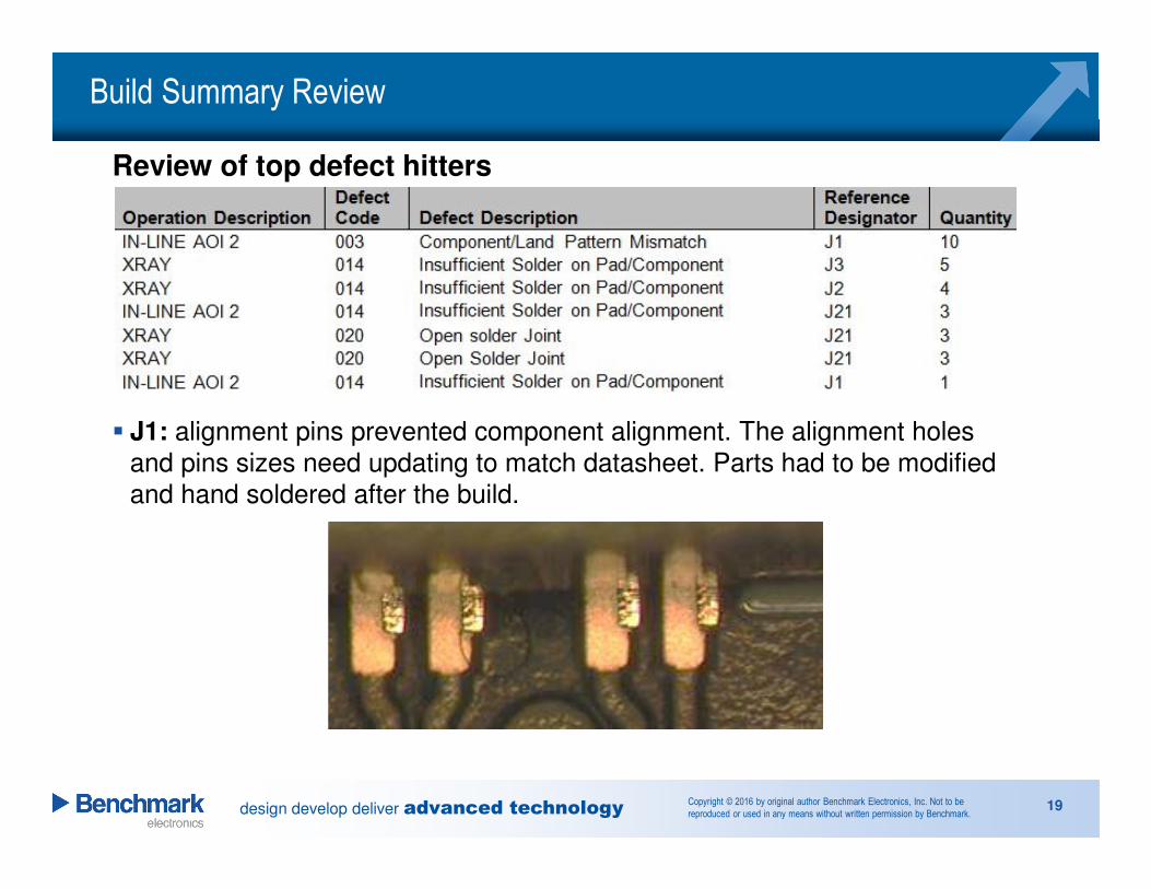
Build Summary Review
Review of top defect hitters
� J1: alignment pins prevented component alignment. The alignment holes
and pins sizes need updating to match datasheet. Parts had to be modified
and hand soldered after the build.
19
design develop deliver advanced technologyCopyright © 2016 by original author Benchmark Electronics, Inc. Not to be
reproduced or used in any means without written permission by Benchmark.
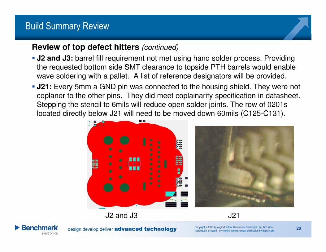
Build Summary Review
Review of top defect hitters (continued)
� J2 and J3: barrel fill requirement not met using hand solder process. Providing
the requested bottom side SMT clearance to topside PTH barrels would enable
wave soldering with a pallet. A list of reference designators will be provided.
� J21: Every 5mm a GND pin was connected to the housing shield. They were not
coplaner to the other pins. They did meet coplainarity specification in datasheet.
Stepping the stencil to 6mils will reduce open solder joints. The row of 0201s
located directly below J21 will need to be moved down 60mils (C125-C131).
J2 and J3 J21
20
design develop deliver advanced technologyCopyright © 2016 by original author Benchmark Electronics, Inc. Not to be
reproduced or used in any means without written permission by Benchmark.
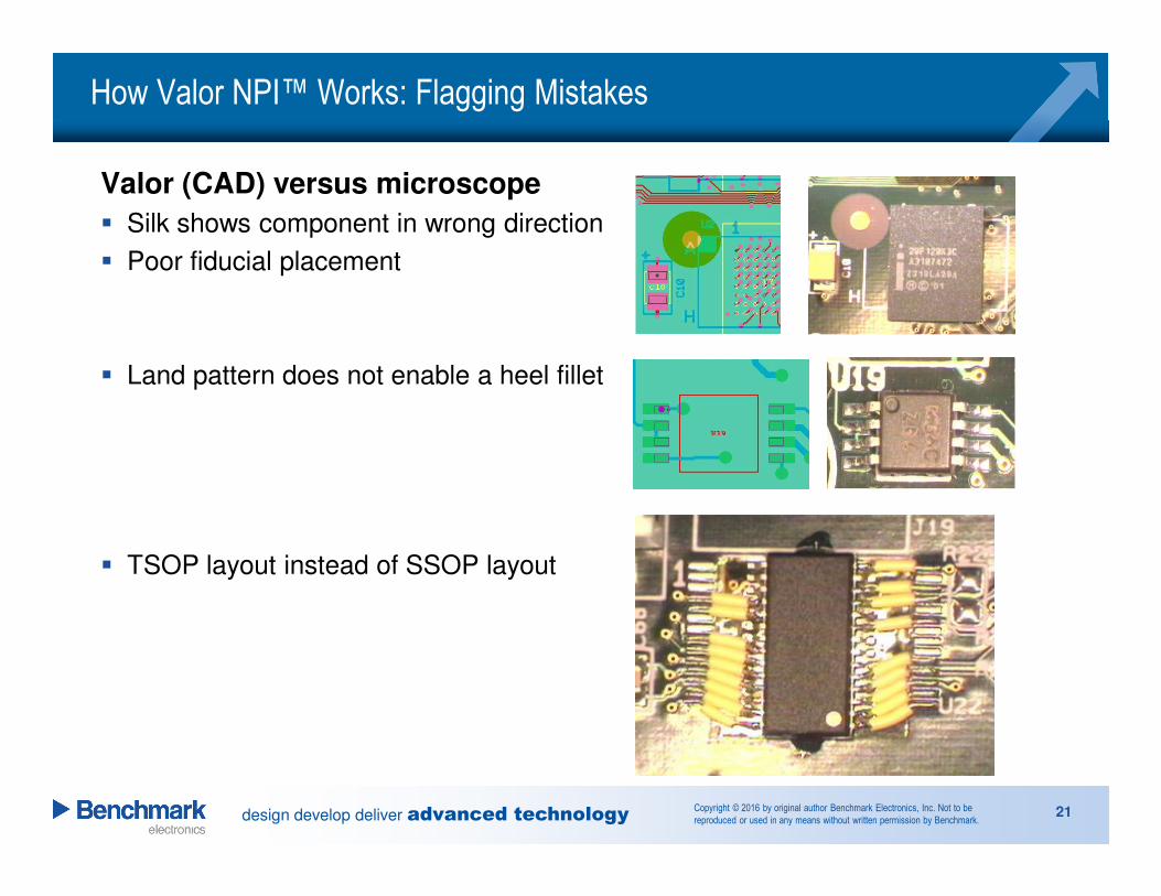
How Valor NPI™ Works: Flagging Mistakes
21
Valor (CAD) versus microscope
� Silk shows component in wrong direction
� Poor fiducial placement
� Land pattern does not enable a heel fillet
� TSOP layout instead of SSOP layout
design develop deliver advanced technologyCopyright © 2016 by original author Benchmark Electronics, Inc. Not to be
reproduced or used in any means without written permission by Benchmark.
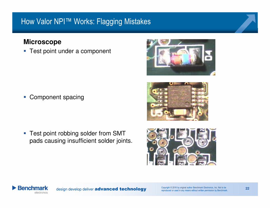
How Valor NPI™ Works: Flagging Mistakes
22
Microscope
� Test point under a component
� Component spacing
� Test point robbing solder from SMT
pads causing insufficient solder joints.
design develop deliver advanced technologyCopyright © 2016 by original author Benchmark Electronics, Inc. Not to be
reproduced or used in any means without written permission by Benchmark.
SMTA Presentation: Design for Manufacture (April 19, 2016)
23
What has been covered?
� DFM Inputs and outputs
� Build Summary Review
� DFM Placement and Assembly Review
� Sample system structure
To Follow:
� Several high level topics found in a DFM Guideline
� Examples for Discussion
design develop deliver advanced technologyCopyright © 2016 by original author Benchmark Electronics, Inc. Not to be
reproduced or used in any means without written permission by Benchmark.24
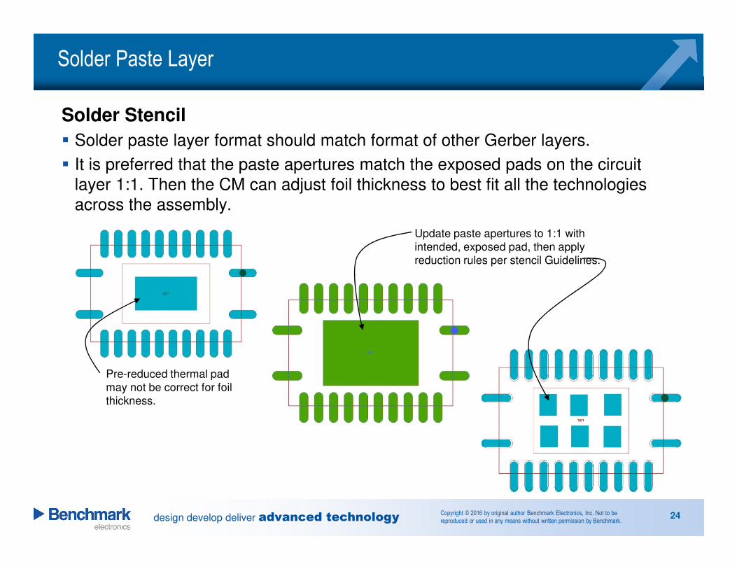
Solder Stencil
� Solder paste layer format should match format of other Gerber layers.
� It is preferred that the paste apertures match the exposed pads on the circuit
layer 1:1. Then the CM can adjust foil thickness to best fit all the technologies
across the assembly.
Update paste apertures to 1:1 with
intended, exposed pad, then apply
reduction rules per stencil Guidelines.
Pre-reduced thermal pad
may not be correct for foil
thickness.
Solder Paste Layer
design develop deliver advanced technologyCopyright © 2016 by original author Benchmark Electronics, Inc. Not to be
reproduced or used in any means without written permission by Benchmark.25
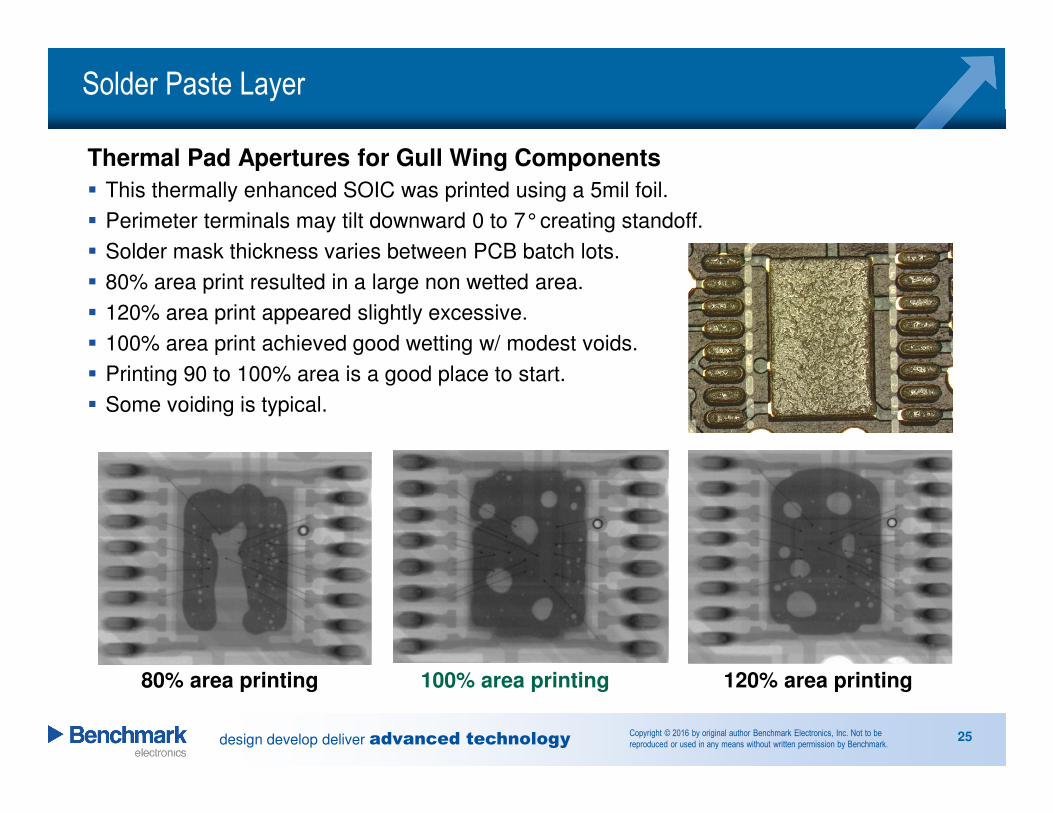
Thermal Pad Apertures for Gull Wing Components
� This thermally enhanced SOIC was printed using a 5mil foil.
� Perimeter terminals may tilt downward 0 to 7°creating standoff.
� Solder mask thickness varies between PCB batch lots.
� 80% area print resulted in a large non wetted area.
� 120% area print appeared slightly excessive.
� 100% area print achieved good wetting w/ modest voids.
� Printing 90 to 100% area is a good place to start.
� Some voiding is typical.
80% area printing 100% area printing 120% area printing
Solder Paste Layer
design develop deliver advanced technologyCopyright © 2016 by original author Benchmark Electronics, Inc. Not to be
reproduced or used in any means without written permission by Benchmark.
Solder Paste Layer
Bottom Terminal Components (BTC)
� The A-610F (current revision) sets the voiding of the thermal plane on a BTC to
an AABUS condition for all classes of product (clause 8.3.13: Thermal plane
void criteria shall be established between the Manufacturer and User.)
� As noted in IPC 7093 (Design and Assembly Process Implementation for
Bottom Termination Components: clause 7.6.1) most vendors will set a
minimum of 50% coverage based on thermal transfer needs of the particular
component. This number could certainly change based on the customer’s
needs. Clause 6.1.5.3 in the same document discusses voiding in relation to
via-in-pad, and states that small distributed voids are unlikely to cause
degradation of performance, but large voids should be avoided.
� As for BGA terminals, yes there is a difference, collapsing balls are allowed to
show voiding (up to 30% of each ball image area). No criteria is established
(recently changed from no voids allowed) for non-collapsing balls.
26
design develop deliver advanced technologyCopyright © 2016 by original author Benchmark Electronics, Inc. Not to be
reproduced or used in any means without written permission by Benchmark.
Solder Paste Layer
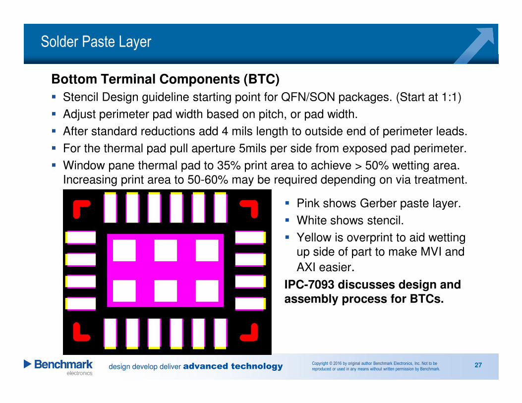
Bottom Terminal Components (BTC)
� Stencil Design guideline starting point for QFN/SON packages. (Start at 1:1)
� Adjust perimeter pad width based on pitch, or pad width.
� After standard reductions add 4 mils length to outside end of perimeter leads.
� For the thermal pad pull aperture 5mils per side from exposed pad perimeter.
� Window pane thermal pad to 35% print area to achieve > 50% wetting area.
Increasing print area to 50-60% may be required depending on via treatment.
� Pink shows Gerber paste layer.
� White shows stencil.
� Yellow is overprint to aid wetting
up side of part to make MVI and
AXI easier.
IPC-7093 discusses design and assembly process for BTCs.
27
design develop deliver advanced technologyCopyright © 2016 by original author Benchmark Electronics, Inc. Not to be
reproduced or used in any means without written permission by Benchmark.28
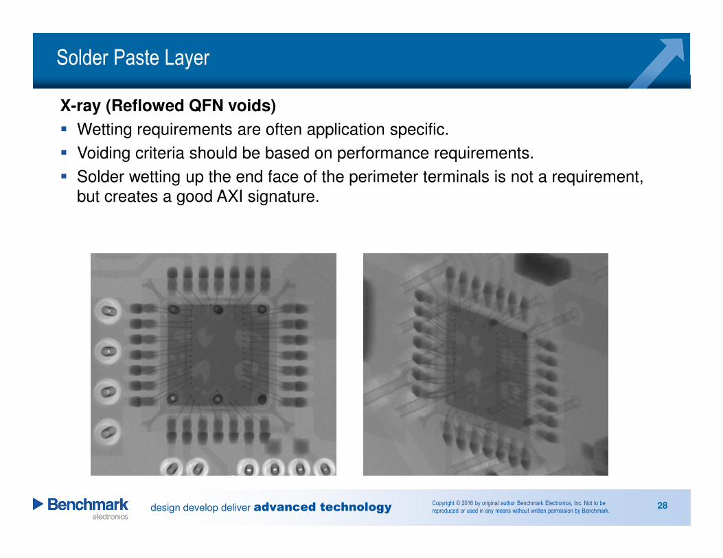
X-ray (Reflowed QFN voids)
� Wetting requirements are often application specific.
� Voiding criteria should be based on performance requirements.
� Solder wetting up the end face of the perimeter terminals is not a requirement,
but creates a good AXI signature.
Solder Paste Layer
design develop deliver advanced technologyCopyright © 2016 by original author Benchmark Electronics, Inc. Not to be
reproduced or used in any means without written permission by Benchmark.29
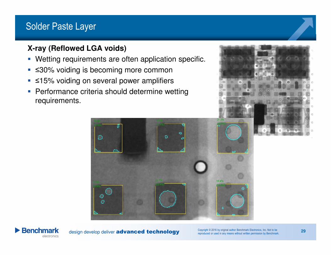
X-ray (Reflowed LGA voids)
� Wetting requirements are often application specific.
� ≤30% voiding is becoming more common
� ≤15% voiding on several power amplifiers
� Performance criteria should determine wetting
requirements.
Solder Paste Layer
design develop deliver advanced technologyCopyright © 2016 by original author Benchmark Electronics, Inc. Not to be
reproduced or used in any means without written permission by Benchmark.30
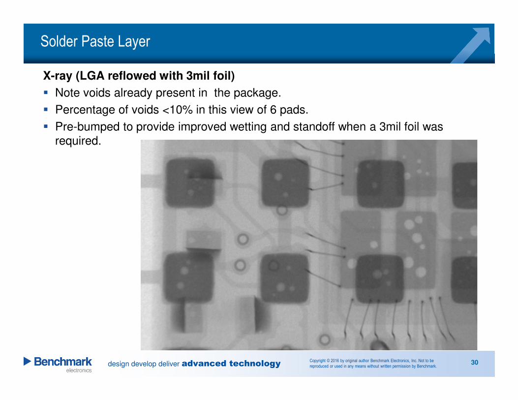
X-ray (LGA reflowed with 3mil foil)
� Note voids already present in the package.
� Percentage of voids <10% in this view of 6 pads.
� Pre-bumped to provide improved wetting and standoff when a 3mil foil was
required.
Solder Paste Layer
design develop deliver advanced technologyCopyright © 2016 by original author Benchmark Electronics, Inc. Not to be
reproduced or used in any means without written permission by Benchmark.31
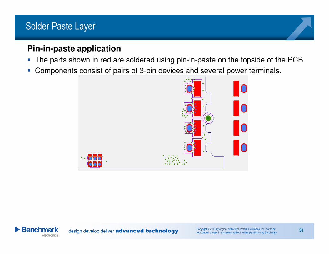
Pin-in-paste application
� The parts shown in red are soldered using pin-in-paste on the topside of the PCB.
� Components consist of pairs of 3-pin devices and several power terminals.
Solder Paste Layer
design develop deliver advanced technologyCopyright © 2016 by original author Benchmark Electronics, Inc. Not to be
reproduced or used in any means without written permission by Benchmark.32
Pin-in-paste application
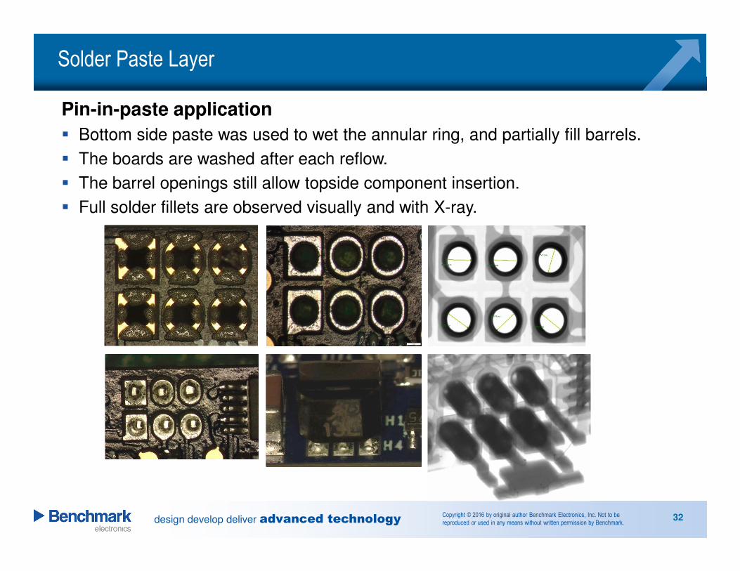
� Bottom side paste was used to wet the annular ring, and partially fill barrels.
� The boards are washed after each reflow.
� The barrel openings still allow topside component insertion.
� Full solder fillets are observed visually and with X-ray.
Solder Paste Layer
design develop deliver advanced technologyCopyright © 2016 by original author Benchmark Electronics, Inc. Not to be
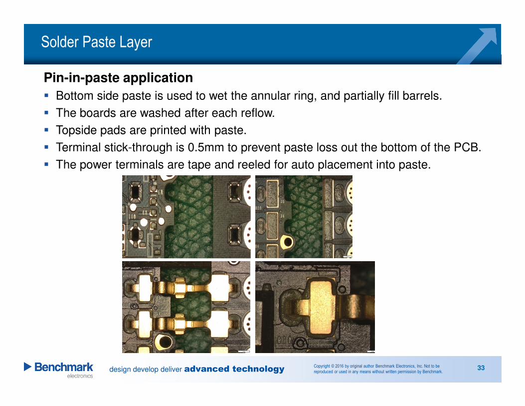
reproduced or used in any means without written permission by Benchmark.33
Pin-in-paste application
� Bottom side paste is used to wet the annular ring, and partially fill barrels.
� The boards are washed after each reflow.
� Topside pads are printed with paste.
� Terminal stick-through is 0.5mm to prevent paste loss out the bottom of the PCB.
� The power terminals are tape and reeled for auto placement into paste.
Solder Paste Layer
design develop deliver advanced technologyCopyright © 2016 by original author Benchmark Electronics, Inc. Not to be
reproduced or used in any means without written permission by Benchmark.34
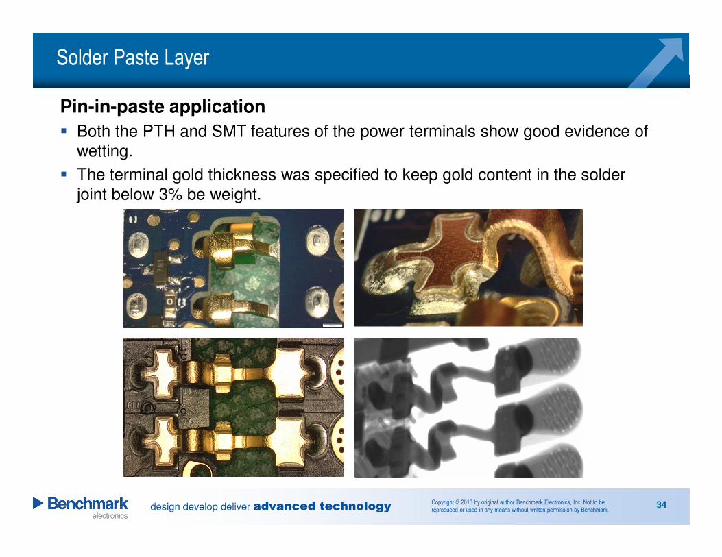
Pin-in-paste application
� Both the PTH and SMT features of the power terminals show good evidence of
wetting.
� The terminal gold thickness was specified to keep gold content in the solder
joint below 3% be weight.
Solder Paste Layer
design develop deliver advanced technologyCopyright © 2016 by original author Benchmark Electronics, Inc. Not to be
reproduced or used in any means without written permission by Benchmark.35
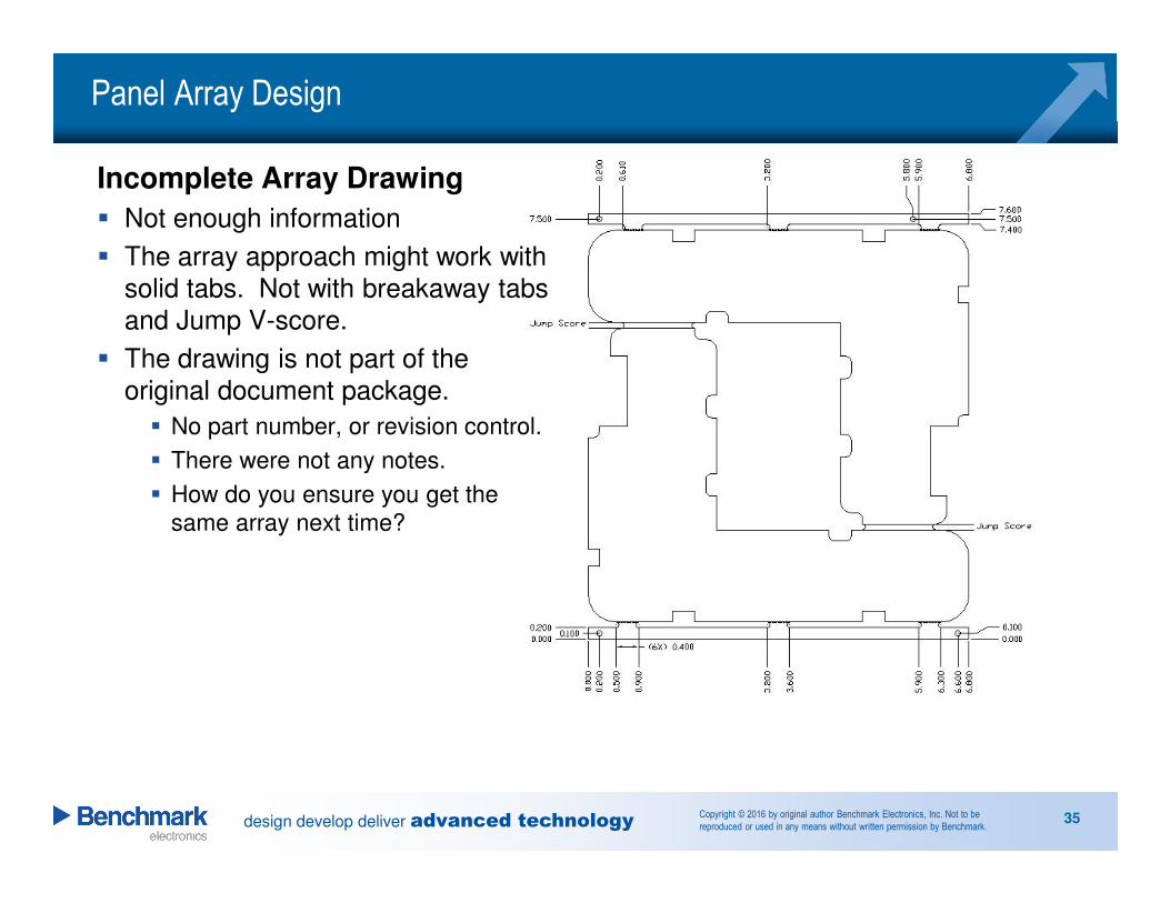
Incomplete Array Drawing
� Not enough information
� The array approach might work with
solid tabs. Not with breakaway tabs
and Jump V-score.
� The drawing is not part of the
original document package.
� No part number, or revision control.
� There were not any notes.
� How do you ensure you get the
same array next time?
Panel Array Design
design develop deliver advanced technologyCopyright © 2016 by original author Benchmark Electronics, Inc. Not to be
reproduced or used in any means without written permission by Benchmark.36
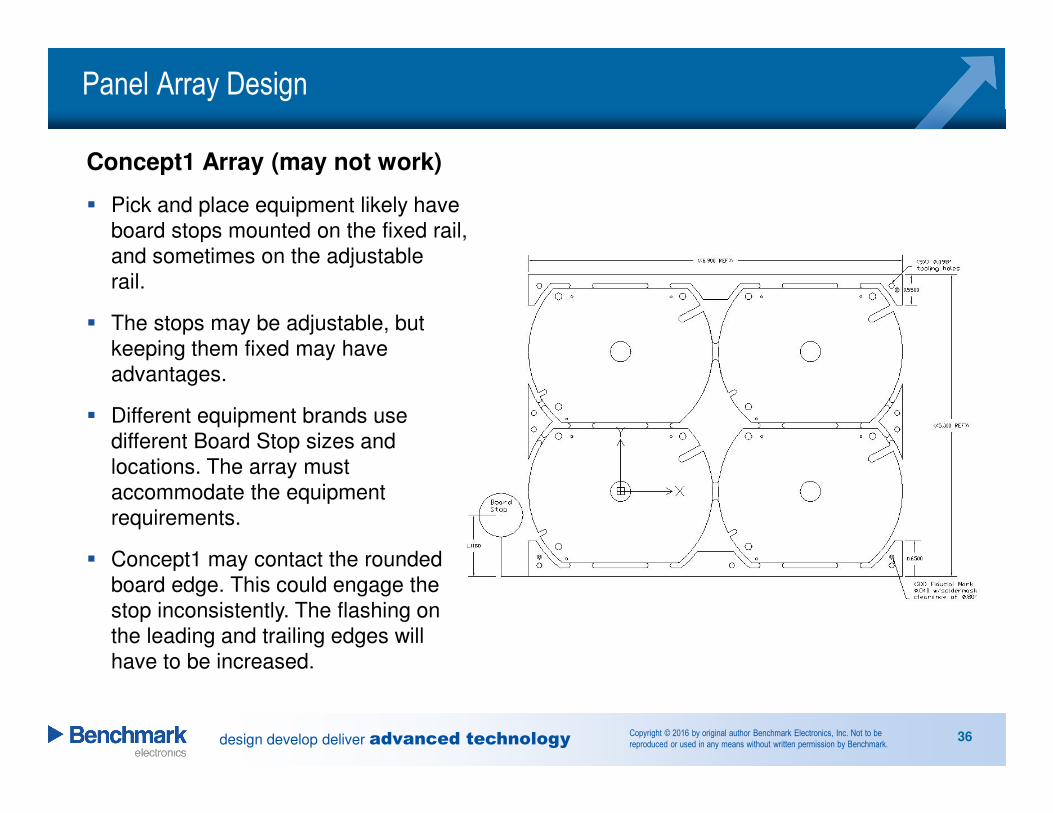
Concept1 Array (may not work)
� Pick and place equipment likely have
board stops mounted on the fixed rail,
and sometimes on the adjustable
rail.
� The stops may be adjustable, but
keeping them fixed may have
advantages.
� Different equipment brands use
different Board Stop sizes and
locations. The array must
accommodate the equipment
requirements.
� Concept1 may contact the rounded
board edge. This could engage the
stop inconsistently. The flashing on
the leading and trailing edges will
have to be increased.
Panel Array Design
design develop deliver advanced technologyCopyright © 2016 by original author Benchmark Electronics, Inc. Not to be
reproduced or used in any means without written permission by Benchmark.37
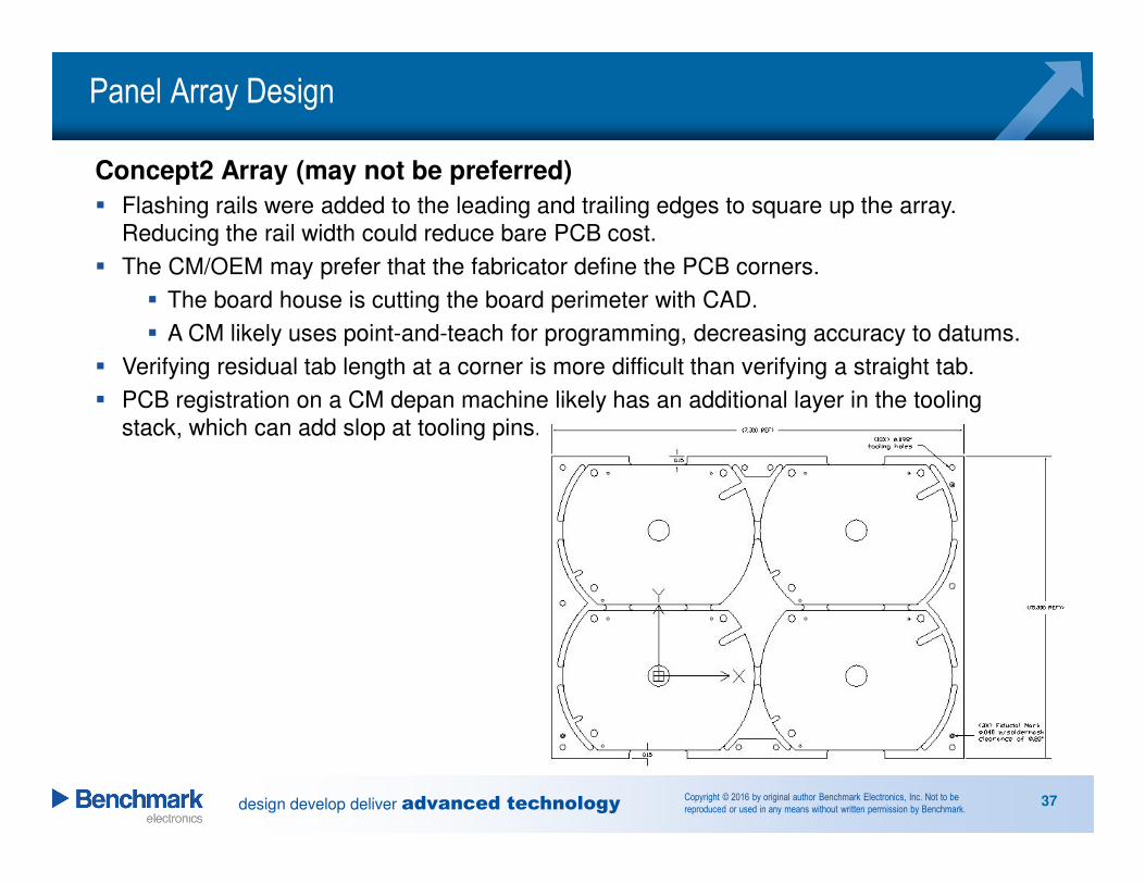
Concept2 Array (may not be preferred)
� Flashing rails were added to the leading and trailing edges to square up the array.
Reducing the rail width could reduce bare PCB cost.
� The CM/OEM may prefer that the fabricator define the PCB corners.
� The board house is cutting the board perimeter with CAD.
� A CM likely uses point-and-teach for programming, decreasing accuracy to datums.
� Verifying residual tab length at a corner is more difficult than verifying a straight tab.
� PCB registration on a CM depan machine likely has an additional layer in the tooling
stack, which can add slop at tooling pins.
Panel Array Design

design develop deliver advanced technologyCopyright © 2016 by original author Benchmark Electronics, Inc. Not to be
reproduced or used in any means without written permission by Benchmark.38
Concept3 Array (works)
� A full frame around the board was used in this instance. The rails were made no
wider than necessary to support the 4-up configuration. With the addition of rails:
� SMT components must be at least 0.208mm (5.2mm) from array corners.
� The center of PCB fiducials must be at least 0.25” (6.4mm) from corners of array edges.
� At least (2) non plated tooling holes are provided within each piece of flashing.
� The individual board has at least two, usable fiducials on each side of the PCB in an asymmetrical pattern.
� An offset of 0.2” (5mm) will ensure a fiducial camera will not accidently read a fiducial of a PCB if loaded backwards, or upside down into a machine.
Panel Array Design
� The hole patterns were made asymmetrical, so
an array cannot be loaded into a fixture
backwards, or upside down. (Prefer if this offset is
visually obvious.)
� Three array fiducials were provided.

design develop deliver advanced technologyCopyright © 2016 by original author Benchmark Electronics, Inc. Not to be
reproduced or used in any means without written permission by Benchmark.39
Concept3 Array (Dimensions)
� Page 2 of Fab Drawing
� PCB origin
� Array origin
� Tab locations
� Fiducial size and location.
� Tooling hole size and location.
� Overall dimension shown as a reference.
� Tooling holes center to center with
tolerance.
Some dimensions have been removed for clarity.
Panel Array Design
design develop deliver advanced technologyCopyright © 2016 by original author Benchmark Electronics, Inc. Not to be
reproduced or used in any means without written permission by Benchmark.40
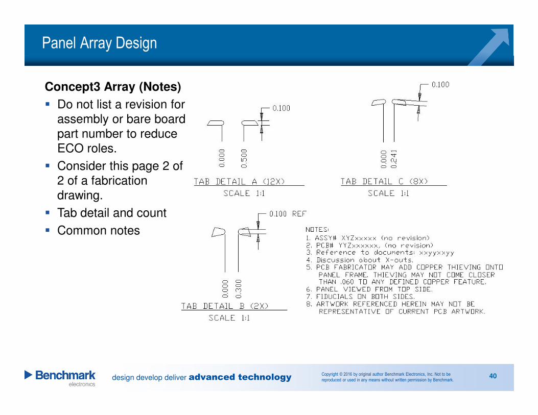
Concept3 Array (Notes)
� Do not list a revision for
assembly or bare board
part number to reduce
ECO roles.
� Consider this page 2 of
2 of a fabrication
drawing.
� Tab detail and count
� Common notes
Panel Array Design
design develop deliver advanced technologyCopyright © 2016 by original author Benchmark Electronics, Inc. Not to be
reproduced or used in any means without written permission by Benchmark.41
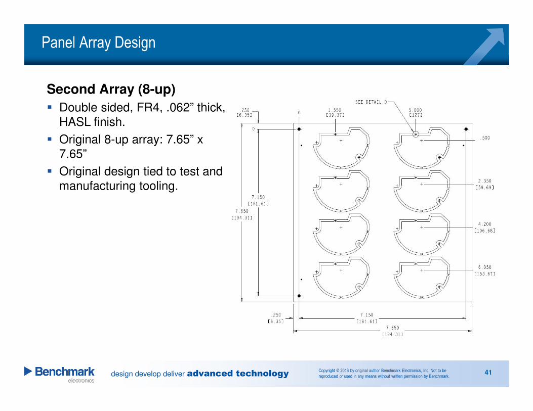
Second Array (8-up)
� Double sided, FR4, .062” thick,
HASL finish.
� Original 8-up array: 7.65” x
7.65”
� Original design tied to test and
manufacturing tooling.
Panel Array Design
design develop deliver advanced technologyCopyright © 2016 by original author Benchmark Electronics, Inc. Not to be
reproduced or used in any means without written permission by Benchmark.42
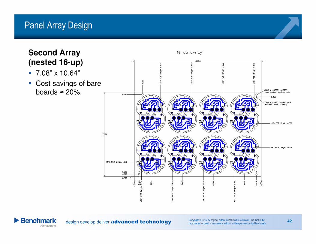
Second Array (nested 16-up)
� 7.08” x 10.64”
� Cost savings of bare
boards ≈ 20%.
Panel Array Design
design develop deliver advanced technologyCopyright © 2016 by original author Benchmark Electronics, Inc. Not to be
reproduced or used in any means without written permission by Benchmark.43
IPC 4101 Laminate Materials
/126 or /130
� In no order of preference suggested materials that meet /126 are:
1. ITEQ IT-180A, IT-175GRA
2. Panasonic 1755V
3. Nelco N4000-29, N4800-20
4. Hitachi E-679F, E-679 (W)
5. Isola 370HR, 185HR, I-Speed
� IPC 4101 /130 criteria must be met for product requiring Halogen free
construction. In no order of preference suggested materials are: TUC TU-
862 HF and Hitachi E75G.
design develop deliver advanced technologyCopyright © 2016 by original author Benchmark Electronics, Inc. Not to be
reproduced or used in any means without written permission by Benchmark.44
IPC 4101 Laminate Materials
� Alternate laminate materials must be approved prior to substitution or use.
� All laminates must have cross linking agents that will assure successful lead
free assembly; having superior CAF resistance and IST test results.
� Laminate must survive 6 cycles of 288°C solder float test. Each solder float
test duration equals 10 seconds. Material and hole integrity must be
maintained.
� Laminate must survive 6 simulated re-flow cycles that include a 260°C peak
maintained for at least 20 seconds. Material shall not show signs of
blistering.
� Laminate glass transition temperature (Tg) shall be rated at minimum of 170
°C and shall pass UL laminate Test T-260 for 30 minutes minimum (260°C)
and T-288 for 4 minutes (288°C) per IPC-TM-650 2.4.24.1 on fabricated
PCB. The average Tg should be Nominal ±5°C.
design develop deliver advanced technologyCopyright © 2016 by original author Benchmark Electronics, Inc. Not to be
reproduced or used in any means without written permission by Benchmark.45
IPC 4101 Laminate Materials
See IPC-4101 for differences between /126 and /129 laminates.
� /126 materials may be more robust than /129 materials for RoHS applications
� /129 materials may be suitable for some RoHS applications.
� /129 has a higher Z-Axis CTE from 50 to 260°C than /126. This should be
considered when choosing materials for thicker substrates.
design develop deliver advanced technologyCopyright © 2016 by original author Benchmark Electronics, Inc. Not to be
reproduced or used in any means without written permission by Benchmark.46
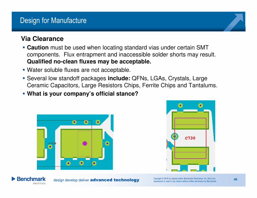
Via Clearance
� Caution must be used when locating standard vias under certain SMT
components. Flux entrapment and inaccessible solder shorts may result.
Qualified no-clean fluxes may be acceptable.
� Water soluble fluxes are not acceptable.
� Several low standoff packages include: QFNs, LGAs, Crystals, Large
Ceramic Capacitors, Large Resistors Chips, Ferrite Chips and Tantalums.
� What is your company’s official stance?
Design for Manufacture
design develop deliver advanced technologyCopyright © 2016 by original author Benchmark Electronics, Inc. Not to be
reproduced or used in any means without written permission by Benchmark.47
Copper Plating Fabrication Note
The printed circuit board must meet:
A) (Default requirements) IPC – 6012 Class 2 performance requirements except:
� The minimum average copper thickness in all plated through holes shall be 25.4 µm
(1.0 mil) with the minimum measurement of at least 20.3 µm (0.8 mils).
� The minimum copper thickness in the barrel of blind and buried vias shall be 20.3 µm
(0.8mils).
� The minimum internal annular ring must be 25.4 µm (0.001”) at land / conductor
junction, and tangency elsewhere.
� The minimum external annular ring must be 50.8 µm (0.002”) at land conductor
junction, and 25.4 µm (0.001”) elsewhere.
B) (more strict requirements) IPC – 6012 Class 3 performance requirements.
Design for Manufacture
design develop deliver advanced technologyCopyright © 2016 by original author Benchmark Electronics, Inc. Not to be
reproduced or used in any means without written permission by Benchmark.48
Hole diameter specifications:
Shall be listed on drill chart
� Finished hole diameters are measured after plating and any surface finish.
� Via with a FHS ≤ 0.5mm (0.020”) do not have a minimum hole size
requirement; however the via holes may not be closed by copper plate.
� Press-fit FHS diameter tolerance is ± 50.8 µm (0.002”).
� Holes > 5.6 mm (0.220”) may be nibble drilled, or routed and have a
tolerance ± 0.127mm (0.005”).
� Non-plated tooling-hole diameter tolerance is ± 50.8 µm (0.002”).
� All remaining FHS tolerances are ± 75 µm (0.003”).
Design for Manufacture
design develop deliver advanced technologyCopyright © 2016 by original author Benchmark Electronics, Inc. Not to be
reproduced or used in any means without written permission by Benchmark.49
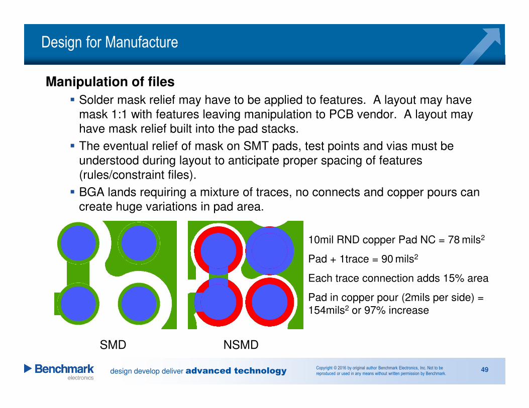
Manipulation of files
� Solder mask relief may have to be applied to features. A layout may have
mask 1:1 with features leaving manipulation to PCB vendor. A layout may
have mask relief built into the pad stacks.
� The eventual relief of mask on SMT pads, test points and vias must be
understood during layout to anticipate proper spacing of features
(rules/constraint files).
� BGA lands requiring a mixture of traces, no connects and copper pours can
create huge variations in pad area.
SMD NSMD
10mil RND copper Pad NC = 78 mils2
Pad + 1trace = 90 mils2
Each trace connection adds 15% area
Pad in copper pour (2mils per side) =
154mils2 or 97% increase
Design for Manufacture
design develop deliver advanced technologyCopyright © 2016 by original author Benchmark Electronics, Inc. Not to be
reproduced or used in any means without written permission by Benchmark.50
Manipulation of files
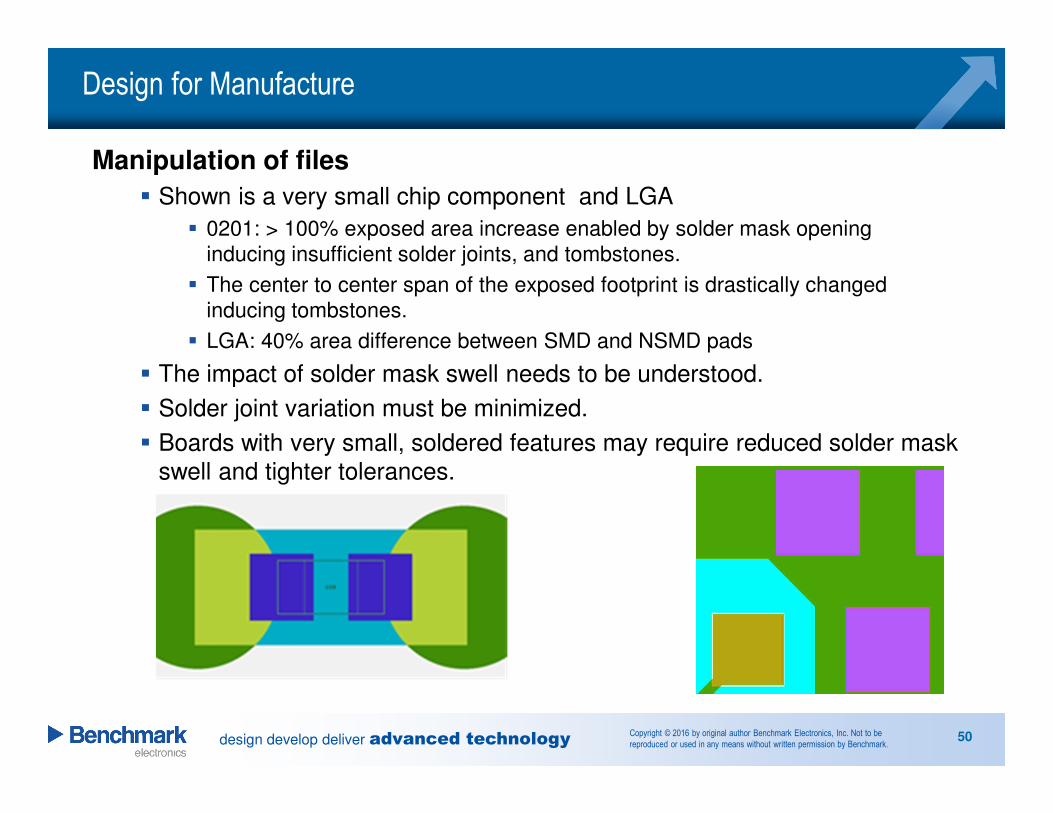
� Shown is a very small chip component and LGA
� 0201: > 100% exposed area increase enabled by solder mask opening
inducing insufficient solder joints, and tombstones.
� The center to center span of the exposed footprint is drastically changed
inducing tombstones.
� LGA: 40% area difference between SMD and NSMD pads
� The impact of solder mask swell needs to be understood.
� Solder joint variation must be minimized.
� Boards with very small, soldered features may require reduced solder mask
swell and tighter tolerances.
Design for Manufacture
design develop deliver advanced technologyCopyright © 2016 by original author Benchmark Electronics, Inc. Not to be
reproduced or used in any means without written permission by Benchmark.51
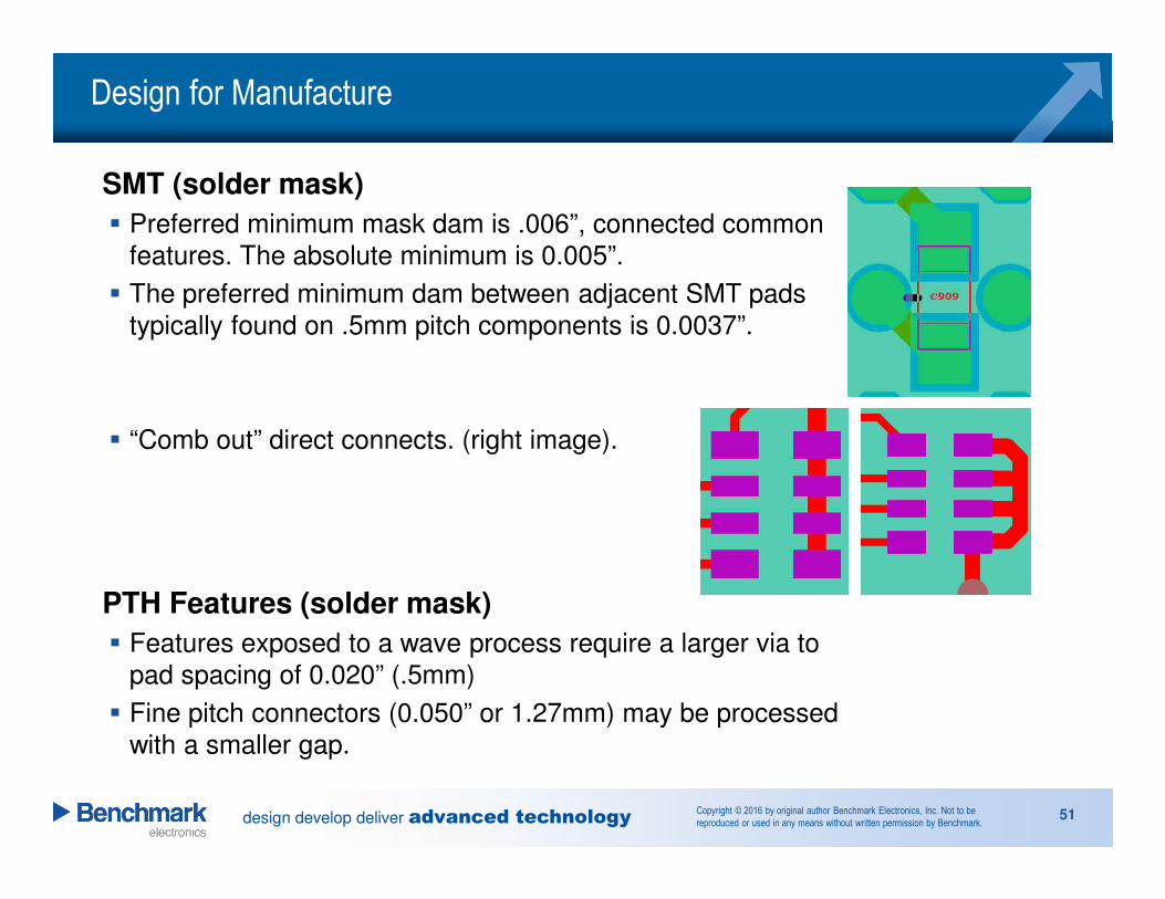
SMT (solder mask)
� Preferred minimum mask dam is .006”, connected common
features. The absolute minimum is 0.005”.
� The preferred minimum dam between adjacent SMT pads
typically found on .5mm pitch components is 0.0037”.
� “Comb out” direct connects. (right image).
PTH Features (solder mask)
� Features exposed to a wave process require a larger via to
pad spacing of 0.020” (.5mm)
� Fine pitch connectors (0.050” or 1.27mm) may be processed
with a smaller gap.
Design for Manufacture
design develop deliver advanced technologyCopyright © 2016 by original author Benchmark Electronics, Inc. Not to be
reproduced or used in any means without written permission by Benchmark.52
PWB Design Considerationsmpedance
� Conductor to Board Edge Spacing
� 0.5mm (0.020”) Minimum
� 1.27mm (0.050”) Preferred
� For board edges without flashing, we prefer 1.27mm (0.050”)
copper to board edge clearance to prevent handling damage.
� Conductor to board cut-out spacing is the same as conductor to board edge spacing.
Design for Manufacture
design develop deliver advanced technologyCopyright © 2016 by original author Benchmark Electronics, Inc. Not to be
reproduced or used in any means without written permission by Benchmark.53
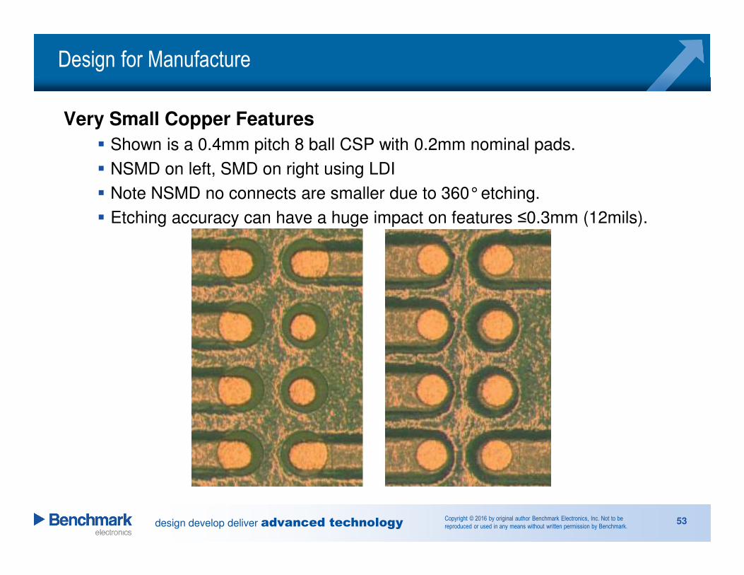
Very Small Copper Features
� Shown is a 0.4mm pitch 8 ball CSP with 0.2mm nominal pads.
� NSMD on left, SMD on right using LDI
� Note NSMD no connects are smaller due to 360°etching.
� Etching accuracy can have a huge impact on features ≤0.3mm (12mils).
Design for Manufacture
design develop deliver advanced technologyCopyright © 2016 by original author Benchmark Electronics, Inc. Not to be
reproduced or used in any means without written permission by Benchmark.54
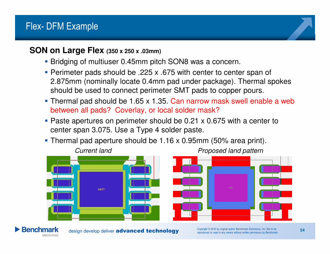
SON on Large Flex (350 x 250 x .03mm)
� Bridging of multiuser 0.45mm pitch SON8 was a concern.
� Perimeter pads should be .225 x .675 with center to center span of
2.875mm (nominally locate 0.4mm pad under package). Thermal spokes
should be used to connect perimeter SMT pads to copper pours.
� Thermal pad should be 1.65 x 1.35. Can narrow mask swell enable a web
between all pads? Coverlay, or local solder mask?
� Paste apertures on perimeter should be 0.21 x 0.675 with a center to
center span 3.075. Use a Type 4 solder paste.
� Thermal pad aperture should be 1.16 x 0.95mm (50% area print).
Current land Proposed land pattern
Flex- DFM Example
design develop deliver advanced technologyCopyright © 2016 by original author Benchmark Electronics, Inc. Not to be
reproduced or used in any means without written permission by Benchmark.55
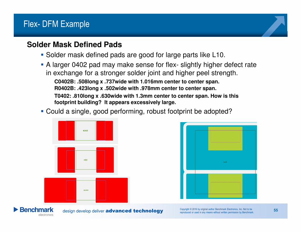
Solder Mask Defined Pads
� Solder mask defined pads are good for large parts like L10.
� A larger 0402 pad may make sense for flex- slightly higher defect rate
in exchange for a stronger solder joint and higher peel strength.
C0402B: .508long x .737wide with 1.016mm center to center span.
R0402B: .423long x .502wide with .978mm center to center span.
T0402: .810long x .630wide with 1.3mm center to center span. How is this footprint building? It appears excessively large.
� Could a single, good performing, robust footprint be adopted?
Flex- DFM Example
design develop deliver advanced technologyCopyright © 2016 by original author Benchmark Electronics, Inc. Not to be
reproduced or used in any means without written permission by Benchmark.56
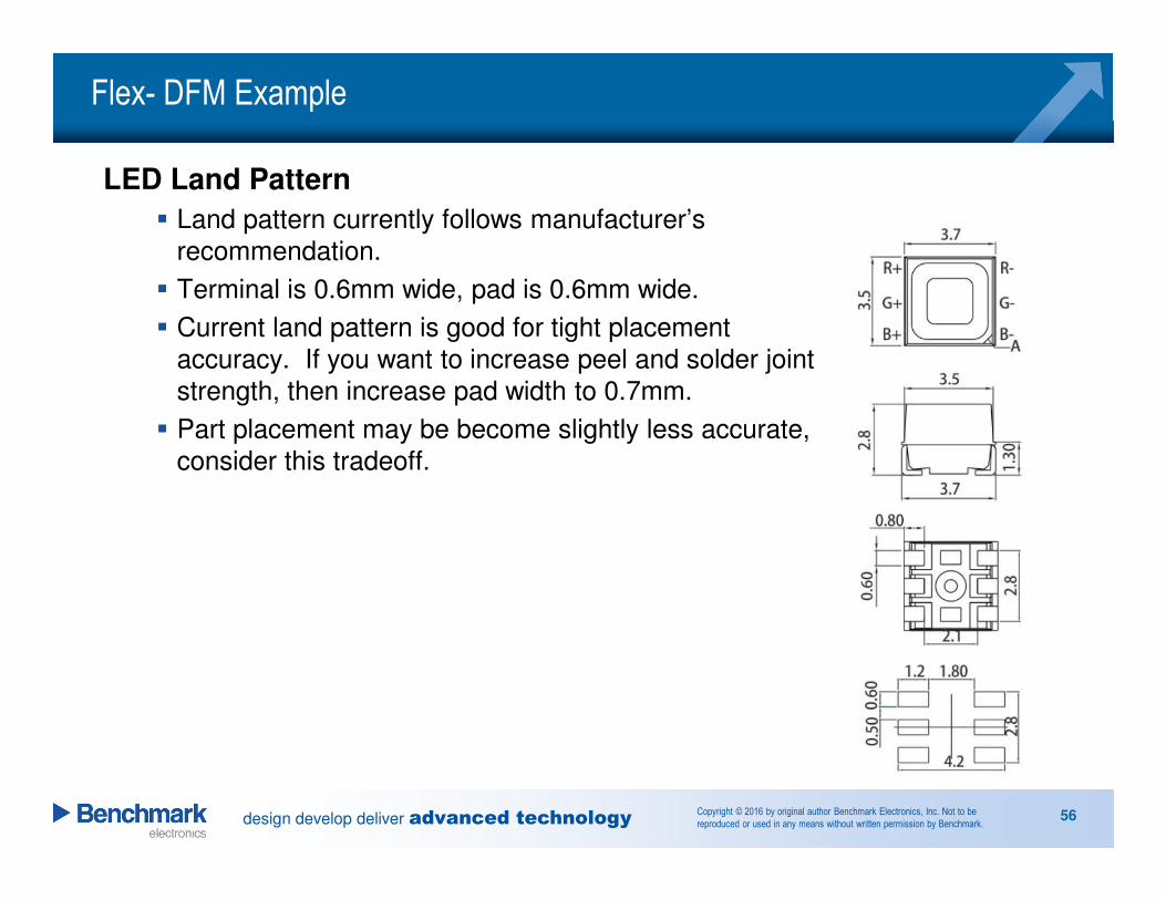
LED Land Pattern
� Land pattern currently follows manufacturer’s
recommendation.
� Terminal is 0.6mm wide, pad is 0.6mm wide.
� Current land pattern is good for tight placement
accuracy. If you want to increase peel and solder joint
strength, then increase pad width to 0.7mm.
� Part placement may be become slightly less accurate,
consider this tradeoff.
Flex- DFM Example
design develop deliver advanced technologyCopyright © 2016 by original author Benchmark Electronics, Inc. Not to be
reproduced or used in any means without written permission by Benchmark.57
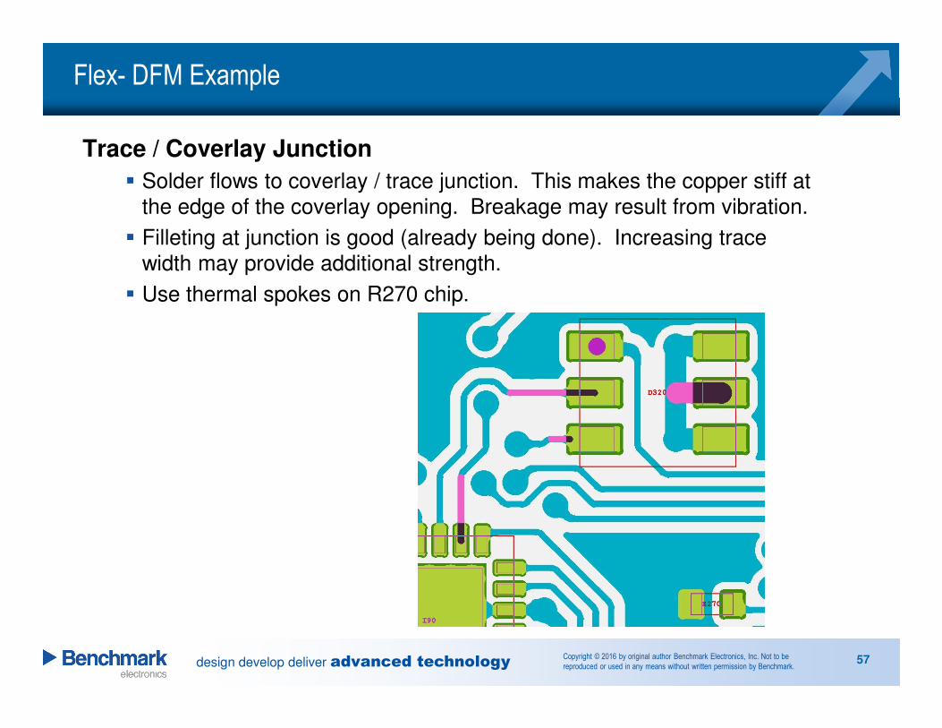
Trace / Coverlay Junction
� Solder flows to coverlay / trace junction. This makes the copper stiff at
the edge of the coverlay opening. Breakage may result from vibration.
� Filleting at junction is good (already being done). Increasing trace
width may provide additional strength.
� Use thermal spokes on R270 chip.
Flex- DFM Example
design develop deliver advanced technologyCopyright © 2016 by original author Benchmark Electronics, Inc. Not to be
reproduced or used in any means without written permission by Benchmark.58
Design for Manufacture
Thank you for taking the time to visit Benchmark Electronics.
Please have safe travels.