design methodology for mfb filters in adc interface ... · design methodology for mfb filters in...
TRANSCRIPT

Application ReportSBOA114–February 2006
Design Methodology for MFB Filters in ADC InterfaceApplications
Michael Steffes.................................................................................................... High-Speed Products
ABSTRACTWhile the Multiple FeedBack (MFB) filter topology is well-known, its application to veryhigh dynamic range analog-to-digital converter (ADC) interfaces requires a carefulconsideration of component value selection. This application report develops the idealtransfer function, then introduces a component selection methodology and discusses itsimpact on noise and distortion. The impact of amplifier Gain Bandwidth Product on finalpole locations is also included, showing several examples. A complete high dynamicrange, differential I/O filter for wide dynamic range ADC driving is then designed. Asimple design spreadsheet embodying this design approach is available for downloadwith this application report.
Contents1 MFB Filter Transfer Function...................................................................... 22 MFB Active Filter Noise Gain Analysis .......................................................... 53 Setting the Integrator Pole to Improve Noise and Distortion.................................. 74 Example Designs Showing the Impact of Integrator Pole Location.......................... 85 MFB Filter Implemented with Non-Unity-Gain Stable Op Amps ........................... 126 Differential Version of 3rd-Order Design ....................................................... 157 Pole Sensitivity to Amplifier Gain Bandwidth Product ........................................ 178 Summary ........................................................................................... 209 References......................................................................................... 20Appendix A Output Noise Analysis .................................................................. 21Appendix B Solution for R3 and C1 .................................................................. 23Appendix C Effect of an Equal C Target ............................................................ 26Appendix D Noise Gain Zeroes with C1 = ∞ ........................................................ 27Appendix E Noise Gain Zeroes for R3 = R2 Targeted ............................................. 30
List of Figures
1 MFB Filter Topology................................................................................ 22 DC Analysis Circuit ................................................................................. 33 Feedback Analysis Circuit for MFB Filter........................................................ 64 Initial Test Circuit using the OPA820 in a 1MHz, Butterworth Low-Pass Filter
Configuration ........................................................................................ 95 Noise Gain and Open-Loop Gain for Circuit in Figure 4 ...................................... 96 New Design Circuit with Noise Gain Peaking ................................................. 107 Noise Gain Plot for Figure 6 ..................................................................... 108 Simulated Small Signal Bandwidth for Figure 4 and Figure 6............................... 119 Output Spot Noise Comparison ................................................................. 1210 Noise Gain Plot for Initial OPA2614 MFB Filter Design...................................... 1311 Noise Gain with OPA2614 Open-Loop Gain for CT = 31.8pF ............................... 1412 Frequency Response for the OPA2614 MFB Filter Design (Each 1/2 of Figure 14)..... 1413 Expanded View of 3rd-Order Filter Response (see Figure 14) ............................. 1514 Single-Supply Differential ADC Interface with 3rd-Order Bessel Filter (with f-3dB =
FilterPro is a trademark of Texas Instruments.All trademarks are the property of their respective owners.
SBOA114–February 2006 Design Methodology for MFB Filters in ADC Interface Applications 1Submit Documentation Feedback

www.ti.com
1 MFB Filter Transfer Function
R1
R3
R2
C1
C2
VO
VI
VFB
MFB Filter Transfer Function
5MHz)............................................................................................... 1615 OPA2614 Single +5V Distortion for Noninverting Differential Gain of 8 ................... 17A-1 Noise Analysis Circuit for MFB Filter ........................................................... 21
The Multiple FeedBack (MFB) filter is widely used for very high dynamic range ADC input stages. Thisfilter offers exceptional stop band rejection over other filter topologies (Ref. 1). Figure 1 shows the startingpoint for this filter design.
Figure 1. MFB Filter Topology
This design is an inverting signal path, 2nd-order, low-pass filter that offers numerous advantages overSallen-Key filters. This single-ended I/O interface can be easily adapted to a differential I/O interface, aswill be shown later.
A few of the advantages of this topology include:
1. No gain for the noninverting current noise and/or DC bias current. Figure 1 shows the non-invertinginput grounded, which is great for reducing noise but less than ideal for DC precision. Adding a resistorequal to the DC impedance looking out the inverting node achieves bias current cancellation; adding acapacitor across this resistor reduces the noise contribution for the resistor and the op amp biascurrent noise. If the amplifier is a JFET or CMOS type, this bias current cancellation will not work andthe noninverting input should simply be set to ground or a desired reference voltage.
2. The in-band signal gain is set by – (R1/R3). As will be shown, R3 also sets the Q of the filter whilehaving no influence over ωo.
Embedded within the filter is an Integrator comprised of R2 and C2, along with the Voltage FeedBack(VFB) op amp. This design normally needs to be implemented using a unity-gain stable, VFB op ampbecause the core gain element needs to be configured as an Integrator. There are dynamic rangeadvantages to using non-unity-gain stable VFB amplifiers and a design approach for successfully applyingthose types of devices will be shown later. However, a Current FeedBack (CFB) op amp is usually notsuitable to this type of filter since its local stability requires a feedback resistor nearly equal to arecommended value. A capacitive feedback as required in Figure 1 will typically not work with CFB ampswithout some design tricks that usually impair noise performance (Ref. 2). Since the emerging FullyDifferential Amplifiers (FDA) are essentially voltage feedback op amps, they can also be applied quitesuccessfully to this topology (Ref. 3).
Numerous approaches to selecting the component values are available in the literature (see, for example,Ref. 4). An equal-R approach is common, and will be shown as a desirable approach once an initial R2 ischosen. As ADCs continue to improve, the resistor noise in this filter can actually be a dominant elementin the total noise spectrum delivered to the converter input. One outcome of the equal-R design (Ref. 4) isthat quite unequal Cs are then required for most filter targets. That is in fact generally true for this filtertype (as will be shown later). If an equal C design is desired, another filter type should be considered(Sallen-Key).
2 Design Methodology for MFB Filters in ADC Interface Applications SBOA114–February 2006Submit Documentation Feedback

www.ti.com
Vo
V i 1
C1C2R2R3· 1
s2s 1C1R2R3
R3R21R3
R1 1
R1R2C1C2 (1)
AVDC R1
R3
in VV(2)
o 1
R1R2C1C2 in radians
(3)
Q
C1C2
R1
R2
R2
R1
R1R2
R3
unitless
(4)
Or, with R1
R2,
Q R3
C1C2
R2
R3 1
(5)
RP
Set: = +R R R RP 2 1 3
úú
R2
R3
VO
VI
R1
MFB Filter Transfer Function
The Laplace transfer function for the circuit of Figure 1 is shown as Equation 1.
The various design goals of interest in this equation can be solved as:
• the DC gain (where s = 0):
• characteristic frequency:
• the quality factor:
As is usually the case in active filter design, there are more passive elements to be resolved than filtercharacteristics. Here, there are five elements and only three targets. This situation often leads to the verycommon equal-R assumption to reach a design where that is a somewhat arbitrary way to eliminate onedegree of freedom. There should be a more rational way to select component values for these filters.
Looking at the circuit of Figure 1 at DC gives the simplified circuit of Figure 2 that will be used to show theDC part of the low-pass filter.
Figure 2. DC Analysis Circuit
A resistor (RP) has been added on the noninverting input to provide for DC bias current cancellation in theoutput offset voltage. Setting it as shown reduces the output DC error to (IOS • R1) if the op amp shows aninput bias current that has an offset current specification. Again, JFET or CMOS amplifiers would not usethis RP resistor for output DC error reduction.
SBOA114–February 2006 Design Methodology for MFB Filters in ADC Interface Applications 3Submit Documentation Feedback

www.ti.com
eo (en)21
R1
R32
4kTR21R1
R32
4kTR11R1
R3in
2R21R1
R3R1
2(6)
1R1
R3
2
en2 4kTR2inR2
21R1
R3
2
in22R2R11
R1R3
(7)
R22R2 1AV
13AV 4kT
(in2) 1AV
13AVen
in
2
0(8)
R2 1AV
13AV 2kT
(in2)
113AV
1AV en
2kT2 1
(9)
C1 Q
oR21QoR2C21AV (10)
oR2C2 1
Q1AVfor C1 0
(11)
1oR2C2
Q1AV ratio of Integrator pole to target o(12)
MFB Filter Transfer Function
The total output noise is a considerably more involved discussion. Appendix A develops that expressionfor the circuit of Figure 2, where the bandlimiting effects of the filter capacitors are neglected. The totaloutput noise is given as Equation 6 (which is also Equation A-3 in Appendix A), where the terms arisingfrom RP are neglected.
It would be reasonable to assume that most designs would not want the resistor terms to add too muchmore noise at the output than the op amp noise voltage itself. This idea can be used to developEquation 7 (Equation A-4 in Appendix A) where the op amp noise voltage (squared) is targeted to beequal to the total noise power contribution of the R2 and R3 resistors at the output.
This expression still includes both R1 and R3. R3 is also a resistor that will contribute to the total outputnoise in a similar fashion to R2. It would be preferable to make it as low as possible within the constraintthat it should not load the driving signal source to the point of creating a dominant distortion mechanism inthat prior stage. As a maximum value, it might be reasonable to let it equal R2 while recognizing thatmoving it lower will benefit the total output noise. If R3 is tentatively set equal to R2, Equation 7 can besimplified and put into a form to solve for R2, as shown in Equation 8 (from Equation A-13 in Appendix A).
This equation may then be solved using the quadratic equation for an initial target value for R2 as shownin Equation 9 (where only the positive solution for R2 is used; note that Equation 9 is also Equation A-14 inAppendix A).
This formula gives an initial suggested value for R2 (note that embedded in this solution is the assumptionthat R3 will then be set equal to R2). Both R2 and R3 may be set lower to improve noise. Recognize,however, that very low values will start to load the output stage driving into this filter and the filter op ampoutput stage (if R1 is also very low). They can also be set higher to lighten the loading where an increasein total output noise will be the result.
Once R2 is selected, either from this noise consideration or from some other approach, we now need toselect one of the capacitor values to remove it from the filter design equations. With two elementsselected, the remaining three can be used to set the three filter design goals. In solving to achieve thedesired filter shape, it is possible (Appendix B) to arrive at an equation for C1 that shows a criticalconstraint on the R2C2 product. That constraint can be seen in Equation 10 (which is taken fromAppendix B as Equation B-22):
Equation 10 clearly shows that the R2C2 product must be low enough to keep the solution for C1 > 0. Thatconstraint is shown as Equation 11:
or:
4 Design Methodology for MFB Filters in ADC Interface Applications SBOA114–February 2006Submit Documentation Feedback

www.ti.com
C22 C2
1R2Qo 1AV
1
(R2o)21AV
0(13)
C2 1
2QR2o1AV1 1(2Q)2(1AV)
(14)
C2 C1 1
1.43R2o (15)
2 MFB Active Filter Noise Gain Analysis
MFB Active Filter Noise Gain Analysis
(1 / ωoR2C2) is physically the ratio of the Integrator pole to the target ωo. Equation 12 sets a minimum limitfor that ratio, while moving above that limit is essentially moving the Integrator pole out relative to ωo(reducing C2 if ωo and R2 are fixed). Solving for equality in Equation 12 solves for an infinite value of C1.So, moving the Integrator pole out also reduces the required value for C1 from infinity to some morereasonable value.
While Equation 11 and Equation 12 give a nice limit on a solution for C2 and C1 (note that once C2 isselected, Equation 10 gives C1 completely defined by the desired filter shape and a selected R2 value),they do not tell us much about where to place the Integrator pole.
One option considered for many active filter designs is to set the two capacitors equal. This solution issometimes considered preferable to get better matching in order to minimize the sensitivity functions.Equation 10 actually gives us an easy way to test this approach by temporarily targeting C1 = C2, thensolving the resulting expression for C2 (Appendix C). Equation 13 shows the resulting quadratic whileEquation 14 shows the solution for C2. Again, this simplified approach is only possible if R2 is initiallyselected from either a noise approach or some other consideration.
(which is Equation C-3 in Appendix C;)
(which is Equation C-10 in Appendix C;)
The radical in Equation 14 only solves for non-imaginary C2 values if (2Q)2 • (1 + AV) ≤ 1. Assuming aminimum AV = 1 requires a Q < 0.353. Setting Q = 0.353 and AV = 1 gives a C2 solution that is tworepeated values given in Equation 15:
Using an active filter for a Q < 0.5 (two real poles) and/or gain < 1 is unlikely because a simple passivecircuit can easily provide attenuation and two real poles without requiring an active element. Thus, anequal C design is interesting but not particularly useful for an MFB filter design.
One possible approach to setting the (1 / R2C2) product (Integrator pole location) is to investigate whatimpact it might have on the resulting noise gain for the completed filter. Recall that the noise gain is thereciprocal of the feedback attenuation from the op amp output pin back to the inverting input pin. Thisnoise gain is an important consideration for at least three reasons.
1. Any peaking in the noise gain will, of course, peak up the gain to the output for the total equivalentinput voltage noise (including the R2 effects considered earlier).
2. Noise gain peaking will also reduce the loop gain. All other things being equal, reduced loop gain willshow up as higher output harmonic distortion.
3. The point where the noise gain crosses the open-loop gain (in a Bode plot) also determines the loopgain phase margin. Phase margin at this crossover point sets the stability for the overall design.
The feedback divider circuit for the MFB filter is shown in Figure 3. An added element is included here thatwas not in Figure 1—a parasitic or intentional capacitor (CT) on the inverting input pin.
SBOA114–February 2006 Design Methodology for MFB Filters in ADC Interface Applications 5Submit Documentation Feedback

www.ti.com
R2V–
C2
VO
R1
CT C1 R3
Source input, assumed
low impedance.
V
VO
C2CT C2
·
s2s 1C1R3
1C1 R1R2
1R1R2C1C2
s2s 1C1R3
1C1 R1R2
1R2 CTC2
1R2 R1R3C1 CTC2 (16)
1 1
CTC2·
s2s 1C1R3
1C1 R1R2
1R2 CTC2
1R2 R1R3C1 CTC2
s2s 1C1R3
1C1 R1R2
1R1R2C1C2
(17)
1
s2s 1C1R3
1C1
R1R2
1R2C2 1
R2R1R3
C1C2
s2s 1C1R3
1C1
R1R2 1
R1R2C1C2(18)
MFB Active Filter Noise Gain Analysis
Figure 3. Feedback Analysis Circuit for MFB Filter
Here, it is easy to see the multiple feedback nature of the circuit. At DC, the path is through R1 and R2,while at high frequencies it is through C2.
The desired Laplace transfer function here is from VO to V– (the inverting input voltage). This attenuator isnormally referred to as the β in control theory discussions of negative feedback systems. The solution forβ is shown as Equation 16.
We are normally more interested in looking at 1 / β, which will be the noise gain discussed earlier.
Inverting Equation 16 gives Equation 17.
There are several key points to Equation 17:
1. The poles are identical to the desired filter poles.2. The DC (s = 0) gain becomes (1 + R1/R3).3. The high frequency gain (as s→∞) goes to (1 + CT/C2).4. If CT << C2, then the high frequency noise gain approaches 1.
The noise gain transfer function has two zeroes and two poles. The transition between the DC gain andhigh frequency gain depends on the relative position of the zeroes and poles. It would be preferable tominimize the peaking in the noise gain within the desired low-pass frequency band as it makes thistransition from the DC gain to the s→∞ gain. If the desired filter shape calls for a high Q, peaking in thisnoise gain response is unavoidable as the frequency approaches ωo. If, however, one or both zeroes areplaced to fall below the ωo frequency, added noise gain peaking results that might be unnecessary. Thequestion then is whether or not those zeroes can be placed above ωo in order to limit any additionalin-band peaking for the noise gain.
Starting from Equation 17, first set CT = 0 for this portion of the analysis. It will be used later to allownon-unity-gain stable amplifiers to be used in the MFB topology, but will unnecessarily complicate theresolution of (1 / R2C2). Rewriting Equation 17 with this simplification yields Equation 18.
6 Design Methodology for MFB Filters in ADC Interface Applications SBOA114–February 2006Submit Documentation Feedback

www.ti.com
1
s2soQ 1
R2C21AVo
2
s2soQo
2MFB noise gain
(19)
3 Setting the Integrator Pole to Improve Noise and Distortion
QC Q 1AV
1Q21AV x
1x2 [where x Q 1AV ]
(20)
1oR2C2
Q2AV1 [where R3 R2 is desired ](21)
Z1 , 2 o
2Q1Q2 2AV1
1 1 2Q 1AV
1Q2(2AV1)
2
(22)
Setting the Integrator Pole to Improve Noise and Distortion
Then, observing that the numerator coefficients are very nearly the same as the denominator coefficients,we can rewrite the noise gain equation in terms of the desired filter characteristics as shown inEquation 19.
Here, it becomes very apparent that the embedded Integrator pole location, (1 / R2C2), is the one addeddegree of freedom in setting the noise gain zeroes. All of the other elements feeding into the noise gainzero coefficients are set by the desired low-pass, 2nd-order filter terms. It is therefore very useful to castthe design analysis in terms of this Integrator pole location. More specifically, working in terms of the ratio(1 / ωoR2C2) allows better simplification and is simply the ratio of the target characteristic frequency andthe embedded Integrator pole location.
One limit to the range on (1 / ωoR2C2) has already been set in Equation 12 to achieve real values for C1.Setting (1 / ωoR2C2) equal to Q (1 + AV) will solve C1 for infinity and R3 for zero. Neither of these valuesare particularly useful for implementation, but are interesting as a limit to the noise gain zero locations.Using Equation 12 to set a minimum level for 1 / R2C2 gives ωo • Q • (1 + AV). Putting this result into thenumerator of Equation 19, and solving for the equivalent QC for the zeroes of the noise gain in terms ofthe desired filter shape terms, gives Equation 20 (from Appendix D, Equation D-9).
This result is very useful in that it clearly shows the maximum possible value for QC is one-half. (1) Thisoccurs for any combination of desired AV and Q that sets Q • √(1 + Av) = 1. The most common conditionfor this would be Q = 0.707 (Butterworth target) and AV = 2. That combination, with a target for theIntegrator pole set by Equation 12, gives repeated real zeroes at ωo / Q (Appendix D). Several importantconclusions come from this combination.
1. The noise gain zeroes are always two real zeroes.2. They are repeated, and at the maximum value, at ωo / Q for the specific conditions described above
(which is not realizable since C1 = ∞).3. For Q > 1, it will necessarily be the case that one of the zeroes will fall below the target ωo. This
observation says that higher Q targets in the MFB filter have an added peaking in the noise gainbeyond just the desired filter pole peaking because one of the noise gain zeroes moves below ωo.
4. Moving the target (1 / ωoR2C2) up (moving the Integrator pole out) to get a real solution for C1effectively moves one of the zeroes up in frequency and the other down in frequency along thenegative real axis in the s-plane.
5. It turns out that this higher zero location corresponds very closely to 1 / R2C2 as the zeroes becomewidely separated.
As the (1 / ωoR2C2) target is increased from its minimum of Q • (1 + AV), C1 comes down from infinity andR3 increases from zero. These changes are both desirable within some limits. As R3 starts to increasebeyond the targeted R2 value (from the noise analysis of Equation 9), it will also start to add meaningfullyto the total output noise. One possible limit to R3 is to set it equal to R2 and resolve what this means for a(1 / ωoR2C2) target. Equation 21 shows this result (from Appendix E).
Appendix E goes on to solve for the resulting zero location if Equation 21 is used to set 1 / R2C2. Thatresult is shown as Equation 22 (Equation E-16 from Appendix E).
(1) x / (1 + x2) reaches a maximum value equal to 1/2 over 0 ≤ x ≤ ∞ at x = 1.
SBOA114–February 2006 Design Methodology for MFB Filters in ADC Interface Applications 7Submit Documentation Feedback
www.ti.com
QAV1 1
oR2C2 Q2AV1
(23)
Setting 1R2C2
oQ2AV1 gives R3 R2
while setting 1R2C2
oQAV1 gives C1 and R3 0(24)
4 Example Designs Showing the Impact of Integrator Pole Location
Example Designs Showing the Impact of Integrator Pole Location
Setting 1 / R2C2 as given in Equation 21 gets R3 = R2. It also sets the two noise gain zeroes as given byEquation 22. Moving the target (1 / ωoR2C2) below the value set by Equation 21 pulls the Integrator poledown, moves the lower zero to a higher frequency (acting to reduce the noise gain peaking), and reducesR3 below R2. All of these desirable effects suggest that (1 / ωoR2C2) should be set slightly below the valuedetermined by Equation 21 as long as the resulting R3 is not so low as to present too heavy a load for thedriving source into the filter. Since R3 in Figure 1 looks into a virtual ground node in-band, the inputimpedance below cutoff will be R3. Conversely, moving the (1 / ωoR2C2) above the value set byEquation 21 increases R3 beyond the targeted R2 value, moves the lower noise gain zero down further(causing added peaking in the noise gain within the desired frequency passband), and extends the highernoise gain zero out in frequency (approximating the 1 / R2C2 Integrator pole location).
In summary, the (1 / ωoR2C2) target should be set within the range indicated in Equation 23.
Now let's use these results to step through a design and observe the noise and distortion that results fromvarious selections of (1 / ωoR2C2). All of these designs give the desired filter shape. It is the noise gainshape and noise contributions of the resistor values that are of interest here.
Start with a target design given by:• ωo = 2π • 1MHz• Q = 0.707• AV = 2 (gives a negative gain of 2 for the signal path)
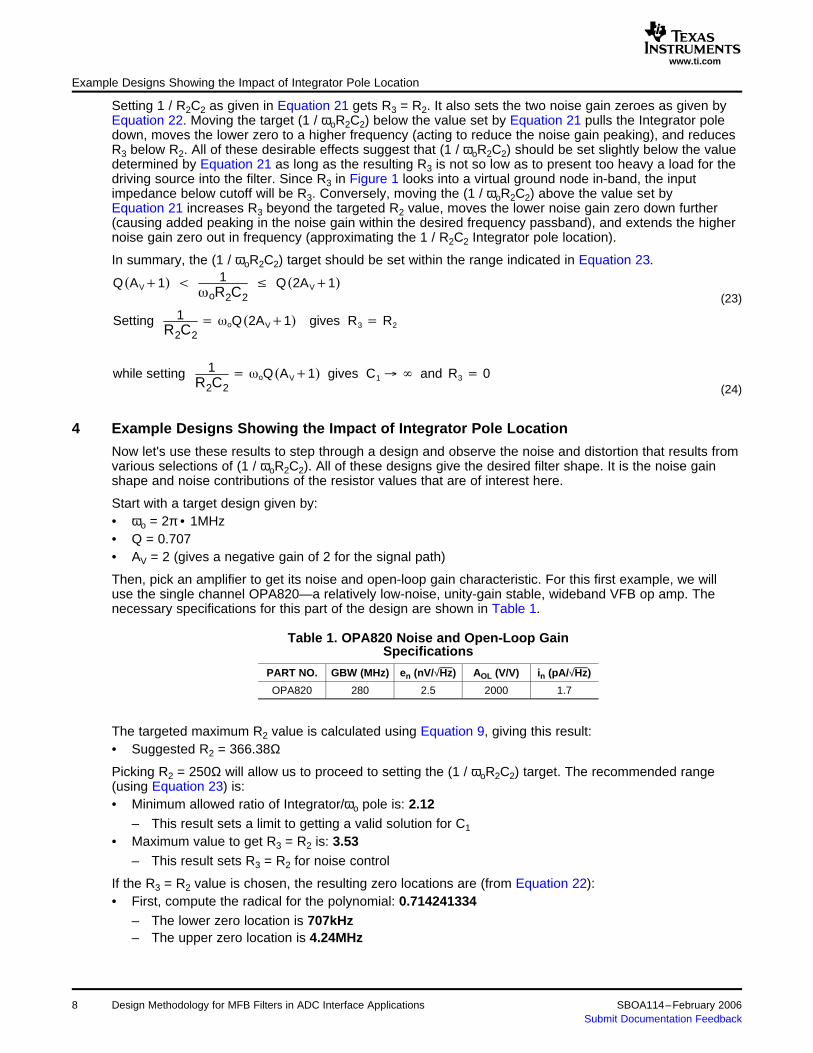
Then, pick an amplifier to get its noise and open-loop gain characteristic. For this first example, we willuse the single channel OPA820—a relatively low-noise, unity-gain stable, wideband VFB op amp. Thenecessary specifications for this part of the design are shown in Table 1.
Table 1. OPA820 Noise and Open-Loop GainSpecifications
PART NO. GBW (MHz) en (nV/√Hz) AOL (V/V) in (pA/√Hz)
OPA820 280 2.5 2000 1.7
The targeted maximum R2 value is calculated using Equation 9, giving this result:• Suggested R2 = 366.38Ω
Picking R2 = 250Ω will allow us to proceed to setting the (1 / ωoR2C2) target. The recommended range(using Equation 23) is:• Minimum allowed ratio of Integrator/ωo pole is: 2.12
– This result sets a limit to getting a valid solution for C1
• Maximum value to get R3 = R2 is: 3.53– This result sets R3 = R2 for noise control
If the R3 = R2 value is chosen, the resulting zero locations are (from Equation 22):• First, compute the radical for the polynomial: 0.714241334
– The lower zero location is 707kHz– The upper zero location is 4.24MHz
8 Design Methodology for MFB Filters in ADC Interface Applications SBOA114–February 2006Submit Documentation Feedback

www.ti.com
OPA820
+5V
- 5V
100W0.1 Fm
250W
180pF
250W
VO
500W
1130pF
417W
VI
MFB OVERALL NOISE GAIN
Gain
(dB
) and P
hase (
)°
103
104
105
106
107
108
109
90
60
30
0
-30
-60
-90
-120
-150
-180
Frequency (Hz)
OPA820 Open-Loop Gain
OPA820 Open-Loop Phase
Noise-Gain Magnitude
Noise-Gain Phase
Example Designs Showing the Impact of Integrator Pole Location
Continuing with the R3 = R2 solution, the final component values to place into Figure 1 and the designsequence are:• R2 = 250Ω [selected to control noise using Equation 9]• C2 = 180pF [set by targeting (1 / ωoR2C2) = Q(2AV +1) ]• C1 = 1130pF [set using Equation 10]• R3 = 250Ω [set using Equation B-17]• R1 = 500Ω [set using Equation 2]• DC Gain (AV) = 2.00V/V [from Equation 2]• FO = 1MHz = F–3dB (if Q = 0.707) [from Equation 3]• Q = 0.707 [from Equation 4]
The noise gain and phase can be computed using Equation 17 where CT = 3pF is used to emulate aparasitic capacitance on the inverting op amp input. This noise gain and phase can be plotted along withthe open-loop gain and phase for the OPA820. Finally, the phase margin where this noise gain intersectsthe open-loop response can be derived.
The example circuit developed here is shown as Figure 4.
Figure 4. Initial Test Circuit using the OPA820 in a 1MHz, Butterworth Low-Pass Filter Configuration
This circuit gives the loop gain plot of Figure 5.
Figure 5. Noise Gain and Open-Loop Gain for Circuit in Figure 4
This plot transitions fairly smoothly from a noise gain of 20log(3) = 9.5dB to 0dB with only minor peakingas a result of the noise gain zero at 707kHz. Phase margin for this circuit is 51 degrees, which is quitestable.
SBOA114–February 2006 Design Methodology for MFB Filters in ADC Interface Applications 9Submit Documentation Feedback

www.ti.com
OPA820
+5V
- 5V
100W0.1 Fm
250W
64pF
1.39kW
VO
VI
2.79kW
571pF
1.18kW
MFB OVERALL NOISE GAIN
Gain
(dB
) and P
hase (
)°
103
104
105
106
107
108
109
90
60
30
0
-30
-60
-90
-120
-150
-180
Frequency (Hz)
OPA820 Open-Loop Gain
OPA820 Open-Loop Phase
Noise-Gain Magnitude
Noise-Gain Phase
Example Designs Showing the Impact of Integrator Pole Location
In order to test the impact of setting the (1 / ωoR2C2) target far too high, set it to 10 and repeat the designin this manner (still holding R2 = 250Ω):• R2 = 250Ω [selected to control noise using Equation 9]• C2 = 63.7pF [set by targeting (1 / ωoR2C2) = 10]• C1 = 571pF [set using Equation 10]• R3 = 1.39kΩ [set using Equation B-17]• R1 = 2.79kΩ [set using Equation 2]• DC Gain (AV) = 2.00V/V [from Equation 2]• FO = 1MHz [from Equation 3]• Q = 0.707 [from Equation 4]
Figure 6 shows the new design circuit with these more widely separated noise gain zeroes (these zeroesare now at 268kHz and 10.7MHz, solving the numerator of Equation 19).
Figure 6. New Design Circuit with Noise Gain Peaking
Figure 7. Noise Gain Plot for Figure 6
The loop phase margin is not impacted greatly, going to 54 degrees. This value is slightly better than theprevious one, and still very stable. The plot of Figure 7 clearly shows this lower zero in the phaseresponse. The noise gain phase curve peaks up much more as the zero comes in earlier and before thetwo poles reverse it. More importantly, the noise gain peaks up slightly, reducing the available loop gain inthe passband.
10 Design Methodology for MFB Filters in ADC Interface Applications SBOA114–February 2006Submit Documentation Feedback

www.ti.com
SMALL-SIGNAL AC RESPONSE
Gain
(dB
)
9
6
3
010
510
410
610
7
Frequency (Hz)
Figure 6
Figure 4
Example Designs Showing the Impact of Integrator Pole Location
Both design points give the same desired filter shape. Figure 8 shows the simulated small signalfrequency response for both sets of filter component values. Figure 8 shows the desired maximally flatresponse with a 1MHz cutoff.
Figure 8. Simulated Small Signal Bandwidth for Figure 4 and Figure 6
Consider the impact of the different loop gains. Assume this circuit was intended for very low distortionthrough 600kHz. The loop gain at 600kHz for Figure 5 is 42.8dB while that of Figure 7 is 37.4dB. The5.4dB loss in loop gain as a result of noise peaking should show up directly in harmonic distortion.Simulating each circuit for 3rd-harmonic (recognizing that harmonic is falling on the filter skirt at 1.8MHz)gives the results shown in Table 2. This simulation was looking at the 3rd-harmonic since that term hasshown good correlation to measured data (while even-order terms do not correlate well from simulation tobench measurements) . Also, a 100Ω load with a 2VPP output was intentionally used to bring the distortionterms up from very low levels. A lighter load (such as an ADC input ) will have much lower distortion thanreported in this example.
Table 2. Results of 3rd-Harmonic Simulation at600kHz, VO = 2VPP, RL = 100Ω
TEST CIRCUIT HD3 (dBc)
Figure 4 –83.9
Figure 6 –78.7
The different noise gain shapes have indeed produced a 5.2dB drop in distortion performance—verynearly equal to the predicted 5.4dB drop from the difference in loop gains at 600kHz.
Figure 7, with the higher resistor values and peaked noise gain, also gives a higher output noise for thecircuit shown in Figure 6 as compared to that of Figure 4. Figure 9 plots the output spot noise overfrequency for both circuits. This simulation includes every noise source both inside the amplifier and theexternal resistors. A portion of the low frequency noise (that is decreasing from a high value at 100Hz)comes from the bias current cancellation resistor on the noninverting input pin. That noise is rolled off bythe 0.1µF capacitor to show the low frequency shape in Figure 9. Part of that higher low frequency noiseis also the 1/f noise modeled by the OPA820.
SBOA114–February 2006 Design Methodology for MFB Filters in ADC Interface Applications 11Submit Documentation Feedback

www.ti.com
OUTPUT SPOT NOISE VOLTAGE
Outp
ut N
ois
e (
nV
/Ö)
Hz
35
30
25
20
15
10
5
0
103
102
104
105
106
107
Frequency (Hz)
R = 1.39kW Circuit
(Figure 6)3
R = 250W Circuit
(Figure 4)3
5 MFB Filter Implemented with Non-Unity-Gain Stable Op Amps
MFB Filter Implemented with Non-Unity-Gain Stable Op Amps
Figure 9. Output Spot Noise Comparison
As expected, the second design point with the peaked noise gain (and much higher R3 value) showssignificantly higher output noise and more peaking. This noise integrates to considerably higher output VPPnoise over the design of Figure 4.
Non-unity-gain stable VFB op amps offer numerous advantages for very high dynamic range applications.Most of these devices offer lower noise, higher slew rate, and higher open-loop gain over similarunity-gain stable compensated versions. For the very lowest distortion and noise, it would be desirable toapply these devices in this MFB filter application. However, since the basic MFB circuit shapes the noisegain to be a unity gain feedback at high frequencies, a bit of additional work is needed in order to takeadvantage of the intrinsically higher dynamic range offered by these devices.
As an example, use the non-unity-gain stable OPA2614 (a dual) to implement a 3rd-order Bessel filter at5MHz. The OPA2614 (290MHz gain bandwidth product, or GBW) has a unity-gain stable version, theOPA2613 (125MHz GBW), that could also be used here. In this case, the noise numbers of the twoversions are identical, but the higher gain bandwidth will give 20Log(290/125) = 7.3dB more loop gain atany frequency above the dominant open-loop pole. This design is working towards a single +5V supply,differential-in-to-differential-out, gain of 2 interface that includes this 3rd-order linear phase filter. The realpole is implemented as the RC filter that often appears between the amplifier and the ADC.
First, we must find the required pole locations for this filter. Setting up the design targets in FilterPro™(Ref. 5) for a 3rd-order Bessell with 5MHz cutoff gives the following required pole location. (Note: FilterProalso gives simplified circuit designs, but we are only using the pole calculation feature from FilterPro andwill use the circuit design tools developed in this application note to select component values.)• Real pole at 5.76MHz• Complex poles FO = 7.24MHz• Q = 0.691
Stepping through the single amplifier design using the OPA2614 data, we first need a target R2 as shownin Table 3.
Table 3. OPA2614 Calculations for Target R2
PART NO. GBW (MHz) en (nV/√Hz) AOL (V/V) in (pA/√Hz)
OPA2614 290 1.8 70,800 1.7
Suggested R2 = 195.59Ω This is solving for R2 noise less than opamp noise using Equation 9.
We pick R2 = 200Ω Note: R2 could be greater than this, butprobably not too much in order to limitoutput noise.
Design Methodology for MFB Filters in ADC Interface Applications12 SBOA114–February 2006Submit Documentation Feedback

www.ti.com
MFB OVERALL NOISE GAIN
(with OPA2614 and C = 3pF)T
Gain
(dB
) and P
hase (
)°
103
104
105
106
107
108
109
90
60
30
0
-30
-60
-90
-120
-150
-180
Frequency (Hz)
OPA2614 Open-Loop Gain
OPA2614 Open-Loop Phase
Noise-Gain Magnitude
Noise-Gain Phase
MFB Filter Implemented with Non-Unity-Gain Stable Op Amps
Then we perform the calculation for the limits on the (1 / ωoR2C2) target:• Minimum allowed ratio of Integrator pole/ωo is: 2.07
– This gives a solution for C1 = ∞• Maximum value to get R3 = R2 is: 3.45
– This result sets R3 = R2 for noise control
Use the 3.45 target to get R3 = R2.
Then the completed design can be summarized with these component values:• R2 = 200Ω [selected to control noise using Equation 9]• C2 = 31.8pF [set by targeting (1 / ωoR2C2) = Q(2AV +1) ]• C1 = 189pF [set using Equation 10]• R3 = 201Ω [set using Equation B-17]• R1 = 402Ω [set using Equation 2]• DC Gain (AV) = 2.00V/V [from Equation 2]• FO = 7.24MHz [from Equation 3]• Q = 0.691 [from Equation 4]
The completed 3rd-order filter design is shown in Figure 14, where a differential implementation isillustrated.
Lastly, going into the loop gain analysis with CT = 3pF initially gives noise gain zeroes at 5MHz and28MHz, with the Bode plot for the open-loop and noise gain and phase shown in Figure 10.
Figure 10. Noise Gain Plot for Initial OPA2614 MFB Filter Design
This analysis shows a phase margin equal to 33 degrees. While this phase margin is still stable, somepeaking around 200MHz might be expected in the small signal response. Often, this low degree of phasemargin also has more part-to-part and temperature variation in that peaking. As noted earlier, the noisegain can be raised at high frequencies by adding CT on the inverting node. Targeting a gain of 2 at highfrequencies requires CT = C2 = 31.8pF. Re-running the loop gain analysis with CT = 31.8pf gives noisegain zeroes at 4.2MHz and 19MHz, with the Bode plot shown in Figure 11.
SBOA114–February 2006 Design Methodology for MFB Filters in ADC Interface Applications 13Submit Documentation Feedback

www.ti.com
MFB OVERALL NOISE GAIN
(with OPA2614 and C = 31.8pF)T
Gain
(dB
) and P
hase (
)°
90
60
30
0
-30
-60
-90
-120
-150
-18010
410
510
610
710
810
910
3
Frequency (Hz)
OPA2614 Open-Loop Gain
OPA2614 Open-Loop Phase
Noise-Gain Magnitude
Noise-Gain Phase
3RD-ORDER BESSEL FILTER RESPONSE
Gain
(dB
)
9
6
3
0
-3
-6
-9
-12
106
107
105
Frequency (Hz)
Output Pin Response
Response at CLOAD
MFB Filter Implemented with Non-Unity-Gain Stable Op Amps
Figure 11. Noise Gain with OPA2614 Open-Loop Gain for CT = 31.8pF
This plot clearly shows that the crossover (the point where the noise gain crosses the open-loop gain) hasdropped back to 100MHz. This results in an improved phase margin of 52 degrees—which is considerablymore design margin to avoid unnecessary peaking or oscillation.
The desired signal frequency response is achieved using either design. Figure 12 (CT = 3pF or 31.8pF)illustrates the expanded plot around cutoff for either design, showing both the output pin response and thefinal targeted response at CLOAD in Figure 14. Both designs hit the desired 5MHz cutoff.
Figure 12. Frequency Response for the OPA2614 MFB Filter Design (Each 1/2 of Figure 14)
Expanding this plot to show the detail at 200MHz exposes the slight peaking caused by the low phasemargin in the CT = 3pF design (see Figure 13). Adding the CT = 31.8pF smooths this peaking out quite abit, with minimal change in the overall response. This basic technique is even more important if higherminimum stable gain amplifiers are applied to this circuit (such as the OPA2846).
14 Design Methodology for MFB Filters in ADC Interface Applications SBOA114–February 2006Submit Documentation Feedback

www.ti.com
3RD-ORDER BESSEL FILTER RESPONSE
Gain
(dB
)
60
-6-12-18-24-30-36-42-48-54-60-66-72-78-84-90-96
Frequency (Hz)
Output Pin Resp nseo
Gain to CLOAD
109
108
107
106
C = 31.8pFT
C = 3pFT
6 Differential Version of 3rd-Order Design
Differential Version of 3rd-Order Design
Figure 13. Expanded View of 3rd-Order Filter Response (see Figure 14)
Figure 13 also shows one of the advantages of the MFB filter followed by a simple RC as part of a3rd-order design. This approach gives very good stop band rejection to very high frequencies. Other filterapproaches (for example, the Sallen-Key) show an increasing gain at very high frequencies as a result of2nd-order effects (Ref. 1).
One very useful application for the MFB filter design is providing a single-supply differential interface tohigh-performance ADCs with very low distortion and noise. The OPA2614 design can be easily adapted tothis requirement. One new issue is to provide a midsupply DC bias at the noninverting input to keep thesignal swing centered between the supplies. Sometimes, this can be provided as the VCM from the ADC.Alternatively, a voltage divider from the supply can be used. If the best output DC precision is desired, thesource impedance looking out of each noninverting input should again match the total DC impedancelooking out of the inverting input of each channel as described in Figure 2. Figure 14 shows the differentialimplementation for the 3rd-order filter designed previously. Here, separate noninverting bias resistors fromVCM are used. If DC precision is a secondary concern, a single bias resistor (or resistor divider from thesupply) could also be used.
SBOA114–February 2006 Design Methodology for MFB Filters in ADC Interface Applications 15Submit Documentation Feedback

www.ti.com
1/2
OPA2614
+5V
0.1 Fm
200W
32pF
200W
VCM
332W
200W
401W
189pF 32pF
138pF
1/2
OPA2614
0.1 Fm
200W
32pF
200W
VCM
VO
332W
200W
401W
189pF 32pF
138pF
5.76MHz Low Pass
wo = 2p (7.24MHz)
Q = 0.691
2nd- Order Low Pass
VI
CLOAD
CLOAD
Differential Version of 3rd-Order Design
Figure 14. Single-Supply Differential ADC Interface with 3rd-Order Bessel Filter (with f-3dB = 5MHz)
The overall filter shape is that shown in Figure 13—a 3rd-order Bessel with a 5MHz cutoff. One criticalimplementation choice made in Figure 14 is to keep separate grounded capacitors on each side of thedifferential circuit. The same differential frequency response would result if these grounded capacitorswere each replaced by a single differential capacitor across the two circuit halves at one-half the valuesshown, eliminating the ground connection. There are advantages and drawbacks to each approach. Oneof the attractions for the implementation of Figure 14 is that this circuit also acts to filter anycommon-mode signal at high frequencies. Single capacitors across the two circuit halves, on the otherhand, will give a wideband, gain of 2 stage for any common-mode input signal or noise. Furthermore, thenoise gain shaping capacitors at the inverting inputs need to be grounded separately to correctlyimplement that noise gain shaping for each amplifier.
This single 5V implementation only requires 10.5mA total supply current (53mW) and gives extremely lowdistortion and noise. The total load for each amplifier is simply the feedback resistor. This 400Ω loadshows approximately 90dBc distortion levels for 2VPP in the datasheet plot duplicated in Figure 15.(Ref. 6)
16 Design Methodology for MFB Filters in ADC Interface Applications SBOA114–February 2006Submit Documentation Feedback

www.ti.com
DIFFERENTIAL DISTORTION vs LOAD RESISTANCE
Load Resistance ( )W
10 100 1k
-60
-70
-80
-90
-100
-110
Harm
onic
Dis
tort
ion (
dB
c)
GD = +8
V VO PP= 2
f = 1MHz
3rd-Harmonic
2nd-Harmonic
7 Pole Sensitivity to Amplifier Gain Bandwidth Product
VO
V I
HB3s3B2s2
B1sB0 (25)
As AOLo
so (26)
Where :AOL Open loop gain
o
2 Dominant pole (Hz)
AOLo
2 Gain bandwidth product (Hz)
Pole Sensitivity to Amplifier Gain Bandwidth Product
Figure 15. OPA2614 Single +5V Distortion for Noninverting Differential Gain of 8
This distortion improves at the lower noise gain setting used in Figure 14. Going from 8 to 3 should givean approximate 8.5dB improvement from the –95dBc levels shown above to –104dBc. This 2VPPdifferential output is well within the available output voltage swing range. On a single +5V supply, theOPA2614 has a typical 1V headroom requirement to each supply pin. With a 3VPP available output oneach side, using a +5V supply gives a maximum 6VPP differential swing capability. This non-rail-to-railoutput stage provides much lower distortion versus quiescent power than rail-to-rail output designs. Forhigher frequencies and/or even lower distortion in this differential I/O interface, the 1.8GHz gain bandwidthproduct OPA2846 should be considered.
Numerous academic treatments of pole sensitivity functions to filter elements are available (see, forexample, Ref. 4). In general, the MFB filter is desirable in that the root loci, as amplifier gain bandwidthreduces, is in the direction of more stability. Specifically, from a starting point of desired pole locationsusing an infinite bandwidth op amp assumption, the root loci is in the direction of higher ωo and lower Q asthe finite bandwidth amplifiers are inserted into the analysis.
More generally, a single pole model for the op amp can be inserted into the filter transfer function analysis,and then solved for actual pole locations. This process adds a pole to the analysis, making it a 3rd-ordertransfer function. The general form for that transfer function is shown as Equation 25 with each of thecoefficients detailed in Equation 27 through Equation 31. Including the amplifier gain bandwidth product(GBW) complicated the equation significantly in comparison with Equation 1, but essentially moved theactual filter poles slightly and added a real pole at the GBW divided by the high frequency noise gain.Here, no consideration of CT is being made, but that sets the high frequency real pole added by the realamplifier GBW.
which uses an op amp single-pole model, given by:
Detailed coefficients for Equation 25 are given below.
SBOA114–February 2006 Design Methodology for MFB Filters in ADC Interface Applications 17Submit Documentation Feedback

www.ti.com
H
AOLo
C1C2R2R3 (27)
B0 a
C1C2R1R2
AOL1R1
R2
(28)
B1 AOLa
R2C1
1R2
R3 R1
1R1R3
C1C2R1R2a 1
R2C2 1
R2C1
1R2
R3 R1
(29)
B2 AOL1aa 1R2C2
1R2C11
R2
R3 R1
(30)
B3 1 (31)
Pole Sensitivity to Amplifier Gain Bandwidth Product
As an example, use this analysis to achieve two different filters using an initial GBW op amp of 220MHz;then step the GBW down in large steps to see the impact on the filter pole locations. Specifically, target alower frequency Butterworth design; then target a higher frequency, high-Q design. Table 4 steps throughthe targets and then the actual complex pole locations.
Table 4. Actual Pole Locations vs. Amplifier GBW
Target 200kHz, Q = 0.707 Target 2MHz, Q = 3
OPA GBW (MHz) (1) FO (kHz) Q FO (MHz) Q
Infinite (ideal) 200 0.707 2 3
220 200 0.707 2 2.844
139 200 0.706 2 2.76
88 200 0.7055 2.001 2.64
55 200 0.7034 2.003 2.46
35 200 0.7013 2.007 2.23
22 200 0.698 2.017 1.93
14 200 0.693 2.046 1.58
8.8 200.1 0.6845 2.133 1.24
(1) Nominal Gain Bandwidth Product (GBW) = 220MHz.
The lower frequency, low-Q, design can obviously tolerate very slow amplifiers and still hit very near thedesired pole locations. The high-Q, higher FO, design shows very good control over FO but the Qdecreases rapidly with slower amplifiers. Even at 220MHz GBW (100 times over the target FO), the actualQ is 5% lower than targeted. This is giving what looks like an almost constant ωo root loci with decreasingangle to the complex poles as they move in a circular path in the s-plane.
Table 4 suggests that the MFB filter is very robust to amplifier bandwidth variations in lower-Q designs.While even a 35MHz GBW does not move the 200kHz, Q = .707 poles very much, higher GBW amplifiersgive the higher loop gain discussed earlier, which should lead to lower distortion designs.
Table 4 also points out that higher-Q designs will be very sensitive to the amplifier bandwidth, and thusquite a bit of GBW margin should be provided if a predictable filter response is desired. Additionally, itsuggests that to account for the amplifier GBW, simply targeting a higher Q is all that is needed, since theωo is not affected as much. Since R3 is an independent tune for Q (Equation 5), R3 can be used to tune inthe Q after a nominal design to account for the finite GBW of the amplifier. The Q equation has a positivederivative to R3, so increasing R3 increases the Q if needed (while also decreasing the in-band signalgain) without impacting the ωo.
For example, do a nominal design for FO = 5MHz and Q = 1.5 using a 280MHz typical GBW amplifier suchas the OPA820, delivering a low frequency gain of –2. Then, include the amplifier GBW in the analysis tofind the actual pole locations, re-target Q a bit higher, and re-design the circuit.
18 Design Methodology for MFB Filters in ADC Interface Applications SBOA114–February 2006Submit Documentation Feedback

www.ti.com
Pole Sensitivity to Amplifier Gain Bandwidth Product
Targeting an R2 = R3 design gives the following filter values, where R2 = 350Ω was selected for inputnoise control:• R2 = 350Ω [selected to control noise using Equation 9]• C2 = 12.1pF [set by targeting (1 / ωoR2C2) = Q(2AV +1) ]• C1 = 341pF [set using Equation 10]• R3 = 349Ω [set using Equation B-17]• R1 = 700Ω [set using Equation 2]• DC Gain (AV) = 2.00V/V [from Equation 2]• FO = 5MHz [from Equation 3]• Q = 1.50 [from Equation 4]
Putting in the actual GBW adds a real pole at 280MHz (recall that the noise gain is 1 at the crossoverpoint for this simple design). We also get the actual complex poles falling at:• FO at 5.0004MHz• Angle = 69.4142°• Q = 1.4220
The FO is clearly not affected very much by the amplifier bandwidth, but the Q is quite a bit off. Since theactual Q vs. target Q was a (1.42 / 1.50) = 0.948 ratio, invert this ratio and target the Q at 1.056 times thetarget.
Retargeting an initial design at Q = 1.58 gives the following solution. In this case, the Q adjustment occursin the capacitor values since we have separately targeted R2 = R3 using the analysis shown earlier.• R2 = 350Ω [selected to control noise using Equation 9]• C2 = 11.5pF [set by targeting (1 / ωoR2C2) = Q(2AV +1) ]• C1 = 359pF [set using Equation 10]• R3 = 349Ω [set using Equation B-17]• R1 = 700Ω [set using Equation 2]• DC Gain (AV) = 2.00V/V [from Equation 2]• FO = 5MHz [from Equation 3]• Q = 1.58 [from Equation 4]
Now, including the amplifier bandwidth gives the following complex pole locations (with the same realpole):• FO at 5.0004MHz• Angle = 70.4450°• Q = 1.4938
This result hits the desired Q very closely and retains the desired gain and FO targets. This technique isonly possible if the designer has a polynomial root finder available to use on the 3rd-order transfer functionshown earlier (Equation 25). Nevertheless, this solution does confirm the technique of targeting just aslightly higher Q as the right path to correct pole placement when finite amplifier bandwidth is included inthe design. In practice, then, tuning R3 up slightly from the nominal design (while holding all othercomponents constant) also moves the filter poles towards the desired target (while reducing the gain aswell).
SBOA114–February 2006 Design Methodology for MFB Filters in ADC Interface Applications 19Submit Documentation Feedback

www.ti.com
8 Summary
9 References
Summary
The MFB filter is a very desirable filter where excellent stop band rejection is required in a relatively low-Qstage. The methodology developed here gives a means to control the output noise and amplifier loop gainin setting the component values. This approach starts by setting R2 in Figure 1 to give the same or loweroutput noise contribution as the op amp itself. This initial step is not necessary for filter implementation,and higher values can be used at the cost of higher output noise. The nature of the MFB filter usuallydemands widely different capacitor values for implementation. Equal R on the two input resistors (R3 andR2 in Figure 1) is, however, a very reasonable design point with the feedback R1 then set to achieve thedesired gain.
For lower-Q designs, setting R2 = R3 typically places the noise gain zeroes at or above the noise gainpoles—thereby limiting unnecessary peaking in the noise gain and its attendant reduction in outputdynamic range. Higher-Q designs will suffer from noise gain peaking, both from the zero locations and thedesired poles. This effect suggests that the higher-Q designs should be followed by a real pole (RC)and/or set up to cut off well beyond the valid signal frequency range if the lowest distortion is desired. Ingeneral, it seems that the MFB filter is more suited to lower-Q filter requirements.
Lower distortion in the MFB filter can be delivered by applying non-unity-gain stable wideband voltagefeedback op amps to the design. It is possible to hold the amplifier stable by adding a capacitor on theinverting node in order to shape the noise gain at the crossover point to the needed minimum stable gainvalue. This adjustment does not affect the desired filter shape, only the noise gain shape at frequenciesabove the desired filter cutoff. Again, a post-RC filter would be desirable; in this case, to roll off the higherbroadband output noise that comes with a noise gain shaped up with frequency.
A design spreadsheet is available to apply the methodology described here using a selection ofhigh-performance op amps. This spreadsheet comprises five related worksheets:
1. MFBdesign: this sheet allows the user to select a part number, set target filter specifications, anddesign the component values. This design sequence has been shown in the examples used in thisapplication note.
2. PartSelection: this worksheet contains the list of amplifiers with their required specifications andallows the designer to select a part and then load the needed data in the MFBdesign sheet. The partnumber must be entered in the MFBdesign sheet exactly as listed here (note: selection is case-sensitive). Also, this sheet shows the resulting loop gain plots and final phase margin. This sheet iswhere a CT value would be selected for noise gain control if a non-unity-gain stable amplifier isselected.
3. NoiseGainPlot: the noise gain calculations are performed on this worksheet, with the plot replicated inthe PartTable sheet.
4. PartAolgain: each of the device open-loop gain over frequency values are tabulated5. PartAolphase: each of the device open-loop phase values are tabulated
Note: Within the spreadsheet, designer data entry points are shaded cells with bold format. Allother result and data cells are locked to avoid inadvertent data or computation cellchanges.
1. Karki, J. Active low-pass filter design. Texas Instruments application note (SLOA049).2. Stephens, R. (2004). Active filters using current-feedback amplifiers. Texas Instruments Analog
Applications Journal. 2004:3, 21-28.3. Karki, J. Fully differential amplifiers. Texas Instruments application note (SLOA054).4. Budak, A. (1974). Passive and active network analysis and synthesis. Boston: Houghton Mifflin. p. 351.5. FilterPro active filter design application. Texas Instruments software (SBFA001).6. OPA2614 product datasheet from Texas Instruments (SBOS305).7. Steffes, M. Noise analysis for high-speed op amps. Texas Instruments application note (SBOA066).
To obtain a copy of the referenced datasheet, software and application reports, visit the TexasInstruments web site at www.ti.com.
20 Design Methodology for MFB Filters in ADC Interface Applications SBOA114–February 2006Submit Documentation Feedback

www.ti.com
Appendix A Output Noise Analysis
4kTRP
4kTR1
4kTR2
4kTR3
R2
R3
R1
RP
eo
en
in
in
*
*
*
*
*
*
*
eo InR21R1
R3
R1(A-1)
RP R2R1 R3 (A-2)
eo (en)21
R1
R32
4kTR21R1
R32
4kTR11R1
R3in
2R21R1
R3R1
2(A-3)
1R1
R3
2
en2 4kTR2inR2
21R1
R3
2
in22R2R11
R1R3
(A-4)
en2 4kTR2inR2
2in2
2R2R1
1R1
R3
(A-5)
en2 4kTR2in
22R2R1 R3R22
(A-6)
Appendix A
Equation A-1 through Equation A-14 develop the solution for the output noise using Figure A-1.
Figure A-1. Noise Analysis Circuit for MFB Filter
Gain for inverting current noise to output (by super-position):
Design constraint to get bias current error cancellation:
Total output noise by calculating the root mean square (RMS) of each term to the output and thenneglecting the RP terms (assuming it will be bypassed by a large capacitor):
Set the en term equal to the terms arising from R2 and R3 (this is dropping out the [in2R1
2] term):
(and Equation 7 in the main text). Because we would like en to dominate, we then solve for a limit to R2:
Solving for equality:
SBOA114–February 2006 Design Methodology for MFB Filters in ADC Interface Applications 21Submit Documentation Feedback

www.ti.com
en2 in
2R2
2R24kT2in
2R1 R3(A-7)
R22R24kT
in2 2 R1 R3en
in2
0
(A-8)
R22R24kT
in2
2R2R1
R2R1en
in
2
0(A-9)
2R2R1
R2R1
2R2
1R2
R1
2R2
1 1AV
2R2AV
AV1(A-10)
whereR2
R1
R3
R1 1
AVis used magnitude only, sign not required for noise computations
R22R24kT
in2
2R2AV
AV1en
in
2
0(A-11)
R221
2AV
AV1R2
4kT(in
2)en
in
2
0(A-12)
R22R2 1AV
13AV 4kT
(in2) 1AV
13AVen
in
2
0(A-13)
R2 1AV
13AV 2kT
(in2)
113AV
1AV en
2kT2 1
(A-14)
Appendix A
Isolating on R2 terms:
Then solving for R2:
Let R3 = R2 to continue developing an initial limit for a maximum R2 value.
But:
.
Then, putting Equation A-10 into Equation A-9:
Regrouping terms:
Putting into standard monic form:
Then, using the quadratic formula, the positive solution for R2 will be:
This equation (Equation 9 in the text) estimates a maximum R2 value that will limit the separate noisepower contributions of the resistors R2 and R3 at the output to approximately equal the op amp input noisevoltage contribution.
To achieve this, it assumes that R3 = R2 and RP is bypassed by a large capacitor in Figure A-1. Inpractice, selecting R2 to be less than the value derived in Equation A-14 and R3 < R2 would be desirable.
For a background discussion of op amp noise calculations, see Ref. 7.
22 Design Methodology for MFB Filters in ADC Interface Applications SBOA114–February 2006Submit Documentation Feedback

www.ti.com
Appendix B Solution for R3 and C1
Vo
V i 1
C1C2R2R3· 1
s2s 1C1R2R3
R3R21R3
R1 1
R1R2C1C2 (B-1)
DC Gain s 0 R1
R3
define AV R1
R3
We only need gain magnitude for design
o 1
R1R2C1C2
(B-2)
Q
C1C2
R1
R2
R2
R1
R1R2
R3
unitless
(B-3)
Define R1
R2
Q
C1
C2
1
R2
2R3 (B-4)
Simplifying
Q R3
C1
C2
R3
1
R2
Q R3
C1
C2
R2R3
R3 1
(B-5)
Isolating on R3
QR3 1
QR2 R3
C1
C2
R3 C1
C3 Q 1
QR2
R3 QR2
C1
C2 Q
1
QR2
C1
C2 · 1
Q1 1
(B-6)
Appendix B
This appendix, with Equation B-1 through Equation B-21, develops the solution for R3 and C1 discussed inthis application report, starting from the full filter Laplace transfer function.
SBOA114–February 2006 Design Methodology for MFB Filters in ADC Interface Applications 23Submit Documentation Feedback

www.ti.com
Putting R1
R2back into this :
R3 QR2
C1
C2
·R2
R1 Q1R2
R1
QC1
C2
· 1R1R2
QR1R2 (B-7)
Using 1R1R2C1C2
o to get 1R1R2
o C1C2
(B-8)
Substituting this result in
R3 Q
C1C2
o C1C2 Q
R1R2
QoC1
QR1R2
(B-9)
Multiplying R1 R2 through
R3 R1 R2 QoR1 R2C1 Q (B-10)
Replace R1 AVR3
R3 AVR3 R2 QoAVR3 R2C1 Q
R3 AVR3R2
AVR3R2· QoAVR3R2C1
AVR3R2Q
(B-11)
Multiply AVR3R2 through denominator
R3 AVR3R2Q
oAVR3R2C1 Q AVR3R2
(B-12)
oC1AVR3R2QAVR3QR2 AVR2Q (B-13)
R3oC1AVR2QAV QR2AV1 (B-14)
R3 QR2AV1
oC1AVR2QAV
one solution for R3 once C1 and R2 are resolved(B-15)
Use o2
1R1R2C1C2
1
AVR3R2C1C2 (B-16)
With R1 AVR3 giving R3 1
AVo2 R2C1C2 (B-17)
R3 1
AVo2R2C1C2
QR2AV1
oC1AVR2QAV (B-18)
Appendix B
Now divide R3 out of the numerator to get the right side equal to 1, and then multiply the denominatoracross:
Isolate and solve for R3:
Now, to get a second solution for R3:
as a second solution for R3 to eliminate it for now.
Set the two R3 equations (Equation B-15 and Equation B-17) equal:
24 Design Methodology for MFB Filters in ADC Interface Applications SBOA114–February 2006Submit Documentation Feedback

www.ti.com
Cross−multiply
oC1AVR2QAV AVo2R2
2C1C2QAV1 (B-19)
Isolate on C1
QAV C1oAVR2AVo2 R2
2C2QAV1
(B-20)
C1 QAV
AVoR21oR2C2QAV1 (B-21)
C1 Q
oR21QoR2C2
AV1 solution for C1
(B-22)
Appendix B
Pull out ωo AVR2 and solve for C1:
which is given as Equation 10 in the text.
With R2 estimated by the noise analysis, this isolates down to a question of setting the R2C2 product.Once the product is set, C1 is uniquely resolved; then Equation B-15 (or Equation B-17) will give R3, andthen R1 will be set by the target AV.
SBOA114–February 2006 Design Methodology for MFB Filters in ADC Interface Applications 25Submit Documentation Feedback

www.ti.com
Appendix C Effect of an Equal C Target
C1 C2 Q
oR21R2C2Qo1AV (C-1)
C2C22R2Qo1AV
QoR2 (C-2)
C22C2
1R2Qo1AV
1R2o
21AV
0(C-3)
Let: R2o 1AV x (C-4)
C22C2
1Qx 1AV
1
x2 0(C-5)
C22bC2c 0 (C-6)
C2 b21 14c
b2
(C-7)
Substituting b 1Qx 1AV
and c 1
x2 ,
C2 1
2Qx 1AV
1 1 4x2 Q2x2(1AV)
(C-8)
C2 1
2Qx 1AV
1 12Q 21AV
(C-9)
C2 1
2QR2o1AV1 12Q 21AV
(C-10)
C2 1
2QR2o1AV
With AV 1, this produces 14QR2o (C-11)
C2 1
1.43R2o C1
if AV 1 and Q 0.357 is the target (C-12)
Appendix C
This section, by means of Equation C-1 through Equation C-11, develops the solution for C1 = C2 and itsimpact on achievable filter response.
Starting from Equation B-22 and constraining C1 = C2:
Then:
In quadratic form:
which solves generally as:
Substituting back in from x = R2ωo √1 + Av :
To get non-imaginary solutions for C2, (2Q)2 (1 + AV) < 1, letting AV = 1, this solves for 1 at Q = 0.357. Atthis one solution:
Then, with Q = 0.357:
Letting AV < 1 will allow higher Q to be achieved and get C1 = C2, solving for the radical in Equation C-10,but this is an unlikely design target for an active filter.
26 Design Methodology for MFB Filters in ADC Interface Applications SBOA114–February 2006Submit Documentation Feedback

www.ti.com
Appendix D Noise Gain Zeroes with C1 = ∞
1
s2s1
C1R3
1C1R1R2
1C2R2
1
R2R1R3C1C2
s2s
1C1R3
1
C1R1R2 1
R1R2C1C2
(D-1)
1
s2so
Q 1
R2C2
1AVo
2
s2s o
Qo
2(D-2)
Defineo
Q
1R2C2
C
QC (D-3)
and substitute: o 1AV C (D-4)
s2s
c
Qcc
2 0
(D-5)
oR2C2 1
Q1AV (D-6)
1R2C2
oQ1AV(D-7)
Appendix D
Equation D-1 through Equation D-21 develop the solution for the noise gain zeroes discussed in thisapplication note.
Starting from Equation 18 for the MFB Filter Noise Gain:
The denominator is the desired filter poles. Rewrite this noise gain transfer function in terms of the desiredfilter shape.
to solve for the zero locations.
Then the zeroes will be given by the roots of:
For C1 = ∞, we know (from Equation 10):
which gives a minimum limit on the Integrator pole:
Solve for zero locations if this limit is used to set a boundary on where the zeroes can be placed.
As (1 / R2C2) is increased from this minimum value, the linear coefficient for the zeroes polynomial ofEquation D-2 will increase. This increase will have the effect of spreading the two zeroes farther apart.
SBOA114–February 2006 Design Methodology for MFB Filters in ADC Interface Applications 27Submit Documentation Feedback

www.ti.com
Z1,2 C
2QC
1 12QC2
(D-8)
Let C o 1AV and setting QC to have 1
R2C2 oQ 1AV
QC c
o
Q 1
R2C2
o 1AV
o
QoQ1AV
Q 1AV1Q21AV
(D-9)
Z1,2
o 1AV
2Q 1AV
1Q21AV
1 1
2Q 1AV
1Q21AV
2
(D-10)
Z1,2 o
2Q1Q21AV
1 1
4Q21AV
1Q21AV2
(D-11)
Define x Q 1AV to substitute in temporarily. (D-12)
Z1,2 o
Q1x2
2
1 1 4x2
1x22
(D-13)
Distribute 1x2
2through :
Z1,2 o
Q
1x2
2 1x2
22
x2 (D-14)
Z1,2 o
Q1x2
2 1
4 x2
2 x4
4x2
(D-15)
Z1,2 o
Q1x2
2 1
212x2x4 o
Q1x2
2 1
2x21
2 (D-16)
Z1,2 o
Q1
2 x2
2 x2
21
2
(D-17)
Appendix D
Solving Equation D-5 gives zeroes at:
Substituting these into zero Equation D-8 gives:
Simplifying:
This gives zeroes at:
Expand terms in the radical:
28 Design Methodology for MFB Filters in ADC Interface Applications SBOA114–February 2006Submit Documentation Feedback

www.ti.com
Z1 o
Q x2 o
QQ21AV
oQ 1AV
(D-18)
Z2 o
Q1
o
Qif Q 1, Z2
o(D-19)
To get repeated real zeroes, set Z1 Z2 and solve :
o
Q oQ 1AV
or when: 1 Q21AV
(D-20)
Z1 Z2 o 2 (D-21)
Appendix D
Solving for each zero and substituting back in for x:
For instance, Q = 0.707 and AV = 1 will give repeated zeroes at:
This analysis shows that at the limit—where C1 solves for infinity by setting ( [1 / R2C2] =ωoQ [1 + AV] )—and the very common filter target of a Butterworth filter at a gain of 1, this filter has noisegain zeroes that are repeated and that fall at (√2 ωo) which is well beyond the filter poles. Moving theIntegrator pole up (1 / R2C2) to get real solutions for C1 will be splitting these two zeroes, with one comingdown in frequency and the other moving up in frequency.
SBOA114–February 2006 Design Methodology for MFB Filters in ADC Interface Applications 29Submit Documentation Feedback
www.ti.com
Appendix E Noise Gain Zeroes for R3 = R2 Targeted
R3 QR2AV1
oAVR2C1QAV (E-1)
C1 Q
oR21QoR2C2AV1 (E-2)
R3 QR2AV1
oAVR2Q
oR21QoR2C2AV1QAV
(E-3)
PullingAV1
AVout and cancelling Q, dividing OR2 out of the first denominator term :
R3 AV1
AV
R21
1Qo R2C2AV1
1(E-4)
Multiplying the denominator term through :
R3 AV1
AVR2
1QoR2C2AV1
11QoR2C2AV1
AV1
AVR2 1
QoR2C2AV1
1(E-5)
R3 1
QoC2AV
AV1
AVR2
R2
Qo R2C2AV
R21 1AV
(E-6)
R2 R2 1QoR2C2AV
1 1AV
(E-7)
1 1
QoR2C2AV
1 1AV (E-8)
2 1AV
1QoR2C2
1(E-9)
then 2AV1 1
QoR2C2 (E-10)
oR2C2 1
Q2AV1 (E-11)
1oR2C2
Q2AV1
Appendix E
Equation E-1 through Equation E-21 develop the solution for the noise gain zeroes if R3 = R2 is desired.
Start with the solution for R3 from Equation B-15.
Substitute in for C1 from Equation B-22:
Set R3 = R2 and solve the resulting expression for ωoR2C2:
or:
Setting ωoR2C2 to this value in Equation E-2 will give a valid C1 solution. Now go on to solve for the zerolocation if (1 / R2C2) = ωoQ(2AV + 1) in Equation D-2.
30 Design Methodology for MFB Filters in ADC Interface Applications SBOA114–February 2006Submit Documentation Feedback

www.ti.com
Z1,2 C
2QC
1 12QC2 where :
(E-12)
C o 1AV
and
QC c
oQ 1
R2C2
Then, putting in 1R2C2
oQ2AV1 :(E-13)
QC o 1AV
o
Q oQ2AV1
Q 1AV
1Q22AV1(E-14)
Z1,2 o 1AV
2Q 1AV
1Q22AV1
1 1
2Q 1AV
1Q2 2AV1
2
(E-15)
Z1,2 o
2Q1Q22AV1
1 1
2Q 1AV
1Q2 2AV1
2
(E-16)
These will be noise gain zeroes with: oR2C2 1
Q2AV1 (E-17)
which will constrain: R3 R2 (E-18)
So, in general: 1Q2AV1
oRCC2 1
QAV1 (E-19)
with 1Q2AV1
derived via R3 R2 and 1QAV1
derived via C1 .(E-20)
Q(2A + 1)V ³ > Q(A + 1)V
1
w R Co 2 2
R = R limit3 2 C = limit1 ¥ (E-21)
Appendix E
Now go back to the zero equation (from Equation D-8):
which will be forcing R3 = R2,
Then, going back to Z1,2 (Equation E-12) and substituting in:
It is a bit easier to write the constraint in inverted form. This becomes the ratio of the Integrator pole(1 / R2C2) to the desired filter ωo.
SBOA114–February 2006 Design Methodology for MFB Filters in ADC Interface Applications 31Submit Documentation Feedback

IMPORTANT NOTICE
Texas Instruments Incorporated and its subsidiaries (TI) reserve the right to make corrections, modifications,enhancements, improvements, and other changes to its products and services at any time and to discontinueany product or service without notice. Customers should obtain the latest relevant information before placingorders and should verify that such information is current and complete. All products are sold subject to TI’s termsand conditions of sale supplied at the time of order acknowledgment.
TI warrants performance of its hardware products to the specifications applicable at the time of sale inaccordance with TI’s standard warranty. Testing and other quality control techniques are used to the extent TIdeems necessary to support this warranty. Except where mandated by government requirements, testing of allparameters of each product is not necessarily performed.
TI assumes no liability for applications assistance or customer product design. Customers are responsible fortheir products and applications using TI components. To minimize the risks associated with customer productsand applications, customers should provide adequate design and operating safeguards.
TI does not warrant or represent that any license, either express or implied, is granted under any TI patent right,copyright, mask work right, or other TI intellectual property right relating to any combination, machine, or processin which TI products or services are used. Information published by TI regarding third-party products or servicesdoes not constitute a license from TI to use such products or services or a warranty or endorsement thereof.Use of such information may require a license from a third party under the patents or other intellectual propertyof the third party, or a license from TI under the patents or other intellectual property of TI.
Reproduction of information in TI data books or data sheets is permissible only if reproduction is withoutalteration and is accompanied by all associated warranties, conditions, limitations, and notices. Reproductionof this information with alteration is an unfair and deceptive business practice. TI is not responsible or liable forsuch altered documentation.
Resale of TI products or services with statements different from or beyond the parameters stated by TI for thatproduct or service voids all express and any implied warranties for the associated TI product or service andis an unfair and deceptive business practice. TI is not responsible or liable for any such statements.
Following are URLs where you can obtain information on other Texas Instruments products and applicationsolutions:
Products Applications
Amplifiers amplifier.ti.com Audio www.ti.com/audio
Data Converters dataconverter.ti.com Automotive www.ti.com/automotive
DSP dsp.ti.com Broadband www.ti.com/broadband
Interface interface.ti.com Digital Control www.ti.com/digitalcontrol
Logic logic.ti.com Military www.ti.com/military
Power Mgmt power.ti.com Optical Networking www.ti.com/opticalnetwork
Microcontrollers microcontroller.ti.com Security www.ti.com/security
Telephony www.ti.com/telephony
Video & Imaging www.ti.com/video
Wireless www.ti.com/wireless
Mailing Address: Texas Instruments
Post Office Box 655303 Dallas, Texas 75265
Copyright 2006, Texas Instruments Incorporated