design of a resonant snubber inverter for photovoltaic ... · design of a resonant snubber inverter...
TRANSCRIPT

Design of a Resonant Snubber Inverter for
Photovoltaic Inverter Systems
William Eric Faraci
Thesis submitted to the faculty of the
Virginia Polytechnic Institute and State University
in partial fulfillment of the requirements for the degree of
Master of Science
In
Electrical Engineering
Jih-Sheng Lai, Chair
Kathleen Meehan
Qiang Li
April 16, 2014
Blacksburg, Virginia
Keywords: Inverter, dc/ac, Soft Switching, Resonant Snubber Inverter, RSI
Copyright © 2014 William Eric Faraci

Design of a Resonant Snubber Inverter for Photovoltaic Inverter Systems
William Eric Faraci
ABSTRACT
With the rise in demand for renewable energy sources, photovoltaics have become
increasingly popular as a means of reducing household dependence on the utility grid for power.
But solar panels generate dc electricity, a dc to ac inverter is required to allow the energy to be
used by the existing ac electrical distribution. Traditional full bridge inverters are able to
accomplish this, but they suffer from many problems such as low efficiency, large size, high
cost, and generation of electrical noise, especially common mode noise. Efforts to solve these
issues have resulted in improved solutions, but they do not eliminate all of the problems and
even exaggerate some of them.
Soft switching inverters are able to achieve high efficiency by eliminating the switching
losses of the power stage switches. Since this action requires additional components that are
large and have additional losses associated with them, these topologies have traditionally been
limited to higher power levels. The resonant snubber inverter is a soft switching topology that
eliminates many of these problems by taking advantage of the bipolar switching action of the
power stage switches. This allows for a significant size reduction in the additional parts and
elimination of common mode noise, making it an ideal candidate for lower power levels.
Previous attempts to implement the resonant snubber inverter have been hampered by low
efficiency due to parasitics of the silicon devices used, but, with recent developments in new
semiconductor technologies such as silicon carbide and gallium nitride, these problems can be
minimized and possibly eliminated.
The goal of this thesis is to design and experimentally verify a design of a resonant
snubber inverter that takes advantage of new semiconductor materials to improve efficiency
while maintaining minimal additional, parts, simple control, and elimination of common mode
noise. A 600 W prototype is built. The performance improvements over previous designs are
verified and compared to alternative high efficiency solutions along with a novel control
technique for the auxiliary resonant snubber. A standalone and grid tie controller are developed

iii
to verify that the auxiliary resonant snubber and new auxiliary control technique does not
complicate the closed loop control.

iv
Acknowledgements
I would like to first thank my advisor, Dr. Jih-Sheng Lai. Dr. Lai introduced me to the
field of power electronics when I was an undergraduate student and provided me the opportunity
to continue my education in the Master of Science program. While working under him, I have
learned far more than any classroom could teach, and his guidance and knowledge has allowed
me to succeed throughout my time at Virginia Tech.
I also would like to thank Dr. Kathleen Meehan and Dr. Qiang Li for serving on my
committee. I have taken classes taught by both professors, and what I learned from those classes
has helped set up the foundation of my technical ability.
I would also like to thank my colleagues at the Future Energy Electronics Center (FEEC)
Baifeng Chen, Rui Chen, Bin Gu, Thomas LaBella, Seung-Ryul Moon, Zaka Ullah Zahid,
Lanhua Zhang, Cong Zheng, Jason Dominic, Hidekazu Miwa, Wei-Han Lai, Nathan Kees, and
Gary Kerr. All were helpful in teaching me parts of engineering that are not taught in a
classroom and were indispensable when I was stuck or confused about a problem I was having.
I also would like to thank Michael Seeman, Sandeep Bahl, Gianpaolo Lisi, and Matt
Senesky from Texas Instruments and my fellow intern Lixing Fu. When I started the project that
turned into my thesis as an intern at Texas Instruments, they and everyone else I worked with
were very knowledgeable and helpful to show me how to apply what I learned in school and how
be a successful electrical engineer in industry.
I would like to thank my parents, Tess and Steve Faraci, my sisters Jess and Chrissy, the
rest of my family, and all of my friends for supporting me throughout my education. They have
always been there for me, giving the encouragement and confidence needed to be successful in
my undergraduate, graduate, and professional career.
All photos, screenshots, and figures used have been created by the author for this thesis.
I would also like to thank Texas Instruments, Inc for funding this work.
v
CONTENTS
1 Introduction ............................................................................................................................. 1
1.1 Traditional Central String Inverter ................................................................................... 2
1.2 Microinverter .................................................................................................................... 3
1.3 Microconverter with Centralized Inverter ........................................................................ 4
1.4 Inverter Requirements ...................................................................................................... 5
1.5 High Efficiency Hard Switching Inverters ....................................................................... 6
1.6 Soft Switching Inverters ................................................................................................... 8
1.6.1 Auxiliary Resonant Snubber with Capacitor Reset .................................................. 9
1.6.2 Auxiliary Resonant Snubber with Coupled Magnetic Reset .................................. 10
1.6.3 Auxiliary Resonant Snubber with No External Reset ............................................. 11
1.7 Goal and Scope of Thesis ............................................................................................... 12
2 Resonant Snubber Inverter Basic Operation ......................................................................... 13
2.1 Operating Modes ............................................................................................................ 13
2.1.1 Auxiliary Resonant Snubber Control Method ........................................................ 14
2.1.2 Operating Mode with Positive Load Current .......................................................... 17
2.1.3 Operating Mode with Negative Load Current ........................................................ 19
2.2 Design Limitations ......................................................................................................... 22
3 Parameter Design ................................................................................................................... 23
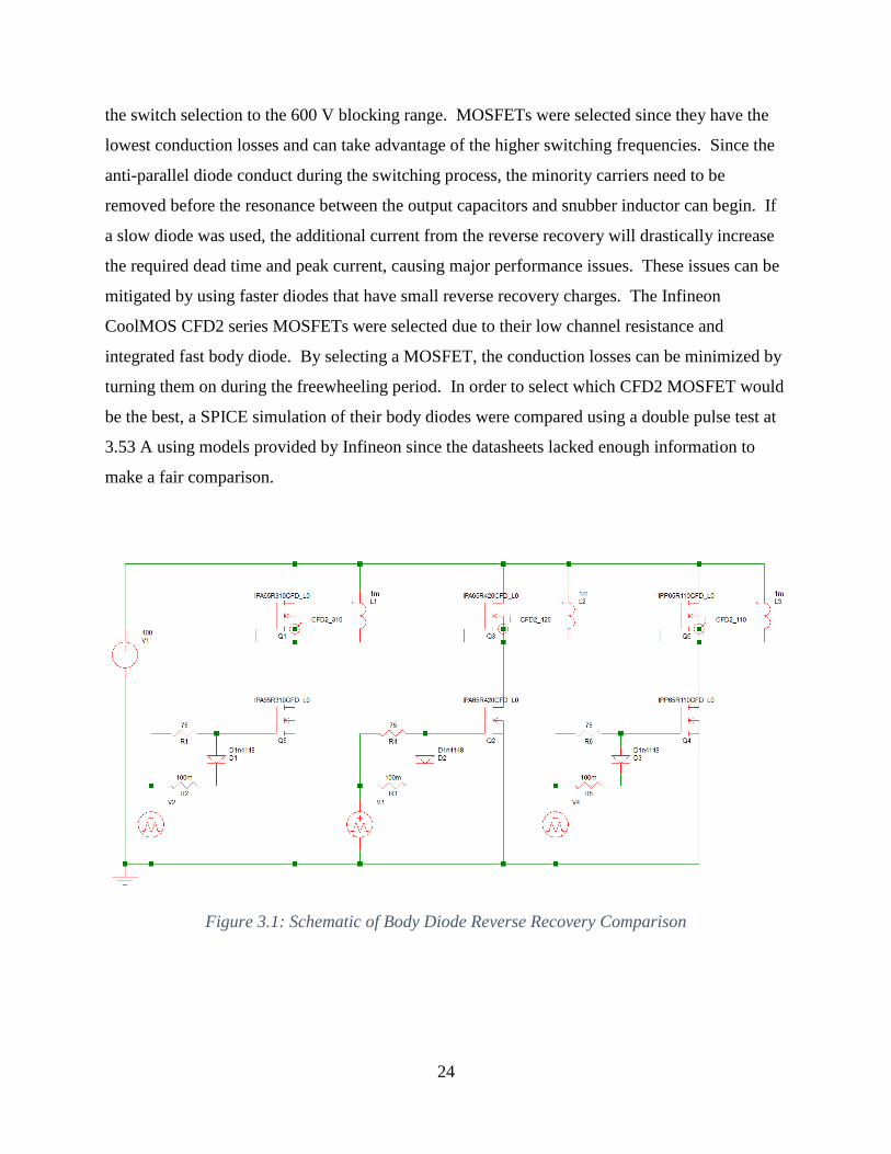
3.1 Power Stage Switch Selection ........................................................................................ 23
3.2 Auxiliary Resonant Snubber Capacitor .......................................................................... 26
3.3 Auxiliary Resonant Snubber Inductor for Adaptive Case (a) ........................................ 27
3.4 Adaptive Auxiliary Resonant Snubber Control Timing for Adaptive Case (a) ............. 30
3.5 Auxiliary Resonant Snubber Inductor for Adaptive Case (b) ........................................ 32
3.6 Auxiliary Resonant Snubber Switch .............................................................................. 33
3.7 Switching Frequency ...................................................................................................... 35
3.8 DC Bus Voltage ............................................................................................................. 35
3.9 Output Filter ................................................................................................................... 36
3.10 Design Summary ............................................................................................................ 37
3.11 Power Stage Hardware Test Setup ................................................................................. 37
3.12 Auxiliary Voltage Overshoot Issue ................................................................................ 39
3.13 Power Stage Experimental Results ................................................................................ 43

vi
3.14 Efficiency Measurement ................................................................................................ 49
3.15 Thermal Measurement Loss Analysis ............................................................................ 51
4 Control ................................................................................................................................... 56
4.1 Standalone Mode Control............................................................................................... 56
4.1.1 Standalone Mode Plant Model ................................................................................ 56
4.1.2 Design of Standalone Controller ............................................................................. 57
4.1.3 Simulation of Standalone Controller ...................................................................... 60
4.1.4 Experimental Results of Standalone Controller ...................................................... 62
4.2 Grid Tie Control ............................................................................................................. 65
4.2.1 Phase Lock Loop..................................................................................................... 66
4.2.2 Grid Tie Plant Model .............................................................................................. 67
4.2.3 Control Block Diagram ........................................................................................... 69
4.2.4 Current Loop Control Compensator Design ........................................................... 70
4.2.5 Feed Forward Compensator Design ........................................................................ 73
4.2.6 Simulation of Grid Tie Controller........................................................................... 73
4.2.7 Experimental Results of Grid Tie Controller .......................................................... 74
5 Conclusion ............................................................................................................................. 78
5.1 Future Work ................................................................................................................... 79
References ..................................................................................................................................... 80

vii
TABLE OF FIGURES
Figure 1.1: Traditional Central String Inverter ............................................................................... 2
Figure 1.2: Microinverter ................................................................................................................ 3
Figure 1.3: Microconverter with Parallel Connection .................................................................... 4
Figure 1.4: Dual Buck Inverter Schematic ..................................................................................... 6
Figure 1.5: H5 Inverter Schematic .................................................................................................. 7
Figure 1.6: HERIC Inverter Schematic ........................................................................................... 8
Figure 1.7: Auxiliary Resonant Snubber with Capacitor Reset Schematic .................................... 9
Figure 1.8: Auxiliary Resonant Snubber with Coupled Magnetic Reset Schematic .................... 10
Figure 1.9: Auxiliary Resonant Snubber with No External Reset ................................................ 11
Figure 2.1: Resonant Snubber Inverter Schematic ....................................................................... 13
Figure 2.2: Two Auxiliary Resonant Snubber Control Methods .................................................. 14
Figure 2.3: Adaptive Control Method of Auxiliary Resonant Snubber with Case (a) ................. 15
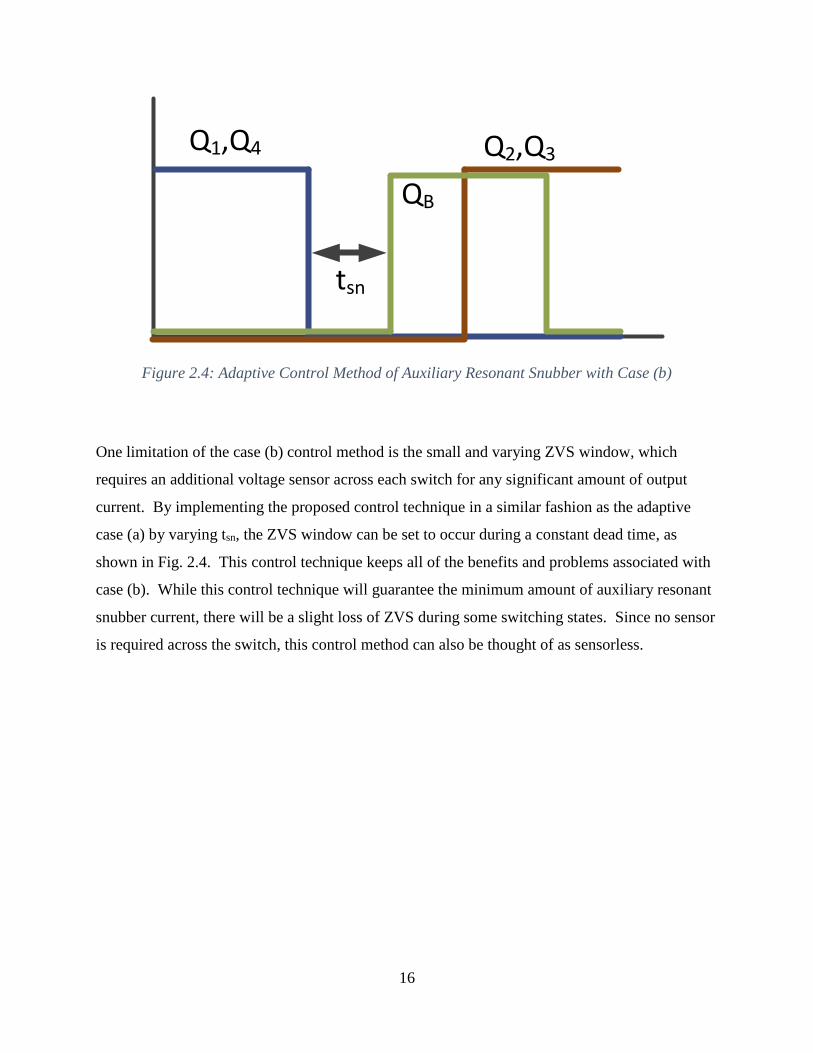
Figure 2.4: Adaptive Control Method of Auxiliary Resonant Snubber with Case (b) ................. 16
Figure 2.5: Schematic and Timing Diagram with Positive Load Current .................................... 17
Figure 2.6: Schematic with Negative Load Current ..................................................................... 19
Figure 2.7: Timing Diagram with Negative Load Current and Case (a) Control ......................... 20
Figure 3.1: Schematic of Body Diode Reverse Recovery Comparison ........................................ 24
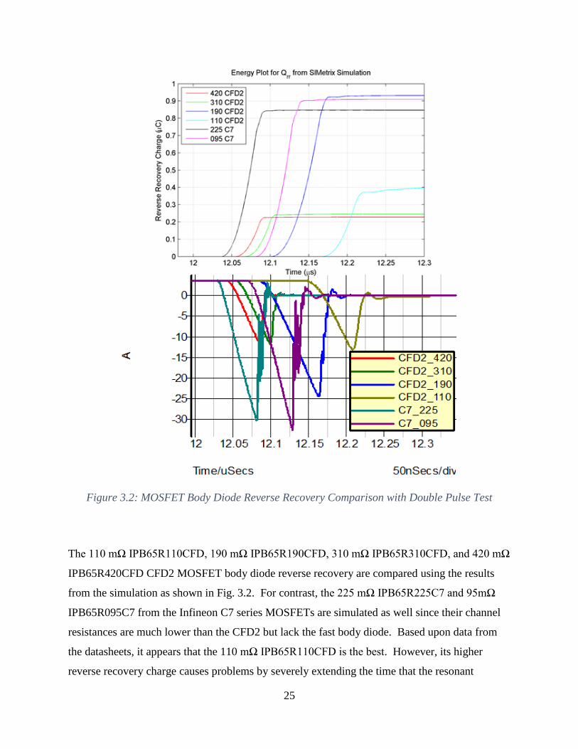
Figure 3.2: MOSFET Body Diode Reverse Recovery Comparison with Double Pulse Test....... 25
Figure 3.3: Resonant Snubber Current caused by Lr .................................................................... 27
Figure 3.4: PSIM Simulation of Switching Action when Iout is 0.5 A .......................................... 28
Figure 3.5: PSIM Simulation of Switching Action for Adaptive Case (a) Control when Iout is 3.5
A .................................................................................................................................................... 30
Figure 3.6: PSIM Simulation of Switching Action for Adaptive Case (b) Control when Iout is 3.5
A .................................................................................................................................................... 32
Figure 3.7: Cascade Configuration of TPH3006 .......................................................................... 34
Figure 3.8: Experimental Test Setup ............................................................................................ 38
Figure 3.9: Experimental Test PCB .............................................................................................. 38
Figure 3.10: Waveform of Switching Action with Voltage Overshoot Issue ............................... 40
Figure 3.11: Waveform of Switching Action with Separate Resonant Snubber Legs .................. 41

viii
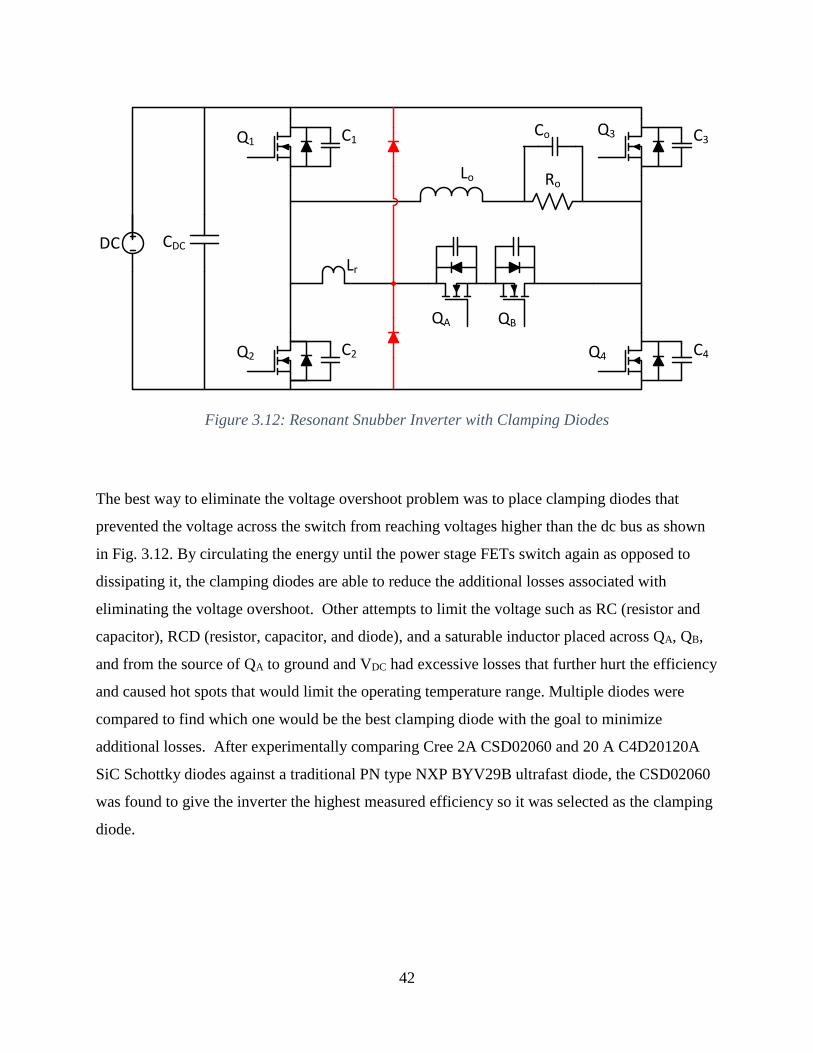
Figure 3.12: Resonant Snubber Inverter with Clamping Diodes .................................................. 42
Figure 3.13: Waveform of Switching Action during High Line Current ..................................... 43
Figure 3.14: Waveform of Switching Action during Low Line Current ...................................... 44
Figure 3.15: Waveform of Output with Adaptive Case (a) Control and 600 W (100%) Output
Power ............................................................................................................................................ 45
Figure 3.16: Waveform of Output with Adaptive Case (a) Control and60 W (10%) Output Power
....................................................................................................................................................... 46
Figure 3.17: Waveform of Output with Simple Case (a) Control and 600 W (100%) Output
Power ............................................................................................................................................ 47
Figure 3.18: Waveform of Output with Adaptive Case (b) Control and 600 W (100%) Output
Power ............................................................................................................................................ 48
Figure 3.19: Measured Efficiency over CEC Operating Range ................................................... 49
Figure 3.20: Photo of Thermal Measurement Point of Auxiliary Resonant Snubber ................... 52
Figure 3.21: Thermal Measurement of Auxiliary Resonant Snubber at 120 W and 600 W Output
....................................................................................................................................................... 52
Figure 3.22: Photo of Thermal Measurement Point of Output Inductor....................................... 53
Figure 3.23: Thermal Measurement of Output Inductor at 120 W Output and 600 W Output .... 53
Figure 3.24: Photo of Thermal Measurement Point of Power Stage Switches ............................. 54
Figure 3.25: Thermal Measurement of Power Stage Switches at 120 W Output and 600 W
Output ........................................................................................................................................... 54
Figure 4.1: Bode Plot of Control to Output Voltage ..................................................................... 57
Figure 4.2: Block Diagram of Standalone Controller ................................................................... 57
Figure 4.3: Bode Plot of Loop Gain and Controller ..................................................................... 58
Figure 4.4: Comparison between Continuous and Discrete Time Domain of Standalone
Controller ...................................................................................................................................... 59
Figure 4.5: PSIM Simulation of Output Waveforms .................................................................... 60
Figure 4.6: PSIM Simulation of 100% to 10% Load Step ............................................................ 61
Figure 4.7: Waveform of Output with Standalone Control .......................................................... 62
Figure 4.8: Waveform of Output During 20% to 100% Load Step with Standalone Controller .. 63
Figure 4.9: Close Up Waveform of Output with Standalone Control .......................................... 64
Figure 4.10: Schematic of Grid Tie Resonant Snubber Inverter .................................................. 65

ix
Figure 4.11: Block Diagram of Phase Locked Loop .................................................................... 66
Figure 4.12: Loop Gain of Phase Locked Loop ............................................................................ 66
Figure 4.13: PSIM Simulation of Phase Locked Loop (Red: Input, Blue: Output)...................... 67
Figure 4.14: Bode Plot of Control to Inductor Current ................................................................. 68
Figure 4.15: Grid Tie Control Block Diagram.............................................................................. 69
Figure 4.16: Comparison between Continuous and Discrete Time Domain of Grid Tie Controller
....................................................................................................................................................... 71
Figure 4.17: Current Loop Gain of Grid Tie Control ................................................................... 72
Figure 4.18: PSIM Simulation of Grid Tie Control under Full Load ........................................... 73
Figure 4.19: Waveform of Output with Grid Tie Control under Full Load .................................. 76

x
TABLE OF TABLES
Table 3.1: Specification Parameters ............................................................................................. 23
Table 3.2: Auxiliary Resonant Snubber Adaptive Timing for Adaptive Case (a) ........................ 31
Table 3.3: Auxiliary Resonant Snubber Adaptive Timing for Adaptive Case (b)........................ 33
Table 3.4: Parameter Values from Design .................................................................................... 37
Table 3.5: Ideal and Measured Output Power Levels ................................................................... 50
Table 3.6: Measured Efficiency of Various Control Methods ...................................................... 50
Table 4.1: Standalone Closed Loop Operating Parameters .......................................................... 59
Table 4.2: Standalone Controller Steady State Simulation Results .............................................. 61
Table 4.3: Standalone Controller Dynamic Simulation Results ................................................... 61
Table 4.4: Measured Steady State Operating Parameters ............................................................. 62
Table 4.5: Grid Tie Current Closed Loop Operating Parameters ................................................. 72
Table 4.6: Maximum Harmonic Current Distortion in Percent of Current from IEEE Std. 1547 74
Table 4.7: Harmonic Content of Grid Tie Output Current under Full Load ................................. 77

1
1 INTRODUCTION
As renewable energy sources become cheaper and more prevalent, there is an increasing desire
for inexpensive and efficient means of converting this power to work with the existing electrical
utility grid. One common source is photovoltaics. With recent decreases in cost and government
programs such as Solarize Mass [1] and Go Solar California [2] to help further subsidize the
price, this renewable energy source is becoming affordable and practical for homeowners to
install. These incentives have help solar to be the fastest growing alternative energy source, with
growth expectations from $11B in 2005 to $51B in 2015 [3]. To take full advantage of this
renewable energy, the dc voltage from the solar panel has to be converted to ac voltage in a
highly efficient and low cost manner. In order to draw the most power out of the panel possible,
a maximum power point tracking (MPPT) algorithm needs to be implemented, which is usually
done with a dc/dc converter [3]. To work with the existing utility power grid or household
appliances that run off of ac power, a second inverter stage is needed to convert the dc to ac.
There are multiple ways that this conversion from panel voltage to utility grid can be
implemented, from the traditional central string inverter to the microinverter to the
microconverter with a centralized dc/ac inverter. Previously, the most popular architecture is the
traditional central string inverter, but a large amount of generated energy is wasted due to limited
power optimization. Microinverters have been introduced to overcome this issue, but, due to
high additional part count, the cost is prohibitive for higher power level applications. The
microconverter with centralized inverter has the potential to overcome these issues, but they have
not been commercially yet developed due to the additional complexity and cost.

2
1.1 TRADITIONAL CENTRAL STRING INVERTER
Traditionally, a single dc/dc and dc/ac converter are used to convert the dc energy from the solar
panel to ac power that can be connected to the utility grid [4]. There are many commercial
products currently available from various manufactures, such as Power-One Aurora Uno Series
and SMA Sunny Boy Series[5, 6]. This is schematically shown in Fig. 1.1.
dc/dcMPPT
Controldc/ac AC Grid
Figure 1.1: Traditional Central String Inverter
Due to the minimal additional components, this architecture has the benefits of low cost and
simple installation. By connecting all of the panels in series, the total power of the system is
limited by each individual panel. Thus, one single shaded panel is able to cause large reductions
in total output power. Since partial shading on the solar panels is common, the output power of
the system is often times significantly less than the available power generated.

3
1.2 MICROINVERTER
The most efficient way to optimize the power delivery for a photovoltaic installation is to have a
dedicated maximum power point tracking converter that is attached to each individual solar
panel. Currently this is achieved with microinverters, which are small inverter modules that
perform both the MPPT and dc/ac inversion for a single solar panel. There are two ways that the
microinverter can be implemented, a two-stage solution that is similar to the traditional central
string inverter (Fig. 1.2 a), or a one-stage solution that performs both the MPPT and dc/ac
inversion at once (Fig. 1.2 b).
dc/dcMPPT
Controldc/ac AC Grid
dc/acMPPT
ControlAC Grid
Case (a) Two Stage
Case (b) One Stage
Figure 1.2: Microinverter
By reducing the total components with the elimination of a stage the one stage solution generally
achieves higher efficiency. This requires a large electrolytic capacitor bank since the double line
frequency ripple from the ac grid can decrease the available power from the solar panel that is
4
delivered to the load. The large capacitor reduces lifetime and reliability since these inverters
generally tend to operate outdoors where there are large temperature variations. Many
commercial products are currently available, such as Power-One Aurora Micro and Solarbridge
Pantheon II for the two stage solution and Enphase for the one stage solution [7-9]. While both
implementations allow for high efficiency and power optimization for each panel, the cost is
drastically increased for large solar panel installations due to the dedicated dc/ac inverter for
each panel.
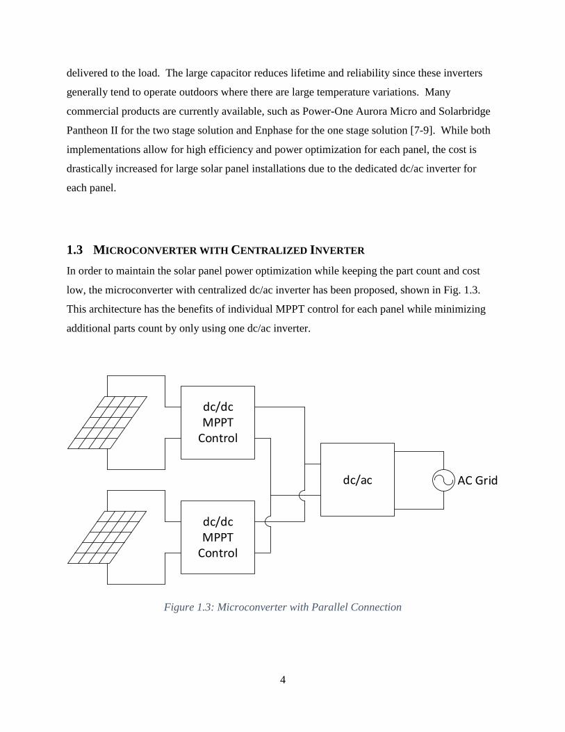
1.3 MICROCONVERTER WITH CENTRALIZED INVERTER
In order to maintain the solar panel power optimization while keeping the part count and cost
low, the microconverter with centralized dc/ac inverter has been proposed, shown in Fig. 1.3.
This architecture has the benefits of individual MPPT control for each panel while minimizing
additional parts count by only using one dc/ac inverter.
dc/dcMPPT
Control
dc/dcMPPT
Control
dc/ac AC Grid
Figure 1.3: Microconverter with Parallel Connection

5
The only commercial product currently available that utilizes this implementation is Texas
Instruments (formally National Semiconductor) SolarMagic. Unlike Figure 3, the dc/dc
converters in the TI SolarMagic are connected in series to the dc/ac inverter as opposed to
parallel [10]. The problem with series connected dc/dc converters is that many are needed in
order to reach voltages high enough for grid connection. This problem is solved with parallel
connections, but this requires less efficient high voltage gain dc/dc converters [11, 12].
1.4 INVERTER REQUIREMENTS
All of these implementations require inverters that operate at high efficiency while minimizing
cost and conform to various standards in order to be attached to the utility grid. Traditional full
bridge inverters, while the most simple to implement, have many issues such as low efficiency,
large size, high cost, and generation of electronic noise. In order to solve these problems and
take full advantage of improved architecture designs like the microinverter and microconverter
with central dc/ac inverter, improvements need to be made on the inverter stage.

6
1.5 HIGH EFFICIENCY HARD SWITCHING INVERTERS
One popular way to limit the losses of the inverter is to minimize the switching losses by
reducing the number of high frequency pulse with modulated (PWM) switches. Since the
switching losses are a major source of loss the efficiency of the converter is improved by
minimizing the number of switches operating at high frequency.
DC AC
Figure 1.4: Dual Buck Inverter Schematic
The dual buck inverter shown in Fig. 1.4 achieves this by having two separate buck converters,
with one generating the positive and the other generating the negative line cycle. This allows
only two high frequency PWM switches to run at any given time, which allows the inverter to
achieve a peak efficiency of 99% [13]. By utilizing two separate converters, this topology
suffers many drawbacks such as poor magnetic utilization, zero crossing distortion, and large
common mode noise from the unipolar style switching. Attempts to fix these problems reduce
the zero crossing and magnetic utilization issues, but these drawbacks still cause major problems
[14].

7
DC AC
Figure 1.5: H5 Inverter Schematic
A topology that was developed by SMA to eliminate the common mode noise while achieving
high efficiency by minimizing high frequency switches is the H5 inverter shown in Fig. 1.5 [15].
By adding an additional switch before a unipolar switching full bridge converter, the common
mode noise issue is eliminated. But, this topology requires higher loss isolated gate bipolar
transistors (IGBTs) with fast body diodes for the low frequency switches, and along with an
extra semiconductor device the number of parts and cost are increased. This causes the
efficiency to drop slightly with a reported peak of 98.7% for a 6 kW system under ideal
operating conditions [6]. Attempts to improve the drawbacks of the H5 with topographies such
as the H6 improve the efficiency by eliminating the IGBTs with more efficient MOSFETs, but
the extra switch needed to eliminate the common mode noise further increases the high costs and
limits the efficiency [16]. In order to maintain the high efficiency of the dual buck inverter while
eliminating the common mode noise, new topologies have been derived from these circuits, but,
like the dual buck, they suffer from poor magnetic utilization and high part count, which increase
the size and cost [17].
8
DC
Lo Ro
QBQA
Q1
Q2
Q3
Q4
CDC
Figure 1.6: HERIC Inverter Schematic
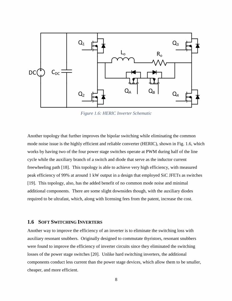
Another topology that further improves the bipolar switching while eliminating the common
mode noise issue is the highly efficient and reliable converter (HERIC), shown in Fig. 1.6, which
works by having two of the four power stage switches operate at PWM during half of the line
cycle while the auxiliary branch of a switch and diode that serve as the inductor current
freewheeling path [18]. This topology is able to achieve very high efficiency, with measured
peak efficiency of 99% at around 1 kW output in a design that employed SiC JFETs as switches
[19]. This topology, also, has the added benefit of no common mode noise and minimal
additional components. There are some slight downsides though, with the auxiliary diodes
required to be ultrafast, which, along with licensing fees from the patent, increase the cost.
1.6 SOFT SWITCHING INVERTERS
Another way to improve the efficiency of an inverter is to eliminate the switching loss with
auxiliary resonant snubbers. Originally designed to commutate thyristors, resonant snubbers
were found to improve the efficiency of inverter circuits since they eliminated the switching
losses of the power stage switches [20]. Unlike hard switching inverters, the additional
components conduct less current than the power stage devices, which allow them to be smaller,
cheaper, and more efficient.
9
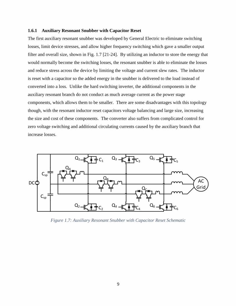
1.6.1 Auxiliary Resonant Snubber with Capacitor Reset
The first auxiliary resonant snubber was developed by General Electric to eliminate switching
losses, limit device stresses, and allow higher frequency switching which gave a smaller output
filter and overall size, shown in Fig. 1.7 [21-24]. By utilizing an inductor to store the energy that
would normally become the switching losses, the resonant snubber is able to eliminate the losses
and reduce stress across the device by limiting the voltage and current slew rates. The inductor
is reset with a capacitor so the added energy in the snubber is delivered to the load instead of
converted into a loss. Unlike the hard switching inverter, the additional components in the
auxiliary resonant branch do not conduct as much average current as the power stage
components, which allows them to be smaller. There are some disadvantages with this topology
though, with the resonant inductor reset capacitors voltage balancing and large size, increasing
the size and cost of these components. The converter also suffers from complicated control for
zero voltage switching and additional circulating currents caused by the auxiliary branch that
increase losses.
DC
Csp
Csp
Q1 C1
Q2 C2
Q3 C3
Q4 C4
Q5 C5
Q6 C6
QA
QB
QC
ACGrid
Figure 1.7: Auxiliary Resonant Snubber with Capacitor Reset Schematic
10
1.6.2 Auxiliary Resonant Snubber with Coupled Magnetic Reset
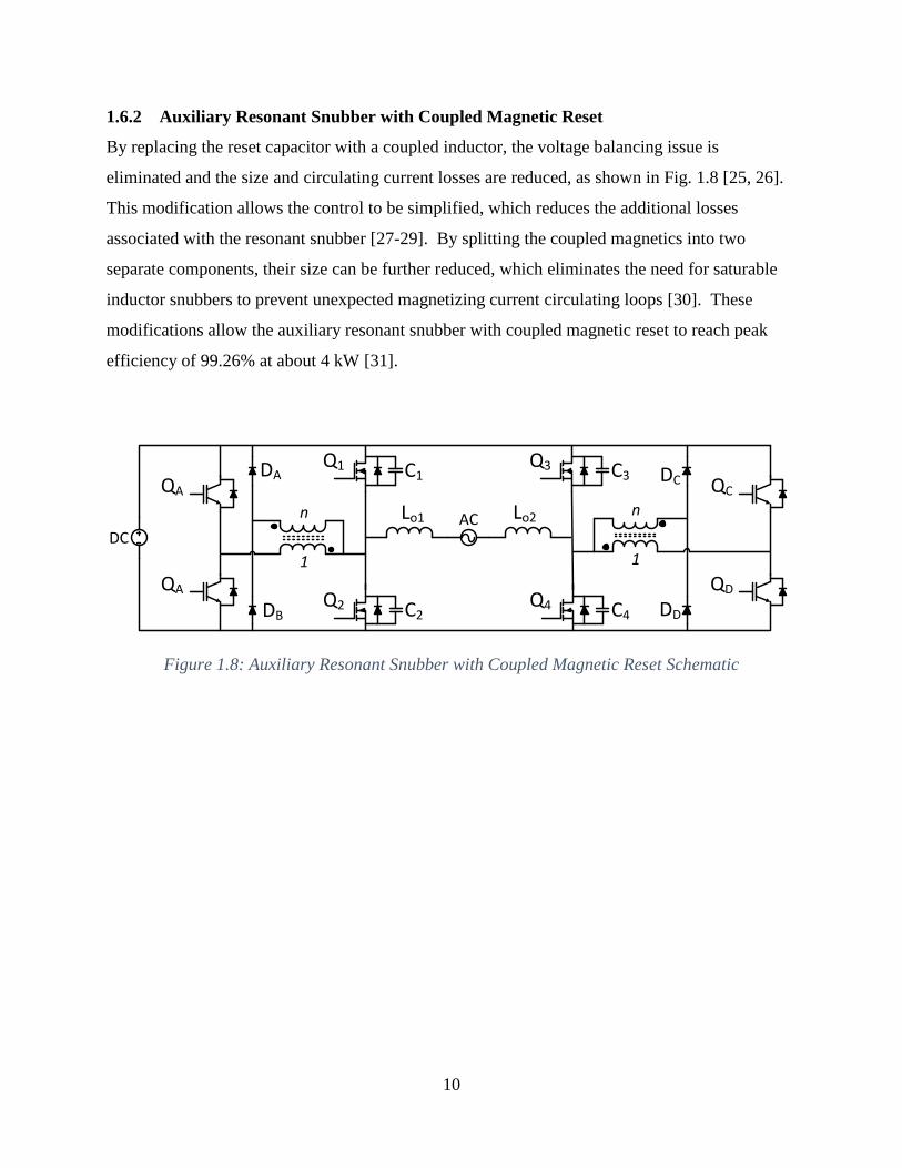
By replacing the reset capacitor with a coupled inductor, the voltage balancing issue is
eliminated and the size and circulating current losses are reduced, as shown in Fig. 1.8 [25, 26].
This modification allows the control to be simplified, which reduces the additional losses
associated with the resonant snubber [27-29]. By splitting the coupled magnetics into two
separate components, their size can be further reduced, which eliminates the need for saturable
inductor snubbers to prevent unexpected magnetizing current circulating loops [30]. These
modifications allow the auxiliary resonant snubber with coupled magnetic reset to reach peak
efficiency of 99.26% at about 4 kW [31].
DC
C1Q1
C2Q2
1
n
QA
QA
AC
C3Q3
C4Q4
1
n
QC
QD
DD
DCDA
DB
Lo1 Lo2
Figure 1.8: Auxiliary Resonant Snubber with Coupled Magnetic Reset Schematic
11
1.6.3 Auxiliary Resonant Snubber with No External Reset
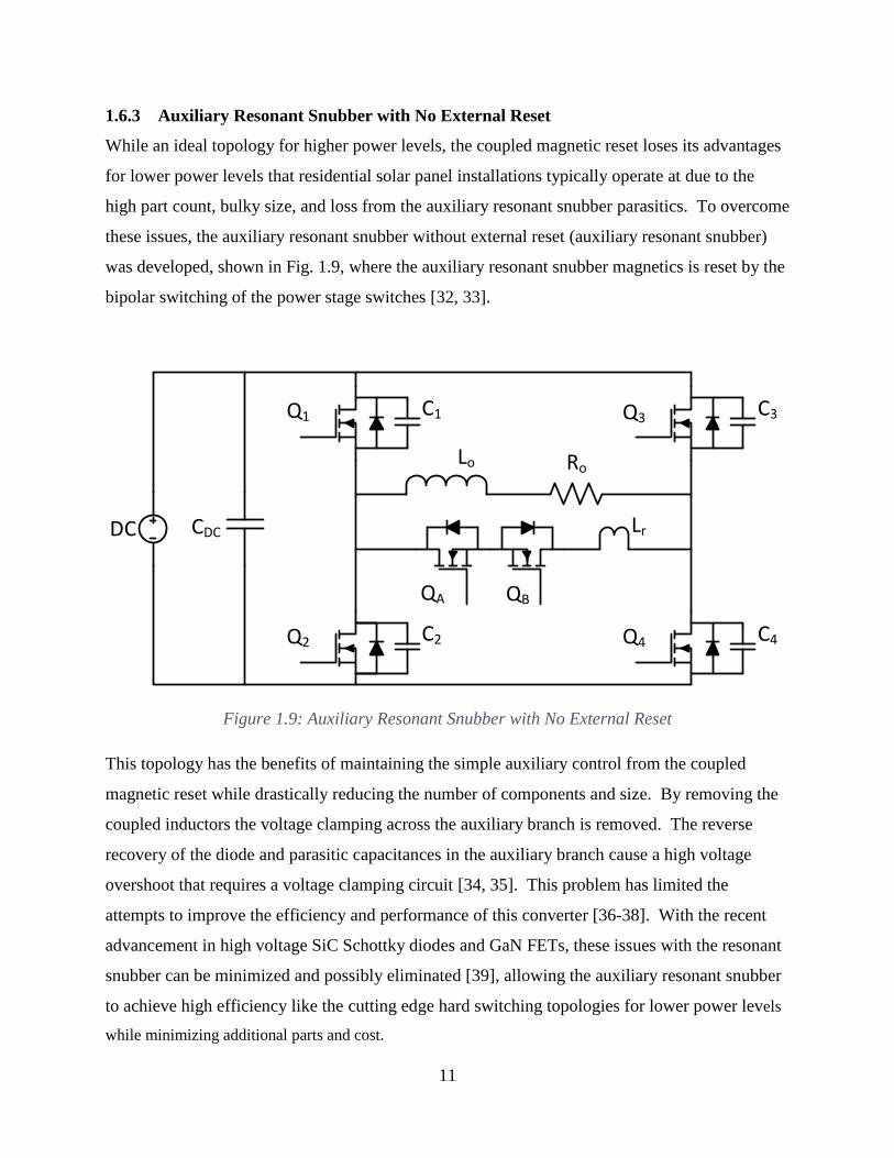
While an ideal topology for higher power levels, the coupled magnetic reset loses its advantages
for lower power levels that residential solar panel installations typically operate at due to the
high part count, bulky size, and loss from the auxiliary resonant snubber parasitics. To overcome
these issues, the auxiliary resonant snubber without external reset (auxiliary resonant snubber)
was developed, shown in Fig. 1.9, where the auxiliary resonant snubber magnetics is reset by the
bipolar switching of the power stage switches [32, 33].
DC
Lo Ro
QBQA
Q1
Q2
Q3
Q4
CDC
C1
Lr
C3
C4C2
Figure 1.9: Auxiliary Resonant Snubber with No External Reset
This topology has the benefits of maintaining the simple auxiliary control from the coupled
magnetic reset while drastically reducing the number of components and size. By removing the
coupled inductors the voltage clamping across the auxiliary branch is removed. The reverse
recovery of the diode and parasitic capacitances in the auxiliary branch cause a high voltage
overshoot that requires a voltage clamping circuit [34, 35]. This problem has limited the
attempts to improve the efficiency and performance of this converter [36-38]. With the recent
advancement in high voltage SiC Schottky diodes and GaN FETs, these issues with the resonant
snubber can be minimized and possibly eliminated [39], allowing the auxiliary resonant snubber
to achieve high efficiency like the cutting edge hard switching topologies for lower power levels
while minimizing additional parts and cost.

12
1.7 GOAL AND SCOPE OF THESIS
The goal of this thesis is to take advantage of new semiconductor materials and novel control
techniques of the auxiliary resonant snubber to allow the inverter to achieve high efficiency
while minimizing additional parts and maintaining simple control. The basic operation of the
resonant snubber is presented in Section 2 along with a demonstration on how the inverter
achieves zero voltage switching (ZVS) while proposing techniques to minimize additional
circulating currents without any additional sensors or parts. In Section 3, a detailed design of all
of the components and parameters of a 600 W prototype and experimental results to verify the
inverter performance are described. A design and experimental test of standalone and grid tie
control to demonstrate that the auxiliary resonant snubber does not add any additional
complexity to closed loop control is discussed in Section 4. Section 5 is a summary of the results
of the design and experimental results and a discussion on potential future work to further
improve the resonant snubber inverter and overcome limitations of current inverters.
13
2 RESONANT SNUBBER INVERTER BASIC OPERATION
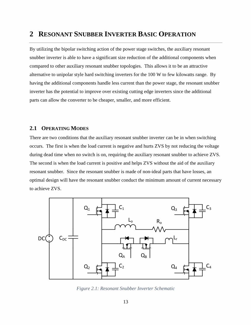
By utilizing the bipolar switching action of the power stage switches, the auxiliary resonant
snubber inverter is able to have a significant size reduction of the additional components when
compared to other auxiliary resonant snubber topologies. This allows it to be an attractive
alternative to unipolar style hard switching inverters for the 100 W to few kilowatts range. By
having the additional components handle less current than the power stage, the resonant snubber
inverter has the potential to improve over existing cutting edge inverters since the additional
parts can allow the converter to be cheaper, smaller, and more efficient.
2.1 OPERATING MODES
There are two conditions that the auxiliary resonant snubber inverter can be in when switching
occurs. The first is when the load current is negative and hurts ZVS by not reducing the voltage
during dead time when no switch is on, requiring the auxiliary resonant snubber to achieve ZVS.
The second is when the load current is positive and helps ZVS without the aid of the auxiliary
resonant snubber. Since the resonant snubber is made of non-ideal parts that have losses, an
optimal design will have the resonant snubber conduct the minimum amount of current necessary
to achieve ZVS.
Figure 2.1: Resonant Snubber Inverter Schematic
DC
Lo Ro
QBQA
Q1
Q2
Q3
Q4
CDC
C1
Lr
C3
C4C2
14
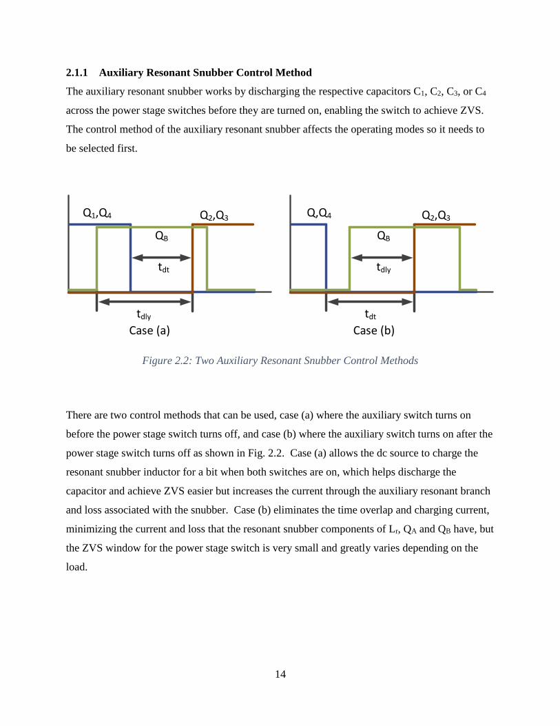
2.1.1 Auxiliary Resonant Snubber Control Method
The auxiliary resonant snubber works by discharging the respective capacitors C1, C2, C3, or C4
across the power stage switches before they are turned on, enabling the switch to achieve ZVS.
The control method of the auxiliary resonant snubber affects the operating modes so it needs to
be selected first.
Q1,Q4 Q2,Q3
QB
tdly
tdt
Q,Q4 Q2,Q3
QB
tdt
tdly
Case (a) Case (b)
Figure 2.2: Two Auxiliary Resonant Snubber Control Methods
There are two control methods that can be used, case (a) where the auxiliary switch turns on
before the power stage switch turns off, and case (b) where the auxiliary switch turns on after the
power stage switch turns off as shown in Fig. 2.2. Case (a) allows the dc source to charge the
resonant snubber inductor for a bit when both switches are on, which helps discharge the
capacitor and achieve ZVS easier but increases the current through the auxiliary resonant branch
and loss associated with the snubber. Case (b) eliminates the time overlap and charging current,
minimizing the current and loss that the resonant snubber components of Lr, QA and QB have, but
the ZVS window for the power stage switch is very small and greatly varies depending on the
load.

15
Q1,Q4 Q2,Q3
QB
tsn
Figure 2.3: Adaptive Control Method of Auxiliary Resonant Snubber with Case (a)
In order to maximize the benefits of both cases, an adaptive control method for the auxiliary
resonant snubber based off of case (a) is proposed, as shown in Fig. 2.3. Instead of running a
fixed time control, the time between the auxiliary switch turn on and power stage turn off (tsn) is
varied as a function of the load current. By adjusting this time, the inductance of the resonant
snubber can be selected to be ideal at low output current levels, which will limit the frequency
and peak current of the resonant snubber and in turn decrease additional losses. As the load
increases and the ZVS window changes, tsn and the charging current can be increased to allow a
fixed dead time to still achieve ZVS. Since the auxiliary resonant snubber operates like case (a)
during negative high current line conditions, ZVS is able to be easily achieved. As the load
current becomes large enough in the positive direction where it helps ZVS, the auxiliary resonant
snubber is disabled, allowing the circuit to naturally achieve ZVS without any additional losses.
This control is able to be implemented with only one sensor for the output inductor current.
Since this sensor is already required for control and protection purposes, the adaptive control
method can be thought of as sensorless.
16
Q1,Q4 Q2,Q3
QB
tsn
Figure 2.4: Adaptive Control Method of Auxiliary Resonant Snubber with Case (b)
One limitation of the case (b) control method is the small and varying ZVS window, which
requires an additional voltage sensor across each switch for any significant amount of output
current. By implementing the proposed control technique in a similar fashion as the adaptive
case (a) by varying tsn, the ZVS window can be set to occur during a constant dead time, as
shown in Fig. 2.4. This control technique keeps all of the benefits and problems associated with
case (b). While this control technique will guarantee the minimum amount of auxiliary resonant
snubber current, there will be a slight loss of ZVS during some switching states. Since no sensor
is required across the switch, this control method can also be thought of as sensorless.
17
2.1.2 Operating Mode with Positive Load Current
When load current is large enough and the dead time between the power stage switches is long
enough, the auxiliary resonant snubber is not needed since the load current can allow the
switches to achieve ZVS.
DC
Lo Ro
QBQA
Q1
Q2
Q3
Q4
C1
Lr
C3
C4C2
Iload
DC
Lo Ro
QBQA
Q1
Q2
Q3
Q4
C1
Lr
C3
C4C2
Iload
DC
Lo Ro
QBQA
Q1
Q2
Q3
Q4
C1
Lr
C3
C4C2
Iload
t0 – t1
t1 – t2
t2 – t3
Q1,Q4
tdt
Q2,Q3
VDS Q2,Q3 VDS Q1,Q4
t0 t1 t2 t3
I
I
I
I
DC
Lo Ro
QBQA
Q1
Q2
Q3
Q4
C1
Lr
C3
C4C2
Iload
t3 – t4
t4
Figure 2.5: Schematic and Timing Diagram with Positive Load Current

18
This transition occurs when the switches transition to have the dc bus voltage vary from positive
to negative across the load. As Figure 12 shows:
a) Between to – t1: The load current flows through Q1 and Q4.
b) Between t1 – t2: At t1, Q1 and Q4 turn off. As time increases, the load current causes the
capacitors C1 and C4 to charge, causing the voltage across Q1 and Q4to increase to VDC
and the capacitors C2 and C3 to discharge, which then cause the voltage across Q2 and Q3
to drop to zero.
c) Between t2 – t3: At t2, the voltage across Q2 and Q3 reach zero, causing their anti-parallel
diodes to conduct. This begins the ZVS window for Q2 and Q3.
d) Between t3 – t4: At t3, the switches Q2 and Q3 are turned on if they are MOSFETs to
reduce the conduction losses of the switches, completing the switching action. If IGBTs
are used then the antiparallel diode will conduct since it is not a bidirectional device like
a MOSFET.
By not using the auxiliary snubber to achieve ZVS between t1 and t2, the discharge time of the
output capacitors is extended slightly, but the additional losses that occur from the resonant
snubber conducting are eliminated. When the magnitude of the load current is large enough, this
is not a problem. However, as the current becomes very small, this time increases, requiring the
auxiliary resonant snubber to be enabled to achieve ZVS even though the line current is positive.
19
2.1.3 Operating Mode with Negative Load Current
When the load current is in the opposite direction, the auxiliary resonant snubber is needed to
achieve ZVS. The basic operating principle is that the net current at the switching nodes needs
to change direction for ZVS to be achieved, which the resonant snubber achieves.
DC
Lo Ro
QBQA
Q1
Q2
Q3
Q4
C1
Lr
C3
C4C2
Iload
t0 – t1
DC
Lo Ro
QBQA
Q1
Q2
Q3
Q4
C1
Lr
C3
C4C2
Iload
t1 – t2
Isnubber
DC
Lo Ro
QBQA
Q1
Q2
Q3
Q4
C1
Lr
C3
C4C2
Iload
t2 – t3
I
I
I
I
Isnubber
DC
Lo Ro
QBQA
Q1
Q2
Q3
Q4
C1
Lr
C3
C4C2
Iload
t3 – t4
Isnubber
DC
Lo Ro
QBQA
Q1
Q2
Q3
Q4
C1
Lr
C3
C4C2
Iload
t4 – t5
Isnubber
DC
Lo Ro
QBQA
Q1
Q2
Q3
Q4
C1
Lr
C3
C4C2
Iload
t5 – t6
Figure 2.6: Schematic with Negative Load Current

20
Q2,Q3 Q1,Q4
VDS Q1,Q4 VDS Q2,Q3
t0 t1
QB
t2 t3 t4 t5 t6
Iload
Isnubber
Figure 2.7: Timing Diagram with Negative Load Current and Case (a) Control
21
This transition occurs when the switches transition to have the dc bus voltage vary from negative
to positive across the load. As Figure 13 and Figure 14 show:
a) Between to – t1: The load current flows through Q2 and Q3.
b) Between t1 – t2: The switch QB is turned on at t1, which allows Lr to begin conducting
current as the anti-parallel diode of QA turn on. Before Q2 and Q3 are turned off, Lr is
charged by the dc bus, which allows ZVS to be achieved more easily. Q2 and Q3 are
turned off during this time, but the anti-parallel diodes of Q2 and Q3 conduct since the
load current is still larger than the snubber current.
c) Between t2 – t3: At t2, the snubber current becomes larger than the load current. This
causes the net direction of the current at switches to change, which causes the voltage
across Q2 and Q3 to rise to VDC and the voltage across Q1 and Q4 to drop to zero.
e) Between t3 – t4: At t3, the voltage across Q1 and Q4 reach zero and their anti-parallel
diodes start to conduct. This begins the ZVS window.
d) Between t4 – t5: At t4, Q1 and Q4 turn on with ZVS and the dc voltage across the load and
auxiliary resonant snubber changes direction. The current through Lr decreases to zero
and the anti-parallel diode of QA prevents any more current to go through the auxiliary
branch.
e) Between t5 – t6: At t5, QB is turned off under zero current condition, completing the
switching action.
By placing external capacitors across each power stage switch, the resonant time can be more
predictable and consistent between switches due to the highly nonlinear and variation of the
internal output capacitance of each switch. If the capacitance is large enough, it will absorb the
turn off energy, which means that all of the switching losses can be minimized along with the
turn on loss eliminated from the auxiliary resonant snubber to the point where they are
negligible. This increase in capacitance also requires larger snubber current to achieve ZVS,
which increases the additional losses of the auxiliary resonant snubber, making it important to
prevent excessive external capacitances. By utilizing the diode to turn off the auxiliary resonant
snubber, QA and QB are naturally turned off, achieving zero current switching. This allows QA
and QB to be turned off without any additional losses without precise timing, simplifying the
control and minimizing additional loss. The case (b) auxiliary resonant snubber control method

22
works in a similar fashion with the exception that the primary switches are turned off before the
auxiliary switch turns on, eliminating the time where Lr is charged by the dc bus.
2.2 DESIGN LIMITATIONS
As ZVS is achieved by utilizing the auxiliary resonant snubber, there are some additional
limitations that impact the design of the inverter. In order to prevent the auxiliary resonant
snubber action from interfering with other switching actions, the effective dead time is increased
which requires higher dc bus voltages to achieve a desired output voltage. The resonant snubber
also has losses associated with the switch, diode, and inductor so excessive auxiliary resonant
currents are undesired since they decrease the efficiency of the converter. These losses increase
with higher switching frequencies. Even though the switching losses are eliminated, the
frequency cannot be drastically increased.

23
3 PARAMETER DESIGN
To verify the improvements that newer generations of semiconductor devices and proposed
auxiliary resonant snubber control improve performance, a prototype inverter was designed,
built, and tested using the adaptive case (a) and adaptive case (b) control for the auxiliary
resonant snubber. The following specifications were set to represent a typical lower power US
residential photovoltaic installation:
Table 3.1: Specification Parameters
Parameter Value
Output Voltage 240 Vrms
Output Frequency 60 Hz
Power Level 600 W
A 300 W inverter for a single photovoltalic (PV) panel was originally designed to measure the
performance with a microinverter architecture. However, it was found that the power level could
easily be increased to 600 W from the parameter selection so further tests were run at this higher
power level to verify performance for a microconverter with central inverter architecture.
Typical residential electric voltages supplied by the utility in the United States are 240 Vrms at 60
Hz with a center tap in the transformer to create the commonly used 120 Vrms, so to evenly
deliver the power form the PV panel the output is set to the full 240 Vrms a household receives.
3.1 POWER STAGE SWITCH SELECTION
Before any switches could be compared, the device parameters needed to be specified. For a 240
Vrms output, the minimum dc bus is 330 V if ideal components were used and there was no duty
cycle loss. Since both of these problems occur, as well as an additional duty cycle loss from the
auxiliary resonant snubber, a 400 V bus is selected as the maximum input voltage, which limits
24
the switch selection to the 600 V blocking range. MOSFETs were selected since they have the
lowest conduction losses and can take advantage of the higher switching frequencies. Since the
anti-parallel diode conduct during the switching process, the minority carriers need to be
removed before the resonance between the output capacitors and snubber inductor can begin. If
a slow diode was used, the additional current from the reverse recovery will drastically increase
the required dead time and peak current, causing major performance issues. These issues can be
mitigated by using faster diodes that have small reverse recovery charges. The Infineon
CoolMOS CFD2 series MOSFETs were selected due to their low channel resistance and
integrated fast body diode. By selecting a MOSFET, the conduction losses can be minimized by
turning them on during the freewheeling period. In order to select which CFD2 MOSFET would
be the best, a SPICE simulation of their body diodes were compared using a double pulse test at
3.53 A using models provided by Infineon since the datasheets lacked enough information to
make a fair comparison.
Figure 3.1: Schematic of Body Diode Reverse Recovery Comparison
25
Figure 3.2: MOSFET Body Diode Reverse Recovery Comparison with Double Pulse Test
The 110 mΩ IPB65R110CFD, 190 mΩ IPB65R190CFD, 310 mΩ IPB65R310CFD, and 420 mΩ
IPB65R420CFD CFD2 MOSFET body diode reverse recovery are compared using the results
from the simulation as shown in Fig. 3.2. For contrast, the 225 mΩ IPB65R225C7 and 95mΩ
IPB65R095C7 from the Infineon C7 series MOSFETs are simulated as well since their channel
resistances are much lower than the CFD2 but lack the fast body diode. Based upon data from
the datasheets, it appears that the 110 mΩ IPB65R110CFD is the best. However, its higher
reverse recovery charge causes problems by severely extending the time that the resonant

26
snubber conducts, causing the dead time to become too large and eliminating the benefit of using
a device with a smaller channel resistance. With the best combination of low reverse recovery
charge and channel resistance the 310 mΩ IPB65R310CFD is selected as the power stage
MOSFET.
3.2 AUXILIARY RESONANT SNUBBER CAPACITOR
Once the power stage switch is selected, the output capacitance can be selected to have a value
that is large enough to eliminate the majority of the turn off loss of the MOSFET. From the
datasheet of the IPB65R310CFD, the output capacitance at 75 V is about 100 pF so a
capacitance of about ten times larger is selected. Since this capacitance is significantly larger
than the output capacitance the turn off loss is absorbed then delivered to the load, eliminating
most of this loss. Due to the limited values of capacitors available from manufactures, a 1.12 nF
capacitor is constructed by placing two 560 pF capacitors in parallel. Since they handle high
currents in the power stage and large variations in capacitance based on operating temperature is
undesired, ceramic NP0/C0G capacitors are used.
27
3.3 AUXILIARY RESONANT SNUBBER INDUCTOR FOR ADAPTIVE CASE (A)
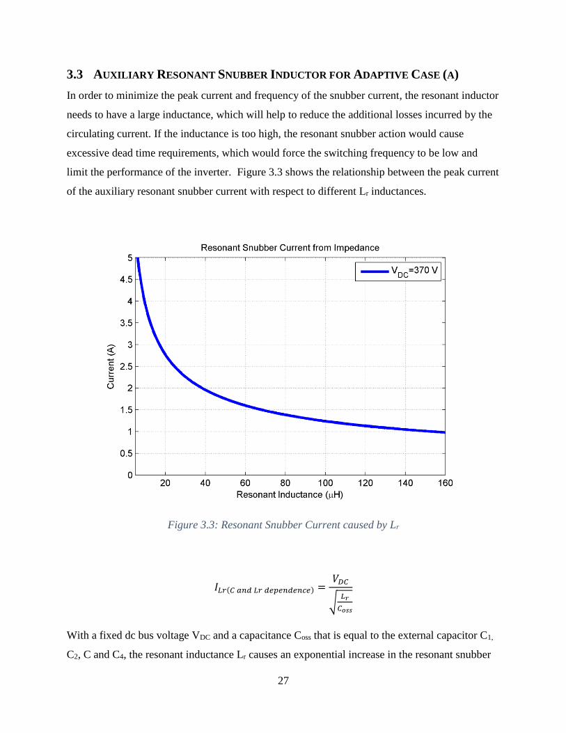
In order to minimize the peak current and frequency of the snubber current, the resonant inductor
needs to have a large inductance, which will help to reduce the additional losses incurred by the
circulating current. If the inductance is too high, the resonant snubber action would cause
excessive dead time requirements, which would force the switching frequency to be low and
limit the performance of the inverter. Figure 3.3 shows the relationship between the peak current
of the auxiliary resonant snubber current with respect to different Lr inductances.
Figure 3.3: Resonant Snubber Current caused by Lr
𝐼𝐿𝑟(𝐶 𝑎𝑛𝑑 𝐿𝑟 𝑑𝑒𝑝𝑒𝑛𝑑𝑒𝑛𝑐𝑒) =𝑉𝐷𝐶
√𝐿𝑟
𝐶𝑜𝑠𝑠
With a fixed dc bus voltage VDC and a capacitance Coss that is equal to the external capacitor C1,
C2, C and C4, the resonant inductance Lr causes an exponential increase in the resonant snubber
28
current ILr as the inductance is decreased. For lower inductances, there is a large change in peak
current for small changes in inductance, but the change in peak current decreases as the
inductance increases. Due to the adaptive control method for the auxiliary resonant snubber, the
inductance selected only needs to achieve ZVS for when the load current is below 0.5 A. When
the load current increases above 0.5 A, the turn on time tsn of the auxiliary resonant snubber will
be increased to turn on earlier, which will charge the resonant inductor enough to allow the
switches to still achieve ZVS.
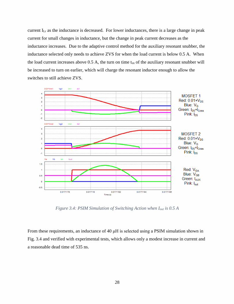
Figure 3.4: PSIM Simulation of Switching Action when Iout is 0.5 A
From these requirements, an inductance of 40 μH is selected using a PSIM simulation shown in
Fig. 3.4 and verified with experimental tests, which allows only a modest increase in current and
a reasonable dead time of 535 ns.

29
𝑓𝑠𝑛𝑢𝑏𝑏𝑒𝑟 =1
2𝜋√𝐿𝑟𝐶𝑜𝑠𝑠
The frequency of the current through the inductor fsnubber is inversely proportional to the values of
the resonant inductor and capacitor. With a capacitance of 1.12 nF and inductance of 40 μH, the
snubber resonant current frequency is about 750 kHz. From simulation, the peak resonant
current is 5 A and the RMS current is 0.63 A. To keep the losses of the inductor down while
maintaining a reasonable size, a RM8/I sized 3F35 core from Ferroxcube was chosen. In order
to give an inductance of 40 μH, 42 turns of 175/46 litz wire was used, which was achieved using
only half of the core.

30
3.4 ADAPTIVE AUXILIARY RESONANT SNUBBER CONTROL TIMING FOR
ADAPTIVE CASE (A)
With the large auxiliary inductor, the firing angle of the auxiliary resonant snubber has to be
modified if the load current is above 0.5 A in order to achieve ZVS. From the simulation results
shown in Fig. 3.5, it is shown that tsn has to be modified every 0.5 A.
Figure 3.5: PSIM Simulation of Switching Action for Adaptive Case (a) Control when Iout is 3.5
A
31
Table 3.2: Auxiliary Resonant Snubber Adaptive Timing for Adaptive Case (a)
Load Condition Simulation Turn
On Delay (tsn)
Experimental
Turn On Delay
(tsn)
0 A – 0.5 A 0 ns 60 ns
0.5 A – 1.0 A 60 ns 120 ns
1.0 A – 1.5 A 120 ns 180 ns
1.5 A – 2.0 A 190 ns 250 ns
2.0 A – 2.5 A 260 ns 310 ns
2.5 A – 3.0 A 340 ns 370 ns
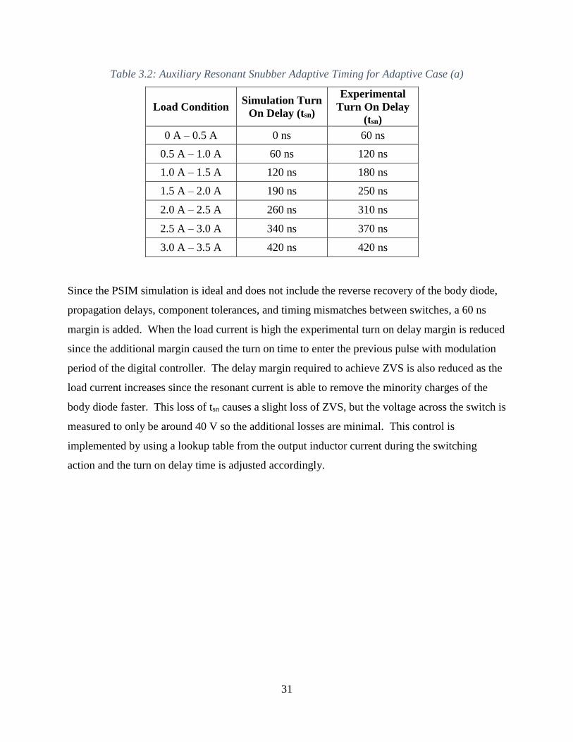
3.0 A – 3.5 A 420 ns 420 ns
Since the PSIM simulation is ideal and does not include the reverse recovery of the body diode,
propagation delays, component tolerances, and timing mismatches between switches, a 60 ns
margin is added. When the load current is high the experimental turn on delay margin is reduced
since the additional margin caused the turn on time to enter the previous pulse with modulation
period of the digital controller. The delay margin required to achieve ZVS is also reduced as the
load current increases since the resonant current is able to remove the minority charges of the
body diode faster. This loss of tsn causes a slight loss of ZVS, but the voltage across the switch is
measured to only be around 40 V so the additional losses are minimal. This control is
implemented by using a lookup table from the output inductor current during the switching
action and the turn on delay time is adjusted accordingly.

32
3.5 AUXILIARY RESONANT SNUBBER INDUCTOR FOR ADAPTIVE CASE (B)
To allow a fair comparison between adaptive case (a) and adaptive case (b), the same dead time
of 535 ns is used. From simulation, it is found that when the resonant inductance is 15 μH case
(b) works when tsn is equal to zero.
Figure 3.6: PSIM Simulation of Switching Action for Adaptive Case (b) Control when Iout is 3.5
A

33
Table 3.3: Auxiliary Resonant Snubber Adaptive Timing for Adaptive Case (b)
Load Condition Simulation Turn
On Delay (tsn)
Experimental
Turn On Delay
(tsn)
0 A- 0.5 A 130 ns 70 ns
0.5 A – 1 A 130 ns 70 ns
1.0 A -1.5 A 130 ns 70 ns
1.5 A – 2.0 A 100 ns 40 ns
2.0 A – 2.5 A 90 ns 30 ns
2.5 A – 3.0 A 70 ns 10 ns
3.0 A – 3.5 A 0 ns 0 ns
For currents below 3 A, tsn is adjusted to allow the ZVS window to occur without modifying the
dead time. To compensate for the reverse recovery of the body diode, a 60 ns margin is added.
As the load current reached its peak values the 60 ns margin was found to be excessive, so it was
reduced to allow the converter to achieve ZVS. Unlike the adaptive case (a) control, the
propagation delays, component tolerances, and timing mismatches cannot be compensated so
these variations can lead to a slight loss of ZVS.
3.6 AUXILIARY RESONANT SNUBBER SWITCH
In order to minimize the losses associated with the auxiliary branch and to operate with the high
frequency resonant currents, Gallium Nitride MOSFETs (GaN FETs) are selected as the
auxiliary resonant snubber. The switch needs to block the dc bus voltage, which creates a
specification for the maximum blocking voltage of 400 V. Due to the limited availability of high
voltage GaN FETs, Transphorm’s TPH3006 is selected.
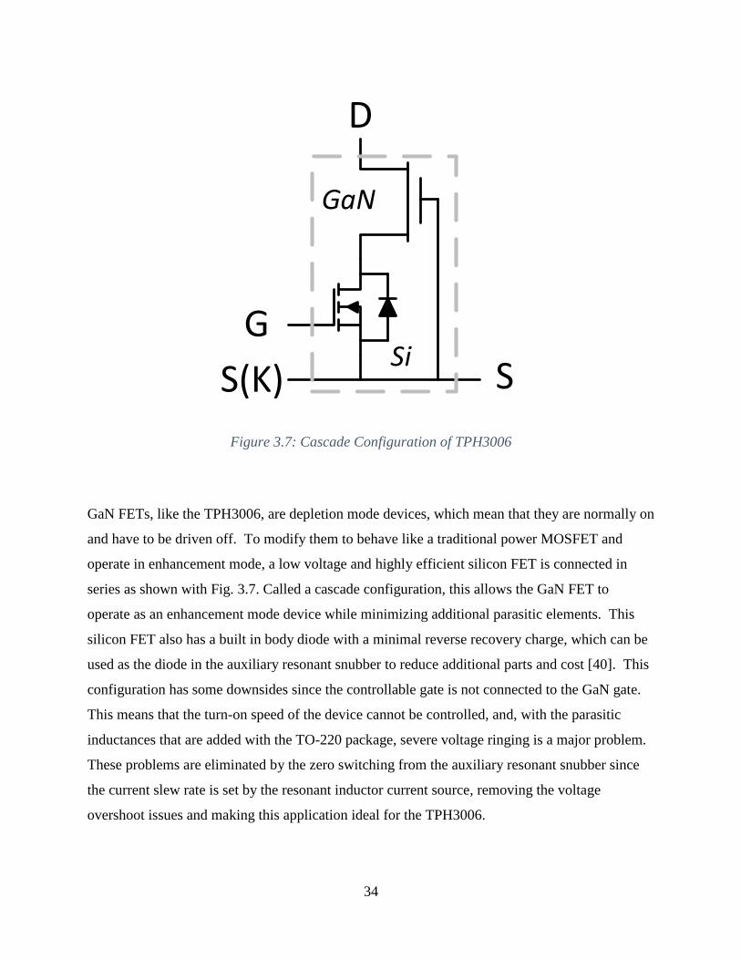
34
D
G
S(K) S
GaN
Si
Figure 3.7: Cascade Configuration of TPH3006
GaN FETs, like the TPH3006, are depletion mode devices, which mean that they are normally on
and have to be driven off. To modify them to behave like a traditional power MOSFET and
operate in enhancement mode, a low voltage and highly efficient silicon FET is connected in
series as shown with Fig. 3.7. Called a cascade configuration, this allows the GaN FET to
operate as an enhancement mode device while minimizing additional parasitic elements. This
silicon FET also has a built in body diode with a minimal reverse recovery charge, which can be
used as the diode in the auxiliary resonant snubber to reduce additional parts and cost [40]. This
configuration has some downsides since the controllable gate is not connected to the GaN gate.
This means that the turn-on speed of the device cannot be controlled, and, with the parasitic
inductances that are added with the TO-220 package, severe voltage ringing is a major problem.
These problems are eliminated by the zero switching from the auxiliary resonant snubber since
the current slew rate is set by the resonant inductor current source, removing the voltage
overshoot issues and making this application ideal for the TPH3006.

35
3.7 SWITCHING FREQUENCY
After selecting a dead time the switching frequency can be chosen. Since the switching losses are
eliminated, the switching frequency can be increased without significant additional losses, but
the conduction losses of the resonant snubber prevent the frequency from being increased too
high. The switching frequency was selected to be 40 kHz, which made the dead time equivalent
to 2.1% of the switching period. Once the design was finalized and experimental results were
run, the efficiency was found to decrease by 0.07% as the switching frequency was increased to
50 kHz, verifying the original design switching frequency as an optimal value.
3.8 DC BUS VOLTAGE
Once the switching frequency was set, the dc bus voltage could be specified. It is ideal to keep
the dc bus as low as possible, which will allow the modulation index and efficiency to be as high
as possible. From the PSIM simulation, it is found that the entire switching action requires a
worst case 915 ns for adaptive case (a) control.
𝐷𝑚𝑎𝑥 = 1 − 𝑡𝑑 𝑒𝑞𝑢𝑓𝑠𝑤
𝑉𝑜
𝑉𝑑𝑐= 𝑀 = 2𝐷𝑚𝑎𝑥 − 1
With a maximum equivalent dead time (td equ) equal to 915 ns, the minimum dc bus voltage that
can give a 240 Vrms output voltage is 366.2 V. In order to give an additional margin for voltage
drop from losses and approximations in the design model, the dc bus is selected to be 370 V.
This voltage is much higher than typical PV panel voltage, so the MPPT dc/dc stage will need to
boost the voltage.

36
3.9 OUTPUT FILTER
The output inductor has to filter out the switching noise on the output and keep the load current
relatively constant throughout the switching interval. By having a large inductance, the ripple
current will be minimized, which will decrease the core losses associated with the output
inductor. But in order to have a large inductance, a bulky core with many turns will be required,
causing the wire length, copper losses, size, and cost to all increase.
𝐿 =𝑉𝑑𝑐 − 𝑉𝑜
𝐼𝑜∆𝑖𝑇𝑠𝐷𝑚𝑎𝑥
To compare the tradeoff and improve the efficiency of the converter, two inductors were tested, a
1.76 mH which gave a 12% current ripple on the output inductor, and 0.88 mH, which gave a
24% current ripple. From an open loop experimental test, the circuit containing the 1.76 mH
inductor had 0.33% higher efficiency, so it was selected as the output inductor. In order to
minimize the losses, two RM14/I sized 3C95 cores from Ferroxcube were used. Each inductor
had 62 turns of 60/36 litz wire, which gave an inductance of 0.88 mH each to yield a 1.76 mH in
total when placed in series.
𝑓𝑐 =1
2𝜋√𝐿𝑜𝐶𝑜
In order to finalize the output filter design, the cut-off frequency of the second order low pass
output filter was set to be about 10 times lower than the switching frequency of 40 kHz. Based
on availability of high voltage film capacitors, 0.68 μF was selected, which gave a cutoff
frequency of 4.6 kHz.

37
3.10 DESIGN SUMMARY
The final list of parameters used in the resonant snubber inverter design is listed in Table 4. To
help filter out any potential input noise, a 2.2 μF film capacitor was placed on the input.
Table 3.4: Parameter Values from Design
Parameter
Value
Adaptive
Case (a)
Adaptive
Case (b)
Power Stage Switch IPB65R310CFD
External Capacitance 1.12 nF
Resonant Inductance 40 μH 15 μH
Auxiliary Switch TPH3006
Switching Frequency 40 kHz
Input DC Voltage 370 V
Output Inductance 1.76 mH
Output Capacitance 0.68 μF
Input Capacitance 2.2 μF
3.11 POWER STAGE HARDWARE TEST SETUP
In order to verify the design, a prototype 600 W resonant snubber inverter was built. To insure
that there would be no computation issues that would impact the performance of the inverter,
Texas Instrument’s TMS320F28335 32 bit floating point DSP was used as the controller.
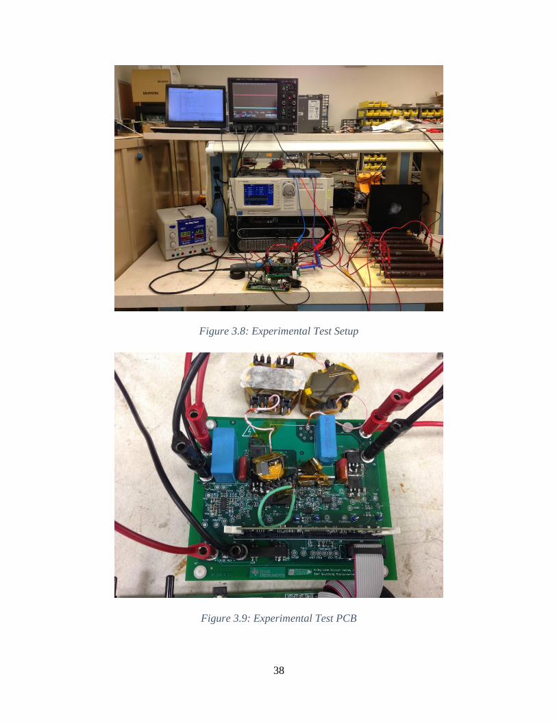
38
Figure 3.8: Experimental Test Setup
Figure 3.9: Experimental Test PCB

39
The dc bus voltage is supplied by two Sorensen power supplies, a 150 V XG 150-11.2 and a 330
V SGA330/15C-0AAA, that were connected in series to generate the required 370 V. The
control is powered by a 12 V auxiliary supply, a BK Precision 1672 power supply. The loads are
supplied by various FVT20020E250R0JE 250 Ω and 500 Ω 225 W power resistors from Vishay.
Since the input current has a significant double line frequency ripple that prevents simple
measurements, a Yokogawa WT1600 digital power meter is used to measure efficiency. The
oscilloscope waveforms are taken with a Teledyne LeCroy 104MXs-B Oscilloscope.
3.12 AUXILIARY VOLTAGE OVERSHOOT ISSUE
When the experimental test was first run, there was a significant voltage overshoot seen across
the drain to source of the auxiliary resonant snubber GaN FETs that prevented the input voltage
from reaching the designed value of 370 V. As the waveform shows in Fig. 3.10, when the
auxiliary resonant snubber switch turns off, a large ringing voltage occurs across the drain to
source of the GaN FET, which prevents the input voltage from reaching the design voltage of
370 V.
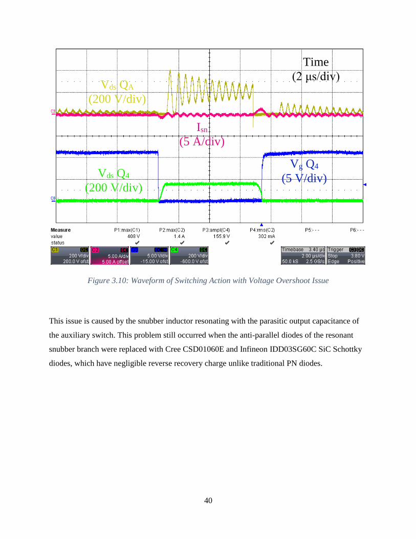
40
Figure 3.10: Waveform of Switching Action with Voltage Overshoot Issue
This issue is caused by the snubber inductor resonating with the parasitic output capacitance of
the auxiliary switch. This problem still occurred when the anti-parallel diodes of the resonant
snubber branch were replaced with Cree CSD01060E and Infineon IDD03SG60C SiC Schottky
diodes, which have negligible reverse recovery charge unlike traditional PN diodes.
Vg Q4
(5 V/div) Vds Q4
(200 V/div)
Isn
(5 A/div)
Vds QA
(200 V/div)
Time
(2 μs/div)

41
Figure 3.11: Waveform of Switching Action with Separate Resonant Snubber Legs
An attempt to remove the voltage overshoot issue by splitting the auxiliary resonant branch into
two independent legs was implemented, but this caused the parasitic capacitance to be equal to
the series connection of a GaN FET and SiC Schottky diode and significantly lower than the
original shared leg as shown in Fig. 3.11. While eliminating the voltage overshoot issue, the
diode allowed conduction in one direction but not the other. This caused the voltage across the
GaN FET to have a steady state voltage significantly higher than the dc bus, with the peak
voltage across the auxiliary branch equal to 459 V when the dc bus was only at 200 V. This
voltage increase prevented the inverter from operating at the designed dc bus value. With the
additional components required to implement this solution, it was found to not be an ideal
solution. To eliminate this problem, the original shared auxiliary leg with a clamping circuit to
eliminate the voltage overshoot is used instead.
Vg Q4
(5 V/div)
Vds Q4
(200 V/div)
Isn
(1 A/div) Vds QA
(200 V/div)
Time
(500 ns/div)
42
DC
Lo Ro
QBQA
Q1
Q2
Q3
Q4
CDC
C1 C3
C4C2
Lr
Co
Figure 3.12: Resonant Snubber Inverter with Clamping Diodes
The best way to eliminate the voltage overshoot problem was to place clamping diodes that
prevented the voltage across the switch from reaching voltages higher than the dc bus as shown
in Fig. 3.12. By circulating the energy until the power stage FETs switch again as opposed to
dissipating it, the clamping diodes are able to reduce the additional losses associated with
eliminating the voltage overshoot. Other attempts to limit the voltage such as RC (resistor and
capacitor), RCD (resistor, capacitor, and diode), and a saturable inductor placed across QA, QB,
and from the source of QA to ground and VDC had excessive losses that further hurt the efficiency
and caused hot spots that would limit the operating temperature range. Multiple diodes were
compared to find which one would be the best clamping diode with the goal to minimize
additional losses. After experimentally comparing Cree 2A CSD02060 and 20 A C4D20120A
SiC Schottky diodes against a traditional PN type NXP BYV29B ultrafast diode, the CSD02060
was found to give the inverter the highest measured efficiency so it was selected as the clamping
diode.
43
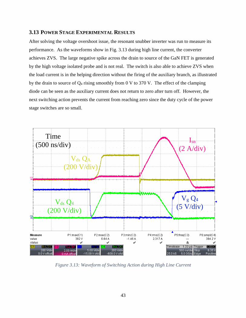
3.13 POWER STAGE EXPERIMENTAL RESULTS
After solving the voltage overshoot issue, the resonant snubber inverter was run to measure its
performance. As the waveforms show in Fig. 3.13 during high line current, the converter
achieves ZVS. The large negative spike across the drain to source of the GaN FET is generated
by the high voltage isolated probe and is not real. The switch is also able to achieve ZVS when
the load current is in the helping direction without the firing of the auxiliary branch, as illustrated
by the drain to source of Q4 rising smoothly from 0 V to 370 V. The effect of the clamping
diode can be seen as the auxiliary current does not return to zero after turn off. However, the
next switching action prevents the current from reaching zero since the duty cycle of the power
stage switches are so small.
Figure 3.13: Waveform of Switching Action during High Line Current
Vg Q4
(5 V/div) Vds Q4
(200 V/div)
Isn
(2 A/div)
Vds QA
(200 V/div)
Time
(500 ns/div)

44
As the waveforms show during low line current in Fig. 3.14, the converter fully achieves ZVS.
The noise generated by the switching action is significantly reduced since there is no ringing
across any of the devices observed when they change states. The effect of the clamping diode
over a longer period of time can be seen during this waveform, although the resonant snubber
current does not return to zero and the circulating energy slowly dissipating over time. This
additional current causes additional losses, which are further increased at smaller duty cycles
since there is more time for the current to circulate and energy dissipate through the loss
elements of the snubber and clamping circuitry.
Figure 3.14: Waveform of Switching Action during Low Line Current
Vg Q4
(5 V/div)
Vds Q4
(200 V/div)
Isn
(2 A/div)
Vds QA
(200 V/div)
Time
(2 μs/div)
45
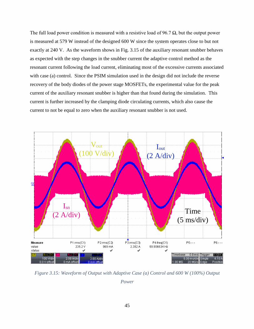
The full load power condition is measured with a resistive load of 96.7 Ω, but the output power
is measured at 579 W instead of the designed 600 W since the system operates close to but not
exactly at 240 V. As the waveform shows in Fig. 3.15 of the auxiliary resonant snubber behaves
as expected with the step changes in the snubber current the adaptive control method as the
resonant current following the load current, eliminating most of the excessive currents associated
with case (a) control. Since the PSIM simulation used in the design did not include the reverse
recovery of the body diodes of the power stage MOSFETs, the experimental value for the peak
current of the auxiliary resonant snubber is higher than that found during the simulation. This
current is further increased by the clamping diode circulating currents, which also cause the
current to not be equal to zero when the auxiliary resonant snubber is not used.
Figure 3.15: Waveform of Output with Adaptive Case (a) Control and 600 W (100%) Output
Power
Iout
(2 A/div)
Isn
(2 A/div)
Vout
(100 V/div)
Time
(5 ms/div)

46
The minimum power load of 10% is measured to compare the performance when the line current
is small. As the waveform in Fig. 3.16 shows, the adaptive control of the auxiliary resonant
snubber does not adjust to achieve ZVS since the load current never becomes too high. Since the
auxiliary resonant snubber inductor was sized to operate around this power level, the additional
losses are minimized, but this extra current will reduce the light load efficiency.
Figure 3.16: Waveform of Output with Adaptive Case (a) Control and60 W (10%) Output Power
Iout
(2 A/div)
Isn
(2 A/div)
Vout
(100 V/div)
Time
(5 ms/div)
47
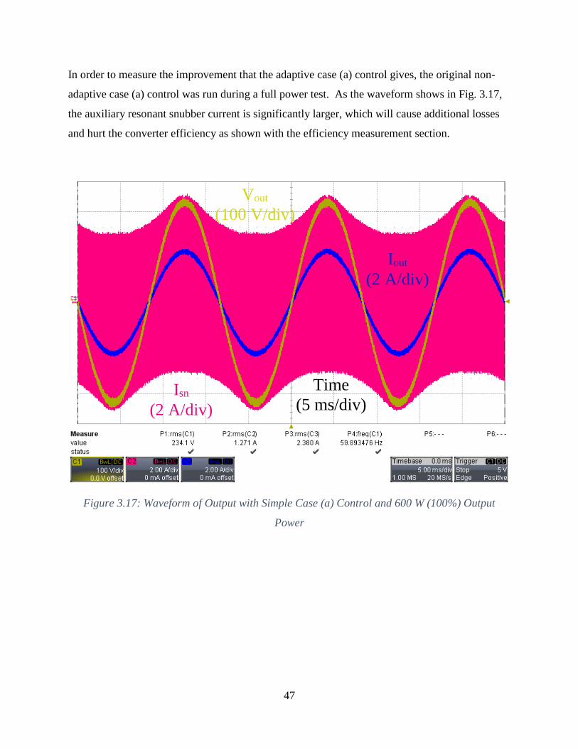
In order to measure the improvement that the adaptive case (a) control gives, the original non-
adaptive case (a) control was run during a full power test. As the waveform shows in Fig. 3.17,
the auxiliary resonant snubber current is significantly larger, which will cause additional losses
and hurt the converter efficiency as shown with the efficiency measurement section.
Figure 3.17: Waveform of Output with Simple Case (a) Control and 600 W (100%) Output
Power
Iout
(2 A/div)
Isn
(2 A/div)
Vout
(100 V/div)
Time
(5 ms/div)
48
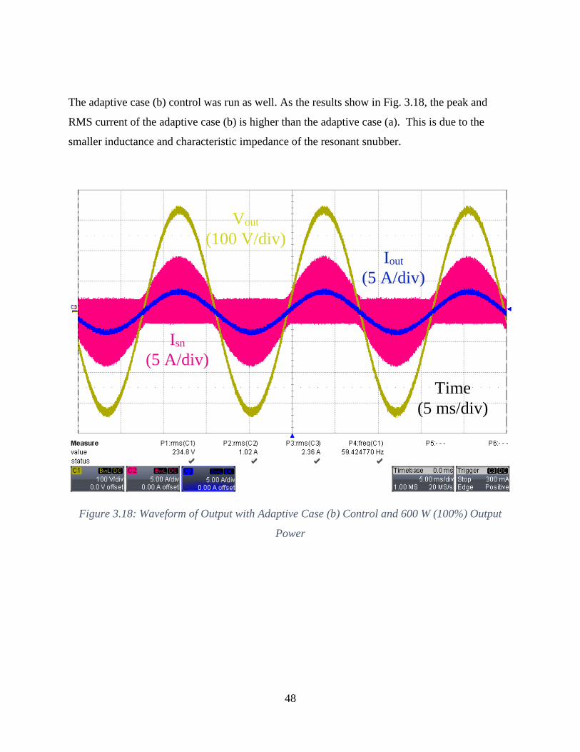
The adaptive case (b) control was run as well. As the results show in Fig. 3.18, the peak and
RMS current of the adaptive case (b) is higher than the adaptive case (a). This is due to the
smaller inductance and characteristic impedance of the resonant snubber.
Figure 3.18: Waveform of Output with Adaptive Case (b) Control and 600 W (100%) Output
Power
Iout
(5 A/div)
Isn
(5 A/div)
Vout
(100 V/div)
Time
(5 ms/div)

49
3.14 EFFICIENCY MEASUREMENT
The efficiency was measured using the Yokogawa WT1600 digital power meter, with the results
shown in Fig. 3.19. Adaptive case (a) and case (b) control efficiency are compared to one
another, as well as a non-adaptive case (a) control to allow the efficiency boost of the adaptive
control to be measured.
Figure 3.19: Measured Efficiency over CEC Operating Range
0.98160.98160.9799
0.9665
0.9561
0.9183
0.97970.97920.9754
0.9594
0.9479
0.9058
0.98110.98160.9796
0.9646
0.9553
0.9198
0.9
0.91
0.92
0.93
0.94
0.95
0.96
0.97
0.98
0.99
0 100 200 300 400 500 600
Eff
icie
ncy
Output Power (W)
Measured Efficiency
Adaptive Case (a)
Case (a)
Adaptive Case (b)

50
In order to easily compare the performance of the inverter over the entire operating region, the
California Energy Commission (CEC) efficiency is calculated, which is a weighted average of
the typical power level based on the power received by a solar installation in the Southwest
United States [41].
𝑛𝐶𝐸𝐶 = 0.04𝑛10% + 0.05𝑛20% + 0.12𝑛30% + 0.21𝑛50% + 0.53𝑛75% + 0.05𝑛100%
Since the exact power level for each weighted point could not be derived from the resistor bank,
there are some slight discrepancies between the ideal and measured output power. Using the test
protocol specifications for CEC efficiency measurements, all of the measured power levels are
within the allowed tolerance band so the average efficiency can be calculated.
Table 3.5: Ideal and Measured Output Power Levels
Power
Level
Ideal Output
Power
Measured
Output Power
Measured
Output Power
Level
Tolerance
100% 600 W 578.6 W 96.4% 95%-105%
75% 450 W 464.2 W 77.4% 70%-80%
50% 300 W 318.2 W 53.0% 45%-55%
30% 180 W 169.0 W 28.2% 27.5%-
32.5%
20% 120 W 118.2 W 19.7% 18%-22%
10% 60 W 59.6 W 9.9% 8%-10%
Table 3.6: Measured Efficiency of Various Control Methods
Control Method Peak Efficiency CEC Efficiency
Adaptive Case
(a) 98.16% 97.56%
Case (a) 97.97% 97.16%
Adaptive Case
(b) 98.16% 97.53%

51
As listed in Table 3.6, the efficiency of the microinverter operated in adaptive case (a). There is
a significant improvement in peak efficiency when adaptive case (a) is compared to the simple
case (a) control and there is a slight improvement in CEC efficiency for adaptive case (a) over
the adaptive case (b) control. Adaptive case (b) control has a large variation of auxiliary
resonant snubber timing to guarantee ZVS from small resonant inductor changes, which along
with the already small ZVS window that will make production of multiple units that perform
without a significant efficiency drop due to slight loss of ZVS difficult. Adaptive case (a) has a
much smaller variation on timing from component tolerance. With this simplification in
manufacturing and slightly higher CEC efficiency, adaptive case (a) is the best control method.
The CEC efficiency of 98.16% for case (a), which when compared to the peak efficiency of
95.6% for previous work with the resonant snubber inverter [38] is a significant improvement
but is still lower when compared to high efficiency hard switching topologies that are above 99%
[19]. Since the additional losses that the resonant snubber has are mostly dependent on the input
voltage, this causes a fixed loss that drastically hurts the light load power level. In order have a
system level CEC efficiency that is equivalent to the highest industry level of 96.5% for
microinverter applications [9], the dc/dc MPPT stage would have to have a CEC efficiency of
98.9%, which is currently unavailable for the high voltage gain required.
3.15 THERMAL MEASUREMENT LOSS ANALYSIS
The temperatures of the components that have large losses are measured with a Fluke Ti40FT
thermal imager to verify their performance at different power levels. The inverter is operating
with the adaptive case (a) control method and a fan used to prevent severe temperature rises.
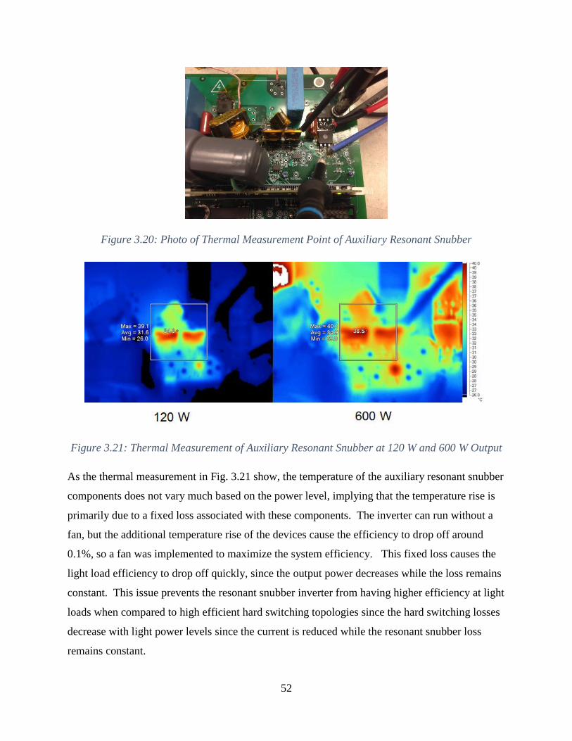
52
Figure 3.20: Photo of Thermal Measurement Point of Auxiliary Resonant Snubber
Figure 3.21: Thermal Measurement of Auxiliary Resonant Snubber at 120 W and 600 W Output
As the thermal measurement in Fig. 3.21 show, the temperature of the auxiliary resonant snubber
components does not vary much based on the power level, implying that the temperature rise is
primarily due to a fixed loss associated with these components. The inverter can run without a
fan, but the additional temperature rise of the devices cause the efficiency to drop off around
0.1%, so a fan was implemented to maximize the system efficiency. This fixed loss causes the
light load efficiency to drop off quickly, since the output power decreases while the loss remains
constant. This issue prevents the resonant snubber inverter from having higher efficiency at light
loads when compared to high efficient hard switching topologies since the hard switching losses
decrease with light power levels since the current is reduced while the resonant snubber loss
remains constant.
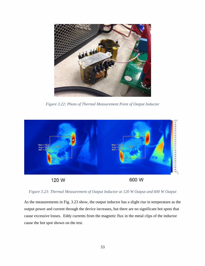
53
Figure 3.22: Photo of Thermal Measurement Point of Output Inductor
Figure 3.23: Thermal Measurement of Output Inductor at 120 W Output and 600 W Output
As the measurements in Fig. 3.23 show, the output inductor has a slight rise in temperature as the
output power and current through the device increases, but there are no significant hot spots that
cause excessive losses. Eddy currents from the magnetic flux in the metal clips of the inductor
cause the hot spot shown on the test.

54
Figure 3.24: Photo of Thermal Measurement Point of Power Stage Switches
Figure 3.25: Thermal Measurement of Power Stage Switches at 120 W Output and 600 W Output
As the thermal measurements in Fig. 3.25 show, the power stage switches have a large
temperature rise when the output power is increased. Due to the reverse recovery requirement of
the body diode, higher channel resistance MOSFETs had to be used, which limit the efficiency at
higher power levels.

55
From the thermal analysis, it can be seen that the resonant snubber causes the primary losses at
light power levels, but the power stage switches limit the efficiency as the power level is
increased to 600 W. With the devices and parameters selected, this gives a sweet spot of highest
efficiency around 500 W (Fig. 3.19), and, while performing better than previous resonant
snubber inverters, it has a lower efficiency than highly efficient hard switching topologies.

56
4 CONTROL
A large benefit of the resonant snubber inverter is that the zero voltage switching action does not
affect the plant duty cycle to output voltage and current plant transfer functions so the design of a
closed loop controlled system for standalone and grid tie applications is simple and easy to
implement.
4.1 STANDALONE MODE CONTROL
A standalone controller is needed if the solar panel installation is used in an application that
directly connects it to a specific load as opposed to a utility grid. This allows the inverter to
work in remote areas where a utility grid is not accessible, as well as serve as a backup generator
if there is a grid outage.
4.1.1 Standalone Mode Plant Model
Since the inverter is generating an ac voltage source, the control to output voltage (Gvd) transfer
function is required to allow the converter to regulate the output voltage.
𝐺𝑣𝑑 =𝑣𝑜
𝑑=
𝑉𝑑𝑐
1 + 𝑠𝐿𝑜
𝑅𝑜+ 𝑠2𝐿𝑜𝐶𝑜
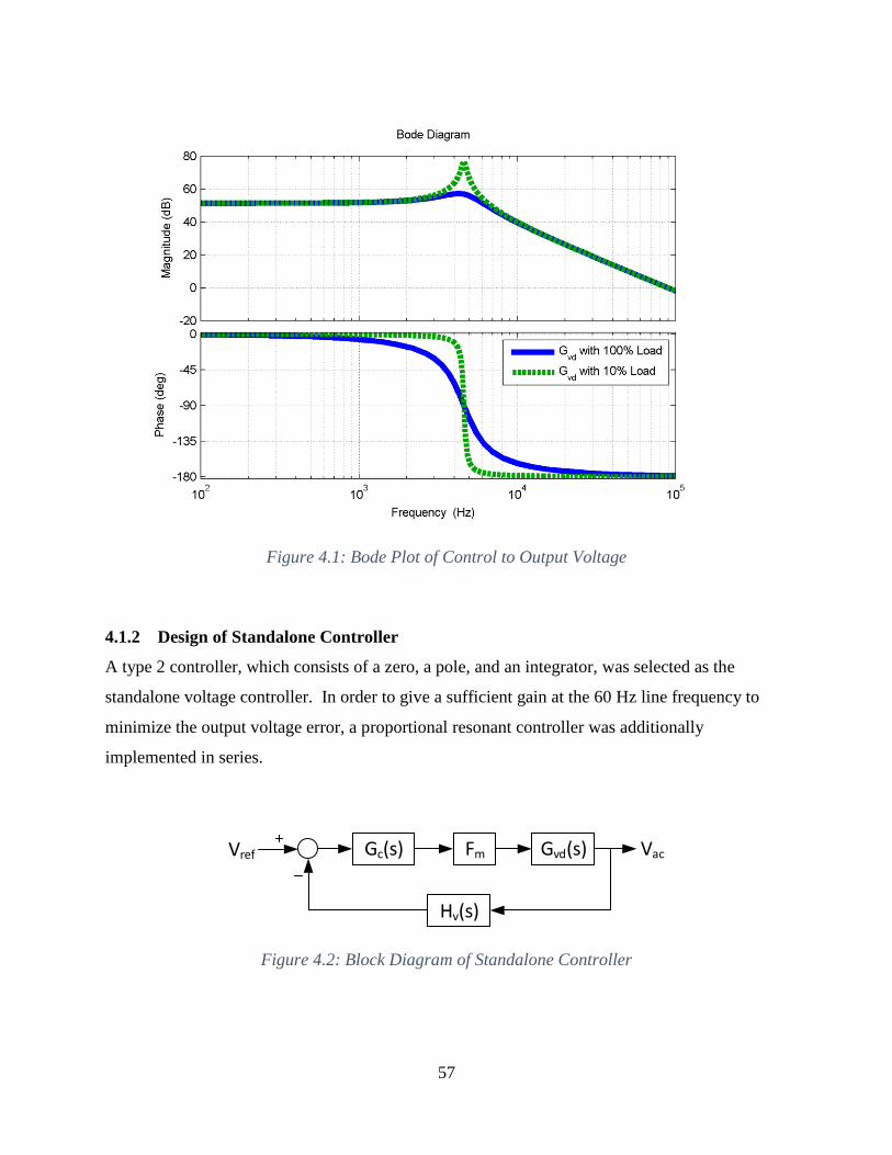
57
Figure 4.1: Bode Plot of Control to Output Voltage
4.1.2 Design of Standalone Controller
A type 2 controller, which consists of a zero, a pole, and an integrator, was selected as the
standalone voltage controller. In order to give a sufficient gain at the 60 Hz line frequency to
minimize the output voltage error, a proportional resonant controller was additionally
implemented in series.
Hv(s)
Vref Gc(s) Fm Gvd(s) Vac
Figure 4.2: Block Diagram of Standalone Controller
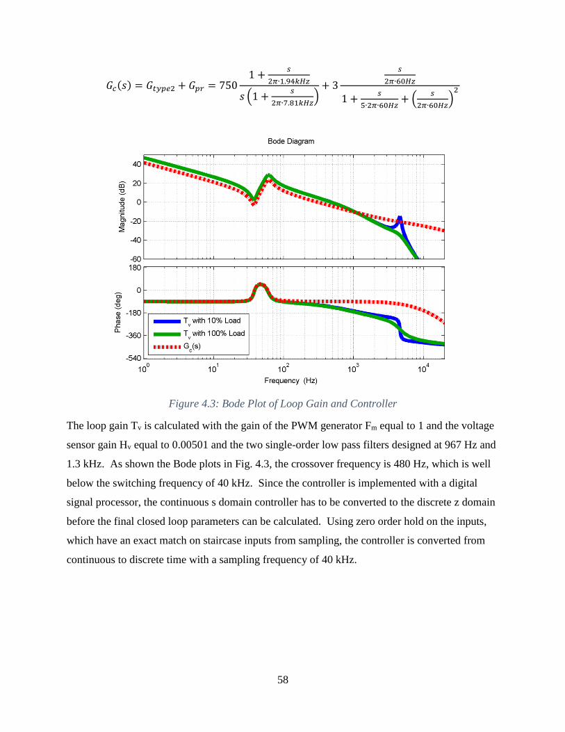
58
𝐺𝑐(𝑠) = 𝐺𝑡𝑦𝑝𝑒2 + 𝐺𝑝𝑟 = 7501 +
𝑠
2𝜋∙1.94𝑘𝐻𝑧
𝑠 (1 +𝑠
2𝜋∙7.81𝑘𝐻𝑧)
+ 3
𝑠
2𝜋∙60𝐻𝑧
1 +𝑠
5∙2𝜋∙60𝐻𝑧+ (
𝑠
2𝜋∙60𝐻𝑧)
2
Figure 4.3: Bode Plot of Loop Gain and Controller
The loop gain Tv is calculated with the gain of the PWM generator Fm equal to 1 and the voltage
sensor gain Hv equal to 0.00501 and the two single-order low pass filters designed at 967 Hz and
1.3 kHz. As shown the Bode plots in Fig. 4.3, the crossover frequency is 480 Hz, which is well
below the switching frequency of 40 kHz. Since the controller is implemented with a digital
signal processor, the continuous s domain controller has to be converted to the discrete z domain
before the final closed loop parameters can be calculated. Using zero order hold on the inputs,
which have an exact match on staircase inputs from sampling, the controller is converted from
continuous to discrete time with a sampling frequency of 40 kHz.

59
Figure 4.4: Comparison between Continuous and Discrete Time Domain of Standalone
Controller
𝐺𝑐(𝑧) = 𝐺𝑡𝑦𝑝𝑒2(𝑧) + 𝐺𝑝𝑟(𝑧) =0.05143 𝑧−1 − 0.03818 𝑧−2
1 − 1.293 𝑧−1 + 0.2932 𝑧−2+
0.02825 𝑧−1 − 0.02825 𝑧−2
1 − 1.998 𝑧−1 + 0.9981 𝑧−2
As the conversion shows in Fig. 4.4, the continuous and discrete controller around and below the
crossover frequency of 480 Hz is equal. The system is still guaranteed to be stable as the
sampling delay at 40 kHz is sufficiently far away from the crossover frequency.
Table 4.1: Standalone Closed Loop Operating Parameters
Parameter Tv with 10% Load Tv with 100% Load
fc 481 Hz 480 Hz
Φm 48.4° 45.5°
Gm 14.4 dB 12 dB
60 Hz Gain 28.6 dB 28.8 dB

60
As the final parameters in Table 4.1 show, the system is stable with large safety margins. With a
60 Hz gain of 28.6 dB and 28.8 dB for a 10% load and 100% load, respectively, the steady state
line frequency error will be about 3.6%, which is a reasonable error for a utility scale voltage
source application.
4.1.3 Simulation of Standalone Controller
The controller design was verified in PSIM with the steady state and dynamic from 10% to 100%
load step performance measured. The worst case response occurs when the load steps from full
load to minimum load as the simulation results show in Fig. 4.5 and Fig. 4.6, and as the
simulation shows the converter is stable.
Figure 4.5: PSIM Simulation of Output Waveforms
0
-200
-400
200
400
Vout
0.1 0.12 0.14 0.16 0.18 0.2
Time (s)
0
-2
-4
2
4
Iout
Iout
Vout

61
Figure 4.6: PSIM Simulation of 100% to 10% Load Step
Table 4.2: Standalone Controller Steady State Simulation Results
Parameter Steady State 10%
Load Response
Steady State 100%
Load Response
Vout 232 Vrms 232 Vrms
Output Voltage THD 2.2% 2.2%
Output Current THD 2.2% 2.2%
Table 4.3: Standalone Controller Dynamic Simulation Results
Parameter Step Up 10% to
100% Load Response
Step Down 10% to
100% Load Response
Vpeak 363 V 478 V
Overshoot 10% 44%
Settling Time 0.2 ms 0.7 ms
The controller allows the inverter to operate within the design parameters without any problems.
While the voltage overshoot for the step down response is slightly large this overshoot behaves
like a voltage spike that are caused by surges in the utility grid due to the inverter’s quick
response. Since loads connected to the output of the inverter are designed to run off the grid, this
voltage overshoot will not cause any problems.
200
250
300
350
400
450
Vout
0.154 0.1545 0.155 0.1555 0.156
Time (s)
0
0.5
1
1.5
2
2.5
3
3.5
Iout
Iout
Vout

62
4.1.4 Experimental Results of Standalone Controller
To verify the design, the standalone controller was implemented with the 600 W prototype. The
control was implemented with a Texas Instruments TMS320F28335 DSP. Due to offsets in the
output voltage sensing the output voltage was regulated at 222 Vrms when the reference voltage
in the controller was set to 240 Vrms. To compensate for this error, the reference voltage was
increased to 255 Vrms. The total harmonic distortion was measured with a Fluke 43B Power
Quality Analyzer.
Figure 4.7: Waveform of Output with Standalone Control
Table 4.4: Measured Steady State Operating Parameters
Parameter Steady State 20%
Load Response
Steady State 100%
Load Response
Vout 236.5 Vrms 237.4 Vrms
Output Voltage THD 3.0% 2.8%
Output Current THD 2.9% 2.8%
Vout
(100 V/div)
Iout
(2 A/div) Time
(5 ms/div)
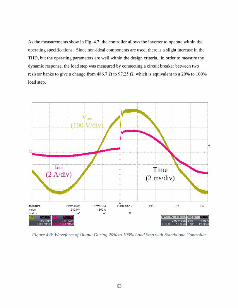
63
As the measurements show in Fig. 4.7, the controller allows the inverter to operate within the
operating specifications. Since non-ideal components are used, there is a slight increase in the
THD, but the operating parameters are well within the design criteria. In order to measure the
dynamic response, the load step was measured by connecting a circuit breaker between two
resistor banks to give a change from 486.7 Ω to 97.25 Ω, which is equivalent to a 20% to 100%
load step.
Figure 4.8: Waveform of Output During 20% to 100% Load Step with Standalone Controller
Vout
(100 V/div)
Iout
(2 A/div) Time
(2 ms/div)
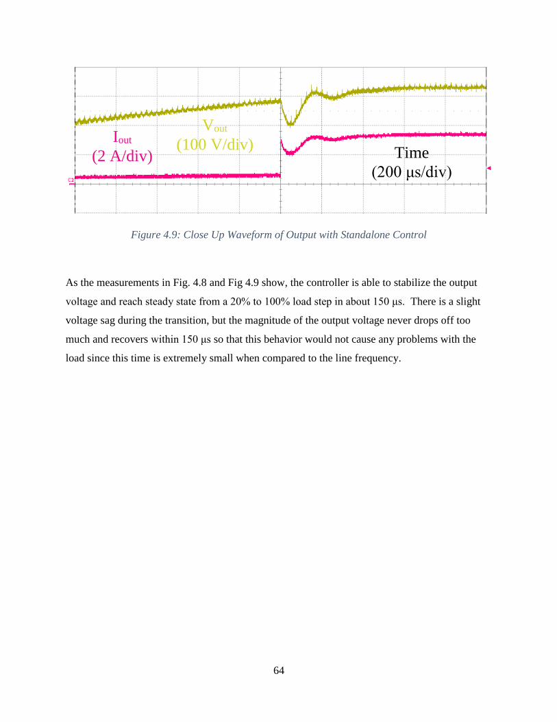
64
Figure 4.9: Close Up Waveform of Output with Standalone Control
As the measurements in Fig. 4.8 and Fig 4.9 show, the controller is able to stabilize the output
voltage and reach steady state from a 20% to 100% load step in about 150 μs. There is a slight
voltage sag during the transition, but the magnitude of the output voltage never drops off too
much and recovers within 150 μs so that this behavior would not cause any problems with the
load since this time is extremely small when compared to the line frequency.
Vout
(100 V/div) Iout
(2 A/div) Time
(200 μs/div)

65
4.2 GRID TIE CONTROL
The most popular use for solar panel inverters is to convert the generated energy from the PV to
tie into the existing utility grid and to power various electrical devices that connected to the grid
or directly to the PV inverter. For residential applications, the solar-generated energy can be
used to reduce or even eliminate power bought from the utility. To deliver power to the grid,
certain standards need to be met to keep the power quality high and safe, which require a more
stringent controller as well as a need to protect the inverter from being damaged by the transients
from the grid. In order to allow the output current to satisfy the THD requirements of IEEE Std.
1547, a smaller second inductor Lg is added after the output capacitor to further filter the output
current. If the required inductance of Lg is small enough it can be implemented with the leakage
inductance of the utility transformer and inductance of the utility wire instead of an additional
component, preventing any additional cost. An external resistor is connected in series with the
capacitor to dampen the peaking effect it has on the control transfer functions, which left
undamped prevent the converter from stabilizing. These changes to the inverter are shown in
Fig. 4.10.
Figure 4.10: Schematic of Grid Tie Resonant Snubber Inverter
DC
Lo
QBQA
Q1
Q2
Q3
Q4
CDC
C1
Lr
C3
C4C2
Co
Lg
AC
+
vac
-
iac ig
ESR

66
4.2.1 Phase Lock Loop
Before the grid tie controller can be designed, a phase lock loop needs to be designed to allow
the controller to synchronize with the grid line frequency. This is achieved with a simple phase
locked loop, with the sinusoidal output used to generate the reference current for the current loop
controller.
Vgrid LPF Kp
ω=2πf
1/s cos(θ)
sin(θ) Vsync
Figure 4.11: Block Diagram of Phase Locked Loop
Figure 4.12: Loop Gain of Phase Locked Loop

67
By using a second order low pass filter (LPF) with a cutoff frequency of 20 Hz and a damping
ratio of 0.7 along with a gain Kp of 60, the crossover frequency is found to be at 9.37 Hz with a
phase margin is 50° and a gain margin of 9.34 dB. To verify the design, the phase locked loop is
simulated in PSIM.
Figure 4.13: PSIM Simulation of Phase Locked Loop (Red: Input, Blue: Output)
As the simulation results in Fig. 4.13 show, the output synchronizes to the input frequency within
0.2 sunder a worst case of a 180° input phase shift. In order to prevent problems with startup,
the controller will have a delay longer than the synchronization time before gating occurs to
allow the phase lock loop to properly lock to the grid frequency.
4.2.2 Grid Tie Plant Model
Since the output voltage is set by the utility grid, the output current is controlled by the inverter,
which requires the control to output current (Gid) transfer function to design a proper controller.
Before Gid can be derived, the output current sensor location needs to be selected since the plant
can dramatically change based on its location. To allow the inverter to work interchangeably
between standalone and grid tie mode, the output voltage and current sensors are left in the same
place of across the output capacitor and through Lo. With this current sense location, the plant
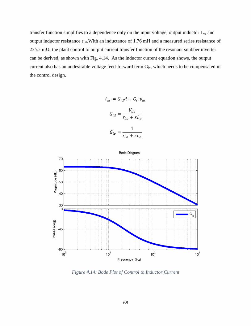
68
transfer function simplifies to a dependence only on the input voltage, output inductor Lo, and
output inductor resistance rLo.With an inductance of 1.76 mH and a measured series resistance of
255.5 mΩ, the plant control to output current transfer function of the resonant snubber inverter
can be derived, as shown with Fig. 4.14. As the inductor current equation shows, the output
current also has an undesirable voltage feed-forward term Giv, which needs to be compensated in
the control design.
𝑖𝑎𝑐 = 𝐺𝑖𝑑𝑑 + 𝐺𝑖𝑣𝑣𝑎𝑐
𝐺𝑖𝑑 =𝑉𝑑𝑐
𝑟𝐿𝑜 + 𝑠𝐿𝑜
𝐺𝑖𝑣 =1
𝑟𝐿𝑜 + 𝑠𝐿𝑜
Figure 4.14: Bode Plot of Control to Inductor Current

69
4.2.3 Control Block Diagram
To design the compensators for the current loop and undesirable feed-forward term, the control
structure needs to be defined. By carefully placing their location as shown in Figure 4.15 the
plant model Gid can be simplified for simple compensator design and Giv can be reduced to a
constant scalar value independent of any dynamic term.
vac Hv/PLL
kxIref
Gi
Hi
Fm Gid
iac
Giv
ig
sCo
Gc
Figure 4.15: Grid Tie Control Block Diagram
The current loop is dependent on Fm, Gid, Hi, and is compensated with Gi. To compensate for the
feed-forward term, Gc is used to eliminate its effect on the output. To eliminate instability issues
that arise from the zero in the capacitor feed-forward term, an external resistor of 3.3 Ω is placed
in series of the output capacitor to increase the equivalent series resistance. Since the ripple
current through the capacitor is small, the additional losses associated by adding a resistive
element are minimal.
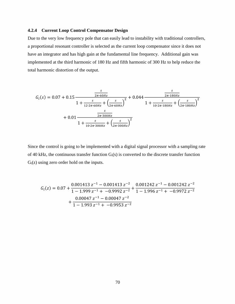
70
4.2.4 Current Loop Control Compensator Design
Due to the very low frequency pole that can easily lead to instability with traditional controllers,
a proportional resonant controller is selected as the current loop compensator since it does not
have an integrator and has high gain at the fundamental line frequency. Additional gain was
implemented at the third harmonic of 180 Hz and fifth harmonic of 300 Hz to help reduce the
total harmonic distortion of the output.
𝐺𝑖(𝑠) = 0.07 + 0.15
𝑠
2𝜋∙60𝐻𝑧
1 +𝑠
12∙2𝜋∙60𝐻𝑧+ (
𝑠
2𝜋∙60𝐻𝑧)
2 + 0.044
𝑠
2𝜋∙180𝐻𝑧
1 +𝑠
10∙2𝜋∙180𝐻𝑧+ (
𝑠
2𝜋∙180𝐻𝑧)
2
+ 0.01
𝑠
2𝜋∙300𝐻𝑧
1 +𝑠
10∙2𝜋∙300𝐻𝑧+ (
𝑠
2𝜋∙300𝐻𝑧)
2
Since the control is going to be implemented with a digital signal processor with a sampling rate
of 40 kHz, the continuous transfer function Gi(s) is converted to the discrete transfer function
Gi(z) using zero order hold on the inputs.
𝐺𝑖(𝑧) = 0.07 +0.001413 𝑧−1 − 0.001413 𝑧−2
1 − 1.999 𝑧−1 + −0.9992 𝑧−2+
0.001242 𝑧−1 − 0.001242 𝑧−2
1 − 1.996 𝑧−1 + −0.9972 𝑧−2
+0.00047 𝑧−1 − 0.00047 𝑧−2
1 − 1.993 𝑧−1 + −0.9953 𝑧−2
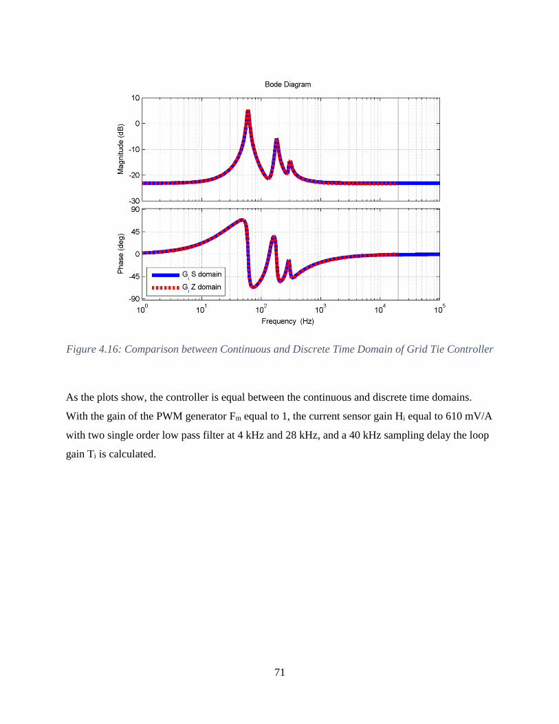
71
Figure 4.16: Comparison between Continuous and Discrete Time Domain of Grid Tie Controller
As the plots show, the controller is equal between the continuous and discrete time domains.
With the gain of the PWM generator Fm equal to 1, the current sensor gain Hi equal to 610 mV/A
with two single order low pass filter at 4 kHz and 28 kHz, and a 40 kHz sampling delay the loop
gain Ti is calculated.
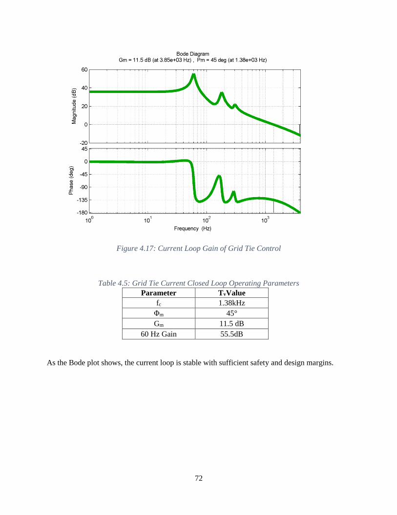
72
Figure 4.17: Current Loop Gain of Grid Tie Control
Table 4.5: Grid Tie Current Closed Loop Operating Parameters
Parameter TvValue
fc 1.38kHz
Φm 45°
Gm 11.5 dB
60 Hz Gain 55.5dB
As the Bode plot shows, the current loop is stable with sufficient safety and design margins.

73
4.2.5 Feed Forward Compensator Design
In order to eliminate the undesired feed-forward term Giv, a compensator Gc is implemented. By
sensing vac and adding the compensation after the current loop compensator as shown in the grid
tie control block diagram in Figure 55, this term can be reduced to constants and easily be
implemented [42]. Since the crossover frequency of the current loop controller is much lower
than the low pass filter of the ac voltage sensor Hv, the gain can be approximated as the passband
value.
𝐺𝑐 =1
𝐻𝑣𝑉𝑑𝑐𝐹𝑚
4.2.6 Simulation of Grid Tie Controller
The complete grid tie control was verified with a PSIM simulation as shown in Figure 4.18. The
voltage across the output capacitor vac, sensed current iac, and load current ig are measured.
Figure 4.18: PSIM Simulation of Grid Tie Control under Full Load
Ig
Vac
Iac

74
As the output waveforms show, the controller is stable and current is able to track the output
voltage and deliver power to the grid. In order for grid connected inverters to be allowed to
connect to the utility grid, they need to meet the IEEE Standard 1547 for interconnecting
distributed resources with electric power systems. One parameter that is specified and has a
large impact on the control design is the maximum total demand distortion (TDD), which is a
measurement of the total harmonic distortion of the output based in percent of the full load
fundamental current [43].
Table 4.6: Maximum Harmonic Current Distortion in Percent of Current from IEEE Std. 1547
Individual
Harmonic
Order
h < 11 11 ≤ h 17 17 ≤ h 23 23 ≤ h 35 35 ≤ h
Total
Demand
Distortion
Percent (%) 4.0 2.0 1.5 0.6 0.3 5.0
To meet these harmonic requirements with the existing controller, the additional inductor Lg is
set to 0.25 mH. With this additional inductance, the simulated current THD for full load is
measured to be 3.4%, which satisfies the standards requirement.
𝑇𝐷𝐷 =√𝐼ℎ𝑎𝑟𝑚𝑜𝑛𝑖𝑐 2
2 + 𝐼ℎ𝑎𝑟𝑚𝑜𝑛𝑖𝑐 32 + 𝐼ℎ𝑎𝑟𝑚𝑜𝑛𝑖𝑐 4
2 + 𝐼ℎ𝑎𝑟𝑚𝑜𝑛𝑖𝑐 52 + ⋯
𝐼𝐿
Even though the THD of the output current increases as the power level decreases with 15.4%
current THD for 20% power level, the TDD is only 3.5% and remains under the limits since the
harmonic content is measured with respect to the full load IL as opposed to the fundamental of
the individual power levels.
4.2.7 Experimental Results of Grid Tie Controller
To experimentally verify the grid tie control, the inverter was connected to the utility grid using a
2 kVA Square D transformer to step up the 120 V voltage to 240 V. The leakage inductance of

75
the transformer on the inverter side is measured to be 2.65 mH, which increases Lg and allows
the inductance to be much larger than the simulation value without adding any additional
components. Since the grid voltage has low frequency harmonics that do not appear in the
simulation, the controller gains were modified to allow the output current to meet the IEEE Std.
1547 TDD limits. Since these larger gains reduce the phase and gain margin, they were
incrementally adjusted to insure that the system would not become unstable. The controller was
able to be experimentally verified, with the output waveforms show in Fig. 4.19.
𝐺𝑖(𝑠) = 0.23 + 0.1
𝑠
2𝜋∙60𝐻𝑧
1 +𝑠
10∙2𝜋∙60𝐻𝑧+ (
𝑠
2𝜋∙60𝐻𝑧)
2 + 0.09
𝑠
2𝜋∙180𝐻𝑧
1 +𝑠
8∙2𝜋∙180𝐻𝑧+ (
𝑠
2𝜋∙180𝐻𝑧)
2
+ 0.03
𝑠
2𝜋∙300𝐻𝑧
1 +𝑠
8∙2𝜋∙300𝐻𝑧+ (
𝑠
2𝜋∙300𝐻𝑧)
2
𝐺𝑖(𝑧) = 0.23 +0.000942 𝑧−1 − 0.000942 𝑧−2
1 − 1.999 𝑧−1 + −0.9991 𝑧−2+
0.00254 𝑧−1 − 0.00254 𝑧−2
1 − 1.996 𝑧−1 + −0.9965 𝑧−2
+0.001409 𝑧−1 − 0.001409 𝑧−2
1 − 1.992 𝑧−1 + −0.9941 𝑧−2
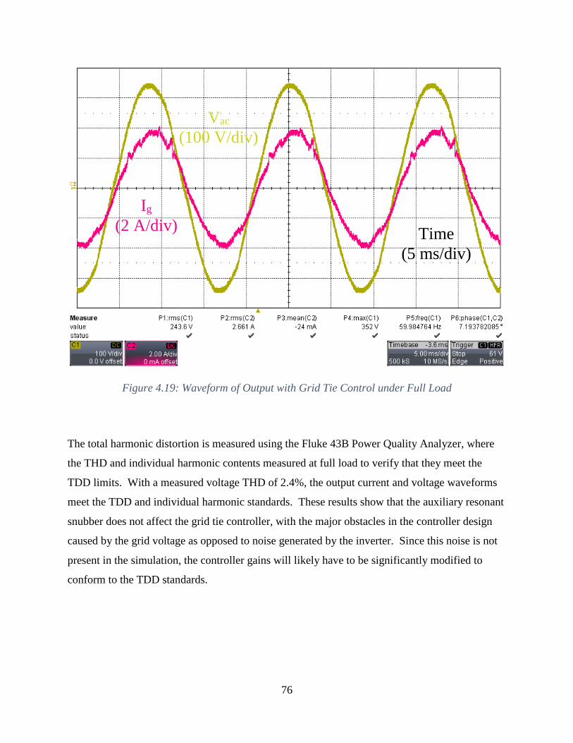
76
Figure 4.19: Waveform of Output with Grid Tie Control under Full Load
The total harmonic distortion is measured using the Fluke 43B Power Quality Analyzer, where
the THD and individual harmonic contents measured at full load to verify that they meet the
TDD limits. With a measured voltage THD of 2.4%, the output current and voltage waveforms
meet the TDD and individual harmonic standards. These results show that the auxiliary resonant
snubber does not affect the grid tie controller, with the major obstacles in the controller design
caused by the grid voltage as opposed to noise generated by the inverter. Since this noise is not
present in the simulation, the controller gains will likely have to be significantly modified to
conform to the TDD standards.
Vac
(100 V/div)
Ig
(2 A/div) Time
(5 ms/div)

77
Table 4.7: Harmonic Content of Grid Tie Output Current under Full Load
Harmonic Percent Harmonic Percent
Ig THD 4.6% 9 0.1%
2 1.0% 10 0.4%
3 2.6% 11 0.4%
4 0.8% 12 0.5%
5 1.4% 13 1.8%
6 0.3% 14 0.5%
7 1.6% 15 0.0%
8 0.2% 16 0.5%

78
5 CONCLUSION
As highlighted in the design and demonstrated with the experimental test PCB, the resonant
snubber inverter (RSI) is able to achieve a much higher efficiency than previous resonant
snubber inverter designs while minimizing additional parts, maintaining simple control, and
eliminating electrical noise. With only four additional capacitors, one resonant inductor, and two
auxiliary switches, the additional parts and size increase compared to the traditional hard
switching inverter are minimal. These components are not in the power stage path so they can be
small and cheap, especially when compared to the size and cost of the additional components
that are required in high efficiency hard switching inverters. Currently, GaN devices are more
expensive than their Si counterparts since GaN is a new semiconductor material for high voltage
field effect transistors, but, as their cost decreases over time as fabrication processes improve, the
cost of the components for the resonant snubber inverter will reduce further. The efficiency of
the inverter is improved without any additional parts by utilizing the output current sensor, which
is required for closed loop control since the converter is able to achieve soft switching over the
entire line cycle despite the moving ZVS window without any additional circuitry or elements.
By taking advantage of the bipolar switching, the lower frequency harmonics and common mode
noise generated by the converter are naturally eliminated, which, along with the higher switching
frequency that is allowed by the soft switching, allows the output filter to easily meet the output
waveform distortion requirements.
Despite all of these benefits, there were still some drawbacks with the improved resonant
snubber inverter. When compared to high efficiency hard switching inverters, the resonant
snubber inverter is still less efficient. From the loss analysis, it is shown that the losses of the
auxiliary resonant snubber are largely independent of the power level, which causes the
efficiency to drop off at light load. As the power level increases, the losses associated with the
higher channel resistance of the fast body diode MOSFETs cause the efficiency to peak at levels
below the maximum of other topologies that are able to use lower on-state resistance switches.
The circulating currents caused by the diode clamp further reduce the efficiency of the resonant
snubber inverter.

79
From the experimental results of a 600 W prototype a peak efficiency of 98.16% and CEC
efficiency of 97.56% was measured, with a worst case THD of 3.0% for the output voltage
during a standalone test and 4.6% TDD for the output current during a grid tie test.
5.1 FUTURE WORK
While many improvements have been made on the resonant snubber inverter, there are still some
drawbacks that limit its performance. There are several directions for future research on the
resonant snubber inverter to improve over these issues.
Replace the power stage switches with newer generations of fast body diode switches that
have smaller channel resistances
Replace the auxiliary resonant snubber switches with newer generations of GaN FETs
that have smaller channel resistances and smaller output capacitances, reducing and
possibly eliminating the voltage overshoot and clamping diode losses.
Detailed analysis of external capacitance effect on tradeoff between turn-off loss and
resonant snubber loss to determine an optimal value.
80
REFERENCES
[1] Massachusetts Clean Energy Center. (2014, January 7). Solarize Mass. Available:
http://www.masscec.com/solarizemass
[2] California Energy Commision, State of California, & California Public Utilities
Commission. (2014, January 7). Go Solar California. Available:
http://www.gosolarcalifornia.ca.gov/
[3] N. Sridhar. (2011, January 7 2014). Understanding Photovoltaics and the Market Forces
Behind Them. Available: http://www.ti.com/lit/an/slva448/slva448.pdf
[4] Texas Instruments. (2011, January 7 2014). Energy Harvesting: Solar. Available:
http://www.ti.com/lit/sl/slyy027/slyy027.pdf
[5] Power-One, "UNO-2.0-I UNO-2.5-I," Datasheet, Ed., 2013-04.1 ed, 2014.
[6] SMA, "Sunny Boy 6000TL-US/7000TL-US/8000TL-US/9000TL-US/10000TL-US,"
Datasheet, Ed., 1.3 ed. Online, 2013.
[7] Power-One, "Micro-0.25-I Micro-0.3-I," Datasheet, Ed., 2013-03.8 ed, 2014.
[8] SolarBridge Technologies, "Pantheon II Integrated Microinverter," Datasheet, Ed., 1 ed,
2014.
[9] Enphase, "Enphase M250," Datasheet, Ed., 1 ed. Online, 2014.
[10] Texas Instruments. (2010, January 7 2014). AN-2122 SM3320-RF-EV Reference Design.
Available: http://www.ti.com/lit/an/snosb82e/snosb82e.pdf
[11] Z. Huiying, L. Shuhui, and J. Proano, "PV energy extraction characteristic study under
shading conditions for different converter configurations," in Power and Energy Society
General Meeting, 2012 IEEE, 2012, pp. 1-8.
[12] S. V. Dhople, J. L. Ehlmann, A. Davoudi, and P. L. Chapman, "Multiple-input boost
converter to minimize power losses due to partial shading in photovoltaic modules," in
Energy Conversion Congress and Exposition (ECCE), 2010 IEEE, 2010, pp. 2633-2636.
[13] S. V. Araujo, P. Zacharias, and R. Mallwitz, "Highly Efficient Single-Phase
Transformerless Inverters for Grid-Connected Photovoltaic Systems," Industrial
Electronics, IEEE Transactions on, vol. 57, pp. 3118-3128, 2010.
[14] P. Sun, C. Liu, J.-S. Lai, and C.-L. Chen, "Cascade Dual Buck Inverter With Phase-Shift
Control," Power Electronics, IEEE Transactions on, vol. 27, pp. 2067-2077, 2012.
[15] M. Victor, F. Greizer, S. Bremicker, and U. Hübler, "Method of converting a direct
current voltage from a source of direct current voltage, more specifically from a
photovoltaic source of direct current voltage, into a alternating current voltage," US
Patent 7411802, 2008.
[16] W. Yu, J.-S. Lai, H. Qian, and C. Hutchens, "High-Efficiency MOSFET Inverter with
H6-Type Configuration for Photovoltaic Nonisolated AC-Module Applications," Power
Electronics, IEEE Transactions on, vol. 26, pp. 1253-1260, 2011.
[17] G. Bin, J. Dominic, J.-S. Lai, C.-L. Chen, T. LaBella, and B. Chen, "High Reliability and
Efficiency Single-Phase Transformerless Inverter for Grid-Connected Photovoltaic
Systems," Power Electronics, IEEE Transactions on, vol. 28, pp. 2235-2245, 2013.
[18] H. Schmidt, C. Siedle, and J. Ketterer, "DC/AC converter to convert direct electric
voltage into alternating voltage or into alternating current," US Patent 7,046,534, 2006.
[19] B. Burger and D. Kranzer, "Extreme high efficiency PV-power converters," in Power
Electronics and Applications, 2009. EPE '09. 13th European Conference on, 2009, pp. 1-
13.

81
[20] W. McMurray, "Resonant snubbers with auxiliary switches," in Industry Applications
Society Annual Meeting, 1989., Conference Record of the 1989 IEEE, 1989, pp. 289-834
vol.1.
[21] R. W. De Doncker and J. P. Lyons, "The auxiliary resonant commutated pole converter,"
in Industry Applications Society Annual Meeting, 1990., Conference Record of the 1990
IEEE, 1990, pp. 1228-1235 vol.2.
[22] R. W. DcDoneker, O. Demirci, S. Arthur, and V. A. Temple, "Characteristics of GTO's
and High-Voltage MCT's in High-Power Soft-Switching Converters," Industry
Applications, IEEE Transactions on, vol. 30, p. 1548, 1994.
[23] R. W. A. A. De Doncker, T. M. Jahns, A. V. Radun, D. L. Watrous, and V. A. K.
Temple, "Characteristics of MOS-controlled thyristors under zero voltage soft-switching
conditions," Industry Applications, IEEE Transactions on, vol. 28, pp. 387-394, 1992.
[24] R. W. A. A. De Doncker and J. P. F. Lyons, "Method for controlling a power converter
using an auxiliary resonant commutation circuit," US Patent 5,047,913, 1991.
[25] I. Barbi and D. C. Martins, "A true PWM zero-voltage switching pole, with very low
additional RMS current stress," in Power Electronics Specialists Conference, 1991.
PESC '91 Record., 22nd Annual IEEE, 1991, pp. 261-267.
[26] Y. Xiaoming and I. Barbi, "Analysis, designing, and experimentation of a transformer-
assisted PWM zero-voltage switching pole inverter," Power Electronics, IEEE
Transactions on, vol. 15, pp. 72-82, 2000.
[27] D. Wei, D. Peng, H. Yu, F. C. Lee, and J. Lai, "A simplified control scheme for zero
voltage transition (ZVT) inverter using coupled inductors," in Power Electronics
Specialists Conference, 2000. PESC 00. 2000 IEEE 31st Annual, 2000, pp. 1221-1226
vol.3.
[28] J.-S. Lai, J. Zhang, H. Yu, and H. Kouns, "Source and Load Adaptive Design for a High-
Power Soft-Switching Inverter," Power Electronics, IEEE Transactions on, vol. 21, pp.
1667-1675, 2006.
[29] C. Jae-Young, D. Boroyevich, and F. C. Lee, "A novel inductor-coupled ZVT inverter
with reduced harmonics and losses," in Power Electronics Specialists Conference, 2001.
PESC. 2001 IEEE 32nd Annual, 2001, pp. 1147-1152 vol.2.
[30] W. Yu, J.-S. Lai, and S.-Y. Park, "An Improved Zero-Voltage Switching Inverter Using
Two Coupled Magnetics in One Resonant Pole," Power Electronics, IEEE Transactions
on, vol. 25, pp. 952-961, 2010.
[31] B. Chen, J.-S. Lai, C.-L. Chen, W. Yu, N. Kees, Z. Cong, et al., "Design and
optimization of 99% CEC efficiency soft-switching photovoltaic inverter," in Applied
Power Electronics Conference and Exposition (APEC), 2013 Twenty-Eighth Annual
IEEE, 2013, pp. 946-951.
[32] J. S. Lai, R. W. Young, G. W. Ott, Jr., C. P. White, J. W. McKeever, and D. Chen, "A
novel resonant snubber based soft-switching inverter," in Applied Power Electronics
Conference and Exposition, 1995. APEC '95. Conference Proceedings 1995., Tenth
Annual, 1995, pp. 797-803 vol.2.
[33] D. Chen, J. S. Lai, J. W. McKeever, G. W. Ott, M. B. Scudiere, C. P. White, et al.,
"Resonant snubber inverter," US Patent 5642273, 1997.
[34] J. S. Lai, R. W. Young, G. W. Ott, Jr., and J. W. McKeever, "Efficiency modeling and
evaluation of a resonant snubber based soft-switching inverter for motor drive
82
applications," in Power Electronics Specialists Conference, 1995. PESC '95 Record.,
26th Annual IEEE, 1995, pp. 943-949 vol.2.
[35] J.-S. Lai, "Practical design methodology of auxiliary resonant snubber inverters," in
Power Electronics Specialists Conference, 1996. PESC '96 Record., 27th Annual IEEE,
1996, pp. 432-437 vol.1.
[36] C. C. Chan, K. T. Chau, D. T. W. Chan, Y. Jianming, J.-S. Lai, and L. Yong, "Switching
characteristics and efficiency improvement with auxiliary resonant snubber based soft-
switching inverters," in Power Electronics Specialists Conference, 1998. PESC 98
Record. 29th Annual IEEE, 1998, pp. 429-435 vol.1.
[37] Y. Qinghong and R. M. Nelms, "A single-phase resonant snubber inverter with fixed
timing control for a UPS," in Power Electronics Specialist Conference, 2003. PESC '03.
2003 IEEE 34th Annual, 2003, pp. 1633-1638 vol.4.
[38] N. Hoshi and S. Nagata, "Dead-time compensation scheme for adjustable dead-time
controlled resonant snubber inverter," in Power Electronics and Motion Control
Conference, 2009. IPEMC '09. IEEE 6th International, 2009, pp. 1508-1513.
[39] J. S. Lai, X. Huang, H. Yu, A. R. Hefner, D. W. Berning, and R. Singh, "High current
SiC JBS diode characterization for hard- and soft-switching applications," in Industry
Applications Conference, 2001. Thirty-Sixth IAS Annual Meeting. Conference Record of
the 2001 IEEE, 2001, pp. 384-390 vol.1.
[40] Transphorm, "TPH3006PS," Datasheet, Ed., 1 ed, 2013.
[41] C. W. Ward Bower, William Erdman, Michale Behnke, Mark Fitzgerald. (2004,
Performance Test Protocol for Evaluating Inverters Used in Grid-Connected Photovoltaic
Systems. Available: http://www.gosolarcalifornia.ca.gov/equipment/documents/2004-11-
22_Test_Protocol.pdf
[42] S.-Y. Park, Park, C.-L. Chen, J.-S. Lai, and S.-R. Moon, "Admittance Compensation in
Current Loop Control for a Grid-Tie LCL Fuel Cell Inverter," Power Electronics, IEEE
Transactions on, vol. 23, pp. 1716-1723, 2008.
[43] "IEEE Standard for Interconnecting Distributed Resources With Electric Power
Systems," IEEE Std 1547-2003, pp. 0_1-16, 2003.