design of a sub-1v bandgap reference in finfet technologyessay.utwente.nl › 59419 › 1 ›...
TRANSCRIPT

1
Design of a sub-1V BandgapReference in FinFET
Technology
Ellen van Rossem
MSc. Thesis
July 2009
SupervisorsDr. Ir. A.J. Annema
Ir. P. VeldhorstProf. Dr. Ir. B. Nauta
Report number: 067.3267Chair of Integrated Circuit DesignFaculty of Electrical Engineering,
Mathematics and Computer ScienceUniversity of Twente
P.O. Box 2177500 AE Enschede
The Netherlands


Abstract
The minimum feature size in CMOS technology decreases with newer gener-ations to enable higher packing densities and higher speed of operation. Astransistor dimensions become smaller and smaller the fundamental limitingfactors of conventional CMOS are coming closer. One of the candidates toreplace the conventional bulk technology is FinFET technology.
One of the analog circuits that need to be implemented is the bandgap volt-age reference circuit. The original bandgap reference outputs a voltage aroundthe bandgap of a diode: 1.2V, independent of temperature. For implementa-tions in the newer (low-voltage) CMOS processes the supply voltage is lowerthan this reference voltage which makes it impossible to use the conventionalbandgap reference circuits. However, some solutions are known to implementbandgap reference circuits at low voltages, but all require a large total resistorvalue.
In FinFET technology it is difficult to implement resistors and diodes. Inthis master assignment, an averaging bandgap reference structure is proposedto implement a low-supply voltage bandgap reference circuit in FinFET tech-nology. The resistors that are typically required in known low-voltage bandgapreferences are replaced by a PTAT voltage source and a triode resistor. ThePTAT voltage is made by cascaded voltage followers, with build-in PTAT off-sets.To make the triode resistor accurate over large voltage swings both a N-typeand a P-type FinFET are used. These triode transistors need to be biased witha supply independent voltage.The output voltage is the average of a CTAT and a PTAT voltage, using twostages of transimpedance amplifiers.
The simulated (layout) performance is:Vref = 565mVSigma Vref = 0.42%Area = 0,084 mm2
Vdd > 0.85V
The designed circuit is layouted, and is currently in fabrication in a 32 nmFinFET process at IMEC.
iii


Contents
Contents v
1 Introduction 31.1 Problem definition . . . . . . . . . . . . . . . . . . . . . . . . . 51.2 Fundamental limiting factors of the Mosfet . . . . . . . . . . . 61.3 Standard bandgap reference . . . . . . . . . . . . . . . . . . . . 8
1.3.1 Negative temperature coefficient . . . . . . . . . . . . . 91.3.2 Positive temperature coefficient . . . . . . . . . . . . . . 91.3.3 Reference voltage . . . . . . . . . . . . . . . . . . . . . . 10
1.4 Bandgap reference topologies / Solution proposal . . . . . . . 121.4.1 Current domain bandgap reference . . . . . . . . . . . . 131.4.2 Multi stage bandgap reference . . . . . . . . . . . . . . 151.4.3 Averaging bandgap reference . . . . . . . . . . . . . . . 17
1.5 Thesis outline . . . . . . . . . . . . . . . . . . . . . . . . . . . . 19
2 PTAT voltage generator 212.1 Insensitivity to resistance variation . . . . . . . . . . . . . . . . 21
2.1.1 Batch-to-batch variation . . . . . . . . . . . . . . . . . . 232.1.2 Temperature variation . . . . . . . . . . . . . . . . . . . 24
2.2 Cascaded PTAT voltages . . . . . . . . . . . . . . . . . . . . . 252.2.1 Stability . . . . . . . . . . . . . . . . . . . . . . . . . . . 28
2.3 Add and subtract circuit . . . . . . . . . . . . . . . . . . . . . . 312.4 Design of a single stage . . . . . . . . . . . . . . . . . . . . . . 34
2.4.1 Mismatch . . . . . . . . . . . . . . . . . . . . . . . . . . 342.4.2 Noise . . . . . . . . . . . . . . . . . . . . . . . . . . . . 372.4.3 Device dimensions . . . . . . . . . . . . . . . . . . . . . 38
2.5 Summary . . . . . . . . . . . . . . . . . . . . . . . . . . . . . . 39
3 The CTAT voltage generator 413.1 Triode FinFET resistance . . . . . . . . . . . . . . . . . . . . . 433.2 Triode resistor bias reference . . . . . . . . . . . . . . . . . . . 463.3 Design of the OPAMP circuit . . . . . . . . . . . . . . . . . . . 483.4 CTAT diodes . . . . . . . . . . . . . . . . . . . . . . . . . . . . 51
3.4.1 Gated PIN diode . . . . . . . . . . . . . . . . . . . . . . 513.5 Start-up circuit . . . . . . . . . . . . . . . . . . . . . . . . . . . 53
4 The buffer 554.1 Solution exploration . . . . . . . . . . . . . . . . . . . . . . . . 564.2 Buffer in series . . . . . . . . . . . . . . . . . . . . . . . . . . . 58
v

vi CONTENTS
4.3 Buffer implementation . . . . . . . . . . . . . . . . . . . . . . . 594.4 Summary . . . . . . . . . . . . . . . . . . . . . . . . . . . . . . 62
5 Simulations of the complete bandgap reference 635.1 Temperature sweep . . . . . . . . . . . . . . . . . . . . . . . . . 64
5.1.1 PTAT . . . . . . . . . . . . . . . . . . . . . . . . . . . . 655.1.2 Buffer . . . . . . . . . . . . . . . . . . . . . . . . . . . . 67
5.2 Stability analysis . . . . . . . . . . . . . . . . . . . . . . . . . . 715.3 Power Supply Rejection Ratio (PSRR) . . . . . . . . . . . . . . 735.4 Mismatch . . . . . . . . . . . . . . . . . . . . . . . . . . . . . . 77
6 Layout 79
7 Conclusions and recommendations 81
Bibliography 83
A The PTAT voltage generator 85A.1 Temperature variation resistor . . . . . . . . . . . . . . . . . . 85A.2 Temperature coefficient measurement results . . . . . . . . . . 86A.3 Charge relocation . . . . . . . . . . . . . . . . . . . . . . . . . . 88A.4 Design one stage . . . . . . . . . . . . . . . . . . . . . . . . . . 91
A.4.1 Mismatch . . . . . . . . . . . . . . . . . . . . . . . . . . 91A.5 Noise . . . . . . . . . . . . . . . . . . . . . . . . . . . . . . . . . 96
A.5.1 Thermal noise . . . . . . . . . . . . . . . . . . . . . . . 100
B The CTAT voltage generator 103B.1 Sub-threshold FinFET diode . . . . . . . . . . . . . . . . . . . 103B.2 Diode measurements . . . . . . . . . . . . . . . . . . . . . . . . 105
C The buffer 107C.1 Current ratios error . . . . . . . . . . . . . . . . . . . . . . . . 107

Preface
1


Chapter 1
Introduction
An example of an analog circuit implementation to be investigated in SOI Fin-FET technology is a reference circuit. The most widely used implementationfor a voltage reference with a low temperature coefficient is a band-gap volt-age reference. When properly designed, the circuits output is a voltage thatis somewhat higher than the material bandgap at 0K (for main-stream CMOSprocesses this is Vref = 1.220V ) and independent of temperature.
The operation principle of bandgap voltage references is the following:two quantities having opposite temperature coefficients are added with properweighting; the result is a zero temperature coefficient reference. This meansthat a negative and a positive temperature coefficient have to be identified. Adiode can produce both. The voltage difference between two diodes caused byunequal current densities is a PTAT (Proportional To Absolute Temperature)voltage. The diode voltage itself is complementary to absolute temperature(CTAT). Usually resistors are used in an OPAMP structure to achieve properweighting, these cannot be made accurately in a SOI FinFET technology. Suchan implementation will give a reference voltage that is around 1.2V.
The principle can be simplified into a simple block diagram as shown infigure 1.1.
CTAT PTATResisterless Resisterless
Resisterless
Vref+
+
Figure 1.1: The blockdiagram of the main bandgap reference principle
Three blocks that have to be made: a voltage with a negative temperaturecoefficient (CTAT), a voltage with a positive temperature coefficient (PTAT)
3

4 CHAPTER 1. INTRODUCTION
and an adding circuit. To be able to make these in FinFET technology, theseblocks preferably do not contain resistors. Also, the reference voltage needs tobe lower than 1.2V, since the supply voltage is only 1V.

1.1. PROBLEM DEFINITION 5
1.1 Problem definition
A problem for the integration of a bandgap reference in today’s sub-micronCMOS technologies is that the supply voltage is lower than 1.2V, which is thereference voltage of the standard bandgap reference (see figure 1.2). Hence alow supply-voltage bandgap reference is needed.
Figure 1.2: CMOS supply voltage as function of feature size
Another problem is that in FinFET technology it is difficult to make resistors,because there is no high-resistive layer (large area resistor needed). Diodescannot be made by using source-well junctions, because there are no wells inour SOI FinFET process (a replacement of the source-well junctions is foundin the lubistor (gated diode)).
FinFET technology properties are examined in section 1.2. The standardbandgap reference is reviewed in section 1.3. Various low-voltage bandgapreference topologies are considered in chapter 1.4. A thesis outline is given insection 1.5.
6 CHAPTER 1. INTRODUCTION
1.2 Fundamental limiting factors of the Mosfet
As the dimensions of the mosfet are decreasing also the control over the channeldecreases. As a result the side effects will become more dominant [1], [2]. Someresulting problems are listed below:
• An important short channel effect is Drain-Induced-Barrier Lowering(DIBL). DIBL becomes more prominent as de length of the device isreduced. With higher drain voltage the depletion width between thedrain and body increases in size and extends under the gate. As a result,the rest of the channel becomes more attractive for electrons. In otherwords, the potential energy barrier for electrons in the channel is lowered:the threshold voltage decreases.
• To keep short channel effects under control the gate oxide thickness isreduced (to ensure that the gate has more control over the channel thanthe drain). The thinner oxide layer decreases the energy barrier betweenthe gate and the channel and therefore it is easier for electrons to tunnelthrough the insulator layer. Gate tunnelling can be avoided by using in-sulators with a higher dielectric constant: the so-called high-k materials,which increases the barrier between the gate and the channel.
• Another problem is that the threshold voltage is influenced more by dop-ing fluctuations. As the gate length reduces the relative fluctuation indoping concentration becomes larger, because less doped ions are in thechannel. So a small fluctuations in dopants will have a relatively largeeffect on the threshold voltage.
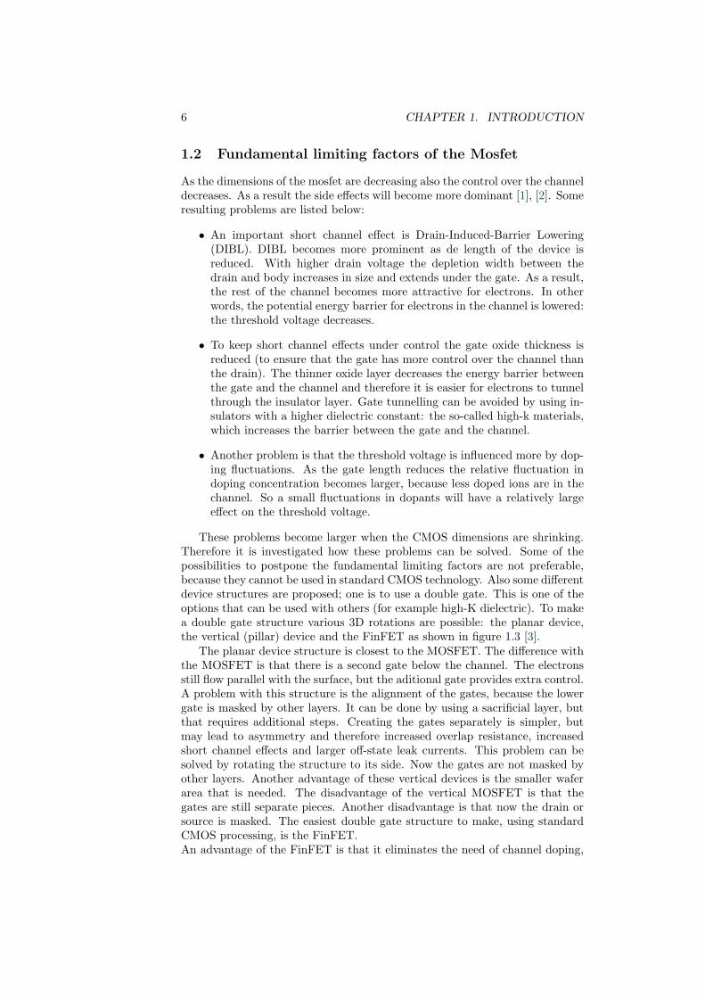
These problems become larger when the CMOS dimensions are shrinking.Therefore it is investigated how these problems can be solved. Some of thepossibilities to postpone the fundamental limiting factors are not preferable,because they cannot be used in standard CMOS technology. Also some differentdevice structures are proposed; one is to use a double gate. This is one of theoptions that can be used with others (for example high-K dielectric). To makea double gate structure various 3D rotations are possible: the planar device,the vertical (pillar) device and the FinFET as shown in figure 1.3 [3].
The planar device structure is closest to the MOSFET. The difference withthe MOSFET is that there is a second gate below the channel. The electronsstill flow parallel with the surface, but the aditional gate provides extra control.A problem with this structure is the alignment of the gates, because the lowergate is masked by other layers. It can be done by using a sacrificial layer, butthat requires additional steps. Creating the gates separately is simpler, butmay lead to asymmetry and therefore increased overlap resistance, increasedshort channel effects and larger off-state leak currents. This problem can besolved by rotating the structure to its side. Now the gates are not masked byother layers. Another advantage of these vertical devices is the smaller waferarea that is needed. The disadvantage of the vertical MOSFET is that thegates are still separate pieces. Another disadvantage is that now the drain orsource is masked. The easiest double gate structure to make, using standardCMOS processing, is the FinFET.An advantage of the FinFET is that it eliminates the need of channel doping,

1.2. FUNDAMENTAL LIMITING FACTORS OF THE MOSFET 7
Figure 1.3: Planar, vertical and FinFET architectures
thereby reducing parametric spread due to dopant fluctuations and reducingjunction leakage due to high electric fields. The reduction of leakage currentsenables a steeper subthreshold slope and therefore lowers the power consump-tion (mainly of digital circuits). Besides the reduction of the leakage currentsthe multigate topology of the FinFET also increases the current of the devicewith a factor two. A disadvantage of the smaller dimensions of the fin and theundoped channel is the increasing source/drain resistance.
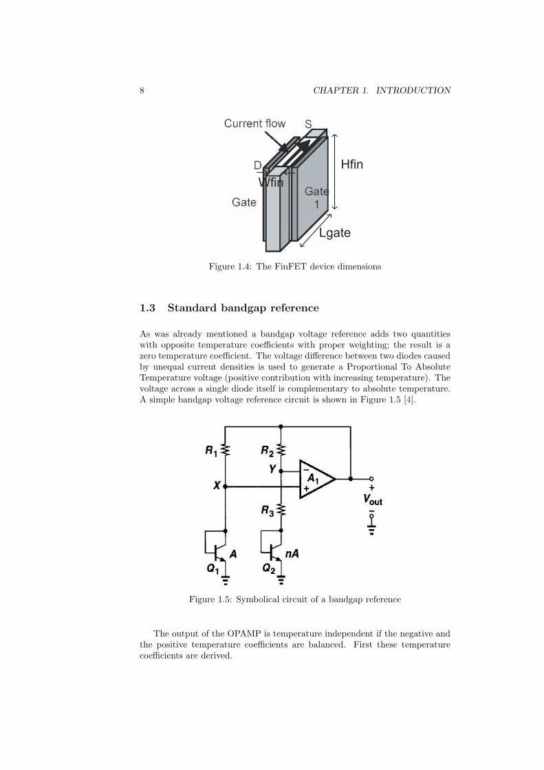
The crucial geometric device dimensions for the FinFET are (shown in fig-ure 1.4):Lgate = Gate length, the length of the gate metal.Wfin = Width of the fin, the distance between the gate oxides of the two gates.Hfin = Height of the fin, the distance between the buried oxide and the topgate oxide.
8 CHAPTER 1. INTRODUCTION
Hfin
Lgate
Wfin
Figure 1.4: The FinFET device dimensions
1.3 Standard bandgap reference
As was already mentioned a bandgap voltage reference adds two quantitieswith opposite temperature coefficients with proper weighting; the result is azero temperature coefficient. The voltage difference between two diodes causedby unequal current densities is used to generate a Proportional To AbsoluteTemperature voltage (positive contribution with increasing temperature). Thevoltage across a single diode itself is complementary to absolute temperature.A simple bandgap voltage reference circuit is shown in Figure 1.5 [4].
Figure 1.5: Symbolical circuit of a bandgap reference
The output of the OPAMP is temperature independent if the negative andthe positive temperature coefficients are balanced. First these temperaturecoefficients are derived.

1.3. STANDARD BANDGAP REFERENCE 9
1.3.1 Negative temperature coefficient
The forward (base emitter) voltage of a pn-junction diode exhibits a negativetemperature coefficient. To get an expression for this temperature coefficientthe equation for the diode current is rewritten.
IC = IC,0Tηe
(q(Vbe−Vgap,0)
KbT ) (1.1)
IC = Is expqVbeKbT
Vbe =KbT
qln( IC(T )IC,0T η
)+ Vgap,0
with:IC,0 a process and size-dependent constant;
Is = IC,0Tηe
(q(−Vgap,0)
KbT )
η ≈ 4 a mobility-related constant;T the temperature in K;Vgap,0 the bandgap extrapolated to T=0K.
To find the temperature coefficient the derivative of the Vbe to temperature hasto be taken (for this q
KbTis rewritten as VT ).
∂Vbe,VT
∂T=∂VT∂T
ln(IcIs
)− VtIs
∂Is∂T
(1.2)
with:∂Is∂T
= µ0Kb(η)T η−1e(−VgkT ) − µ0KbT
η(−VgKbT 2
)e(−VgKbT ) (1.3)
andVtIs
=VT
µ0kT ηe(−VgKbT )
(1.4)
Substituting these in in equation 1.2 gives:
∂Vbe,VT
∂T=
∂VT∂T
ln(IcIs
)− ηVT
T+ VT
( VgKbT
)(1.5)
=Vbe − ηVT − Vg
q
T
1.3.2 Positive temperature coefficient
The voltage with a positive temperature coefficient is typically derived froma voltage difference between two diodes caused by unequal current densities.These unequal current densities can be forced in two ways; the current throughthe equal diodes can be different, or the diode area of the two diodes can bedifferent. This is schematically shown in figure 1.6.
10 CHAPTER 1. INTRODUCTION
Figure 1.6: Simplified bandgap reference
The diode voltage difference is:
∆Vdiode = Vbe1 − Vbe2 (1.6)
= VT ln(nI0Is1
)− VT ln(I0AIs2
)
= VT ln(nI0 − Is1
)− ln
(I0 −AIs2
)
= VT ln(AnIs2
Is1
)with n the current density ratio and A the diode area ratio.
To find the temperature coefficient the derivative of the Vbe to temperature hasto be taken.
∂Vbe∂T
=Kb
qln(nA) (1.7)
1.3.3 Reference voltage
When the temperature coefficients are known, an equation can be derived forthe reference voltage (for the standard bandgap topology using resistors, seefigure 1.1):
Vout = I(R2 +R3) +KbT
qln( IC(T )IC,0T η
)+ Vgap,0 (1.8)
= I(R2 +R3) + Vdiode2
The diode current is:
I =KbTq ln(An)
R3(1.9)
This gives for the output voltage:
Vout =KbT
qln(An)
(R2 +R3)R3
+ Vdiode2 (1.10)
In equation (1.10) the first term is PTAT, while the second is CTAT. To makethe reference voltage temperature independent the weighting should be chosenproperly:
∂Vdiode∂T
R2 +R3
R3= −∂VV t
∂T(1.11)

1.3. STANDARD BANDGAP REFERENCE 11
Substituting equation 1.7 and equation 1.5 yields:
R2
R3= −
Vdiode−ηVT−Vgq +
Kbq ln(An)
TKb
q ln(An)(1.12)
This simple bandgap reference cannot be implemented in FinFET technol-ogy because of two reasons. Firstly for its implementation three resistors areneeded. For low power operation these need to be high ohmic. In FinFETtechnology these are difficult to make, because only metal(lic) gates are avail-able to make resistors. This means no area efficient high-ohmic resistors canbe made.Secondly the reference voltage is higher than the supply voltage.It can be concluded that a low-voltage bandgap reference topology needs to befound. In literature, low-voltage references can be found. Some are discussedin the next section.

12 CHAPTER 1. INTRODUCTION
1.4 Bandgap reference topologies / Solution proposal
Standard bandgap reference topologies need a supply voltage that is higherthan the 1V supply that is available in the FinFET process. To be able to op-erate bandgap references at a supply voltage lower than the material bandgap,the bandgap reference circuits must have an output voltage lower than the sil-icon material bandgap voltage.
Associated with implementation in SOI FinFET technology include the useof high ohmic resistors and diodes; these cannot be made accurately in a SOIFinFET process.
In the next sections some architectures that use low supply voltages andalso some circuits that do not require high-accuracy resistors are explored. Alow voltage bandgap reference topology is chosen in section 1.5; which alsogives the outline of the thesis.

1.4. BANDGAP REFERENCE TOPOLOGIES / SOLUTION PROPOSAL13
1.4.1 Current domain bandgap reference
The bandgap reference topology proposed by Banba [5] is one of the mostwidely applied approaches to create good sub-1V bandgap reference circuits.A disadvantage of this approach is that it uses a number of matched high-ohmic resistors that take a significant die area for low power reference circuits.In FinFET technology this is even a larger problem because only metal(lic)gates can be used to make resistors.
The principle of Banba is that instead of voltages, currents are added. Thisis done by using the additional resistors. A PTAT current (I2a) and a CTATcurrent (I2b and I1b) are added. This gives a current that is independent oftemperature (I2). The circuit is shown in figure 1.7.
Figure 1.7: resistor subdivision bandgap reference
In the bandgap reference of Banba the two extra resistors are equal:
R1 = R2 (1.13)
Due to the feedback loop around the OPAMP the voltages Va and Vb are thesame.
Va = Vb (1.14)
Also the transistors p1, p2 and p3 are the same:
I1 = I2 = I3 (1.15)
The PTAT current I2a is known:
I2a = IPTAT =dVfR3
(1.16)
with the voltage difference over the diode:
dVf = Vf1 − Vf2 =KbT
qln(N) (1.17)
Also the CTAT current is known:
I2b = ICTAT =VaR2
(1.18)
It follows that the current I2 consists of I2a (PTAT current) and I2b (aCTAT current). By choosing the resistors correctly, a temperature independent

14 CHAPTER 1. INTRODUCTION
current can be generated. This current is then copied to the third branch whichgenerates a reference voltage:
Vref = R4
( VaR2
+dVfR3
)(1.19)
The disadvantage of this circuit is the use of additional high ohmic resis-tors. These can be made in FinFET technology, but only metal(lic) gates areavailable to make resistors. This means no area efficient high ohmic resistorscan be made.
What is interesting in this bandgap reference circuit is the idea to mirror acurrent (the added PTAT current and CTAT current) to an extra resistor togenerate the reference voltage.

1.4. BANDGAP REFERENCE TOPOLOGIES / SOLUTION PROPOSAL15
1.4.2 Multi stage bandgap reference
One idea to eliminate the most high-ohmic resistor is found in the solution ofAnnema [7].In conventional bandgap references (shown in figure 1.8), a PTAT voltage acrossa resistor compensates the negative temperature dependency of the voltage ona diode. For low power consumption, the current through the diodes must besmall. This means that the resistors will be quite large. Note that the upperresistor is substantially larger than the lower (N ≈ 10). Since these resistorsneed to be matched, the upper resistor will be physically large as well. If thisresistor can be removed the occupied area will be substantially smaller.
Figure 1.8: Typical CMOS bandgap reference
Elimination of the upper resistor can be done by replacing this resistor bycascaded voltage followers, with build in PTAT offset voltages. The negativetemperature coefficient of the voltage on the diode is then compensated by thisoffset voltage (the circuit is shown in figure 1.9). The leftmost part of thisbandgap reference is similar to the conventional bandgap circuit. The onlyfunction of this block is to bias the diodes.
Figure 1.9: Principle of multistage bandgap reference
The cascaded voltage follower creates a PTAT voltage offset between theinput and the output. An implementation of the voltage follower is shown infigure 1.10. In this circuit an intentional ”size mismatch” in the differential pairand/or in the current mirror can be used to make unequal current densities intwo subthreshold Mosts.
For this the differential pair needs to have an exponential behavior:
I = I0eqV
KbT (1.20)

16 CHAPTER 1. INTRODUCTION
In CMOS this can be done using DTMOST’s as these have a diode like expo-nential transfer. For one cascaded voltage follower the output voltage is:
Vout = Vin +KbT
qln( L1
W1
W2
L2
1M
)(1.21)
With M the gain off the current mirror. When using this the reference voltagewill be around 1.2V, as will a normal bandgap reference.
Figure 1.10: Schematic of the PTAT cascaded voltage follower circuit
The advantage of this topology is the reduced influence of the opamp errorto the reference voltage. In the standard bandgap this opamp error is amplifiedby the resistor factor (R2
R3in figure 1.5).
The advantage of this circuit is the reduction of the resistor dimensions.In CMOS DTMOST’s are used to generate a PTAT voltage. In FinFET tech-nology the sub-threshold behavior of a transistor has an exponential characterand therefore this topology can work in FinFET technology as well. Anotheradvantage is the reduced opamp error.
A disadvantage of the multistage bandgap reference is the high referencevoltage, which is still 1,23V: this is above the supply voltage of FinFET tech-nology.

1.4. BANDGAP REFERENCE TOPOLOGIES / SOLUTION PROPOSAL17
1.4.3 Averaging bandgap reference
Another approach is to use weighted averaging. Instead of summing a PTATand a CTAT voltage, they are averaged. Yielding a temperature independentvoltage of 0.6V [6]. The averaging bandgap is shown in figure 1.11.
Figure 1.11: The sub-1-V bandgap circuit in 32 nm FinFET technology
The voltages Vdiode and VCTAT are the same because of the feedback looparound the opamp.
Vdiode = VCTAT (1.22)
Because of this also the currents in transistors p1, p2 and p3 are the same (thecurrent mirror gain is one).
I1 = I2 = I3 (1.23)
The VCTAT is derived by the voltage over a diode.
Vdiode =KbT
qln( IcIc,0Tn
)+ Vgap,0 (1.24)
The positive temperature coefficient is the difference between the diode voltagesof the two diodes operating at different current densities. This gives a positivetemperature coefficient of:
dVf = Vf1 − Vf2 =KbT
qln(N) (1.25)
This PTAT voltage is then converted to a current with a resistor (R1). ThisPTAT current is then copied to the third branch.
The averaging of the PTAT and CTAT signal is done using matched OTAs(operational transimpedance amplifier). These are used in such a way thatOTA non-linearity is canceled.
The reference voltage is expressed by the following equation:
Vref =gmleft
gmleft + gmrightVctat +
gmright
gmleft + gmrightVptat (1.26)

18 CHAPTER 1. INTRODUCTION
When two identical OTAs are used gmleft and gmright are equal and hencethe output voltage is about 0.6V.
The advantage of this bandgap reference circuit is that it is similar to thetraditional bandgap reference and contains just two resistors, which do notneed to be so high ohmic. This is also the disadvantage of this circuit, becausethes two resistors need to be matched. Another advantage is that this circuitcan operate at a low supply voltage.

1.5. THESIS OUTLINE 19
1.5 Thesis outline
The principle of the averaging bandgap reference is used as the main principlefor the bandgap reference in this project, which can be simplified into a simpleblock diagram as shown in figure 1.12.
M1 M2
D1 D2
R1
R3 R4
1 : N
+
-Va
Vb
Vref
Vptat
Vc
Averaging
Chapter 5
CTAT
Chapter 4
PTAT
Chapter 3
Chapter 6
Figure 1.12: The averaging bandgap reference topology with chapter index
For all sub-blocks it is important that no high precision resistors and nohigh ohmic are used. Some other relevant target properties of the bandgapreference circuit that have to be taken into account are listed below:Vref ≈ 0.6Vσvref = 0.5%PSRR (Power Supply Rejection Ratio) = 40dB.
The PTAT voltage is made by cascaded voltage followers, with build-inPTAT offsets (see section 1.4.3); the design of this PTAT stage is shown inchapter 2.The CTAT sub-block uses a triode resistor for R1. To make this triode resistoraccurate over larger voltage swings both, a N-type and a P-type FinFET areused. These triode resistor need to be biased with a voltage that is independentof the supply voltage (see chapter ??).The averaging of the CTAT and the PTAT voltage is done using two stages oftransimpedance amplifiers (see chapter 4).
The simulation results of the complete bandgap reference as well as thelayout are presented in Chapter 5.
Finally in the conclusion the results of all chapters are summarized, andrecommendations for future research are listed.


Chapter 2
PTAT voltage generator
In an averaging bandgap reference circuit in SOI FinFET technology resistorshave to be eliminated, because these are not easily realized in SOI FinFETtechnology (metal gates). Therefore, it is not possible to have resistor-basedamplification of the PTAT signal. A solution for the PTAT side may be foundin summing a number of small PTAT voltages instead of amplifying it to therequired level. In this case the PTAT voltage can be completely independentof the rest of the circuitry.
2.1 Insensitivity to resistance variation
In conventional topologies, the PTAT voltage is generated on the CTAT sideand then amplified. The resistor in the PTAT circuit can be replaced by sepa-rate PTAT voltage reference. It needs to be investigated what the error on thereference voltage due to mismatch will be. Both the conventional solution andthe solution that uses a separate PTAT voltage reference are examined. Theschematics of an averaging bandgap reference and of the circuit with resistorR2 replaced by a (PTAT) voltage source are shown in figure 2.1
M1 M2 M3
D1 D2
R1 R2
R3 R4
1 : N
+
-Va
Vb Vc
Vref
M1 M2
D1 D2
R1
R3 R4
1 : N
+
-Va
Vb
Vref
Vptat
Vc
A) B)
+
Figure 2.1: The schematic of an averaging bandgap reference: a) the con-ventional averaging bandgap reference circuit and b) the averaging bandgapcircuit, with R2 replaced by a (PTAT) voltage source
21

22 CHAPTER 2. PTAT VOLTAGE GENERATOR
On-chip resistors substantially spread batch-to-batch and variate over temper-ature. Resistance variation gives an error in the current through the diodes.
Iptat =KbTq ln(n)
R1(2.1)
∆Iptat =KbT
qln(n)
∆R1
R21
The total error on the reference voltage consists of the PTAT voltage error andthe CTAT voltage error.
∆Vref =12
(∆Vctat + ∆Vptat) (2.2)
This equation is used in the next sections to calculate the batch-to-batch vari-ation and the temperature variation.

2.1. INSENSITIVITY TO RESISTANCE VARIATION 23
2.1.1 Batch-to-batch variation
First the effect of batch-to-batch variation of the traditional averaging bandgapreference is examined. The influence of current error on the PTAT voltage isgiven by:
∂Vptat∂Iptat
= R2 (2.3)
The PTAT voltage changes due to a deviation in resistors R1 and R2:
∆Vptat = −KbT
qln(nA)
∆R1
R21
R2 +KbT
qln(nA)
∆R2
R1(2.4)
When the resistors are matched it is seen that both contributions are equal.
∆R1
R1=
∆R2
R2→ ∆R2
R1=
∆R1
R21
R2 (2.5)
For the CTAT voltage error the following equation is derived:
∆Vctat =∂KbT
q ln( Ic
Ic0) + Vgap
∂I∆I (2.6)
=KbT
q
∆IIc
The total error due to batch-to-batch variation is:
∆Vref =12
(KbT
q
∆IIc
)(2.7)
For the averaging bandgap reference with the PTAT source the same can bedone. The influence of a current error on the PTAT voltage then is:
∂Vptat∂Iptat
= 0 (2.8)
In the PTAT voltage source implementation, the PTAT voltage is not influ-enced by the current variation at all, because the current is not used on thePTAT side of the circuit. It is thus seen that batch-to-batch resistance varia-tion has no influence on the PTAT voltage for both circuits.The CTAT circuit of this bandgap reference is the same as in the traditionalaveraging bandgap reference circuit and therefore, also in the CTAT circuit thevariation is the same.

24 CHAPTER 2. PTAT VOLTAGE GENERATOR
2.1.2 Temperature variation
The negative temperature coefficient error due to variation in R1 is:
∆VCTAT =∂VCTAT,error
∂R1
∂R1
∂T∆T (2.9)
With an approximation of the resistor including linear temperature dependen-cies:
R = R0 + α(T − T0) (2.10)
the temperature variation of the CTAT voltage is (derivation in appendix A.1):
∆VCTAT =∂VCTAT,error
∂R1
∂R1
∂T∆T = −KbT0
qα∆T (2.11)
It is seen that the temperature dependence of the resistor influences the nega-tive temperature coefficient. This change is linear with temperature and there-fore in the design of the negative temperature coefficient it can be compensated.Note that this only holds when the temperature dependence of the resistor is(more or less) linear.In the standard averaging bandgap reference circuit this is different, becausethere the resistors are matched and therefore the temperature variation in theresistors are canceled.
With the effects of batch-to-batch variation and temperature variation ofresistors known, it can be concluded that in theory it is possible to replace oneresistor by a PTAT voltage reference. What has to be taken into account isthat the temperature coefficient of the CTAT voltage and the absolute CTATvoltage slightly changes.

2.2. CASCADED PTAT VOLTAGES 25
2.2 Cascaded PTAT voltages
The PTAT voltage is generated by cascading a number of voltage followerswith a build in offset voltage [7], see figure 2.2.The cascaded voltage follower creates a PTAT voltage offset between the in-put and the output. This offset can be made by using an intentional ”sizemismatch” in the differential pair and/or a non-unity mirror gain to make anoffset voltage. For this offset voltage to be PTAT the differential pair needs tohave an exponential behavior. One stage gives an output voltage of:
I = I0W
Le
qVKbT (2.12)
Vout = Vin +KbT
qln(NK
)
PTATPTAT
PTAT
+
++
--
-Vc
gnd
Figure 2.2: The cascading of the voltage followers
were N is the ”size mismatch” in the differential pair and K the gain of thecurrent mirror.
A possible implemention of the voltage follower is shown in figure 2.3.
+
-
1K
Vin
Vout
I
M0
M3
M1
M2
Vin Vout
Vs
Vp
Vx
>120mV>120mV
212mV
<300mV
1 : N
Figure 2.3: The PTAT voltage circuit with in blue the low temperature voltagesand in red the high temperature volatges
Now some conditions for the voltage follower are given.

26 CHAPTER 2. PTAT VOLTAGE GENERATOR
• The positive temperature coefficient needs to be equal to the negativetemperature coefficient.
MKb
qln(NK) =
∂VCTAT∂T
(2.13)
=Vbe − 2.5KbT
q − EgT
NK = e
∂VCT AT∂T
Kbq
M
In this equation M is the number of voltage follower stages and N isL1W1
W2L2
. W1, L1, W2 and L2 are the dimensions of the differential pairtransistors.
• The differential pair needs to operate in subthreshold; therefore the gatesource voltage of these transistors needs to be lower then the thresholdvoltage.
Vgs,diff < Vthp (2.14)
• All transistors need to be in saturation: the drain source voltage of eachtransistor must be larger than approximately 3KTq . This means that theoutput voltage swing is limited; the drain source voltage of the currentmirror needs to be larger then Vds,sat. Also the drain source voltage ofthe differential pair needs to be larger the Vds,sat. Therefore the outputvoltage of a single stage, given in figure 2.3, must satisfy:
Vx − Vds,sat > Vout >3KbT
q(2.15)
The proposed schematic of figure 2.3 has voltage headroom problems. Whenthe the PTAT cascaded voltage followers are connected in stead of the resistor(see figure 2.1b ), the input of the first stage will be ground. At low tem-peratures (−400C) , the drain-source voltage of the current mirror needs tobe larger than approximately 120mV , to be in strong inversion (if the volt-age is lower, the transfer of the current mirror has a large error). The drainof the current mirror is connected directly to the output, at low temperaturethe output voltage is therefore ≥ 120mV . From this the minimum positivetemperature coefficient can be calculated: 120mV/233K = 0.51mV/K. Athigh temperature (1400C) the output voltage will then minimally be 212mV .At this temperature, the voltage node Vx must be smaller than the thresholdvoltage (300mV ) (only for the first stage, because the input is ground). Thismeans that the drain-source voltage of the right transistor of the differentialpair will be smaller than 100mV : it operates in triode (all voltages are shownin figure 2.3).
Also, since the input voltage is 0V , the voltage on node Vx will be no higherthan the threshold voltage. For the drain-source voltage of the input transistorto be high enough (so that it is not in triode) the current mirror transistor needsto be biased in the deep sub-threshold region. This is highly undesired because
2.2. CASCADED PTAT VOLTAGES 27
it requires very large transistors for matching. Furthermore, any voltage errorbetween the transistors will lead to a significant error in the transfer.Concluding, it can be stated that there is insufficient voltage headroom at theinput side of the PTAT voltage source if the input of the first PTAT stage isground.
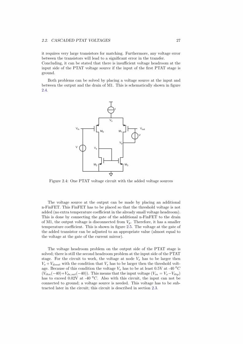
Both problems can be solved by placing a voltage source at the input andbetween the output and the drain of M1. This is schematically shown in figure2.4.
I
V
V
M0
M3
M1
M2
Vin Vout
Vs
Vp
Vx
Figure 2.4: One PTAT voltage circuit with the added voltage sources
The voltage source at the output can be made by placing an additionaln-FinFET. This FinFET has to be placed so that the threshold voltage is notadded (no extra temperature coefficient in the already small voltage headroom).This is done by connecting the gate of the additional n-FinFET to the drainof M1, the output voltage is disconnected from Vp. Therefore, it has a smallertemperature coefficient. This is shown in figure 2.5. The voltage at the gate ofthe added transistor can be adjusted to an appropriate value (almost equal tothe voltage at the gate of the current mirror).
The voltage headroom problem on the output side of the PTAT stage issolved; there is still the second headroom problem at the input side of the PTATstage. For the circuit to work, the voltage at node Vx has to be larger thenVs +Vdssat with the condition that Vs has to be larger then the threshold volt-age. Because of this condition the voltage Vx has to be at least 0.5V at -40 0C(Vthn(−40)+Vds,sat(−40)). This means that the input voltage (Vin = Vx−Vthp)has to exceed 0.02V at -40 0C. Also with this circuit, the input can not beconnected to ground; a voltage source is needed. This voltage has to be sub-tracted later in the circuit; this circuit is described in section 2.3.
28 CHAPTER 2. PTAT VOLTAGE GENERATOR
I
V
M0
M3
M1
M2
Vin Vout
M4
I
Vs
Vp
Vx
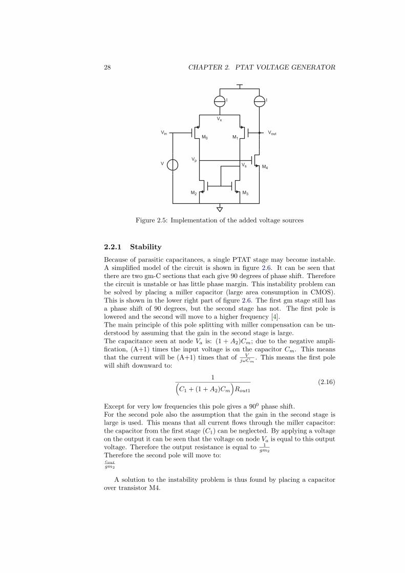
Figure 2.5: Implementation of the added voltage sources
2.2.1 Stability
Because of parasitic capacitances, a single PTAT stage may become instable.A simplified model of the circuit is shown in figure 2.6. It can be seen thatthere are two gm-C sections that each give 90 degrees of phase shift. Thereforethe circuit is unstable or has little phase margin. This instability problem canbe solved by placing a miller capacitor (large area consumption in CMOS).This is shown in the lower right part of figure 2.6. The first gm stage still hasa phase shift of 90 degrees, but the second stage has not. The first pole islowered and the second will move to a higher frequency [4].The main principle of this pole splitting with miller compensation can be un-derstood by assuming that the gain in the second stage is large.The capacitance seen at node Va is: (1 + A2)Cm; due to the negative ampli-fication, (A+1) times the input voltage is on the capacitor Cm. This meansthat the current will be (A+1) times that of V
jωCm. This means the first pole
will shift downward to:
1(C1 + (1 +A2)Cm
)Rout1
(2.16)
Except for very low frequencies this pole gives a 900 phase shift.For the second pole also the assumption that the gain in the second stage islarge is used. This means that all current flows through the miller capacitor:the capacitor from the first stage (C1) can be neglected. By applying a voltageon the output it can be seen that the voltage on node Va is equal to this outputvoltage. Therefore the output resistance is equal to 1
gm2Therefore the second pole will move to:cout
gm2
A solution to the instability problem is thus found by placing a capacitorover transistor M4.

2.2. CASCADED PTAT VOLTAGES 29
I
VS
M0
M3
M1
M2
Vin
gm1
M4
I
C1 C2
Vin
Vout
Cm
gm1 gm2
Vx
Va
Cm
C1 C2
Vin
Voutgm1 gmgm2
Va
+ +
- -
+ -gm2
C1 C2
Va
Figure 2.6: The instable ptat voltage source. The upper shows the ptat voltagesource circuit; lower left: an equivalent model lower right: solution with themiller feedback capacitor
For this solution of the PTAT circuit, however, an other instability problemwas found. The circuit is susceptible to (relaxation) oscillations due to channelcharge re-location. For normal operation an equation for the output voltagecan be derived from the small signal equivalent circuit (see appendix A.3):
vout = −vigm0gm1
gm0 + gm1
(k + 1)jωC
(2.17)
It can be seen that for normal operation the PTAT voltage source is stable(a rising input voltage causes the output voltage to decrease). On the otherhand when charge relocation is taken into account the voltage source becomesinstable.When the output voltage becomes lower, the gate-source voltage of M1 willreach the threshold voltage. At this point in time the channel charge is accu-mulated and a positive current is flowing into the device. This effect can bemodeled as a current source with the sign opposite to the ordinary small signalequivalent. (when the voltage on the gate decreases the current flowing fromthe discharging of the channel increases). So when the channel dischargingeffect becomes larger then the normal current the effective gm changes sign.Therefore the output voltage equation changes to:
vout = vigm0gm1
gm0 + gm1
(k + 1)jωC
(2.18)
This behavior results in a positive feedback mechanism: it behaves as a re-laxation oscillator. A solution to this problem is found by making two paths

30 CHAPTER 2. PTAT VOLTAGE GENERATOR
from the sub-threshold FinFET to the output. This is done with additionalcurrent mirrors which copy the currents of the differential pair directly to theoutput. Therefore the PTAT stage contains just one (effective) gm stage witha capacitive load. All intermediate stages in the circuit have no gain and havetheir poles at a high frequency. This means that there is little phase-shift inthe intermediate stages and the total gain of the circuit is lower (more stable).The final PTAT voltage circuit is shown in figure 5.17.
I
M0
M3
M1
M2
Vin Vout
C
M5
M4 M7
M6
Vx
Vin
Vout
=
Figure 2.7: The final design of the PTAT voltage circuit
In this circuit the ”size mismatch” of the differential pair is realized bychoosing the width of M1 N times larger than M0 and the non-unity mirrorgain will be made by choosing the width of M3 k times M2.

2.3. ADD AND SUBTRACT CIRCUIT 31
2.3 Add and subtract circuit
The input of the first stage of the PTAT voltage source cannot be connected toground. Therefore a voltage has to be added and later in the circuit subtracted.The input voltage must have the following limitations:
0.08V < Vadd < 0.4V (2.19)
The lower limit is the voltage that is needed to have enough voltage headroomin the input branch of the PTAT voltage circuit. The higher limit comes fromthe voltage at node Vx; this needs to be lower then approximately 0.9V to haveenough voltage room for the current source. Therefore it has to be investi-gated what the temperature coefficient of the added voltage can be and afterhow many stages the voltages is subtracted. Another important issue is thatthe added and the subtracted value have to be equal (a small difference willintroduce an error in the reference voltage).
The voltage at the input of the first PTAT voltage stage can either have apositive or a negative temperature coefficient or it can be temperature indepen-dent. It is undesirable to have a positive temperature coefficient voltage sourcereferenced to the supply voltage, because then the circuit will be dependenton the supply. Referring it to ground is difficult, because this voltage can noteasily be connected to the gate (source voltage constant) of a n-FinFET (thenthe current will increase too much for high temperatures). When a negativetemperature dependent voltage source is added, the output voltage of the sec-ond stage will be too high at low temperature. The added voltage must thenbe subtracted after the first stage. When this is done the input voltage of thesecond stage will be too low at low temperatures.
A solution to this problem is to use a temperature independent voltagesource. A temperate independent voltage can be made by using the reference(output) voltage. Connecting the reference voltage directly to the input is notpossible, this voltage is too high (0.08V < Vadd < 0.4V ); the voltage at nodeVx needs to be lower then approximately 0.9V. Therefore the reference voltageis divided by two.By using part of the reference voltage to bias the PTAT circuit a feedback loopis made. Therefore it has to be checked whether the circuit will start up. Thelower limit of the PTAT voltage is 0.08V; the worst case reference voltage hasto be higher then his voltage. The worst case is when the PTAT output voltageis still zero and the CTAT voltage will be (at low temperature) 0.37V; the ref-erence voltage is then half of this (Vref = 0.5(VPTAT +VCTAT )) and the inputto the PTAT voltage is half the reference voltage(Vin,PTAT = 0.5Vref = 0.09V .This means that the reference voltage will be higher than the required inputvoltage of the PTAT; the PTAT will start-up. The reference voltage can thusbe used as an input voltage of the PTAT circuit.
Next the subtract circuit has to be placed. Therefore the number of PTATstages need to be known. A PTAT circuit with only one stage is not possible,because a voltage has to be added to the input; the output voltage will then beabove the supply voltage. A PTAT voltage with two stages is also not possible;when the input voltage is subtracted after the first stage this voltage is too low

32 CHAPTER 2. PTAT VOLTAGE GENERATOR
(at low temperatures) for the subtract circuit.A PTAT voltage circuit with three and four stages are feasible to make. Morethan five stages is not usefull; it only increases power consumption and devicesizes (mismatch).The choice is made to make a PTAT voltage circuit with four stages, whenmore stages are used the demands on noise and offset for the individual blocksincrease. This is because in this multistage approach, noise and offset con-tributions of individual circuits are summed; the total noise and offset at theoutput of N cascaded blocks equals
√N times the noise and offset of a single
circuit.
The implementation of the add subtract circuit is shown in figure 2.8. Thevoltage divider is implemented (of the reference voltage) by cascoding two equalFinFETs (M4 and M5). These transistors are designed in such a way that theycarry a certain current that is within reasonable bounds over temperature.This current is then copied with M3 to the second branch. If all transistors arechosen equal (Vgs,5 = Vgs,4 = Vgs,3 = Vgs,2 = 1/2Vref ) the currents throughboth branches is the same. This way, the gate of M2 has a voltage of 1
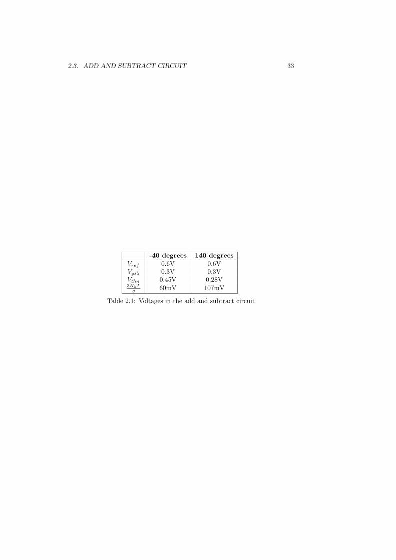
2Vref +VPTAT . At the source of M2 the voltage is the PTAT voltage. The voltages inthe add subtract circuit are shown in table 2.1.
M5
M4
M2
M3
ptat
Vref
Vref + Vptat
Vptat
Id Id
12 Vref
12
Figure 2.8: Division by two of the reference voltage
Due to the large threshold variation over temperature, all FinFETs will bein subthreshold at low temperature and in strong inversion at high temperature(see table below). For M3, this gives the condition that when the FinFET isin strong inversion, the drain voltage should exceed 3KbT
q . Therefore the inputvoltage can only be subtracted when this condition is met.
2.3. ADD AND SUBTRACT CIRCUIT 33
-40 degrees 140 degreesVref 0.6V 0.6VVgs5 0.3V 0.3VVthn 0.45V 0.28V3KbTq 60mV 107mV
Table 2.1: Voltages in the add and subtract circuit

34 CHAPTER 2. PTAT VOLTAGE GENERATOR
2.4 Design of a single stage
In the previous sections some design criteria of a single PTAT section and theadd/subtract circuit are derived. Attention can now be paid to optimize thedesign of one PTAT stage. The circuit is optimized to low power consumptionand a small area. This can be done using noise calculations and mismatchcalculations.
2.4.1 Mismatch
Device mismatch can be modeled by a threshold voltage mismatch. This isshown in equation 2.20:
σV th =AV th√WL
(2.20)
The mismatch (referred to the output) of the differential pair (σV th,out,d) andthe current mirror (σV th,out,c) is:
σV th,out2 = σV th,out,c
2 + σV th,out,d2 (2.21)
The output voltage mismatch due to device mismatch in the differentialpair is:
σV th,out,d =
√( AV th√W0L0
)2
+( AV th√
W1L1
)2
(2.22)
Note that the current density in M0 must be N times larger then in M1. This isdone by taking W1
√N times W0 and L0
√N times L1. This way the current
density ratio is n, but both devices have an equal contribution to the mismatch(equal areas). The total output voltage mismatch due to device mismatch inthe differential pair is then:
σV th,out,d =√
2( AV th√
W0L0
)2
(2.23)
Using a small signal equivalent circuit, the output referred voltage due todevice mismatch in the current mirror is calculated. This is shown for M3 infigure 2.9.
From the figure an expression for the mismatch on one side of the currentmirror is given:
σV th,out,c = −gm0 + gm1
gm0gm1
gm3gm2
gm2 + gm3σV th (2.24)
For the other side the mismatch transfer is the same. Note that the currentratio in the branches differs, there is a device ratio in the current mirror (k).

2.4. DESIGN OF A SINGLE STAGE 35
Figure 2.9: Small signal circuit of the effect of mismatch on one side of thecurrent mirror
Therefore, the total expression of the (referred to output) mismatch of thecurrent mirror is:
σV th,out,c =
√(1k
+ 1)gm0 + gm1
gm0gm1
gm3gm2
gm2 + gm3σV th (2.25)
Note that gm2 =√kgm3 and gm0 = kgm1 (subthreshold). Rewriting this (see
appendix A.4.1) so that is can be expressed with area gives:
σV th,out,c =
√(k + 1k
)1 + k
1 +√k
1√k
√2
40AV th
Vgt√W3L3
(2.26)
Summing individual contributions:
σV th,out2 = σV th,out,c
2 + σV th,out,d2 (2.27)
= (k + 1k
)(1 + k)2
(1 +√k)2
1k
2402
AV th2
V 2gtW3L3
+√
2AV th
2
W0L0
Since there are M PTAT stages cascaded, the total variance of the PTAT volt-age is M times the mismatch error shown in equation 2.27. It can be seenthat when the number of sections (M) is smaller the σV th,out per section canbe higher and still have the same total mismatch. This means that the size ofthe FinFETs can be chosen smaller (taking into account that the width andlength proportion as well as the minimum possible width and length have tobe taken into account). So for the area it is better to take less sections (takinginto account that you still have to make Mln(nk) = 0.6V .Rewriting equation 2.27 gives the total required (active) area of one PTAT volt-age stage as a function of k (the device ratio in the current mirror). Optimizingfor k and n yields:
Atot =√
2AV th2(σV th,out2 − (k+1
k ) k2+2k+1k+2√k+1
1k
2402V 2
gt
AV th2
A3
) +A3 (2.28)
The required area should be minimized; the derivation is found in appendixA.4.1.
The following optimum is found:k = 1.803442406

36 CHAPTER 2. PTAT VOLTAGE GENERATOR
N = 112.5625079
For a given output voltage mismatch, the required size (area) of all tran-sistors is known. The aspect ratio of the transistors (W/L) is determined bynoise calculations. Figure 2.10 shows the required area as a function of thetolerated mismatch. It is seen that when a larger sigma is allowed then thetotal area will decrease drastically.
For the required area it has to be taken into account that in this plot the
Figure 2.10: Total required area of one section versus the output voltage mis-match of the PTAT stage
mismatch versus area of one PTAT stage is plotted.

2.4. DESIGN OF A SINGLE STAGE 37
2.4.2 Noise
The noise generated by the PTAT voltage circuit is calculated, by summingindividual noise contributions of each FinFET. The total noise in one sectionof the PTAT voltage is shown in equation 2.29 (see appendix A.5.):
V 2noise,tot = V 2
noise,m0 + V 2noise,m1 + V 2
noise,m2 + V 2noise,m3 (2.29)
=(Inoise,m0
gm0
)2
+(Inoise,m1
gm1
)2
+(Inoise,m2
kgm1
)2
+(Inoise,m3
gm1
)2
This equation holds for both the flicker noise and the thermal noise. Thermalnoise is used to optimize the PTAT circuit.
The thermal noise density of a single (long channel device) is given:
I2noise =
83KbTgm (2.30)
The total thermal noise density is:
V 2noise,tot =
83KbT
(gm0
gm20
+gm1
gm21
+gm2
k2gm21
+gm3
gm21
)(2.31)
Rewriting:
V 2noise,tot =
83KbT
140I3
( 1K
+ 1)(
1 +
√2knW3
L3
40√I3
)(2.32)
Integrating the noise density over a certain frequency range yields the effectivenoise. It is not known what the bandwidth is; it is assumed that this is 1 GHz.The standard deviation is thus expressed by the following equation:
σ2vn =
∫ 1GHz
0
V 2noise,totdf (2.33)
Rewriting (2.33) yields an expression for the minimum I3 as a function of thenoise bandwidth:
I3 = f8KT120σ2
(( 1K
+ 1)(
1 +2
40Vgt3
))(2.34)
Note that I2 = KI3.

38 CHAPTER 2. PTAT VOLTAGE GENERATOR
2.4.3 Device dimensions
Now that the currents and k and N are known, the device dimensions (aspectratios) can be calculated. Note that the differential pair is in sub-threshold andthe current mirror in saturation (for the sub-threshold slope of a p-FinFET thesimulated curves are curve fitted):
Id =W
LId010−10−at+b
eqVgsKbT (2.35)
= knW
L
(Vgs − Vth
)2
where T is the temperature in degrees Celsius. For this the sub-threshold pa-rameters a and b also need to be known; these are determined by measurements(a = 1.7510−3 and b = 1.14 see appendix A.2).

2.5. SUMMARY 39
2.5 Summary
The design criteria of this chapter are given in the schematic of the add subtractcircuit with one PTAT voltage stage shown in figure 2.11.
I
M0
M3
M1
M2
Vin Vout
C
M5
M4 M7
M6
Vx
M15
M14
Vref
Id
12 Vref
Vref
Id
12 Vref
M12
M13
Id
1 : N
1K
+
-
Vds13
Vin
Vout
Vadd Vsubtract
Figure 2.11: The schematic of a PTAT source with the add and subtract circuit(grey)
The PTAT voltage temperature coefficient is made by an intentional ”sizemismatch” in the differential pair and a non-unity mirror gain. The totaloffset voltage temperature coefficient must be equal to the negative temperaturecoefficient. Which is approximately -1.8mV/K (from measurements). For fourstages the ”size mismatch” in the differential pair and the non-unity mirrorgain (see figure 5.17) can be calculated:
MKb
qln(NK) = −NTC (2.36)
NK = e
−NT C
MKbq
The differential pair must be biassed in sub-threshold:
• Vgs,diff < Vth,p (operate in sub-threshold)

40 CHAPTER 2. PTAT VOLTAGE GENERATOR
Attention need to be paid to:
• Vgs,cm > Vth,n (operate in strong inversion)
• Vds,m0&Vds,m1&Vds,m3 > Vds,sat.
• Vds,m13 > Vds,sat.

Chapter 3
The CTAT voltage generator
In the previous chapter the PTAT voltage circuit was designed. This chapterdeals with the CTAT voltage circuit. The schematic of a conventional CTATvoltage generator is shown in figure 3.1.
M1 M2
D1 D2
R1
1 : N
+
-Va
VbVctat
Figure 3.1: The schematic of the NTAT voltage generator
The CTAT voltage can be expressed as:
Vctat =KbT
qln(
I
Ic0) + Vgap (3.1)
with
Iptat =KbTq ln(n)
R1(3.2)
The temperature coefficient is:
∂Vbe∂T
=Vbe − (4 +m)KbT
q − VgT
(3.3)
with Eg = 1.12eV and m = 1.5The target diode voltage is approximately 0.58V at 50 0C so the temperature
41

42 CHAPTER 3. THE CTAT VOLTAGE GENERATOR
coefficient is approximately -1.85mV/K.In the conventional CTAT circuit a resistor is used. In SOI FinFET technologythe use of high ohmic resistors is not possible; these cannot be made accuratelyin a SOI FinFET process. Therefore this chapter describes a CTAT voltagecircuit without resistors . This is done by replacing the resistor with a triodeFinFET. For this freplacement it is important to know the sensitivity to resis-tance variation of the CTAT voltage.It was seen (in section 2.1) that a batch-to-batch resistance variation gives achange in the current through the diodes.
∆Iptat =KbT
qln(n)
∆R1
R21
(3.4)
Taking this into account it is seen that the resistor can not vary too much(batch-to-batch and over temperature) because this will influence the CTATvoltage (the absolute value of the CTAT voltage changes with the naturallogarithmic of this current).
3.1. TRIODE FINFET RESISTANCE 43
3.1 Triode FinFET resistance
A resistance can be made by using the triode resistance of a FinFET. To usethe triode resistance two conditions have to be met:
• The sensitivity to resistance variation of the CTAT voltage has to be low
• The drain source voltage has to be much smaller then the gate overdrivevoltage
First the sensitivity to resistance variation of the CTAT voltage is exam-ined. For this both the temperature variation and the batch-to-batch variationare taken into account.
For the batch-to-batch variaton the deviation in resistance causes the cur-rent through the diode to differ and therefore also the CTAT voltage differsfrom batch-to-batch. The output voltage is then:
Vctat = Vd +KbT
qln(n) (3.5)
with:
Vd =KbT
qln( KbT
q ln(n)
Id0R
)(3.6)
The error due to batch-to-batch variation then is:
∆Vctat =∂Vctat∂R
∆R (3.7)
= −KbT
q
∆RR
It is seen that the batch-to-batch error has the same effect on the CTAT voltageas temperature variation of the resistor itself. The batch-to-batch variation ofa FinFET in triode is approximately 30%; this implies that the error voltagewill be smaller than 1mV. Therefore, the triode-resistance can be used in theCTAT circuit.
Over temperature, it is seen that the resistance variation changes the cur-rent through the diode. The resulting voltage error is shown in equation 3.8:
Verror = ∆I1
gm2(3.8)
with:
∆I =∂Id∂R
∆R (3.9)
gm2 = Idq
KbT
Id =KbTq ln(n)
R

44 CHAPTER 3. THE CTAT VOLTAGE GENERATOR
were n is the current ratio. Yields:
Verror = −KbT
q
∆RR
(3.10)
When the resistance variation over temperature and the resistance value areknown, the error voltage can be calculated.
The error due to the temperature variation is a lot larger, because also thethreshold voltage changes over temperature.
Id =KbTq ln(n)
R(3.11)
Ron,x =1
2kWL (Vgs,x − Vth)
This can be reduced by making a resistor by using the on-resistance of a n-FinFET and a p-FinFET in parallel (see figure 3.2). This results in a moreconstant resistance over a larger drain source voltage range.
M1 M2
D1 D2
1 : N
+
-Va
VbVctat
M3 M4
Vbias
+
-
Figure 3.2: The replacement of the resistor by the on-resistance of a n-FinFETand a p-FinFET in parallel
To use the on-resistance of the p-FinFET and the n-FinFET the drainsource value has to be much smaller then the gate overdrive voltage. The drainsource voltage is rather small:
Vds = VR1 =KbT
qln(n) ≈ 50mV (3.12)
The absolute value at the ctat output voltage (Vctat) is around 0.6V at roomtemperature. To have the p-FinFET in the triode region the gate voltage needto be low. This terminal can be connected to ground. The n-FinFET needsto be biased with a voltage higher then Vthn + Vds + Vs. The worst case isapproximately 0.9 V at low temperatures (the threshold voltage is highest).Connecting it to the supply is not an option because then the power supply re-jection ratio (PSRR) will be low. When only a p-FinFET is used the resistance

3.1. TRIODE FINFET RESISTANCE 45
will change too much over temperature. This means that a voltage referencecircuit needs to be made with a voltage equal or larger than 0.9V.
The total on-resistance of the p-FinFET together with the n-FinFET is:
Rtot =1
Ron,n +Ron,p(3.13)
with:Ron,x =
12kWL (Vgs,x − Vth)
(3.14)
The required total resistance can be calculated:
R =KbTq ln(n)
I(3.15)
For a near constant resistance the size ratio of the n-FinFET and the p-FinFETneeds to be chosen correctly.

46 CHAPTER 3. THE CTAT VOLTAGE GENERATOR
3.2 Triode resistor bias reference
Making a constant 0.9V reference voltage in a technology where the supply is1V is difficult. In this work, the reference (output) voltage of the total circuitis multiplied by a factor 3/2 to get a stable voltage of 0.9V. This is done us-ing multiple cascoded diode connected n-FinFETs (similar to the add/subtractcircuit in the PTAT circuit, see section 2.3). The problem with this approachis that a current mirror has to be used above the cascoded FinFETs. Thiscurrent mirror would then have only 0.1V drain source voltage; this is too lowfor high temperatures.The implemented circuit uses an OPAMP is seen in figure 3.3. The OPAMPis used to adjust the current through the cascoded FinFETs. By using thisOPAMP the previous described triode FinFET problem is eliminated (lowdrain source voltage on M0). The positive input of the opamp will (almost) beequal to the negative one in a feedback situation, which means that the gatevoltage of FinFET M2 is equal to the reference voltage. By using a cascode ofthree equal diode connected n-FinFETs the voltage VSW will be 0.9V.The transistors M1, M2 and M3 are equal and should be chosen in such a waythat they carry a certain current that is within reasonable bounds over tem-perature.
+
-
M1
M0
M2
M3
Vref
Vsw
Figure 3.3: The 0.9V reference voltage circuit
Also the stability has to be verified, because the reference (output) voltageis used to make a 0.9V reference voltage that is used in the CTAT stage andtherefore influences the reference voltage.The loop gain is (the loop is cut at Vref , with Vref,i the voltage on the nodeat the beginning of the loop and Vref,o at the end of the loop):
Aloop =∂Vref,o∂Vctat
∂Vctat∂R1
∂R1
∂V SW
∂V SW
∂Vref,i(3.16)

3.2. TRIODE RESISTOR BIAS REFERENCE 47
with
∂Vref,o∂Vctat
=12
(3.17)
∂Vctat∂R1
= −KbT
q
1R1
∂R1
∂V SW= R2
1knWn
Ln∂V SW
∂Vref,i=
32
Substituting this in equation 3.16:
12∂Vctat∂R1
∂R1
∂Vref= −3
4KbT
qR1kn
Wn
Ln(3.18)
Note that the gain of the 0.9V reference circuit multiplies the reference voltagewith 3/2. The loop gain will be largest at high temperature; at low tempera-ture the pFinFET dominates the total resistance. With R1 ≈ 50kΩ and Wn
Ln≈
0.59 this evaluates to a gain which is much smaller than 1 (0.013). This means
that the circuit is stable.
A disadvantage of solving this problem with the OPAMP is limited band-width. For higher frequencies this circuit will not work properly; there willno longer be gain in the circuit (the circuit must be stable) which means theOPAMP no longer corrects errors in the output voltage. This lowers the PSSRperformance at high frequencies. This can be a problem when on chip circuitrygives distortion, for example on the supply voltage.

48 CHAPTER 3. THE CTAT VOLTAGE GENERATOR
3.3 Design of the OPAMP circuit
In the CTAT circuit as well as in the 0.9V reference voltage circuit an opampis used. Before a design for the OPAMP in the CTAT circuit can be proposedthe total required gain (in the OPAMP and the current mirrors) is evaluated.It is necessary to have a small difference between the two inputs of the opamp(Vin) because this leads to an error in the CTAT voltage. This is shown inequation 3.22 (see figure 3.4).
M1 M2
D1 D2
R1
1 : N
+
-
Va Vb
Vctat
++ +
- -
+ -Vin
A -> 8
Figure 3.4: The ctat voltage circuit with opamp input voltage
Vctat = Vb + IR1 (3.19)
with:
I =Va − Vb − Vin
R1(3.20)
Va − Vb =KbT
qln(n)
Substituting:
Vctat =KbT
qln( I
Ic0n
)+
KbTq ln(n)− Vin
R1(3.21)
=KbT
qln( KbT
q ln(n)− VinR1Ic0
)− Vin
The error on the CTAT voltage due to the OPAMP input voltage is:
∂Vctat∂Vin
= −1− KbT
q
R1Ic0KbTq ln(n)
1R1Ic0
(3.22)
= −1− 1ln(n)

3.3. DESIGN OF THE OPAMP CIRCUIT 49
With n = 8, the transfer of the OPAMP input voltage to the CTAT output is-1.48.
Note that the current mirror (in combination with the OPAMP) is designedin such a way that the input voltage of the OPAMP (with linited gain) is zeroat a certain nominal temperature (T0).
Vin =∆Igm
gm = gm1A
∆I =KbTq ln(n)
R−
KbT0q ln(n)
R(3.23)
∆I is the current variation (PTAT) in the diodes of the CTAT circuit withrespect to the current at temperature T0.Yields:
gm1A =(T − T0)kq ln(n)
RVin(3.24)
For n = 8, I = 1µA (R =kTq lnn
I ≈ 52kΩ at room temperature) the totalgain must exceed 2.2 mS. The error in Vctat is chosen smaller then 0.2mV (Vin= 0.135mV) so that the error is less then a tenth of a degree.
From the calculation can be seen that not a very large gain is required. Thismeans that a single stage OPAMP is sufficient. The circuit of the OPAMP isshown in figure 3.5. In the circuit the current source will be made by a nFinFETbiased by a reference voltage from the CTAT circuit. This configuration willrequire a start-up circuit, because the OPAMP will have a stable situation atground.
I
M0
M3
M1
M2
+ -
out
Figure 3.5: The circuit of the OPAMP

50 CHAPTER 3. THE CTAT VOLTAGE GENERATOR
In the CTAT circuit and in the 0.9V reference circuit the same OPAMPcan be used. The CTAT circuit has an (common mode level) input voltage de-pendent on temperature between approximately 0.4 and 0.7V. This is possiblewith the proposed OPAMP. Therefore the same OPAMP can be used in the0.9V reference circuit; this common mode input level is equal to the referencevoltage (approximately 0.6V).

3.4. CTAT DIODES 51
3.4 CTAT diodes
Two diodes are used in the CTAT circuit. For matching it is better to make asquare of all the diodes in layout. Therefore the diode ratio, n, should be 3, 8,15 etc. When n is larger, a larger resistive value needs to be used for the samecurrent. It can be seen that the voltage difference of the diodes scales with thenatural logarithm of n therefore, a large n means more area is needed, but itdoes not decrease the resistor size by much. N is chosen 8.
Because there is no bulk diode in a SOI process the bulk diode can notbe used. An idea is to use the sub-threshold slope of a FinFET instead of anactual diode, an other possibility is to use a gated PIN diode.A disadvantage of using subthreshold FinFETs is that the gate source voltageneeds to be lower then the threshold voltage (lower then 0.3V for a nFin-FET at low temperature). The sub-threshold FinFET is diode connected sothis means that the CTAT voltage will maximally be 0.3V (1 sub-thresholdFinFET is used). This is a disadvantage because it is difficult to use in theaveraging part of the circuit.
Therefore the diodes will be made by gated pin diodes.
3.4.1 Gated PIN diode
A PIN diode is a diode with a wide, lightly/ undoped intrinsic semiconductor re-gion between a p-type semiconductor and an n-type semiconductor region. Thegated pin diode can be simply made by using a FinFET (a FInFET has a PIPor NIN structure). The difference with the FinFET is that one drain/source isp-doped and the other is n-doped (shown in figure 3.6).
Figure 3.6: A FInFET as a gated PIN diode

52 CHAPTER 3. THE CTAT VOLTAGE GENERATOR
In the intrinsic region a depletion region with charge carriers from the ”p” and”n” regions is formed. When the diode is forward biassed the depletion regionsize decreases (electrons flow from the n area towards the p and holes visaversa).
In the design the gate of the gated PIN diode is floating. When the gate isgrounded there can be leak currents that influence the diode characteristic onthe other hand when the gate is connected to the anode the depletion regionis influenced.
A measurement of Salsa 2 gated diode is shown in figure B.1 in appendixB.2.In the figure the measured I-V curves are shown for different diode sizes. Forall measurement the gate is floating.

3.5. START-UP CIRCUIT 53
3.5 Start-up circuit
The opamp in the CTAT section uses a current-source that is buffered from avoltage made in the CTAT circuit itself, it has to have a start-up circuit. Thestart-up circuit has to make sure that when the CTAT voltage is low, a currentwill flow through the diodes that increases the diode voltages so the opampwill work.
M2
M3
M1
M6
M5
M4
out_opamp
Vref
Figure 3.7: The start-up circuit
When the reference voltage is small, the inverter in the start-up circuit willgive a high output voltage. It’s output will be low when the reference voltage ishigh. FinFET M3 will act as a switch and therefore feeds a current to groundif Vref is low. This current is chosen to be approximately equal to the diodecurrent. The diode connected FinFETs above M3 are added to provide a smalldelay; so this reduces the chance of high frequency oscillations. These diodeshave to be sized so that they both have half of the normal Vbias over them,were Vbias is the supply voltage minus the nominal opamp output voltage.The diode connected FinFET above the inverter will lower the gate-sourcevoltage of the p-FinFET of the inverter (M5). Without this FinFET, thecurrent in the branch will vary too much.The gate voltage of M3 is chosen in such a way that the current through M3 isvery low when the reference voltage is high. The gate voltage at high referencevoltage is determined by the triode resistance of the n-FinFET of the inverter.
Vgate,M3 = IM6Rtriode,m6 (3.25)
Vgate,M3 =IM6
knWL Vgt
When this condition is met the start-up circuit will be off when it is not neededand consumes little power.
The total CTAT circuit is shown in figure 3.8.

54 CHAPTER 3. THE CTAT VOLTAGE GENERATOR
M1 M2
D1 D2
1 : N
+
-Va
VbVctat
M3 M4
+
-
M11
M10
M12
M13
Vref
Vsw
M2
M3
M1
M6
M5
M4
out_opamp
Vref
Start up circuit CTAT circuit 0.9V reference circuit
Figure 3.8: The total ntat voltage circuit

Chapter 4
The buffer
The last part that needs to be designed are the output buffers. For thesebuffers it is important that they have a high input resistance, so that theisolation between the CTAT, the PTAT and the reference voltage is high. Itis also important that the buffers are matched so that the CTAT and PTATside are added and divided symmetrically. This is done using matched OTAs(operational transimpedance amplifier). These OTA’s can be seen as a bufferin series with an output resistance (shown in figure 4.1 b.). The buffer makessure that no current can flow into the CTAT or PTAT line; the CTAT andPTAT voltages are separated. The resistances should be matched so that thetemperature dependence of the CTAT and PTAT are weighed correctly.
The reference voltage is expressed by the following equation:
Vref =gmleft
gmleft + gmrightVctat +
gmright
gmleft + gmrightVptat (4.1)
When two identical OTAs are used gmleft and gmright are equal and hencethe output voltage is about 0.6V (average of CTAT and PTAT).
Vref
Vctat Vptat
Vctat
Vref
a)
Vptat
b)
Figure 4.1: The circuit of the buffers
55

56 CHAPTER 4. THE BUFFER
4.1 Solution exploration
For the design of the buffers it is important to know if the realization withthe differential pair can handle voltage differences between the CTAT and thePTAT voltage.The voltages of the PTAT and the CTAT are around 0.6V at 50 0C. Witha temperature coefficient of approximately 1.8mV/K, at a temperature of 140degrees, the CTAT voltage is approximately 0.42V and the PTAT voltage is0.76V. The threshold voltage for a n-FinFET is approximately 0.25V at thistemperature. At -40 0C the CTAT and PTAT values are reversed; the PTATvoltage is approximately 0.42V and the CTAT voltage is 0.76V. The thresh-old voltage is then approximately 0.35V. Whit the circuit in figure 4.1, twoproblems can be identified:
• Because of large voltage differences over the inputs of the differential pairs(at low and high temperatures), the current ratios in the differential pairwill be high. This will give a large error on the reference voltage, becausethe current can flow from one OTA to the other.
• At low and high temperatures the drain-source voltage on the currentsources in the two buffers will be different. Because the CTAT voltage issmall and the threshold voltage is high the current source of the CTATbuffer will be in triode while the PTAT current source will still workproperly. Therefore the buffers are not matched.
The current ratios in the differential pair can be described. When two OTAsare connected together the current can flow from one OTA to the other. Thisis schematically shown in figure 4.2.
Vref
VptatVctat
IbIbIa
Ib
IaIaIa
IaIaIaIc
Iref Iref DI
Figure 4.2: The circuit of the buffer with the different currents

4.1. SOLUTION EXPLORATION 57
What is known is that the current Iref is equal to the sum of the currentsin the differential pair.Iref = Ia + IbThe current that flows from one OTA to the other is:Ic = Ib − Ia
First, the error on the reference voltage due to a variation in the tail current(Iref ) of one stage is derived by using the small-signal equivalent circuit (seeappendix C.1):
VrefdI
=12gm0 + gm1
gm0gm1(4.2)
This is the output resistance of one buffer section. One buffer can thus berepresented by the resistance which loads the other buffer.The currents in the differential pair are a ratio of the current source (Iref ):
Ia = (1− α)Iref (4.3)Ib = αIref
When α is equal to half, both branches carry equal currents. The limits are αis zero (all current is in Ia) or α is one (all current is in Ib).
For the error on the reference voltage, it is seen that when α is equal to ahalf (the differential pair is in balance) there is no error at the output. Whenmost current is in one branch (limα→0 and limα→1) the error becomes verylarge. This gives:
VrefdI
=
√αIref −
√(1− α)Iref
4√
2kn√αIref
√(1− α)Iref
(4.4)
=1√
2knIref
1−√
1α − 1
4√
(1− α)
The previous given problems have a contradiction; in the proposed schematicthe drain-source voltage of the current source should be low. This way, there ismore voltage headroom for the differential pair (which means the current ratioIa/Ib is low). On the other hand, when the drain-source voltage of the currentsource is low, the current mirrors will not match very well. In practice, there isno suitable operating condition that yields small errors. This problem can besolved by decreasing the voltage step on the input of the buffer by using morebuffer stages in series.

58 CHAPTER 4. THE BUFFER
4.2 Buffer in series
Placing two OTAs in series yields a circuit with a buffer between each resistor(see figure 4.3a). Because of this, no current can flow through R1 and R4 andtherefore the voltage after the first OTA stage is equal to the voltage beforeR1 and therefore, this still works as a buffer with only one OTA stage.To solve this a current path must be created. This is done by placing an OTAin a feedback loop (see figure 4.4). The reference voltage is then expressed bythe following equation:
Vref =R1R2
R1 +R2 +R3 +R4Vctat +
R3R4
R1 +R2 +R3 +R4Vptat (4.5)
Vctat
Vref
Vptat
a)
b)
Vctat Vptat
Vref
VrefVref
R1 R2 R3 R4
R1 R2 R3 R4
Figure 4.3: The simplification of the final buffer implementation: upper theseries connected OTAs, lower the wanted configuration
The final block schematic of the buffer with two stages of OTAs is seen infigure 4.4.
In this setup, the voltage difference on the inputs of the OTA’s is halved( 12 (Vptat − Vref )). Therefore the current ratio in the buffer will be smaller and
also the error to the reference voltage will be smaller.
When the CTAT voltage is small and the threshold voltage is high (at lowtemperatures) the current source of the CTAT outer buffer will be in triodewhile the PTAT current source operates in saturation. Therefore the outerbuffers are not matched very well. For the inner buffers this problem is lesssignificant, because the (common mode) voltage range on the inputs of thedifferential pair will be smaller; the current sources will always be in saturation.It is difficult to make the currents of the current sources in the outer buffersequal. A solution is making the drain source voltage of the current sourcesequal. By doing this, it is not relevant whether the drain-source voltage isvery; it is only important that they are matched.

4.3. BUFFER IMPLEMENTATION 59
in1
in2
out
buffer1
in out
buffer2
out in
buffer2
out in
buffer2
in out
buffer2
in1
in2
out
buffer1
PTAT
CTAT
CTAT
PTAT
R1 R1R1
R1
in out
buffer2
out in
buffer2
R1R2
R2 R3
R1R3 R4
Figure 4.4: The block circuit of the final buffer implementation
4.3 Buffer implementation
The drain source voltages of the current sources are made equal by addingan additional differential pair. In this solution it is important that the extradifferential pair matches the differential pair to the other ones. This holds for

60 CHAPTER 4. THE BUFFER
the dimensions as well as the gate voltages. In figure 5.5 the implementationwith the extra differential pair is shown.
In the figure, the gates of the differential pairs are connected as should beon the outer buffer on the PTAT side.
Vp1
Vctat
Vptat
Vbias
M2 M3
M0
M6
M4
M1
M5
Vs1
Vd1
Vc1
Figure 4.5: The new circuit of the buffers
When the temperature is 50 0C the CTAT, the PTAT and the referencevoltage are all 0.6V. In this case the top differential pairs of the outer buffersare in strong inversion. The lower differential pairs will be in triode (the drainsource voltage is lower then the overdrive voltage); for this situation the nodesVd and the Vs1 voltages are almost equal.
When the voltage at the input(PTAT) of the buffer is lowered (low temper-ature) also the voltage at node Vs will lower. In this case the CTAT voltagewill be high. The FinFETs of the lower differential pair is in triode and Vd willbecome almost equal to Vs1(it will follow the voltage of Vd).
On the other hand, when the PTAT the voltage increases (high tempera-ture), the voltage at node Vs1 will be higher. Since the FinFET of the lowerdifferential pair is connected to the opposite temperature coefficient (the CTATvoltage will decrease) the lower differential pair will go in saturation. Becausethis differential pair is equal to the other buffer, the voltage Vs will be equal tothe voltage of Vd of the other buffer. Since Vd and Vs will be almost equal (onthe CTAT side) both current sources have nearly the same drain-source voltage.
As was already shown in equation 5.3, the mismatch in the current sourcewill influence the reference voltage. The mismatch is therefore used to de-termine transistor sizes in the buffer. To determine the total output referred

4.3. BUFFER IMPLEMENTATION 61
mismatch, the mismatch of the separate components are summed. The equa-tion for the reference voltage variation due to a current variation in Iref is:
VrefdI
=1√
2knIref
1−√
1α − 1
4√
(1− α)(4.6)
To calculate the mismatch for each component the current variation due to it’serror has to be determined (see appendix C.1). For the current mirror this is:
σcurrentmirror =gm0 + gm1
4gm0gm1
1√2knIref
1−√
1α − 1
4√
(1− α)Avth√W3L3
(4.7)
For the differential pair this is:
σdifferentialpair =√
2Avth√W0L0
(4.8)

62 CHAPTER 4. THE BUFFER
4.4 Summary
The circuit of one side of the buffer is given in figure 4.6.
Vp1
Vctat
Vptat
M2 M3
M0
M6
M4
M1
M5
Vs1
Vd1
Vc1
Vref
M22M23
M20
M26
M21
Vs1
Vbias
M12M13
M10
M16
M11
Vs1
Vbias
Vbias
Figure 4.6: The circuit of one side of the buffer

Chapter 5
Simulations of the completebandgap reference
Simulation are done on the total bandgap reference; to verify if the designedresistorless bandgap reference meets the targets. The following simulationswere done:
• 5.1Temperature sweep
– The total bandgap reference
– The PTAT voltage circuit
– The buffer circuit
• 5.2Stability analysis (applying steps on different nodes)
• 5.3Power Supply Rejection Ratio
• 5.4Mismatch
The targets are shown in section1.5.
63

64CHAPTER 5. SIMULATIONS OF THE COMPLETE BANDGAP
REFERENCE
5.1 Temperature sweep
Measurements on gated diodes are done to verify what temperature coefficienta diode has (see figure B.2) in appendix B.2.
The actual diode voltage is approximately 0.58V at 50 0C so the temperaturecoefficient is approximately -1.85mV/K.The negative temperature coefficient can be calculated with:
∂Vbe∂T
=Vbe − (4 +m)KbT
q − VgT
(5.1)
with Eg = 1.12eV and m = 1.5This equation gives the correct temperature coefficient. The positive temper-ature coefficient must have the opposite temperature coefficient.
It is seen from a transient temperature sweep that the designed bandgapreference has an almost constant output voltage (Vref) as a function of tem-perature. When taking a closer look it is seen that the reference voltage stillhas a small slope (figure 5.1). This can be derived from the fact that there areno good diode models in the FinFET library.
-40.0-20.0
0.020.0
40.060.0
80.0100.0
120.0140.0
(LIN)
-200.0m
0.0
200.0m
400.0m
600.0m
800.0m
1.0 (LIN)
May 20, 200914:39:21
Analysis: TR
User: rosseme Simulation date: 20-05-2009, 14:09:45
File: /misc/icenas/rosseme/afstuderen/pstar_files/cadence/layout2009final/totale_schema_psrr.sdif
TEMP
- y1-axis -
VN(VNTAT)
VN(VPTAT)
VN(VREF)
Figure 5.1: The result of the CTAT voltage, PTAT voltage and reference volt-age sweep over temperature
In the simulation it is seen that the negative temperature coefficient is larger,approximately -2mV/K, while the positive temperature coefficient is approxi-mately 1.85mV/K.The total PTAT circuit appears to be working properly. Another simulationis done to verify if all PTAT stages as well as the add and subtract circuit areworking properly.

5.1. TEMPERATURE SWEEP 65
5.1.1 PTAT
In the design four stages are used to generate a PTAT voltage there is also anadd and subtract circuit. Shown in figure 5.2.
M5
M4
M2
M3
ptat
Vref
Vptat
Id Id
Vadd ptat
Vsubtract
+
- ptat ptat
Figure 5.2: The PTAT voltage stages and the add subtract circuit with theplotted voltages
In figure 5.3 the output voltage of the different stages are plotted.
-40.0-20.0
0.020.0
40.060.0
80.0100.0
120.0140.0
(LIN)
-200.0m
0.0
200.0m
400.0m
600.0m
800.0m
1.0 (LIN)
TEMP
V
VN(VPTAT)
VN(STAGE1)
VN(STAGE2)
VN(STAGE2)
VN(STAGE3)
Figure 5.3: The result the different PTAT stages
The simulated and the expected temperature coefficients of the different stagesare shown in table 5.1.Therefore can be concluded that all PTAT stages work correctly.

66CHAPTER 5. SIMULATIONS OF THE COMPLETE BANDGAP
REFERENCE
Temp Coeff simulated (mV/K) Temp Coeff expected (mV/K)stage1 0.444 0.462stage2 0.890 0.924stage3 1.33 1.386stage4 1.88 1.85
Table 5.1: The temperature coefficients of the different stages
The added and subtracted voltages are shown in figure 5.4. The curve seemsto have a strange shape. This is because the CTAT temperature coefficient issomewhat different then wanted. This gives the slope in the reference voltagethat is used as the input of the add/subtract circuit.Apart from the slope it is seen that the added voltage (V N(V in)) and thesubtracted voltage (Vsubtract) are equal and are equal to half the referencevoltage (half vref). The add subtract circuit with the voltages is shown infigure 5.2.
-50.0-25.0
0.025.0
50.075.0
100.0125.0
150.0
(LIN)
298.0m
300.0m
302.0m
304.0m
306.0m
308.0m
310.0m(LIN)
-- Calculation: half_vref=0.5*"VN(VREF)"
TEMP
- y1-axis -
VN(VIN)
Vsubtract
half_vref
Figure 5.4: The added voltage and the subtracted voltage

5.1. TEMPERATURE SWEEP 67
5.1.2 Buffer
The inner and outer buffers are simulated separately. The outer buffer stagehas a larger input output voltage difference and therefore an extra differentialpair is used. The simulation result for the outer buffer is shown in figure 5.6.For the buffer it is important that the currents of the current sources are ap-proximately the same. This means that the voltage over the current sources inthe buffer has to be approximately the same.
The circuit of the outer buffer is shown in figure 5.5).Vd is the voltage under the top differential pair and REFERENCE is the
Vp1
Vctat
Vptat
Vbias
M2 M3
M0
M6
M4
M1
M5
REFERENCE
Vd
Vc1
Figure 5.5: The schematic of the outer buffer
voltage under the lower differential pair. I12 is the buffer at the PTAT sideand I16 is the buffer at the CTAT side.
At low temperature is seen that the REFERENCE voltage and the Vdvoltage are almost equal at the PTAT side.At high temperature the voltage Vd will rise. Since all differential pairs areequal the REFERENCE voltage will be almost equal to the Vd voltage of theouter buffer with the low Vd voltage. This is also seen in the simulation.
From this simulation result can be concluded that the buffer works properly.There is a small voltage difference in the voltage over the current source. Thiserror is plotted in figure 5.7.
It is seen that this error is about 5mV. This means the voltage over thecurrent sources of the outer buffers are nearly equal. What is more importantis that the currents in the outer buffers are equal. The current in the currentsources are plotted in figure 5.8. In this figure I1 is the current of the currentsource in the outer buffer at the CTAT side and I22 is the current in the bufferat the PTAT side. For low temperatures the currents are approximately the

68CHAPTER 5. SIMULATIONS OF THE COMPLETE BANDGAP
REFERENCE
-50.0-25.0
0.025.0
50.075.0
100.0125.0
150.0
(LIN)
100.0m
120.0m
140.0m
160.0m
180.0m
200.0m
220.0m
240.0m
260.0m
280.0m (LIN)
TEMP
V
VN(REFERENCE.I12)
VN(VD.I12)
VN(REFERENCE.I16)
VN(VD.I16)
Figure 5.6: The simulation result of the outer buffer stages
-40.0-20.0
0.020.0
40.060.0
80.0100.0
120.0140.0
(LIN)
-6.0m
-4.0m
-2.0m
0.0
2.0m
4.0m
6.0m(LIN)
TEMP
- y1-axis -
error
Figure 5.7: The voltage difference in the voltage over the current source of theouter buffers
same. For high temperature the error is largest (160nA). This current differ-ence will lead to mismatch in the buffers and therefore the error in the bandgapreference’s output is expected to be high at higher temperatures).
For the inner buffers the current source voltage problem is smaller, becausethe voltage range at the inputs of the differential pair is smaller. Therefore

5.1. TEMPERATURE SWEEP 69
-40.0-20.0
0.020.0
40.060.0
80.0100.0
120.0140.0
(LIN)
-500.0n
0.0
500.0n
1.0u
1.5u
2.0u
2.5u
3.0u
3.5u
4.0u(LIN)
TEMP
- y1-axis -
I(I1)
I(I12)
error_current
Figure 5.8: The currents of the current sources of the outer buffers
the current sources will always be in saturation. The simulation result of thevoltage over the current source of the inner buffers is shown in figure 5.9.
-40.0-20.0
0.020.0
40.060.0
80.0100.0
120.0140.0
(LIN)
-50.0m
0.0
50.0m
100.0m
150.0m
200.0m
250.0m
300.0m
350.0m(LIN)
TEMP
- y1-axis -
VN(REFERENCE1)
VN(REFERENCE2)
VN(REFERENCE3)
VN(REFERENCE4)
Figure 5.9: The voltage difference in the voltage over the current source of theinner buffers
In this figure it is seen that both buffers at the PTAT side (REFERENCE1and REFERENCE2) and both buffers at the PTAT side (REFERENCE3 andREFERENCE4) have equal voltages. The voltage difference at the currentsources in the inner buffers is a lot larger than is at the outer buffers, while the

70CHAPTER 5. SIMULATIONS OF THE COMPLETE BANDGAP
REFERENCE
current difference is smaller. The currents of the current sources are plotted infigure 5.10. I6 and I9 are the currents of the current sources of the inner buffersat the PTAT side while I14 and I17 are the currents of the current sources ofthe inner buffers at the CTAT side.
-40.0-20.0
0.020.0
40.060.0
80.0100.0
120.0140.0
(LIN)
-500.0n
0.0
500.0n
1.0u
1.5u
2.0u
2.5u
3.0u
3.5u
4.0u(LIN)
TEMP
- y1-axis -
I(I14)
I(I17)
I(I6)
I(I9)
Figure 5.10: The current in the current sources of the inner buffers
From this simulation it is seen that the inner buffers indeed have a lotsmaller current difference, while the voltage difference was larger. The largestcurrent difference is at high temperature and is 27nA.

5.2. STABILITY ANALYSIS 71
5.2 Stability analysis
A lot of problems were found doing simulations with the current FinFET mod-els. For example the threshold voltage of the model could not be adapted (nonconvergence), no low temperature simulations and also no AC simulations couldbe done. Therefore it is assumed that the model is not so accurate.
To test the stability of the bandgap reference steps on different nodes inthe circuit are applied. By applying a step on the supply voltage an instabilityis found (see figure 5.11).
0.050.0u
100.0u150.0u
200.0u250.0u
300.0u350.0u
400.0u
(LIN)
0.0
200.0m
400.0m
600.0m
800.0m
1.0(LIN)
T
- y1-axis -
VN(VNTAT)
VN(VPTAT)
VN(VREF)
VDD
Figure 5.11: Stability simulation with a step on the supply voltage
From simulations it seems that the CTAT voltage block is unstable. Asmall step is applied at the input of the current source at the OPAMP and atthe output (Vref1) the transfer is examined. The simulation result is shown infigure 5.12.It can be seen that a small step is at the input of the current source at theOPAMP (net043) the output (Vref1) has an overshoot, that stabilizes witha first order behaviour. This can be explained by the fact that the currentchange because of the step on the current source arrives earlier via transistorM12 than via transistor M11 (see figure 5.13). Therefore charge is extractedM1 and therefore the loop gets a positive feedback for a short time.This becomes stable again after both current changes are present and there-fore it is no explanation for the instability. It is assumed that the FinFETmodel is the problem (not accurate) and therefore this short positive feedbackmechanism starts to oscillate.

72CHAPTER 5. SIMULATIONS OF THE COMPLETE BANDGAP
REFERENCE
-100.0u0.0
100.0u200.0u
300.0u400.0u
500.0u
(LIN)
345.0m
350.0m
355.0m
360.0m
365.0m
370.0m
375.0m
380.0m
385.0m(LIN)
T
- y1-axis -
VN(NET043)
VN(REF1)
Figure 5.12: The OPAMP instability
99.9u100.0u
100.1u100.2u
100.3u100.4u
100.5u
(LIN)
450.0n
500.0n
550.0n
600.0n
650.0n
700.0n
750.0n(LIN)
T
- y1-axis -
I(NMOS_7_4_0)
I(PMOS_8_4_1)
Figure 5.13: The currents in the OPAMP

5.3. POWER SUPPLY REJECTION RATIO (PSRR) 73
5.3 Power Supply Rejection Ratio (PSRR)
For the bandgap reference it is important that the reference voltage is inde-pendent of the supply voltage. Therefore the Power supply rejection ratio issimulated. The result is shown in figure 5.14 for a temperature of 25 0C.
Figure 5.14: The PSRR of the reference voltage (PSRRvref) and the PSRRof the 0.9V supply voltage for the triode resistor (PSRRV SW ) both at 25 0C
It can be seen that the reference voltage has a PSRR higher then 52dB for sup-ply voltages higher then 920mV. For lower supply voltages the PSRR decreasesrapidly. This is caused by the 0.9V reference voltage.
The Power Supply rejection Ratio at -40 0C is shown in figure 5.15 andthe PSRR at 140 0C is shown in figure 5.16 in both figures psrr is the PowerSupply rejection Ratio of the reference voltage.
It can be seen that the PSRR at -40 0C is approximately 52dB (1V) whichis good. On the other hand the PSRR at 140 0C is lower, only 32dB (1V).

74CHAPTER 5. SIMULATIONS OF THE COMPLETE BANDGAP
REFERENCE
Figure 5.15: The PSRR of the reference voltage and the 0.9V supply voltagefor the triode resistor at -40 0C
Figure 5.16: The PSRR of the reference voltage and the 0.9V supply voltagefor the triode resistor at 140 0C

5.3. POWER SUPPLY REJECTION RATIO (PSRR) 75
This low rejection ratio is caused by the PTAT voltage stage (the PTATvoltage stage is shown in figure 5.17).
I
M0
M3
M1
M2
Vin Vout
C
M5
M4 M7
M6
Vx
Vin
Vout
=
Figure 5.17: The final design solving the channel charge relocation problem
At 140 0C the current mirroring to the output is the problem. The currentthrough M7 decreases, because this transistor is close to triode (the drain sourcevoltage is 178mV, while the overdrive voltage is 123mV).Therefore the current ratio of the current through M4 versus M7 decreases withhigher temperatures. This is seen in figure 5.18.

76CHAPTER 5. SIMULATIONS OF THE COMPLETE BANDGAP
REFERENCE
800.0m850.0m
900.0m950.0m
1.01.05
1.1
(LIN)
600.0m
650.0m
700.0m
750.0m
800.0m
850.0m
900.0m
950.0m
1.0
1.05
1.1(LIN)
zoom active
VDD
- y1-axis -
currentratio
- Subvar -
(0)
TEMP: 25.0
(1)
TEMP: 125.0
(2)
TEMP: 140.0
Figure 5.18: The current ratio in the current mirror of the last PTAT source

5.4. MISMATCH 77
5.4 Mismatch
Another important characteristic in the design of the bandgap reference is themismatch. The mismatch is simulated at 250C. More interesting would be themismatch at low and high temperatures, because there the mismatch would belarger. But unfortunately the simulation at low temperature would not con-verge, the simulation result at high temperature is discussed later.At 250C the reference voltage has a spread of 2.63mV at a mean referencevoltage value of 605mV. Which means that the σvref = 0.42%. This is withinthe specified value. The contribution of the different sections is interestingbecause then it is known what section has to be improved. It is difficult toderive the separate block mismatches, because there is a feedback-loop in thePTAT circuit. For now it is assumed that this feedback of the reference voltagehas no large effect on the mismatch of the PTAT block, because the referencevoltage is divided before it is used as an input for the PTAT stage.
The simulated results are shown in table 7.2.From the simulated values of the σ and the mean value the percentage spread iscalculated. Also the percentage spread of that block at the output is calculated.
σ (mV) mean (mV) spread (%) spread at the output (%)Vref 2.63 605.0 0.43 0.43Vctat 1.98 615.0 0.322 0.161Vptat 3.3 595.7 0.55 0.275
Table 5.2: The mismatch simulation results for 250C
The mismatch on the buffer can be calculated:
σVbuffer =
√(σVref
2 − (σVctat2 + σVptat2)
4
)(5.2)
The spread referred to the output of the buffer is: 0.2887 %.
More interesting is the mismatch simulation result for high temperature(1400C). At this temperature it is expected that the buffer mismatch increases,because the current ratio in the buffer increases and therefore the error at theoutput increases. The error on the output is (see equation 5.3):
VrefdI
=1√
2knIref
1−√
1α − 1
4√
(1− α)(5.3)
When α is equal to half (around 500C), both branches carry equal currents.The limits are α is zero (all current is in Ia) or α is one (all current is in Ib).
For the error on the reference voltage, it is seen that when α is equal to ahalf (the differential pair is in balance) there is no error at the output. Whenmost current is in one branch (limα→0 and limα→1) the error becomes very

78CHAPTER 5. SIMULATIONS OF THE COMPLETE BANDGAP
REFERENCE
large.
This effect is also seen in the mismatch simulation results at high temper-ature. The spread referred to the output of the buffer is: 0.92 %.
σ (mV) mean (mV) spread (%) spread at the output (%)Vref 5.95 599.8 0.99 0.99Vctat 2.27 379.0 0.599 0.299Vptat 3.42 821 0.55 0.4165
Table 5.3: The mismatch simulation results for 1400C
At high temperature the most increase in the mismatch is seen at the buffer,while the mismatch for the other blocks only increase by a small amount.

Chapter 6
Layout
To make a good layout for the designed bandgap reference some importantaspects need to be taken into account. Especially for the matching attentionneed to be paid that:
• The current sources of the buffer stages are equal and therefore need tobe placed close together.
• The same holds for the current sources of the PTAT stage.
• Apart from the currents also the inner buffer stages as well as the outerstages need to be matched.
• And the PTAT stages themselves
• The diodes have to be placed in a square to achieve good matching
For each block dummies are used to make sure that the symmetry improves.
The layout of the total bandgap reference is shown in figure 6.1.
79

80 CHAPTER 6. LAYOUT
Figure 6.1: The layout of the designed bandgap reference with an indication ofthe different sub-blocks

Chapter 7
Conclusions andrecommendations
The design and layout of a sub 1V bandgap reference in FinFET technology iscompleted and is currently in fabrication in a 32 nm FinFET process at IMEC.
An averaging bandgap reference structure is proposed to implement a low-supply voltage bandgap reference circuit in FinFET technology. The resistorsthat are typically required in known low-voltage bandgap references are re-placed by a PTAT voltage source and a triode resistor. The PTAT voltage ismade by cascaded voltage followers, with build-in PTAT offsets.To make the triode resistor accurate over large voltage swings both a N-typeand a P-type FinFET are used. These triode transistors need to be biased witha supply independent voltage.The output voltage is the average of a CTAT and a PTAT voltage, using twostages of transimpedance amplifiers.
In the simulations a few problems can be found that should be consideredin a later design.
• In a new design of the PTAT voltage generator. The overdrive voltage ofthe p-mos current mirrors has to be lower. So that the current mirroringwill also work at high temperatures.
• At high temperature the most increase in the mismatch is seen at thebuffer, while the mismatch for the other blocks only increase by a smallamount. The best improvement in the mismatch can therefore be madeby changing the design of the buffer.
Some target properties of the bandgap reference circuit that have are sum-merized in the table below including the simulated performance:
The mismatch at high temperatures is lower than expected. At high tem-perature the most increase in the mismatch is seen at the buffer, while themismatch for the other blocks only increase by a small amount. The results ofmismatch simulation are shown in table 7.1.
The error in the buffer comes from the current ratio in the differential pair.It is seen that when the current ratio is equal to a half (the differential pair
81

82 CHAPTER 7. CONCLUSIONS AND RECOMMENDATIONS
Specified SimulatedVref ≈ 0.6V 0.565VσVref 0.5% 250C : 0.43%
1400C : 0.99%PSRR 40dB −400C : 52dB
250C : 52dB1400C : 32dB
Vdd 1V > 0.93V
Table 7.1: Comparison of the specified requirements and the simulated results
is in balance) there is no error at the output. When most current is in onebranch (limα→0 and limα→1) the error becomes very large.
σ (mV) mean (mV) spread (%) spread at the output (%)Vref 5.95 599.8 0.99 0.99Vctat 2.27 379.0 0.599 0.299Vptat 3.42 821 0.55 0.4165
Table 7.2: The mismatch simulation results for 1400C
It can be seen that the PSRR at -40 0C is approximately 52dB (1V) whichis good. On the other hand the PSRR at 140 0C is lower, only 32dB (1V).
This low rejection ratio is caused by the PTAT voltage stage. At 140 0Cthe current mirroring to the output is the problem, because a FinFET is closeto triode. The overdrive voltage of the p-mos current mirrors has to be lower.So that the current mirroring will also work at high temperatures.
The supply voltage from which the circuit start to work is around 0.93V.

Bibliography
[1] L. Geppert, ”The Amazing vanishing transistor act”, Spectrum IEEE, vol.39, Oct 2002, pp. 28 - 33
[2] Y. Taur, ”CMOS design near the limit of scaling”, IBM Journal of R &D, vol. 46, No. 2/3, pp. 213 - 222
[3] Timothy Hollis, ”FinFET - An Alternative to Scaling the Convential MOS-FET”
[4] Behzad Razavi, ”Design of Analog CMOS Integrated Circuits”, McGraw-Hill, International edition 2001, pp. 486-487
[5] Hironori Banba, Hitoshi Shiga, Akira Umezawa, Takeshi Miyaba, ToruTanzawa, Shigeru Atsumi, and Koji Sakui, ”A CMOS Bandgap ReferenceCircuit with Sub-1-V Operation”, IEEE journal of solid-state circuits, vol.34, No. 5, May 1999
[6] A.J.Annema, P. Veldhorst, G. Doornbos, B. Nauta, ”A sub-1-V BandgapVoltage Reference in 32nm FinFET Technology”, in Proc. 2009 ISSCC,pp 332 - 333
[7] A.J.Annema, ”Low-Power Bandgap References Featuring DTMOST’s”,IEEE journal of solid-state circuits, vol. 34, No. 7, July 1999
83


Appendix A
The PTAT voltage generator
A.1 Temperature variation resistor
The expression for the temperature variation is:
nTCerror =∂Verror∂R1
∂R1
∂T∆T (A.1)
This can be rewritten using the temperature expression for the resistor. Whichis:
R = R+R0α(T − T0) (A.2)
Now the subparts of this equation can be solved. The resistance variation overtemperature is:
∂R1
∂T=
∂
∂TR1 + αR1,T0(T − T0) = αR1,T0 (A.3)
The error because of a changing resistor is:
Verror = Vdiode + VR (A.4)∂Verror∂R1
=KT
qln(KTq
lnN
Id0RT0
)+KT
qlnN
∂Verror∂R1
= −kTq
1R1,T0
So the total voltage error is:
∂Verror∂R1
∂R1
∂T∆T = −kT0
qα∆T (A.5)
85

86 APPENDIX A. THE PTAT VOLTAGE GENERATOR
A.2 Temperature coefficient measurement results
For the design of a bandgap reference the temperature dependence of the Fin-FET I-V curve is important. Therefore a measurement is done to check ifthe simulation model of a n-FinFET and a p-FinFET corresponds with themeasurements.
The I-V curve measurements for temperatures: 250C, 650C and 1050C areshown in figure A.1 for a n-FinFET and in figure A.2 for a p-FinFET.
Figure A.1: The I-V curve measurement result of a n-FinFET
Figure A.2: The I-V curve measurement result of a p-FinFET

A.2. TEMPERATURE COEFFICIENT MEASUREMENT RESULTS 87
It can be seen that the n-FinFET and the p-FinFET curve behave approx-imately the same over temperature. For both FinFETs the current increaseswith temperature (for the same gate-source voltage). The comparison of a nand a p-FinFET I-V curve at 250C is shown in figure A.3.
Figure A.3: The I-V curve comparison of a n-FinFET and a p-FinFET at 250C
At 250C the p-curve is a shifted version of the n-curve, this holds for alltemperatures. Therefore the only difference in the FinFET model is the thresh-old voltage.When the FinFET model is compared to the measurement results it is seenthat at 250C the curves match. On the other hand at other temperatures theydo not match. Therefore the models for a n-FinFET and p-FinFET are curvefitted to the measured results.
As was already mentioned for the design also the temperature coefficient of aFinFET is important. From the measurement results a temperature coefficientof approximately 1mV/K for both a n-FinFET and a p-FinFET can be derived.

88 APPENDIX A. THE PTAT VOLTAGE GENERATOR
A.3 Charge relocation
I
M0
M3
M1
M2
Vin Vout
M4
I
C
Vx
Figure A.4: The PTAT voltage stage with charge relocation problems
To check the stability of a PTAT voltage source the effect of a small signalvoltage to the output is examined. To do this first the small signal equivalentis derived. This is shown in figure A.5.
Vgs3
gm0Vgs0
Vout
gm1Vgs1
gm2Vgs3 gm3Vgs3
+
-
C
Vgs0+ - Vgs1 +-
gm4Vgs4
gm0Vgs gm1Vgs1
gm2Vgs3
VsVgs1 +-
I1
1gm3
I2 I1
I0
Vi
Vgs4
+
-
C
gm4Vgs4Vgs4
+
-
Figure A.5: Small signal equivalent of a PTAT voltage stage

A.3. CHARGE RELOCATION 89
The output voltage equation is:
vout = vgs4 − vf (A.6)
with vf the voltage over the capacitor and:
vgs4 =i0gm4
(A.7)
vf = i01
jωC
Rewriting the equation for the output voltage gives:
vout =i0gm4
− i01
jωC(A.8)
To derive the output voltage, the current i0 has to be known. This is equal to:
i0 = i1 − i2 (A.9)
These two current have to be derived. The current in the differential pairbranches are equal:
gm0vs = gm1vgs1 (A.10)gm0vs = gm1(vi − vs)
From this the voltage at the sources of the differential pair can be derived:
vs = vigm1
gm1 + gm0(A.11)
Now the current i1 is known:
i1 = vigm0gm1
gm0 + gm1(A.12)
For the current in the current mirror (i2), first the gate source voltage ofthe current mirror has to be known:
vgs3 =1
gm3i1 (A.13)
i2 = vgs3gm2 = −gm2
gm3i1 (A.14)
i2 = −gm2
gm3vi
gm0gm1
gm0 + gm1
Therefore also the current i0 is known:
i0 = vigm0gm1
gm0 + gm1
(1 +
gm2
gm3
)(A.15)
Then, also the equation for the output voltage is known:
vout = i0
( 1gm4
− 1jωC
)(A.16)
vout = −vigm0gm1
gm0 + gm1
(1 +
gm2
gm3
)( 1jωC
− 1gm4
)

90 APPENDIX A. THE PTAT VOLTAGE GENERATOR
Because this last stage must work as an integrator it can be assumed that:
1jωC
>>1
gm4(A.17)
It is also known that the current mirror has an amplification:
gm2
gm3= k (A.18)
Therefore the output voltage equation simplifies to:
vout = −vigm0gm1
gm0 + gm1
(k + 1)jωC
(A.19)
It can be seen that for normal operation the PTAT voltage source is stable(a rising input voltage causes the output voltage to decrease). On the otherhand, when charge relocation is taken into account the circuit becomes instable.When the voltage at the output becomes lower than the threshold voltage thechannel of the FinFET discharges. This effect can be modeled as a currentsource with the sign opposite to the ordinary small signal equivalent. (whenthe voltage on the gate decreases the current due to the channel dischargingeffect increases). When this channel discharging effect becomes larger thenthe normal current the transconductance becomes negative and therefore theoutput voltage equation chnges to:
vout = vigm0gm1
gm0 + gm1
(k + 1)jωC
(A.20)
This behavior results in a positive feedback mechanism. Therefore it behavesas a relaxation oscillator.

A.4. DESIGN ONE STAGE 91
A.4 Design one stage
A.4.1 Mismatch
The equation for the mismatch in the threshold value is:
σV th =AV th√WL
(A.21)
This mismatch has an effect on the differential pair and on the current mirror.
For the dimensions of the differential pair there has to be a factor N be-tween M0 and M1. This is made by taking for W1 W1 =
√NW0 and taking
for L0 L0 =√NL1. This way the factor is there, but both devices have an
equal contribution to the mismatch because there areas are equal. The effecton the differential pair is:
σV th,out,d =
√( AV th√W0L0
)2
+( AV th√
W1L1
)2
(A.22)
=
√( AV th√√NW1L0
)2
+( AV th√√
NW0L1
)2
=√
2AV th√W0L0
The effect on the current mirror can best be derived by taking the smallsignal equivalent of the current mirror and adding a source that represents themismatch in one FinFET. This is shown for FinFET 3 in Figure A.6. Fromthis the mismatch of the current mirror can be described by:
σV th,out,c =1
gm0σI2 −
1gm1
σI3 (A.23)
with:
Id = I2 + I3 (A.24)I2 = −I3
So this can be simplified to:
σV th,out,c =( 1gm0
+1
gm1
)σI2 (A.25)
For the current holds:
I2 = gm2Vgs2 (A.26)I3 = gm3Vgs3

92 APPENDIX A. THE PTAT VOLTAGE GENERATOR
Figure A.6: Small signal circuit of the effect of mismatch on one side of thecurrent mirror
When one FinFET has a mismatch in the threshold voltage (see figure A.6)this will influence the gate source voltage:
Vgs3 = Vgs2 + σV th (A.27)I2 = −I3
gm2Vgs2 = −gm3Vgs3
gm2Vgs2 = −gm3(Vgs2 + σV th)
Vgs2 = − gm3σV thgm2 + gm3
The mismatch in the current is:
I2 = gm2Vgs2 (A.28)
I2 = − gm3gm2
gm2 + gm3σV th
So the final expression for the mismatch effect on one side of the current mirroris:
σV th,out,c = −gm0 + gm1
gm0gm1
gm3gm2
gm2 + gm3σV th (A.29)
When the other FinFET has a threshold mismatch this gives the sameeffect:
σV th,out,c =gm0 + gm1
gm0gm1
gm3gm2
gm2 + gm3σV th (A.30)
The total error for the current mirror is:
σV th,out,c =√σV th,out,cM2
2 + σV th,out,cM32 (A.31)
It is known that W2L2
= kW3L3
. So the error in FinFET3 is k times smaller thenthe error in FinFET2.

A.4. DESIGN ONE STAGE 93
So the total mismatch is:
σV th,out,c =
√(1k
+ 1)gm0 + gm1
gm0gm1
gm3gm2
gm2 + gm3σV th (A.32)
Now some attention need to be given to the different gm terms. Because ofthe large signal current difference (I2 = kI3) and the subthreshold and stronginversion FinFETs. The following relations for the gm terms hold:subthreshold (M0 and M1): gm = 40IdStrong inversion (M2 and M3): gm =
√2kn/pIdWL
This gives for the gm terms:
gmM2 =√kgmM3 (A.33)
gmM0 = kgmM1
Substituting these relations in equation A.30 gives:
σV th,out,c =
√(k + 1k
)(1 + k)gm1
kgm12
√kgm3
2
(√k + 1)gm3
σV th (A.34)
=
√(k + 1k
)(1 + k)
√k
k(√k + 1)
gm3
gm1σV th
=
√(k + 1k
)1 + k
1 +√k
1√k
gm3
gm1σV th
The mismatch error for gm terms is known. But the device dimensions areneeded. This are derived by substituting the equations for the gm terms andσV th = AV th√
WL. This gives:
σV th,out,c =
√(k + 1k
)1 + k
1 +√k
1√k
√2kn/pIdW3
L3
40IdσV th (A.35)
=
√(k + 1k
)1 + k
1 +√k
1√k
√2
40
√kn/p
W3L3
Id
AV th√W3L3
=
√(k + 1k
)1 + k
1 +√k
1√k
√2
40
√kn/p
Id
AV thL3
This equation can be rewritten to area by substituting:Id = kn/p
W3L3V 2gt
This gives:
σV th,out,c =
√(k + 1k
)1 + k
1 +√k
1√k
√2
40
√kn/p√
kn/pW3L3Vgt
AV thL3
(A.36)
=
√(k + 1k
)1 + k
1 +√k
1√k
√2
40AV th
Vgt√W3L3

94 APPENDIX A. THE PTAT VOLTAGE GENERATOR
Now both mismatch causes are expressed in an equation with area. So nowthe total mismatch can be expressed.
σV th,out2 = σV th,out,c
2 + σV th,out,d2 (A.37)
= (k + 1k
)1 + k2
1 +√k
2
1k
2402
AV th2
V 2gtW3L3
+√
2AV th
2
W0L0
This is the total mismatch for one section. The total mismatch error for thePTAT voltage is M times the mismatch error shown in equation A.37. It can beseen that when the number of sections (M) is smaller the σV th,out per sectioncan be higher and still have the same total mismatch. This means that thearea’s for FinFET zero and three can be smaller. So for the area it is better totake less sections.
There are still a lot of variables that can be chosen therefore an optimizationis made to area. For this the previous equation is rewritten with: A0 = Atot−A3
with a the area (WL) of FinFET zero and FinFET three.
σ2V th,out = (
k + 1k
)(1 + k)2
(1 +√k)2
1k
2402
AV th2
V 2gtA3
+√
2AV th
2
Atot −A3(A.38)
This gives:
Atot =√
2AV th2(σV th,out2 − (k+1
k ) k2+2k+1k+2√k+1
1k
2402V 2
gt
AV th2
A3
) +A3 (A.39)
With the help of maple the optimum can be found. This is done by firsttaking the derivative of Atot to k and then finding the minimum (derivative =0).The found expression for the minimum is then substituted in the equation forAtot.Then this substituted equation is differentiated to the area of FinFET threeand this is solved to find equations for the area of FinFET three. This laststep gives possible solutions for the area.
Then the value for k is calculated using the optimum for k and the differ-ent solutions for the area. From this also the value for N can be calculated(N = C
k ).Next the equations for the total area, the area for FinFET zero and the areafor FinFET three can be calculated.
This gives the following solutions for k, N, areatot, area0 and area3:k = 7.427619736N = 54.31470839areatot = 0.1334220132e−4
sigma2
area0 = 0.1105850928e−4sigma2
area3 = 0.2283692041e−510−5sigma2 .
It can be seen that there is still a choice to be made. The sigma and thearea are exchangeable. If a larger sigma is allowed then the area will decrease

A.4. DESIGN ONE STAGE 95
drastically. This is also shown in figure 2.10. The total area is on the y-axisand the sigma on the x-axis.
Figure A.7: The plotted total area of one section of the PTAT voltage
Now there are still some variables unknown: the W over L of each FinFETand the current. These can be derived using noise calculations.

96 APPENDIX A. THE PTAT VOLTAGE GENERATOR
A.5 Noise
The noise of the PTAT voltage circuit can be calculated. This can be done byadding the noise of each FinFET.
The contribution of the noise of FinFET zero can be derived by taking thesmall signal equivalent of the circuit with the noise source of FinFET zero, thisis shown in figure A.8.
k
1
InoiseR0
R2
Iin
Iin
Vs
gm0Vs
Vout
Figure A.8: The small signal equivalent with the noise source for M0
From this small signal equivalent can be seen that for the current in theleft and right branch Iin = 1
k Iin should hold. This means that Iin should bezero. In other words the current stays in the loop. And therefore:
Inoise = gm0Vs (A.40)
Vs =Inoise,M0
gm0
The derivation of the contribution of the noise of FinFET one is done withthe small signal circuit shown in figure A.9.
For this noise contribution also a contradiction in current can be seen. Soalso here the loop is closed. The noise contribution is:
Vs =Inoise,M1
gm1(A.41)
In the small signal equivalent of FinFET2 (see figure A.10) the currents in
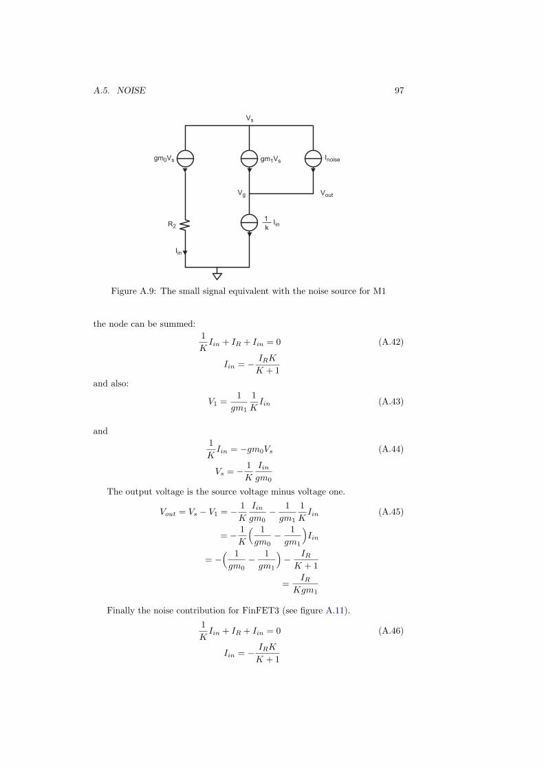
A.5. NOISE 97
k
1
Inoise
R2
Iin
Iin
Vs
gm0Vs gm1Vs
Vg Vout
Figure A.9: The small signal equivalent with the noise source for M1
the node can be summed:1KIin + IR + Iin = 0 (A.42)
Iin = − IRK
K + 1and also:
V1 =1
gm1
1KIin (A.43)
and1KIin = −gm0Vs (A.44)
Vs = − 1K
Iingm0
The output voltage is the source voltage minus voltage one.
Vout = Vs − V1 = − 1K
Iingm0
− 1gm1
1KIin (A.45)
= − 1K
( 1gm0
− 1gm1
)Iin
= −( 1gm0
− 1gm1
)− IRK + 1
=IR
Kgm1
Finally the noise contribution for FinFET3 (see figure A.11).
1KIin + IR + Iin = 0 (A.46)
Iin = − IRK
K + 1

98 APPENDIX A. THE PTAT VOLTAGE GENERATOR
k
1Inoise
R1
R2
Iin
Iin
gm0Vs
k
1Iin
V1
-
+
Vs
Vout
Figure A.10: The small signal equivalent with the noise source for M2
and also:
V2 = Iin1
gm1(A.47)
= − IRK
K + 11
gm1
and
Iin = Vsgm0 (A.48)
Vs =Iingm0
For the output voltage holds:
Vout = Vs + V2 =Iingm0
+Iingm1
(A.49)
=( 1gm0
+1
gm1
)− IRK
K + 1
=( 1Kgm1
+1
gm1
)− IRK
K + 1
=(K + 1Kgm1
)− IRK
K + 1
=IRgm1
So the equation for the total noise in one section of the PTAT voltagebecomes:
V 2noise,tot = V 2
noise,m0 + V 2noise,m1 + V 2
noise,m2 + V 2noise,m3 (A.50)
V 2noise,tot = (
Inoise,m0
gm0)2 + (
Inoise,m1
gm1)2 + (
Inoise,m2
kgm1)2 + (
Inoise,m3
gm1)2

A.5. NOISE 99
k
1Inoise
R1
R2
Iin
Iin
gm0Vs
Iin
V2
-
+
Vs
Vout
Figure A.11: The small signal equivalent with the noise source for M3

100 APPENDIX A. THE PTAT VOLTAGE GENERATOR
A.5.1 Thermal noise
For the thermal noise the equation is (for long devices):
I2noise =
83KTgm (A.51)
So the total thermal noise is:
V 2noise,tot =
83KT
(gm0
gm20
+gm1
gm21
+gm2
k2gm21
+gm3
gm21
)(A.52)
=83KT
( 1gm0
+1
gm1+
gm2
k2gm21
+gm3
gm21
)In this equation can be substituting that:gm2 = Kgm3 and gm0 = Kgm1
This gives:
V 2noise,tot =
83KT
(( 1K
+ 1) 1gm1
+( 1K
+ 1)gm3
gm21
)(A.53)
=83KT
1gm1
(( 1K
+ 1)(
1 +gm3
gm1
))With:gm1 = 40I3 and gm3 =
√2knW3
L3I3 This gives:
V 2noise,tot =
83KT
140I3
(( 1K
+ 1)(
1 +
√2knW3
L3
40√I3
))(A.54)
From this equation the standard deviation could be calculated. This is doneby integrating the noise over a certain frequency range. It is not known tillwhat frequency the thermal noise is constant. The assumption is made thatthis is the case till 1 GHz. So the standard deviation can be expressed withthe following equation:
σ2 =∫ 1GHz
0
V 2noise,totdf (A.55)
= f8KT120I3
(( 1K
+ 1)(
1 +
√2knW3
L3
40√I3
))|1GHz0
Sigma is chosen to be 1mV so from the previous equation the current can becalculated.
I3 = f8KT120σ2
(( 1K
+ 1)(
1 +2
40Vgt3
))(A.56)
From this the I3 can be calculated. So the I2 is then I2 = KI3.
Now that the currents and the k and N are known the device dimensionscan be calculated. Known is that the differential pair is in sub-threshold andthe current mirror in saturation:
Id =W
LId010−10−at+b
expqVgsKbT
(A.57)
Id = knW
L
(Vgs − Vth
)2

A.5. NOISE 101
t is the temperature in degrees Celsius. For this the sub-threshold parameters aand b need to be known. These are determined by measurements a = 1.7510−3
and b = 1.14. The measurement results are shown in appendix A.2.


Appendix B
The CTAT voltage generator
B.1 Sub-threshold FinFET diode
For a diode like behavior in FinFET technology, an exponential term is needed.The FinFET equation for sub-threshold contains an exponent:
ID = 2W
LCgµ0(
kBT
q)2e
q(Vgs−T H)kBT [1− e(
−qVDSkBT )] (B.1)
When Vds is large this approximates to:
ID ≈ 2W
LCgµ0(
kBT
q)2e
q(Vgs−VT H )kBT (B.2)
This looks like an equation for a diode current. It is also important what thenegative temperature coefficient is and wether a PTAT voltage can be gener-ated.
To get the negative temperature coefficient the derivative of the FinFETvoltage in sub-threshold need to be taken to temperature. This is shown inequation B.6.
dVgsdT
=kBqln(
IdIs
) +kBq
13
+dVthdT
(B.3)
In this equation the only factor that is dependent on the device size is:
Is =W
LCgµ0(
kBT
q)2 (B.4)
From the derivative can be seen that the gate-source voltage of a sub-thresholdFinFET has a negative temperature coefficient. An expression for dVth
dT , how-ever is needed.
The positive temperature coefficient is made with the difference in voltagebetween two diodes that have different currentdensities.The current difference is made by different Is and therefore different devicesizes.Id1 = Id2
103

104 APPENDIX B. THE CTAT VOLTAGE GENERATOR
Is2 = nIs1It is assumed that that dVth
dT is device size independent, which means:
dVgs1dT−dVgs2
dT=k
q
[ln(Id1)−ln(Is1)+
kBq
13
+dVth1dT−ln(Id2)+ln(nIs2)−kB
q
13−dVth2
dT]
(B.5)It is assumed that the threshold voltage for both subthreshold FinFETs is
equal. This gives:d(Vgs1 − Vgs2)
dT=k
qln(n) (B.6)
It is thus seen that the positive temperature dependency can be made byusing the voltage difference of two sub-threshold FinFETs that have differentcurrent densities.
A negative and a positive temperature coefficient can be made using sub-threshold FinFET. A disadvantage of using subthreshold FinFETs is that thegate source voltage needs to be lower then the threshold voltage (lower then0.3V for a nFinFET at low temperature). The sub-threshold FinFET is diodeconnected so this means that the CTAT voltage will maximally be 0.3V (1sub-threshold FinFET is used). This is a disadvantage because it is difficult touse in the averaging part of the circuit.The diodes will therefore be made by gated pin diodes.

B.2. DIODE MEASUREMENTS 105
B.2 Diode measurements
A measurement of Salsa 2 gated diode is shown in figure B.1.
Figure B.1: Gated PIN diode measurements on different sized diodes
In the figure the measured I-V curves are shown for different diode sizes.For all measurement the gate is floating. From these curves the width andlength for a certain temperature coefficient and bias current can be chosen.
Also the temperature coefficient a diode has been measured(see figure ??)to verify if the measured temperature coefficient equals the calculated.
The actual diode voltage is approximately 0.58V at 50 0C so the temperaturecoefficient is approximately -1.85mV/K.The negative temperature coefficient can be calculated with:
∂Vbe∂T
=Vbe − (4 +m)KbT
q − VgT
(B.7)
with Eg = 1.12eV and m = 1.5This equation gives the correct temperature coefficient.

106 APPENDIX B. THE CTAT VOLTAGE GENERATOR
Figure B.2: The I-V curves of a diode for different temperatures

Appendix C
The buffer
C.1 Current ratios error
Because of the large voltage difference over the inputs of the differential pairs(at low and high temperatures) the current ratios in the differential pair willbe high. This will give an error on the reference voltage.This error can be described. Because two OTAs are connected together thecurrent can flow from one OTA to the other. This is schematically shown infigure 4.2.
Vref
VptatVctat
IbIbIa
Ib
IaIaIa
IaIaIaIc
Iref Iref DI
Figure C.1: The circuit of the buffer with the different currents
What is known is that the current source is equal to the added current inthe differential pair.Iref = Ia + IbWhat is also known is that the current that flows from one OTA to the otheris equal to:
107

108 APPENDIX C. THE BUFFER
Ic = Ia − Ib
First the error on the reference voltage because of a variation in the currentof one stage can be derived by using the small signal equivalent.
From this circuit first a small signal equivalent for one buffer is made. Infigure C.2 the small signal equivalent of one buffer is shown.
gm0Vgs0
gm2
1
gm1
1
gm3Vgs3
dIVref
Vgs0Vgs3
+
-
+
-
Figure C.2: The small signal equivalent of one buffer stage
The transistors for the current mirror are equal as well as the currents andtherefore holds:gm2 = gm3
This small signal equivalent can be redrawn.
gm0Vgs0gm2
1
gm1
1
gm2Vgs2
dIVref
Vgs0Vgs2
+
-
+
-
gm1
1
gm0
1
Figure C.3: The small signal equivalent of one buffer stage
From this small signal equivalent equations for the gate source voltage of

C.1. CURRENT RATIOS ERROR 109
transistor 0 and 2 can be given:
Vgs0 = −Vref1
gm0
1gm0
+ 1gm1
(C.1)
Vgs2 =gm0Vgs0gm2
= − gm0gm1
gm2(gm0 + gm1)Vref
The error current of one buffer stage can be expressed:
dI =Vref
1gm0
+ 1gm1
− gm2Vgs2 (C.2)
Substituting the gate source voltage of transistor 2 gives:
dI =Vref
1gm0
+ 1gm1
− gm2gm0gm1
gm2(gm0 + gm1)(C.3)
Rewriting this gives the following expression:
VrefdI
=12gm0 + gm1
gm0gm1(C.4)
So one buffer section can be seen as a resistor with:
R =12
( 1gm0
+1
gm1
)(C.5)
Now the small signal equivalent of both buffer stages can be described by thepreviously given small signal equivalent of one stage with the resistor as a loadthat represents the other buffer stage.
The small signal equivalent of this can be seen in figure C.4. The lowersmall signal equivalent is a rewritten version of the upper. The transistors forthe current mirror are equal as well as the currents and therefore holds:gm6 = gm7.
From this the gate source voltages of transistors 5 and 6 can be derived:
Vgs6 =gm5V gs5gm6
(C.6)
Vgs5 =−I3gm5
with:
I3 = I2 − dI (C.7)
I2 =(Vref + Vgs5
)gm4
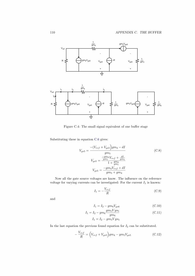
110 APPENDIX C. THE BUFFER
gm5Vgs5
gm7
1
gm4
1
gm6Vgs6 dI
Vref
Vgs6Vgs5
+
-
+
-
R
gm5Vgs5gm6
1
gm4
1
gm6Vgs6 dI
Vref
Vgs6Vgs5
+
-
+
-
R
I0
gm5
1
I1 I2 I3
Figure C.4: The small signal equivalent of one buffer stage
Substituting these in equation C.6 gives:
Vgs5 =−(Vref + Vgs5
)gm4 − dI
gm5(C.8)
Vgs5 =−gm4gm5
Vref + dIgm5
1 + gm4gm5
Vgs5 =−gm4Vref + dI
gm5 + gm4
Now all the gate source voltages are know. The influence on the referencevoltage for varying currents can be investigated: For the current I1 is known:
I1 = −VrefR
(C.9)
and
I1 = I2 − gm6Vgs6 (C.10)
I1 = I2 − gm6gm5V gs5gm6
(C.11)
I1 = I2 − gm5V gs5
In the last equation the previous found equation for I2 can be substituted.
− VrefR
=(Vref + Vgs5
)gm4 − gm5Vgs5 (C.12)

C.1. CURRENT RATIOS ERROR 111
substituting the equation for Vgs5 and rewriting gives:
− VrefR
= Vrefgm4 −(gm5 − gm4
)Vgs5 (C.13)
Substituting Vgs5 (equation C.8) gives:
− VrefR
= Vrefgm4 +(gm5 − gm4
)gm4Vref + dI
gm5 + gm4(C.14)
Rewriting this to Vref :
Vref = dI
gm5−gm4gm5+gm4
1R + gm4 + gm5−gm4
gm5+gm4
(C.15)
Rewriting gives:
VrefdI
=(gm5 − gm4
gm5 + gm4
)( 11R + gm4
)+
1gm4
(C.16)
For the matching in the buffer FinFets M0 and M4 have to be equal andhave the same current as well as M1 and M5:
gm0 = gm4 (C.17)gm1 = gm5
R =12
( 1gm0
+1
gm1
)The previous equation can therefore be simplified:
VrefdI
=(gm1 − gm0
gm1 + gm0
)( 12gm0gm1gm0+gm1
+ gm0
)+
1gm0
(C.18)
To simplify the previous equation:
dI
Vref=(gm1 + gm0
gm1 − gm0
)( 2gm0gm1
gm0 + gm1+ gm0
)+ gm0 (C.19)
=3gm0gm1
gm0 − gm1+
gm20
gm0 − gm1+ gm0
This gives:
VrefdI
=1
gm0
(4gm1
gm1−gm0
) (C.20)
The intend for this calculation was to find an expression for the error onthe reference voltage because of the current ratio. So the gm terms have to besubstituted with:
gm0 =√
2knIa (C.21)
gm1 =√
2knIb
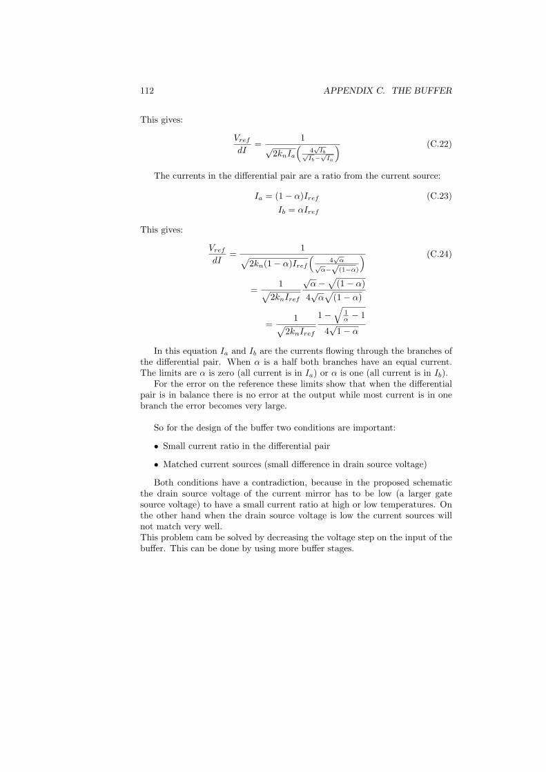
112 APPENDIX C. THE BUFFER
This gives:
VrefdI
=1
√2knIa
(4√Ib√
Ib−√Ia
) (C.22)
The currents in the differential pair are a ratio from the current source:
Ia = (1− α)Iref (C.23)Ib = αIref
This gives:
VrefdI
=1√
2kn(1− α)Iref(
4√α
√α−√
(1−α)
) (C.24)
=1√
2knIref
√α−
√(1− α)
4√α√
(1− α)
=1√
2knIref
1−√
1α − 1
4√
1− α
In this equation Ia and Ib are the currents flowing through the branches ofthe differential pair. When α is a half both branches have an equal current.The limits are α is zero (all current is in Ia) or α is one (all current is in Ib).
For the error on the reference these limits show that when the differentialpair is in balance there is no error at the output while most current is in onebranch the error becomes very large.
So for the design of the buffer two conditions are important:
• Small current ratio in the differential pair
• Matched current sources (small difference in drain source voltage)
Both conditions have a contradiction, because in the proposed schematicthe drain source voltage of the current mirror has to be low (a larger gatesource voltage) to have a small current ratio at high or low temperatures. Onthe other hand when the drain source voltage is low the current sources willnot match very well.This problem cam be solved by decreasing the voltage step on the input of thebuffer. This can be done by using more buffer stages.