design of an automated validation environment for … · design of an automated validation...
TRANSCRIPT

Design of an Automated Validation Environment For
A Radiation Hardened MIPS Microprocessor
by
Abhishek Sharma
A Thesis Presented in Partial Fulfillment
of the Requirements for the Degree
Master of Science
Approved June 2011 by the
Graduate Supervisory Committee:
Lawrence Clark, Chair
Aviral Shrivastava
Keith Holbert
ARIZONA STATE UNIVERSITY
December 2011

i
ABSTRACT
Ever reducing time to market, along with short product lifetimes, has
created a need to shorten the microprocessor design time. Verification of the
design and its analysis are two major components of this design cycle. Design
validation techniques can be broadly classified into two major categories:
simulation based approaches and formal techniques. Simulation based
microprocessor validation involves running millions of cycles using random or
pseudo random tests and allows verification of the register transfer level (RTL)
model against an architectural model, i.e., that the processor executes instructions
as required. The validation effort involves model checking to a high level
description or simulation of the design against the RTL implementation. Formal
techniques exhaustively analyze parts of the design but, do not verify RTL against
the architecture specification.
The focus of this work is to implement a fully automated validation
environment for a MIPS based radiation hardened microprocessor using
simulation based approaches. The basic framework uses the classical validation
approach in which the design to be validated is described in a Hardware
Definition Language (HDL) such as VHDL or Verilog. To implement a
simulation based approach a number of random or pseudo random tests are
generated. The output of the HDL based design is compared against the one
obtained from a "perfect" model implementing similar functionality, a mismatch
in the results would thus indicate a bug in the HDL based design. Effort is made
to design the environment in such a manner that it can support validation during
ii
different stages of the design cycle. The validation environment includes
appropriate changes so as to support architecture changes which are introduced
because of radiation hardening. The manner in which the validation environment
is build is highly dependent on the specifications of the perfect model used for
comparisons. This work implements the validation environment for two MIPS
simulators as the reference model. Two bugs have been discovered in the RTL
model, using simulation based approaches through the validation environment.

iii
ACKNOWLEDGMENTS
First of all, I would like to thank my parents and family for the support
they have given throughout my studies. They have stood by me through the ups
and downs of my graduate life and I am really grateful for that.
I would like to thank my advisor Dr. Lawrence Clark, for the guidance and
support that he has given me throughout my masters. I also thank Dan Patterson
for his guidance on the subject matter. I also take this opportunity to thank Dr.
Keith Holbert and Dr. Aviral Shrivastava for being on my committee.
I would also like to thank Brian Gaeke, OVPsim administrators for
answering all my questions on VMIPS and OVPsim respectively, and my
colleagues Shravan Lakshman, Anubhav Gupta and Satendra Maurya for their
technical and non-technical ideas without which the successful completion of the
work would not have been possible.

iv
TABLE OF CONTENTS
Page
LIST OF TABLES .............................................................................................. vi
LIST OF FIGURES ........................................................................................... vii
CHAPTER
1 INTRODUCTION ........................................................................... 1
1.1 Functional Verification Using Random Test Generation ........... 2
1.1.1 Basic Framework ..................................................... 2
1.1.2 Testing Strategy ....................................................... 5
1.1.3 Correctness Checking .............................................. 8
1.1.4 Coverage Analysis ................................................. 10
1.2 Performance Validation ......................................................... 11
1.3 Organization.......................................................................... 12
2 MIPS ARCHITECTURE AND EMULATORS ............................... 14
2.1 MIPS Architecture ................................................................. 14
2.1.1 Execution Pipeline ................................................. 15
2.1.2 Addressing ............................................................ 17
2.1.3 Modes of Operation and Segments ......................... 18
2.1.4 Registers ............................................................... 20
2.1.5 Instruction Set ....................................................... 21
2.1.6 Exceptions ............................................................. 22
2.1.7 Translation Lookaside Buffers (TLB) ..................... 24
2.2 MIPS Emulators .................................................................... 27

v
CHAPTER ` Page
2.2.1 VMIPS .................................................................. 27
2.2.2 OVPsim ................................................................ 29
3 VALIDATION ENVIRONMENT DESIGN .................................. 34
3.1 Random Instruction Generator ............................................... 37
3.1.1 Generating Biased Instructions ............................... 37
3.1.2 Initial Setup ........................................................... 40
3.1.3 Region of Operation .............................................. 47
3.1.4 Configuring Various Instructions ........................... 51
3.1.5 Instruction Hazards ................................................ 60
3.1.6 Testing the Memory Management Unit (MMU) ..... 61
3.2 Testbench Input Generation for RTL Model ........................... 63
3.3 Design of the Execution Comparator ...................................... 66
3.3.1 Types of Errors ...................................................... 66
3.3.2 Methodology ......................................................... 67
3.3.3 Special Conditions ................................................. 69
3.4 Test Automation .................................................................... 70
4 RESULTS AND CONCLUSIONS .................................................. 72
4.1 Statistics from the Random Instruction Generator.................... 72
4.1.1 Statistics from the First Test ................................... 73
4.1.2 Statistics from the Second Test............................... 74
4.1.3 Statistics from the Third Test ................................. 78

vi
CHAPT ER Page
4.2 Configuring Tests for Processor Validation ............................ 79
4.3 Conclusions........................................................................... 81
REFERENCES ................................................................................................ 83
APPENDIX
A Copyright Permission from MIPS Technologies .......................... 85

vii
LIST OF TABLES
Table Page
1. General Exception Vector Addresses .............................................. 22
2. Statistics from the First Test .......................................................... 74
3. Statistics from the Second Test ........................................................ 76
4. Statistics from the Third Test ........................................................... 79

viii
LIST OF FIGURES
Figure Page
1.1 Static Random Instruction Generation (SRIG) Work Flow. ............. 3
1.2 Methodology to Generate Test Vector for Corner Cases .................. 7
1.3 Performance Validation Methodology Overview ........................... 12
2.1 Processor Core Block Diagram for MIPS-4kc Core ....................... 14
2.2 Virtual to Physical Memory Mapping in MIPS. ............................. 19
2.3 JTLB Entry (Tag and Data) ........................................................... 25
3.1 Flow for Random Tests ................................................................ 35
3.2 Weight File to Test Logical and Branch Instructions...................... 39
3.3 Perl Code to Generate Biased Random Instructions. ...................... 40
3.4 Reset Handler for Uncacheable Accesses ...................................... 42
3.5 Exception Handler for Testing with VMIPS .................................. 45
3.6 Exception Handler for Testing with OVPsim ................................. 46
3.7 Random Test Setup for Testing in Kseg1 ....................................... 48
3.8 Random Test Setup for Testing in Kseg0 ....................................... 50
3.9 Assembly code for Copying Data .................................................. 50
3.10 Incorrectly Configured Jump Instruction. ...................................... 54
3.11 Correctly Configured Jump Instruction. ......................................... 56
3.12 Convergence Issues in Branch and Jump Instructions .................... 57
3.13 Directed Tests to test MMU. .......................................................... 61
3.14 TLB Miss Handler. ........................................................................ 63
3.15 Output Trace Obtained from OVPsim. ........................................... 65

ix
Figure Page
4.1 Frequency Comparison for First Test. ............................................ 75
4.2 Frequency Comparison for Second Test. ....................................... 77
4.3 Frequency Comparison for Third Test. .......................................... 78

1
Chapter 1
INTRODUCTION
The complexity of modern processors has made functional verification a
huge bottleneck for large scale designs, which consequently affects the time to
market [Poe, 2002]. A general agreement among many observers is that
verification consumes at least 70 percent of the design effort [Zhongshu, 2003].
Today‟s methodology for designing microprocessors involves modeling at various
levels of abstraction [Bose, 1999]. These abstractions range from initial
performance only models used in the pre-synthesis phase, to final stage, detailed
register transfer level (RTL) models. The RTL model, which is coded in a
hardware description language such as VHDL or Verilog, captures the intended
functionality and cycle to cycle timing of the entire design. This model is
subjected to validation using simulation based approaches to ensure the RTL
executes the Instruction Set Architecture (ISA) as specified. The validated RTL
model then serves as a reference model for the circuit level description of the
processor [Bose, 1999]. At this stage, standard formal verification tools may be
used. This thesis focuses on the RTL vs. architectural model comparison stage.
In the late 1990 the emphasis was primarily on performance modeling. At
this high level of abstraction, the primary target of the designer was to define the
microarchitecture, which implements a given instruction set architecture with
lowest CPI (cycles per instruction). However, with designs which use millions of
transistors and run at gigahertz clock frequencies, there is a need to include lower
level design constraints into early-stage, high-level modeling and analysis.

2
Generally the top level of abstraction is the ISA level functional model.
The performance-only simulation model models the microarchitectural
implementation of ISA, but is limited to capturing correct timing behavior. The
bottom level of abstraction is the RTL model, which captures both the
functionality and timing associated with design. This said pre-silicon validation
encompasses two primary tasks, first is verifying functional correctness at the
architectural level, which involves verifying that the implemented design properly
captures the functional semantics of the source ISA. Second is the performance
verification, which makes sure that clock cycle time meets estimated projections.
1.1 Functional Verification Using Random Test Generation
1.1.1. Basic Framework
Random test generation is a common technique used for processor
functional verification. It has the ability to reduce the functional verification
efforts and the time to market [Zhongshu, 2003]. Static random instruction
generation (SRIG) is a widely used methodology. Figure 1.1 shows the basic flow
in SRIG. The SRIG tool generates an assembly code based on predefined
configuration options. The cross-compiler and linker convert this assembly code
into object code, this object code serves as the input to the emulator and RTL. An
emulator serves as a reference model and is expected to mimic the design
functionality perfectly. This emulator is generally written in a high level language
such as C/C++ and the highest possible performance is desirable. After the

3
Figure 1.2.Static Random Instruction Generation (SRIG) Work Flow
simulation of two models, results are compared through a checker and any
mismatches are reported. In SRIG workflow the assembly level random test is
generated prior to simulation. This can result in some potential disadvantages. For
example, branch instructions might be difficult to support in this scheme since it
is difficult to make sure that there is some code resident at the branch target, and
even if there is, branch to a previous code, i.e. one that occurs higher in the
instruction flow, might result in an infinite loop. Another issue is to control
indirect accesses to memory. In most processors memory is divided into pre
defined regions meant for special tasks such as read only portion, I/O cached
portion. Since the register value is random in nature, it requires a lot of extra
effort to control memory accesses. Some other issues that plague SRIG are its
Figure 1.1. Static Random Instruction Generation (SRIG) work flow. After
[Zhongshu, 2003]

4
inefficiency in finding bugs in earlier stages of the simulation cycle as desired,
and its dependence on the disk storage capacity which limits test size.
To alleviate these problems a Dynamic Random Instruction Generation
(DRIG) methodology can be adopted as suggested in [Zhongshu, 2003]. In a
DRIG type generator, instructions and random data in machine code are generated
according to a seed variable. During the simulation, when the Device Under Test
(DUT) requires instruction or data, modules in Programming Language Interface
(PLI) are called to fetch the required instruction or data. The collected data is then
issued to the RTL and the emulator. When the instruction completes, the
processor state is determined, and is compared with the results from the reference
model.
A DRIG based verification methodology offers several advantages over a
SRIG based methodology. Since the instruction is generated in machine code
format, it does not need to run the assembler and linker. The simulation can be
stopped automatically at a test point when two designs do not match. This saves
considerable time when the design is big, particularly for debug.
A functional verification effort in which pseudorandom testing was used
with some hand generated tests to produce first pass working parts of the Alpha
21164 CPU chips is described in [Kantrowitz, 1995]. The strategies used in the
verification of Alpha 21164 serve as basic guidelines for any validation scheme in
today‟s microprocessor design and are summarized here. The validation effort
should make sure that every block of logic and every function in the chip has been
exercised completely, i.e. in all modes to ensure that no serious functional bugs

5
remain in the design. In the Alpha 21164 CPU chip the RTL model was
implemented in the C language. The verification team employed several
techniques to ensure full functional verification of the chip. The primary
technique was use of pseudorandom tests. Pseudorandom tests were generated,
and executed on both the Alpha 21164 model and a reference model, and the
results compared. The second important technique was use of focused, hand
written tests to cover specific areas of logic [Kantrowitz, 1995].
The validation effort was implemented in three parts. In the first phase,
during the early stages of the project, the main goal was to exercise as much
design functionality as possible. This ensured that as the design is stabilized, most
major bugs were uncovered. This approach has an additional advantage for the
design team, which could begin physical design as major revisions will not be
required. Once the design is stabilized the verification team needed to create a test
plan. The test plan should capture all the features of the design that need to be
tested, including any special features that might be application specific. The final
verification step is to decide what mechanism is best suited for a particular block
in the design, pseudorandom testing or handwritten focused testing.
1.1.2. Testing Strategy
The test stimulus includes both focused tests and pseudorandom tests.
Pseudorandom testing helps in generation of test cases that might be tedious to
hand generate and are of multiple simultaneous events that would be extremely
difficult to foresee. The pseudorandom testing can be divided into several parts.
One can be a general purpose exerciser that provides coverage of the entire

6
architecture. Others target specific blocks in the architecture. The following areas
are critical to correct functionality of any chip and should be targeted explicitly:
Branches and jumps,
Data pattern dependent transactions,
Floating point unit,
Exceptions,
Cache and memory transactions, and
Virtual to physical address translation mechanism
Fundamentally, each part works the same way. Each exerciser creates
pseudorandom assembly language code, runs the code on the model under test
and a reference model, collects results from each and compares the results from
both the model runs. The only difference in the exercisers is the difference in the
number of certain events or instructions in the generated pseudorandom code. For
example an exercise that focuses on testing the memory transactions will have a
higher number of loads and stores in the generated code. The instructions that are
in majority in the generated code are controlled by variables that are user inputs to
the generator.
It is quite possible that both pseudorandom testing and hand written tests
may not exercise a bug. This might be possible when the bug is the result of the
interaction of corner cases in several different parts of a complex design. A
typical example is one that actually occurred in the MIPS R4000PC/SC rev 2.2
processor. This bug occurs when a data cache miss is caused by a load instruction,

7
and is followed by a jump instruction with its delay slot on an unmapped page.
The bug was that instead of page miss exception vector, processor control was
transferred to jump address [Ho, 1995]. Hand written tests are not effective in
finding such errors because every possible interaction cannot be guaranteed.
Random testing might find such corner cases, but since each condition is highly
improbable the number of random tests required can be prohibitively high. Data
published in [MIPS 94] shows that most of the errors that escape present day
verification methodologies occur due to interactions of various parts of design in
these corner case situations.
To tackle the problem of testing a microprocessor design in all the corner
cases a methodology adopted in [Ho, 1995] can be used. Figure 1.2 gives the
overview of the process. Test patterns are generated in such a manner so that all
possible interactions of different sub-units can be tested.
Figure 1.2. Methodology to Generate Test Vector for Corner Cases. After [Ho,
1995]

8
When the hardware description of the machine is complete, it is likely to contain
information about the improbable states a machine can transition to. This
information can then be extracted to generate test vectors. The method of
extracting this information can be broken down into three parts. The first step is to
convert the HDL based design to a Finite State Machine (FSM) representation.
Second step in the process is to find all the states of machine that can be reached
from reset. The result of this exercise is a state graph, which contains all the states
and transition edges that the hardware model can attain. The last step is to take the
state graph and generate test vectors that will cause all the possible transitions.
1.1.3. Correctness Checking
A number of mechanisms can be used for checking whether the model
under test responded with the correct output. Hand generated tests often have
comparisons built into them to verify that they generated the expected result.
These are known as self checking tests. However, this type of self checking
mechanism can be extremely difficult to implement for pseudorandom testing.
Consequently, checking mechanisms that work well for both hand generated tests
and pseudorandom tests need to be developed. Some of the mechanisms can be:
checks performed during simulation, checks done automatically every time a
model completes executing, or test specific post simulation checks [Kantrowitz,
1995]. It is imperative that the checking mechanisms are properly adjusted to
eliminate false errors, in order to keep the debug time low.

9
The RTL model can provide checking through assertion checkers.
Assertion checkers make sure that various rules of behavior are not violated at
any time during the execution. Assertion checkers can range from simple to
complex. For example, a simple assertion checker can check for an illegal
transition on a state machine and a complex assertion checker can make sure that
none of the bus protocols are violated. When a test is completed, several checks
need to be done. One simple check is to verify that the test reached its normal
completion and did not end abruptly; this makes sure the validation environment
itself is operating correctly. A variety of other checks can be used, for example a
check can compare the results of running a test on the model and on the emulator.
Information about the state of the model is saved while the test is executing and
then compared with its equivalent from the emulator. State that is compared in
this way can include a trace of the program counter (PC), a trace of updates made
to each architectural register, and the final memory image upon the completion of
test [Kantrowitz, 1995]. There are certain issues that are associated with this
technique. The emulator provides architecturally correct results but lacks support
for timing, pipelining or caching. Hence several features can be difficult to verify
with the emulator.
In the Alpha 21164 architecture, arithmetic traps are imprecise, which
means that they might not be reported with the exact program counter value that
caused them. Even for architectures supporting precise exceptions, since the
perfect model lacks any concept of pipeline depth or timing, it can report traps,
some interrupts and exceptions at a different time than the real design. Arithmetic
10
traps also presented a problem in the Alpha 21164 validation effort because the
destination register can be unpredictable after a trap [Kantrowitz, 1995]. These
effects can make comparison of the real design with the reference model difficult.
Restricting the pseudorandom tests to avoid these instruction sequence or, use of
certain register values limits the benefits of pseudorandom testing. Hence to
maximize benefits from pseudorandom testing, no restrictions should be placed
on the instruction sequence. The mismatches should be filtered by tracking which
registers could be unpredictable at a given time. Commercial tools such as
Synopsys Formality can also be used for equivalence checking [Mishra, 2005].
The tool reads the DUT and the reference model. Both the designs are then
partitioned into sections which can be compared separately. Any mismatches are
then reported.
1.1.4. Coverage Analysis
One of the primary difficulties associated with functional verification is
that it is difficult to determine when the validation effort is complete. Completing
a given number of tests only indicates that the tests are complete, not that the
design has been completely tested. Bug rate might provide some useful insights
but a lower bug rate might also indicate that the testing is not properly exercising
the problem areas [Kantrowitz, 1995]. This entails exhaustive coverage analysis
of focused and pseudorandom tests. This coverage checking can be determined
with information gathered while a model was executing, or information gathered
by post processing signal traces. While the model executes, information can be
stored about the occurrence of simple events. At the end of every run, this

11
information can be written to a database to collect statistics that span over
multiple runs.
Automatic coverage-checking methods can also be used. The most
common is a state machine coverage analyzer [Kantrowitz, 1995]. For state
machines it is imperative to exercise all the possible states in the machine. Trace
files can be post processed to gather information about covered and uncovered
states. To extend this concept to other parts of the machine which are not
implemented as FSM, design can be represented as a single state machine. This
state machine can then act as a reference model and can be processed with
coverage tools.
1.2. Performance Validation
Although the primary focus of validation effort in any microprocessor
design is ensuring proper functionality, pre- silicon performance validation is also
an important aspect of the verification effort. Performance validation ensures
elimination of bugs caused by latent functional defects before the final tape-out
[Bose, 2000]. Architecture performance is usually measured in terms of cycles per
instruction (CPI). The methodology used in performance validation is to first
derive performance bounds associated with a given instruction sequence. This
instruction sequence is then used to generate tests cases for which performance
can be predicted before simulation. The two primary aspects of processor
performance that need to be addressed are: (a) clock frequency target and (b)
cycles-per-instruction target [Bose, 2000]. Figure 1.3 provides an overview of the
methodology used for performance validation.

12
A reference tool generates performance bounds for each test case. The test
cases range from tests that check simple pipeline latencies to test cases that assess
the various bandwidth parameters. Single test cases such as load or store
instructions can be used to check basic pipeline latencies while loop test cases can
be used to test fundamental bandwidth and dependence latency parameters. For
each test case performance parameters obtained from the reference tool are
compared against those obtained from the RTL model.
1.3. Organization
This thesis is structured as follows.
Chapter 1 has described the need for validation in today‟s microprocessor
design and contemporary strategies used in various validation schemes.
Chapter 2 describes MIPS processor and emulators. Two MIPS emulators
are described: (a) VMIPS, which emulates MIPS R-3000, was used in the initial
phase of the validation effort and (b) OVPsim, which accurately emulates MIPS-
4kc
Fi Figure 1.3. Performance Validation Methodology Overview. After [Bose, 2000]

13
based processors and offers several advantages over VMIPS was used in the later
part of the validation effort.
Chapter 3 describes the design of the proposed validation environment for
functional verification of MIPS based radiation hardened processor using
simulation based approaches. At the outset the framework was developed to
support validation using VMIPS. In the later stages the environment was modified
to support OVPsim which allowed testing of all the instructions supported by the
MIPS-4kc architecture except for cache instructions.
Chapter 4 tabulates the statistics associated with the random instruction
generator. This is followed by a description of how random tests were configured
to exercise various components of the design and a summary of bugs found. This
chapter concludes this thesis with directions for future work.

14
CHAPTER 2
MIPS ARCHITECTURE AND EMULATORS
An overview of MIPS architecture and emulators is presented here.
Differences in architectural implementations of MIPS-R3000 and MIPS-4kc
based processors are noted.
2.1 MIPS Architecture
MIPS is one of the most effective Reduced Instruction Set Computer
(RISC) architectures, as is evident from strong MIPS influence on later
architectures like Digital Equipment Corporation Alpha and Hewlett-Packard
Precision [Sweetman, 2002]. Figure 2.1 shows the processor core block diagram
for MIPS-4kc core [MIPS, 2002].
Figure 2.1. Processor Core Block Diagram for MIPS-4kc Core. After [MIPS,
2002]

15
Figure 2.1 includes two types of blocks, required and optional. To remain MIPS-
compliant the processor core should implement the required blocks. The required
blocks are
Execution Unit
Multiply-Divide Unit
System Control Coprocessor (CP0)
Memory Management Unit (MMU)
Cache Controller
Bus Interface Unit (BIU)
Power management
Optional blocks are implementation dependent and can be added as the need
arises. Optional blocks are
Instruction Cache
Data Cache
Enhanced JTAG (EJTAG) Controller
2.1.1. Execution Pipeline
Reduced Instruction Set Computer (RISC) is a design philosophy that
advocates use of simpler and smaller instructions which take roughly the same
amount of time to execute over complex multi cycle instructions. The original
MIPS SPARC and Motorola 88000 CPUs were classic scalar RISC pipelines. Later,
Hennessey and Patterson invented yet another classic RISC, the DLX, for use in their
textbook [Hennessy, 2006]. Each of these designs fetch and attempt to execute one

16
instruction per cycle. During operation each pipe stage works on a single instruction
at a time. Each stage takes a fixed amount of time. Each of these stages consists of
an initial set of flip flops, and combinatorial logic which operates on the output of
these flip flops. The five pipeline stages are
1. Instruction Fetch - During the instruction fetch state, a 32 bit instruction is
fetched from the memory. At the same time the instruction is fetched, the
machine computes the address of the next instruction by incrementing the
address of the instruction just fetched by 4 (since each instruction is 4
bytes). The Address of the current instruction is stored in a special register
called the Program Counter (PC). If the next instruction is a taken branch,
jump or exception, the computation will have to be updated accordingly.
2. Instruction Decode /Register Fetch Cycle - All MIPS instructions have at
most two register inputs. During the decode stage, an instruction is
decoded and the registers corresponding to register source specifiers are
read from the register file. Equality test on registers is done as they are
read, for a possible branch. If the need arises, the offset field of the
instruction is also sign extended in this stage. Possible branch target
address is computed by adding the sign extended offset to the incremented
PC. Instruction decoding is done in parallel with reading registers, which
is possible because the register sepcifiers are at a fixed position in RISC
architecture [Hennessy, 2006].

17
3. Execution/Effective Address Cycle - The Arithmetic Logic Unit (ALU)
operates on the operands prepared in the prior cycle, performing one of the
three functions depending on the instruction type. If the instruction is
memory reference, the ALU adds the base register and the offset to form
the effective address. If the instruction is a register-register instruction, the
ALU performs the operation specified by the ALU opcode on the values
read from the register file. If the instruction is a register-immediate
instruction, the ALU performs the operations specified by the ALU
opcode on the first value read from the register file and the sign extended
immediate field.
4. Memory Access - If the instruction is a load, memory does a read using
the effective address computed in the previous cycle. If it is a store, then
the memory writes the data from the second register read from the register
file using the effective address.
5. Write-Back Cycle - In this cycle the result is written into the register file,
whether it comes from the memory system (for a load) or from the ALU
(for an ALU instruction).
2.1.2. Addressing
The MIPS architecture is divided into two address spaces: a virtual
address space, this consists of all the addresses that can be used in the programs,
and a physical address space, consisting of all the addresses that can be sent on
the address bus [Aggarwal, 2004]. The virtual address space of 4 Gbytes is
18
divided into four segments: kuseg, kseg0, kseg1, and kseg2. The virtual address
consists of segment number and an offset within the segment. In translation of
virtual address to the physical address, the 12 least significant bits of the virtual
address are kept unchanged. In an implementation which uses a memory
management unit and a translational lookaside buffer (TLB), segments can be
further divided into pages of sizes ranging from 4 Kbytes to 16 Mbyte. Figure 2.2
shows various segments in MIPS virtual address space.
2.1.3. Modes of Operation and Segments
MIPS-4kc processor cores support three modes of operation [MIPS, 2002]
User Mode
Kernel Mode
Debug Mode
User mode is primarily used for application programs. Kernel mode is used for
handling exceptions and privileged operating system functions, including
coprocessor zero register management and I/O device accesses. Debug mode is
used for software debugging and occurs within a software development tool. The
address translation performed by the MMU depends on the mode in which the
processor is operating. The core enters kernel mode both at reset and when an
exception is recognized. In kernel mode, software has access to the entire address
space, as well as all CP0 registers. User mode accesses are limited to a subset of
the virtual address space (0x0000_0000 to 0x7fff_ffff) and can be restricted from

19
accessing CP0 functions. In User mode, virtual addresses 0x8000_0000 to
0xfff_fff are invalid and cause an exception if accessed. An unmapped segment
does not use the TLB to translate from virtual to physical address. After reset it is
important to have unmapped memory segments, because the TLB is not yet
programmed to perform the translation. Unmapped segments have a fixed simple
translation from virtual to physical address. Except for kseg0, unmapped
segments are always uncached. The cacheability of kseg0 is set in the K0 field of
the CP0 Config register. A mapped segment uses the TLB to translate from virtual
Figure 2.2.Virtual to Physical Memory Mapping in MIPS
20
to physical address. The translation of mapped segments is handled on a per-page
basis. This translation has information defining whether the page is cacheable,
and the protection attributes that are associated with the page [MIPS, 2002]. The
cacheability of the segment is defined in the CP0 register Config, fields K23 and
KU.
2.1.4. Registers
There are 32 general-purpose registers and 3 special registers on the MIPS
processor. There are also up to 32 registers each on up to four coprocessors. The
processor for which the validation environment is designed, there is only one
coprocessor, coprocessor 0, which is the "system coprocessor"; it takes care of
exceptions and virtual memory issues. Also, since the targeted processor does not
implement the debug mode, coprocessor 0 registers, which are used for debug
purposes, are omitted from the design. In the MIPS architecture register zero is
not writeable and reads always return a zero. However to implement the radiation
hardening aspects, the targeted processor allows writes to register zero. In normal
mode of operation the reads to register zero always return a zero. Processor
returns the actual value that was last written to register zero when processor is in a
new operating mode that is used to correct the processor state after a radiation
error. Any of the 32 general-purpose registers can be used in any instruction that
takes register operands. Register 31 is the "link register". Most of the instructions
for calling subroutines are hardwired to store the return address into this register.
The coprocessor registers can be accessed by using special coprocessor
instructions to move their values to general registers and back.

21
2.1.5. Instruction Set
MIPS instructions can be divided into four groups based on their coding
format [MIPS Ins].
R Type - This group contains instructions that do not use an immediate
field, target offset, or memory address to specify an operand. This includes
arithmetic and logic instructions in which both operands are registers, shift
instructions, and register direct jump instructions (JALR and JR). All R-
type instructions use opcode 000000.
I Type - This group includes instructions with an immediate operand,
branch, load and store instructions. Coprocessor load and store
instructions are also included in this group. All opcodes except 000000,
00001x, and 0100xx are used for I-type instructions.
J Type - This group consists of the two direct jump instructions (J and
JAL). These instructions require a memory address to specify their
operand. J type instructions use opcodes 00001x.
Coprocessor Instructions - This group includes floating point processor
and system coprocessor instructions. All coprocessor instructions use
opcodes 0100xx.
MIPS-4kc based processors have several instructions such as Traps,
ERET, BLTZALL, BNEL etc which are not supported by MIPS-R3000 based
processor. There is also a considerable difference in bit encodings of various CP0
registers when compared to R-3000 based processors. Therefore VMIPS which

22
mimics R-3000 based processors provides only limited testing for MIPS-4kc
processor. CP0 register comparison is also not possible using VMIPS, which is
important especially during exceptions and memory management.
2.1.6. Exceptions
Exceptions are conditions which change the normal sequence of
instructions causing the processor to transfer control to a predefined location in
memory which is the exception vector [Aggarwal, 2004]. In MIPS there is a
single exception vector, the general exception vector, whose virtual address
depends on the setting of the Status Register's Bootstrap Exception Vector (BEV)
bit, as shown in Table 1.
Table 1.General Exception Vector Addresses
The MIPS architecture recognizes several exceptions, they can be external
interrupts (hardware interrupts or software interrupts), or program exception.
When an exception occurs, the following events take place:
The current instruction is aborted, as well as any instructions in the
pipeline that have already begun executing
BEV=1 BEV=0
Virtual Address 0xbfc0_0380(kseg1) 0x8000_0180(kseg0)
Physical Address 0x1fc0_0380 0x0000_0180

23
In the Status register, the previous kernel/user mode and previous Interrupt
Enable (IE) bits are copied into the old mode and old IE bits respectively,
and the current mode and current IE bits are copied into the previous mode
and previous IE bits.
The current IE bit is cleared, which disables all interrupts.
The current kernel/user mode bit is cleared, which places the processor in
kernel mode.
If the instruction executing when the exception occurred is in the delay
slot of a branch, the Branch Delay (BD) bit in the Cause register is set.
The Exception Program Counter (EPC) register is written with the address
at which the program can be correctly restarted. If the instruction that
caused the exception is in the delay slot of a branch (BD=1), the EPC is
written with the address of the preceding branch or jump instruction.
Otherwise, it is written with the address of the instruction that caused the
exception, or in the case of an interrupt, with the address of the next
instruction to be executed.
The Exception Code (ExcCode) field of the Cause register is written with
a number that describes the type of exception.
If the exception is a coprocessor unusable exception, the Cause register's
Coprocessor Error (CE) field is written with the referenced coprocessor
unit number.
If the exception is an address error, the address associated with the
erroneous access is written to the BadVAddr register.

24
The processor then jumps to the general exception vector, whose address
depends on the setting of the BEV bit: When BEV = 1, the general
exception vector lies in noncacheable kseg1 address; when BEV = 0, it is
lies in cacheable kseg0 address
When the exception routine completes, it uses the address in the EPC
register as the return address, and executes an Exception Return (ERET)
instruction. The ERET instruction restores the current, previous mode and IE bits
to their contents prior to the interrupt, leaving the old bits unchanged. The
processor then jumps to the address specified in EPC. In MIPS-R3000 based
processors the address in the EPC register is used as the return address in a jump,
and then a Restore from Exception (RFE) instruction is executed in the jump's
delay slot. This has similar effect as ERET.
2.1.7. Translation Lookaside Buffers (TLB)
The TLB consists of one joint and two micro address translation buffers
[MIPS 2002]:
16 dual-entry fully associative Joint TLB (JTLB)
3-entry fully associative Instruction micro TLB (ITLB)
3-entry fully associative Data micro TLB (DTLB)
The 4Kc core implements a 16 dual-entry, fully associative Joint TLB that maps
32 virtual pages to their corresponding physical addresses. The JTLB is organized
as 16 pairs of even and odd entries containing pages that range in size from 4-
KBytes to 16-MByte into the 4-GByte virtual address space. The purpose of the

25
TLB is to translate virtual addresses and their corresponding Address Space
Identifier (ASID) into a physical memory address. The translation is performed by
comparing the upper bits of the virtual address (along with the ASID bits) against
each of the entries in the tag portion of the JTLB structure. Because this structure
is used to translate both instruction and data virtual addresses, it is referred to as a
“joint” TLB. The JTLB is organized in page pairs to minimize its overall size.
Each virtual tag entry corresponds to two physical data entries, an even page entry
and an odd page entry. Figure 2.3 shows the various JTLB fields in MIPS-4kc
core processor [MIPS 2002].
Following are the TLB tag entry fields
Page Mask [24:13] - is the page mask value. The page mask defines the
page size by masking the appropriate VPN2 bits from being involved in a
comparison. It is also used to determine which address bit is used to make
the even-odd page (PFN0-PFN1) determination. Page mask is set in the
CP0 PageMask register
Figure 2.3. JTLB Entry (Tag and Data). After [MIPS 2002]

26
VPN2 [31:13] - is Virtual page number (VPN) divided by 2. This field
contains the upper bits of the virtual page number. Because it represents a
pair of TLB comparison pages, it is divided by 2. Bits 31:25 are always
included in the TLB lookup. Bits 24:13 are included depending on the
page size, defined by CP0 PageMask register. VPN2 is set in CP0 EntryHi
register.
G - is Global (G) bit. When set, it indicates that this entry is global to all
processes and/or threads and thus disables inclusion of the ASID in the
comparison.
ASID [7:0] - is Address Space Identifier (ASID) which identifies which
process or threads this TLB entry is associated with.
C0 [2:0], C1 [2:0] - bits contain an encoded value of the cacheability
attributes and determines whether the page should be placed in the cache
or not. These bits are set in CP0 EntrlyLo registers.
PFN0 [31:12], PFN1 [31:12] – bits define Physical Frame Number (PFN).
They are the upper bits of the physical address. For page sizes larger than
4 KBytes, only a subset of these bits is actually used. PFN bits are set in
EntryLo registers.
V0, V1 - are Valid (V) bits. When set they indicate that the TLB entry
and, thus, the virtual page mappings are valid. If this bit is set, accesses to
the page are permitted. If the bit is cleared, accesses to the page cause a
TLB Invalid exception. Valid bits are in CP0 EntryLo registers.

27
2.2. MIPS EMULATORS
Processor emulators are used to mimic actual processors. The output
obtained from the emulator is what one would expect if the same input was given
to the processor. Some simulators modeling MIPS processors are:
SPIM: SPIM is simulator that runs MIPS32 assembly language programs.
SPIM provides a simple debugger and minimal set of operating system
services. SPIM does not execute binary (compiled) programs and cannot
run programs compiled for recent SGI processors. MIPS compilers also
generate a number of assembler directives that SPIM cannot process
[SPIM].
VMIPS: VMIPS mimics MIPS-R300. Full cross compiler tool chain is
used with VMIPS and is written in C++.VMIPS was used in the initial
phase of testing and provided only limited testing capability due to
architecture differences in MIPS-4kc and MIPS-R3000 based processors.
OVP-OVP provides MIPS verified models for different versions of MIPS
based processor and provides full support for processor validation and was
extensively used for our validation effort
2.2.1. VMIPS
2.2.1.1. Overview
VMIPS is a virtual machine simulator based around a MIPS R3000 RISC
CPU core [VMIPS]. It is an open-source project written in C++, which is
distributed under the General Public License (GNU). VMIPS, a virtual machine

28
simulator, does not require any special hardware. It has been tested under Intel-
based PCs running FreeBSD and Linux, and a patch has been developed for
compatibility with CompaQ Tru64 Unix on 64-bit Alpha hardware. VMIPS is
based on RISC architecture, its primitive machine-language commands are all
simple to understand. VMIPS can be easily extended to include more virtual
devices, such as frame buffers, disk drives, etc. VMIPS is written in C++ and uses
a simple class structure. VMIPS is intended to be a virtual machine, which its
users can modify easily. It maintains a close correspondence between its
structures and structures which actually appear in modern physical computer
hardware. VMIPS is also designed with debugging and testing in mind, offering
an interface to the GNU debugger GDB by which programs can be debugged
while they run on the simulator. It is intended to be a practical simulator target for
compilers and assembly language/hardware-software interface courses [VMIPS].
2.2.1.2. Running Programs with VMIPS
The first step is to compile the program which requires a MIPS cross-
compiler. VMIPS supports the GNU C compiler; most installations of
VMIPS also have an installation of the GNU C compiler targeting the
MIPS architecture. The easiest interface to the C compiler is through the
`vmipstool' program; to run the MIPS compiler that VMIPS was installed
with, the `vmipstool --compile' command is used.
29
The second step is linking the program with support code. VMIPS comes
with an inbuilt support code and a linker script for simple standalone
programs, which can be run using the command `vmipstool --link'.
The third step is building a ROM image. Like most real machines VMIPS
does not read in executables, it has an embedded program in the flash
ROM that reads the executable and runs it. To build a ROM image,
VMIPS provides a script which is invoked by running `vmipstool --make-
rom'.
The fourth step is starting the simulator using `vmips ROMFILE', where
`ROMFILE' is the name of the ROM image. If the program is linked with
setup code that comes with VMIPS, the simulator halts when it hits the
first break instruction.
2.2.2. OVPsim
2.2.2.1. Overview
OVPsim is developed by Imperas technologies. Imperas simulation
technology is based on just-in-time (JIT) compiler technology and enables high
performance simulation, debug and analysis of platforms containing multiple
processors and peripheral models [OVP1]. OVPsim is a collection of dynamic
linked libraries (.so suffix on Linux, .dll suffix on Windows XP) implementing
Imperas simulation technology. The shared objects contain implementations of
the entire Innovative CpuManager Interface (ICM) interface [OVP2]. These ICM
functions enable instantiation, interconnection and simulation of complex

30
multiprocessor platforms containing arbitrary shared memory topologies. A
program using ICM can be linked with the ICM RuntimeLoader to perform
loading of OVPsim dynamic linked libraries, to produce a stand-alone executable.
The technology is designed to be extensible: one can create new models of
processors and other platform components using interfaces and libraries supplied
by Imperas. Imperas OVPsim allows processor models created using OVP
modeling technology to be used in platform files to create executables that
execute binaries compiled for those processor models. It can also simulate
behavioral components to help validate processor models under construction, or
to create custom simulation environments.
2.2.2.2. Processor Models
The core simulation components in OVPsim are processor models
[OVP1]. In order to implement a processor model, OVPsim implements the
following major components in C using the Imperas Virtual Machine Interface
(VMI) API:
An instruction decoder, capable of decoding a single instruction.
An instruction disassembler, capable of generating a text representation of
an instruction.
An instruction morpher, capable of describing the behavior of a single
instruction.
A debugger interface, which provides functions, required for the model to
be debugged using GDB or the Imperas multiprocessor debugger.

31
If a processor implements virtual memory, then the hardware structures
that support that virtual memory (MMU and TLB, for example) also form
part of the processor models.
Imperas processor models are compiled into a shared object (.so or .dll)
which is then dynamically loaded by Imperas tools.
2.2.2.3. Semihosting
Semihosting allows behavior that would normally occur on a simulated
system to be implemented using features of the host system instead [OVP1]. As a
simple example, a real platform might contain a UART peripheral to receive
output. When simulating this system, it is generally more convenient not to
simulate the UART but to intercept the write calls that a processor makes and
redirect the output to the simulator log instead. Such behavior is specified in a
semihosting library for a processor.
2.2.2.4. Cache and Memory Subsystem Models
Imperas technology allows memory subsystem models such as caches to
be modeled as loadable shared objects (or dynamic linked libraries on Windows)
and separately instantiated [OVP1]. Memory subsystem models can be either full
or transparent. A full model implements memory contents: for example a full
cache model would implement both cache tags and the cache line contents. A
transparent model implements some state but not the memory contents: for
example, a transparent cache model would implement the cache tags but not the
line contents, which is useful for performance analysis models that simply count
hits and misses.

32
2.2.2.5. Running Programs with OVPsim
Programs on OVPsim are executed by calling various ICM functions
[OVP2]. A simple program can be made that runs a single-processor platform
using following five calls from the ICM API.
icmInit- icmInit initializes the simulation environment prior to a
simulation run: it is always the first ICM routine called in any application.
It specifies attributes to control various aspects of the simulation to be
performed, and also specifies how a debugger should be connected to the
application if required.
icmNewProcessor- icmNewProcessor is used to create a new processor
instance. The ISA that the user wants to mimic is specified here.
icmLoadProcessorMemory-Once a processor has been instantiated by
icmNewProcessor, this routine is used to load an object file into the
processor memory. Accepted formats are ELF and TI-COFF. Makefiles
that come with the Imperas setup can be used to create these file formats
from assembly or C programs. Entry point address for simulations can
also be specified in the makefiles.
icmSimulatePlatform- icmSimulatePlatform is used to run simulation of
the processor and program, for a specified duration.
icmTerminate- At the end of simulation, icmTerminate is called to
perform cleanup and delete all allocated simulation data structures.

33
This chapter has described various architecture features of MIPS based
processors which should be kept in mind while designing the validation
environment for MIPS processors. This chapter also provides an overview of
MIPS emulators which form an important part of any validation environment.
Chapter 3 provides details on the design of the validation environment and
a description of how various instructions are configured to test different parts of
the design.
34
CHAPTER 3
VALIDATION ENVIRONMENT DESIGN
This chapter describes the design of the proposed validation environment
for a radiation hardened MIPS processor. The environment can be configured to
run a variable number of tests in a single run, each test in turn can be configured
to run a given number of instructions. Any instruction that is not supported by the
implementation can be eliminated from the random tests. Similarly, a particular
test run may be configured to test only certain types of instructions, for example
arithmetic instructions. Figure 3.1 shows flow for random tests. Design of the
entire validation environment can be divided into five major parts:
1. The first step is to generate a sequence of random instructions. The
instruction generator requires the capability to generate the desired
instruction mix. Although generated randomly, the instruction sequence
should not result in unpredictable processor behavior.
2. The second step is to convert this sequence of assembly level instructions
into a binary format which can be executed by the simulator. This can be
done with a set of appropriate make files. While OVPsim recognizes ELF
format, VMIPS requires that the random tests be converted to a ROM
image. An embedded bootstrap program in the flash ROM reads the
executable and then executes it. The ELF or ROM files that are generated
contain needed information e.g., entry point address for executing the
program. Once the desired file format is generated, these files can be

35
Figure 3.1. Flow for Random Tests

36
executed with the simulator to obtain the expected register file and
Program Counter (PC) values after each instruction executed.
3. The third step is to generate inputs for the Device under Test (DUT),
which is the RTL model. The RTL model requires that each instruction in
random test is converted to a 64 bit field. This 64 bit field comprises of 32
bit physical address which can be placed on the address bus, and 32 bit
binary machine code corresponding to the instruction which is located at
the specified physical address. The validation environment converts
random test into this format. The RTL model is then executed to obtain the
outputs corresponding to the applied stimulus.
4. The fourth step is the comparison of the results obtained from steps three
and four. PC and register file values are compared to ensure that the DUT
is functioning as expected. Any discrepancies found are reported, as they
represent a divergence in the architectural states of the respective machine.
5. The fifth step is to combine all these independent processes into a single
process which can be configured for the desired number of runs. This step
should ensure that all the files needed to run a given test are properly
archived. If any design changes are introduced later, this makes sure that a
test which executed without any discrepancies can be executed again to
ensure that bugs are not introduced during the design change.

37
The following subsections describe the detailed design of each part. The Perl
language is used throughout this work to generate random tests, inputs for the
RTL model, compare results, and to automate the environment for the desired
number of runs.
3.1. Random Instruction Generator
The random instruction generator generates a sequence of pseudorandom
instructions under a given set of constraints. These constraints are given as
command line arguments and through an input file which describes the desired
frequency of each instruction in the random test.
3.1.1. Generating Biased Instructions
The random instruction generator requires the capability to generate
instructions in a biased manner. This implies that if the user assigns a
comparatively higher weight to a particular instruction, that instruction should be
generated more frequently than others in the random test. The frequency of the
instructions is calculated by the weight assigned to each instruction which can be
described in a text file and provided as an input to the random instruction
generator. The ability to generate instructions according to their weights has
several advantages.
During the design phase there might be several instructions which are yet
not supported. With the weight file, simply assigning a zero weight to all these
instructions eliminates them from the random tests. This does not require any
changes in the validation environment. For example, a design which does not

38
implement a multiply/divide unit can have all the multiply/divide instructions
assigned a zero weight for testing purposes. In later stages of the design if a
multiply/divide unit is implemented and needs to be tested, simply assigning
proper weights to the multiply/divide instructions accomplishes this.
A biased random generator also allows us to more rigorously exercise a
particular unit in the design. This is known as “directed” random testing. For
example, if the overflow condition in add instructions needs to be tested, the add
instructions can be assigned a higher weight than the other instructions. Similarly
memory accesses can be tested by assigning higher weights to loads and stores.
The weights for various instructions are specified in a weight file, which
the random instruction generator takes as an input. The weight file contains all the
instructions that are supported by the instruction set architecture. As an example a
test which is required to generate a few logical instructions with branch
instructions will have the weight file set up as shown in Figure 3.2 All the other
instructions will be assigned a zero weight.
The first step in post processing the weight file is to generate a hash with
the instruction as the key and weight of the instruction as the value associated
with it. A hash is a data structure that uses a hash function to map identifying
values, known as keys, to their associated values [Wiki1]. This hash is then
converted to another hash which has the instruction as the key but this time the
probability associated with each instruction as the value associated with the key.
This is done by adding the weights associated with all the instruction to get their

39
sum. The weight of an instruction is divided by this sum to return the probability
of occurrence associated with each instruction. Once this hash is obtained, the
code show in Figure 3.3 taken from the Perl Cookbook [Perl1], is used to generate
instructions pseudo randomly with their weighted bias taken into account.
Weighted_Rand is the subroutine which is called when the instructions need to be
ADD-20
ADDI-20
ADDIU-20
ADDU-20
AND-10
ANDI-10
BEQ-2
BEQL-2
BGEZ-2
BGEZAL-2
BGEZALL-2
BGEZL-2
BGTZ-2
BGTZL-2
BLEZ-2
BLEZL-2
BLTZ-2
BLTZAL-2
BLTZALL-2
BLTZ-2
BLTZL-2
BNE-2
BNEL-2
BREAK-0
CLO-0
CLZ-0
DIV-0
DIVU-0
J-0
Figure 3.2. Weight File to Test Logical and Branch Instructions

40
generated with their bias taken into account. %dist is the hash which contains
instructions and their associated probabilities.
3.1.2. Initial Setup
To properly configure a random test we need to do a few things for
housekeeping.
3.1.2.1. Initializing Register File
First is initializing all the registers to known values before the start of the
actual random test. The VMIPS setup file initializes all the registers to a value
zero. Initializing all the registers to zero will produce zero as the result of most of
the operations; this does not create any operands which might result in corner
cases for the validation purposes. Also, at the RTL level the register file is
modeled as a variable in VHDL, which has an unknown value at the start of
simulation. To address these problems the register file is initialized using the LI
macro and the Perl random function. A random number in a given range is
generated using the rand function in Perl. This random number is then moved to a
given register using LI macro. For example if the random number generated is
Sub Weighted_Rand {my %dist = @_; my ($key,
$weight);
while (1) { # to avoid floating point
inaccuracies
my $rand=rand;
while (($key, $weight) = each %dist) {return
$key if ($rand -= $weight) < 0;} } }
Figure 3.3. Perl Code to Generate Biased Random Instructions

41
0x8000_0300 the LI macro is LI $1, 0x8000_0300. This macro is
implemented as a sequence of LUI and ORI instructions. Register zero cannot be
initialized since it is hardwired to zero. Register 1 (at) is reserved for use by the
assembler ('at' stands for "assembler temporary"). It is used to hold intermediate
values when performing macro expansions. We can prevent the assembler from
using this register with the directive ".set noat". A .set directive should therefore
be used before the register R1 is loaded to avoid any assembler warnings. Before
we start executing the actual sequence of randomly generated instructions, the
proper reset and exception handlers must also be in place to ensure proper
execution
3.1.2.2 Reset Handler
Reset refers to the condition when the system starts from power up on a
hard reset. In the MIPS architecture the CPU responds to reset by starting to fetch
instructions from the virtual address 0xbfc0_0000. This is physical address
0x1fc0_0000 in the kseg1 region. The reset vector is configured in kseg1 because
it is the uncached, unmapped address space. This is important since at the time of
reset neither the caches nor the TLB are initialized. It is imperative that
substantial testing is carried out in kseg0 which comprises of addresses
0x8000_0000 to 0x9FFF_FFFF. Operation in kseg0 allows us to do three things.
Firstly, it allows us to remain in kernel mode, which in turn allows us to execute
all instructions, including privileged ones. Secondly, it allows us to remain in
unmapped memory so we do not have to worry (initially) about creating page
tables and a TLB miss exception handler. Thirdly, since the accesses can

42
configured to be cacheable, operation in kseg0 allows us to test the cache
accesses.
When coming out of the reset handler kseg0 can be configured as
cacheable or uncacheable. The choice to configure kseg0 as cacheable or
uncacheable is an option available to the user and is a command line input to the
validation environment. At the end of the reset handler the processor should jump
to the address where the random test is located. To configure kseg0 as
uncacheable, the assembly language code in Figure 3.4 is used as the reset handler
Following is the line by line description of the code:
(1, 2) Load R2 with the value 0x0000_ff01.
(3) Move the value in R2 (0x0000_ff01) to CP0 Status register. This sets
the IE and IM bits which are the Interrupt Mask and Interrupt Enable bits
and have an unknown value after the reset. This instruction also clears the
BEV bit in the Status register. Clearing the BEV bit makes the general
exception vector location in kseg0 at the address 0x8000_0180. When the
BEV bit is set the general exception vector is located in kseg1 at the
Reset_Handler_Uncacheable:
lui $2, 0x0000 #(1)
ori $2, $2, 0xff01 #(2)
mtc0 $2, CP0_ Status #(3)
lui $2, 0x0000 #(4)
mtc0 $2, CP0_ Cause #(5)
li $2, 0xrandom_test_location #(6)
jr $2 #(7)
nop #(8)
Figure 3.4. Reset Handler for Uncacheable Accesses

43
address 0xbfc0_0380. The benefit of executing the exception routine in
kseg0 is that it can be made to be cacheable there.
(4) Load R2 with the value 0x0000_0000.
(5) Move the value in R2 (0x0000_0000) to CP0 Cause register. This
clears all the bits including the IV bit. When the IV bit is cleared the
interrupt exceptions use the general exception vector.
(6) Load R2 with the address of the first instruction in the random test.
(7) Jump to the first instruction in the random test.
(8) Fill the branch delay slot with a NOP instruction.
To configure kseg0 as cacheable the same reset handler is used with an
additional instruction that loads the value 0x0000_ff01 into CP0 Config register.
This clears the K0 bit of the Config register, configuring all the accesses to kseg0
as cacheable. The RTL model requires a few other instructions in the reset handler
for cacheable access. These instructions are implementation dependent and are
used to invalidate the instruction and data caches at reset (rather than a software
loop as is usual for a MIPS processor).
3.1.2.3. Exception Handler
In the MIPS architecture exceptions are precise. In a precise exception
CPU, exception points to the instruction that is the exception victim. All
instructions preceding the exception victim in execution sequence are complete;
any work done on the victim and on any ensuing instructions have no effect.
44
When a MIPS CPU takes an exception the processor control is transferred to a
fixed address which is the exception vector. The location of the exception vector
depends on the BEV bit of CP0 Status register. If the BEV bit is cleared, the
exceptions are cached and the exception vector is located in kseg0 at the address
0x8000_0180. If the BEV bit is set, then the exceptions are uncached and the
exception vector is located in kseg1 at the address 0xbfc0_0380. For good
performance on exceptions it is desirable to have the interrupt entry point in
cached memory [Sweetman, 2002]. Most of the testing in the validation effort is
done with the BEV bit cleared.
The initial phase of testing was done using VMIPS which mimics R-3000
based MIPS processors. These processors use the RFE (Restore from Exception)
instruction, it restores the status register to make it ready to go back to the state
the processor was in before the exception happened. Since the RTL model does
not implement the RFE instruction, a simple scheme to manually restore the
processor state after the exception is used. The CP0 EPC register stores the
address at which processing resumes after the exception routine has been
completed. Before returning from the exception routine this address should be
incremented by 4 to point it to the instruction following the one which caused the
exception (since each instruction is of 4 bytes), otherwise we will have a flow
where control keeps switching between the exception routine and the instruction
which caused the exception. The assembly code in Figure 3.5 was used when
testing with VMIPS.

45
Following is the line by line description of the code:
(1) Move the address of instruction which caused the exception from CP0
Exception Program Counter (EPC) register to R1.
(2) Increment R1 to point to the instruction following the one which caused
the exception.
(3, 4) Load R2 with the value 0xffff_fffd.
(5) Move content of CP0 register Status to R3.
(6, 7) Move the value in R3 to CP0 Status register. This clears the EXL bit
which implies the processor is in normal mode. When the EXL bit is set the
processor runs in kernel mode and all the interrupts are disabled.
(8) Jump to instruction following the one that caused exception, as specified
by R1
(9) Fill the branch delay slot with NOP instruction.
Exception_Handler_VMIPS:
mfc0 $1, CP0_ EPC #(1)
addiu $1, $1, 0x00000004 #(2)
lui $2, 0xffff #(3)
ori $2, $2, 0xfffd #(4)
mfc0 $3, CP0_Status #(5)
and $3, $3, $2 #(6)
mtc0 $3, CP0_Status #(7)
jr $1 #(8)
nop #(9)
Figure 3.5. Exception Handler for Testing with VMIPS
46
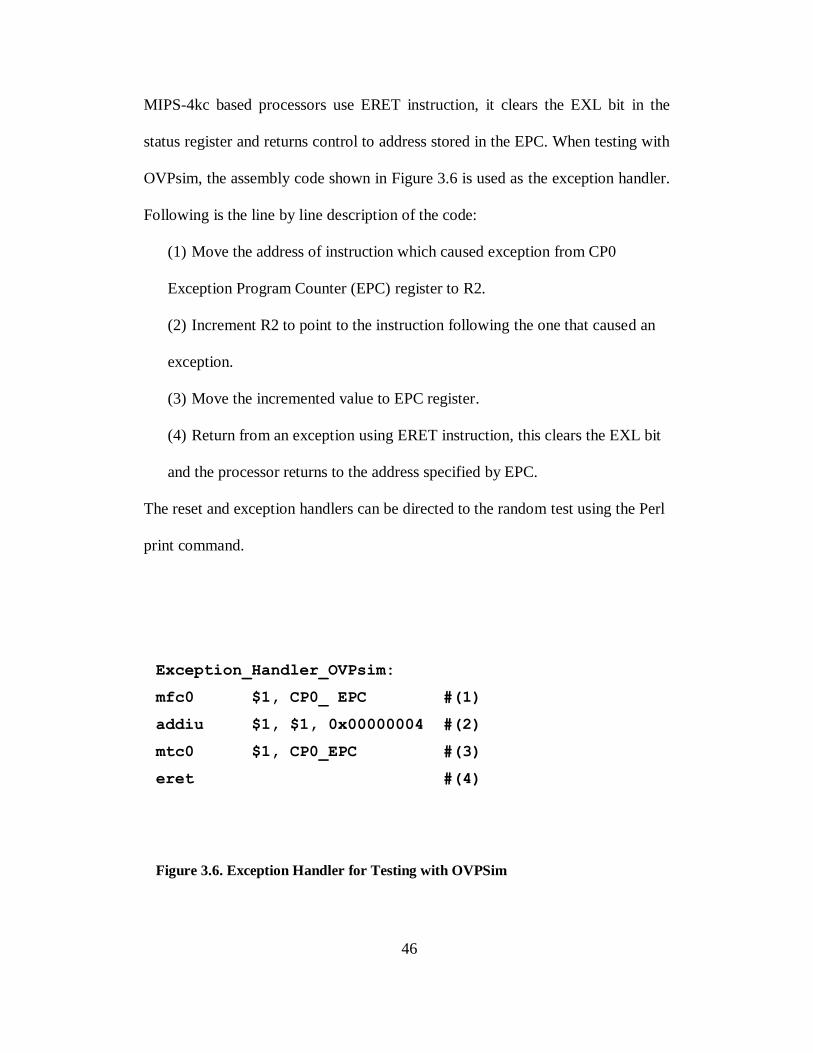
MIPS-4kc based processors use ERET instruction, it clears the EXL bit in the
status register and returns control to address stored in the EPC. When testing with
OVPsim, the assembly code shown in Figure 3.6 is used as the exception handler.
Following is the line by line description of the code:
(1) Move the address of instruction which caused exception from CP0
Exception Program Counter (EPC) register to R2.
(2) Increment R2 to point to the instruction following the one that caused an
exception.
(3) Move the incremented value to EPC register.
(4) Return from an exception using ERET instruction, this clears the EXL bit
and the processor returns to the address specified by EPC.
The reset and exception handlers can be directed to the random test using the Perl
print command.
Exception_Handler_OVPsim:
mfc0 $1, CP0_ EPC #(1)
addiu $1, $1, 0x00000004 #(2)
mtc0 $1, CP0_EPC #(3)
eret #(4)
Figure 3.6. Exception Handler for Testing with OVPSim

47
3.1.3. Region of Operation
Another important issue as previously discussed is deciding in what region
to operate the random tests. From a validation perspective we would want to
operate in all three regions of the MIPS virtual address space. Kuseg which
comprises of addresses ranging from 0x0000_0000 to 0x7fff_fff is mapped
memory space, allows us to test the Memory Management Unit (MMU) which
translates virtual addresses to physical addresses. Kseg0 comprising of addresses
from 0x8000_0000 to 0x9fff_ffff allows us to test all the instructions in kernel
mode with both cached and uncached access, hence allowing us to test caches.
Kseg1 comprising of addresses from 0xa000_0000 to 0xc000_000 allows us to
test uncached and unmapped addresses. Methodology to operate in kseg0 and
kseg1 is described in the following subsections. Operation in kuseg is discussed
separately, since it requires a TLB miss handler for virtual to physical address
translation.
3.1.3.1. Kseg1 Operation
From an implementation perspective, kseg1 is the simplest region. In
MIPS architecture the entry point after the reset is in kseg1 at the address
0xbfc0_0000. This is also the default entry point or start address for VMIPS.
Hence the reset handler would be at this address. With the BEV bit set, the
exception vector is at the location 0xbfc0_0380. In assembly language .org
directive can be used to specify offsets from a start address (only forward offsets
are allowed with .org meaning the address should increment). Since the start

48
address in this case is 0xbfc0_0000, the exception vector is at an offset of 0x380.
Once the initial set up is done, the random test can be conveniently specified at a
desired address with the offset specified by .org directive. If the user prefers to
load the random test at the address 0xbfc0_0500 then the entire test setup of the
random test is shown in Figure 3.7. Following is the line by line description:
(1) Start defines the entry point address, 0xbfc0_0000 in this case.
(2) Assembly code for reset handler as shown in Figure 3.4.
(3) Jump to first instruction in the random test which is at the location
0xbfc0_0500.
(4) This defines an offset of 0x380 from entry point address for the exception
handler.
(5) This is the assembly code for exception handler as show in Figure 3.6
(6) This defines an offset of 0x500 from entry point address for the first
instruction in random test.
(7) Start of the random test.
.globl start__ # (1)
Assembly Code for Reset Handler # (2)
Jump to 0xbfc0_0500 # (3)
.org 0x380 # (4)
Assembly code for Exception Handler # (5)
.org 0x500 # (6)
Random Test # (7)
Figure 3.7. Random Test Setup for Testing in Kseg1.

49
If all the instructions are configured correctly the test should finish at the last
instruction. To ensure the test halts, a break instruction is used as the last
instruction of the test with VMIPS. With OVPsim either a Wait instruction can be
used or global symbol exit can be defined, the simulator halts when it encounters
this symbol.
3.1.3.2. Kseg0 Operation
When operating in kseg0 there are some problems that need to be
addressed. With VMIPS since the entry point is fixed at 0xbfc0_0000 there must
be some way to load the random test at the desired address in kseg0. If the BEV
bit in Status register is cleared the exception vector is located at 0x8000_0180 and
the exception handler should also be loaded at this address. The .org directive
cannot be used to specify the offsets for kseg0 operation since the entry point
address in kseg1 is greater than kseg0 addresses and negative offsets are not
allowed.
To resolve this issue a simple approach is to first configure the test as
operating in kseg1. This datum is then copied from kseg1 addresses to the desired
address location in kseg0. After the data are copied to the address location in
kseg0, the processor jumps to this address location and the random test is then
executed in kseg0. For this we need to have three addresses. First is the start
address from where data are to be copied. Second is the end address up to which
data are to be copied. Third is the destination address to which data needs to be
copied. The start and end addresses for copying can be easily obtained by

50
declaring global symbols at the start and end of the data to be copied. The
destination address is specified
by the user and has to be fixed before configuring the test. For example the global
symbols are declared in Figure 3.8. Following is the line by line description:
(1, 2) Global symbol Random_Test_Start corresponds to the first
instruction in random test.
(3, 4, 5) Global symbol Random_Test_End corresponds to the last
instruction in random test.
Once these symbols are defined, the assembly code shown in Figure 3.9 is used to
copy data to the destination address.
.globl Random_Test_Start # (1)
Random_Test_Start: # (2)
Code for Random Test # (3)
.globl Random_Test_end # (4)
Random_Test_End: # (5)
Figure 3.8. Random Test Setup for Testing in Kseg0
la $1, random_test_start # (1)
la $2, random_test_end # (2)
addiu $2, $2, 4 # (3)
la $3, 0xdestination_address# (4)
a0:
lw $4, 0($1) # (5)
sw $4, 0($3) # (6)
addiu $1, $1, 4 # (7)
addiu $3, $3, 4 # (8)
bne $1, $2, a0 # (9)
nop # (10)
Figure 3.9. Assembly Code for Copying Data.

51
Following is the line by line description of the code:
(1) Load the address of first instruction in the random test in R1.
(2) Load the address of last instruction in the random test in R2.
(3) Increment the address in R2 to one word past the end address.
(4) Load R3 with the destination address. This address is defined by the user.
For kseg0 operation, the address 0x8000_0300 is used in the validation
environment.
(5) Load the data from the source address into R4.
(6) Store the data in R4 to the destination address.
(7) Increment source address, so that it points to next word to be copied.
(8) Increment destination address.
(9) Loop until all the data are copied.
(10) Fill the branch delay slot with NOP instruction.
Although the problem of loading data in a kseg0 is solved by this
methodology, it complicates the way branches and jumps are handled. This is
discussed further in the section on handling various instructions. The problem of
copying data from kseg1 to kseg0 for operation in kseg0 is eliminated when
executing with OVPsim. OVPsim lets the user define the entry point. When
executing in kseg0 this entry point can be conveniently defined as 0x8000_0100
and, an approach similar to that used for operation in kseg1 can be used.

52
3.1.4. Configuring Various Instructions
Once an instruction is generated with the weight bias taken into account,
we need to configure the instruction with the proper operands. For the purpose of
designing a random instruction generator, MIPS instructions can be divided into
the following groups.
3.1.4.1. Register-Register and Register Immediate Instructions
These instructions use either two registers as their inputs or a register and
an immediate field as the input. The output of the instruction is written back to
another register. To randomly choose a register for these instructions, the Perl
rand function can be used to randomly generate an integer between 1 and 31.
Register zero is not chosen, since in the RTL model register zero is writeable
while in simulator register zero is hardwired to zero. Writes to register zero,
implement special radiation hardening features in the RTL. Hence, choosing
register zero would result in unnecessary mismatches when checking the tests.
The immediate field can be generated by randomly choosing an integer between 0
and the maximum range, allowed for a particular instruction. For example if we
consider an ADD instruction which has the format ADD Rx, Ry, Rz where Ry
and Rz are the input registers and Rx stores the result.
$Rx=int rand 32; #Choose a random number between 1 and 31
$Ry=int rand 32; #Choose a random number between 1 and 31
$Rz=int rand 32; #Choose a random number between 1 and 31
This instruction can then be directed to the random test using print command in
the following manner
Print “ADD\s \$$Rx,\$Ry,\$Rz \n”;

53
If $Rx, $Ry and $Rz had values 22, 14, 12 assigned to them respectively then the
ADD instruction will be printed as ADD $22, $14, $12. For an ADDI instruction,
register Rz is replaced by an immediate field.
3.1.4.2. Branches and Jumps
Branches and jumps are the most difficult instructions to be configured in
the random tests. Branches and jumps need to have target addresses. If the branch
condition evaluates to true, the processor fetches the next instruction from the
target address. In case of a jump the control is unconditionally transferred to the
target address. To ensure that we do not cause exceptions in the delay slot all
branches and jumps are followed by a NOP instruction. The following issues need
to be addressed for branches and jumps to ensure a reliable flow.
3.1.4.2.1. Target Addresses
Targets for branches and jumps are placed after every 30 instructions. The
first instruction in the random test begins with the symbol a0, after every 30
instructions this symbol is incremented and printed. For example:
a0:
30 Assembly Instructions
a30:
30 Assembly Instructions
a60:
30 Assembly Instructions
Ideally, all the branches and jumps that appear in the random test can have a0 or
a30 as their target address. However, this might result in an infinite loop. For
example if a jump instruction appears after a60 and the target address is a30, the
control will keep switching back and forth resulting in an infinite loop. One way

54
to ensure that no such infinite loops occur is to use branch and jump targets that
always take the flow in forward direction. This is ensured by a counter which
counts the number of random instructions that have already been generated. For a
forward branch or jump the number associated with the target address (30 for a30)
should be greater than the total number of instructions generated. If a branch is
generated as 70th
instruction a0, a30, a60 would all fail this condition ensuring no
infinite loops are formed.
Another interesting aspect of dealing with jumps and branches is the case
when the target of a jump or a taken branch is another jump or branch. In most of
the cases this should be fine, but when the target instructions are JR or JALR this
can be a problem. JR and JALR instructions use a register as an input. This
register must first be loaded with the appropriate destination address before the
actual instruction is executed. To load the appropriate address into the register, the
la macro is used. For example consider the sequence of instructions shown in
Figure 3.10. The assembler calculates the address associated with a30 by adding
appropriate offset to the entry point. The LA macro then loads this address into
register R3. Once the JR instruction after a0 is executed the control is transferred
a0:
la $3, a30
jr/jalr $3
add $4, $4, $5
la $5, a60
a30:
jr $5
Figure 3.10. Incorrectly Configured Jump Instruction

55
to a30, at a30 there is another JR instruction, the LA macro that precedes the jump
instruction at a30 never gets executed and the processor behavior is unexpected. It
is important to note here that the only problematic case is when the JR or JALR
instruction is chosen as the 29th
instruction. Since, in this case LA macro will be
the 29th
instruction and the jump instruction will be the 30th
, this sequence of
instruction can result in infinite loop. To avoid this problem the following
methodology is used.
Since the targets are chosen randomly, all the taken targets are stored in an
array (for example if an instruction like BEQ $1, $1, a120 is generated,
a120 will be a taken target). Let the variable count denote the sequence of
instruction that will be generated. (If count is 29, we will be generating the 29th
instruction). If count+1 matches any of the taken destinations in the array, then
the current instruction cannot be a JR or JALR. Referring to the previous
sequence we will have 30 stored in the array since it is a taken destination. Now at
the 29th instruction the condition mentioned above will evaluate to true and no JR
or JALR instructions will be generated. When count is 30, condition will evaluate
to false, if JR or JALR is the generated instruction the sequence of instruction
will be as shown in Figure 3.11. This sequence of instruction will work correctly;
once the control is transferred to a30, LA macro will load the correct address in
R2 before the Jump. To make the implementation simpler, another approach

56
could be to avoid JR/JALR instruction every time (count+1) is divisible by 30.
(Since all the possible jump or branch destinations are multiples of 30).
3.1.4.2.2. Use of Labels and La Macro
As mentioned in the previous sections, for operation in kseg0 with VMIPS
the approach is to copy data from kseg1 to kseg0 and then jump to the appropriate
address in kseg0. The problem with this approach is for jumps, la macro and
labels cannot be used. This is due to the fact that when the program is compiled,
all the labels a0, a30 correspond to kseg1 address. For example when operating in
kseg0 if we had a jump instruction J a150, the processor would jump to address
corresponding to a150 in kseg1. Similarly for JR and JALR instructions the la
macro loads the kseg1 addresses into the registers. After the jump instruction, all
execution takes place in kseg1. To address this issue when copying data from one
region to other, actual instruction addresses are used instead of labels. For
example, if a branch target is a60, this will be at an offset of 240 bytes from the
entry point address (since each instruction is of 4 bytes and a60 would imply 60
instructions after the entry point). Once a target is randomly chosen, it is
converted to the equivalent hex address and then used in jumps and branches.
a0:
la $3, a30
jr/jalr $3
add $4, $4, $5
a30:
la $2, a60
jr $2
Figure 3.11. Correctly Configured Jump Instruction

57
3.1.4.2.3. Convergence Issues
When generating tests which contain branches and jumps, if not
configured correctly, the random instruction generator might fail. Consider the
random test containing 1000 random instructions as shown in Figure 3.12. The
label a990 is printed once 990 instructions are generated. After a990 there is not
any possible branch or jump target which will take the flow in the forward
direction. Similarly after a960 the only possible branch or jump target is a990. If
the random test allowed branches and jumps to be generated after a990, the test
generation will never complete because the condition to generate forward target
will be never met.
Random_Test_Start:
a0:
30 random instructions
a30:
30 random instructions
a960:
30 random instructions
a990:
10 random instructions
Random_Test_End:
Figure 3.12. Convergence Issues in Branch and Jump Instructions
Only One Forward
Target Available
No Forward Targets
Available

58
When configuring tests with a large number of instructions, before the last
label only one label will pass the condition for forward targets out of a large set of
possible values. This might take some time to converge to the right value. To
avoid this problem tests are configured in such a manner that the last 60
instructions are never branches or jumps. This way we always have more than one
target available in the forward direction.
3.1.4.3. Loads and Stores
Loads and stores are another class of instructions that need to be
configured properly to ensure a correct flow. All the testing that involved loads
and stores is done using OVPsim. Tests are configured in such a manner that
loads from uninitialized memory locations always return zero both in the RTL
model and the simulator. The first step in handling loads and stores is to define
regions for memory accesses. For example when executing in unmapped space
without the TLB miss handler, two separate regions for memory accesses can be
defined one in kseg1 and another in kseg0. The address range can be either fixed
or can be standard inputs from user.
In the MIPS architecture, before a load or store the destination address
needs to be loaded in a base register. The base register can be randomly chosen,
however care must be taken that the base register is not R0, since R0 is hardwired
to zero. A load or store instruction is always preceded by the LI macro which
loads the base register with appropriate address. Depending on the number of
regions to be accessed a random number could be used to decide what region to
access. For example if user specified kseg0 and kseg1, and the random number

59
generated is 0, kseg0 will be used for memory accesses and vice versa. Once a
region is chosen, address within that region can be chosen randomly to be loaded
into the base register. Unaligned memory accesses result in address exceptions
and the control is transferred to the general exception vector. In the validation
environment the user can choose to generate unaligned memory accesses. This is
provided as a command line input option. The tests are configured in such a
manner that even when requested, unaligned exceptions are only a fixed percent
of total accesses. To generate 20 percent unaligned accesses a random integer can
be chosen between 0 and 4, every time it is equal to 4 an unaligned access is
generated. Similarly when another random number is found to be equal to 0 when
the possible values are from 0 to 4, a store to a memory location is followed by a
load from the same memory location.
Similar to branches and jumps if a load or store instruction is the target of
taken branch or jump then the instruction which loads the base register with
appropriate address might not get executed and we will have an unexpected
processor behavior. The methodology discussed previously for JR and JALR
instructions can be adopted here. Every time the variable count+1 is divisible by
30, the current instruction cannot be a load or store.
3.1.4.4. Trap Instructions
When testing with OVPsim, trap instructions are handled as a register-
register or register-immediate instruction. In the MIPS R-3000 the instruction set
did not yet have any of the trap instructions. When executing with VMIPS, each
time the simulator encounters a trap instruction an exception is taken, and the

60
control is transferred to the general exception vector. To provide some limited
testing of trap instructions using VMIPS, the trap instructions were configured in
such a manner so that the condition for the exception always evaluated to be true.
This way both VMIPS and the RTL model took an exception and the PC trace
was identical for both of them. As an example, if we consider the trap instruction
TEQI, $2,0xfff. The processor will take an exception if the value in R2 is
equal to 0xfff. In the random test this instruction configured as
li $2,0xfff
teqi $2,0xfff
This ensures that the condition for the trap always evaluates to true. Again, this
has similar issues as discussed in branches, jumps, loads and stores. In this case
the random instruction generator must make sure that the trap instruction is never
executed without the LI instruction being executed first; otherwise the PC trace
from simulator will not match the trace from the RTL model.
3.1.5. Instruction Hazards
In general, the MIPS architecture ensures that the processor implements a
fully sequential programming model. Each instruction in the program should see
the results of all the previous instructions. To implement this model, in multicycle
instructions like multiply and divide, a scheme called hardware interlocking is
used. Hardware interlocking ensures that newer instructions are held until older
instructions drain out of the pipeline and write back their results. There can be
some exceptions to this model; these exceptions are referred as instruction
hazards. In the random generator instruction hazards can be avoided by storing

61
the random instruction that was previously generated. If the current random
instruction and the previous instruction form an instruction hazard appropriate
number of NOP instructions are added before the current instruction in the
generated assembly code.
3.1.6. Testing the Memory Management Unit (MMU)
To test the MMU directed tests are used in combination with random tests.
For the directed tests several mappings are defined: Entrylo0, Entrylo1 and
EntryHi are set up accordingly. Once these registers are set up a TLB entry is
written using the instructions tlbwr/tlbwi. This is followed by consecutive stores
and loads to the virtual address, the virtual address is chosen such that it would
need the TLB entry created for the virtual to physical address translation. Figure
3.13 shows the assembly code to test MMU using directed tests.
#define entryhi_00 0x00002000 # (1)
#define entrylo0_00 0x00000014 # (2)
#define entrylo1_00 0x00000054 # (3)
li $2, entryhi_00 # (4)
mtc0 $2, $10 # (5)
li $2, entrylo0_00 # (6)
mtc0 $2, $2 # (7)
li $2, entrylo1_00 # (8)
mtc0 $2, $3 # (9)
li $2, 0x00000000 # (10)
mtc0 $2, $5 # (11)
tlbwr # (12)
li $4, 0x0000_2000 # (13)
li $2, 0x0fff_0f0f # (14)
sw $2, 0($4) # (15)
lw $3, 0($4) # (16)
Figure 3.13. Directed Test to Test MMU

62
All the pages are marked as Global, Valid and Dirty meaning pages are valid,
writeable and no address space ID comparisons are done to obtain the virtual to
physical mapping. Following is the line by line description of the code:
(1, 2, 3) This defines the mapping which is used in the directed test. These
values are moved to CP0 registers EntryHi, EntryLo0, EntryL01 before
writing the TLB entry.
(4) Load the value entrhi_00 into R2.
(5) Move the value in R2 to CP0 EntryHi register.
(6) Load the value entrylo0_00 into R2
(7) Move the value in R2 to CP0 EntryLo0 register.
(8) Load the value entrylo1_00 into R2.
(9) Move the value in R2 to CP0 EntryLo1 register.
(10) Write 0 to R2
(11) Move the value in R2 to CP0 register PageMask. This means we are
doing 4 kbyte pages.
(12) Write a Random TLB entry.
(13) Load R4 with the value 0x0000_2000.
(14) Load R2 with the value 0x0fff_0f0f.
(15) Store the value 0x0ffff_0f0f to virtual address 0x0000_2000.
(16) Load the value stored at virtual address 0x0000_2000 in R3.
Random tests require a TLB miss handler. The reset handler is modified to store
the page mappings at an unmapped address. At the end of reset handler the
processor jumps to an address in kuseg, which is in mapped memory. On the first

63
access, this causes an address exception and the processor jumps to TLB miss
handler which is located at 0x8000_0000 when the EXL bit is clear. The TLB
miss handler then creates the appropriate entry in the TLB for virtual to physical
mapping. The processor then returns to the address in kuseg and the random test
is executed. Figure 3.14 shows the assembly code used as the TLB miss handler.
Following is line by line description of the code:
(1) Load R4 with the address where page tables are located.
(2, 3) Load the mappings to R2 and R3.
(4) Move the value in R2 to CP0 EntryLo0 register.
(5) Move the value in R3 to CP0 EntryLo1 register.
(6) Write the TLB entry, EntryHi is already set up.
(7) Return from exception.
3.2. Testbench Input Generation for RTL model
Once a random sequence of instructions is generated, the assembly code is
compiled and converted into ELF format or a ROM file so that it can be executed
with the simulator. The simulator is then invoked to execute the assembly code
and if the test is configured correctly the simulator halts after the test execution.
li $4,0xpage_table_location # (1)
lw $2, 0($4) # (2)
lw $3, 8($4) # (3)
mtc0 $2, CP0_Entrylo0 # (4)
mtc0 $3, CP0_Entrylo1 # (5)
tlbwr # (6)
eret # (7)
Figure 3.14. TLB Miss Handler

64
The output obtained from the simulator contains the PC trace and the values of all
the registers after each instruction. The output also contains the 32 bit binary code
for each instruction. Figure 3.15 shows the output obtained from OVPsim. The
Instruction Disassemble field shows the PC value and the instruction. The
Memory Dump field is the machine code of the instruction. Register Dump shows
the value of all the general purpose and CP0 register after the instruction is
executed. To generate inputs for RTL from this trace, a Perl program is used to
extract the PC value and the instruction machine code. The program counter value
is then converted to its corresponding physical address. When executing in
mapped space, this requires simple bit manipulation. However, when the address
lies in the mapped space the corresponding virtual to physical address translation
must be known to generate the correct physical address. Once both physical
address and the machine code are known, they are converted to their binary
formats to form a 64 bit field (32 bits each for machine code and physical
address). This 64 bit field is generated for all the instructions in the output trace to
form a text file. This text file is then fed to the RTL model using VHDL File I/O
method, which reads in the text file and stores all the values in array. Since the
array size cannot be dynamic, the size of the text file needs to be fixed. If the
actual number of instructions executed is less than the fixed number (this will be
the case in for tests which include branch and jump instructions) the rest of the
space can be filled by NOP instructions. The last instruction of the text file is
always a WAIT instruction which causes the RTL model execution to be

65
suspended. Additionally, VHDL assertions are used to issue a message indicating
the test was completed successfully.
** Instruction Disassemble
0x80000000 : lui v0,0x0
** Memory Dump
Address 0x80000000 data 0x0000023c
** Instruction Execution
** Register Dump
zero at v0 v1 a0 a1 a2 a3
R0 00000000 00000000 00000000 00000000 00000000 00000000 00000000 00000000
t0 t1 t2 t3 t4 t5 t6 t7
R8 00000000 00000000 00000000 00000000 00000000 00000000 00000000 00000000
s0 s1 s2 s3 s4 s5 s6 s7
R16 00000000 00000000 00000000 00000000 00000000 00000000 00000000 00000000
t8 t9 k0 k1 gp sp s8 ra
R24 00000000 00000000 00000000 00000000 00000000 00000000 00000000 00000000
sr lo hi bad cause pc
00400004 00000000 00000000 00000000 00000000 80000004
fsr fir
00000000 00000000
sr=0x00400004
bad=0x00000000
cause=0x00000000
index=0x00000000
random=0x00000000
entrylo0=0x00000000
status=0x0000ff01
itaglo=0x00000000
idatalo=0x00000000
errorepc=0x00000000
Figure 3.15. Output Trace Obtained from OVPsim
66
3.3. Design of the Execution Comparator
Once the random test is executed on both the RTL model and the
simulator and the output traces are available from both the models, a scheme
needs to be designed to compare the outputs from both the models. This is the part
where any errors in the design are uncovered. The comparison scheme should be
designed in such a manner that any mismatches which result due to
implementation differences are not reported to reduce the verification time.
3.3.1. Types of Errors
The comparator used in the validation environment is designed to report
the following mismatches to the user. First, the comparator should make sure that
the Program Counter trace in both the emulator and the RTL model is identical.
For example if we consider an add instruction, if an overflow condition occurs,
the processor would take an exception and the control would be transferred to the
general exception vector. If this condition is not modeled correctly in the RTL
model, an exception will not occur. In such a case PC trace will be different in the
RTL model and the simulator and a mismatch will be reported to the user.
Secondly, the comparator reports any change in the general or CP0 register
values without change in the PC value. A constant PC value would indicate that
no new instructions are fetched. Therefore, no change in any of the general
purpose or CP0 registers should take place. Third, for a given PC value,
mismatches in any of the general purpose or the CP0 registers are reported.

67
3.3.2 Methodology
The comparator reads the output traces from the RTL model and the
simulator and reports any error found. The input to the comparator is the PC value
from which the user wants to start comparisons. This is important because the
initial set up is different in the two models. When configuring kseg0 for cacheable
accesses the RTL model uses special instructions to invalidate the data cache and
instruction cache which are implementation dependent and are not present in the
MIPS-4kc core. If comparisons are done for PC values when these instructions
are executing, the comparator will report unnecessary mismatches. Usually the
starting address for comparisons is the instruction from which the general purpose
registers are initialized. The output trace is read by the comparator sequentially
and the PC value is extracted. This is compared against the PC value obtained
from the user. If the value matches, a check flag is set, else the comparator
increments to find the next value of PC. Other fields which are required for
comparisons, such as general purpose register values, are not extracted till the
check flag is set, this saves some execution time.
The data structure primarily used for comparisons is the Perl hash. Each
value in hash has a unique key, implying two hash keys can have identical values.
At the start several hashes are declared to hold different values from the output
files. For example to store PC values two hashes are declared, PC_S and PC_R,
the letter S and R denoting that these values come from the simulator and the
RTL, respectively. Similarly R00_S, R00_R are used to store R00 values from the
two models, R01_S, R01_R to store R01 values and so on. Once the check flag is

68
set, a count value is initialized which acts as key for all the hashes. This entails
two counters which can act as keys for the hashes obtained from the two models,
in the comparator the counters are declared as key_rtl and key_simulator. PC
value cannot be used as key because a given PC might have several occurrences
in the test. For example a test which is configured to test trap instructions will
have several occurrences of the general exception vector. For every Program
Counter value encountered after the check flag is set, the counter is incremented
by one. At the end of the extraction process, we will have different hashes with all
the values required for comparison.
The RTL model might have two consequent occurrences of a PC value.
For example let‟s say the in the RTL output, the PC value 0x8000_0500 occurred
thrice in a row. Whether this constitutes an error is implementation dependent. In
the current comparator scheme this is flagged as an error only if any of the
register values change. The comparator checks if the current PC value matches
the previous PC value, if yes and any changes are found, an error is issued,
following which all the hashes are updated with the most recent value of the
registers.
Once we have all the hashes, the comparisons between the values obtained
from the two models are made. First the hashes containing PC values are
compared. If for a given key the PC value from both the emulator and RTL
match, comparisons on all the register values are done for this key. If the value
does not match, an error is issued since this would mean that PC sequence differs
in the RTL model and the simulator. The simulator key is then incremented to

69
find the next matching PC value. In this manner, more than one error can be
found per test.
As an example, assume the key values used to iterate the hashes are
initially 0 for both simulator and RTL. Also, assume that in PC_R the hash values
associated with the keys 0 and 10 are 0x8000_0300 and 0x8000_0180
respectively. Similarly in the PC_S hash, values associated with the keys 0 and 10
are 0x8000_0300 and 0x8000_0340, respectively. Two counters rtl_check and
simulator_check are initialized to zero. The values from the hashes PC_R and
PC_S are read and compared, since they match for key number 0, comparisons on
all the other registers are done. If any mismatch is found error is issued, once all
the comparisons are done both the counters are incremented by one. When both
rtl_check and rtl_simulator equal to 10, a mismatch in PC values is found, this is
reported to the user and the rtl_simulator counter is incremented in the hope of
finding a matching PC value.
3.3.3 Special Conditions
The comparator must make sure that mismatches that occur due to
architecture differences are not reported to the user. In the current implementation
checking is disabled for following cases. If a register value obtained from the
RTL model is either „X‟ or, „U‟ checks are disabled on that register, since this
would imply that the particular register has not been initialized in the RTL model.
In the MIPS architecture an instruction is said to be committed if it is guaranteed
to complete [Hennessy, 2006]. The trace obtained from the RTL model contains
PC values only for the instructions which are committed. An instruction which

70
will cause an exception will never commit and hence will not be seen in the RTL
output trace. However, these instructions appear in the trace from the simulator. If
an instruction at PC 0x8000_0500 caused an exception, the comparator would
complain that PC value 0x8000_0500 is not found in the RTL output trace. To
avoid these errors, the comparator checks if the next PC value in the sequence
matches the general exception vector value, if yes the checks are disabled. When
coming out of the exception handler, the RTL value always has two occurrences
of the instruction following the one which caused an exception. On the first
occurrence the processor control is returned to the following instruction, and on
the second occurrence the instruction is executed. This results in register value
change without change in the PC value. To avoid such errors the comparator
checks if the previous instruction executed is the last instruction of the exception
handler, if the condition is found to be true, checking is disabled for that
occurrence. Since both VMIPS and OVPsim ignore cache instructions, checking
of CP0 registers taglo and datalo is disabled. Finally, if tests are generated to test
unaligned memory accesses, the CE field of Cause register has an unknown value
on an address exception, consequently this check is disabled for tests which
include unaligned memory accesses.
3.4. Test Automation
Once a framework to run a single random test is complete, the whole
process can be configured to run multiple tests at time. This is achieved by using a
shell script which invokes all the individual processes described above
sequentially. The number of tests that are to be executed is provided as command

71
line input by the user along with other options such as whether to configure kseg0
as cacheable, an option to generate unaligned memory accesses. The output of the
exercise is the comparison results for all the tests in the run.
This chapter has described the design of the validation environment for two
MIPS emulators OVPsim and VMIPS. Chapter 4 tabulates statistics obtained
from the biased random instruction generator along with a summary of bugs
found in the design. This chapter concludes this thesis with directions for future
work.

72
CHAPTER-4
RESULTS AND CONCLUSIONS
This chapter is divided into three parts. First part (sub-section) presents the
statistics obtained from the random instruction generator for different instruction
mix. The second part presents an overview of how tests were configured to
exercise various components of the design and an overview of bugs found in the
design. The third part concludes this thesis with directions for future work.
4.1. Statistics from the Random Instruction Generator
This section presents statistics obtained from the random instruction
generator. Three random tests were generated with different mix of instructions.
The weight file was used to assign different weights to the instructions. The first
two were configured to run 100,001 random instruction, the third for 10,001
random instruction (this test included branch instructions, the branch offset is a 16
bit field which might not support all the possible targets when executing 100,001
instructions). The random test results obtained were post processed to obtain the
probability with which each instruction appeared in the random test. The random
test was then converted to ELF format and was executed with OVPsim. The
output trace obtained from OVPsim was post processed to obtain the total number
of instructions executed and the probability of execution associated with each
instruction. This included instructions which were executed during exceptions but
not during the reset handler and initialization of the register file. Following is the
description and results obtained from each test.

73
4.1.1. Statistics from the First Test
First test contained 10 different instructions, each instruction with a
weight of either 10 or 20 with a total of 100,001 random instructions. The output
trace obtained from OVPsim showed that a total of 102,178 instructions were
executed. The overflow condition in add instruction caused 544 exceptions. This
is evident from the fact that output trace from OVPsim contains 544 occurrences
of ERET and ADDIU instructions, both of which are used in the exception
handler. The probability of execution obtained from test execution is different
from probability obtained from random test on account of higher number of
instruction executed due to generated exceptions. Table 2 shows the statistics
associated with this test. The „Weight‟ column shows weight assigned to each
instruction in the weight file along with the probability associated with it (this is
the probability with which an instruction was to be generated in the random test),
the „Frequency (G)‟ column shows number of times that particular instruction
appeared in the random test along with the probability with which it was
generated. „Frequency (E)‟ column shows number of times that particular
instruction was executed with the probability with which it was executed. It
should be noted here that the sum of the column Frequency (E) column is not
102,178 in this case since all the instructions used in the exception handler are not
listed.

74
Figure 4.1 compares the frequency with which different instructions were
requested, generated and executed in the first test.
4.1.1. Statistics from the Second Test
The second test consisted of loads and stores along with other instructions.
The test was configured in such a manner, that a store to a memory location was
always followed by a load from the same memory location.
Table 2. Statisitcs from the First Test
Instruction
Weight Frequency (G) Frequency (E)
ADD 10 (0.0625) 6343 (0.06342) 6343 (0.0621)
ADDI 20 (0.125) 12350 (.1235) 12350 (.1209)
ADDU 10 (0.0625) 6103 (0.06103) 6103 (0.05972)
AND 10 (0.0625) 6279 (0.06279) 6279 (0.06145)
ANDI 10 (0.0625) 6245 (0.06245) 6245 (0.0611)
NOR 20 (0.125) 12417 (0.12417) 12417 (0.1215)
OR 20 (0.125) 12551 (0.12551) 12551 (0.1228)
ORI 20 (0.125) 12543 (0.12543) 12543 (0.1227)
SUBU 20 (0.125) 12569 (0.12569) 12569 (0.123)
XOR 20 (0.125) 12601 (0.12601) 12601 (0.1233)
ADDIU 0 (0) 0 (0) 544 (0.0053)
ERET 0 (0) 0 (0) 544 (0.0053)

75
Figure 4.1. Frequency Comparison for First Test
All the memory accesses were aligned at the word boundary. Table 3 shows the
statistics associated with this test. The total number of instructions generated was
100,001. This included the LI macro which was used to load the base register
with the address of the memory location to be accessed. The load instruction
which immediately followed the store instruction did not use the LI macro
because in that case the base register was already set up. Subtracting the number
of SW instructions (3487) from the LW instructions (6970) will give us the number
of LW instructions which were not preceded by a SW instruction.
0
2000
4000
6000
8000
10000
12000
14000
Requested
Generated
Executed
Fre
qu
ency

76
Subtracting the number of SW instructions (3487) from the LW instructions (6970)
gives us the number of LW instructions which were not preceded by a SW
instruction. This turns out to be 3483 (6970-3487). The number of LI macros we
would expect will be the sum of standalone LW and SW instructions. The sum is
6970 (3483+3487) which is the total number of LI instructions generated in the
Table 3. Statisitcs from the Second Test
Instruction Weight Frequency (G) Frequency (E)
AND 20 (0.167) 14962 (0.1496) 14962 (0.1398)
ANDI 20 (0.167) 14859 (0.1485) 14859 (0.1389)
CLO 20 (0.167) 15137 (0.1513) 15137 (0.1415)
CLZ 20 (0.167) 14925 (0.1492) 14925 (0.1395)
LW 5 (0.041) 6970 (0.0697) 6970 (0.0651)
SW 5 (0.041) 3487 (0.03487) 3487 (0.0325)
NOR 10 (0.083) 7572 (0.0757) 7572 (0.0707)
OR 10 (0.083) 7482 (.07482) 7482 (0.0699)
SUBU 10 (0.083) 7637 (0.07637) 7637 (0.07139)
LI 0 (0) 6970 (0.0697) 0 (0)
LUI 0 (0) 0 (0) 6970 (0.06516)
ORI 0 (0) 0 (0) 6966 (0.06512)

77
random test. The LI instruction is executed as a combination of LUI and ORI
instructions, so the LI instruction does not appear in the output trace obtained
from OVPsim. The difference in number of ORI and LI instructions can be
attributed to the fact that depending on the immediate value, the LI instruction
can be executed only as LUI instruction. The total number of instructions
executed was 106,967 which is the total of the column „Frequency (E)‟. Figure
4.2 compares the frequency with which different instructions were requested,
generated and executed in the second test.
Figure 4.2. Frequency Comparison for Second Test
0
2000
4000
6000
8000
10000
12000
14000
16000
18000
Requested
Generated
Executed
Fre
qu
ency

78
4.1.3. Statistics from the Third Test
Third test consisted of two branch instructions BEQ and BNE along with other
instructions. The test was configured to generate 10,001 random instructions. In
order to avoid exceptions in the branch delay slot, all branch instructions had a
NOP instruction in the delay slot. Figure 4.3 compares the frequency with which
different instructions were requested, generated and executed in the third test. The
total number of instructions executed was only 172. This can be attributed to the
fact that a taken branch will take the flow in forward direction and tests are not
executed sequentially. Table 4 shows statistics from third test.
Figure 4.3. Frequency Comparison for Third Test
0
200
400
600
800
1000
1200
1400
1600
1800
Requested
Generated
Executed
Fre
qu
en
cy
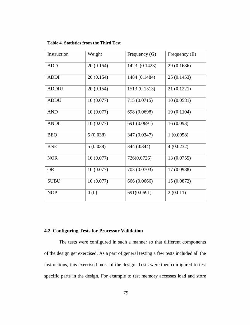
79
4.2. Configuring Tests for Processor Validation
The tests were configured in such a manner so that different components
of the design get exercised. As a part of general testing a few tests included all the
instructions, this exercised most of the design. Tests were then configured to test
specific parts in the design. For example to test memory accesses load and store
Table 4. Statistics from the Third Test
Instruction Weight Frequency (G) Frequency (E)
ADD 20 (0.154) 1423 (0.1423) 29 (0.1686)
ADDI 20 (0.154) 1484 (0.1484) 25 (0.1453)
ADDIU 20 (0.154) 1513 (0.1513) 21 (0.1221)
ADDU 10 (0.077) 715 (0.0715) 10 (0.0581)
AND 10 (0.077) 698 (0.0698) 19 (0.1104)
ANDI 10 (0.077) 691 (0.0691) 16 (0.093)
BEQ 5 (0.038) 347 (0.0347) 1 (0.0058)
BNE 5 (0.038) 344 (.0344) 4 (0.0232)
NOR 10 (0.077) 726(0.0726) 13 (0.0755)
OR 10 (0.077) 703 (0.0703) 17 (0.0988)
SUBU 10 (0.077) 666 (0.0666) 15 (0.0872)
NOP 0 (0) 691(0.0691) 2 (0.011)
80
instructions were assigned higher weights. Different tests focused on testing the
following parts of the design (instructions corresponding to each part were
assigned higher weight to accomplish this)
Arithmetic and logical instructions
Memory accesses
Branches and jumps
Trap instructions
Execution in mapped memory space to test the TLB instructions
Cache accesses by configuring kseg0 as cacheable
Two bugs have been found till now
This bug affects both SLT and SLTI, both of which treat their operands as
signed two's complement integers. The bug was that the logic failed to
account for the overflow case for these instructions. The RTL model
handled the instruction in the following manner where the bug was found
(the instruction was SLT $9, $12, $5):
temp <- R12 - R5
R9 <- "0000000000000000000000000000000" & temp (31)
The sign bit of the result of the subtraction was used to set or clear the
LSB of the destination register. In this case, the operation was
0x0000000000A0 - 0x80000000. In decimal, this is 160 - (-2^31) = 2^31
+ 160. If registers were wider than 32 bits, this could have been
represented as a positive number (in which case the sign bit would be 0).

81
Instead, it results in a negative number, and thus an overflow case. SLTU
and SLTIU were being handled correctly which are the unsigned versions.
This bug affects the TGE, TGEI, TLT, and TLTI trap instructions. The
test uncovered the bug in two places, with the following instructions:
TLT t1, v0 (t1= 0x65ff_f552, v0=0x8000_0a02)
TLT t1, a0 (t1=0x00e0_003d, a0=0x8000_039c)
In both cases, the RTL took an exception when it should not have. The
TGE, TGEI, TLT, and TLTI instructions should treat their operands as
signed integers. The RTL model was incorrectly treating them as unsigned
integers.
4.3. Conclusions
This thesis has presented a methodology to design a robust automated
validation environment for MIPS-4kc based processors. The validation
environment has the capability to generate assembly level random tests with
appropriate bias for different instructions, convert these instructions into a format
which can be executed with the RTL model and the simulator, and as a final step
compare the results obtained from the RTL and the emulator. This environment
can be used to validate any MIPS-4kc based processor. A few changes might be
required in the way inputs are provided to the design under test since this is
implementation dependent.
The simulators used in this implementation ignore cache instructions;
therefore none of the cache instructions and CP0 registers used for caches could
be tested. A capability to test cache instructions would go a long way in designing

82
a foolproof validation environment. Another missing piece in the implementation
is the coverage analysis. Due to lack of appropriate coverage analysis tools, there
was no data on coverage. Running a certain number of instructions gives us no
idea on how much of the design has been exercised and what portions of the
design need to be tested to achieve requisite coverage. Therefore, an ability to test
cache instructions along with the coverage data would make this validation
environment complete.

83
REFERENCES
[Poe, 2002] E. A. Poe, “Introduction to Random Test Generation for
Processor Verification” Technical Report, Obsidian
Software, 2002.
[Zhonsghu, 2003] L. Zhongshu, Y. Xiaolang, W. Jiebing and X. Zhihan, “A
Dynamic Random Instruction and Stimulus Generation for
Functional Verification of Embedded Processor,”
Proceedings of the 5th International Conference on ASIC,
October 2003.
[Bose, 1999] P. Bose, T. Conte, and T.Austin, “Challenges in Processor
Modeling and Validation.” IEEE Micro, pages 2–7, June
1999.
[Kantrowitz, 1995] M. Kantrowitz, L. Noack, “Functional Verification of a
Multiple-issue Pipelined, Superscalar Alpha Processor-the
Alpha 21164 CPU Chip.” In Digital Technical Journal,
Vol.7 No.1 Fall 1995.
[Ho, 1995] R. Ho, C. Yang, M. Horowitz and D. Dill, “Architecture
Validation for Processors”, ISCA 95: International
Conference on Computer Architecture, June 1995.
[MIPS 94] MIPS 94, MIPS Technologies Inc., “R4000PC/SC,
Processor Revision 2.2 and 3.0 Errata”
[Mishra, 2005] P. Mishra, “Processor validation: a top-down approach.”
IEEE Potentials, pages 29-33 March 2005.
[Bose, 2000] P. Bose, “Ensuring Dependable Processor Performance: an
Experience Report on Pre-Silicon Performance Validation.”
in Intl Conference on Dependable Systems and Networks,
July 2000.
[MIPS 2002] MIPS32® 4K™ Processor Core Family Software User‟s
Manual
[Sweetman, 2002] D.Sweetman. See MIPS Run. Academic Press, 2002

84
[Aggarwal, 2004] V.Aggarwal, S.Aguirre. “Software Solutions for Single
Instruction Issue, in Order Processors”, Technical Report
Ecublens , 2004.
[Hennessy, 2006] J. Hennessy and D. Patterson, “Computer Architecture: A
Quantitative Approach”, Morgan Kaufmann Publishers, 4th
edition, Sept. 2006.
[MIPS INS] MIPS Instruction Coding
http://www.d.umn.edu/~gshute/spimsal/talref.html
[SPIM] SPIM Simulator: http://www.cs.wisc.edu/~larus/spim.html
[VMIPS] VMIPS Simulator http://www.dgate.org/vmips
[OVP1] OVP Processor Modeling Guide, (c) 2011 Imperas
Software Ltd., Thame, United Kingdom.
[OVP2] OVPsim and CpuManager User Guide., (c) 2011 Imperas
Software Ltd., Thame, United Kingdom.
[OVP3] Imperas Installation and Getting Started Guide, (c) 2011
Imperas Software Ltd., Thame, United Kingdom.
[Wiki1] http://en.wikipedia.org/wiki/Hash_table
[Perl1] Generating Biased Random Numbers
http://docstore.mik.ua/orelly/perl/cookbook/ch02_11.htm

85
APPENDIX A
COPYRIGHT PERMISSION FROM MIPS TECHNOLOGIES

86
Excerpts from the MIPS32® 4K™ Processor Core Family Software User’s
Manual are included with the permission of MIPS Technologies, Inc. © 2002-
2008 MIPS Technologies, Inc. All rights reserved.
MIPS, MIPS32, and 4K are trademarks or registered trademarks of MIPS
Technologies, Inc. in the United States and other countries.

viii