design of digital circuits · recall: k-map rules n what can be legally combined (circled) in the...
TRANSCRIPT

Design of Digital CircuitsLecture 6: Sequential Logic Design
Prof. Onur MutluETH ZurichSpring 2019
8 March 2019

We Are Almost Done with Thisn Building blocks of modern computers
q Transistorsq Logic gates
n Boolean algebra
n Combinational circuits
n How to use Boolean algebra to represent combinational circuits
n Minimizing logic circuits
2

Agenda for Today and Next Weekn Today
q Wrap up Combinational Logic and Circuit Minimization
q Start (and finish) Sequential Logic
n Next week
q Hardware Description Languages and Verilog n Combinational Logicn Sequential Logic
q Timing and Verification3

Extra Assignment 1: Lecture Videon Why study computer architecture?n Why is it important?n Future Computing Architectures
n Required Assignmentq Watch my inaugural lecture at ETH and understand itq https://www.youtube.com/watch?v=kgiZlSOcGFM
n Optional Assignment – for 1% extra creditq Write a 1-page summary of the lecture
n What are your key takeaways?n What did you learn?n What did you like or dislike?n Upload PDF file to Moodle – Deadline: Friday, March 15.
4

Extra Assignment 2: Moore’s Law (I)n Paper reviewn G.E. Moore. "Cramming more components onto integrated
circuits," Electronics magazine, 1965
n Optional Assignment – for 1% extra creditq Write a 1-page review q Upload PDF file to Moodle – Deadline: Friday, March 22
n I strongly recommend that you follow my guidelines for (paper) review (see next slide)
5

Extra Assignment 2: Moore’s Law (II)n Guidelines on how to review papers critically
q Guideline slides: pdf pptq Video: https://www.youtube.com/watch?v=tOL6FANAJ8c
q Example reviews on “Main Memory Scaling: Challenges and Solution Directions” (link to the paper)n Review 1n Review 2
q Example review on “Staged memory scheduling: Achieving high performance and scalability in heterogeneous systems” (link to the paper)n Review 1
6
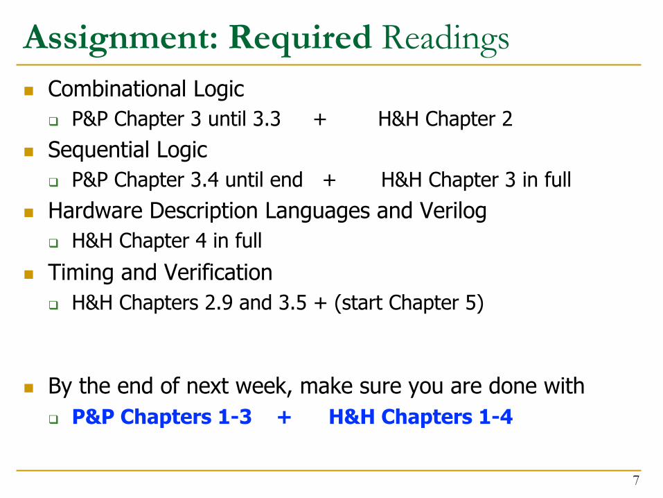
Assignment: Required Readingsn Combinational Logic
q P&P Chapter 3 until 3.3 + H&H Chapter 2n Sequential Logic
q P&P Chapter 3.4 until end + H&H Chapter 3 in fulln Hardware Description Languages and Verilog
q H&H Chapter 4 in fulln Timing and Verification
q H&H Chapters 2.9 and 3.5 + (start Chapter 5)
n By the end of next week, make sure you are done with q P&P Chapters 1-3 + H&H Chapters 1-4
7

Wrap-Up Combinational Logic Circuits and Design
8

Logic Simplification:Karnaugh Maps (K-Maps)
9

Recall: Logic Minimization Using K-Mapsn Very simple guideline:
q Circle all the rectangular blocks of 1’s in the map, using the fewest possible number of circlesn Each circle should be as large as possible
q Read off the implicants that were circled
n More formally:q A Boolean equation is minimized when it is written as a sum of
the fewest number of prime implicantsq Each circle on the K-map represents an implicantq The largest possible circles are prime implicants
10

Recall: K-map Rulesn What can be legally combined (circled) in the K-map?
q Rectangular groups of size 2k for any integer kq Each cell has the same value (1, for now)q All values must be adjacent
n Wrap-around edge is okay
n How does a group become a term in an expression?q Determine which literals are constant, and which vary across groupq Eliminate varying literals, then AND the constant literals
n constant 1 � use !, constant 0 � use "#
n What is a good solution?q Biggest groupings � eliminate more variables (literals) in each term q Fewest groupings � fewer terms (gates) all togetherq OR together all AND terms you create from individual groups
11
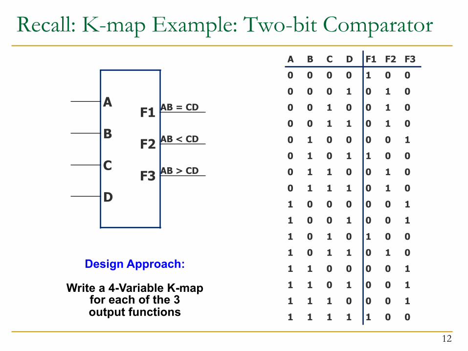
Recall: K-map Example: Two-bit Comparator
Design Approach:
Write a 4-Variable K-mapfor each of the 3output functions
12
A B C D F1 F2 F30 0 0 0 1 0 00 0 0 1 0 1 00 0 1 0 0 1 00 0 1 1 0 1 00 1 0 0 0 0 10 1 0 1 1 0 00 1 1 0 0 1 00 1 1 1 0 1 01 0 0 0 0 0 11 0 0 1 0 0 11 0 1 0 1 0 01 0 1 1 0 1 01 1 0 0 0 0 11 1 0 1 0 0 11 1 1 0 0 0 11 1 1 1 1 0 0
AF1 AB = CD
BF2 AB < CD
CF3 AB > CD
D
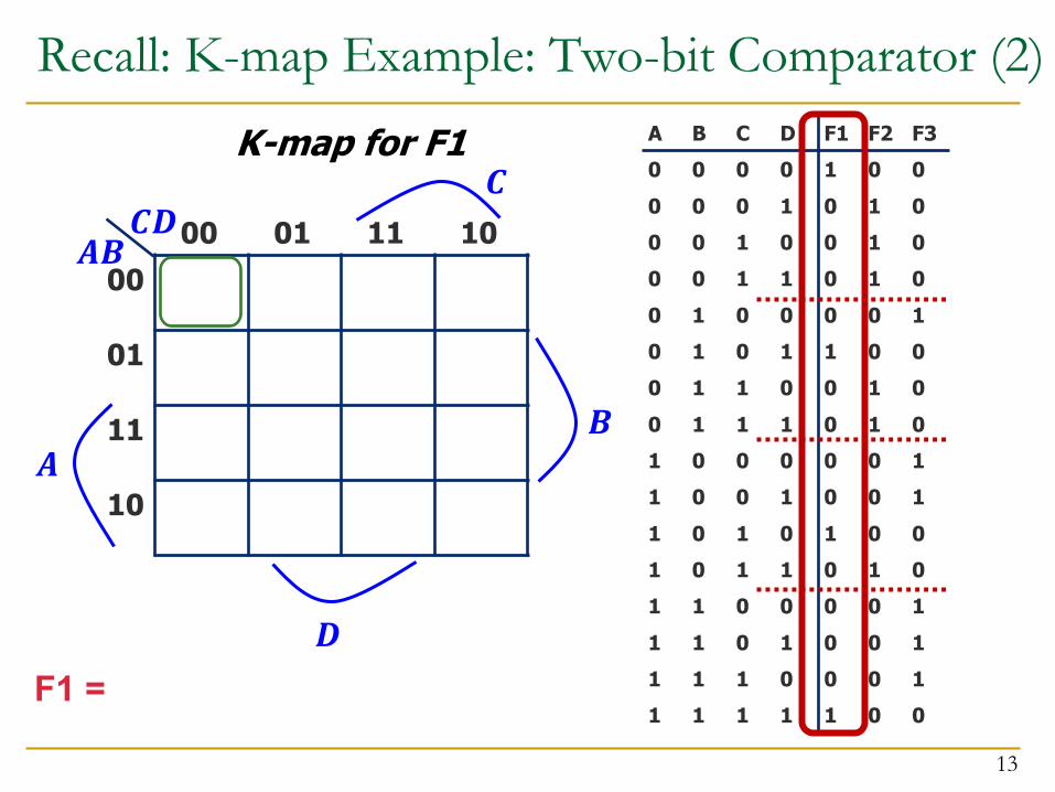
Recall: K-map Example: Two-bit Comparator (2)
13
A B C D F1 F2 F30 0 0 0 1 0 00 0 0 1 0 1 00 0 1 0 0 1 00 0 1 1 0 1 00 1 0 0 0 0 10 1 0 1 1 0 00 1 1 0 0 1 00 1 1 1 0 1 01 0 0 0 0 0 11 0 0 1 0 0 11 0 1 0 1 0 01 0 1 1 0 1 01 1 0 0 0 0 11 1 0 1 0 0 11 1 1 0 0 0 11 1 1 1 1 0 0
00 01 11 1000 101 111 110 1
K-map for F1
!"#$
F1 = A'B'C'D' + A'BC'D + ABCD + AB'CD'
!"
$
#
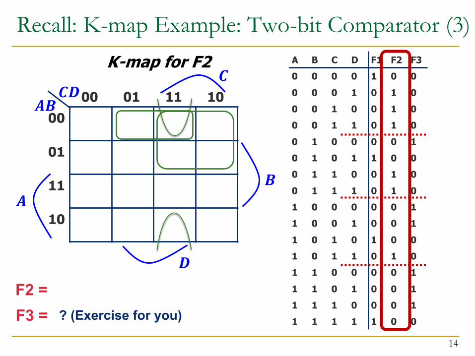
Recall: K-map Example: Two-bit Comparator (3)
14
A B C D F1 F2 F30 0 0 0 1 0 00 0 0 1 0 1 00 0 1 0 0 1 00 0 1 1 0 1 00 1 0 0 0 0 10 1 0 1 1 0 00 1 1 0 0 1 00 1 1 1 0 1 01 0 0 0 0 0 11 0 0 1 0 0 11 0 1 0 1 0 01 0 1 1 0 1 01 1 0 0 0 0 11 1 0 1 0 0 11 1 1 0 0 0 11 1 1 1 1 0 0
00 01 11 1000 1 1 101 1 111
10 1
K-map for F2
!"#$
F2 = A'C + A'B'D + B'CD
F3 = ? (Exercise for you)
!"
$
#
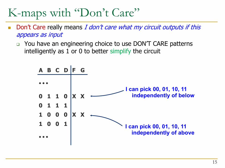
K-maps with “Don’t Care”n Don’t Care really means I don’t care what my circuit outputs if this
appears as inputq You have an engineering choice to use DON’T CARE patterns
intelligently as 1 or 0 to better simplify the circuit
15
I can pick 00, 01, 10, 11independently of below
I can pick 00, 01, 10, 11independently of above
A B C D F G
• • •
0 1 1 0 X X0 1 1 11 0 0 0 X X1 0 0 1
• • •

A B C D W X Y Z0 0 0 0 0 0 0 10 0 0 1 0 0 1 00 0 1 0 0 0 1 10 0 1 1 0 1 0 00 1 0 0 0 1 0 10 1 0 1 0 1 1 00 1 1 0 0 1 1 10 1 1 1 1 0 0 01 0 0 0 1 0 0 11 0 0 1 0 0 0 01 0 1 0 X X X X1 0 1 1 X X X X1 1 0 0 X X X X1 1 0 1 X X X X1 1 1 0 X X X X1 1 1 1 X X X X
Example: BCD Increment Functionn BCD (Binary Coded Decimal) digits
q Encode decimal digits 0 - 9 with bit patterns 00002 — 10012q When incremented, the decimal sequence is 0, 1, …, 8, 9, 0, 1
16
These input patterns shouldnever be encountered in practice
(hey -- it’s a BCD number!)So, associated output values are
“Don’t Cares”

00 01 11 1000 1 101 1 111 X X X X10 1 X X
K-map for BCD Increment Function
A B C D+ 1W X Y Z
17
00 01 11 100001 111 X X X X10 1 X X
00 01 11 1000 101 1 1 111 X X X X10 X X
00 01 11 1000 1 101 1 111 X X X X10 X X
W!"
#$ X!"
#$
!"#$!"
#$ ZY
Z (without don’t cares) = A'D' + B'C'D’
Z (with don’t cares) = D'
! "
$
#

K-map Summary
n Karnaugh maps as a formal systematic approachfor logic simplification
n 2-, 3-, 4-variable K-maps
n K-maps with “Don’t Care” outputs
n H&H Section 2.718

Sequential Logic Circuits and Design
19

What We Will Learn Todayn Circuits that can store information
q Cross-coupled inverterq R-S Latchq Gated D Latchq D Flip-Flopq Register
n Finite State Machines (FSM)q Moore Machineq Mealy Machine
n Verilog implementations of sequential circuits (next week)
20
Circuits that Can Store Information
21

Introductionn Combinational circuit output depends only on current inputn We want circuits that produce output depending on
current and past input values – circuits with memoryn How can we design a circuit that stores information?
22
Sequential Circuit
CombinationalCircuitin
puts
outputs
StorageElement

Capturing Data
23

Basic Element: Cross-Coupled Inverters
n Has two stable states: Q=1 or Q=0. n Has a third possible “metastable” state with both outputs
oscillating between 0 and 1 (we will see this later)n Not useful without a control mechanism for setting Q
24Image source: Harris and Harris, Digital Design and Computer Architecture, 2nd Ed., p.110.

More Realistic Storage Elementsn Have a control mechanism for setting Q
q We will see the R-S latch soonq Let’s look at an SRAM (static random access memory) cell first
n We will get back to SRAM (and DRAM) later
25
wordlinebitline bitline
SRAM cell

The Big Picture: Storage Elementsn Latches and Flip-Flops
q Very fast, parallel accessq Very expensive (one bit costs tens of transistors)
n Static RAM (SRAM)q Relatively fast, only one data word at a timeq Expensive (one bit costs 6+ transistors)
n Dynamic RAM (DRAM)q Slower, one data word at a time, reading destroys content
(refresh), needs special process for manufacturingq Cheap (one bit costs only one transistor plus one capacitor)
n Other storage technology (flash memory, hard disk, tape)q Much slower, access takes a long time, non-volatileq Very cheap (no transistors directly involved)

Basic Storage Element:The R-S Latch
27

The R-S (Reset-Set) Latchn Cross-coupled NAND gates
q Data is stored at Q (inverse at Q’)q S and R are control inputs
n In quiescent (idle) state, both S and R are held at 1n S (set): drive S to 0 (keeping R at 1) to change Q to 1n R (reset): drive R to 0 (keeping S at 1) to change Q to 0
n S and R should never both be 0 at the same time
28
S
R Q’
Q Input OutputR S Q1 1 Qprev
1 0 10 1 00 0 Forbidden

10
Why not R=S=0?
1. If R=S=0, Q and Q’ will both settle to 1, which breaksour invariant that Q = !Q’
2. If S and R transition back to 1 at the same time, Q and Q’begin to oscillate between 1 and 0 because their final values depend on each other (metastability)
q This eventually settles depending on variation in the circuits (more metastability to come in Lecture 8)
29
S
R Q’
Q Input OutputR S Q1 1 Qprev
1 0 10 1 00 0 Forbidden
10
0
01
1

The Gated D Latch
30

The Gated D Latchn How do we guarantee correct operation of an R-S Latch?
31
S
RQ’
Q

The Gated D Latchn How do we guarantee correct operation of an R-S Latch?
q Add two more NAND gates!
q Q takes the value of D, when write enable (WE) is set to 1 q S and R can never be 0 at the same time!
32
S
RQ’
Q
Write Enable
D
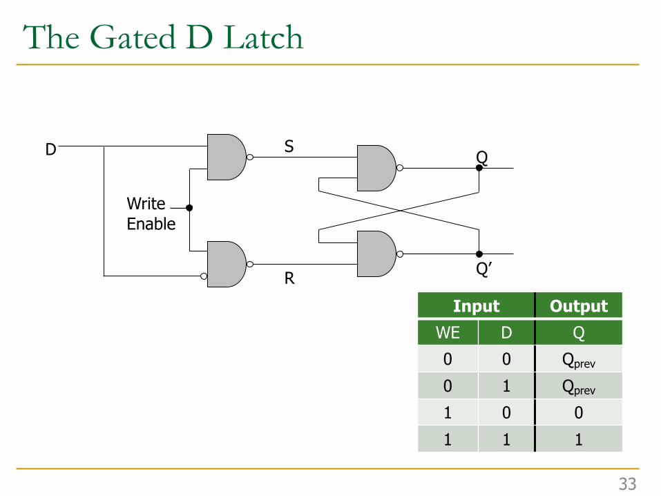
The Gated D Latch
33
S
R Q’
Q
Write Enable
D
Input OutputWE D Q0 0 Qprev
0 1 Qprev
1 0 01 1 1

The Register
34

The Register
35
D
Q
How can we use D latches to store more data?• Use more D latches!• A single WE signal for all latches forsimultaneous writes
D2
Q2
D1
Q1
D0
Q0
3
3
Write Enable
Here we have a register, or a structure that stores more than one bit and can be read from and written to
This register holds 4 bits, and its data is referenced as Q[3:0]

The Register
36
How can we use D latches to store more data?• Use more D latches!• A single WE signal for all latches forsimultaneous writes
Register x (Rx)
D3:0
Q3:0
WE
4
4
Here we have a register, or a structure that stores more than one bit and can be read from and written to
This register holds 4 bits, and its data is referenced as Q[3:0]

Memory
37
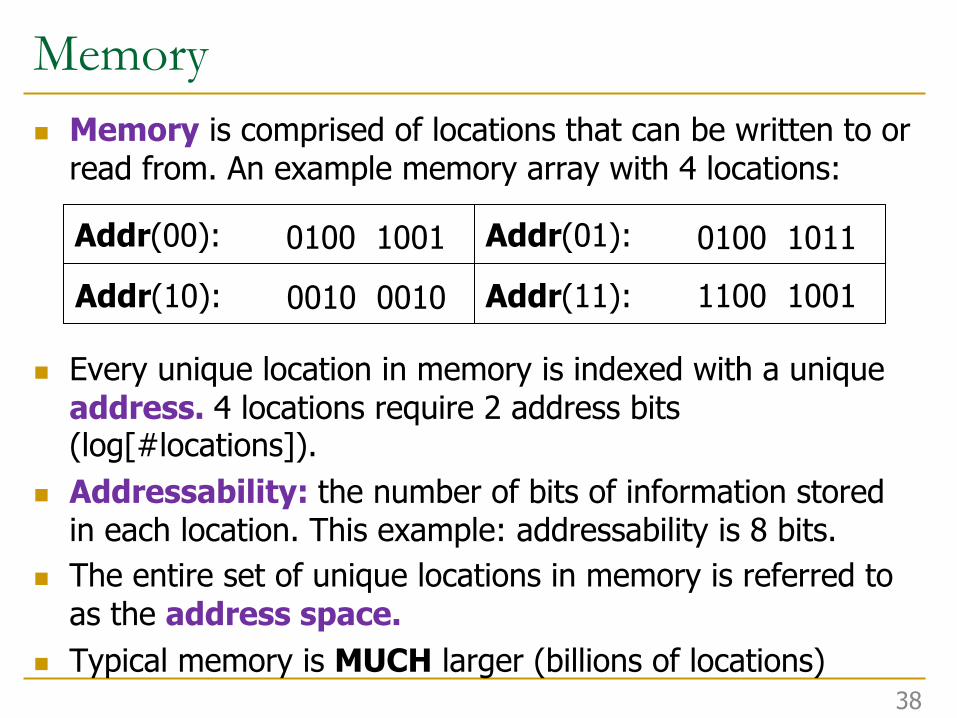
Memoryn Memory is comprised of locations that can be written to or
read from. An example memory array with 4 locations:
n Every unique location in memory is indexed with a unique address. 4 locations require 2 address bits (log[#locations]).
n Addressability: the number of bits of information stored in each location. This example: addressability is 8 bits.
n The entire set of unique locations in memory is referred to as the address space.
n Typical memory is MUCH larger (billions of locations)38
Addr(00):
Addr(10):
Addr(01):
Addr(11):
0100 1001
0010 0010
0100 1011
1100 1001
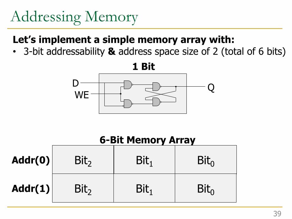
Addressing Memory
39
Let’s implement a simple memory array with: • 3-bit addressability & address space size of 2 (total of 6 bits)
D QWE
1 Bit
Bit2 Bit1 Bit0
Bit2 Bit1 Bit0
Addr(0)
Addr(1)
6-Bit Memory Array
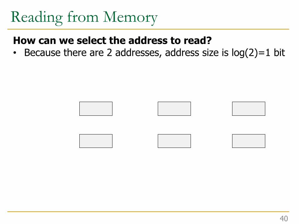
Reading from Memory
40
How can we select the address to read?• Because there are 2 addresses, address size is log(2)=1 bit

Reading from Memory
41
How can we select an address to read?• Because there are 2 addresses, address size is log(2)=1 bit
D[2] D[1] D[0]
Addr[0]
Wordline

Address Decoder
Reading from Memory
42
How can we select an address to read?• Because there are 2 addresses, address size is log(2)=1 bit
D[2] D[1] D[0]
Addr[0]
Wordline

Address Decoder
Reading from Memory
43
How can we select an address to read?• Because there are 2 addresses, address size is log(2)=1 bit
D[2] D[1] D[0]
Addr[0]
Multiplexer
Wordline

Writing to Memory
44
How can we select an address and write to it?
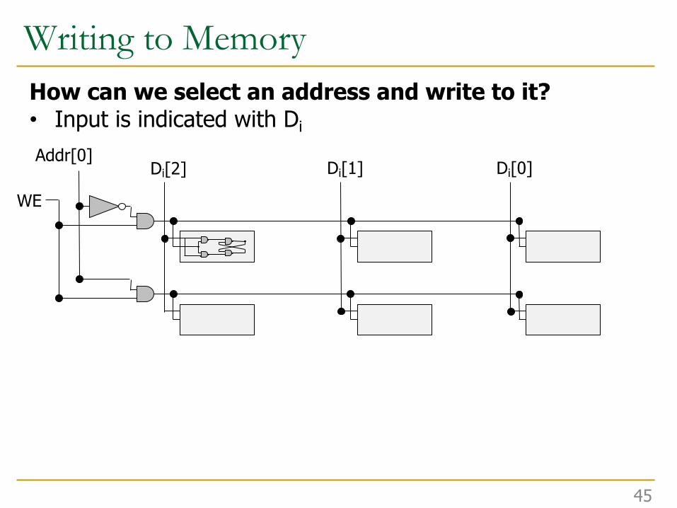
Writing to Memory
45
How can we select an address and write to it?• Input is indicated with Di
Di[2] Di[1] Di[0]Addr[0]
WE

Putting it all Together
46
Di[2] Di[1] Di[0]
D[2] D[1] D[0]
Addr[0]
WE
Let’s enable reading and writing to a memory array

A Bigger Memory Array
47
Di[2] Di[1] Di[0]
D[2] D[1] D[0]
Addr[1:0]
WE
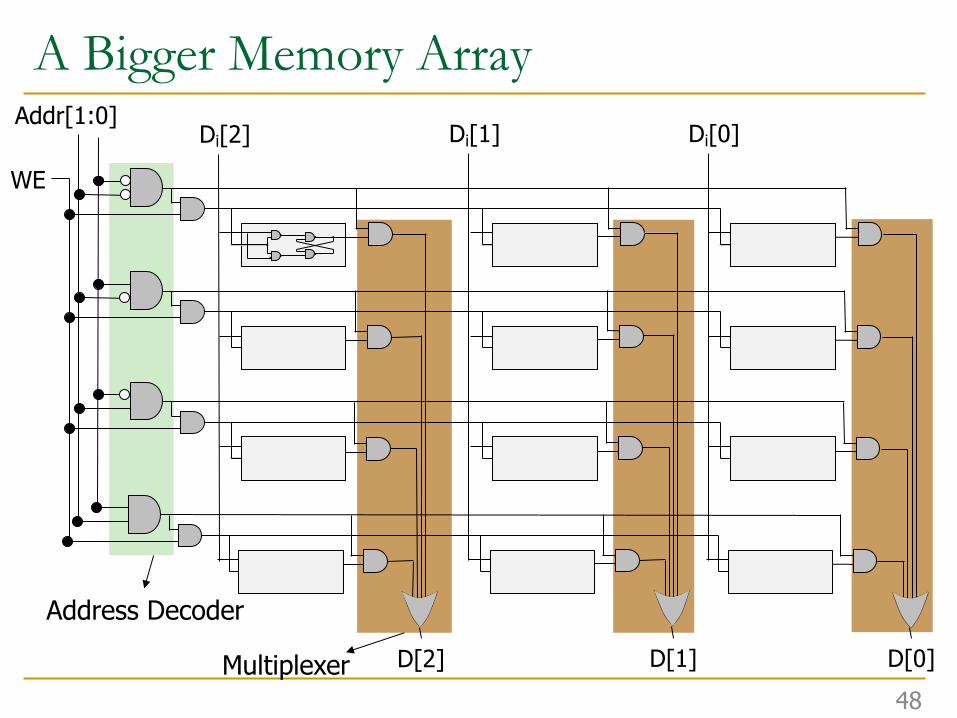
A Bigger Memory Array
48
Di[2] Di[1] Di[0]
D[2] D[1] D[0]
Addr[1:0]
WE
Address Decoder
Multiplexer

Sequential Logic Circuits
49

Sequential Logic Circuitsn We have looked at designs of circuit elements that can
store informationn Now, we will use these elements to build circuits that
remember past inputs
50https://www.easykeys.com/228_ESP_Combination_Lock.aspxhttps://www.fosmon.com/product/tsa-approved-lock-4-dial-combo
SequentialOpens depending on past inputs
CombinationalOnly depends on current inputs

Staten In order for this lock to work, it has to keep track
(remember) of the past events!n If passcode is R13-L22-R3, sequence of states to unlock:
A. The lock is not open (locked), and no relevant operations have been performed
B. Locked but user has completed R13C. Locked but user has completed R13-L22D. Unlocked: user has completed R13-L22-R3
n The state of a system is a snapshot of all relevant elements of the system at the moment of the snapshot
q To open the lock, states A-D must be completed in orderq If anything else happens (e.g., L5), lock returns to state A
51

State Diagram of Our Sequential Lockn Completely describes the operation of the sequential lock
n We will understand “state diagrams” fully later today52Image source: Patt and Patel, “Introduction to Computing Systems”, 2nd ed., page 76.

Another Simple Example of Staten A standard Swiss traffic light has 4 states
A. GreenB. YellowC. RedD. Red and Yellow
n The sequence of these states are always as follows
53
A B C D

Changing State: The Notion of Clock (I)
n When should the light change from one state to another?n We need a clock to dictate when to change state
q Clock signal alternates between 0 & 1
n At the start of a clock cycle ( ), system state changesq During a clock cycle, the state stays constantq In this traffic light example, we are assuming the traffic light stays in
each state an equal amount of time54
A B C D
CLK: 01

Changing State: The Notion of Clock (II)n Clock is a general mechanism that triggers transition from
one state to another in a sequential circuit
n Clock synchronizes state changes across many sequential circuit elements
n Combinational logic evaluates for the length of the clock cycle
n Clock cycle should be chosen to accommodate maximum combinational circuit delayq More on this later, when we discuss timing
55

Finite State Machines
56

Finite State Machinesn What is a Finite State Machine (FSM)?
q A discrete-time model of a stateful systemq Each state represents a snapshot of the system at a given time
n An FSM pictorially shows1. the set of all possible states that a system can be in 2. how the system transitions from one state to another
n An FSM can model q A traffic light, an elevator, fan speed, a microprocessor, etc.
n An FSM enables us to pictorially think of a statefulsystem using simple diagrams
57

Finite State Machines (FSMs) Consist of:n Five elements:
1. A finite number of states n State: snapshot of all relevant elements of the
system at the time of the snapshot2. A finite number of external inputs3. A finite number of external outputs4. An explicit specification of all state transitions
n How to get from one state to another5. An explicit specification of what determines
each external output value
58

Finite State Machines (FSMs)n Each FSM consists of three separate parts:
q next state logicq state registerq output logic
59
CLKM Nk knext
statelogic
outputlogic
inputs outputsstatenextstate
state register
At the beginning of the clock cycle, next state is latched into the state register

Finite State Machines (FSMs) Consist of:n Sequential circuits
q State register(s)n Store the current state and n Load the next state at the clock edge
n Combinational Circuitsq Next state logic
n Determines what the next state will be
q Output logicn Generates the outputs
60
NextState
CurrentState
S’ S
CLK
CL
Next StateLogic
NextState
CL
OutputLogic
Outputs

Finite State Machines (FSMs) Consist of:n Sequential circuits
q State register(s)n Store the current state and n Load the next state at the clock edge
n Combinational Circuitsq Next state logic
n Determines what the next state will be
q Output logicn Generates the outputs
61
NextState
CurrentState
S’ S
CLK
CL
Next StateLogic
NextState
CL
OutputLogic
Outputs

State Register Implementationn How can we implement a state register? Two properties:
1. We need to store data at the beginning of every clock cycle
2. The data must be available during the entire clock cycle
62
CLK: 01
RegisterInput:
RegisterOutput:
Desired behavior

The Problem with Latches
n Currently, we cannot simply wire a clock to WE of a latchq Whenever the clock is high, the latch propagates D to Qq The latch is transparent
63
D QCLK = WE
CLK: 01
RegisterInput:
RegisterOutput:
Recall the Gated D Latch

n Currently, we cannot simply wire a clock to WE of a latchq Whenever the clock is high, the latch propagates D to Qq The latch is transparent
The Problem with Latches
64
D QCLK = WE
CLK: 01
Register Input:
Register Output:
Recall the Gated D Latch
Undesirable!

n Currently, we cannot simply wire a clock to WE of a latchq When the clock is high Q will not take on D’s value ANDq When the clock is low the latch will propagate D to Q
The Problem with Latches
65
D QCLK = WE
CLK: 01
Input:
Output:
Recall the Gated D Latch
How can we change the latch, so that
1) D (input) is observable at Q (output) only at the beginning of next clock cycle?
2) Q is available for the full clock cycle

The Need for a New Storage Element n To design viable FSMs
n We need storage elements that allow us
q to read the current state throughout the current clock cycle
AND
q not write the next state values into the storage elements until the beginning of the next clock cycle.
66

n 1) state change on clock edge, 2) data available for full cycle
D Latch (Slave)D Latch (Master)
The D Flip-Flop
67
DQ
CLK
n When the clock is low, master propagates D to the input of slave (Q unchanged)n Only when the clock is high, slave latches D (Q stores D)
q At the rising edge of clock (clock going from 0->1), Q gets assigned D
CLK:01

The D Flip-Flopn 1) state change on clock edge, 2) data available for full cycle
68
n At the rising edge of clock (clock going from 0->1), Q gets assigned Dn At all other times, Q is unchanged
CLK:01
CLKD Q
Q__
D Flip-Flop

The D Flip-Flopn How do we implement this?
69
n At the rising edge of clock (clock going from 0->1), Q gets assigned Dn At all other times, Q is unchanged
CLK:01
CLKD Q
Q__
D Flip-FlopWe can use these Flip-Flops
to implement the state register!

Rising-Clock-Edge Triggered Flip-Flopn Two inputs: CLK, D
n Functionq The flip-flop “samples” D on the rising edgeof CLK (positive edge)
q When CLK rises from 0 to 1, D passes through to Qq Otherwise, Q holds its previous valueq Q changes only on the rising edge of CLK
n A flip-flop is called an edge-triggered state element because it captures data on the clock edgeq A latch is a level-triggered state element
70
D Flip-FlopSymbols
D QQ
CLK

Registern Multiple parallel flip-flops, each of which storing 1 bit
71
CLK
D Q
D Q
D Q
D Q
D0
D1
D2
D3
Q0
Q1
Q2
Q3
D3:04 4
CLK
Q3:0
This register stores 4 bits
This line represents 4 wires
Condensed

A 4-Bit D-Flip-Flop-Based Register (Internally)
72Image source: Patt and Patel, “Introduction to Computing Systems”, 3rd ed., tentative page 95.

Finite State Machines (FSMs)n Next state is determined by the current state and the inputsn Two types of finite state machines differ in the output
logic:q Moore FSM: outputs depend only on the current state
73
CLKM Nk knext
statelogic
outputlogic
Moore FSM
CLKM Nk knext
statelogic
outputlogic
inputs
inputs
outputs
outputsstate
statenextstate
nextstate
Mealy FSM

Finite State Machines (FSMs)n Next state is determined by the current state and the inputsn Two types of finite state machines differ in the output
logic:q Moore FSM: outputs depend only on the current stateq Mealy FSM: outputs depend on the current state and the
inputs
74
CLKM Nk knext
statelogic
outputlogic
Moore FSM
CLKM Nk knext
statelogic
outputlogic
inputs
inputs
outputs
outputsstate
statenextstate
nextstate
Mealy FSM

Finite State Machine Examplen “Smart” traffic light controller
q 2 inputs: n Traffic sensors: TA , TB (TRUE when there’s traffic)
q 2 outputs: n Lights: LA , LB (Red, Yellow, Green)
q State can change every 5 secondsn Except if green and traffic, stay green
75
TA
LA
TA
LB
TB
TB
LA
LB
Academic Ave.
BravadoBlvd.
Dorms
Fields
DiningHall
Labs
From H&H Section 3.4.1

Finite State Machine Black Boxn Inputs: CLK, Reset, TA , TBn Outputs: LA , LB
76
TA
TB
LA
LB
CLK
Reset
TrafficLight
Controller

Finite State Machine Transition Diagramn Moore FSM: outputs labeled in each state
q States: Circlesq Transitions: Arcs
77
S0LA: greenLB: red
Reset
TA
LA
TA
LB
TB
TB
LA
LB
Academic Ave.
BravadoBlvd.
Dorms
Fields
DiningHall
Labs

Finite State Machine Transition Diagramn Moore FSM: outputs labeled in each state
q States: Circlesq Transitions: Arcs
78
TA
LA
TA
LB
TB
TB
LA
LB
Academic Ave.
BravadoBlvd.
Dorms
Fields
DiningHall
Labs
S0LA: greenLB: red
S1LA: yellowLB: red
S3LA: redLB: yellow
S2LA: redLB: green
TATA
TB
TB
Reset

Finite State Machine Transition Diagramn Moore FSM: outputs labeled in each state
q States: Circlesq Transitions: Arcs
79
TA
LA
TA
LB
TB
TB
LA
LB
Academic Ave.
BravadoBlvd.
Dorms
Fields
DiningHall
Labs
S0LA: greenLB: red
S1LA: yellowLB: red
S3LA: redLB: yellow
S2LA: redLB: green
TATA
TB
TB
Reset

Finite State Machine Transition Diagramn Moore FSM: outputs labeled in each state
q States: Circlesq Transitions: Arcs
80
TA
LA
TA
LB
TB
TB
LA
LB
Academic Ave.
BravadoBlvd.
Dorms
Fields
DiningHall
Labs
S0LA: greenLB: red
S1LA: yellowLB: red
S3LA: redLB: yellow
S2LA: redLB: green
TATA
TB
TB
Reset

Finite State Machine Transition Diagramn Moore FSM: outputs labeled in each state
q States: Circlesq Transitions: Arcs
81
TA
LA
TA
LB
TB
TB
LA
LB
Academic Ave.
BravadoBlvd.
Dorms
Fields
DiningHall
Labs
S0LA: greenLB: red
S1LA: yellowLB: red
S3LA: redLB: yellow
S2LA: redLB: green
TATA
TB
TB
Reset

Finite State Machine:State Transition Table
82

FSM State Transition TableCurrentState Inputs NextState
S TA TB S'S0 0 XS0 1 XS1 X XS2 X 0S2 X 1S3 X X
S0LA: greenLB: red
S1LA: yellowLB: red
S3LA: redLB: yellow
S2LA: redLB: green
TATA
TB
TB
Reset
59

FSM State Transition TableCurrentState Inputs NextState
S TA TB S'S0 0 X S1S0 1 X S0S1 X X S2S2 X 0 S3S2 X 1 S2S3 X X S0
S0LA: greenLB: red
S1LA: yellowLB: red
S3LA: redLB: yellow
S2LA: redLB: green
TATA
TB
TB
Reset
60

FSM State Transition TableCurrentState Inputs NextState
S TA TB S'S0 0 X S1S0 1 X S0S1 X X S2S2 X 0 S3S2 X 1 S2S3 X X S0
S0LA: greenLB: red
S1LA: yellowLB: red
S3LA: redLB: yellow
S2LA: redLB: green
TATA
TB
TB
Reset
State Encoding
S0 00S1 01S2 10S3 11
61

FSM State Transition TableCurrentState Inputs NextStateS1 S0 TA TB S’1 S’00 0 0 X 0 10 0 1 X 0 00 1 X X 1 01 0 X 0 1 11 0 X 1 1 01 1 X X 0 0
S0LA: greenLB: red
S1LA: yellowLB: red
S3LA: redLB: yellow
S2LA: redLB: green
TATA
TB
TB
Reset
State Encoding
S0 00S1 01S2 10S3 11
62

FSM State Transition TableCurrentState Inputs NextStateS1 S0 TA TB S’1 S’00 0 0 X 0 10 0 1 X 0 00 1 X X 1 01 0 X 0 1 11 0 X 1 1 01 1 X X 0 0
S0LA: greenLB: red
S1LA: yellowLB: red
S3LA: redLB: yellow
S2LA: redLB: green
TATA
TB
TB
Reset
State Encoding
S0 00S1 01S2 10S3 11
S’1 =?
63

FSM State Transition TableCurrentState Inputs NextStateS1 S0 TA TB S’1 S’00 0 0 X 0 10 0 1 X 0 00 1 X X 1 01 0 X 0 1 11 0 X 1 1 01 1 X X 0 0
S0LA: greenLB: red
S1LA: yellowLB: red
S3LA: redLB: yellow
S2LA: redLB: green
TATA
TB
TB
Reset
State Encoding
S0 00S1 01S2 10S3 11
S’1 =(S1 ∙S0)+(S1 ∙S0 ∙TB)+(S1 ∙S0 ∙TB)
64

FSM State Transition TableCurrentState Inputs NextStateS1 S0 TA TB S’1 S’00 0 0 X 0 10 0 1 X 0 00 1 X X 1 01 0 X 0 1 11 0 X 1 1 01 1 X X 0 0
S0LA: greenLB: red
S1LA: yellowLB: red
S3LA: redLB: yellow
S2LA: redLB: green
TATA
TB
TB
Reset
State Encoding
S0 00S1 01S2 10S3 11
S’1 =(S1 ∙S0)+(S1 ∙S0 ∙TB)+(S1 ∙S0 ∙TB)
S’0 =?65
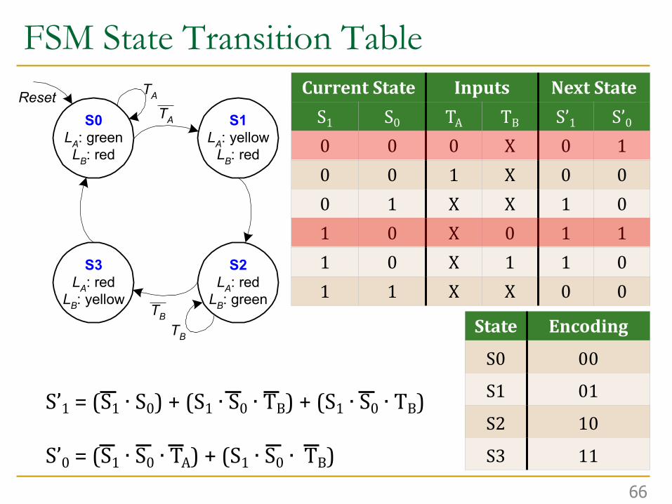
FSM State Transition TableCurrentState Inputs NextStateS1 S0 TA TB S’1 S’00 0 0 X 0 10 0 1 X 0 00 1 X X 1 01 0 X 0 1 11 0 X 1 1 01 1 X X 0 0
S0LA: greenLB: red
S1LA: yellowLB: red
S3LA: redLB: yellow
S2LA: redLB: green
TATA
TB
TB
Reset
State Encoding
S0 00S1 01S2 10S3 11
S’1 =(S1 ∙S0)+(S1 ∙S0 ∙TB)+(S1 ∙S0 ∙TB)
S’0 =(S1 ∙S0 ∙TA)+(S1 ∙S0 ∙TB)66

FSM State Transition TableCurrentState Inputs NextStateS1 S0 TA TB S’1 S’00 0 0 X 0 10 0 1 X 0 00 1 X X 1 01 0 X 0 1 11 0 X 1 1 01 1 X X 0 0
S0LA: greenLB: red
S1LA: yellowLB: red
S3LA: redLB: yellow
S2LA: redLB: green
TATA
TB
TB
Reset
State Encoding
S0 00S1 01S2 10S3 11
S’1 =S1 xor S0(Simplified)
S’0 =(S1 ∙S0 ∙TA)+(S1 ∙S0 ∙TB)67

Finite State Machine:Output Table
92

FSM Output Table
S0LA: greenLB: red
S1LA: yellowLB: red
S3LA: redLB: yellow
S2LA: redLB: green
TATA
TB
TB
Reset CurrentState OutputsS1 S0 LA LB0 0 green red0 1 yellow red1 0 red green1 1 red yellow
69

FSM Output Table
S0LA: greenLB: red
S1LA: yellowLB: red
S3LA: redLB: yellow
S2LA: redLB: green
TATA
TB
TB
Reset CurrentState OutputsS1 S0 LA LB0 0 green red0 1 yellow red1 0 red green1 1 red yellow
Output Encoding
green 00yellow 01red 10
70
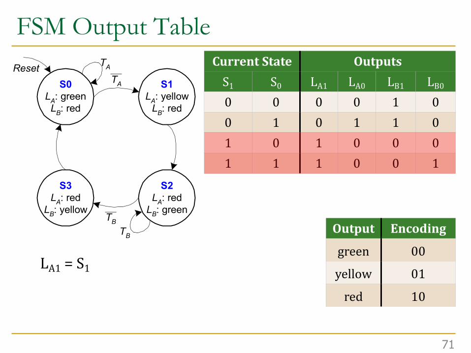
FSM Output Table
S0LA: greenLB: red
S1LA: yellowLB: red
S3LA: redLB: yellow
S2LA: redLB: green
TATA
TB
TB
Reset CurrentState OutputsS1 S0 LA1 LA0 LB1 LB00 0 0 0 1 00 1 0 1 1 01 0 1 0 0 01 1 1 0 0 1
Output Encoding
green 00yellow 01red 10
LA1 =S1
71

FSM Output Table
S0LA: greenLB: red
S1LA: yellowLB: red
S3LA: redLB: yellow
S2LA: redLB: green
TATA
TB
TB
Reset CurrentState OutputsS1 S0 LA1 LA0 LB1 LB00 0 0 0 1 00 1 0 1 1 01 0 1 0 0 01 1 1 0 0 1
Output Encoding
green 00yellow 01red 10
LA1 =S1LA0 =S1 ∙S0
72

FSM Output Table
S0LA: greenLB: red
S1LA: yellowLB: red
S3LA: redLB: yellow
S2LA: redLB: green
TATA
TB
TB
Reset CurrentState OutputsS1 S0 LA1 LA0 LB1 LB00 0 0 0 1 00 1 0 1 1 01 0 1 0 0 01 1 1 0 0 1
Output Encoding
green 00yellow 01red 10
LA1 =S1LA0 =S1 ∙S0LB1 =S1
73

FSM Output Table
S0LA: greenLB: red
S1LA: yellowLB: red
S3LA: redLB: yellow
S2LA: redLB: green
TATA
TB
TB
Reset CurrentState OutputsS1 S0 LA1 LA0 LB1 LB00 0 0 0 1 00 1 0 1 1 01 0 1 0 0 01 1 1 0 0 1
Output Encoding
green 00yellow 01red 10
LA1 =S1LA0 =S1 ∙S0LB1 =S1LB0 =S1 ∙S0
74
Finite State Machine:Schematic
99
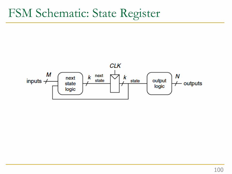
FSM Schematic: State Register
100

101
FSM Schematic: State Register
S1
S0
S'1
S'0
CLK
state register
Resetr
102
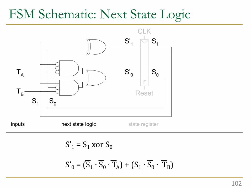
FSM Schematic: Next State Logic
S1
S0
S'1
S'0
CLK
next state logic state register
Reset
TA
TB
inputs
S1 S0
r
S’1 =S1 xor S0
S’0 =(S1 ∙S0 ∙TA)+(S1 ∙S0 ∙TB)

103
FSM Schematic: Output Logic
S1
S0
S'1
S'0
CLK
next state logic output logicstate register
Reset
LA1
LB1
LB0
LA0
TA
TB
inputs outputs
S1 S0
r
LA1 =S1LA0 =S1 ∙S0LB1 =S1LB0 =S1 ∙S0

104
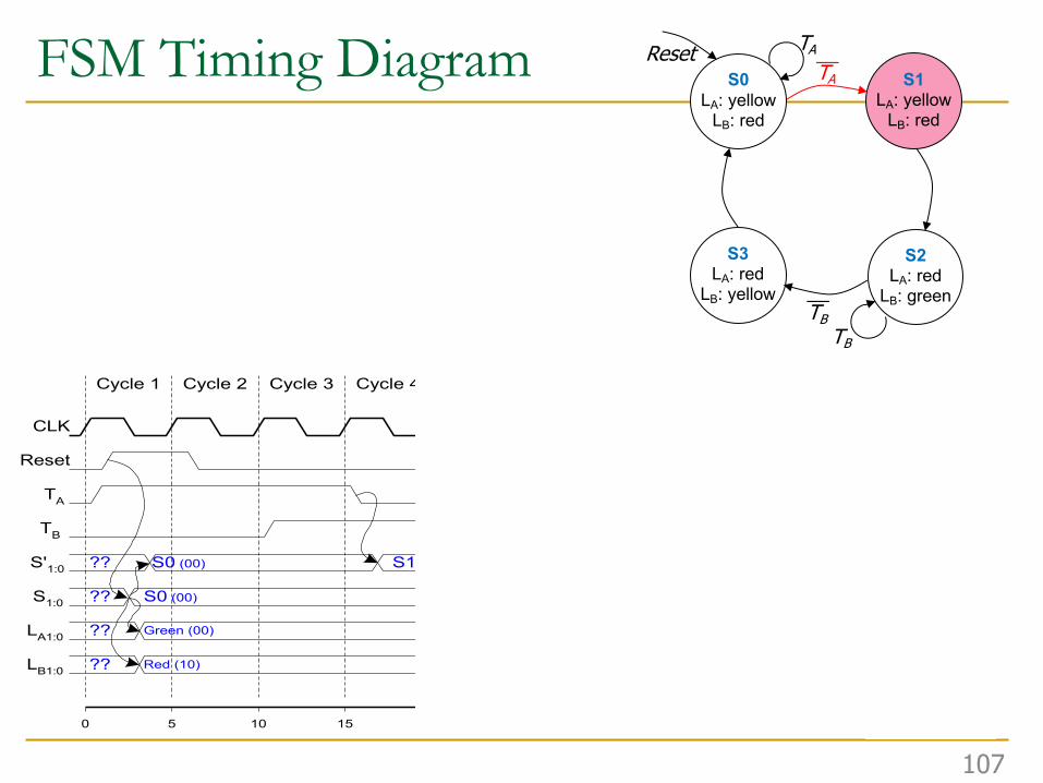
FSM Timing Diagram
CLK
Reset
TA
TB
S'1:0
S1:0
LA1:0
LB1:0
Cycle 1 Cycle 2 Cycle 3 Cycle 4 Cycle 5 Cycle 6 Cycle 7 Cycle 8 Cycle 9 Cycle 10
S1 (01) S2 (10) S3 (11) S0 (00)
t (sec)
??
??
S0 (00)
S0 (00) S1 (01) S2 (10) S3 (11) S1 (01)
??
??
0 5 10 15 20 25 30 35 40 45
Green (00)
Red (10)
S0 (00)
Yellow (01) Red (10) Green (00)
Green (00) Red (10)Yellow (01)
S0LA: yellow
LB: red
S1LA: yellow
LB: red
S2LA: red
LB: green
S3LA: red
LB: yellow
Reset TATA__
__TBTB

105
FSM Timing Diagram
CLK
Reset
TA
TB
S'1:0
S1:0
LA1:0
LB1:0
Cycle 1 Cycle 2 Cycle 3 Cycle 4 Cycle 5 Cycle 6 Cycle 7 Cycle 8 Cycle 9 Cycle 10
S1 (01) S2 (10) S3 (11) S0 (00)
t (sec)
??
??
S0 (00)
S0 (00) S1 (01) S2 (10) S3 (11) S1 (01)
??
??
0 5 10 15 20 25 30 35 40 45
Green (00)
Red (10)
S0 (00)
Yellow (01) Red (10) Green (00)
Green (00) Red (10)Yellow (01)
S0LA: yellow
LB: red
S1LA: yellow
LB: red
S2LA: red
LB: green
S3LA: red
LB: yellow
Reset TATA__
__TBTB

106
FSM Timing Diagram
CLK
Reset
TA
TB
S'1:0
S1:0
LA1:0
LB1:0
Cycle 1 Cycle 2 Cycle 3 Cycle 4 Cycle 5 Cycle 6 Cycle 7 Cycle 8 Cycle 9 Cycle 10
S1 (01) S2 (10) S3 (11) S0 (00)
t (sec)
??
??
S0 (00)
S0 (00) S1 (01) S2 (10) S3 (11) S1 (01)
??
??
0 5 10 15 20 25 30 35 40 45
Green (00)
Red (10)
S0 (00)
Yellow (01) Red (10) Green (00)
Green (00) Red (10)Yellow (01)
S0LA: yellow
LB: red
S1LA: yellow
LB: red
S2LA: red
LB: green
S3LA: red
LB: yellow
Reset TATA__
__TBTB
107
FSM Timing Diagram
CLK
Reset
TA
TB
S'1:0
S1:0
LA1:0
LB1:0
Cycle 1 Cycle 2 Cycle 3 Cycle 4 Cycle 5 Cycle 6 Cycle 7 Cycle 8 Cycle 9 Cycle 10
S1 (01) S2 (10) S3 (11) S0 (00)
t (sec)
??
??
S0 (00)
S0 (00) S1 (01) S2 (10) S3 (11) S1 (01)
??
??
0 5 10 15 20 25 30 35 40 45
Green (00)
Red (10)
S0 (00)
Yellow (01) Red (10) Green (00)
Green (00) Red (10)Yellow (01)
S0LA: yellow
LB: red
S1LA: yellow
LB: red
S2LA: red
LB: green
S3LA: red
LB: yellow
Reset TATA__
__TBTB

108
FSM Timing Diagram
CLK
Reset
TA
TB
S'1:0
S1:0
LA1:0
LB1:0
Cycle 1 Cycle 2 Cycle 3 Cycle 4 Cycle 5 Cycle 6 Cycle 7 Cycle 8 Cycle 9 Cycle 10
S1 (01) S2 (10) S3 (11) S0 (00)
t (sec)
??
??
S0 (00)
S0 (00) S1 (01) S2 (10) S3 (11) S1 (01)
??
??
0 5 10 15 20 25 30 35 40 45
Green (00)
Red (10)
S0 (00)
Yellow (01) Red (10) Green (00)
Green (00) Red (10)Yellow (01)
S0LA: yellow
LB: red
S1LA: yellow
LB: red
S2LA: red
LB: green
S3LA: red
LB: yellow
Reset TATA__
__TBTB

109
FSM Timing Diagram
CLK
Reset
TA
TB
S'1:0
S1:0
LA1:0
LB1:0
Cycle 1 Cycle 2 Cycle 3 Cycle 4 Cycle 5 Cycle 6 Cycle 7 Cycle 8 Cycle 9 Cycle 10
S1 (01) S2 (10) S3 (11) S0 (00)
t (sec)
??
??
S0 (00)
S0 (00) S1 (01) S2 (10) S3 (11) S1 (01)
??
??
0 5 10 15 20 25 30 35 40 45
Green (00)
Red (10)
S0 (00)
Yellow (01) Red (10) Green (00)
Green (00) Red (10)Yellow (01)
S0LA: yellow
LB: red
S1LA: yellow
LB: red
S2LA: red
LB: green
S3LA: red
LB: yellow
Reset TATA__
__TBTB
110
FSM Timing Diagram
CLK
Reset
TA
TB
S'1:0
S1:0
LA1:0
LB1:0
Cycle 1 Cycle 2 Cycle 3 Cycle 4 Cycle 5 Cycle 6 Cycle 7 Cycle 8 Cycle 9 Cycle 10
S1 (01) S2 (10) S3 (11) S0 (00)
t (sec)
??
??
S0 (00)
S0 (00) S1 (01) S2 (10) S3 (11) S1 (01)
??
??
0 5 10 15 20 25 30 35 40 45
Green (00)
Red (10)
S0 (00)
Yellow (01) Red (10) Green (00)
Green (00) Red (10)Yellow (01)
S0LA: yellow
LB: red
S1LA: yellow
LB: red
S2LA: red
LB: green
S3LA: red
LB: yellow
Reset TATA__
__TBTB

111
FSM Timing Diagram
CLK
Reset
TA
TB
S'1:0
S1:0
LA1:0
LB1:0
Cycle 1 Cycle 2 Cycle 3 Cycle 4 Cycle 5 Cycle 6 Cycle 7 Cycle 8 Cycle 9 Cycle 10
S1 (01) S2 (10) S3 (11) S0 (00)
t (sec)
??
??
S0 (00)
S0 (00) S1 (01) S2 (10) S3 (11) S1 (01)
??
??
0 5 10 15 20 25 30 35 40 45
Green (00)
Red (10)
S0 (00)
Yellow (01) Red (10) Green (00)
Green (00) Red (10)Yellow (01)
S0LA: yellow
LB: red
S1LA: yellow
LB: red
S2LA: red
LB: green
S3LA: red
LB: yellow
Reset TATA__
__TBTBThis is from H&H Section 3.4.1
112
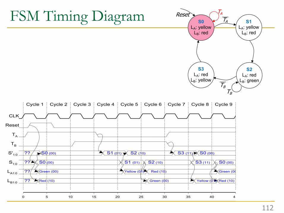
FSM Timing Diagram
CLK
Reset
TA
TB
S'1:0
S1:0
LA1:0
LB1:0
Cycle 1 Cycle 2 Cycle 3 Cycle 4 Cycle 5 Cycle 6 Cycle 7 Cycle 8 Cycle 9 Cycle 10
S1 (01) S2 (10) S3 (11) S0 (00)
t (sec)
??
??
S0 (00)
S0 (00) S1 (01) S2 (10) S3 (11) S1 (01)
??
??
0 5 10 15 20 25 30 35 40 45
Green (00)
Red (10)
S0 (00)
Yellow (01) Red (10) Green (00)
Green (00) Red (10)Yellow (01)
S0LA: yellow
LB: red
S1LA: yellow
LB: red
S2LA: red
LB: green
S3LA: red
LB: yellow
Reset TATA__
__TBTB

113
FSM Timing Diagram
CLK
Reset
TA
TB
S'1:0
S1:0
LA1:0
LB1:0
Cycle 1 Cycle 2 Cycle 3 Cycle 4 Cycle 5 Cycle 6 Cycle 7 Cycle 8 Cycle 9 Cycle 10
S1 (01) S2 (10) S3 (11) S0 (00)
t (sec)
??
??
S0 (00)
S0 (00) S1 (01) S2 (10) S3 (11) S1 (01)
??
??
0 5 10 15 20 25 30 35 40 45
Green (00)
Red (10)
S0 (00)
Yellow (01) Red (10) Green (00)
Green (00) Red (10)Yellow (01)
S0LA: yellow
LB: red
S1LA: yellow
LB: red
S2LA: red
LB: green
S3LA: red
LB: yellow
Reset TATA__
__TBTB

Design of Digital CircuitsLecture 6: Sequential Logic Design
Prof. Onur MutluETH ZurichSpring 2019
8 March 2019

We did not cover the remaining slides. They are for your preparation for the
next lecture.
115

FSM State Encodingn How do we encode the state bits?
q Three common state binary encodings with different tradeoffs1. Fully Encoded2. 1-Hot Encoded3. Output Encoded
n Let’s see an example Swiss traffic light with 4 statesq Green, Yellow, Red, Yellow+Red
116

FSM State Encoding1. Fully Encoded:
q Minimizes # flip-flops, but not necessarily output logic or next state logic
q Use log2(num_states) bits to represent the statesq Example states: 00, 01, 10, 11
2. 1-Hot Encoded:q Maximizes # flip-flops, minimizes next state logicq Simplest design process – very automatableq Use num_states bits to represent the statesq Example states: 0001, 0010, 0100, 1000
117
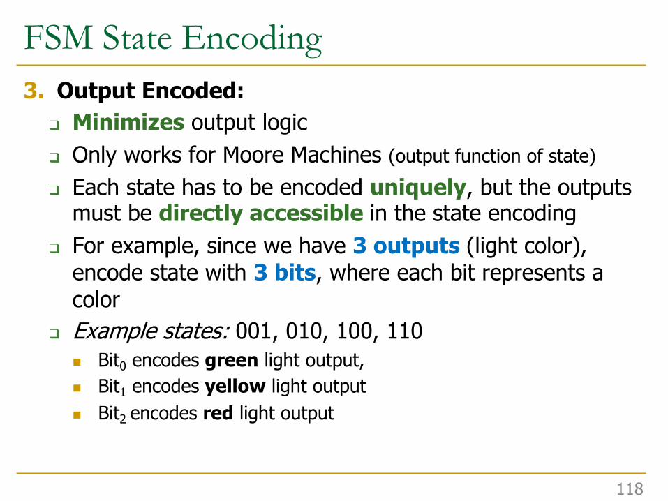
FSM State Encoding3. Output Encoded:
q Minimizes output logic q Only works for Moore Machines (output function of state)q Each state has to be encoded uniquely, but the outputs
must be directly accessible in the state encodingq For example, since we have 3 outputs (light color),
encode state with 3 bits, where each bit represents a color
q Example states: 001, 010, 100, 110n Bit0 encodes green light output, n Bit1 encodes yellow light outputn Bit2 encodes red light output
118

FSM State Encoding3. Output Encoded:
q Minimizes output logic q Only works for Moore Machines (output function of state)q Each state has to be encoded uniquely, but the outputs
must be directly accessible in the state encodingq For example, since we have 3 outputs (light color),
encode state with 3 bits, where each bit represents a color
q Example states: 001, 010, 100, 110n Bit0 encodes green light output, n Bit1 encodes yellow light outputn Bit2 encodes red light output
119
The designer must carefully choosean encoding scheme to optimize the design
under given constraints

Moore vs. Mealy Machines
120
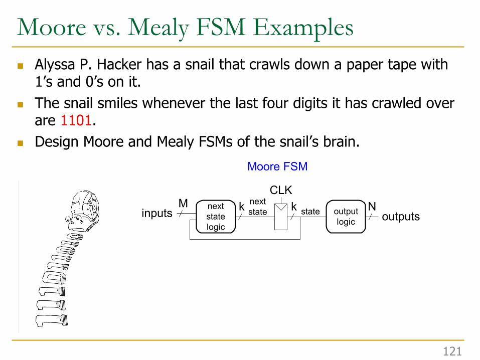
Moore vs. Mealy FSM Examplesn Alyssa P. Hacker has a snail that crawls down a paper tape with
1’s and 0’s on it. n The snail smiles whenever the last four digits it has crawled over
are 1101. n Design Moore and Mealy FSMs of the snail’s brain.
121
CLKM Nk knext
statelogic
outputlogic
Moore FSM
CLKM Nk knext
statelogic
outputlogic
inputs
inputs
outputs
outputsstate
statenextstate
nextstate
Mealy FSM

Moore vs. Mealy FSM Examplesn Alyssa P. Hacker has a snail that crawls down a paper tape with
1’s and 0’s on it. n The snail smiles whenever the last four digits it has crawled over
are 1101. n Design Moore and Mealy FSMs of the snail’s brain.
122
CLKM Nk knext
statelogic
outputlogic
Moore FSM
CLKM Nk knext
statelogic
outputlogic
inputs
inputs
outputs
outputsstate
statenextstate
nextstate
Mealy FSM

State Transition Diagrams
123
reset
Moore FSM
S00
S10
S20
S30
S41
0
1 1 0 1
1
01 00
reset
S0 S1 S2 S30/0
1/0 1/0 0/01/1
0/01/0
0/0
Mealy FSMWhat are the tradeoffs?

FSM Design Proceduren Determine all possible states of your machinen Develop a state transition diagram
q Generally this is done from a textual descriptionq You need to 1) determine the inputs and outputs for each state and
2) figure out how to get from one state to anothern Approach
q Start by defining the reset state and what happens from it – this is typically an easy point to start from
q Then continue to add transitions and statesq Picking good state names is very importantq Building an FSM is like programming (but it is not programming!)
n An FSM has a sequential “control-flow” like a program with conditionals and goto’sn The if-then-else construct is controlled by one or more inputsn The outputs are controlled by the state or the inputs
q In hardware, we typically have many concurrent FSMs
124

What is to Come: LC-3 Processor
125
Scanned by CamScanner

What is to Come: LC-3 Datapath
126

Backup Slides:Different Types of Flip Flops
127

The D Flip-Flop
128

Enabled Flip-Flopsn Inputs: CLK, D, EN
q The enable input (EN) controls when new data (D) is storedn Function:
q EN = 1: D passes through to Q on the clock edge q EN = 0: the flip-flop retains its previous state
129
InternalCircuit
D Q
CLKEN
DQ
0
1D QEN
Symbol

Resettable Flip-Flopn Inputs: CLK, D, Reset
q The Reset is used to set the output to 0.n Function:
q Reset = 1: Q is forced to 0 q Reset = 0: the flip-flop behaves like an ordinary D flip-flop
130
Symbols
D QReset
r

Resettable Flip-Flopsn Two types:
q Synchronous: resets at the clock edge onlyq Asynchronous: resets immediately when Reset = 1
n Asynchronously resettable flip-flop requires changing the internal circuitry of the flip-flop (see Exercise 3.10)
n Synchronously resettable flip-flop?
131
InternalCircuit
D Q
CLK
D QReset

Settable Flip-Flopn Inputs: CLK, D, Setn Function:
q Set = 1: Q is set to 1 q Set = 0: the flip-flop behaves like an ordinary D flip-flop
132
Symbols
D QSet
s

Recall:Combinational Logic Blocks
133

Recall: Combinational Building Blocksn Combinational logic is often grouped into larger building
blocks to build more complex systems
n Hides the unnecessary gate-level details to emphasize the function of the building block
n We now look at: q Decodersq Multiplexersq Full adderq PLA (Programmable Logic Array)

Recall: Decodern n inputs and 2n outputsn Exactly one of the outputs is 1 and all the rest are 0sn The one output that is logically 1 is the output
corresponding to the input pattern that the logic circuit is expected to detectA 1 if A,B is 00B
1 if A,B is 01
1 if A,B is 10
1 if A,B is 11
A = 1 0B = 0
0
1
0

Recall: Multiplexer (MUX), or Selectorn Selects one of the N inputs to connect it to the outputn Needs log2N-bit control inputn 2:1 MUX A B
S
C
ba
A B
S = 0
C
0A
A
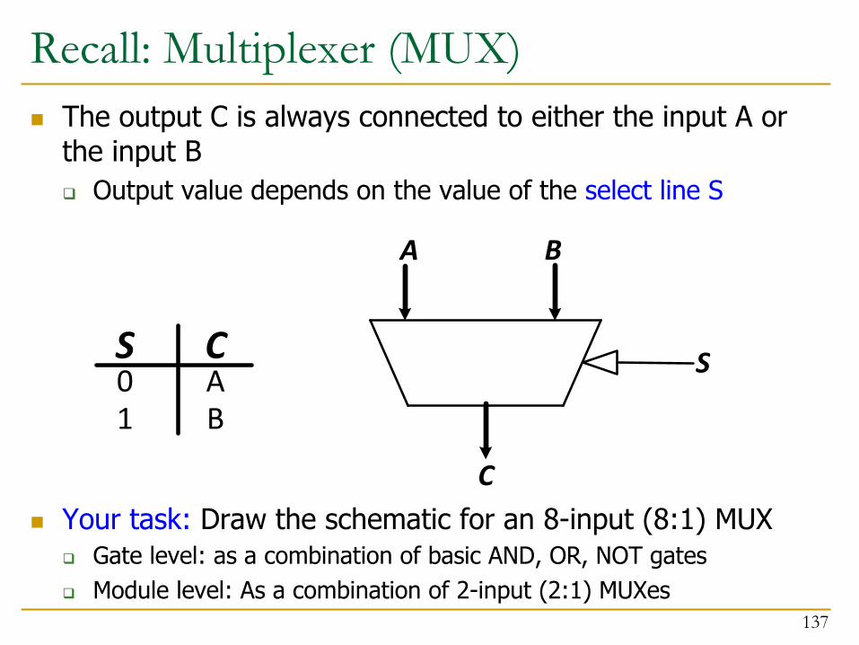
Recall: Multiplexer (MUX)n The output C is always connected to either the input A or
the input Bq Output value depends on the value of the select line S
n Your task: Draw the schematic for an 8-input (8:1) MUXq Gate level: as a combination of basic AND, OR, NOT gatesq Module level: As a combination of 2-input (2:1) MUXes
137
A B
S
C
S C0 A1 B