design of high speed low voltage data converters for …
TRANSCRIPT

DESIGN OF HIGH SPEED LOW VOLTAGE
DATA CONVERTERS FOR UWB COMMUNICATION SYSTEMS
A Thesis
by
CHOONG HOON LEE
Submitted to the Office of Graduate Studies of Texas A&M University
in partial fulfillment of the requirements for the degree of
MASTER OF SCIENCE
May 2006
Major Subject: Electrical Engineering

DESIGN OF HIGH SPEED LOW VOLTAGE
DATA CONVERTERS FOR UWB COMMUNICATION SYSTEMS
A Thesis
by
CHOONG HOON LEE
Submitted to the Office of Graduate Studies of Texas A&M University
in partial fulfillment of the requirements for the degree of
MASTER OF SCIENCE
Approved by: Chair of Committee, Aydin Karsilayan Committee Members, Jose Silva-Martinez Scott Miller Chii-Der S.Suh Head of Department, Scott Miller
May 2006
Major Subject: Electrical Engineering

iii
ABSTRACT
Design of High Speed Low Voltage
Data Converters for UWB Communication Systems.
(May 2006)
Choong Hoon Lee, B.S., Hong-Ik University, Seoul, Republic of Korea
Chair of Advisory Committee: Dr. Aydin Karsilayan
For A/D converters in ultra-wideband (UWB) communication systems, the flash
A/D type is commonly used because of its fast speed and simple architecture. However,
the number of comparators in a flash A/D converter exponentially increases with an
increase in resolution; therefore, an interpolating technique is proposed in this thesis to
mitigate the exponential increase of comparators in a flash converter. The proposed
structure is designed to improve the system bandwidth degradation by replacing the
buffers and resistors of a typical interpolating technique with a pair of transistors. This
replacement mitigates the bandwidth degradation problem, which is the main drawback
of a typical interpolating A/D converter. With the proposed 4-bit interpolating structure,
3.75 of effective number of bits (ENOB) and 31.52dB of spurious-free dynamic range
(SFDR) are achieved at Nyquist frequency of 264MHz with 6.93mW of power
consumption. In addition, a 4-bit D/A converter is also designed for the transmitter part
of the UWB communication system. The proposed D/A converter is based on the
charge division reference generator topology due to its full swing output range, which is
attractive for low-voltage operation. To avoid the degradation of system bandwidth,

iv
resistors are replaced with capacitors in the charge division topology. With the
proposed D/A converter, 0.26 LSB of DNL and 0.06 LSB of INL is obtained for the
minimum input data stream width of 1.88ns. A 130 µm ×286 µm chip area is required
for the proposed D/A converter with 19.04mW of power consumption. The proposed
A/D and D/A converter are realized in a TSMC 0.18 µm CMOS process with a 1.8
supply voltage for the 528MHz system frequency.

v
TABLE OF CONTENTS
Page
ABSTRACT ..................................................................................................................iii
TABLE OF CONTENTS..................................................................................................v
LIST OF FIGURES.........................................................................................................vii
LIST OF TABLES...........................................................................................................xi
CHAPTER
I INTRODUCTION......................................................................................1
1.1 UWB Communication System and Motivation ….…….…..1 1.2 Terminology and Design Specifications …………………...3
1.2.1 A/D Converter……………………..…………..........3 1.2.2 D/A Converter ...........................................................7
II FLASH AND INTERPOLATING A/D CONVERTER ……………...11
2.1 Flash A/D Converter...........................................................12 2.1.1 Metastablilty……………………………...…........15 2.1.2 Sparkles in Thermometer Code...............................15 2.1.3 The Large Number of Comparators…....................16
2.2 Interpolating A/D Converter……………………….……..19
III PROPOSED INTERPOLATING A/D CONVERTER ………..……....26
3.1 Sample and Hold Amplifier (SHA)....................................27 3.2 Comparator Block...............................................................30
3.2.1 Reference Generator ………………………..…….30 3.2.2 Proposed Comparator Circuit………......................32 3.2.3 Proposed Interpolating Technique….......................37
3.3 The First Latch Block.........................................................45 3.4 Encoder ..............................................................................46 3.5 The Second Latch Block.....................................................48 3.6 Clock Synchronization Block ............................................56
IV SIMULATIONS OF THE PROPOSED A/D CONVERTER..................57
4.1 Static Simulation..................................................................57

vi
CHAPTER Page
4.2 Dynamic Simulation...........................................................61 4.2.1 SINAD and SFDR……….......................................61 4.2.2 Dynamic Simulations for Temperature Variation...62
4.3 Layout and Summary of Simulation Results......................65
V DIGITAL-TO-ANALOG CONVERTER..................................................69
5.1 Decoder...............................................................................70 5.2 Reference Generator…………...........................................71
5.2.1 Full Output Swing..………………………...…......73 5.2.2 High Speed Operation……….................................73 5.2.3 Differential Structure…...........................................75
VI SIMULATIONS OF THE PROPOSED D/A CONVERTER.....................78
6.1 Static Simulation ..........................................................78 6.2 Dynamic Simulation .......................................................79 6.3 Layout and Summary of Simulation Result.....................82
VII CONCLUSIONS........................................................................................84
REFERENCES ..........................................................................................................86
VITA ..........................................................................................................89

vii
LIST OF FIGURES
Page
Figure 1-1. Transmitter and Receiver for UWB Communication System........................1
Figure 1-2. INL and DNL in A/D Converter.....................................................................4
Figure 1-3. Input dc Sweep and A/D Converter Result through Ideal D/A Convert…….6
Figure 1-4. INL and DNL in D/A Converter ……............................................................8
Figure 1-5. Output Stair-like Signal of a D/A Converter for Digital Input Ramp Code.10
Figure 2-1. 4-bit Flash A/D Converter……….…………………..................................13
Figure 2-2. Zoomed-in Comparator and Latch Pair........................................................14
Figure 2-3. Sparkle in the Thermometer Code……........................................................16
Figure 2-4. Input Feedthrough in N-type Comparator....................................................18
Figure 2-5. Input Capacitance……………………….....................................................19
Figure 2-6. Flash and Interpolating A/D Converters…...................................................20
Figure 2-7. Interpolating Technique................................................................................22
Figure 2-8. Mid-Quantization Lines by Averaging Block..............................................23
Figure 2-9. Interpolating Structure and Zoomed-in Internal View................................25
Figure 3-1. Total Proposed Interpolating Structure…………........................................26
Figure 3-2. Single Transistor SHA…………………………..........................................27
Figure 3-3. Voltage Doubler…………….......................................................................28
Figure 3-4. Comparison of the Amplitude of the System Clock and the Voltage
Doubler Output Clock ……………………………………......……………29
Figure 3-5. Transition Point............................................................................................30

viii
Page
Figure 3-6. Resistor Ladder Reference Generator..........................................................31
Figure 3-7. Proposed Comparator……….......................................................................33
Figure 3-8. Proposed Comparator with Extra Inverter Stages........................................35
Figure 3-9. AC Response…………………………………............................................36
Figure 3-10. Transient Response (a) with (b) without Extra Inverter Stage...................37
Figure 3-11. Proposed Interpolating Architecture..........................................................39
Figure 3-12. DC Simulation Results of the Proposed Interpolating Architecture...........42
Figure 3-13. Comparison of the Typical and Proposed Interpolating Architecture........43
Figure 3-14. AC Response of the Typical and Proposed Interpolating Architecture......44
Figure 3-15. Latch……………..……………………….................................................45
Figure 3-16. Thermometer and Binary Codes for Decimal Numbers.............................46
Figure 3-17. Thermometer and Binary Codes for the Decimal Number 3.....................47
Figure 3-18. Implementation of the Proposed Interpolating A/D Converter Encoder....48
Figure 3-19. Digital Output Buffer with Parasitic Package Inductance..........................49
Figure 3-20. Encoder Output and Doubled Encoder Output by the 2nd Latch Block.....51
Figure 3-21. Encoder and the Proposed 2nd Latch Output at the DSP Sampling Points.52
Figure 3-22. Block Diagram of the 2nd Latch Block.......................................................53
Figure 3-23. 2nd Latch Block in Transistor Level............................................................54
Figure 3-24. Transient Response of the 2nd Latch Block................................................55
Figure 3-25. Clock Synchronization Block.....................................................................56
Figure 4-1. DC Response................................................................................................57

ix
Page
Figure 4-2. Step Response of the A/D Converter............................................................58
Figure 4-3. INL for Temperature Variations..................................................................59
Figure 4-4. DNL for Temperature Variations.................................................................60
Figure 4-5. SFDR and SINAD…………………………................................................61
Figure 4-6. FFT Result When Temperature = 0 oC (259MHz Input Frequency)............63
Figure 4-7. FFT Result When Temperature = 125 oC ( 259MHz Input Frequency).......63
Figure 4-8. FFT Result When Temperature = 0 oC (263MHz Input Frequency)............64
Figure 4-9. FFT Result When Temperature = 125 oC ( 263MHz Input Frequency).......64
Figure 4-10. Layout of the Proposed A/D Converter......................................................66
Figure 5-1. D/A Converter..............................................................................................69
Figure 5-2. Decoding from Binary to Thermometer Code..............................................70
Figure 5-3. Proposed Reference Generator.....................................................................71
Figure 5-4. Output Reference Voltage Determined by the Parallel Resistance
When R1= R2…=R15=R………………………………………………72
Figure 5-5. Inverter Switch ..........................................................................................74
Figure 5-6. Transient Responses of the Voltage Division and the
Proposed Reference Generator.............................................................75
Figure 5-7. Block Diagram of the Differential Reference Generator..............................77
Figure 6-1. Transient Response for the Proposed D/A Converter...................................78
Figure 6-2. INL and DNL................................................................................................79
Figure 6-3. Dynamic Simulation Setup...........................................................................80

x
Page
Figure 6-4. FFT Result of the Ideal D/A Converter........................................................80
Figure 6-5. FFT Result of the Proposed D/A Converter.................................................81
Figure 6-6. Layout...........................................................................................................82

xi
LIST OF TABLES
Page
Table 1-1. Specifications of A/D Converter ……………………………........................7
Table 1-2. Specifications of D/A Converter....................................................................10
Table 2-1. A/D Converter Topologies.............................................................................11
Table 3-1. Reference Voltages........................................................................................32
Table 4-1. FFT Results for Temperature Variations.......................................................65
Table 4-2. Simulation Results of the Proposed A/D Converter......................................67
Table 4-3. Various A/D Converter Publications.............................................................68
Table 6-1. Dynamic Simulation Results of the Ideal and Proposed D/A Converter.......81
Table 6-2. Simulation Results of the Proposed D/A Converter ......................................83

1
CHAPTER I
INTRODUCTION
1.1 UWB Communication System and Motivation
The Federal Communications Commission (FCC) approved the use the ultra-
wideband (UWB) of 3.6~10.1 GHz frequency range for short-range communications.
After the FCC announcement, UWB technology emerged as an attractive solution for
wireless communication, networking and GPS, providing low-cost, short-range, high-
data rate communication systems. The block diagram illustrated in Figure 1-1 shows the
conceptual UWB communication system [1].
LNA LPF VGA ADC DSP
LO
UWB receiver
LPFDACDSP
LO
UWB transmitter
Figure 1-1. Transmitter and Receiver for a UWB Communication System
This thesis follows the style and format of IEEE Journal of Solid-State Circuits.

2
The A/D converter digitizes the analog output signal of the variable gain
amplifier (VGA) for the DSP system, whereas the D/A converter generates an analog
signal from the DSP output to drive the power amplifier. A high-speed A/D converter is
desired with high dynamic range for fast data conversion. Hence, a flash A/D converter
structure is suitable for a UWB A/D converter because of its fast speed and simple
structure [2]. However, the number of comparators in a flash A/D converter
exponentially increases with an increase in resolution, which also increases the total
power dissipation and built-in area of the A/D converter. Therefore, an alternative A/D
converter topology is required to mitigate problems of a typical flash A/D converter
without the sacrifice of system bandwidth and dynamic range.
For a D/A converter in UWB communication systems, high-speed operation is
required because digital input codes have very narrow data stream width. In addition,
UWB system commonly employ low supply voltage causing distortion at the output.
This is one of the critical problems since switch performances and implementation of
current sources are limited by low supply voltage [3]. Charge division topology is
commonly used for D/A converters for the case of low supply voltage since it enables
full output swing. However, the large output capacitance degrades the system
bandwidth [4]. Therefore, we need to improve the system bandwidth and output
linearity to obtain fast data conversion at low supply voltage

3
1.2 Terminology and Design Specifications
1.2.1 A/D Converter
The definitions and descriptions of important parameters for A/D converters are
as follows:
• Least significant bit (LSB):
Least significant bit can be expressed as:
12 −
= m
ALSB (1-1)
where m is the bit rate and A is the amplitude of the input signal. As an example,
the LSB is 33mV for the case of 4-bit resolution and 0.5 V amplitude of input
analog signal.
• Differential Non-Linearity (DNL):
DNL is the maximum deviation in the difference between two adjacent code’s
transition points from 1 LSB, as shown in Figure 1-2.
• Integral Non-Linearity (INL):
INL is the maximum deviation of expected ideal values and obtained values
through an A/D converter and an ideal D/A converter for all output codes, as
shown in Figure 1-2.

4
1 7654320
Measured transmission line
(solid)
Analog input value
Dig
italo
utpu
tcod
e
001
010
000
011
100
101
110
111
DNL+ 1 LSB
INL
Ideal transmission line (dots)
Figure 1-2. INL and DNL in A/D Converter
• Signal-to-noise ratio (SNR):
SNR is the ratio of the rms value of the output signal to the rms value of other
spectral components under Nyquist frequency, excluding harmonics and dc
component. For an m-bit ideal A/D converter with a sinusoidal input, the SNR
can be expressed as
76.102.6 += mSNR (1-2)
• Signal-to-noise and distortion ratio (SINAD):
SINAD is the ratio of the rms value of the output signal to the rms value of
other spectral components under Nyquist frequency, including harmonics.

5
SINAD is one of the most important parameters for an A/D converter because it
represents the most significant noise and nonlinearity of an A/D converter.
• Effective number of bits (ENOB):
ENOB represents the dynamic performance of an A/D converter at a specific
input frequency, and can be obtained as
02.676.1−
=SINDRENOB
(1-3)
ENOB should be measured at or around the Nyquist frequency in order to
define the maximum resolution of the converter since the noise increases as the
input frequency increases.
• Spurious-free dynamic range (SFDR):
SFDR is the ratio of the rms value of the output signal to the rms value of
largest harmonic, representing usable dynamic range of an A/D converter.
To define an A/D converter performance, static and dynamic simulations are used.
The static simulation is based on DC response of an A/D converter. By sweeping DC
input voltage range from zero to full scale, digitized output signals are obtained as a
result of comparing input voltage level with appropriate references. The digitized output
signals are encoded into binary code, which can be converted from an analog signal
using an ideal D/A converter, resulting in the set of steps in Figure 1-3. By comparing
the difference between the input sweep line and the output of the ideal D/A converter,
the static simulation results (INL and DNL) can be estimated.

6
1 7654320
Analog input value
Digi
talo
utpu
tcod
e
001
010
000
011
100
101
110
111Input DC Sweep line
Output result for the Input DC sweep
Figure 1-3. Input dc Sweep and the A/D Converter Result through an Ideal D/A
Converter
Although it is commonly accepted that the parameters obtained from static
simulation is not the most important ones for a high speed A/D converter, these results
are sufficient to show the performance of comparators and nonlinearities of a reference
generator. Dynamic specifications are very important for high frequency A/D
converters because many nonlinearities and distortions are affected by the operating
frequency and the sampling rate. By applying a high-speed sinusoidal input signal,
digital signals can be obtained from the A/D converter, which are used to rebuild the
input sinusoidal signal. This regenerated input signal is used to determine the dynamic

7
performances (SFDR, ENOB and SINAD) through the FFT conversion.
The A/D converter specifications are described in Table 1-1 for the UWB project.
From the specifications, we can see that the converter works at high speed and needs a
relatively low resolution (4-bit) with a low supply voltage. The required ENOB and
SFDR values are determined by the system level simulations of the total UWB system.
The input frequency range is limited by the Nyquist rate for the sampling frequency. In
addition, the converter input level is set by the output signal range of theVGA shown in
Figure 1-1. The LSB is determined as 33mV by the 4-bit resolution and 0.5 V
amplitude of output analog signal.
Table 1-1. Specifications of A/D Converter
Specification Value Input Differential 1 V (0.5V for single end)
Input Frequency < 264 MHz Sampling Frequency 528 MHz
Resolution 4 bit Least Significant Bit 33 mV
DNL < max 0.5 LBS INL < max 0.5 LBS
ENOB 3.6 bit SFDR 28 dB
Process TSMC 0.18 µm Supply voltage 1.8 V
1.2.2 D/A Converter
The descriptions of main parameters for D/A converters are as follows:

8
• Least significant bit (LSB):
Least significant bit can be expressed as:
m
ALSB2
= (1-4)
where m is the bit rate and A is the maximum amplitude of the output signal.
As an example, the LSB is 30mV for the case of 4-bit resolution and 0.5 V
amplitude of output signal.
17
65
43
20
Ideal transmission line
Measured transmission line
Ana
log
outp
ut v
alue
Digital input code
001 010000 011 100 101 110 111
DNL+1 LSB
INL
Figure 1-4. INL and DNL in D/A Converter
• Differential Non-Linearity (DNL):
DNL is the maximum deviation in the output steps from the ideal value of one

9
LSB as show in Figure 1-4.
• Integral Non-Linearity (INL):
INL is the maximum deviation of the input and output characteristics from the
ideal line as shown Figure 1-4.
• Signal-to-noise and distortion ratio (SINAD):
SINAD is the ratio of the signal power to the total noise and harmonic
distortions when the input code represents a digitized sinusoidal signal.
It is commonly accepted that the most important parameters for a D/A converter
are DNL and INL because these reflect nonlinearities caused by the mismatching of
components, the inaccurate reference voltage levels, non-ideal switching performances
and glitches in a D/A converter. For the digital ramp code, which causes stair-like ramp
signal at the output of a D/A converter as shown in Figure 1-5, a D/A converter
generates discrete voltage levels. By comparing the difference between the generated
discrete voltage level and the expected ideal reference voltage level, we can estimate
the INL and DNL.

10
1
7
6
5
4
3
2
0 001 010000 011 100 101 110 111
D/A converter output
Digital input code
Ana
log
outp
ut
Figure 1-5. Output Stair-like Signal of a D/A Converter for Digital Input Ramp Code
The specifications for the proposed D/A converter are described in Table 1-2. The
minimum width of the data stream is approximately 1.88ns, derived from the system
frequency of 528MHz. The maximum INL and DNL values are limited to 0.5 LSB each.
Table 1-2. Specifications of D/A Converter
Specification Value Resolution 4 bit
Input signal data width 1.88ns DNL < 0.5 LBS INL < 0.5 LBS
Output Differential 1V (0.5V for single end) Supply voltage 1.8V
Process TSMC 0.18 µm

11
CHAPTER II
FLASH AND INTERPOLATING A/D CONVERTER
The two main considerations for selecting a structure to design an A/D converter
are resolution and system bandwidth. The resolution refers to the accuracy of the data,
and the system bandwidth can be identified as the conversion rate or sampling
frequency. Table 2-1 shows various A/D converter topologies classified by accuracy
and conversion rate.
Table 2-1. A/D Converter Topologies
Low Conversion Rate High Accuracy
Medium Conversion Rate Medium Accuracy
High Conversion RateLow Accuracy
Integrating Successive- Flash Oversampling Approximation Two-Step
Interpolating Algorithmic Folding Pipeline
UWB communication systems require high conversion rate and low accuracy
A/D converters, as shown in Table 1-1 in the previous chapter. To satisfy the
requirements, the A/D converter should meet the specifications of 528 MHz sampling
frequency and 4-bit resolution.
The flash A/D converter represents high conversion rate and low accuracy as
shown in Table 2-1 because of its fast speed and simple architecture. The parallel-

12
connected comparators in a flash converter simultaneously generate digital signals in
thermometer code, which is later converted to binary. The number of comparators in a
flash A/D converter exponentially increases as the resolution increases, which increases
the total power consumption and chip area. To reduce the number of converters in a
flash architecture, interpolating techniques are utilized [5] [6].
2.1 Flash A/D Converter
An m-bit resolution flash A/D converter consists of 2m -1 comparators, 2m -1
latches and an encoder block; and employs a distributed input path for parallel-
connected comparators, making it possible to realize high-speed conversion rate. The
reference node voltages are generally realized by a resistor ladder. A 4-bit resolution
flash A/D converter is illustrated in Figure 2-1.

13
Comparator
Vin
Resistor ladder
SHA
Latch
Ther
mom
eter
tobi
nary
enco
der
Vdd
gnd
Figure 2-1. 4-bit Flash A/D Converter
In Figure 2-1, each comparator creates digital signal at its output based on the
difference between the input voltage level and the reference voltage. If the input signal
voltage level is higher than the reference voltage, the comparator produces logical value

14
‘1,’ and if not, it produces ‘0’. Figure 2-2 shows the comparator and latch pairs. In
Figure 2-2, when latch clock signal is low, the latch captures and holds the logical
output value of the previous comparator until the clock goes high. An encoder encodes
thermometer code into binary code. The thermometer code is the result of the parallel
operation of comparators and latch pairs, whereas binary encoding is required for more
effective data use in the DSP system.
Comparator
Comparator
Comparator Latch
Latch
Latch
Input Signal
Voltage Reference
1
Ther
mom
eter
to b
inar
y en
code
r
Clock
Voltage Reference
2
Voltage Reference
3
Figure 2-2. Zoomed-in Comparator and Latch Pair
Although flash A/D converters provide fast and simple solution, several
drawbacks such as metastability, sparkles in a thermometer code, and the large number
of comparators are addressed in the following sections.

15
2.1.1 Metastability
Metastablilty happens when input voltage level is close to the reference voltage,
which can cause same digital output results simultaneously by the low gain
comparator[5]. Therefore, the same logical value (0 or 1) enter into the latch’s
differential inputs, resulting in bit errors.
The minimum comparator gain can be expressed as Equation 2-1
Av = Vhigh / LSB (2-1)
where Vhigh is logical high voltage and Av is comparator gain. Further increasing the
comparator gain lowers the possibility of metastability because the high gain reduces
the duration of the indeterminate outputs.
2.1.2 Sparkles in Thermometer Code
If a very fast input signal comes into the comparators and the input changing
level exceeds the LSB between the sampling points, the thermometer code can get a ‘0’
below the logical ‘1,’ resulting in bit error as shown in Figure 2-3 [1]
Gray code can improve the error caused by sparkles in thermometer code, but it
needs complex encoding and decoding blocks [7]. Alternatively, an interpolating
topology can reduce the error caused by sparkles in thermometer code (more detailed
explanation of the improvement by an interpolating topology follows in the section 2.2).

16
Comparator
Comparator
Comparator Latch
Latch
Latch
Input Signal
Voltage Reference
1
Clock
Voltage Reference
2
Voltage Reference
3
Comparator
Comparator Latch
Latch
Voltage Reference
4
Voltage Reference
5
0
1
0
1
1
Sparkle
Figure 2-3. Sparkle in the Thermometer Code
2.1.3 The Large Number of Comparators
In a flash A/D converter, the number of comparators increases exponentially with
the increase in resolution, which directly increases nonlinearities, the total power
dissipation and chip area. Therefore, a flash A/D converter is not suitable for high-
resolution (over 8 bits). However, even with less than 8-bit resolution, unwanted

17
nonlinearities will still appear. Input feedthrough and input capacitance are additional
issues related to the large number of comparators as described below.
Input Feedthrough
Input feedthrough error appears on the reference generator realized by a resistor
ladder. The parasitic capacitances (C1 and C2) of an N-type comparator illustrated in
Figure 2-4 provide a capacitive path from the input signal to a node in the reference
generator. Through the parasitic capacitance path, input signal is coupled to a reference
node. The delivered signals at reference nodes are accumulated by the parallel
connections between comparators and reference generator nodes, which finally results
in unreliable DC reference levels in the reference generator. Therefore, we can
recognize that the nonlinearity caused by input feedthrough becomes a significant issue
with the increase in resolution because more capacitive paths are created.

18
Input signal
R
Vdd
gnd
R
C1 C2
DeliveredInput signal
Reference Voltage
Genertor
Bias current
Figure 2-4. Input Feedthrough in N-type Comparator
Input Capacitance
A flash A/D converter has a distributed input signal path connected to each
parallel-connected comparator. Thus, the input capacitance of a flash A/D converter
also exponentially increases with the increase in resolution. The input capacitances and
distributed input signal path are shown in Figure 2-5, where the total input capacitance
can be expressed as
⋅⋅⋅+++= 321_ CCCC totalinput (2-2)
C1, C2 and C3 represent the total parasitic capacitance of each comparator’s input

19
stage. The total input capacitance of a flash A/D converter limits analog input
bandwidth [8].
Comparator
Comparator
Comparator
Comparator
C1
C3
C4
C2
Input Signal
Parasitic Capacitance La
tch
bloc
k
Figure 2-5. Input Capacitance
2.2 Interpolating A/D Converter
As described previously, the increased number of comparators causes an increase
in total power dissipation, chip area and nonlinearities. An interpolating technique has
been proposed to reduce the number of comparators of a flash A/D converter, as shown
in Figure 2-6 [9], [10].

20
Comparator
Vin
Resistor ladder
SHA
Latch
Ther
mom
eter
tobi
nary
enco
der
Vdd
gnd
Interpolating A/D convreterFlash A/D converter
Comparator+buffer
Vin
Resistor ladder
SHA
Latch
Ther
mom
eter
tobi
nary
enco
der
Vdd
gnd
Figure 2-6. Flash and Interpolating A/D Converters
Basically, both flash and interpolating topologies are based on a parallel-
connected comparator architecture. A flash A/D converter needs 2m-1 comparators, but
an interpolating A/D converter needs only 2m-1 comparators. For the case of 4-bit
resolution, a flash A/D converter needs 15 comparators while an interpolating A/D
converter needs 8. Therefore, we can expect the improvement of input capacitance, total

21
power dissipation and chip area, and less reference voltage nodes by reducing the
number of comparators with an interpolating topology.
Another advantage of an interpolating architecture is its ability to improve upon
the error caused by sparkles in a thermometer code because it prevents missing code by
reducing the DNL [11], [12]. As described previously, the error caused by sparkles in
thermometer code happens when analog input varies over 1 LSB between two adjacent
sampling points in a flash structure. However, in an interpolating structure, the
possibility of sparkles in the code is reduced by the increased difference between the
two adjacent reference voltages (= 2 LSB) because the error happens when the input
varies over 2 LSB between two adjacent sampling points.
In Figure 2-7, comparators Comp1 and Comp2 compare the analog input with
Vref1 and Vref2, respectively, and the input and output characteristics of Comp1 and
Comp2 are illustrated in the same figure, where Vout1+=Vout1- if Vin= Vref1 and
Vout2+=Vout2- if Vin= Vref2. In addition, Vout1+ = Vout2+ and Vout1- = Vout2- if Vin = Vmid
= ( Vref1+ Vref2) / 2. An interpolating technique is inspired by the above observation.
From the two comparator’s output characteristics, the middle point ( Vmid = ( Vref1+
Vref2) / 2 ) between Vref1 and Vref2 is estimated, whereas an additional reference point
can be achieved by averaging the comparator output characteristics, as illustrated in
Figure 2-8.

22
Vin
V out 1+
V out 1-
Vout 2+
Vout 2-
Vref 1 Vref 2
Volta
ge
( DC ) Vmid
Comp1
Comp2
Vin
V ref 1
Vref 2
Vout 1-
Vout 1+
Vout 2-
Vout 2+
Latc
h
Figure 2-7. Interpolating Technique

23
Comp1
Latch
Vin
Vref 1
Vref 2
Vout 1-
Vout 1+
Vout 2-
Vout 2+
Vin
Vout 1+
Vout 1-
Vout 2+
Vout 2 -
Vref 1 Vref 2
Volta
ge
( DC ) Vmid
Mid -quantization line -Mid-quantization line +
Mid-quantization line -
Mid -quantization line +
Averaging block
Comp2
Latch
Latch
Figure 2-8. Mid-Quantization Lines by Averaging Block
In Figure 2-8, the input and output characteristics of Comp1 and Comp2, and mid-
quantization lines are illustrated with the introduction of the averaging block, which
averages the output slopes of Vout1+ and Vout2-, and Vout1- and Vout2+, producing mid-
quantization line- and mid-quantization line+, respectively. Therefore, the block

24
realizes additional reference point at Vmid = ( Vref1+ Vref2) / 2 by producing mid-
quantization lines, whereas the input voltage level is compared with the Vmid and its
difference results in the digital output, which enters into the next latch circuit through
mid-quantization lines. Therefore, the comparator can be replaced with the averaging
block with an additional offset point, which results in the reduction of the total
comparator number in a typical flash structure.
Although the interpolating technique can decrease the number of comparators in
a flash A/D converter, it has a drawback of comparator bandwidth degradation. The
averaging block is generally realized by a resistive divider, which requires the
comparator output buffer stage to drive the divider, as illustrated by Figure 2-9.
Generally, a source-follower circuit is used as the output buffer and the resistors in the
averaging block have relatively large resistance in order to relax the dimension of the
input transistor in the source-follower [12]. Therefore, the degradation of the
comparator bandwidth is caused by the huge parasitic capacitances of the buffers and
the resistors. The bandwidth degradation conflicts with the requirement of UWB A/D
converters of high sampling frequency.

25
Latch
Vin
Vref 1
Vref 2
Vout 1-
Vout 1+
Vout 2 -
Vout 2+
Latch
Latch
Averaging block
Averaging block
Averaging block Latch
Latch
Vout 2-
Vout 2+
Vout 1-
Vout 1+
Mid-quantization line +Mid- quantization line -
Comparator
Comp 1
2
Output buffer
Source follower
Comp
Figure 2-9. Interpolating Structure and Zoomed-in Internal View

26
CHAPTER III
PROPOSED INTERPOLATING A/D CONVERTER
The proposed interpolating structure is designed to improve the system
bandwidth degradation caused by the buffers and resistors in a typical interpolating
technique. The new A/D converter consists of mainly seven blocks, as illustrated in
Figure 3-1. The sample and hold amplifier (SHA) quantizes the analog input signal, and
the quantized signal is compared with reference voltages in the comparator block,
generating digital signals in thermometer code, which is later converted into binary
code by the encoder block. The 2nd latch block reduces the distortion of the converter’s
digital output signal caused by the narrow data streaming width of the encoder output.
The clock synchronization block provides the clock signals to the SHA, the 1st latch
block and the 2nd latch block.
Figure 3-1. Total Proposed Interpolating Structure
Following sections introduce each block of the proposed interpolating A/D
27
converter.
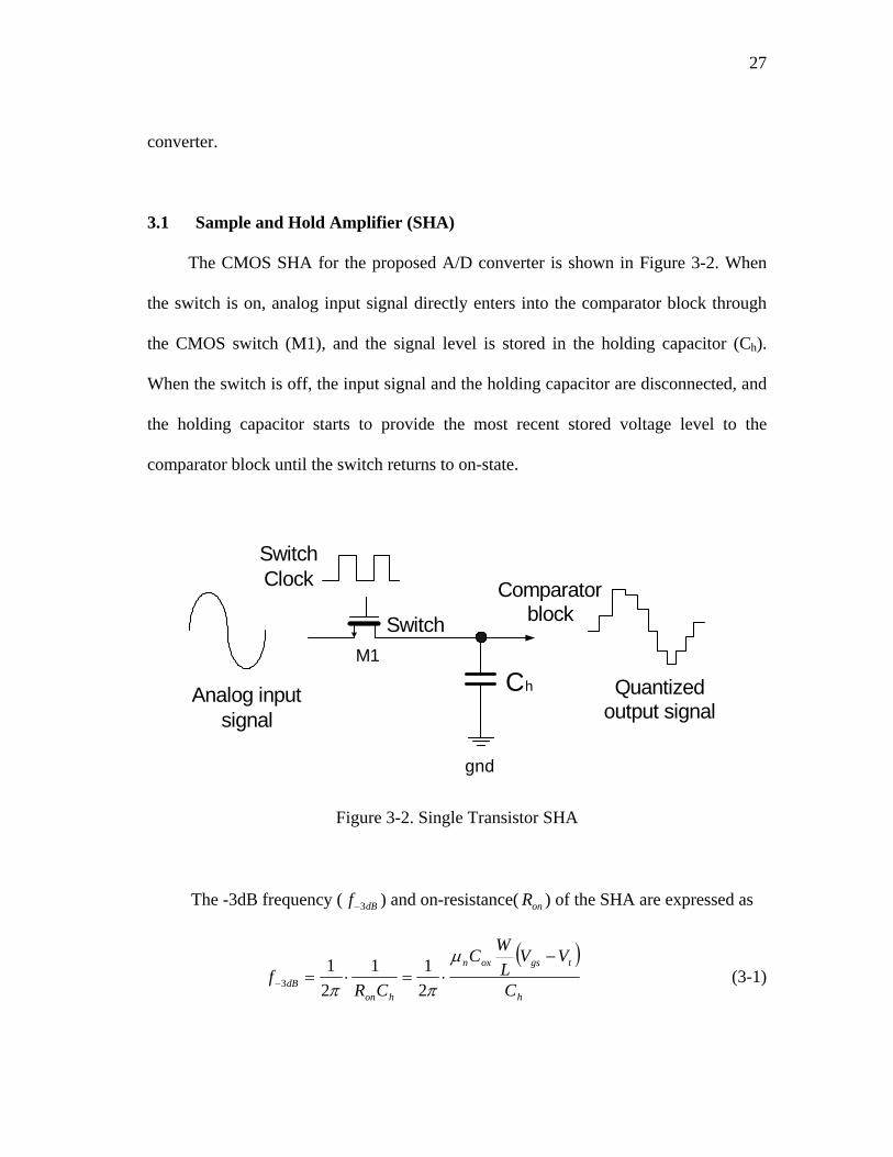
3.1 Sample and Hold Amplifier (SHA)
The CMOS SHA for the proposed A/D converter is shown in Figure 3-2. When
the switch is on, analog input signal directly enters into the comparator block through
the CMOS switch (M1), and the signal level is stored in the holding capacitor (Ch).
When the switch is off, the input signal and the holding capacitor are disconnected, and
the holding capacitor starts to provide the most recent stored voltage level to the
comparator block until the switch returns to on-state.
Switch
C h
SwitchClock Comparator
block
gnd
Analog input signal
Quantized output signal
M1
Figure 3-2. Single Transistor SHA
The -3dB frequency ( dBf 3− ) and on-resistance( onR ) of the SHA are expressed as
( )h
tgsoxn
hondB C
VVL
WC
CRf
−⋅=⋅=−
µ
ππ 211
21
3 (3-1)

28
( )tgsoxn
on
VVL
WCR
−=µ
1 (3-2)
where Vgs is the DC voltage between the gate and the source of M1. To realize high-
speed operation, large dimension of M1 is required. However, an increase in the
dimension of M1 is not recommended since the channel charge injection increases [13],
resulting in time-variant capacitance of the holding capacitor, which cause nonlinearity
at the SHA output signal [14]. To solve this problem, increasing Vgs of M1 is proposed
in this thesis using a voltage doubler [15][16].
M1 M 2
M3
M4
M5
M 6
C1 C2
Vdd
gnd1. 8 V
3.04 V
Vdd
gnd
AB Vout
V in
Cparasitic
Figure 3-3. Voltage Doubler

29
Figure 3-3 shows the voltage doubler circuit, utilizing a cross coupled transistors
(M1 and M2) with C1 and C2. It makes the node voltage of B boost to 2Vdd. The output
clock amplitude of the voltage doubler can be expressed by
222
CCCVV
parasiticddout +
⋅= (3-3)
where parasiticC represents the parasitic capacitance at the doubler’s output node.
The supply voltage of 1.8 V specified in Table 1-1 restricts the system clock
amplitude. The voltage doubler produces over 3.0 V clock amplitude, as shown in
Figure 3-4, which enables high-speed operation and small on-resistance of the SHA
Figure 3-4. Comparison of the Amplitude of the System Clock and the Voltage
Doubler Output Clock

30
3.2 Comparator Block
The proposed comparator is designed to improve the system bandwidth
degradation of a typical interpolating technique; and realize high gain in order to reduce
metastability error.
Figure 3-5 shows the realistic and ideal output waveforms of the comparator as
the analog input increases until the comparator digital output is ‘1’. When Vin=Vref,
those two lines meet at the point, defined as “transition point”.
Comparator Vref
Vout
Vin
( Ideal waveform )
( Realistic waveform )Transition point= Vdd/2
Vin (DC)gnd
Vdd
Vin = Vref
Vout
Vout
Figure 3-5. Transition Point
3.2.1 Reference Generator
The reference generator provides 8 reference voltage levels for the 8 comparators
in the proposed 4-bit interpolating structure. The reference generator based on a resistor

31
ladder structure is illustrated in Figure 3-6, and Table 3-1 shows the reference voltage
levels.
Vdd
gnd
Vref 8
Vref 4
Vref 3
Vref 2
Vref1
Vref 5
Vref 6
Vref 7
R=100 Ω
R=100 Ω
R=100
R=100 Ω
Ω
R=100 Ω
R=100
R=100 Ω
Ω
R=9 K Ω
R=9 K Ω
Figure 3-6. Resistor Ladder Reference Generator

32
Table 3-1. Reference Voltages
Reference node Value (V) Reference node Value(V) Vref1 0.669 Vref5 0.933 Vref2 0.735 Vref6 0.999 Vref3 0.801 Vref7 1.065 Vref4 0.867 Vref8 1.131
In the given specification, LSB was defined as 33mV. In Table 3-1, the difference
between two adjacent reference nodes is set as 66mV (=2 LSB) since the interpolating
technique realizes an additional reference point between two comparators and two node
voltages. Each reference voltage in Table 3-1 follows the equation:
Vref i = Vdd -Vref (9-i) (3-4)
3.2.2 Proposed Comparator Circuit
The proposed comparator consists of NMOS and PMOS dual input stages for the
differential inputs and the two reference voltage levels, as shown in Figure 3-7, which
satisfies the following equations.
2121 nnpp IIII === (3-5)
oMMMM
oxpMMMM
oxn KL
WCL
WC =⎟⎠⎞
⎜⎝⎛=⎟
⎠⎞
⎜⎝⎛
4,3,2,18,7,6,5
µµ (3-6)
iMMMM
oxpMMMM
oxn KL
WCL
WC =⎟⎠⎞
⎜⎝⎛=⎟
⎠⎞
⎜⎝⎛
16,15,14,1312,11,10,9
µµ (3-7)
|||| TnTp VV ≅ (3-8)

33
From Equation 3-5,
)(21|)|(
21
21
21
112
136211 TnsrefiTprefsiMMnp VVVKVVVKiiII −−=−−==== (3-9)
resulting in
131 2 refSS VVV =+ (3-10)
Similarly using 7311 21
21
MMnp iiII === , we can also derive
824 2 refSS VVV =+ (3-11)
gnd
Vdd VddVdd
p1
Vdd
p2
n1 n2gndgnd gnd
Vout+ Vout-Vref1 Vref 8 Vin-Vin +
M11 M12
M16M15M14M13
M9 M10
M7M6 M8M5
M4M3M2M1
VS1
VS3
VS2
VS4
Figure 3-7. Proposed Comparator

34
In the proposed comparator circuit, when Vin+ = Vref1 and Vin- = Vref8, Vout+ = Vout-
=Vdd/2. The difference between the differential inputs (Vin+ and Vin-) and reference
voltages (Vref1 and Vref8), respectively, is multiplied with the comparator’s gain,
resulting in the digital outputs Vout+ and Vout-.
As an example, if Vin+ > Vref1, the current through the M5 (iM5) exceeds iM6,
increasing iM13, and iM9 is decreased by the reduced Vsg_M1. At the same time, Vin- < Vref8
causes iM16 > iM12. Thus, the difference between iM13 and iM9 causes the digital output to
be Vout+ =’1’, and Vout- =‘0’.
From the above example, we can see that the difference between inputs and
reference voltages cause the difference between 13Mi and 9Mi , and 16Mi and 12Mi ,
resulting in the digital outputs (Vout+ and Vout-), which can be summarized as follows:
13Mi >> 9Mi and 16Mi << 12Mi +outV = ‘1’ and −outV = ‘0’ (Digital output)
13Mi << 9Mi and 16Mi >> 12Mi +outV = ‘0’ and −outV = ‘1’ (Digital output)
13Mi = 9Mi and 16Mi = 12Mi +outV = −outV = transition point
When Vin+ - Vref1 << 1 LSB and Vref8 - Vin- << 1 LSB, and the currents through
M13, M9, M12 and M16 are simple expressed as
2113 )( TnsiniM VVVKi −−= + (3-12)
239 |)|( TpinsiM VVVKi −−= + (3-13)
2412 )( TnsiniM VVVKi −−= − (3-14)
2116 |)|( TpinsiM VVVKi −−= − (3-15)
16Mi = 12Mi and 13Mi = 9Mi correspond to Vin-=Vref8 and Vin+=Vref1, respectively, as

35
a result of Equations (3-10)-(3-15). Therefore, the transition points of each comparator
output can be obtained when the input voltage meets its related reference voltage, which
was defined as “reference point” in the previous section.
Gain Boosting
The extra inverters are added at the comparator outputs, as shown in Figure 3-8,
in order to increase the comparator’s gain and reduce the rising/falling time of its output
signal.
gnd
Gain boosting inverters
Vdd VddVdd
Ip
Vdd
Ip
In Ingndgnd gnd
Vout + Vout -Vref 1 Vref 8 Vin +Vin -
Figure 3-8. Proposed Comparator with Extra Inverter Stages

36
AC simulation results with and without the extra inverters are shown in Figure 3-
9, where we can estimate that the gain increases by 25dB without significant bandwidth
degradation by the extra inverters. In addition, the transient responses show the digital
output signals of the both cases in Figure 3-10, and its slew-rate measurements
represent the reduced rising/falling time by the extra inverter stage.
Figure 3-9. AC Response

37
Figure 3-10. Transient Response (a) with (b) without Extra Inverter Stage
3.2.3 Proposed Interpolating Technique
The main goal of the interpolating technique is to reduce the number of
comparators in the flash A/D converter by creating an additional reference point from
two adjacent comparators. In Figure 3-11, the proposed interpolating architecture is
illustrated, where the two pairs of transistors (M1-M2 and M3-M4) are utilized instead
of the buffers and the resistors in the typical structure. The additional transistors satisfy
the following conditions.

38
12,104,2 MMoxn
MMoxn L
WCL
WC ⎟⎠⎞
⎜⎝⎛=⎟
⎠⎞
⎜⎝⎛ µµ (3-16)
7,53,1 MMoxp
MMoxp L
WCL
WC ⎟⎠⎞
⎜⎝⎛=⎟
⎠⎞
⎜⎝⎛ µµ (3-17)
Using Equation 3-5,
)(21|)|(
21
21
21
112
2'31426 TnSrefoTprefSoMMnp VVVKVVVKiiII −−=−−==== (3-18)
therefore, the relationship between VS1 and VS3’ can be derived as
LSBVVVVV refrefrefSS 22 1211'3 +⋅=+=+ (3-19)
Similarly using 192721
21
MMnp iiII === ,
LSBVVVVV refrefrefSS 22 8782'4 −⋅=+=+ (3-20)

39
gnd
Vdd VddVdd
IpVdd
Ip
In Ingnd
gnd gnd
Vref1 Vref8 V -Vin+
gnd
Vdd VddVdd
IpVdd
Ip
In Ingnd
gnd gnd
Vref 2 Vref7 V -V +
V
V
Vout1+
V
V
V
out2+
out3+
out1-
out 2-
out3-
M2
M8
M7
M4
M3M1
Next comparator Next comparator
M5
M6
M12
M11
M10
M9
in
in in
VS1 VS2
VS3 VS4
VS1' VS2'
VS3' VS4'
M13
M14 M15
M16
M17 M18 M19 M20
M21
M22 M23
M24
M25 M26 M27 M28
Figure 3-11. Proposed Interpolating Architecture
In Figure 3-11, M1-M4 are added to the two identical comparators, introduced in
Figure 3-7. From Equation 3-16 and 3-17, currents through M1-M4 can be expressed as

40
2151 )( TnSiniMM VVVKii −−== + (3-21)
2'3102 |)|( TpinSiMM VVVKii −−== + (3-22)
2473 )( TnSiniMM VVVKii −−== − (3-23)
2'1124 |)|( TpinSiMM VVVKii −−== − (3-24)
As previously stated, 13Mi , 9Mi , 16Mi and 12Mi determine the digital outputs of
Vout+ and Vout- in Figure 3-7. Similarly, the currents through M1, 2, 3 and 4 ( 1Mi , 2Mi ,
3Mi and 4Mi ) determine the digital outputs of Vout2+ and Vout2- in the proposed
architecture, which can be summarized as
iM1 >> iM2 and iM3 << iM4 +2outV = ‘1’ and −2outV = ‘0’ (Digital output)
iM1 << iM2 and iM3 >> iM4 +2outV = ‘0’ and −2outV = ‘1’ (Digital output)
iM1 = iM2 and iM3 = iM4 +2outV = −2outV = transition point
Let us defied the reference points Vx+ and Vx-, such that when iM1 = iM2 and iM3 =
iM4 , when Vin-= Vx- and Vin+= Vx+. Although Vx+ and Vx- provide the reference points
for the Vout2+ and Vout-, they are not from the reference generator. The additional
transistor pairs realize the interpolating architecture by providing the additional
reference point (Vx+) from two reference voltage (Vref1 and Vref2) and two adjacent
comparators. Vx+ and Vx- can be derived as follows.

41
2'3
2121 |)|()( TpinSiTnSiniMM VVVKVVVKii −−=−−⇒= ++
LSBVLSBVVVVV refSSSSin 2222 1131'3 +=++=+=⋅⇒ + (3-25)
after simplification.
++ =+=⇒ xrefrefin VVVV 2/)( 21 (3-26)
Similarly,
−− =+=⇒ xrefrefin VVVV 2/)( 87 (3-27)
As shown in Equations 3-26 and 3-27, the additional reference point by the
proposed interpolating architecture indicates the averaged value of two adjacent
reference voltages, which satisfies the requirement of the additional reference point by
the typical interpolating structure described in previous chapter.
In Figure 3-12, each output characteristics of the proposed architecture in Figure
3-11 are illustrated for the DC input sweep with the reference points by the interpolating
technique. As shown in Figure3-12, the output characteristics of Vout2+,– represent digital
outputs for the DC input sweep like the outputs of the comparators, and, the reference
point, realized by the interpolating technique, indicate the averaged value of Vref1 and
Vref2, as defined in Equation 3-26 and 27.

42
Vin+
Vin+
Vref1
Vref8
Vref2
Vref7
Transition Point (=0.9V =Vdd/2)
Vout1+Vout2+
Vout3+
Vout1-
Vout2-
Vout3-
0.669 V 0.735V0.702V
Vin=Vref1 Vin=Vref2Vin=(Vref1+Vref2)/2Offset point by
comparatorOffset point by
comparatorOffset point by interpolating
technique
(DC)
1 LSB1 LSB
Vin=Vref1
Reference point in comparator
Vin=Vref2
Reference point in comparator
Vin=(Vref1+Vref2)/2Reference point by interpolating
architecture Figure 3-12. DC Simulation Results of the Proposed Interpolating Architecture
Comparison between the Proposed and the Typical Interpolating Architectures
In the Figure 3-13, the left half realizes the proposed interpolating architecture
and the right half implements the typical structure employing buffers and resistors in
order to provide the comparison results of the both topologies for the bandwidth.

43
gnd
Vdd VddVdd
Ip
Vdd
Ip
In Ingndgnd gnd
Vref1 Vref8 VIn-VIn+
gnd
Vdd VddVdd
Ip
Vdd
Ip
In Ingndgnd gnd
Vref2 Vref7 VIn-VIn+
BufferV
V
Vout1+
V
V
V
out2+
out3+
out1-
out2-
out3-
S1
S3'
S2'S1'
S4S3
S2
S4'
R
R
Figure 3-13. Comparison of the Typical and Proposed Interpolating Architecture
As shown in Figure 3-14, the proposed interpolating structure does not cause any
significant bandwidth degradation as compared with the AC response of Figure 3-9, but
the -3dB frequency of the typical structure is dramatically reduced by the buffers and
the resistors. Therefore, it can be concluded that the proposed comparator mitigates the

44
main drawback of the typical interpolating structure.
Figure 3-14. AC Response of the Typical and Proposed Interpolating Architecture

45
3.3 The First Latch Block
The 1st latch block in the proposed A/D converter consists of 15 latches, one of
which is illustrated in Figure 3-15
CLK
CLK
CLK
M1 M2M5 M6
M3 M4
M7 M8
A B
M9
Vin+Vin-
VddVdd Vdd
gnd
gnd gnd
Vout- Vout+
Figure 3-15. Latch
The input Vin- and Vin+ are directly connected to the differential outputs of the
comparator, discussed in the previous section. The latch clock signal (CLK) determines
the tracking and holding states through M7 and M8. In tracking mode, the CLK is high,
and the amplified differential input signals appear on the nodes A and B through M7
and M8. In holding mode, the CLK goes low, and M7 and M8 disconnect nodes A and
B from the input signals. Therefore, the most recent tracking value is held at the nodes
A and B during the holding state. The inverters at the ends of the latch are used to
improve the metastability error [1].

46
3.4 Encoder
The parallel-connected comparator and latch pairs in the proposed interpolating
A/D converter produce thermometer code from analog input signal; therefore, the
thermometer code should be converted into the binary code for the DSP system.
Thermometer code is represented by a series of j consecutive ‘0’s and a following
series of k consecutive ‘1’s (j+k=m for m bit thermometer code). The number of ‘1’s in
the code represents decimal number, as shown in Figure 3-16. m-bit binary code [Dm-1
Dm-2 Dm-3… D0 ] represents the decimal value of D m-12m-1+ D m-22m-2
+ D m-32m-3+…+ D
020, as shown in Figure 3-16
Binary code 00010010001101000101
Thermometer code
…
000000000000001
…
000000000000011000000000000111000000000001111000000000011111
Decimal12345
…
Figure 3-16. Thermometer and Binary Codes for Decimal Numbers

47
Binary code
[ 0 0 1 1 ]
Thermometer code
[ 0 0 0 0 0 0 0 0 0 0 0 0 1 1 1 ]
B-Code1
Code6Code7Code 9 Code8Code10Code 12Code11Code13Code 15 Code14
B-Code4 B-Code3 B-Code2
Code5 Code1Code2Code3Code4
Figure 3-17. Thermometer and Binary Codes for the Decimal Number 3
In Figure 3-17, the 4 bit thermometer and binary code represent decimal number
3, and the binary code [B-Code4, B-Code3, B-Code2, B-Code1] can be encoded from
the thermometer code by the following logical descriptions
B-Code1 = (Code1+Code3+Code5+Code7+Code9+Code11+Code13+Code15 ) (3-26)
B-Code2 = (Code2+Code3+Codee6+Code7+Code10+Code11+Code14+Code15) (3-27)
B-Code3 = (Code4+Code5+Code6+Code7+Code12+Code13+Code14+Code15 ) (3-28)
B-Code4 = (Code8+Code9+Code10+Code11+Code12+Code13+Code14+Code15) (3-29)
The encoder block of the proposed A/D structure realizes the above encoding
descriptions with OR gates as illustrated in Figure 3-18.

48
code 2code 3code 6code 7
code10
code14
code11
code15
B- Code 2
code 8code 9code 10code 11
code12
code14
code13
code15
B- Code 4
code 1code 3code 5code 7
code 9
code13
code11
code15
B- Code 1
code 4code 5code 6code 7
code 12
code14
code13
code15
B- Code 3
Figure 3-18. Implementation of the Proposed Interpolating A/D Converter Encoder
3.5 The Second Latch Block
For a dual-in-line package (DIP), the die is planted in cavity, which is bonded to
the pads through the perimeter and such a structure causes parasitic package
capacitance and inductance [12]. To show the impact of parasitic package inductance at
the converter output buffer stage, a digital output buffer is depicted in Figure 3-19 with
a load capacitor(CL) and package inductances on supply and ground (LVdd and Lgnd) [3].

49
0.94ns
CL
gnd
gnd
A
B
Raising time Falling time
t
effective data width
0.74ns0.2ns 0.2ns
t
Lvdd
Lgnd
Vdd
Encoder output Converter output after output digital buffer
M2
M1
Figure 3-19. Digital Output Buffer with Parasitic Package Inductance
The digital buffer includes a load capacitor at its output node, which increases the
rising/falling time of the digital output signal as described in
t rising/falling ( ) ⎟⎟⎠
⎞⎜⎜⎝
⎛⎟⎟⎠
⎞⎜⎜⎝
⎛ −+
−−⋅
=dd
tdd
tdd
t
tdd
total
VVV
VVV
VVKC 43ln
212 (3-30)
where 21 2
121
Moxp
Moxnpn L
WCL
WCKKK ⎟⎠⎞
⎜⎝⎛=⎟
⎠⎞
⎜⎝⎛=== µµ and totalC represents the
total capacitance at the output node. In order to decrease the rising/falling time, a large
output buffer is required, which increases the dynamic power.
The currents during the rising/falling time can be expressed by
tVCI total ∆
∆= (3-31)
where V∆ =Vdd-0 and t∆ represents the desired rising/falling time of the converter
digital output signal [17]. We can estimate the voltage changes at the node A and B

50
from the expressions
tILV VddAnode ∆
∆=_ ( 3-32 )
tILV gndBnode ∆
∆=_ ( 3-33 )
The voltage transmitters at nodes (A and B) for continuous digital inputs are
known as ‘supply bounce’ and ‘ground bounce’, respectively [3][17].
With the assumptions of 5pF of total capacitance and Lvdd = Lgnd = 2nH, the
supply and ground bounce are estimated as 450mV each for the 0.2ns of the
rising/falling time. To reduce the bounces, more rising/falling time of converter digital
output signal are required. With the 0.4ns of the rising/falling time, the supply and
ground bounce are degraded to 112.5mV. However, the increased rising/falling time
reflect the less effective data width, where well-defined digital value is provided to the
DSP system; therefore, the small effective data width increases the jitter sensitivity of
the DSP system. Hence, the 2nd latch block is proposed to relieve the requirements of
the fast rising/falling time with more effective data width.
In the proposed A/D converter, the encoder output signal has the data streaming
width of 0.94ns. Therefore, to obtain the effective data width of 0.74ns, 0.2ns
rising/falling time is required. However, even with the increased rising/falling time
(0.4ns), the more effective data width (1.44ns) can be obtained in the 2nd latch block by
doubling the encoder output data streaming width as shown in Figure 3-20. The doubled
data streaming width reduces the jitter sensitivity of the DSP system and increases the
more effective data width, which relaxes the requirement of the fast rising/falling time,

51
resulting in the less bounces.
Falling time0.74ns0.2ns 0.2ns
t
t
Rasining time
Falling time0.4ns 0.4ns
Rasining time effective data width
1.48ns
Digital output signal without 2nd latch block
( 0.94ns data width )
Digital output signal with 2nd latch block( 1.88ns data width )
effective data width
Figure 3-20. Encoder Output and Doubled Encoder Output by the 2nd Latch Block
Because the DSP system only uses the captured input digital value at sampling
points, the output of the encoder and the 2nd latch block represent the same results at the
DSP system, as shown in Figure 3-21.

52
System Clock Signal (528MHz)
0.94ns
Encoder output
Proposed 2nd latch output
Sampling points of the DSP system
1 1 10 0 Result at the DSP sampling points
Figure 3-21. Encoder and the Proposed 2nd Latch Output at the DSP Sampling Points
In Figure 3-21, the proposed 2nd latch block doubles the data streaming width of
the encoder output. At the DSP sampling points, the encoder output and the 2nd latch
output reflect same results of [1 1 0 0 1] but the more effective data width is provided
by the 2nd latch block.
As shown in Figure 3-22, the 2nd latch block consists of 4 sub-blocks, and each
sub-block consists of 2 latches and an OR gate.

53
Latches
CLK CLK
Second Latch Block ( 4 sub-blocks )
CLK CLK
Binary Input( 0.94 ns data streaming width)
Binary output( ns data streaming width )
ns data streaming width
ns data streaming width
ns data
OR gate
D Q D Q
inverter inverter
0.94
1.88
1. 88
First latch Second latch
Figure 3-22. Block Diagram of the 2nd Latch Block

54
CLK CLK
D Q D Q
inverter inverter
CLK
CLK
CLK
CLK CLK
CLK
CLK
CLK
Input from encoder
OUT 1 OUT
Input from encoder
2
OUT 1OUT 2
Vdd
gnd
Vdd
VddVdd
gnd gnd gnd
First latch Second latch
Figure 3-23. 2nd Latch Block in Transistor Level
The transistor level implementation of the latches is shown in Figures 3-23,
where the first latch captures and holds the output signal of the encoder when the clock
is low, and then the second latch senses and holds the output signal of the first latch
when the clock goes high. Therefore, using the 528MHz system clock frequency, the
first latch holds the encoder output signal for 0.94ns and the second latch holds the
output value of the first latch for 0.94ns with the delay of 0.94ns. These two output
signals of the latches are added by the OR gate; hence, the output of the OR gate
represents the doubled data width (1.88ns =0.94ns+0.94ns) of the encoder output signal.
The transient simulation results for the 2nd latch block are shown in Figure 3-24.

55
Figure 3-24. Transient Response of the 2nd Latch Block
From Figure 3-24, we can see that the encoder output signal (signal A) is detected
and kept by the first latch (signal B) during 0.94ns, which is copied by the second latch
(signal C) with the delay of 0.94ns. The output signals (signal B and C) are added by
the OR gate, which causes the doubled width of the encoder output signal (signal D).

56
3.6 Clock Synchronization Block
The clock synchronization block provides clock signals to the SHA, the 1st latch
block and the 2nd latch block as shown in Figure 3-25. The input clock signal of the
clock synchronization block comes from the PLL circuit in the same UWB chip. To
synchronize the clocks and the performances of each block in the proposed A/D
converter, clock delays are required, which are implemented by the digital clock buffers
in the clock synchronization block, as shown in Figure 3-25.
Clock from PLL Clock Synchronization Block
SHA1 st Latch
block2nd Latch
block
SHA 1st Latch block 2 nd Latch block
Clock from PLL
Figure 3-25. Clock Synchronization Block

57
CHAPTER IV
SIMULATIONS OF THE PROPOSED A/D CONVERTER
To measure the A/D converter’s performance, static and dynamic simulations are
used. Static simulation mainly represents the performance of the comparator block and
dynamic simulation shows the results of nonlinearities and distortions for the various
input frequencies.
4.1 Static Simulation
Figure 4-1 shows the DC response of the comparator block as the input voltage is
swept from 0.2V to 1.6V.
Figure 4-1. DC Response

58
Each line in Figure 4-1 indicates the digitized output of the comparator block
including interpolating architecture described in section 3.2. Figure 4-2 shows the step
response of the A/D converter.
Figure 4-2. Step Response of the A/D Converter
From the Figure 4-2, we can measure the INL= 0.071 LSB and the
DNL=0.126LSB. Figure 4-3 and 4-4 shows the INL and DNL, respectively, at 0 oC and
125 oC.

59
INL
-0.1
-0.05
0
0.05
0.1
0.15
1 2 3 4 5 6 7 8 9 10 11 12 13 14 15
Code
LSB
INL= 0.095 LSB when temperature = 0 oC
INL
-0.1
-0.05
0
0.05
0.1
0.15
1 2 3 4 5 6 7 8 9 10 11 12 13 14 15
Code
LSB
INL = 0.093 LSB when temperature = 125 oC
Figure 4-3. INL for Temperature Variations

60
DNL
-0.2
-0.15
-0.1
-0.05
0
0.05
0.1
0.15
0.2
1 2 3 4 5 6 7 8 9 10 11 12 13 14
Code
LSB
DNL = 0.164 LSB when temperature = 0 oC
DNL
-0.2
-0.15
-0.1
-0.05
0
0.05
0.1
0.15
0.2
1 2 3 4 5 6 7 8 9 10 11 12 13 14
Code
LSB
DNL = 0.154 LSB when temperature = 125 oC
Figure 4-4. DNL for Temperature Variations
The static simulations for the various temperature conditions result in (its .)
Within the temperature range from 0oC to 125oC, DNLmax =0.164 LSB and
INLmax=0.095 LSB are achieved. The maximum value as given in Table 1-1 is 0.5 LSB.

61
4.2 Dynamic Simulation
Dynamic simulation is very important for high frequency A/D converters because
their nonlinearities and distortions increase as the input frequency and the sampling
frequency increase.
4.2.1 SINAD and SFDR
Figure 4-5 shows the SINAD and SFDR results obtained from fast fourier
transform (FFT) for the various input frequencies.
Figure 4-5. SFDR and SINAD
From Figure 4-5, 3.75 ENOB is achieved at 265MHz using Equation 1-2, which

62
satisfies the ENOB specification (>3.6) in Table 1-1. Moreover, the estimated ENOB
indicates that the proposed A/D converter can handle higher sampling frequencies over
the given specification (528Mhz) since the maximum sampling frequency is determined
by the frequency where the ENOB gets -0.5 bit degradation [1].
4.2.2 Dynamic Simulations for Temperature Variation
Dynamic simulation are also proposed at 0oC and 125oC temperatures.
Simulation conditions are as follows:
Sampling frequency : 528MHz
Input signal : Differential 1 Vp-p at 259MHz and 263MHz
Corner simulation : Temperature (0 oC ~125 oC)
Sampling point : 528
Figure 4-6 to 4-9 shows the simulation results, which are classified in Table 3-1.

63
Figure 4-6. FFT Result When Temperature = 0 oC (259MHz Input Frequency)
Figure 4-7. FFT Result When Temperature = 125 oC ( 259MHz Input Frequency)

64
Figure 4-8. FFT Result When Temperature = 0 oC (263MHz Input Frequency)
Figure 4-9. FFT Result When Temperature = 125 oC ( 263MHz Input Frequency)

65
Table 4-1. FFT Results for Temperature Variations
Temperature = 0 oC Temperature = 125 oC
Input frequency 259MHz 263MHz 259MHz 263MHz
SINAD (dB) 24.77 24.16 25.54 25.64
ENOB (bit) 3.82 3.72 3.95 3.96
SFDR (dB) 31.52 30.71 33.24 34.36
THD (dB) -28.73 -27.37 -31.30 -32.29
From Table 4-1, we can see that SINAD, ENOB and SFDR satisfy the
requirements specified in chapter I within the temperature range 0oC ~125oC.
4.3 Layout and Summary of Simulation Results
The layout in Figure 4-10 shows the proposed interpolating A/D converter
realized with its seven sub-blocks introduced in chapter II, and two additional blocks
(the current control and the clock select switch block). The layout are used in 390 µm
×320 µm.
The clock select switch block enables using not only the internal PLL clock
signal but also an external clock signal as the converter input clock. The current control
block enables the use of multiple choice of bias currents (Ip and In) for the comparator
described in Figure 3-5 in order to compensate the mismatch of the bias currents (Ip and
In).

66
320um
390um
Figure 4-10. Layout of the Proposed A/D Converter

67
Summary of simulation results for the proposed interpolating A/D converter is
given in Table 4-2.
Table 4-2. Simulation Results of the Proposed A/D Converter
Specification Value Input Differential 1 Vp-p
Input Frequency < 264 MHz Sampling Frequency 528 MHz
Resolution 4 bit LSB 33mV SNR 25.84 dB
SINAD @ 263MHz 24.77 dB SFDR @ 263MHz 31.52 dB ENOB @ 263MHz 3.82 bit THD @ 263MHz -28.73 dB
INL 0.095 LSB DNL 0.164 LSB Size 390 µm × 320 µm
Power Consumption 6.93mW
Table 4-3 shows the comparison between the proposed interpolating A/D
converter and three other references. The proposed work has significantly low power
dissipation and smaller chip area, and achieves 6GHz bandwidth. It can be concluded
the proposed A/D converter possesses the advantages of both the interpolating and the
flash converters without the disadvantages of either.

68
Table 4-3. Various A/D Converter Publications (MSF=Maximum Sampling Frequency)
Specification Proposed A/D converter [18] [19] [20]
Published 2005 2004 2004 1999 Input Signal
Range Differential
1V Differential
1 V Differential
0.88 V Differential
2 V MSF 6.01 GHz 5.0GHz 3.2 GHz 12 GHz
Resolution 4 bit 4 bit 4 bit 4 bit INL 0.095 LSB 0.34 LSB 0.6 LSB 0.4 LSB DNL 0.164 LSB 0.24 LSB 0.4 LSB 0.4 LSB
Chip Area 0.124 mm2 0.2 mm2 0.4 mm2 9 mm2 Power
Consumption 9.61mW 70mW 131mW 1.0 W
Technology 0.18 µm CMOS
0.18 µm CMOS
0.18 µm CMOS
0.25 µm CMOS
Supply Voltage 1.8 V 1.8 V 1.8 V 2.5 V

69
CHAPTER V
DIGITAL-TO-ANALOG CONVERTER
Digital-to-analog converters (D/A converter) generate analog output signals for
given digital input codes, and mainly consist of a decoder and a reference generator as
shown in Figure 5-1. The decoder converts the binary output code of the DSP system
into the thermometer, and the reference generator creates a certain reference level for
the thermometer code resulting in an analog signal.
Decoder Reference generator
D/A ConverterBinary code Analog signal
Thermometer code
Figure 5-1. D/A Converter
The following sections introduce the proposed differential D/A converter, which
consist of a binary to thermometer decoder and a differential reference generator.

70
5.1 Decoder
The proposed D/A converter employs a binary-to-thermometer decoder to reduce
the glitch error [1]. In the decoder, the binary input code is converted into the
thermometer code through the logical descriptions in Figure 5-2.
Binary input code
Thermometer output code
[ D C B A ]
[ T15 T14 T13 T12 T11 T10 T9 T8 T7 T6 T5 T4 T3 T2 T1 ]
Binary input code
A = 2 0
B = 2 1
C = 2 2
D = 2 3
Thermometer output code
A+B+C+DB+C+D
AB+C+DC+D
AC+ BC+DBC+DABC+D
DAD+BD+CD
BD+CDABD+CD
CDCD(A+B)
BCDABCD
T 1 :T 2 :T 3 :T 4 :T 5 :T 6 :T 7 :T 8 : T 9 :T 10 :T 11 :T 12 :T 13 :T 14 :T 15 :
Figure 5-2. Decoding from Binary to Thermometer Code

71
5.2 Reference Generator
The proposed reference generator is illustrated in Figure 5-3. The resistors (R1,
R2,…, R15) are either connected to gnd to Vdd, depending on the thermometer output
code of the decoder.
R 1
R 2
R 7
R 8
R 9
R 14
R 15
Vdd
Vout
Controlled by Thermometer code
R gnd
R Vdd
gnd
gnd
gnd
gnd
gnd
gnd
gnd
gnd
Vdd
Figure 5-3. Proposed Reference Generator
If all the resistors have the same value (R1= R2…=R15=R), Vout can be

72
expressed as
( )
( ) ( )
dd
Vddgnd
gndout V
RTH
RRTH
R
RTH
RV
11_11
10_11
10_11
+⋅+
+⋅
+⋅
=
∑∑
∑ (5-1)
where TH_1 is the number of logical ‘1’s in thermometer code and TH_0 is the number
of logical ‘0’s in thermometer code. The output swing range of the decoder is
determined by RVdd and Rgnd. The upper and lower limit of the output swing range were
estimated as 1.125V and 0.675V in chapter I, which can be obtained by Rgnd =RVdd
=1.9kΩ and R= 40kΩ based on the Equation 5-1.
R
Vdd
Rgnd
RVdd
gnd
R R R
R R
Resistor number is determined by the switch connection of Vdd-R
Resistor number is determined by the switch connection of gnd-R
Vout
Figure 5-4. Output Reference Voltage Determined by the Parallel Resistance When
R1= R2…=R15=R

73
The following sections describe the features of the proposed reference generator
including full output swing, high speed operation and differential structure.
5.2.1 Full Output Swing
Although the output swing is limited to 0.45 V by resistors to satisfy the given
specifications in the proposed reference generator, its output can get full swing by
eliminating Rgnd and RVdd. Therefore, the proposed topology can be a solution of the
D/A converter requiring large output range.
5.2.2 High Speed Operation
Figure 5-5 shows the implementation of switch (see Figure 5-3) by an inverter.
Although the accumulated parasitic capacitance at an output node by the parallel-
connected resistors cause the bandwidth degradation of the output signal in the
proposed topology, the large dimension of the inverter switch enables the fast output
response possible for the digital input code.

74
R3
R4
R5
Vdd
Output
Thermometer code
R4
Vref
gnd
gnd
gnd
gnd
Figure 5-5. Inverter Switch
Figure 5-6 shows the transient response of the proposed reference generator and
the known as voltage division topology, presented in [1][3]. To emphasize the fast
performance of the proposed reference generator, the reduced input data streaming
width (1ns) is applied instead of 1.88ns. In Figure 5-6, the proposed topology retains its
sharp edges even in narrower width case, but the voltage division topology does not
demonstrate a similar level of speed. In addition, the voltage division topology shows
the distortion over 1.1 V because the increased on-resistance of the switches limits its
output swing range. However, the proposed topology keeps its sharp edge over 1.1 V
without significant distortion because the proposed topology enables full output swing
range as described in the previous section.

75
Proposed reference generator
Voltage division reference generator
Figure 5-6. Transient Responses of the Voltage Division and the Proposed Reference
Generator
5.2.3 Differential Structure
Although the proposed reference generator has a single output in Figure 5-2,
differential operation is desired to fulfill the requirements. By inverting the
thermometer code, we can produce the differential voltage level as follows:
( )
( ) ( )
dd
Vddgnd
gndout V
RTH
RRTH
R
RTH
RV
10_11
11_11
11_11
+⋅+
+⋅
+⋅
=
∑∑
∑−
(5-2)

76
( )
( ) ( )
dd
Vddgnd
gndout V
RTH
RRTH
R
RTH
RV
11_11
10_11
10_11
+⋅+
+⋅
+⋅
=
∑∑
∑+
(5-3)
Equation 5-2 and 5-3 are based on Equation 5-1; Vout+ is obtained through the
proposed structure in Figure 5-2 and Vout- is realized by applying the inverted
thermometer code which is obtained by an additional inverter block as shown in
Figure 5-7.

77
Inverter block
Binary -to-Thermometer
decoderBinary code
Reference generator Vout+
Vout-Reference generator
[ 111100000000000 ]
[ 0000111111111111 ]Thermometer code
Inverted thermometer code
Vdd
gnd
Vdd
gnd
Vdd
gnd
[ 111100000000000 ]
Invertedthermometer code
[ 0000111111111111 ]
Thermometer code
Figure 5-7. Block Diagram of the Differential Reference Generator

78
CHAPTER VI
SIMULATIONS OF THE PROPOSED D/A CONVERTER
6.1 Static Simulation
In Figure 6-1, the differential discrete output signals are obtained by the proposed
D/A converter for the binary ramp code.
Differential Output Result through the Differential
reference structure in Figure 5-7 (Vout-)
Differential Output Result through the Differential
reference structure in Figure 5-7 (Vout+)
Figure 6-1. Transient Response for the Proposed D/A Converter

79
INL
-0.3
-0.25
-0.2
-0.15
-0.1
-0.05
0
0.05
0.1
1 2 3 4 5 6 7 8 9 1 11 12 13 14 15 16
CODE
LSB
DNL
-0.04
-0.02
0
0.02
0.04
0.06
0.08
1 2 3 4 5 6 7 8 9 1 11 12 13 14 15
CODE
LSB
Figure 6-2. INL and DNL
Figure 6-2 shows that DNL = 0.06 LSB and INL = 0.26 LSB, which satisfy the
requirements of the proposed D/A converter.
6.2 Dynamic Simulation
To see the influence of the dynamic nonlinearities, the simulation results shown
in Figure 6-3 is used with the following conditions:
Minimum data streaming width : 1.88ns

80
Input signal : 1 Vp-p / 21MHz
Sampling Point : 528
The FFT result of the proposed topology and the ideal one are provided in Figure
6-4, respectively.
Proposed D/A Converter
Ideal D/A Converter
Ideal A/D Converter FFT conversion
Binary code
Analog input signal
analog signal
analog signal
Figure 6-3. Dynamic Simulation Setup
Figure 6-4. FFT Result of the Ideal D/A Converter

81
Figure 6-5. FFT Result of the Proposed D/A Converter
Table 6-1. Dynamic Simulation Results of the Ideal and Proposed D/A Converter
Ideal D/A converter Propose D/A converter SINAD 24.9189 dB 24.7368 dB ENOB 3.85 bit 3.82 bit THD -40.9888 dB -40.9888 dB SFDR 41.5533 dB 41.5533 dB
As shown in Table 6-1, the difference of the SINAD of the both topologies is
0.1821 dB, which indicates 0.03 ENOB degradation of the proposed D/A converter.

82
6.2 Layout and Summary of Simulation Result
The layout of the proposed D/A converter shows the distributed input paths, the
decoder and the differential reference generator in Figure 6-6. The total chip area is 280
µm ×130 µm.
280um
130um
DifferentialReference Generator
Decoder
Input Path
Figure 6-6. Layout
Table 6-2 shows the summary of simulation result for the proposed D/A converter.
Although small chip area is achieved, 19.04mW of power consumption is required. This
can be reduced by increasing the resistor values of the reference generator, which
decreases the bandwidth due to accumulated parasitic capacitance at the output node.

83
Table 6-2. Simulation Results of the Proposed D/A Converter
Specification Value Input 4-bit binary
Data streaming width 1.88 ns DNL 0.26 LSB INL 0.06 LSB
Output Range 0.45 V Size 130 µm x 286 µm LSB 30mV
Power Consumption 19.04mW Supply voltage 1.8 V
Process TSMC 0.18 µm

84
CHAPTER VII
CONCLUSIONS
The main design goals of the proposed A/D converter is to achieve the high-
speed and low-power requirements within a small chip area. The proposed topology is
based on interpolating technique, which reduces the problems caused by the large
number of comparators in a typical flash A/D converter. In this thesis, an alternative
interpolating architecture is proposed. Buffers and resistors of the typical interpolating
structure are replaced with a pair of CMOS transistors which solves the bandwidth
degradation problem. It can be concluded that the proposed interpolating A/D converter
eliminate the major disadvantages of the flash and the interpolating converter structures.
The proposed comparator within the A/D converter realizes high gain by adding
extra inverters at its output nodes, which reduces the possibility of bit errors caused by
metastability. The proposed 2nd latch block decreases the distortion at the converter’s
output digital signal and the jitter sensitivity of the DSP system by doubling the data
streaming width of the encoder output signal.
Although the proposed A/D converter is designed for 528MHz sampling
frequency, its dynamic simulation results shows the possibility of faster sampling
frequency with low power dissipation characteristics and compact chip area.
In addition, an D/A converter has been proposed in this thesis for an UWB
transmitter. The proposed D/A converter has advantages such as full swing output range,

85
high speed operation and differential structure.

86
REFERENCES
[1] R. J. van de Plassche, CMOS Integrated Analog-to-Digital and Digital-to-Analog
Converters: Boston, MA: Kluwer Academic Publishers, 2003.
[2] Y. Gendai, Y. Komatsu, S. Hirase, and M. Kawata, “An 8b 500MHz ADC,” in
Proc. IEEE International Solid-State Circuits Conference, pp. 172-173, Feb.
1991.
[3] F. Goodenough, “Interpolators put 10-bit 75MHz A/D converters on 8-bit digital
process,” Electronic Design, vol. 17, no. 11, pp . 29-30, Dec. 1989.
[4] X. Jiang, Y. Wang, A. Willson, “A 200MHz 6-bit folding and interpolating m
CMOS,” ADC in 0.5 in Proc. IEEE International Symposium on Circuits and
Systems, vol. 1, pp.5-8, June 1998.
[5] Ugur Cilingiroglu, Systematic Analysis of Bipolar and MOS Transistors, Norwood
MA, Artech House, 1993.
[6] Behzad Razavi, Principles of Data Conversion System Design, New York: IEEE
Press, 1995.
[7] R. J. Plassche and J. Van Valburg, “An 8-bit 650MHz folding ADC,” IEEE
Journal of Solid-State Circuits, vol. 27, no.6, pp. 1662-1666, Dec. 1992.
[8] Michael J. Deemler, High-speed Analog-to-digital Conversion, New York:
Academic Press, Inc.1991.
[9] Y. Akazawa, A. Iwata, T. Wakimoto, T. Kamato, H. Nakamura, and H. Ikawa,
“A 400 MSPS 8-b flash A/D conversion LSI,” in Proc. IEEE International Solid-

87
State Circuits Conference, pp. 27-28, Feb.1987.
[10] M. Choi, A. Abidi, “A 6-b 1.3-Gsample/s A/D converter in 0.35- µm CMOS,”
IEEE Journal of Solid-State Circuits, vol. 36, no. 12, pp. 1847-1858, Dec. 2001.
[11] M. Flynn and D. Allstot, “CMOS folding ADC’s with current-mode
interpolation,” IEEE Journal of Solid-State Circuits, vol. 31, no. 13, pp. 1248-
1257, Sept. 1996.
[12] M. Flynn and B. Sheahan, “A 400-Msample/s, 6-b CMOS folding and
interpolating ADC,” IEEE Journal of Solid-State Circuits, vol. 33, no. 9, pp.
1932-1938, Dec. 1998.
[13] J. U. Horstmann, H. W. Eichel, and R. L. Coates, “Metastability behavior of
CMOS ASIC flip-flops in theory and test,” IEEE Journal of Solid-State Circuits,
vol. 24,no. 14, pp. 146-157, Feb. 1989.
[14] D. Johns and K. Martin, Analog Integrated Circuit Design, New York: John
Wiley & Sons, Inc., 1997.
[15] R. J. Plassche, Integrated Analog-to-Digital and Digital-to-Analog Converters,
Dordrecht, The Netherlands: Kluwer Academic Publishers, 1994.
[16] I. Mehr and D. Dalton, “A 500-MS/s, 6-bit Nyquist-rate ADC for disk-drive
readchannel applications,” IEEE Journal of Solid-State Circuits, vol. 34, no. 24,
pp. 912-920, Dec. 1999.
[17] T. Yamamoto, S. Gotoh, T. Takahashi, K. Irie, K. Ohshima, “A mixed-signal
0.18 µm CMOS SoC for DVD systems with 432M Samples/s PRML read
channel and 16Mb embedded DRAM,” IEEE Journal of Solid-State Circuits, vol.

88
36, no. 17, pp. 1785-1794, Nov. 2001.
[18] F. Maloberti, F. Francesconi, P.Malcoverti, O.J.A.P.Nys, “Design consideration
on low-voltage low-power data converters,” IEEE Trans. Circuit and Systems-I,
vol. 42, no. 21, pp. 653-863, Nov.1995.
[19] S. Naraghi and D. Johns, “A 4-bit analog-to-digital converter for high-speed
serial links”, in Proc. Micronet Annual Workshop, April 26-27, 2004, Aylmer,
Quebec, Canada, pp. 33-34.
[20] W. Ellersick, C. K. Yang, M. Horowitz, and W. Dally, “GAD: A 12GS/s CMOS
4-bit A/D converter for an equalized multilevel link,” IEEE Symp. VLSI Circuits,
Dig. Tech. Papers, June 1999, pp. 49-52.
[21] S. Sheikhaei, S. Mirabbasi, and A. Ivanov, “A 4-Bit 5GS/s flash A/D converter
in 0.18µm CMOS” in Proc. IEEE Int. Symp Circuit and Systems (ISCAS), May
2005, pp.6138-6141

89
VITA
Name: Choong Hoon Lee
Address: 236 Tally Ho Road
Killeen, TX, 76542
Email Address: [email protected], [email protected]
Education: B.S., Hong-Ik University, Seoul, Republic of Korea, 2001
M.S., Electrical Engineering, Texas A&M University, 2006