design of sub-mw rf cmos low-noise amplifiers
TRANSCRIPT

Design of Sub-mW RF CMOS Low-Noise Amplifiers
by
DEREK HO
B. A. Sc., The University of British Columbia, 2005
A THESIS SUBMITTED IN PARTIAL FULFILLMENT OFTHE REQUIREMENTS FOR THE DEGREE OF
MASTER OF APPLIED SCIENCE
in
THE FACULTY OF GRADUATE STUDIES
(Electrical and Computer Engineering)
THE UNIVERSITY OF BRITISH COLUMBIA
March 2007
© Derek Ho, 2007

ii
Abstract
The quest for low power, low cost, and highly integrated transceivers has gained
substantial momentum due to the explosion of wireless applications such as personal area
networks and wireless sensor networks. This dissertation presents a comprehensive study
and a design methodology for power-efficient CMOS radio-frequency (RF) low-noise
amplifiers (LNAs).
To demonstrate the design methodology, a sub-mW fully integrated narrow-band source
degenerated cascode RF LNA is designed and simulated in a standard 90nm CMOS
process to operate in the 2.4GHz band. The LNA achieves a voltage gain of 22.7dB,
noise figure (NF) of 2.8dB, 3rd-order intercept point (IIP3) of +5.14dBm, and 1dB
compression point (P1dB) of −10dBm, while consuming 943μW from a 1V supply.
The main contributions of this work include: i) the introduction of a design methodology
for power-efficient sub-mW source degenerated LNAs; ii) the collection of design graphs
to facilitate the exploration of tradeoffs between LNA performance and power
consumption; and iii) the use of an alternative analysis to find the dependency of gain,
noise, and linearity on biasing conditions.

iii
Table of ContentsABSTRACT ................................................................................................................................................. II
TABLE OF CONTENTS ........................................................................................................................... III
LIST OF FIGURES......................................................................................................................................V
LIST OF TABLES...................................................................................................................................... VI
ACKNOWLEDGMENT.......................................................................................................................... VII
CHAPTER 1. INTRODUCTION................................................................................................................ 1
MOTIVATION .............................................................................................................................................. 1RESEARCH OBJECTIVE................................................................................................................................ 2THESIS ORGANIZATION .............................................................................................................................. 3
CHAPTER 2. BACKGROUND .................................................................................................................. 5
TWO-PORT NETWORKS .............................................................................................................................. 5IMPEDANCE MATCHING.............................................................................................................................. 6SCATTERING PARAMETERS......................................................................................................................... 7LINEARITY.................................................................................................................................................. 9
Harmonic Distortion............................................................................................................................. 9Intermodulation .................................................................................................................................. 111 dB Compression Point ..................................................................................................................... 133rd Order Intercept Point .................................................................................................................... 13
STABILITY ................................................................................................................................................ 14NOISE IN TWO-PORT SYSTEMS ................................................................................................................. 15
CHAPTER 3. CMOS LNA FUNDAMENTALS...................................................................................... 19
NOISE SOURCES IN CMOS ....................................................................................................................... 19Thermal Noise..................................................................................................................................... 19Induced Gate Noise............................................................................................................................. 20Distributed Gate Noise ....................................................................................................................... 22
INTRINSIC MOSFET TWO-PORT NOISE PARAMETERS.............................................................................. 23INDUCTIVE SOURCE DEGENERATION........................................................................................................ 24
Input Impedance Match ...................................................................................................................... 25Circuit Transconductance................................................................................................................... 26
CIRCUIT TOPOLOGIES ............................................................................................................................... 27PERFORMANCE OF THE CASCODE AMPLIFIER ........................................................................................... 29
Voltage and Power Gain..................................................................................................................... 30Noise ................................................................................................................................................... 30Linearity.............................................................................................................................................. 31
INDUCTOR DESIGN ................................................................................................................................... 33Physical Dimensions........................................................................................................................... 33Inductor Figures of Merit ................................................................................................................... 34Inductor Modeling .............................................................................................................................. 36
CHAPTER 4. DESIGNING FOR POWER-EFFICIENT OPERATION ............................................. 37
DEVICE BIASING....................................................................................................................................... 37Terminal I-V Characteristics .............................................................................................................. 38Gain and Transconductance ............................................................................................................... 40
TRANSISTOR SIZING ................................................................................................................................. 44STEP-BY-STEP LNA DESIGN METHODOLOGY........................................................................................... 46

iv
CHAPTER 5. DESIGN OF A POWER-EFFICIENT LNA AND SIMULATION RESULTS............ 52
CIRCUIT TOPOLOGY AND IMPEDANCE MATCHING.................................................................................... 52POWER-EFFICIENT LNA DESIGN.............................................................................................................. 53
Gain .................................................................................................................................................... 54Noise ................................................................................................................................................... 56Linearity.............................................................................................................................................. 58
SIMULATION RESULTS.............................................................................................................................. 59PERFORMANCE SUMMARY ....................................................................................................................... 62
CHAPTER 6. CONCLUSIONS AND FUTURE WORKS ..................................................................... 64
CONCLUSION ............................................................................................................................................ 64FUTURE WORK ......................................................................................................................................... 65
REFERENCES ........................................................................................................................................... 67

v
List of Figures
Chapter 2
Figure 2.1 Two-port network diagram. ......................................................................................5Figure 2.2 A system with a source driving a load. ......................................................................6Figure 2.3 S parameter representation of a two-port network. ....................................................7Figure 2.5 Frequency locations of distortion terms...................................................................12Figure 2.4 Noise modeling. (a) Noisy two-port, (b) Input-referred noise model. .......................15
Chapter 3
Figure 3.1 MOSFET small-signal model with thermal noise. ...................................................19Figure 3.2 Induced gate noise model. (a) Frequency dependent, (b) Frequency independent....21Figure 3.3 Inductive source degeneration.................................................................................25Figure 3.4 Narrow-band topologies. (a) Common-source, (b) Cascode.....................................27Figure 3.5 VIP3 of a 40nm nFET vs. VGS for different VDS (VTH = 0.23V) [22]..........................32Figure 3.6 The layout of a square spiral inductor. ....................................................................33Figure 3.7 Pi-model of inductor. ..............................................................................................36
Chapter 4
Figure 4.1 ID vs. VGS for a 90nm nFET (VDS = 1V)....................................................................38Figure 4.2 ID vs. VDS for a 90nm nFET (W/L = 20 μm/0.1μm, VDS = 1V)...................................39Figure 4.3 fT vs. VGS for a 90nm nFET (VDS = 1V). ...................................................................40Figure 4.4 gm vs. VGS for a 90nm nFET (VDS = 1V). ..................................................................41Figure 4.5 gm/ID vs. VGS for a 90nm nFET (VDS = 1V)...............................................................42Figure 4.6 ro (=1/gds) vs. VDS for a 90nm nFET (VDS = 1V). ......................................................43Figure 4.7 Intrinsic gain gm ro (= gm/gds) vs. VGS for a 90nm nFET (VDS = 1V)...........................44Figure 4.8 NF vs. W of cascode and common-source amplifiers...............................................45Figure 4.9 Cascode amplifier. (a) Schematic, (b) Simplified small-signal model for input
matching analysis. ..................................................................................................46
Chapter 5
Figure 5.1 Schematic of a cascode amplifier. ...........................................................................52Figure 5.2 ID of a cascode LNA. (a) ID vs. VGS (W1=W2=25μm), (b) ID vs. W (VGS=0.4V)..........54Figure 5.3 Voltage gain of a cascode LNA. (a) Av vs. VGS, (b) Av. vs. W. .................................55Figure 5.4 NF of a cascode LNA. (a) NF vs. VGS, and (b) NF vs. W. ........................................56Figure 5.5 Noise contribution of the signal source and LNA components.................................57Figure 5.6 IIP3 vs. VGS of the cascode LNA.............................................................................58Figure 5.7 P1dB vs. VGS of the cascode LNA. ..........................................................................58Figure 5.8 π-model of a 5nH spiral inductor.............................................................................59Figure 5.9 Gain and NF of the proposed LNA..........................................................................60Figure 5.10 S11 of the proposed LNA. ......................................................................................61Figure 5.11 Graphical illustration comparing recently published LNAs and this work. .............62

vi
List of Tables
Table 1 Summary of LNA component values ..........................................................................59Table 2 Summary of LNA performance...................................................................................61Table 3 Comparison of CMOS low-power LNAs ....................................................................62

vii
Acknowledgment
This work1 could not have been completed without the help of many people and I would
like to take this opportunity to express my appreciation to them.
I would like to start by thanking my graduate advisor, Professor Shahriar Mirabbasi for
his guidance and for always making decisions based on what is best for my education.
This has led to not only a productive but also an enjoyable experience. I would like to
thank Dr. Andre Ivanov for supervising my undergraduate research in the System-on-
Chip lab, where I cultivated my early interest in VLSI circuits. I would also like to thank
Professor Resve Saleh and Professor Steve Wilton for reading this dissertation and
serving as committee members in my thesis defense.
I could not imagine where I would be without the help of Roberto Rosales and Karim
Allidina. They deserve special recognition for having the patience to explain to me any
question that I threw at them.
I probably would have gone insane without the companions at the SOC lab to listen to all
my problems and give me advice (even though some advice was insane too). You know
who you are: Usman Ahmed, Shirley Au, Nathalie Chan, Melody Chang, Scott Chin,
1 This research is funded by Natural Science and Engineering Research Council of Canada (NSERC). CAD tools are provided by Canadian Microelectronics Corporation (CMC) Microsystems.

viii
David Chiu, Rod Foist, Amit Kedia, Sohaib Majzoub, Xiongfei Meng, Dipanjan
Sengupta, and Howard Yang.
I am sure I would be a different person without the influence of Wilson Fung and Jennifer
Li. Being friends for more than a decade, Wilson and I grew up together. His
commitment to doing good work has become my role model. Having a technical
discussion with him is nothing less than inspiring. Jennifer and I have gone through both
ups and downs. Her love is indispensable to my general well-being.
Last but not least, I would like to thank my sister for putting up with me for as long as
she has existed. I’d also like to express my deepest gratitude to my parents for their
unconditional love. They have made tremendous sacrifices to give me the best upbringing
a child can possibly receive.
Derek Ho
Vancouver, BC

1
Chapter 1Introduction
Motivation
The design of low-power wireless transceivers has gained substantial significance due to
the explosion of wireless applications such as personal area networks and wireless sensor
networks. These applications demand for small, low-cost, and low-power wireless
transceivers which require a high level of integration with a minimal amount of off-chip
components. The first active block in most wireless receivers is the low-noise amplifier
(LNA). The LNA needs to amplify the signal without adding a large amount of noise and
distortion while consuming minimal power.
RF circuits have traditionally been implemented in compound semiconductor
technologies such as Gallium Arsenide (GaAs) or Silicon Germanium (SiGe). Since the
CMOS technology is employed for the digital transceiver back-end, it is attractive to
implement the RF front-end also in CMOS, with the goal to integrate all parts of the
receiver on a single chip to reduce cost and time to market. In the recent past, numerous
CMOS RF circuits have been presented and have demonstrated good performance [1]-[4].

2
The design of a power-efficient LNA in CMOS is particularly challenging due to a
number of reasons:
1) The performance such as gain and bandwidth of a metal-oxide-semiconductor
field-effect transistor (MOSFET) is poor when biased at the small drain current
necessary for power-efficient operation.
2) The choice of circuit topologies is limited due to the reduction of MOSFET
output resistance and supply voltage as CMOS technology scales.
3) On-chip passive elements have poor quality factor, limited range of values, and
large area consumption.
4) Conventional power-constrained noise optimization techniques [5] often lead
to subthreshold operation when power consumption is restricted to 1mW or below.
Research Objective
The objective of this thesis is to develop a narrow-band RF CMOS LNA design
technique suitable for the prevalent inductively degenerated LNA architecture. This work
aims to achieve the following targets:
1) Devise a methodology that leads to a power-efficient LNA design.
2) Explore the tradeoffs between LNA performance and power consumption.
3) Find a circuit topology capable of low-voltage low-power operation.
4) Demonstrate a high performance design with on-chip low-Q passive
components in a deep submicron technology.

3
In devising the design methodology, a major goal is to review, coordinate, and exploit
several device-level properties proposed in the recent literature:
1) Device transit frequency fT and unity power gain frequency fMAX depend
strongly on drain current density, which is mainly controlled by the gate-source
voltage [6].
2) The MOSFET has a large transconductance per unit drain current gm/ID in weak
inversion and progressively degrades towards strong inversion [7].
3) The MOSFET minimum noise figure improves as gate length decreases [6], [8].
4) MOSFET linearity improves as drain current density increases with a
significant peaking in the moderate inversion region [9], [10].
As part of the overall objective, a 2.4GHz LNA is designed and simulated in a 90nm
CMOS technology with sub-mW power consumption using the proposed design
methodology. The simulation results demonstrate the applicability of the methodology to
the design of narrow-band RF front-ends needed for many low-power applications.
Thesis Organization
In this thesis, an LNA design methodology is devised and documented. Chapter 2
presents background information about two-port networks that is fundamental to the
design of LNAs and other RF circuits. Chapter 3 focuses on the design of CMOS LNAs.
Chapter 4 discusses the design of transistor biasing conditions for power-efficient
amplifiers. This chapter concludes with a step-by-step design procedure. Chapter 5

4
details the application of the proposed methodology to the design of a sub-mW LNA.
Simulation results are presented at the end of this chapter. Finally, Chapter 6 draws some
conclusions and suggests future works.

5
Chapter 2Background
To simplify the design and analysis of analog circuits, it is useful to abstract circuit
blocks into two-port networks. This chapter begins with a discussion of parameters that
are used to characterize two-port networks. Then, performance measures of the two-port
network such as gain, noise, linearity, and stability that are important in the design of
LNAs are presented.
Two-Port Networks
A two-port network is shown in Fig. 2.1. There are usually two quantities, namely,
voltage and current associated to each port. At low frequencies, two common
representations that characterizes the network are the impedance matrix (Z parameters)
and the admittance matrix (Y parameters) [11], [12].
Figure 2.1 Two-port network diagram.

6
The impedance and admittance matrices are defined by (2.1) and (2.2), respectively.
2
1
2221
1211
2
1
i
i
ZZ
ZZ
v
v(2.1)
2
1
2221
1211
2
1
v
v
YY
YY
i
i(2.2)
Z parameters and Y parameters are particularly useful at low frequencies because they
can be readily measured by applying either a test current or voltage to the input port and
connecting the output port either as a short or open circuit. For example, from (2.1) ν1 can
be expressed as
2121111 iZiZv . (2.3)
If the output port is open circuited, i2 becomes zero, and Z11 can be calculated to be ν1/i1.
Impedance Matching
A system with a signal source driving a load is depicted in Fig. 2.2 where ZS and ZL are
the source and load impedances, respectively.
Figure 2.2 A system with a source driving a load.

7
There are two types of impedance matching [13]. The first type of impedance matching
concerns with minimizing signal reflection from the load back to the source. When
ZS = ZL, there is no reflection. This is important for the design of the receiver front-end as
the frequency response of the antenna filter that precedes the LNA deviates from its
normal operation if there are reflections from the LNA back to the filter. The second type
of matching concerns with maximum power transfer from the source to the load. Hence it
is often referred to as power matching. Power matching occurs when the load impedance
is the complex conjugate of the source impedance. When the source and load impedances
are real as in a typical 50Ω RF system, the conditions for power matching and impedance
matching are equal.
Scattering Parameters
At RF and microwave frequencies, Z and Y parameters become very difficult to measure
due to the need for broadband short and open circuits [14]. As a result, a different
representation of the two-port network is needed at these frequencies. A popular
representation is the scattering, or S, parameters. Instead of relying on ports being open
and short circuited, S parameters have the advantage that they can be measured by
matching the source and load impedances to a reference impedance Zo. An S parameter
representation of a two-port network is shown in Fig. 2.3.
Figure 2.3 S parameter representation of a two-port network.

8
The notion of the S parameter representation is to measure the normalized incident
voltage wave ai entering the system at port i, as well as the corresponding reflected
voltage wave bi leaving port i. The normalized incident and reflected voltage waves ai
and bi are related to the terminal voltage and current at port i by the following equations:
o
ioii
Z
iZva
2
(2.4)
o
ioii
Z
iZvb
2
(2.5)
where Zo is assumed real as it is usually equal to 50Ω. The network of Fig. 2.3 can be
express, in matrix form, as (2.6).
2
1
2221
1211
2
1
a
a
SS
SS
b
b(2.6)
where S11, S12, S21, S22 are the scattering parameters. By expanding the scattering matrix,
the following equations can be written:
01
111
2
a
a
bS (2.7)
02
112
1
a
a
bS (2.8)
01
221
2
a
a
bS (2.9)
02
222
1
a
a
bS (2.10)
where S11 is interpreted as the ratio of the reflected voltage wave to the incident voltage
wave at port 1 with the output port properly terminated. The condition for a port being

9
properly terminated is that the impedance looking into the port must match the
characteristic impedance of the transmission line attached to it. Definitions for the rest of
the S parameters can be interpreted analogously.
Linearity
Linearity is a key requirement in the design of an LNA because the LNA must be able to
maintain linear operation in the presence of a large interfering signal and when the input
is driven by a large signal [14]. Intermodulation linearity, characterized by the input-
referred 3rd-order intermodulation intercept point (IIP3), is crucial to prevent the
intermodulation tones created by a large interfering signal from corrupting the signal of
interest. Large-signal linearity, characterized by the input-referred 1dB voltage
compression point (P1dB), is important as it determines the maximum input level that can
be amplified linearly, i.e. the upper bound of the dynamic range of the LNA.
Harmonic Distortion
The input Vi and output Vo of a two-port network can be related by a power series [15]:
...33
221 iiio VaVaVaV (2.11)
where a1, a2, a3 are constants. If the input is driven by a sinusoidal signal as follows,
tVtVi 11 cos (2.12)
where V1 and ω1 are the amplitude and frequency, respectively, then the output is equal to
12cos2
cos 1
212
111 tVa
tVatVo
...cos33cos4 11
313 tt
Va
(2.13)

10
The first term in (2.13) is the linear term, and is the ideal output if the two-port network is
completely linear. Other terms in (2.13) are due to non-linearities, and they cause a DC
shift as well as distortion at frequencies 2ω1, 3ω1, and higher harmonics, which result in
either gain compression or gain expansion. It can also be observed from equation (2.13)
that distortion is present in any signal level.
To quantify the amount of harmonic distortion, the following definitions are used:
1
12
2
Amplitude
AmplitudeHD (2.14)
1
13
3
Amplitude
AmplitudeHD (2.15)
where (2.14) represents the fractional second harmonic distortion, and (2.15) represents
the third fractional harmonic distortion. Higher order fractional harmonic distortion
definitions can be written in the same fashion.
The above definitions for the second and third order fractional harmonic distortion can be
written in terms of the coefficients of the power series and the input signal by examining
(2.13).
11
22 2
Va
aHD (2.16)
21
1
33 4
Va
aHD (2.17)

11
Intermodulation
Harmonic distortion, introduced previously, is the result of non-linearities due to a single
sinusoidal input. It is quite possible in practice that two or more sinusoidal signals are
applied to the input of a two-port, for example, the first signal representing the input and
others representing large in-band interferences at the input of an LNA. When this occurs,
another non-linearity called intermodulation results. To see the effects of both harmonic
distortion and intermodulation, assume that the input signal is now equal to
tVtVtVi 2211 coscos (2.18)
The output can be expanded in a power series and (2.18) can be substituted into (2.11).
The linear first term can be expressed as
tVtVaVa i 221111 coscos (2.19)
The second term is given by
12cos2
12cos2 2
222
1
2122
2 tVa
tVa
Va i
ttVVa 2121212 coscos (2.20)
Expanding the third term gives
ttVa
Va i 11
3133
3 cos33cos4
ttVa
22
323 cos33cos
4
tttVVa 121212
213 2cos2coscos24
3
tttVVa 2121222
13 2cos2coscos24
3
(2.21)

12
It can be observed from (2.20) and (2.21) that harmonic distortion terms are produced as
if each sine wave is applied separately. However, second order intermodulation terms are
also produced at (ω1 + ω2) and (ω1 − ω2), and third order intermodulation terms are
produced at (2ω1 ± ω2), and (2ω2 ± ω1). Fig. 2.5 shows the distortion terms in the
frequency spectrum [12].
Figure 2.5 Frequency locations of distortion terms.
The following two equations define fractional intermodulation:
21
21
,2
Amplitude
AmplitudeIM
(2.22)
21
1221
,
2,2
3
Amplitude
AmplitudeIM
(2.23)
Using the definitions in (2.22) and (2.23), the fractional intermodulation terms are
11
22 V
a
aIM (2.24)
21
1
33 4
3V
a
aIM (2.25)

13
where it is assumed that V1 = V2. From Fig. 2.5, it is apparent that the 3rd-order
intermodulation distortion IM3 signals are close to the signal of interest F, which makes
the filtering out of IM3 signals difficult when recovering the signal of interest. Therefore
minimizing intermodulation distortion is a key objective in many RF circuit designs.
1 dB Compression Point
It is mentioned previously that the 3rd-order term in the power series can either cause gain
compression or gain expansion. If we assume that the sign between a1 and a3 are different,
then gain compression occurs. P1dB is a measure of the power of the input signal such
that it causes the 3rd-order non-linearity to reduce gain by 1 dB from the ideal value. It
can be expressed as:
dBVa
a1
4
31log20 2
11
3
(2.26)
Solving for V1 in (2.26) gives:
11.03
4
3
11 a
aP dB (2.27)
3rd Order Intercept Point
Another measure for the 3rd-order non-linearity in a two-port network is the 3rd-order
intercept point. Since the 3rd-order non-linearity is proportional to the input signal cubed,
while the fundamental is increasing only linearly with the input signal, there is a point at
which the amplitudes of the fundamental and that of the 3rd-order intermodulation
product meet. The input signal at which this occurs is defined as the input-referred 3rd-

14
order intercept point (IIP3), and is equal to when IM3 equals 1. Solving for V1 using (2.25),
the following equation for IIP3 is obtained.
3
1
3
43
a
aIIP (2.28)
Stability
A critical requirement of a two-port network is that it must not produce an output with
oscillatory behavior. The stability of a two-port network can be determined from its S-
parameters and the load and source impedances. The Rollet stability factor, K, is often
used for verifying stability [16]. Unconditional stability is satisfied under the following
two conditions:
1K (2.29)
1 (2.30)
where
||2
||||||1
2112
2222
211
SS
SSK
(2.31)
21122211 SSSS (2.32)
However, K alone is usually good enough to test for stability since most transistors are
either unconditionally stable, satisfying (2.29) and (2.30), or conditionally stable with
K < 1 and |Δ| < 1 [14].

15
Noise in Two-Port Systems
In order to design a circuit for low noise, it is useful to determine the condition under
which noise can be minimized. This condition is then used in Chapter 3 to relate noise
performance to CMOS design parameters. For the analysis of noise in two-port systems,
consider a noisy two-port network driven by a noisy source as shown in Fig. 2.5(a).
(a)
(b)
Figure 2.4 Noise modeling. (a) Noisy two-port, (b) Input-referred noise model.
The noise factor of a two-port network is defined as
sourcen
outputn
OUT
IN
P
P
SNR
SNRF
,
, (2.33)
where Pn,output is the noise power outputted by the two-port and Pn,source is the noise
presented at the input of the two-port. An ideal noiseless two-port network contributes no
noise; hence the noise factor is equal to one. Noise figure NF, which is noise factor

16
expressed in decibel, often used to specify noise performance and has an ideally value of
0dB.
To simplify analysis, the noise of a two-port network can be modeled as a noise voltage
and a noise current at the input as shown in Fig. 2.5(b). The signal source is represented
by a current source is in parallel with and an admittance Ys to simplify derivation. In this
case, the noise factor can be expressed as [13]:
2
2 2
s
nsns
i
vYiiF
(2.34)
In the derivation of (2.34), the assumption has been made that the noise from the source
is not correlated to the noise from the two-port. However, since the exact nature of the
source of the two-port is not known, the above assumption about correlation may not be
reasonable. Therefore, the following definition for in is needed:
ucn iii (2.35)
where ic is the portion of in that is correlated with vn, while iu is the part of in that is
uncorrelated with vn. The current ic is equal to Yc vn, where Yc is known as the correlation
admittance and is given by
n
cc v
iY (2.36)

17
Equation (2.34) contains independent noise sources, each of which may be treated as
thermal noise produced by an equivalent resistance or conductance:
fkT
vR n
n
4
2
(2.37)
fkT
iG u
u
4
2
(2.38)
fkT
iG s
s
4
2
(2.39)
where k is Boltzmann’s constant (about 1.38 × 10⁻²³ J/K), T is the absolute temperature
in kelvins, and Δf is the noise bandwidth in hertz. Using (2.36) – (2.39), the noise factor
can be expressed purely in terms of impedances and admittances:
s
nscscu
G
RBBGGGF
22
1
(2.40)
To optimize for noise in a circuit, the minimum noise factor can be solved for by first
taking the derivative of (2.40) with respect to the source conductance and susceptance
and setting them to zero. The results for the optimal source conductance and susceptance
are stated below.
copts BB , (2.41)
2, c
n
uopts G
R
GG (2.42)
Substituting (2.41) and (2.42) into (2.40) gives the following results for the minimum
noise factor.
coptsn GGRF ,min 21 (2.43)

18
The noise factor can then be expressed in terms of Fmin and the source admittances by
2,
2
,min optssoptsss
n BBGGG
RFF (2.44)
The above analysis shows that a source impedance optimized for a minimum noise factor
exists, but this source impedance is often not the same as the impedance that achieves
maximum power transfer. In (2.44), the ratio Rn/Gs appears as a multiplier in front of the
second term. For a fixed source conductance, Rn represents the sensitivity of the noise
factor as Gs and Bs departs from their optimal values. A large Rn implies a high sensitivity,
which obligates the design to stay close to optimal noise matching. As discussed
subsequently, operation at low bias currents is associated with large Rn, mainly due to
small device transconductance gm. This is an example of the difficulty in achieving high
performance at low power consumption.

19
Chapter 3CMOS LNA Fundamentals
This chapter describes the theories and considerations useful to the implementation of an
LNA in the CMOS technology.
Noise Sources in CMOS
Before beginning an analysis of how to design for low noise, the origins of the noise
should be identified and understood. This section discusses several important noise
sources in CMOS transistors.
Thermal Noise
Figure 3.1 MOSFET small-signal model with thermal noise.
Thermal noise is due to the random thermal motion of the carriers in the channel [17]. It
is commonly referred to as a white noise source because its power spectral density holds
a constant value up to very high frequencies (over 1 THz) [13]. Thermal noise can be
20
modeled as a current source across the drain and source of a transistor, as depicted in
Fig. 3.1 [12], and has a power spectral density of
0
2
4 dsd gkTf
i
(3.1)
where k is Boltzmann’s constant, T is the absolute temperature, γ is a bias dependent
process parameter, and gds0 is the zero-VDS drain-source conductance, and has the
following definition:
0ds
m
g
g (3.2)
where gm is the transconductance and α is typically in the range between 0 and 1.
Equation (3.1) is a general equation that can be used in both the linear and saturation
regions of operation simply by using different values for γ. For long channel transistors,
γ = 2/3 in the saturation region, and γ = 1 in the linear region. For short channel
transistors, hot carrier effects may cause γ to be as high as 2 or 3 [18].
Induced Gate Noise
Induced gate noise is a high frequency noise source that is caused by the non-quasi static
effects influencing the power spectral density of the drain current [17]. Thermal noise in
the channel couples through the oxide capacitance to the gate terminal, causing a gate
noise current to flow. This noise source is normally not included in standard noise
analysis because at low frequencies it is negligible. However, it can dominate at RF

21
frequencies [13]. Induced gate noise, with its circuit model shown in Fig. 3.2(a), has a
power spectral density given by
0
222
54
ds
gsg
g
CkT
f
i
(3.3)
where ω is the frequency, Cgs is the gate-source capacitance, and δ is a process parameter
equal to 4/3 in long channel devices [17]. Since the thermal channel noise and induced
gate noise stem from the same physical phenomenon, it can be assumed that the relation
δ = 2γ continues to hold for short channel devices [13].
(a)
(b)
Figure 3.2 Induced gate noise model. (a) Frequency dependent, (b) Frequency independent.
The power spectral density of (3.3) is frequency dependent. An equivalent frequency
independent noise model is to express the induced gate noise as a voltage in series with
the gate capacitance, as shown in Fig. 3.2(b). If a high quality factor Q is assumed, then
22
the models shown in Fig. 3.2(a) and (b) are equivalent, and (3.4) gives the power spectral
density.
gg rkTf
v4
2
(3.4)
Equation (3.4) shows the interesting result that the gate noise is equal to the noise of rg, a
resistor placed at the gate, scaled with the constant δ.
As discussed previously, gate noise and drain noise are partially correlated due to the fact
that they are from the same source. The correlation coefficient c can be expressed as in
(3.5):
22
*
dg
dg
ii
iic (3.5)
The theoretical value for c is –0.395j for long channel devices [17]. Precise
measurements of c are difficult to carry out, but the best published measurements reveal
that its magnitude stays within a factor of 2 of this theoretical value, even for devices
with drawn channel lengths as small as 0.13μm [13].
Distributed Gate Noise
The distributed gate resistance of the CMOS transistor also contributes to the noise figure
of an LNA. This noise source is modeled as a resistor at the gate and has a noise power
spectral density equal to
gg kTRf
v4
2
(3.6)

23
where Rg is the gate resistance, and is given by
Ln
WRR sq
g 23 (3.7)
In (3.7), Rsq is the sheet resistance of the gate material, n is the number of fingers, and the
factor 1/3 results from the assumption that each finger is only contacted at only one end.
If both ends are contacted, then the factor reduces to 1/12.
Intrinsic MOSFET Two-port Noise Parameters
In chapter 2, the expression for the noise factor is derived, herein reproduced as (3.8) for
convenience.
2,
2
,min optssoptsss
n BBGGG
RFF (3.8)
Viewing the MOSFET as a two-port network, with the gate and source forming a port
and the drain and source forming another, it is useful to express Fmin, Rn, Gs,opt, and Bs,opt
in terms of MOSFET device parameters [13]:
)||1(5
21 2
min cFT
(3.9)
20
m
dn
g
gR
(3.10)
)||1(5
2, cCG gsopts
(3.11)
5
||1, cCB gsopts (3.12)

24
This completes the noise analysis that relates the noise factor with design variables gm, ω,
Cgs, and gd0. Examining (3.9) – (3.12), W can also be related to the four noise parameters,
which permits noise consideration in transistor sizing.
minF no width dependence (3.13)
WRn /1 (3.14)
WGopt (3.15)
WBopt (3.16)
Aside from the classical noise matching (CNM) presented above, a number of CMOS
LNA design optimization techniques are also well established such as simultaneous noise
and input matching (SNIM), power-constrained simultaneous noise and input matching
(PCSNIM), and power-constrained noise optimization (PCNO). A good overview of
these techniques is presented in [5].
Inductive Source Degeneration
An LNA must provide an input matching to a typically 50Ω element such as a band-
select filter or an antenna. In a fully integrated receiver, LNA output matching is often
not required as it is connected to the next on-chip stage in the receive chain. To minimize
the number of off-chip components, an LNA should implement the elements required for
input matching on chip. One popular approach is to use inductive degeneration.

25
Input Impedance Match
Input impedance matching by inductive source degeneration is popular as matching to the
signal source does not introduce additional noise (as in the case of using a shunt input
resistor) and does not restrict the value of gm (as in the case of the common-gate
configuration).
Figure 3.3 Inductive source degeneration.
The circuit shown in Fig. 3.3 has an input impedance equal to
gs
sm
gsgsin C
Lg
CjLLjZ
1
(3.17)
where ideal inductors and capacitors have been assumed. From (3.17), in order to achieve
an input impedance match, the following condition must be satisfied:
sTgs
sms L
C
LgR (3.18)
where ωT ≈ gm/Cgs is the transit frequency of the transistor. Once Ls is chosen based on
gain, linearity and input matching requirements, Lg can then be chosen such that Lg, Ls,
and Cgs resonate at ω0. In other words, the following condition for Lg must hold:
gssg CLL )(
10
(3.19)

26
Circuit Transconductance
Transconductance is important for gain. To find the transconductance Gm of the circuit
shown in Fig. 3.3, first note that the input matching network forms a series RLC tank.
The Q of the tank is
gsgs
sms
in
CC
LgR
Q
0
1
(3.20)
where ω0 is the resonant frequency defined in (3.19). At resonance, the voltage across the
capacitor is equal to
sings vQv (3.21)
and the short circuit output current is equal to
gsmout vgi (3.22)
where gm is the transconductance of the device. Using (3.20) – (3.22), the overall circuit
transconductance can be solved for, and is given by the following equations:
gsgs
sms
mm
CC
LgR
gG
0 (3.23)
sTs
T
LR
1
0
(3.24)
It can be observed from (3.24) that Gm is dependent on CMOS process technology
through the transit frequency.

27
Circuit Topologies
The key specifications for characterizing the performance of an integrated LNA are gain,
noise, linearity, power consumption, stability, and input matching. These specifications
depend on the circuit topology. Topologies such as common-source, common-gate,
cascode, and distributed amplifiers have been used for different performance
requirements. Compared to the common-source configuration, common-gate is more
suitable for wide-band operation, but suffers from relatively high NF [19]. Distributed
amplifiers are also capable of wide-band operation, but they suffer from relatively high
power consumption [20].
(a) (b)
Figure 3.4 Narrow-band topologies. (a) Common-source, (b) Cascode.
For narrow-band operation, which is the focus of this work, the common-source and
cascode amplifiers are the most suitable. In the common-source configuration, as shown
in Fig. 3.4(a), the signal is applied to the gate and the output is taken from the drain. The
cascode amplifier is a common-gate amplifier stacked on top of a common-source
28
amplifier, as shown in Fig. 3.4(b). The cascode amplifier consists of an input transistor
M1 and a cascode transistor M2 with a gate bias voltage VB. Compared to the cascode
amplifier, the common-source amplifier suffers from the following shortcomings:
1) Poor isolation between input and output, due to the gate-to-drain parasitic capacitance
Cgd, increases the chance of instability significantly.
2) As CMOS technology scales, the MOSFET output resistance ro decreases, causing
noticeable performance degradation. For a common-source amplifier, ro appears in
parallel with the load impedance in small-signal operation, which reduces the output
impedance, and lowers the gain of the LNA. A possible solution is to increase the gate
length L, which results in a degradation of NF.
To alleviate the shortcomings of the common-source topology, the cascode topology is
often used. The addition of the cascode device reduces the effect of the Cgd of M1 by
presenting a low impedance node at the drain of M1, improving stability. The cascode
device also performs impedance transformation so that the output impedance of the
amplifier is improved by a factor approximately equal to the intrinsic gain of the cascode
device.
The load inductor, Ld, is designed to resonate at the operating frequency with the output
node capacitance. The input and output tanks can be aligned to provide a narrowband
gain, but can also be offset from each other to provide a broader and flatter frequency

29
response. One shortcoming of the cascode topology is that the extra transistor consumes
voltage headroom. As a result, the load should not consume a large voltage headroom.
An inductive load Ld, as opposed to a resistive load, is preferred. An inductive load has
the added benefit of increasing the gain by resonating with the capacitances associated
with the output node and also improving frequency selectivity.
Since on-chip inductors have a limited range of values, the capacitor Cm of Fig. 3.4(b)
can be added between the gate and source terminals of M1 so that the values of Lg and Ls
are reduced to permit on-chip implementation. Reducing the inductor value also improves
Q, which reduces input losses and improves LNA noise figure. Adding Cm has another
advantage of providing an extra degree of freedom for choosing the gate width W of M1,
which decouples impedance matching requirements from power consumption. A
drawback of adding extra gate-to-source capacitance is the degradation of fT of M1.
However, as discussed subsequently, at operating frequencies well below fT, this trade-off
is reasonable. It is also interesting to note that adding Cm does not degrade distortion
performance [10].
Performance of the Cascode Amplifier
Since the cascode amplifier depicted in Fig. 3.4(a) is a robust topology for narrow-band
applications, a detailed study of its gain, noise, and linearity performance is provided in
this section.

30
Voltage and Power Gain
Assuming the LNA is input matched, the voltage gain and power gain can be expressed
as (3.25) and (3.26), respectively [17].
s
LTv R
RA
20
(3.25)
s
LT
avs
LT R
R
P
PG
2
0
(3.26)
where RL is the resistance at the output due to the finite Q of Ld and the finite output
resistance of the transistor, and Rs is the impedance of the signal source.
Noise
The noise factor F of the LNA can be expressed as [1]
2
01
Tsm
s
g RgR
RF
(3.27)
F can be expressed in a more intuitive form if power/impedance matching is assumed at
the input (which is often the case). The derivation is done in [21], and the result is
repeated below:
sm
smT Rg
cRgF
5
||1
5
21
22
0
(3.28)
where the portion of the gate noise that is correlated with the drain noise has been
neglected. In (3.28), the second term is the contribution from the channel drain noise, and
the last term is the contribution from the uncorrelated portion of the gate noise. It can be

31
observed that as ωT increases (for example with improving technology), the drain noise
contribution becomes less significant if the operating frequency is kept constant.
Linearity
A purely sinusoidal input signal can produce a distorted output signal with higher-order
harmonics due to the nonlinearity of the MOSFET. These harmonics are mainly induced
by higher-order derivatives of the current-voltage (ID-VGS) characteristics. An important
figure of merit for linearity is the 3rd-order harmonic intercept voltage VIP3, which is the
extrapolated input voltage amplitude at which the 1st- and 3rd-order output amplitudes are
equal. The input-referred VIP3 can be expressed as [9]:
33 24
m
mIIP g
gV (3.29)
For linearity, VIP3 is used as a key design parameter and its value is representative of the
input signal amplitude that the system can process with reasonably low distortion. It can
be obtained by taking the third derivative of the ID-VGS characteristics in respect to VGS.
Figure 3.5 gives the VIP3 as a function of gate bias VGS under different values of drain
bias VDS [22]. A sharp peak is observed near the threshold voltage as gate bias is varied,
which reflects the so called “sweet spot” of gate biases for high MOSFET linearity [9].
This is because, during the transition from subthreshold to strong inversion, the increase
of gm with VGS is at its highest, and the 2nd-order nonlinearity coefficient gm2 reaches its
peak, while the 3rd-order nonlinearity coefficient gm3 becomes zero.

32
Figure 3.5 VIP3 of a 40nm nFET vs. VGS for different VDS (VTH = 0.23V) [22].
At the system level, the input 3rd-order intermodulation point (IIP3) of the cascode
amplifier can be written as [22]
sgsin RC
dBmIIPdbmIIP0
10
1log20][3][3
(3.30)
The first term in (3.30) is the intrinsic IIP3 of the device, and arises from the fact that
short channel CMOS transistors exhibit velocity saturation, which gradually linearizes
the ideal quadratic relationship of the long channel drain current equation. The second
term results from the extra voltage boost across the Cgs due to the series resonance tank,
which increases gain but degrades IIP3. This outlines a tradeoff between gain and
linearity.

33
Inductor Design
Inductors are widely used in RF circuitry to resonate with capacitors and to provide
impedance transformations. The design of on-chip inductors is important as the inductor
may dominate the frequency selectivity of a RF circuit and consumes a large area. The
frequency selectivity of an inductor, characterized by the quality factor Q, is a major
design parameter to be optimized. As evident in the following subsections, there is a
tradeoff between Q, practical inductance values, and inductor area.
Physical Dimensions
On-chip inductors can be implemented in different shapes such as squares, octagons, and
circles. The layout of a square spiral inductor is depicted in Fig. 3.6.
Figure 3.6 The layout of a square spiral inductor.

34
Although it may seem counterintuitive, the Q depends very little on the shape [13].
Instead, it mainly depends on the following parameters:
N The number of turns in the spiral
D The inductor’s inner radius (For a square spiral, D is the shortest distance between the center and the inner side of the spiral)
W The width of the wire
S The spacing between two wires
T The thickness of the wire. Once the metal layer is chosen, T is fixed.
Inductor Figures of Merit
In this section, three common figures of merit used to describe the characteristics of an
inductor are discussed: inductance, quality factor, and self-resonant frequency.
A. Inductance
The calculation of the inductance of a structure is based upon the self-inductance of a
conductor, and the mutual inductance between two conductors [23]. The total inductance
of a spiral structure is equal to the sum of all of the self-inductances of the wire segments
and the positive and negative mutual inductances between the wire segments. Two
segments have a positive mutual inductance if the direction of current flow in them is the
same and a negative mutual inductance if the direction of current flow in them opposes
each other. Inductance calculation is often complicated and is best performed by a
computer simulation program such as ASITIC [24].

35
B. Quality Factor
The quality factor Q is a measure of the amount of energy loss in a circuit component or
network and has implications on their frequency selectivity. It is defined as
BWdissipatedEnergy
storedEnergyQ 0
_
_2
(3.31)
where ω0 and BW are the resonant frequency and bandwidth, respectively, of the
component or network. An ideal inductor has a Q of infinity. When the loss is significant
(caused by for example interconnect resistance, substrate loss, and the skin effect), the
peaking of a signal at resonance degrades, which in turn lowers the amplifier gain. The
degradation of the frequency selectivity, which results in a large BW may be undesirable
as, for example, an LNA should ideally reject out-of-band signals while only amplifying
the signal of interest. The quality factor can be improved by adding a patterned ground
shield between the inductor and the substrate to reduce capacitive coupling [25].
C. Self-Resonant Frequency
The self-resonant frequency is the frequency at which the inductor resonates with its own
parasitic capacitance. Below the self-resonant frequency, the inductor behaves like an
inductor, at the self-resonant frequency the inductor behaves like a resistor, and above the
self-resonant frequency, the inductor behaves like a capacitor. In general, a physically
larger inductor tends to have a lower self-resonant frequency [13]. Therefore, the
requirement that the inductor operates at most at half its self-resonant frequency places a
limit to the size of the inductor.

36
Inductor Modeling
Inductors can be modeled with an electromagnetic field solver tool such as ASITIC. A
frequency-dependent π model as shown in Fig. 3.7 can be used for narrow-band
applications. R models the resistance of the interconnect, L models the inductance, Cs and
Rs respectively model the capacitance and resistance from the inductor metal to the
substrate.
Figure 3.7 Pi-model of inductor.

37
Chapter 4Designing for Power-Efficient Operation
The main objective of this work is to create a design methodology for power-efficient
LNAs that can operate at sub-mW power consumption levels. This chapter describes
device biasing and sizing, the two fundamental design steps, and presents a step-by-step
design procedure.
The following discussion is illustrated with a collection of graphs that relate device
characteristics such as transconductance and power consumption to circuit design
parameters such as gate voltage VGS and gate width W. These graphs offer perspectives to
explore the design space particularly useful for selecting the biasing condition for the
amplifier, which is the first step of the proposed design procedure. Data from the graphs
has been obtained from SpectreRF simulations using a commercial 90nm process design
kit.
Device Biasing
Since circuit performance is strongly tied to device biasing and that proper biasing
involves knowledge of device characteristics, it is important to incorporate the knowledge
of the device from the beginning of the design cycle to minimize parameter tuning at the
end.

38
Terminal I-V Characteristics
0
5
10
15
20
25
30
0 0.2 0.4 0.6 0.8 1
VGS (V)
ID [
mA
]20/0.1
40/0.1
40/0.2
Figure 4.1 ID vs. VGS for a 90nm nFET (VDS = 1V).
Figure 4.1 shows the drain current of a 90nm nMOSFET as a function of its gate voltage
for three transistor sizes, specified in units of micrometers. In this process, the threshold
voltage VTH is around 0.35V. All results thereafter are based on such an nMOSFET. It is
apparent that deep submicron effects such as velocity saturation occur at VGS > 0.6V,
rendering the ID-VGS curve more linear as opposed to quadratic. This suggests that
linearity of a circuit can be improved with a strong gate bias voltage. Also evident from
Fig. 4.1 is that ID is proportional to the transistor width W for a given length L. However,
according to the square law, transistor sizes 20/0.1 and 40/0.2 should have the same
current, which is not the case for this 90nm nFET. With the aid of this graph, the designer
can evaluate the extent of the deviation of the I-V relationship from the classical model.

39
0
1
2
3
4
5
6
0 0.2 0.4 0.6 0.8 1
Figure 4.2 ID vs. VDS for a 90nm nFET (W/L = 20 μm/0.1μm, VDS = 1V).
The ability for a transistor to function as a robust current source is crucial to amplifier
design. Fig. 4.2 shows the drain current characteristics of a 90nm nFET. For a given VGS,
ID is plotted as a function of VDS. This plot explicitly reveals channel length modulation,
evident by the dependency of ID on VDS when the transistor operates in saturation.
Channel length modulation manifests itself as non-linearity and gain reduction at the
circuit level.
If the power consumption of a MOSFET is indicated by the product of ID and VDS, then a
set of constant power contours, which is also depicted in Fig. 4.2, can be plotted in the ID-
VDS design space. The plot shows three power levels at 0.1, 0.5, and 1mW, with the lower
left corner representing a region of lower power consumption. The intersection of power
contours and ID-VDS curves provides different combinations of VGS, VDS, and ID, which in
turn facilitates the choice of power-constrained bias selection.
VDS [V]
I D [
mA
]
VGS = 0.7V
VGS = 0.6V
VGS = 0.5V
VGS = 0.4V
VGS = 0.3V

40
Gain and Transconductance
0
50
100
150
200
250
0 0.2 0.4 0.6 0.8 1
VGS [V]
Tra
nsi
t F
req
. (G
Hz)
20/0.1
40/0.1
40/0.2
Figure 4.3 fT vs. VGS for a 90nm nFET (VDS = 1V).
The cut-off frequency fT, also called transit frequency, has been widely used as a measure
of operating frequency of the device. It is defined as the frequency at which the current
gain of the device is equal to unity and is given by
)(2 gdgs
mT CC
gf
(4.1)
Figure 4.3 illustrates fT as a function of VGS for different transistor sizes. The curves for
transistor sizes 20/0.1 and 40/0.1 overlap, indicating that fT for a fixed L is not a function
of W. It can be inferred from (4.1) that the increase in transconductance gm that results
from increasing W is offset by the increase in parasitic capacitances. Also evident from
Fig. 4.3 is that fT is relatively low at a low VGS, which is necessary for power-efficient
operation, and since a high fT is necessary for a low noise figure, a tradeoff is needed
between noise and power. Also, fT is degraded when the device operates in the
subthreshold region and when non-minimum L is used.

41
0
5
10
15
20
25
30
35
40
45
50
0 0.2 0.4 0.6 0.8 1
VGS [V]
gm
[m
S]
20/0.1
40/0.1
40/0.2
Figure 4.4 gm vs. VGS for a 90nm nFET (VDS = 1V).
The transconductance gm of a device is important to amplifier design as the gain of an
amplifier is the product of its transconductance and output resistance. Fig. 4.4 depicts gm
as a function of VGS. gm is obtained by differentiating the DC drain current ID with respect
to VGS. gm increases rapidly with VGS until it saturates at a VGS well above VTH.
To relate device performance with power consumption, it is useful to define
transconductance efficiency gm/ID [7]. Fig. 4.5 shows gm/ID as a function of VGS.

42
0
5
10
15
20
25
30
35
0 0.2 0.4 0.6 0.8 1
VGS (V)
gm
/ID [
1/V
]
20/0.1
40/0.1
40/0.2
Figure 4.5 gm/ID vs. VGS for a 90nm nFET (VDS = 1V).
As can be seen, gm/ID is, to the first order, invariant across transistor sizes, indicated by
the overlapping of the curves for the L=0.1um cases and that gm/ID is insensitive to W
when the device is turned on. The fact that gm/ID is independent from transistor size is
significant as this removes transistor size from the power efficiency optimization
equation, leaving VGS as the primary variable to be considered. This means that circuit
design that optimizes transconductance efficiency can be broken down into two
sequential steps: first determining bias condition for maximum efficiency, then sizing
transistors based on the absolute power requirement. As shown in Fig. 4.5, to exploit the
high gm/ID, it is ideal to bias the transistor in the subthreshold region. However, as
previously shown in Fig. 4.3, fT in this region may be insufficient. A good compromise is
to operate in moderate inversion.

43
1
10
100
1000
10000
100000
1000000
10000000
100000000
0 0.2 0.4 0.6 0.8 1
VGS [V]
1/g
ds
[1/S
]
20/0.1
40/0.1
40/0.2
Figure 4.6 ro (=1/gds) vs. VDS for a 90nm nFET (VDS = 1V).
As mentioned previously, an amplifier’s gain is a function of the amplifier’s output
resistance, which in turn is a function of the device’s output resistance ro. ro can be
expressed as 1/gds, where gds is the drain-to-source conductance. If ro is small, the fact
that it appears in parallel with the amplifier’s load can significantly reduce the output
resistance of the amplifier, hence degrading its gain. For the older technologies, ro has
been high enough that it can be ignored. As devices move to deep submicron, ro
decreases due to channel length modulation, with a small value in the order of hundreds
of ohms for practical choices of VGS. As can be seen from Fig. 4.6, ro is a strong function
of VGS, W, and L. Also, a large W, often required for noise matching at the input stage,
degrades ro substantially. This posts a challenge for LNA design and is often overcome
by an increase in power consumption.

44
0
10
20
30
40
50
60
70
80
90
100
0 0.2 0.4 0.6 0.8 1
VGS (V)
gm
/gd
s
20/0.1
40/0.1
40/0.2
Figure 4.7 Intrinsic gain gm ro (= gm/gds) vs. VGS for a 90nm nFET (VDS = 1V).
To evaluate the ability of a device to provide gain, the intrinsic gain gm/gds is plotted as a
function of VGS in Fig. 4.7. The intrinsic gain represents the theoretical maximum gain
achievable by a single transistor. Curves for L=0.1μm overlap each other. As shown in
Fig. 4.7, gm/gds improves significantly as L increases. However, using non-minimum L is
often not a good practice in designing LNAs as it degrades the noise performance. This
outlines a tradeoff between gain and noise performance. If gain is compromised to
achieve low noise, then multiple gain stages may be required. This adds power
consumption into the gain-noise tradeoff.
Transistor Sizing
The biasing condition, which corresponds to a particular VGS, determines the drain current
density ID/W. Once ID/W is found, transistor sizing can be performed based on the current
density and the drain current allowed by the power specification. Since the objective is to

45
design for low noise, the dependency of noise on W is examined. Fig. 4.8 shows the NF
of a cascode and a common-source LNA for different gate widths.
0
1
2
3
4
5
6
7
8
9
10
0 20 40 60 80 100 120
W [μm]
NF
[d
B]
Cascode NF
CS NF
Figure 4.8 NF vs. W of cascode and common-source amplifiers.
As can be seen, NF decreases as W increase, which suggests a tradeoff between NF and
power consumption. Also, NF is significant for small W, indicating that low noise is
fundamentally difficult to achieve for low-power circuits.
Figure 4.8 reveals an interesting limitation of conventional power-constrained noise
optimization methods proposed to target low-power design. This technique is based on
first finding an optimal gate width, then biasing the device with the amount of drain
current allowed by the power constraint [13]. In sub-mW designs, the large optimal gate
width combined with a small drain current often force the device to be biased in the
subthreshold region. When subthreshold operation is inadequate, such as insufficient

46
frequency response, the technique is no longer applicable. An effective noise
optimization technique for the ultra-low-power design space is needed.
Step-by-step LNA Design Methodology
A step-by step design methodology for power-efficient inductively degenerated common-
source or cascode LNAs is proposed. The cascode LNA is depicted in Fig. 4.9. The key
difference between the proposed methodology and the conventional ones [1] [5] is that it
starts from device biasing instead of device noise characteristics. Beginning the design
procedure with device biasing has the advantage that all of gain, noise, linearity, and
power are taken into consideration at the start of the design, instead of optimizing for
noise while later possibly resorting to compromising other aspects severely. Also, it is
important to note that the primary objective of the proposed design methodology is to
reduce power consumption. The performance of the LNA, especially noise, is inevitably
suboptimal.
(a) (b)
Figure 4.9 Cascode amplifier. (a) Schematic, (b) Simplified small-signal model for input matching analysis.

47
Step1: Choosing the bias VGS
Since power consumption is the focus of this design methodology, the first step exploits
the notion of transconductance efficiency gm/ID. As VGS increases, gm/ID reduces but gm
(and also fT) improves. This suggests that there is an optimal value of VGS for a given
application. Ideally, VGS should be chosen to be a low value to maximize gm/ID, which
leads to a power-efficient circuit. But the lower bound of VGS is governed by designing
for sufficient gm, which translates proportionally to amplifier gain, and sufficient fT,
which provides enough bandwidth for the amplifier operating frequency.
VGS can also determine noise performance in three ways. First, since biasing for higher fT
leads to lower device NF, VGS should ideally be large. Second, there exists a characteristic
current density of 0.15mA/μm that yields minimum device NF [6]. Having a lower device
NF in turn lowers the overall amplifier NF. Since the characteristic current density
corresponds to strong inversion, VGS should ideally be large. Third, as often seen in sub-
mW designs, the width of the input transistor is often made small to satisfy the power
requirement. But this small W is often not optimal for noise matching. By lowering VGS,
although reducing fT and deviating from the characteristic current density, W can be made
larger to further approach an optimal noise match. Therefore, an optimal VGS exists and
its selection is nontrivial.

48
VGS can also determine linearity performance. The fact that the device exhibits superb
VIP3 linearity performance when biased in moderate inversion gives the designer more
incentive to choose VGS from a narrow range that corresponds to moderate inversion.
Since gm and fT fall dramatically as VGS enters the subthreshold values, having VGS
slightly above VTH is often a good choice for RF operations (frequency roughly below
10GHz). For operation at a higher frequency, a higher VGS is often needed to achieve an
fT close to the maximum achievable by the technology.
As can be seen from the above discussion, all of gain, noise, and linearity are
simultaneously affected by biasing, reflecting the interdependent nature of analog circuit
design.
Step 2: Calculate ID
Calculate the drain current ID from the target power consumption (excluding biasing
circuits) PDC and target supply voltage VDD, namely ID = PDC / VDD.
Step 3: Transistor Sizing
The widths of the transistors W can then be readily calculated from the drain current ID
obtained in Step 2 with the aid of (4.2), the expression for ID of a short-channel device,
where νsat ≈ 107cm/s is the saturation velocity and Ec is the critical field (Ec ≈ 6×10⁴ V/cm
for electrons and 24×104 V/cm for holes). In LNA design, non-minimum L is rarely
chosen as a small L is critical for providing a low NF and gain at RF.

49
)1()(
)( 2
DScTHGS
THGSoxsatD V
LEVV
VVCWvI
(4.2)
Step 4: Determine gm
Transconductance gm can be obtained by taking the partial derivative of ID with respect to
VGS for (4.2) or by running a DC simulation.
Step 5: Determine Gate Capacitance Cgs
Decide whether or not additional gate-to-source capacitance Cm is beneficial. If the circuit
is designed to operate at high frequency, Cgs should be minimized to improve fT. If the
circuit is designed for operation at relatively low frequency, the lower resonance
frequency of the circuit requires larger combined inductance and capacitance. Since large
on-chip inductors cost significant area and cannot be made with high Q in current
standard technologies, it is easier to add capacitance.
Step 6: Impedance matching
Inductive degeneration is used for input matching. Fig. 4.9(b) is a simplified small-signal
model showing the components for matching, where Cgs1 denotes the gate-source
capacitance of M1. The input impedance of the LNA Zin can be expressed as
(4.3)gs
smgs
gsin C
LgLLj
CjZ )(
1

50
where gm is the small-signal transconductance, Cgs = Cm || Cgs1 is the effective capacitance
between the gate and source and ω is the operating frequency. Since Zin is to be matched
51
to the source impedance, which is typically 50Ω in an RF system, the real and imagery
parts of Zin can be expressed as follows:
(4.4)
(4.5)
Examining (4.4), given gm is determined by VGS and W, Ls and Cgs can be designed. It is
better to design Ls first as the gain and linearity of the amplifier is dependent on it. A
larger Ls adds more source degeneration and reduces the gain but improves the linearity
[10]. Another practical reason is that inductors that are suitable for on-chip
implementation have a smaller range of values. Since gm is known from Step 4, once Ls is
found, Cgs can be readily calculated. Then Lg can be calculated from (4.5).
Step 7: Designing the Load Ld and Ctune
Ld, Ctune, and the parasitic capacitance at the drain of the cascode device should resonate
at the frequency of operation. Ctune is often implemented using a bank of capacitors to
provide variable capacitance for channel tuning and calibration for process variation. Ld
is often chosen to be as large as possible for on-chip implementation as a large Ld
improves gain.
Step 7 concludes the design methodology. The performance and yield of the design may
be further optimized by using CAD tools such as a design optimizer or a yield optimizer.
0)(1
}{ gsgs
in LLC
Zm
50}{ sgs
smin R
C
LgZe

52
Chapter 5Design of a Power-efficient LNA and Simulation Results
To demonstrate the application of the design methodology described in Chapter 4, an
LNA is designed and simulated in a commercial 90nm CMOS technology to operate at
the 2.4GHz band. This chapter presents the design rationale and the corresponding
simulation results.
Circuit Topology and Impedance Matching
To alleviate the shortcomings of the common-source topology as discussed in Chapter 3,
the cascode topology as discussed previously is used, hereby reproduced as Fig. 5.1 for
convenience.
Figure 5.1 Schematic of a cascode amplifier.
53
The cascode amplifier consists of an input transistor M1 and a cascode transistor M2 with
a gate bias voltage VB. Since the cascode amplifier consists of two stacked transistors, the
load should not consume a large voltage headroom. An inductive load Ld, as opposed to a
resistive load, is preferred. An inductive load has the added benefit of boosting the gain
by resonating with the capacitances associated with the output node. Inductive
degeneration is used for input matching.
Power-Efficient LNA Design
The biasing of the transistors has strong implications on LNA performance such as gain,
noise, and linearity. When a short-channel MOSFET is biased in saturation, ID can be
expressed by (4.2), herein reproduced as (5.1) below:
)1()(
)( 2
DScTHGS
THGSoxsatD V
LEVV
VVCWvI
(5.1)
where νsat ≈ 107cm/s is the saturation velocity and Ec is the critical field (Ec ≈ 6×10⁴ V/cm
for electrons and 24×104 V/cm for holes). As shown by (5.1), when L is kept to its
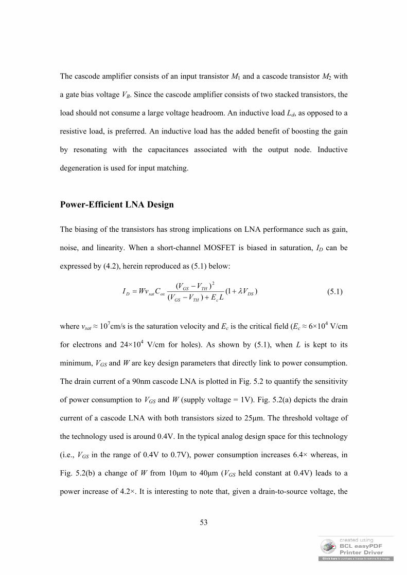
minimum, VGS and W are key design parameters that directly link to power consumption.
The drain current of a 90nm cascode LNA is plotted in Fig. 5.2 to quantify the sensitivity
of power consumption to VGS and W (supply voltage = 1V). Fig. 5.2(a) depicts the drain
current of a cascode LNA with both transistors sized to 25μm. The threshold voltage of
the technology used is around 0.4V. In the typical analog design space for this technology
(i.e., VGS in the range of 0.4V to 0.7V), power consumption increases 6.4× whereas, in
Fig. 5.2(b) a change of W from 10μm to 40μm (VGS held constant at 0.4V) leads to a
power increase of 4.2×. It is interesting to note that, given a drain-to-source voltage, the

54
performance of the MOSFET is strongly tied to the drain current density ID/W, which is
mainly controlled by VGS. The following subsections describe the sensitivity of gain,
noise, and linearity to VGS and W.
0
1000
2000
3000
4000
5000
6000
7000
0.3 0.4 0.5 0.6 0.70
200
400
600
800
1000
1200
1400
1600
10 15 20 25 30 35 40
I D[μA]
(a) (b)
Figure 5.2 ID of a cascode LNA. (a) ID vs. VGS (W1=W2=25μm), (b) ID vs. W (VGS=0.4V).
Gain
In conventional RF and microwave design approaches [26], [27], primarily developed for
high-speed bipolar circuits, fT is an indispensable design parameter. For CMOS
technologies, there is a characteristic current density associated with operating in strong
inversion that yields an optimal fT [6]. For the 90nm CMOS technology used in this work,
VGS ≈ 0.7V is required to reach the optimal value.

55
18
19
20
21
22
23
24
25
0.3 0.4 0.5 0.6 0.7
18
19
20
21
22
23
24
25
10 15 20 25 30 35 40
(a) (b)
Figure 5.3 Voltage gain of a cascode LNA. (a) Av vs. VGS, (b) Av. vs. W.
Figure 5.3(a) shows the simulated voltage gain Av of the cascode amplifier depicted in
Fig. 5.1 at 2.4GHz. While sweeping VGS, VB is also modified such that the ratio VGS1/VGS2,
hence gm1/gm2, is relatively constant. It may seem counterintuitive that Av only increases
slightly as VGS changes from 0.4V to 0.7V, which corresponds to roughly doubling fT and
gm1. The reason lies in the fact that the operating frequency is sufficiently low compared
to the maximum fT of the technology and therefore the benefits of increasing fT are not as
pronounced. This suggests that the use of fT as a design tool may have less influence in
modern RF design. In addition, as VGS increases, ID also increases, which reduces the
overall output impedance of the cascode structure. Since gain is the product of output
impedance and transconductance, the reduction of output impedance partially counteracts
the effects of increasing gm1 on the overall gain. For comparison, Fig. 5.3(b) shows
moderate increase in Av as the widths of both transistors are increased.

56
Noise
1
2
3
4
5
6
7
8
9
10
1 1.5 2 2.5 3 3.5
VGS
0.3V
VGS0.4V
VGS0.5V
VGS0.6V
VGS0.7V
(a)
1
2
3
4
5
6
7
8
9
10
1 1.5 2 2.5 3 3.5
(b)
Figure 5.4 NF of a cascode LNA. (a) NF vs. VGS, and (b) NF vs. W.
As discussed in Chapter 4, there is currently no robust noise optimization technique
specifically developed for the sub-mW regime. In the absence of such a technique, an
alternative design approach is to use the knowledge gained in Chapter 4 to establish an
initial biasing point and determine the sensitivity of NF with respect to VGS and W. For
this purpose, a 90nm cascode LNA is simulated. Fig. 5.4(a) shows NF as VGS of M1 is

57
swept from 0.3V to 0.7V (W = 25μm). VB is adjusted accordingly as mentioned earlier.
As can be seen from Fig. 5.4(a), NF is inadequate when operating in the subthreshold
region (VGS = 0.3V). For a change of VGS from 0.4V to 0.7V, NF is reduced by 0.6dB at
the expense of a 6.4× increase in the power consumption. Fig. 5.4(b) shows NF as the
width of both transistors are changed simultaneously from 10μm to 40μm (VGS = 0.4V),
which results in a 3.4dB NF improvement at the expense of 4.2× the power consumption.
This suggests that increasing W is a more effective method for reducing NF.
It is also instructive to use the SpectreRF simulator to obtain a noise summary that shows
the noise contribution of components. Fig. 5.5 depicts the RF signal source and the LNA
with the inductor models explicitly shown. The noise contributions from inductor
parasitic resistances are significant, suggesting high-Q inductors are highly desirable.
Figure 5.5 Noise contribution of the signal source and LNA components.

58
Linearity
As discussed in Chapter 2, there are two types of linearity performance for an LNA,
which are characterized by the input-referred 3rd-order intermodulation intercept point
(IIP3) and the input-referred 1dB voltage compression point (P1dB).
-4
-2
0
2
4
6
8
0.4 0.45 0.5 0.55 0.6 0.65 0.7
Figure 5.6 IIP3 vs. VGS of the cascode LNA.
-14
-13
-12
-11
-10
-9
-8
-7
-6
-5
0.3 0.4 0.5 0.6 0.7
Figure 5.7 P1dB vs. VGS of the cascode LNA.
Figure 5.6 and Fig. 5.7, respectively, show the IIP3 and P1dB of the cascode LNA with
25μm transistors. Since linearity is a function of gain, Fig. 5.6 and Fig. 5.7 also show the

59
linearity of the LNA with gate widths adjusted to maintain a constant gain across VGS. VB
is adjusted accordingly as mentioned earlier. Two observations can be made. First, IIP3
of the LNA is indeed the highest in moderate inversion, suggesting that the VIP3 peak
can be exploited in amplifier design. Second, the IIP3 and P1dB of the LNA degrade as
VGS increases. This is an interesting observation since previous analysis and
measurements reveal that the MOSFET IIP3 performance improves as VGS increases [9],
[10]. Lastly, it has been reported that linearity of a MOSFET in moderate inversion is not
well studied [9] and that the IIP3 peaking for a CMOS short-channel transistor may not
be easily applicable for RF LNA designs [10]. This is due to the fact that source
degeneration tends to improve the overall linearity but dampen the peak.
Simulation Results
The cascode LNA has been simulated using the BSIM3v3 model provided for the ST
Microelectronics 90nm CMOS process. On-chip inductors are modeled and designed
using the ASITIC electromagnetic field solver. Fig. 5.8 depicts the π-model for a 5nH
spiral inductor used as Lg and Ld in Fig. 5.1, implemented using the thick metal layer of a
90nm technology. This inductor has a Q of 7.3. To further improve Q, two metal layers
can be used to reduce the series resistance of the inductor. Ls is modeled similarly.
Figure 5.8 π-model of a 5nH spiral inductor.

60
In this design, Cm and Ctune are assumed to be implemented using high-Q metal-insulator-
metal (MIM) capacitors. The widths of both transistors are sized equally. VGS is chosen to
be 0.4V, slightly above the threshold voltage to exploit the high gm/ID in moderate
inversion. Table 1 is a summary of component values.
TABLE 1SUMMARY OF LNA COMPONENT VALUES
VDD (V) 1Lg = Ld (nH) 5Ls (nH) 2Cm (fF) 480Ctune (fF) 720W1/L1 (μm) 25/0.1W2/L2 (μm) 25/0.1Vin,DC (V) 0.4VB (V) 0.9
Figure 5.9 shows the voltage gain Av and NF of the LNA. The voltage gain is 22.7dB in
the 2.4GHz band with a 3dB bandwidth of around 300MHz.
0
5
10
15
20
25
1.5 2 2.5 3 3.5
2.5
3
3.5
4
4.5
5
Figure 5.9 Gain and NF of the proposed LNA.

61
As depicted in Fig. 5.10, an S11 of −14.7dB provides a good input impedance matching to
50Ω. NF is 2.8dB which is acceptable for short-range applications. IIP3 and P1dB are
+5.14dBm and −10dBm, respectively. Table 2 summarizes the performance of the LNA.
The circuit consumes 943μW from a 1V supply.
-25
-20
-15
-10
-5
0
1.5 2 2.5 3 3.5
S11
[dB
]
Figure 5.10 S11 of the proposed LNA.
TABLE 2SUMMARY OF LNA PERFORMANCE
Gain (dB) 22.7NF (dB) 2.8S11 (dB) −14.7IIP3 (dBm) 5.14P1dB (dBm) −10PDC (μW) 943fc (GHz) 2.4Gate L (μm) 0.09

62
Performance Summary
Table 3 shows a performance comparison between the proposed LNA and low-power
CMOS LNAs from recent literature. The performance comparison is further illustrated on
the gain-power design space as in Fig. 5.11.
TABLE 3COMPARISON OF CMOS LOW-POWER LNAS
This work [3]1,# [28]2,# [2]# [29]# [30]# [31]3,# [32]# [33]#
Gain (dB) 22.7 13.6 13* 12 9.2* 11.5 10.1 12.8 19NF (dB) 2.8 4.6 3.6 1.8 3.6 3.4 2.9 1.4 2.8S11 (dB) −14.7 −5 <−10 −18 −10 -14 −10.1 − −14.5IIP3 (dBm) 5.14 7.2 −10 −3 −7.25 − +4 +13.3 −P1dB (dBm) −10 −0.2 – – −15.8 −8 −7 − −PDC (mW) 0.94 0.26 0.72 0.9 1 4 11.7 14.4 15fc (GHz) 2.4 1 0~0.96 2.4 5.5 5.7 2.4 2.0 2.4Gate L (μm) 0.09 0.18 0.13 0.18 0.09 0.18 0.18 0.18 0.18* Power gain, 1 Subthreshold design, 2 UWB design, 3 Dual-band design, # Measurement
30
25
20
15
10
5
0
0 1 2 3 4 5
Noise Figure (dB)
Gai
n (d
B)
< 1mW
> 1mW
This Thesis
[3], ‘05[28], ‘06[2], ‘05
[29], ‘04
[30], ‘06[32], ‘06
[31], ‘05
[33], ‘05
Best
Worse
Figure 5.11 Graphical illustration comparing recently published LNAs and this work.

63
A direct comparison of LNAs listed in Table 3 is a challenge as most LNAs have
specifications that are tailored to work with the specific radio architecture and application.
An attempt is made to compare the proposed LNA to comparable low-power, relatively
narrow-band LNAs. There are several aspects to note in this comparison. First, the
proposed work is based on simulation results and the others are based on measurements.
When a chip is fabricated, its performance tends to degrade due to unaccounted parasitics
and the assumptions made during circuit design. Second, not all the LNAs compared
operate at the same frequency. Typically, more power is required to provide gain at a
higher frequency, for example, the LNAs in [3] and [28] have lower power consumption.
Third, all LNAs use the cascode topology or its variants, except for the ones in [3] and
[28]. The LNA in [3] uses a common-source topology, which exploits the relatively high
MOSFET output resistance in 0.18μm CMOS. This LNA design may have difficulty
delivering gain when ported to the 90nm technology. Also, the fact that it is targeted for
lower frequency operation enables a subthreshold design, giving it an advantage in
transconductance efficiency over other LNAs. The LNA in [28] uses the common-gate
topology as it needs to provide a large bandwidth for the targeted ultra-wideband
application. Since this design and the dual-band LNA in [31] need to cover a greater
bandwidth, a higher power consumption and a lower gain is inevitable. Fourth, the LNA
in [32] employs an extra transistor for post-linearization, which results in larger power
consumption but the best linearity in the comparison. From Fig. 5.11, it can be seen that
the LNA designed based on the proposed approach demonstrates a competitive gain and
noise figure amongst low-power LNAs.

64
Chapter 6Conclusions and Future Works
Conclusion
In this thesis, a design methodology for low-power CMOS RF inductively degenerated
LNAs has been introduced. The design approach presented in this dissertation differs
from existing techniques in that it begins with determining how device biasing affects
gain, noise, linearity, and power consumption of the amplifier to ensure a well-rounded
design. Design plots have been used to help the circuit designer in understanding the
fundamental characteristics of the MOSFET in preparation to applying the design
methodology. To demonstrate the technique, a fully integrated RF CMOS LNA is design
and simulated. This 2.4GHz 90nm cascode LNA achieves a voltage gain of 22.7dB, NF
of 2.8dB, IIP3 of +5.14dBm, and P1dB of −10dBm, while consuming 943μW from a 1V
supply. This study has revealed that for designs that operate well below fT, a balanced
design can be achieved by biasing the device just above the threshold voltage to exploit
the high gm/ID. This achieves low power consumption while avoiding the performance
degradation associated with the subthreshold region. This observation is significant as
many RF circuits for applications operating in the low-GHz range implemented in a
modern CMOS technology can be designed based on the proposed technique.

65
Future Work
Although this work has provided solutions to the challenges of power-efficient design, it
has also uncovered many interesting topics worthy of further investigation. They often
require a deeper understanding and characterization of the device and are listed as
follows:
1) Conventional power-constrained noise optimization methods proposed to target low-
power design have their limits. The techniques is based on first finding an optimal gate
width, then biasing the device with the amount of drain current allowed by the power
constraint. In sub-mW designs, the large optimal gate width combined with a small drain
current often force the device to be biased in the subthreshold region. When subthreshold
operation is inadequate, such as insufficient frequency response, the technique is no
longer applicable. An effective noise optimization technique for the ultra-low-power
design space is needed.
2) The proposed design methodology has been devised with a focus of maximizing
transconductance efficiency, which translates to power-efficient amplifier designs.
Although current low-power applications tend to have a more relaxed noise requirement,
it is worthwhile to incorporate noise formulation into the transconductance efficiency
framework so that the establishment of biasing condition can include a quantitative noise
analysis.

66
3) The effectiveness of the proposed design methodology has thus far been verified with
SpectreRF simulations. Silicon implementation is the next logical step to confirm
simulation results.
4) There is only a narrow range of biasing conditions that can exploit the high MOSFET
linearity performance in moderate inversion. This narrow range demands for accurate
biasing circuits; therefore, conventional LNA designs have not exploited this effect.
Biasing circuits with improved accuracy may make the use of the high MOSFET linearity
performance possible and reliable.
5) On-chip inductors are area intensive and do not scale well with technology. They are
of low quality factor and contribute substantially to the noise figure of the amplifier.
Improved on-chip implementation is needed.
6) Process variation is expected to increase as CMOS technology scales. Advanced
layout techniques and robust calibration schemes for mitigating process variation is
needed.
There is much work to be done in the area of low power, deep submicron CMOS LNA
design. The landscape of analog circuit design is rapidly changing as technology scales to
quantum levels, opening the designer to a new world of challenges and possibilities.

67
References
[1] D.Shaeffer and T. Lee, “A 1.5V, 1.5 GHz CMOS low noise amplifier,” IEEE J. Solid State Circuits, vol. 32, May 1997.
[2] T.-K. Nguyen, S.-K. Han, and S.-G. Lee, “Ultra-low-power 2.4GHz image-rejection low-noise amplifier,” Electronics Letters, vol. 41, no. 15, July 2005.
[3] D. B. G. Perumana, S. Chakraborty, C.-H. Lee, and J. Laskar, “A fully monolithic 260-μW, 1-GHz subthreshold low noise amplifier,” IEEE Microwave and Wireless Components Letters, vol. 15, no. 6, Jun 2005.
[4] W. Kluge, F. Poegel, H. Roller, M. Lange, T. Ferchland, L. Dathe, and D. Eggert, “A fully integrated 2.4-GHz IEEE 802.15.4-compliant transceiver for ZigBeeTM
applications,” IEEE J. Solid-State Circuits, vol. 41, no. 12, Dec 2006.
[5] T.-K. Nguyen, C. H. Kim, G. J. Ihm, M. S. Yang, and S.-G. Lee, “CMOS Low-noise amplifier design optimization techniques,” IEEE Trans. on Microwave Theory and Techniques, vol. 52, no. 5, May 2004.
[6] T. O. Dickson, K. Yau, T. Chalvatzis, A. M. Mangan, E. Laskin, R. Beerkens, P. Westergaard, M. Tazlauanu, M-T Yang, and S. P. Voinigescu, “The invariance of characteristic current densities in nanoscale MOSFETs and its impact on algorithmic design methodologies and design porting of Si(Ge) (Bi)CMOS high-speed building blocks,” IEEE J. Solid-State Circuits, vol. 41, no. 8, Aug. 2006.
[7] B. Murmann, P. Nikaeen, D. J. Connelly, and R. W. Dutton, “Impact of scaling on analog performance and associated modeling needs,” IEEE Transactions on Electron Devices, vol. 53, no. 9, Sep. 2006.
[8] P. H.Woerlee, M. J. Knitel, R. van Langevelde, D. B. M. Klaassen, L. F. Tiemeijer, A. J. Scholten, and A. T. A. Zegers-van Duijnhoven, “RF-CMOS performance trends,” IEEE Trans. Electron Devices, vol. 48, no. 8, Aug. 2001.
[9] B. Toole, C. Plett, and M. Cloutier, “RF circuit implications of moderate inversion enhanced linear region in MOSFETs,” IEEE Trans. Circuits and Systems I, vol. 51, no. 2, Feb. 2004.
[10] R.A. Baki, T. K. K. Tsang, and M. N. El-Gamal, “Distortion in RF CMOS short-channel low-noise amplifiers,” IEEE Trans. Microwave Theory and Techniques, vol. 54, no. 1, Jan. 2006.
[11] P. Gray, P. Hurst, S. Lewis, R. Meyer, Analysis and Design of Analog Integrated Circuits, 4th Edition, John Wiley & Sons, New York, 2001.

68
[12] R. Lu, “CMOS low noise amplifier design for wireless sensor networks,” Master of Science Thesis, UC Berkeley, 2003.
[13] T. Lee, The Design of CMOS Radio-Frequency Integrated Circuits, Cambridge University Press, Cambridge, UK, 1998.
[14] G. Gonzalez, Microwave Transistor Amplifiers: Analysis and Design, 2nd Edition, Prentice Hall, 1996.
[15] J-S. Goo, “High frequency noise in CMOS low noise amplifiers,” Doctor of Philosophy Thesis, Stanford, 2001.
[16] J. Rollett, “Stability and power-gain invariants of linear twoports,” IRE Trans. on Circuit Theory, vol. 9, issue 1, Mar. 1962.
[17] A. Van Der Ziel, Noise in solid state devices and circuits, Wiley, New York, 1996.
[18] A. Abidi, “High frequency noise measurements on FETs with small dimensions,” IEEE Trans. on Electronic Devices, vol. 33, Nov. 1986, pp. 1801 – 1805.
[19] W. Zhuo, X. Li, S. Shekhar, S. H. K. Embabi, J. Pineda de Gyvez, D. J. Allstot, and E. Sanchez-Sinencio, “A capacitor cross-coupled common-gate low-noise amplifier,” IEEE Trans. on Circuits and Systems II, vol. 52, no. 12, Dec. 2005.
[20] F. Zhang and P. R. Kinget, “Low-power programmable gain CMOS distributed LNA,” IEEE J. Solid-State Circuits, vol. 41, no. 6, Jun. 2006.
[21] J. Janssens and M. Steyaert, CMOS cellular receiver front-ends, Klewer, The Netherlands, 2002.
[22] Ming Cai, “Design studies of nanometer-gate low-noise amplifier near the limits of CMOS scaling,” Doctor of Philosophy Thesis, University of California, San Diego, San Diego, CA, 2006.
[23] A. Niknejad, “Analysis, simulation, and applications of passive devices on conductive substrates,” Doctor of Philosophy Thesis, University of California, Berkeley, Berkeley, CA, 2000.
[24] A. M. Niknejad and R. G. Meyer, “Analysis, design, and optimization of spiral inductors and transformers for Si RF IC’s,” IEEE J. Solid-State Circuits, vol. 33, no. 10, Oct. 1998.
[25] B. Razavi, RF microelectronics, Prentice Hall, Upper Saddle River, NJ, 1998.

69
[26] H.-M. Rein and M. Moller, “Design considerations for very-high-speed Si-bipolar IC’s operating up to 50 Gb/s,” IEEE J. Solid-State Circuits, vol. 31, no. 8, Aug. 1996.
[27] G. A. M. Hurkx, “The relevance of fT and fMAX for the speed of a bipolar CE amplifier stage,” IEEE. Trans. Electron Devices, vol. 44, no. 5, May 1997.
[28] S. B. T. Wang, A. M. Niknejad, and R. W. Brodersen, “Design of a sub-mW 960-MHz UWB CMOS LNA,” IEEE J. Solid-State Circuits, vol. 41, no. 11, Nov. 2006.
[29] D. Linten, L. Aspemyr, W. Jeamsaksiri, J. Ramos, A. Mercha, S. Jenei, S. Thijs, R. Garcia, H. Jacobsson, P. Wambacq, S. Donnay, and S. Decoutere, “Low-power 5 GHz LNA and VCO in 90nm RF CMOS,” IEEE Sym. on VLSI Circuits, June 2004.
[30] S. Asgaran, M. J. Deen, and C.-H. Chen, “A 4-mW monolithic CMOS LNA at 5.7GHz with the gate resistance used for input matching,” IEEE Microwave and Wireless Components Letters, vol. 16, no. 4, Apr. 2006.
[31] L.-H. Lu, H.-H. Hsieh, and Y.-S. Wang, “A compact 2.4/5.2-GHz CMOS dual-band low-noise amplifier,” IEEE Microwave and Wireless Components Letters, vol. 15, no. 10, Oct. 2005.
[32] T.-S. Kim and B.-S. Kim, “Post-linearization of cascode CMOS low noise amplifier using folded PMOS IMD sinker,” IEEE Microwave and Wireless Component Letters, vol. 16, no. 4, Apr. 2006.
[33] M. Shouxian, M. Jian-Guo, Y. K. Seng, and D. M. Anh, “A modified architecture used for input matching in CMOS low-noise amplifiers,” IEEE Trans. on Circuits and Systems II, vol. 52, no. 11, Nov. 2005.