designing efficient network interfaces for system …designing efficient network interfaces for...
TRANSCRIPT
r
Designing Efficient Network Interfaces FoSystem Area NetworksInauguraldissertation
zur Erlangung des akademischen Grades
eines Doktors der Naturwissenschaften
der Universität Mannheim
vorgelegt von
Dipl.-Inf. Lars Rzymianowicz
aus Rendsburg
Mannheim, 2002

Dekan: Professor Dr. Herbert Popp, Universität Mannheim Referent: Professor Dr. Ulrich Brüning, Universität Mannheim Korreferent: Professor Dr. Volker Lindenstruth, Universität Heidelberg Tag der mündlichen Prüfung: 28. August 2002

r
Designing Efficient Network Interfaces FoSystem Area NetworksInauguraldissertation
zur Erlangung des akademischen Grades
eines Doktors der Naturwissenschaften
der Universität Mannheim
vorgelegt von
Dipl.-Inf. Lars Rzymianowicz
aus Rendsburg
Mannheim, 2002


r
nce,
ystem
too
too
the
er-
other
ct for
ized
ver-
es-
sical
ars,
SAN
ith the
net-
nter-
SMP
hould
hip,
on-
ip”
Abstract
Designing Efficient Network Interfaces FoSystem Area Networks
by
Lars Rzymianowicz
Universität Mannheim
The network is the key component of a Cluster of Workstations/PCs. Its performa
measured in terms of bandwidth and latency, has a great impact on the overall s
performance. It quickly became clear that traditional WAN/LAN technology is not
well suited for interconnecting powerful nodes into a cluster. Their poor performance
often slows down communication-intensive applications. This observation led to
birth of a new class of networks called System Area Networks (SAN).
But still SANs like Myrinet, SCI or ServerNet do not deliver an appropriate level of p
formance. Some are hampered by the fact, that they were originally targeted at an
field of application. E.g. SCI was intended to serve as a cache-coherent interconne
fine-grain communication between tightly coupled nodes. Its architecture is optim
for this area and behaves less optimal for bandwidth-hungry applications. Earlier
sions of Myrinet suffered from slow versions of their proprietary LANai network proc
sor and slow on-board SRAM. And even though a standard I/O bus with a phy
bandwidth of more then 500 Mbyte/s (PCI 64 bit/66 MHz) has been available for ye
typical SANs only offer between 100-200 Mbyte/s.
All the disadvantages of current implementations lead to the idea to develop a new
capable of delivering the performance needed by todays clusters and to keep up w
fast progress in CPU and memory performance. It should completely remove the
work as communication bottleneck and support efficient methods for host-network i
action. Furthermore, it should be ideally suited for use in small-scale (2-8 CPUs)
nodes, which are used more and more as cluster nodes. And last but not least, it s
be a cost-efficient implementation.
All these requirements guided the specification of the ATOLL network. On a single c
not one but four network interfaces (NI) have been implemented, together with an
chip 4x4 full-duplex switch and four link interfaces. This unique “Network on a Ch
V

s are
s the
nks
ts of
pro-
s at
I-X
bina-
ffers
de
ed for
sage
been
an
rk is
cific
ifica-
it
the
est
a die
ous
CI-
the
. All
for
oduc-
eeks
by a
ntest
mier
architecture is best suited for interconnecting SMP nodes, where multiple CPU
given an exclusive NI and do not have to share a single interface. It also remove
need for any additional switching hardware, since the four byte-wide full-duplex li
can be connected by cables with neighbor nodes in an arbitrary network topology.
Despite its complexity and size, the whole network interface card (NIC) only consis
a single chip and 4 cable connectors, a very cost-efficient architecture. Each link
vides 250 Mbyte/s in one direction, offering a total bisection bandwidth of 2 Gbyte/
the network side. The next generation of I/O bus technology, a 64 bit/133 MHz PC
bus interface, has been integrated to make use of this high bandwidth. A novel com
tion of different data transfer methods has been implemented. Each of the four NIs o
transfer via Direct Memory Access (DMA) or Programmed I/O (PIO). The PIO mo
eliminates any need for an intermediate copy of message data and is ideally suit
fine-grain communication, whereas the DMA mode is best suited for larger mes
sizes. In addition, new techniques for event notification and error correction have
included in the ATOLL NI. Intensive simulations show that the ATOLL architecture c
deliver the performance expected. For the first time in Cluster Computing, the netwo
no more the communication bottleneck.
Specifying such a complex design is one task, implementing it in an Application Spe
Integrated Circuit (ASIC) is an even greater challenge. From implementing the spec
tion in a Register/Transfer-Level (RTL) module to the final VLSI layout generation
took almost three years. Implemented in a state-of-the-art IC technology with
CMOS-Digital 0.18 um process of UMC, Taiwan, the ATOLL chip is one of the fast
and most complex ASICs ever designed outside the commercial IC industry. With
size of 5.8x5.8 sqmm, 43 on-chip SRAM blocks with 100 kbit total, 6 asynchron
clock domains (133-250 MHz), one large PCI-X IP cell and full-custom LVDS and P
X I/O cells, a carefully planned design flow had to be followed. Only the design of
full-custom I/Os and the Place & Route of the layout were done by external partners
the rest of the design flow, from RTL coding to simulation, from synthesis to design
test, was done by ourselves. Finally, the completed layout was given to sample pr
tion in February 2002, first engineering samples are expected to be delivered 10 w
later.
The ATOLL ASIC is one of the most complex and fastest chips ever implemented
European university. Recently, the design has won the third place in the design co
organized at the Design, Automation & Test in Europe (DATE) conference, the pre
European event for electronic design.
VI

. .1
.
. . .
. .
11
. . . .15
. . .24
Table of Contents
CHAPTER 1 Introduction . . . . . . . . . . . . . . . . . . . . . . . . . . . . . . . . . . . . . . . . . . . .
1.1 Cluster Computing . . . . . . . . . . . . . . . . . . . . . . . . . . . . . . . . . . . . . . . . . . . . . . . . . . . . . . . . . . . . . .1
1.1.1 Trends . . . . . . . . . . . . . . . . . . . . . . . . . . . . . . . . . . . . . . . . . . . . . . . . . . . . . . . . . . . . . . . . . . . . .2
1.1.2 Managing large installations . . . . . . . . . . . . . . . . . . . . . . . . . . . . . . . . . . . . . . . . . . . . . . . . . . . .3
1.1.3 Driving factors and future directions . . . . . . . . . . . . . . . . . . . . . . . . . . . . . . . . . . . . . . . . . . . .3
1.2 System Area Networks . . . . . . . . . . . . . . . . . . . . . . . . . . . . . . . . . . . . . . . . . . . . . . . . . . . . . . . . . . .4
1.2.1 The need for a new class of networks . . . . . . . . . . . . . . . . . . . . . . . . . . . . . . . . . . . . . . . . . .4
1.2.2 Emerging from existing technology . . . . . . . . . . . . . . . . . . . . . . . . . . . . . . . . . . . . . . . . . .. .5
1.3 ASIC Design . . . . . . . . . . . . . . . . . . . . . . . . . . . . . . . . . . . . . . . . . . . . . . . . . . . . . . . . . . . . . . . . . . .5
1.3.1 Using 10+ million transistors . . . . . . . . . . . . . . . . . . . . . . . . . . . . . . . . . . . . . . . . . . . . . . . . . . .6
1.3.2 Timing closure . . . . . . . . . . . . . . . . . . . . . . . . . . . . . . . . . . . . . . . . . . . . . . . . . . . . . . . . . . . . . .6
1.3.3 Power dissipation . . . . . . . . . . . . . . . . . . . . . . . . . . . . . . . . . . . . . . . . . . . . . . . . . . . . . . . . . . . .7
1.3.4 Verification bottleneck . . . . . . . . . . . . . . . . . . . . . . . . . . . . . . . . . . . . . . . . . . . . . . . . . . . . . . . .9
1.4 Contributions. . . . . . . . . . . . . . . . . . . . . . . . . . . . . . . . . . . . . . . . . . . . . . . . . . . . . . . . . . . . . . . . . . .9
1.5 Organization . . . . . . . . . . . . . . . . . . . . . . . . . . . . . . . . . . . . . . . . . . . . . . . . . . . . . . . . . . . . . . . . . .10
CHAPTER 2 System Area Networks . . . . . . . . . . . . . . . . . . . . . . . . . . . . . . . . . . . .
2.1 Wide/Local Area Networks . . . . . . . . . . . . . . . . . . . . . . . . . . . . . . . . . . . . . . . . . . . . . . . . . . . . . .11
2.1.1 User-level message layers . . . . . . . . . . . . . . . . . . . . . . . . . . . . . . . . . . . . . . . . . . . . . . . . . . . . .11
2.2 Design goals . . . . . . . . . . . . . . . . . . . . . . . . . . . . . . . . . . . . . . . . . . . . . . . . . . . . . . . . . . . . . . . . . .13
2.2.1 Price versus performance . . . . . . . . . . . . . . . . . . . . . . . . . . . . . . . . . . . . . . . . . . . . . . . . . . . . .13
2.2.2 Scalability . . . . . . . . . . . . . . . . . . . . . . . . . . . . . . . . . . . . . . . . . . . . . . . . . . . . . . . . . . . . . . . . .13
2.2.3 Reliability . . . . . . . . . . . . . . . . . . . . . . . . . . . . . . . . . . . . . . . . . . . . . . . . . . . . . . . . . . . . . . . . .14
2.3 General architecture . . . . . . . . . . . . . . . . . . . . . . . . . . . . . . . . . . . . . . . . . . . . . . . . . . . . . . . . . . . .14
2.3.1 Shared memory vs. distributed memory . . . . . . . . . . . . . . . . . . . . . . . . . . . . . . . . . . . . . .
2.3.2 NI location. . . . . . . . . . . . . . . . . . . . . . . . . . . . . . . . . . . . . . . . . . . . . . . . . . . . . . . . . . . . . . . . .16
2.4 Design details . . . . . . . . . . . . . . . . . . . . . . . . . . . . . . . . . . . . . . . . . . . . . . . . . . . . . . . . . . . . . . . . .18
2.4.1 Physical layer . . . . . . . . . . . . . . . . . . . . . . . . . . . . . . . . . . . . . . . . . . . . . . . . . . . . . . . . . . . . . .19
2.4.2 Switching. . . . . . . . . . . . . . . . . . . . . . . . . . . . . . . . . . . . . . . . . . . . . . . . . . . . . . . . . . . . . . . . . .20
2.4.3 Routing . . . . . . . . . . . . . . . . . . . . . . . . . . . . . . . . . . . . . . . . . . . . . . . . . . . . . . . . . . . . . . . . . . .21
2.4.4 Flow control . . . . . . . . . . . . . . . . . . . . . . . . . . . . . . . . . . . . . . . . . . . . . . . . . . . . . . . . . . . . . . .23
2.4.5 Error detection and correction. . . . . . . . . . . . . . . . . . . . . . . . . . . . . . . . . . . . . . . . . . . . . . . . . .23
2.5 Data transfer . . . . . . . . . . . . . . . . . . . . . . . . . . . . . . . . . . . . . . . . . . . . . . . . . . . . . . . . . . . . . . . . . .24
2.5.1 Programmed I/O versus Direct Memory Access . . . . . . . . . . . . . . . . . . . . . . . . . . . . . . . .
2.5.2 Control transfer . . . . . . . . . . . . . . . . . . . . . . . . . . . . . . . . . . . . . . . . . . . . . . . . . . . . . . . . . . . . .26
2.5.3 Collective operations. . . . . . . . . . . . . . . . . . . . . . . . . . . . . . . . . . . . . . . . . . . . . . . . . . . . . . . . .26
2.6 SCI . . . . . . . . . . . . . . . . . . . . . . . . . . . . . . . . . . . . . . . . . . . . . . . . . . . . . . . . . . . . . . . . . . . . . . . . .26
2.6.1 Targeting DSM systems . . . . . . . . . . . . . . . . . . . . . . . . . . . . . . . . . . . . . . . . . . . . . . . . . . . . . .27
2.6.2 The Dolphin SCI adapter . . . . . . . . . . . . . . . . . . . . . . . . . . . . . . . . . . . . . . . . . . . . . . . . . . . . .28
2.6.3 Remarks. . . . . . . . . . . . . . . . . . . . . . . . . . . . . . . . . . . . . . . . . . . . . . . . . . . . . . . . . . . . . . . . . . .29
2.7 ServerNet . . . . . . . . . . . . . . . . . . . . . . . . . . . . . . . . . . . . . . . . . . . . . . . . . . . . . . . . . . . . . . . . . . . .30
2.7.1 Scalability and reliability . . . . . . . . . . . . . . . . . . . . . . . . . . . . . . . . . . . . . . . . . . . . . . . . . . . . .30
2.7.2 Link technology . . . . . . . . . . . . . . . . . . . . . . . . . . . . . . . . . . . . . . . . . . . . . . . . . . . . . . . . . . . .31
VII

.
. . . .39
1
.
. .
. . .87
2.7.3 Data transfer . . . . . . . . . . . . . . . . . . . . . . . . . . . . . . . . . . . . . . . . . . . . . . . . . . . . . . . . . . . . . . .32
2.7.4 Switches . . . . . . . . . . . . . . . . . . . . . . . . . . . . . . . . . . . . . . . . . . . . . . . . . . . . . . . . . . . . . . . . . .32
2.7.5 Software . . . . . . . . . . . . . . . . . . . . . . . . . . . . . . . . . . . . . . . . . . . . . . . . . . . . . . . . . . . . . . . . . .33
2.7.6 Remarks. . . . . . . . . . . . . . . . . . . . . . . . . . . . . . . . . . . . . . . . . . . . . . . . . . . . . . . . . . . . . . . . . . .33
2.8 Myrinet . . . . . . . . . . . . . . . . . . . . . . . . . . . . . . . . . . . . . . . . . . . . . . . . . . . . . . . . . . . . . . . . . . . . . .34
2.8.1 NIC architecture . . . . . . . . . . . . . . . . . . . . . . . . . . . . . . . . . . . . . . . . . . . . . . . . . . . . . . . . . . . .34
2.8.2 Transport layer and switches. . . . . . . . . . . . . . . . . . . . . . . . . . . . . . . . . . . . . . . . . . . . . . . . . . .35
2.8.3 Software and performance . . . . . . . . . . . . . . . . . . . . . . . . . . . . . . . . . . . . . . . . . . . . . . . . . . .36
2.8.4 Remarks. . . . . . . . . . . . . . . . . . . . . . . . . . . . . . . . . . . . . . . . . . . . . . . . . . . . . . . . . . . . . . . . . . .37
2.9 QsNet . . . . . . . . . . . . . . . . . . . . . . . . . . . . . . . . . . . . . . . . . . . . . . . . . . . . . . . . . . . . . . . . . . . . . . .38
2.9.1 NIC architecture . . . . . . . . . . . . . . . . . . . . . . . . . . . . . . . . . . . . . . . . . . . . . . . . . . . . . . . . . . . .38
2.9.2 Switches and topology . . . . . . . . . . . . . . . . . . . . . . . . . . . . . . . . . . . . . . . . . . . . . . . . . . . . . . .39
2.9.3 Programming interface and performance . . . . . . . . . . . . . . . . . . . . . . . . . . . . . . . . . . . . .
2.9.4 Remarks. . . . . . . . . . . . . . . . . . . . . . . . . . . . . . . . . . . . . . . . . . . . . . . . . . . . . . . . . . . . . . . . . . .41
2.10 IBM SP Switch2 . . . . . . . . . . . . . . . . . . . . . . . . . . . . . . . . . . . . . . . . . . . . . . . . . . . . . . . . . . . . . .41
2.10.1 NIC architecture . . . . . . . . . . . . . . . . . . . . . . . . . . . . . . . . . . . . . . . . . . . . . . . . . . . . . . . . . . .42
2.10.2 Network switches . . . . . . . . . . . . . . . . . . . . . . . . . . . . . . . . . . . . . . . . . . . . . . . . . . . . . . . . . .43
2.10.3 Remarks. . . . . . . . . . . . . . . . . . . . . . . . . . . . . . . . . . . . . . . . . . . . . . . . . . . . . . . . . . . . . . . . . .44
2.11 Infiniband . . . . . . . . . . . . . . . . . . . . . . . . . . . . . . . . . . . . . . . . . . . . . . . . . . . . . . . . . . . . . . . . . . .45
2.11.1 Architecture. . . . . . . . . . . . . . . . . . . . . . . . . . . . . . . . . . . . . . . . . . . . . . . . . . . . . . . . . . . . . . .45
2.11.2 Protocol stack . . . . . . . . . . . . . . . . . . . . . . . . . . . . . . . . . . . . . . . . . . . . . . . . . . . . . . . . . . . . .47
2.11.3 Remarks. . . . . . . . . . . . . . . . . . . . . . . . . . . . . . . . . . . . . . . . . . . . . . . . . . . . . . . . . . . . . . . . . .49
CHAPTER 3 The ATOLL System Area Network . . . . . . . . . . . . . . . . . . . . . . . . . .5
3.1 A new SAN architecture: ATOLL . . . . . . . . . . . . . . . . . . . . . . . . . . . . . . . . . . . . . . . . . . . . . . . .51
3.1.1 Design details of ATOLL . . . . . . . . . . . . . . . . . . . . . . . . . . . . . . . . . . . . . . . . . . . . . . . . . . . . .52
3.2 Top-level architecture . . . . . . . . . . . . . . . . . . . . . . . . . . . . . . . . . . . . . . . . . . . . . . . . . . . . . . . . . . .54
3.2.1 Address space layout. . . . . . . . . . . . . . . . . . . . . . . . . . . . . . . . . . . . . . . . . . . . . . . . . . . . . . . . .56
3.3 PCI-X interface . . . . . . . . . . . . . . . . . . . . . . . . . . . . . . . . . . . . . . . . . . . . . . . . . . . . . . . . . . . . . . . .58
3.4 Synchronization interface . . . . . . . . . . . . . . . . . . . . . . . . . . . . . . . . . . . . . . . . . . . . . . . . . . . . . . . .60
3.4.1 Completer interface. . . . . . . . . . . . . . . . . . . . . . . . . . . . . . . . . . . . . . . . . . . . . . . . . . . . . . . . . .61
3.4.2 Slave-Write data path . . . . . . . . . . . . . . . . . . . . . . . . . . . . . . . . . . . . . . . . . . . . . . . . . . . . . . . .63
3.4.3 Slave-Read data path. . . . . . . . . . . . . . . . . . . . . . . . . . . . . . . . . . . . . . . . . . . . . . . . . . . . . . . . .63
3.4.4 Master-Write data path . . . . . . . . . . . . . . . . . . . . . . . . . . . . . . . . . . . . . . . . . . . . . . . . . . . . . . .64
3.4.5 Master-Read data path. . . . . . . . . . . . . . . . . . . . . . . . . . . . . . . . . . . . . . . . . . . . . . . . . . . . . . . .65
3.4.6 Requester interface . . . . . . . . . . . . . . . . . . . . . . . . . . . . . . . . . . . . . . . . . . . . . . . . . . . . . . . . . .66
3.4.7 Device initialization . . . . . . . . . . . . . . . . . . . . . . . . . . . . . . . . . . . . . . . . . . . . . . . . . . . . . . . . .67
3.5 Port interconnect . . . . . . . . . . . . . . . . . . . . . . . . . . . . . . . . . . . . . . . . . . . . . . . . . . . . . . . . . . . . . . .70
3.5.1 ATOLL control and status registers . . . . . . . . . . . . . . . . . . . . . . . . . . . . . . . . . . . . . . . . . . .71
3.6 Host port . . . . . . . . . . . . . . . . . . . . . . . . . . . . . . . . . . . . . . . . . . . . . . . . . . . . . . . . . . . . . . . . . . . . .81
3.6.1 Address layout. . . . . . . . . . . . . . . . . . . . . . . . . . . . . . . . . . . . . . . . . . . . . . . . . . . . . . . . . . . . . .82
3.6.2 PIO-send unit . . . . . . . . . . . . . . . . . . . . . . . . . . . . . . . . . . . . . . . . . . . . . . . . . . . . . . . . . . . . . .83
3.6.3 PIO-receive unit . . . . . . . . . . . . . . . . . . . . . . . . . . . . . . . . . . . . . . . . . . . . . . . . . . . . . . . . . . . .85
3.6.4 Data structures for DMA-based communication . . . . . . . . . . . . . . . . . . . . . . . . . . . . . . . .
3.6.5 Status/control registers . . . . . . . . . . . . . . . . . . . . . . . . . . . . . . . . . . . . . . . . . . . . . . . . . . . . . . .89
3.6.6 DMA-send unit . . . . . . . . . . . . . . . . . . . . . . . . . . . . . . . . . . . . . . . . . . . . . . . . . . . . . . . . . . . . .91
3.6.7 DMA-receive unit . . . . . . . . . . . . . . . . . . . . . . . . . . . . . . . . . . . . . . . . . . . . . . . . . . . . . . . . . . .93
VIII

. .
07
29
137
. . . i
. . iii
3.6.8 Replicator . . . . . . . . . . . . . . . . . . . . . . . . . . . . . . . . . . . . . . . . . . . . . . . . . . . . . . . . . . . . . . . . .94
3.7 Network port . . . . . . . . . . . . . . . . . . . . . . . . . . . . . . . . . . . . . . . . . . . . . . . . . . . . . . . . . . . . . . . . . .96
3.7.1 Message frames and link protocol. . . . . . . . . . . . . . . . . . . . . . . . . . . . . . . . . . . . . . . . . . . . .96
3.7.2 Send path. . . . . . . . . . . . . . . . . . . . . . . . . . . . . . . . . . . . . . . . . . . . . . . . . . . . . . . . . . . . . . . . . .97
3.7.3 Receive path . . . . . . . . . . . . . . . . . . . . . . . . . . . . . . . . . . . . . . . . . . . . . . . . . . . . . . . . . . . . . . .98
3.8 Crossbar . . . . . . . . . . . . . . . . . . . . . . . . . . . . . . . . . . . . . . . . . . . . . . . . . . . . . . . . . . . . . . . . . . . . .99
3.9 Link port . . . . . . . . . . . . . . . . . . . . . . . . . . . . . . . . . . . . . . . . . . . . . . . . . . . . . . . . . . . . . . . . . . . .101
3.9.1 Link protocol. . . . . . . . . . . . . . . . . . . . . . . . . . . . . . . . . . . . . . . . . . . . . . . . . . . . . . . . . . . . . .101
3.9.2 Output port . . . . . . . . . . . . . . . . . . . . . . . . . . . . . . . . . . . . . . . . . . . . . . . . . . . . . . . . . . . . . . .103
3.9.3 Input port. . . . . . . . . . . . . . . . . . . . . . . . . . . . . . . . . . . . . . . . . . . . . . . . . . . . . . . . . . . . . . . . .105
CHAPTER 4 Implementation . . . . . . . . . . . . . . . . . . . . . . . . . . . . . . . . . . . . . . . . .1
4.1 Design Flow . . . . . . . . . . . . . . . . . . . . . . . . . . . . . . . . . . . . . . . . . . . . . . . . . . . . . . . . . . . . . . . . .108
4.2 Design entry . . . . . . . . . . . . . . . . . . . . . . . . . . . . . . . . . . . . . . . . . . . . . . . . . . . . . . . . . . . . . . . . .109
4.2.1 RTL coding . . . . . . . . . . . . . . . . . . . . . . . . . . . . . . . . . . . . . . . . . . . . . . . . . . . . . . . . . . . . . . .110
4.2.2 Clock and reset logic. . . . . . . . . . . . . . . . . . . . . . . . . . . . . . . . . . . . . . . . . . . . . . . . . . . . . . . .110
4.3 Functional simulation . . . . . . . . . . . . . . . . . . . . . . . . . . . . . . . . . . . . . . . . . . . . . . . . . . . . . . . . . .112
4.3.1 Simulation testbed. . . . . . . . . . . . . . . . . . . . . . . . . . . . . . . . . . . . . . . . . . . . . . . . . . . . . . . . . .112
4.3.2 Verification strategy . . . . . . . . . . . . . . . . . . . . . . . . . . . . . . . . . . . . . . . . . . . . . . . . . . . . . . . .113
4.3.3 Runtime issues . . . . . . . . . . . . . . . . . . . . . . . . . . . . . . . . . . . . . . . . . . . . . . . . . . . . . . . . . . . .114
4.4 Logic synthesis . . . . . . . . . . . . . . . . . . . . . . . . . . . . . . . . . . . . . . . . . . . . . . . . . . . . . . . . . . . . . . .115
4.4.1 Automated synthesis flow. . . . . . . . . . . . . . . . . . . . . . . . . . . . . . . . . . . . . . . . . . . . . . . . . . . .115
4.4.2 Timing closure . . . . . . . . . . . . . . . . . . . . . . . . . . . . . . . . . . . . . . . . . . . . . . . . . . . . . . . . . . . .116
4.4.3 Design for testability . . . . . . . . . . . . . . . . . . . . . . . . . . . . . . . . . . . . . . . . . . . . . . . . . . . . . . . .120
4.5 Layout generation . . . . . . . . . . . . . . . . . . . . . . . . . . . . . . . . . . . . . . . . . . . . . . . . . . . . . . . . . . . . .121
4.5.1 Post-layout optimization . . . . . . . . . . . . . . . . . . . . . . . . . . . . . . . . . . . . . . . . . . . . . . . . . . . . .123
4.5.2 Post-layout simulation. . . . . . . . . . . . . . . . . . . . . . . . . . . . . . . . . . . . . . . . . . . . . . . . . . . . . . .127
CHAPTER 5 Performance Evaluation . . . . . . . . . . . . . . . . . . . . . . . . . . . . . . . . . .1
5.1 Latency . . . . . . . . . . . . . . . . . . . . . . . . . . . . . . . . . . . . . . . . . . . . . . . . . . . . . . . . . . . . . . . . . . . . .130
5.2 Bandwidth . . . . . . . . . . . . . . . . . . . . . . . . . . . . . . . . . . . . . . . . . . . . . . . . . . . . . . . . . . . . . . . . . . .132
5.3 Resource Utilization . . . . . . . . . . . . . . . . . . . . . . . . . . . . . . . . . . . . . . . . . . . . . . . . . . . . . . . . . . .133
CHAPTER 6 Conclusions. . . . . . . . . . . . . . . . . . . . . . . . . . . . . . . . . . . . . . . . . . . . .
6.1 The ATOLL SAN . . . . . . . . . . . . . . . . . . . . . . . . . . . . . . . . . . . . . . . . . . . . . . . . . . . . . . . . . . . . .137
6.2 Future work. . . . . . . . . . . . . . . . . . . . . . . . . . . . . . . . . . . . . . . . . . . . . . . . . . . . . . . . . . . . . . . . . .138
Acknowledgments. . . . . . . . . . . . . . . . . . . . . . . . . . . . . . . . . . . . . . . . . . . . . . . . . . .
Bibliography . . . . . . . . . . . . . . . . . . . . . . . . . . . . . . . . . . . . . . . . . . . . . . . . . . . . . . .
IX

X

...1
.......2
.......3
.......6
........8
11
......12.....15......19......19...................23.........28.....31.......32...34.....36....38.....40.....42.....46.....47.....48
1
.......54....56.....58......61........................................68......70......74......76.....77
List of FiguresCHAPTER 1 Introduction .........................................................................................
Figure 1-1. Number of machine types in the Top500 Supercomputer list [6]............................Figure 1-2. Fields of development for Cluster Computing ........................................................Figure 1-3. The productivity gap in IC development .................................................................Figure 1-4. Cell vs. wire delay ..........................................................................................................7Figure 1-5. Power dissipation of ICs in the next decade [16] ...................................................
CHAPTER 2 System Area Networks........................................................................
Figure 2-1. User-level vs. OS-based TCP/IP communication...................................................Figure 2-2. Write operation to remote memory .........................................................................Figure 2-3. Possible NI locations ...................................................................................................16Figure 2-4. A bidirectional link and the general message format ..............................................Figure 2-5. Ultra-fast serial, switched connections replace parallel bus architectures .............Figure 2-6. Packet switching techniques..................................................................................21Figure 2-7. Routing mechanisms ...............................................................................................22Figure 2-8. Messages forming a deadlock ...............................................................................Figure 2-9. PIO vs. DMA data transfer......................................................................................25Figure 2-10. Architecture of Dolphin’s SCI card [40] ................................................................Figure 2-11. A sample ServerNet network [46] .........................................................................Figure 2-12. ServerNet address space [45] ..............................................................................Figure 2-13. Architecture of the latest Myrinet-2000 fiber NIC [49] ..........................................Figure 2-14. A Clos network with 128 nodes [50].....................................................................Figure 2-15. Block diagram of the Elan-3 ASIC [57].................................................................Figure 2-16. Elan programming libraries [57] ...........................................................................Figure 2-17. Block diagram of the Switch2 node adapter [59]..................................................Figure 2-18. The InfiniBand architecture [61] ...........................................................................Figure 2-19. InfiniBand layered architecture [61]......................................................................Figure 2-20. InfiniBand data packet format [61]........................................................................
CHAPTER 3 The ATOLL System Area Network ...................................................5
Figure 3-1. The ATOLL structure ................................................................................................52Figure 3-2. Top-level ATOLL architecture..................................................................................Figure 3-3. Address layout of the ATOLL PCI-X device ...........................................................Figure 3-4. PCI-X interface architecture [65] ............................................................................Figure 3-5. Structure of the synchronization interface..............................................................Figure 3-6. Completer interface signals .....................................................................................62Figure 3-7. Slave-Write path signals............................................................................................63Figure 3-8. Slave-Read path signals............................................................................................63Figure 3-9. Typical Slave-Read transfer.....................................................................................64Figure 3-10. Master-Write path signals......................................................................................65Figure 3-11. Master-Read path signals ....................................................................................66Figure 3-12. Requester interface signals ...................................................................................67Figure 3-13. Device initialization and debug registers...............................................................Figure 3-14. Structure of the port interconnect .........................................................................Figure 3-15. Hardware control/status and global counter .........................................................Figure 3-16. Host port specific control/status registers.............................................................Figure 3-17. Loading the PIO-receive time-out counter ............................................................
XI

...
......82............83............8...86......8......87
.....91
.....92...93.....94........97.....98.......103....104...10
07
....111..112
...117...118..120..122..124..125
29
....130
...131..132...133
...134
137
Figure 3-18. Interrupt registers........................................................................................................78Figure 3-19. Link retry register .......................................................................................................80Figure 3-20. Structure of the host port .........................................................................................81Figure 3-21. Interface between host and network port..............................................................Figure 3-22. Host port address layout ........................................................................................83Figure 3-23. Mapping a linear address sequence to a FIFO.....................................................Figure 3-24. Layout of PIO-send page......................................................................................84Figure 3-25. Structure of the PIO-send unit..............................................................................5Figure 3-26. Utilizing a ring puffer for PIO-receive ....................................................................Figure 3-27. Layout of PIO-receive page..................................................................................6Figure 3-28. Structure of the PIO-receive unit..........................................................................Figure 3-29. Data region .................................................................................................................88Figure 3-30. Job descriptor..............................................................................................................89Figure 3-31. Control flow of sending a DMA message .............................................................Figure 3-32. Structure of the DMA-send unit ............................................................................Figure 3-33. Control flow of the DMA-receive unit ....................................................................Figure 3-34. Structure of the DMA-receive unit ........................................................................Figure 3-35. Message frames ........................................................................................................96Figure 3-36. Structure of the send network port unit ................................................................Figure 3-37. Structure of the receive network port unit .............................................................Figure 3-38. Structure of the crossbar.......................................................................................100Figure 3-39. Structure of the output link port ............................................................................Figure 3-40. Reverse flow control mechanism..........................................................................Figure 3-41. Structure of the input link port ..............................................................................5
CHAPTER 4 Implementation ..................................................................................1
Figure 4-1. ATOLL design flow..................................................................................................109Figure 4-2. A dual-clock synchronization fifo ............................................................................Figure 4-3. Testbed for the ATOLL ASIC ..................................................................................Figure 4-4. Synthesis flow.............................................................................................................116Figure 4-5. Logic synthesis lacks physical information.............................................................Figure 4-6. Improvement of timing slack and cell area .............................................................Figure 4-7. Multiplexed flipflop scan style .................................................................................Figure 4-8. Floorplan used for the ATOLL ASIC.......................................................................Figure 4-9. Improving a timing-violated path.............................................................................Figure 4-10. Timing optimization during IPO/ECO ...................................................................
CHAPTER 5 Performance Evaluation....................................................................1
Figure 5-1. Latency for a single host port in use.......................................................................Figure 5-2. Latency for multiple host ports in use .....................................................................Figure 5-3. Bandwidth for a single host port in DMA mode ......................................................Figure 5-4. Bandwidth for a multiple host ports in use..............................................................Figure 5-5. Network link utilization..............................................................................................133Figure 5-6. Idle time introduced by small link packets..............................................................Figure 5-7. Fifo fill level variation ................................................................................................135
CHAPTER 6 Conclusions.........................................................................................
XII

...1
........4
11
......12.....13....37......
1
..................73.......90.......90........102
07
29
137
List of TablesCHAPTER 1 Introduction .........................................................................................
Table 1-1. Bandwidth gap of clusters vs. MPPs........................................................................
CHAPTER 2 System Area Networks........................................................................
Table 2-1. Comparison of user-level libraries for Fast Ethernet ...............................................Table 2-2. Supercomputers and their different network topology..............................................Table 2-3. Performance of GM and SCore over Myrinet [55], [56]............................................Table 2-4. Performance of QsNet [57] ......................................................................................40
CHAPTER 3 The ATOLL System Area Network ...................................................5
Table 3-1. Control registers of ATOLL .......................................................................................72Table 3-2. Status registers of ATOLL..........................................................................................73Table 3-3. Debug registers of ATOLL........................................................................................73Table 3-4. Extension registers of ATOLL ..................................................................................Table 3-5. Send status/control registers of a host port .............................................................Table 3-6. Receive status/control registers of a host port.........................................................Table 3-7. Layout of the replicator area ......................................................................................95Table 3-8. Encoding of data and control bytes..........................................................................
CHAPTER 4 Implementation ..................................................................................1
Table 4-1. Testbench statistics.......................................................................................................115Table 4-2. Internal scan chains......................................................................................................121
CHAPTER 5 Performance Evaluation....................................................................1
CHAPTER 6 Conclusions.........................................................................................
XIII

XIV

Introduction
ard-
uting
opro-
quake
ware
Com-
usses
short
ar-
put-
heir
rcial
BM,
the
ance,
con-
celer-
h
or
1Introduction
While in Desktop Computing the latest improvements in performance of computer h
ware seem to have outrun the demand by typical software, High Performance Comp
(HPC) continues to be one of the main reasons for accelerating hardware like micr
cessors or networks. The need to solve large problems like weather forecast or earth
simulation drives the development of faster CPUs, while vice versa faster hard
enables scientists to attack even larger problems. This chapter introduces Cluster
puting as a new alternative to accelerate High Performance Computing. It also disc
the emergence of a new class of networks called System Area Networks. Finally, a
introduction is given into the field of ASIC design and its most important problems.
1.1 Cluster Computing
Cluster Computing1[1], [2] has established itself as a serious alternative to Massive P
allel Processing (MPP) and Vector Computing in the field of High Performance Com
ing. The initial idea was developed back in the 1960’s when IBM linked several of t
mainframes together to provide a platform capable of dealing with large comme
workloads. However, MPP and vector machines from companies like Cray, SGI, I
Intel, NEC, Hitachi, etc. dominated the HPC world throughout the 70’s and 80’s. With
emergence of the personal computer (PC) and its fast progress in terms of perform
mainly driven by Intel’s x86 microprocessors, it became a viable option to use inter
nected standard PCs as platform for running HPC applications. Several factors ac
ated this trend:
• increasing performance of desktop CPUs from Intel/AMD, closing the gap to hig
end RISC microprocessors (Alpha, MIPS, PowerPC, SPARC)
• high performance networks interfacing to standard PC I/O technology like PCI
• low costs of mass-fabricated PC components, compared to classic MPP or Vect
machines, which are build in quantities of a few hundreds or thousands
1. a Cluster is a collection of interconnected computers working together as a single system
1

Cluster Computing
e-
inux
cker
d of
via
as
f clus-
larg-
Pro
ter list
SMP
ereas
hines
r con-
p500
cient
ther
• standard HPC libraries like MPI [3] or PVM [4] are freely available in different impl
mentations across a wide variety of different platforms
• a stable, high performance Unix-style operating system is freely available with L
1.1.1 Trends
The first so-called Beowulf cluster [5] was assembled by the team around Donald Be
and Thomas Sterling at NASA’s Goddard Space Flight Center in 1994. It consiste
16 PCs equipped with Intel 486-DX4 100 MHz CPUs and 16 Mbyte RAM, connected
10 Mbit Ethernet. This way of building a low-cost, yet powerful supercomputer w
adopted by many research groups throughout the world. Today several thousands o
ters are in operation, the largest installations with more than 1.000 nodes. One of the
est clusters ever built, the ASCI Red system from Intel with more than 9.000 Pentium
machines at the Sandia National Labs, USA, was No.1 on the Top500 supercompu
[6]1 from 1997 to 2001.
Figure 1-1.Number of machine types in the Top500 Supercomputer list [6]
Besides PC clusters, several companies build clusters out of small- to medium-scale
machines. E.g., IBM uses its RS/6000 SP nodes with up to 16 CPUs per SMP, wh
Compaq builds its SC Series supercomputers by clustering AlphaServer GS mac
with up to 32 CPUs. These machines are also often referred to as cluster of SMPs o
stellations. Figure 1-1 shows the increasing usage of clusters, according to the To
lists of the last three years.
The current trend is to move away from traditional supercomputers to more cost-effi
cluster systems consisting of Commodity-Off-The-Shelf (COTS) components. Ano
1. “TOP500 Supercomputer Sites”, www.top500.org
MPP
SMP
Beowulf Clusters
Clusters of SMP
Nov’99 Nov’00 Nov’01
100 %
80 %
60 %
40 %
20 %
2

Introduction
m and
cator
Stra-
sys-
wed
tradi-
Ps.
com-
ple-
re the
ferent
d the
ingle
ting,
uting
to
f soft-
Single
, who
clus-
Clus-
g [7]
main advantage is the better scalability of clusters. Users can start with a small syste
add nodes from time to time to match an increasing need for performance. A big indi
for this trend is the fact, that all recent Teraflop systems of the national Accelerated
tegic Computing Initiative (ASCI) program in the USA are clusters of SMPs. These
tems are normally assembled in multiple steps, starting with a small installation follo
by several upgrades. Only one of the top ten systems of the latest Top500 list is a
tional supercomputer, a Hitachi Vector machine, all other entries are cluster of SM
1.1.2 Managing large installations
But since the number of nodes inside a typical cluster grows fast, it becomes more
plicated to make efficient use of the system. A lot of effort has been put into the im
mentation of resource management software. These tools help to install and configu
operating system and parallel libraries across hundreds of nodes with perhaps dif
components and equipment. Another major task is the scheduling of parallel jobs an
allocation of processes to idling nodes. And with an increasing chance of failure of s
nodes inside a cluster with 1.000 nodes or more, terms like availability, checkpoin
fault detection and isolation become more important. So the focus in Cluster Comp
is shifting from developing fast hardware more towards implementing software
manage and easily use installations with 100 or more nodes. One of the main goals o
ware development for clusters is the idea to present the cluster as a so-called
System Image (SSI) to the user. The underlying architecture is hidden from the user
sees the cluster as a single, large parallel computer.
1.1.3 Driving factors and future directions
Figure 1-2.Fields of development for Cluster Computing
Figure 1-2 depicts all fields of development that contribute to the increasing use of
ters for High Performance Computing. Recent research activities extend the idea of
ter Computing to an even further decoupled architecture called Grid. Grid Computin
ClusterComputing
Hardware Software
fast desktopmicroprocessors
system area networks
cheap dual/quadmotherboards
message passing libraries
administration tools
user-level network layers
multi-process debuggers
fault-tolerant software
3

System Area Networks
hines)
ity of
es a
. First
e.
used
n-
ks are
T3E
with
idths
ication
be
First
) or
it
of
ical
et-
pen-
connects several computing resources (clusters, single SMP/MPP/Vector/PC mac
in different locations to one single computing system. To overcome the heterogene
all components (different platforms, operating systems, networks, etc.) one defin
common protocol to exchange data between all participating nodes inside the Grid
implementations are available, but a wide adoption of Grid Computing is yet to com
1.2 System Area Networks
A fast network is the key component of a high performance cluster. First installations
traditional Local Area Network (LAN) technology like 10/100 Mbit Ethernet as interco
nect between nodes inside the cluster. But it became quickly clear that these networ
a substantial performance bottleneck. Traditional MPP supercomputers like the Cray
or the SGI Origin rely on dedicated and proprietary high performance networks
node-to-node bandwidths of 300 Mbyte/s and more. With typical system bus bandw
of more than 1 Gbyte/s inside a node, these interconnects can handle the commun
demand of even highly fine-grain parallel applications.
1.2.1 The need for a new class of networks
To be competitive in the field of High Performance Computing clusters need to
equipped with networks matching the performance of these proprietary solutions.
experiences were made with existing solutions, either Wide Area Networks (WAN
LAN. Networks like ATM, HiPPI or SCI offer more physical bandwidth than 100 Mb
Fast Ethernet, but were designed with different applications in mind.
E.g., ATM is tuned for wide area connections with its relatively small packet size
53 bytes and its support for Quality of Service (QoS). And with 155/622 Mbit/s phys
bandwidth it offers more than Fast Ethernet, but is still way behind multi-gigabit n
works. On the other hand, a network like HiPPI supports up to 1.6 Gbit/s, but is so ex
Table 1-1.Bandwidth gap of clusters vs. MPPsa
a. typical system configurations in the year 2000
machine system bus internode network system/networkratio
Cray T3E-1350 withAlpha 21164 675 MHz
1.2 Gbyte/s 650 Mbyte/s 1.85
SGI Origin 3800 withMIPS 14k 500 MHz
3.2 Gbyte/s 1.6 Gbyte/s 2
PC cluster withPentium III 1 GHz andFast Ethernet
1 Gbyte/s 12 Mbyte/s 85
4

Introduction
an
rallel
clus-
s led
l was
10).
et-
s the
ber
their
ted
sion
ine-
te of
any
uter
The
m-
Net-
tail.
und
on-
Law
been
ure. It
sive that it clashes with the low-cost idea of Beowulf Computing. Table 1-1 gives
impression of the gap between system and network bandwidth inside different pa
architectures.
With almost two orders of magnitude between system bus and network bandwidth
ters with standard LAN technology are no match for traditional supercomputers. Thi
quickly to several projects, both at universities and commercial companies. The goa
to develop a low latency, high bandwidth network with a range of a few meters (up to
Two components had to be constructed:
• a Network Interface Card (NIC), which provides a link interface via cable into the n
work and uses a standard interface to connect to the host system (for PCs that i
PCI bus)
• a multi-port switch, which is used to connect single nodes into a cluster. The num
of ports typically lies in the range of 6 to 32.
1.2.2 Emerging from existing technology
This new class of networks was named System Area Networks (SAN) to point out
different application in contrast to existing LAN/WANs. Most developments adop
existing technologies from the world of classical parallel computers. E.g., the first ver
of Myrinet, one of the most successful SANs today, was originally developed for a f
grain supercomputer called Mosaic [8] by research groups at the California Institu
Technology (Caltech) and the University of Southern California (USC). Or the comp
Quadrics, offering now the QsNet SAN, emerged from the well-known supercomp
manufacturer Meiko Ltd., which built cache-only supercomputers like the CS-2 [9].
main component of QsNet, the ELAN III ASIC, is the third generation of the ELAN co
munication processor introduced in the CS-2.
At the end of the 90’s, several SANs were introduced and widely used in clusters.
works like Myrinet, ServerNet, QsNet and SCI will be discussed in Chapter 2 in de
With their bandwidth in the range of 100-400 Mbyte/s and a one-way latency of aro
10 us they facilitated clusters to compete with traditional supercomputers.
1.3 ASIC Design
The development of logic circuits as Application Specific Integrated Circuits (ASIC) c
tinues at a rate predicted by Gordon E. Moore back in 1965. This famous Moore’s
[10] predicts that the number of transistors per IC doubles every 18 months. It has
valid throughout the last 30 years and seems to continue to be true for the near fut
5

ASIC Design
n fab-
tential
, the
logy
hows
ance
on
re
be
been
/C++
tiple
ntend
HDL
is made possible by constant advancements in semiconductor technology and silico
rication.
1.3.1 Using 10+ million transistors
ASIC designers face more and more the problem to be able to make use of all the po
transistors on a silicon die. This is known as the productivity gap. Every few years
Electronic Design Automation (EDA) industry needs a big step forward in methodo
to keep pace with the steep technology curve. Figure 1-3 depicts this situation and s
some of the improvements of past years and decades.
Figure 1-3.The productivity gap in IC development
Designers steadily increase the level of abstraction for modeling logic circuits to enh
their productivity. They moved from full-custom VLSI layout to schematic entry and
to Hardware Description Languages (HDL) like Verilog [11] and VHDL [12], which a
tightly coupled with logic synthesis. The next big step in modeling abstraction would
moving to behavioral or architectural descriptions of logic circuits. First steps have
made into this direction, but it is not yet clear, if the languages used are based on C
like SystemC [13], or if it is an extension to an existing HDL like Superlog [14].
While ASICs approach the 100 million transistor count and clock frequencies of mul
GHz, designers face a handful of severe problems.
1.3.2 Timing closure
The IC design flow used over the last years is split into two separate steps, called fro
and backend. The frontend flow uses logic synthesis to turn a design specified in an
#transistors
10k
100m
year1970 1980 1990 2000 2010
#transistors
schematicentry
HDL entrylogic synthesis
productivity
physical synthesis?IP, SoC?
6

Introduction
yn-
ools
, since
n on
, like
rtion
cell
of syn-
efore
ntend
eks or
cess.
hesis
gn are
rrent
nt the
The
[16]
into a so-called netlist of logic cells. Optimization goals like area or timing guide the s
thesis process into the right direction. To calculate the timing delay of logic paths t
rely on quite precise cell delays and estimated wire delays. Estimation is necessary
the synthesis process only defines the interconnection of logic cells, not their locatio
the chip. The estimations were not a problem when cell delays dominated wire delays
in older process technologies (0.35-1 um). But with shrinking structures this propo
gets inversed. This trend is shown in Figure 1-4. Wire delays are going to dominate
delays in process technologies beyond 0.18 um. As consequence, the estimations
thesis tools get more and more imprecise. This leads to huge differences in timing b
and after layout.
Figure 1-4.Cell vs. wire delay1
These timing mispredictions force the designer to iterate several times between fro
and backend design to reach his timing goal. These iterations could last several we
even months, which is unacceptable, since time-to-market is a major factor for suc
EDA companies address this problem by incorporating physical design into the synt
process. This is known as physical synthesis, or when frontend and backend desi
fully integrated, called a RTL-to-GDSII flow.
1.3.3 Power dissipation
With frequencies beyond 1 GHz and more than 10 million transistors on chip, cu
microprocessors dissipate between 40-70 W. Extensive cooling is needed to preve
CPU from overheating and being damaged by effects like electromigration [15].
speed of an ASIC is also slowed down by rising temperatures. Recent projections
1. the figure visualizes only the trend, actual numbers may vary from vendor to vendor
delay
process [um]
0.8 0.5 0.35 0.25 0.18 0.13 0.1
cell delaywire delay
7

ASIC Design
s, as
lem is
Semi-
keep
-On-
ies of
ed by
iza-
s on
po-
e can
sup-
g., a
ruc-
run-
cy to
com-
show that power is becoming quickly the main hurdle for future generations of chip
depicted in Figure 1-5.
Several techniques are used to reduce the power consumption of ICs. The prob
being attacked in both domains, design methodology as well as process technology.
conductor manufacturers develop new technologies with reduced supply voltages to
power consumption at an acceptable level. New fabrication techniques like Silicon
Insulator (SOI) reduce the amount of leakage current.
Figure 1-5.Power dissipation of ICs in the next decade1 [16]
IC designers attack the problem at several abstraction levels. For very high frequenc
1 GHz and more it has been found out that about 50-70 % of total power is consum
the clock tree of a chip. This identifies the clock tree as an ideal point of power optim
tion. The trend of building System-on-a-Chip (SoC) designs with lots of component
a single die also lowers the utilization factor of on-chip components. Hardly all com
nents are active at the same time, some may idle, waiting for input data, etc. So on
disable certain functional units for the time they are not necessary. This is done by
pressing the clock signals for the whole unit, a technique called clock gating. E.
microprocessor could disable its floating point unit as long as no floating point inst
tions enter the instruction buffer. This could save a significant amount of power while
ning integer-dominated applications. Another method is to adjust the main frequen
the current demand for processing power. This technique is used heavily for mobile
puters like laptops or PDAs.
1. if current trends continue without major improvements in power reduction
Power (W)
year1
10
100
1.000
10.000
1970 1980 1990 2000 2010
per 1cm2
Hot Plate
Nuclear Reactor
Sun’s Surface
8

Introduction
chip
er of
more
com-
ewest
s in
erifi-
ays.
of
lay-
in the
meet-
per-
rrent
chip
mized
ech-
ign in
nto a
fully
ited
nd to
ion of
work
ture
rts in
archi-
1.3.4 Verification bottleneck
Another major problem is to validate the design before shipping the layout to the
manufacturer. With increasing design complexity the verification space, the numb
different input and state combinations, becomes almost unmanageable. More and
effort has to be put into the functional test of a design, both in terms of testbench
plexity and processing power to run them. E.g., the team that developed the n
UltraSPARC III microprocessor from Sun [17] used a server farm with 3.000 CPU
total to run the huge amount of testbenches in an acceptable time frame. A single v
cation run can easily consume several Gbyte of memory while running for hours or d
Verification is needed at all levels of the design flow. From high-level simulations
abstract functional implementations down to transistor-level simulations of the final
out, after each stage one has to verify that the design still meets all goals defined
specification. Catching bugs as early as possible has become a significant factor in
ing the time-to-market goals of an IC project.
1.4 Contributions
This dissertation introduces a major redesign of the ATOLL architecture for a high
formance System Area Network. It combines several unique features not found in cu
solutions, like the support for multiple network interfaces and the inclusion of an on-
switch component. Data transfer between the host system and the network is opti
by a combination of PIO- and DMA-based mechanisms. A novel event notification t
nique greatly enhances the capabilities of the NI.
Besides discussing the architecture, it also describes the implementation of the des
a state-of-the-art semiconductor technology. Putting all the described functionality i
single chip is an extremely difficult task and has never been done before. A care
planned design flow has been established to manage this large project with lim
resources and manpower.
Extensive simulations were done to prove the functional correctness of the design a
make sure all performance goals are met. At the end, ideas for the next generat
ATOLL are discussed.
Though the author is responsible for the largest part of design and implementation
regarding the ATOLL chip, several colleagues of the Chair of Computer Architec
have helped by designing some significant parts of the chip. Leaving out those pa
this thesis would prevent the reader from getting a deep understanding of the whole
9

Organization
re and
ble.
om-
lso an
cur-
w is
otiva-
the
ple-
the
rtant
ter 6
tecture. So instead, those parts contributed by others are therefore discussed he
marked by footnotes. References to additional literature have been added, if possi
1.5 Organization
The dissertation is organized in six chapters. This first chapter introduced Cluster C
puting and System Area Networks in general. It presented current trends and gave a
insight into the problems in modern IC design. The following chapter then discusses
rent SANs more in detail. After listing the main design concepts, a broad overvie
given about the architectural features of current networks. Chapter 3 presents the m
tion for a novel SAN architecture call ATOLL. The rest of the chapter then introduces
ATOLL architecture. The main ideas behind ATOLL are presented, as well as their im
mentation. Chapter 4 follows with a broad overview about the development of
ATOLL ASIC. The main design steps are presented, together with the most impo
results. This is followed by a performance evaluation in Chapter 5. Finally, Chap
summarizes the results, draws conclusions and discusses areas of future work.
10

System Area Networks
ance
ter
ssues
ting
in the
h
sons:
nnot
price
to the
er-
pos-
. So a
rnet.
does
ram
icate
ernel
short
with
90 %
called
n. By
2System Area Networks
The network is the most critical component of a cluster. Its capabilities and perform
directly influence the applicability of the whole system for HPC applications. Af
describing some traditional network technology, the most important general design i
for high performance networks are discussed. This is followed by a survey of exis
SAN solutions. Their architecture and main properties are described and evaluated
order in which the networks have evolved over the years.
2.1 Wide/Local Area Networks
According to recent cluster rankings1, about half of all clusters are still equipped wit
standard 100 Mbit/s Fast Ethernet network technology. This fact has mainly two rea
costs and application behavior. While several SANs are available today, they ca
really compete with the mass-market prices of Fast Ethernet, even regarding their
vs. performance ratio. On the other hand, lots of applications have been finetuned
limited performance of LANs in the early days of Cluster Computing. When only Eth
net was available, programmers had no choice than to avoid communication where
sible and to use more coarse grained communication patterns in their applications
large set of programs are tailored towards the high latency and low bandwidth of Ethe
Running these applications then on a cluster equipped with a high performance SAN
not use the full potential of those interconnects. Significant modifications to the prog
code would be needed, but are rarely done.
2.1.1 User-level message layers
First clusters running MPI/PVM applications used a normal TCP/IP layer to commun
over Fast Ethernet. But the TCP/IP protocol stack inside an operating system (OS) k
is quite large, resulting in excessive latencies in the order of 50-70 us for sending a
message between two nodes. This high latency clashes with the goal of competing
supercomputers, which normally offer one-way latencies below 10 us. Since about
of this latency can be attributed to the software, researchers started to implement so-
user-level message layers [18], which bypass the OS for inter-node communicatio
1. “Clusters @ Top500”, clusters.top500.org
11

Wide/Local Area Networks
e can
a
a-
n dif-
ainly
ore
most
es to
ed to
bot-
e as
and-
ons
removing the OS from the communication path, the sending/receiving of a messag
be speed up significantly, as shown in Figure 2-1.
Figure 2-1.User-level vs. OS-based TCP/IP communication
Implementations like U-Net [19], GAMMA [20] and Fast Messages [21] all provide
low-level Application Programming Interface (API) to the network. Only some initializ
tion routines interact with the OS. All the functions to send/receive messages betwee
ferent nodes of a cluster directly access the network interface. Implementations m
differ in their levels of security and reliability. The fastest implementations simply ign
any security issues (memory protection, multitasking an NI) because of the fact that
production clusters run a single parallel job with a one-to-one mapping of process
CPUs for highest application performance.
Table 2-1 shows that user-level libraries can reduce latency by 50-75 %, compar
TCP/IP performance. But the low physical bandwidth of Ethernet remains a critical
tleneck.
A few other LAN/WANs have been tested as cluster interconnect, but proved to b
inefficient as Fast Ethernet. As mentioned earlier, ATM provides more physical b
width, but its protocol is more oriented towards Quality-of-Service (QoS) applicati
Table 2-1.Comparison of user-level libraries for Fast Etherneta
a. taken from the GAMMA website: www.disi.unige.it/project/gamma
User-level library System configuration latency (us) bandwidth(Mbyte/s)
U-Net DEC 21140 chipset, Intel Pen-tium 133 MHz
30.0 12.1
GAMMA DEC 21143 chipset, AMD K7500 MHz
14.3 12.1
TCP/IP DEC 21143 chipset, Intel Pen-tium II 350 MHz
58 10.5
Application
Network Interface
TCP/IP layer
user-level
library
OperatingSystem
traditionalpath
newpath
12

System Area Networks
pri-
igabit
ations
rview
veral
eader
erfor-
impor-
e low
more
xists
0-100
000
other
l, can
near
ter-
esh,
like streaming audio/video media. So overall, most LAN/WAN technology is inappro
ate as cluster interconnect. Only Fast Ethernet, and recently also its upgrade G
Ethernet, can be used in combination with user-level message layers, if the applic
are mostly sensitive to latency and not to bandwidth.
2.2 Design goals
Before several cluster interconnects are presented in detail, this section gives an ove
of the main design trade-offs for interconnect hardware. For each design topic, se
possibilities are presented and evaluated. With this basic knowledge in mind, the r
should be able to rate concrete implementations according to their usability and p
mance for specific applications.
Several decisions must be made when designing a cluster interconnect. The most
tant is undeniably the price/performance trade-off.
2.2.1 Price versus performance
In the last few years clusters of PCs have gained huge popularity due to the extrem
prices of standard PCs. Traditional supercomputer technology is replaced more and
by tightly interconnected PCs. In the interconnect market, though, a huge gap e
between interconnects of moderate bandwidth like Fast Ethernet at a low price ($ 5
for a network adapter) and high performance networks like Myrinet or ServerNet ($ 1
and more). Of course, this is also a consequence of low production volumes. But
factors, such as onboard RAM or expensive physical layers such as Fiber Channe
raise costs significantly.
2.2.2 Scalability
Scalability is another crucial issue. It refers to the networks ability to scale almost li
with the number of nodes. A good topology is the key factor for good scalability. In
connects in traditional supercomputers normally have a fixed network topology (m
Table 2-2.Supercomputers and their different network topology
Machine Topology
Cray T3E 3D torus
IBM SP2 omega (multistage)
SGI Origin 2000 hierarchical fat hypercube
nCube hypercube
Thinking Machines CM-5 fat tree
13

General architecture
es an
fits to
more
deliver
ones
ll one,
24x24)
arly,
power
arbi-
rt-up
ien-
sage
tional
nsmit
tency
ers,
lmost
Pos-
elieve
sage
hould
d for
and
work
me-
s data
hypercube, etc.) and hardware/software relies on the fixed topology. Table 2-2 giv
overview about the variety of network topologies used in recent supercomputers.
But clusters are more dynamic. Often a small system is set up to test, if the cluster
the application needs. With increasing demand for computing power, more and
nodes are added to the system. The network should tolerate the increased load and
nearly the same bandwidth and latency to small clusters (8-32 nodes) and to large
(hundreds of nodes). A large mesh will show increased latency compared to a sma
since the average distance between nodes also increases. Large switches (16x16,
forming a cluster-of-clusters topology can help to compensate this effect [22]. Simil
a hypercube network cannot be upgraded from 64 to 96 nodes because it needs a
of two as node count. Therefore, modern cluster interconnects should allow to use an
trary network topology. Hardware/software determines the topology at system sta
and initializes routing tables, etc.
2.2.3 Reliability
Applications for parallel computing can be roughly divided into two main classes, sc
tific and business computing. Especially in the business field, corrupted or lost mes
data cannot be tolerated. To guarantee data delivery, protocol software of tradi
WAN/LAN networks compute CRCs, buffer data, acknowledge messages, and retra
corrupted data. This protocol layer has been identified as one main reason for poor la
in current networks. For clusters with their needs for low latency and thin protocol lay
this overhead must be minimized.
First, cluster interconnects with their short range physical layers have proven to be a
error-free. The computation of CRCs can be easily done on-the-fly by the NI itself.
sible errors can be signaled to software through interrupts or status registers. To r
software from buffering message data, the NI could also temporary buffer the mes
data and initiate retransmissions in case of errors. Overall, the cluster interconnect s
present itself to the user as a reliable network without additional software overhea
safe data transmission.
2.3 General architecture
A general design decision must be made between a dumb NI, which is controlled
managed by the CPU, and an intelligent and autonomous NI performing most of the
by itself. The first solution has the advantage of low design effort resulting in short ti
to-market and redesign costs. On the other hand, enabling the NI to do jobs, such a
14

System Area Networks
ces-
ication
archi-
spe-
ffs
ing)
parent
t hard-
mote
space
mote
mory
sides
with
ory
transfer or matching receiver ID with its network address/path, can free the micropro
sor from this work and reduce start-up latency for message transfers.
Advantages of both methods can be glued together by adding a dedicated commun
processor to the system [23]. This node design has been chosen for some parallel
tectures (Intel Paragon, MANNA [24]) and resulted in good performance values, e
cially for communication intensive applications. In the following, the two main trade-o
are presented.
2.3.1 Shared memory vs. distributed memory
The first decision of a designer of cluster interconnects is the memory (programm
model to be supported. The shared memory model makes the cluster network trans
to processes through a common global address space. Virtual memory managemen
ware and software (MMU, page tables) is used to map virtual addresses to local or re
physical addresses. Since the overhead of applying this model to the whole address
is quite large, interconnects supporting shared memory offer the ability to map re
memory pages into local applications address spaces, like DEC’s (later Compaq) Me
Channel [25].
Figure 2-2.Write operation to remote memory
Figure 2-2 shows an example of a write operation to remote memory, where the NI re
on the I/O bus. The operation can be split up into 3 main steps, which are labeled
their according number:
1. the CPU writes the message data to a shared memory region, which virtual mem
address is mapped to the NI on the I/O bus
CPU Memory
NI
System Bus
I/O Bus
Node 1 Node 2
CPU Memory
NI
System Bus
I/O Bus
InterconnectionNetwork
12 3
15
General architecture
e des-
her
l mem-
lso
be
erence
ust be
inval-
ble for
scale
MA
ible to
pared
s to
pport
essage
2. the NI indexes an address translation table with the write address to determine th
tination node of the transaction. It then transfers data to the remote node for furt
processing, together with a remote write address
3. the destination node receives the data, and uses the address to write data to loca
ory. If the address is virtual, it has to do another translation step. But this could a
already have been done by the sending NI. This depends on whether the shared
address space uses virtual or physical addresses
A lot of work has to be done by the NI, if the virtual shared memory is intended to
cache-coherent across all cluster nodes, as known from SMP systems. A cache coh
protocol must observe the memory space on a cache line or page base. Writes m
propagated to all nodes owning a copy of the memory cell, or these copies must be
idated. For short, the overhead of cluster-wide cache coherence can be managea
small systems, but gets inefficient for large node numbers. The only remaining large-
shared memory supercomputer today is the SGI Origin [26] with its so-called ccNU
architecture.
In the distributed memory model, message passing software makes the network vis
applications. Data can be sent to other nodes through send/receive API calls. Com
to the shared memory model, the user has to explicitly call communication routine
transfer data to or from the network. Besides Memory Channel and SCI, which su
the shared memory model, all remaining interconnects presented here rely on the m
passing model.
2.3.2 NI location
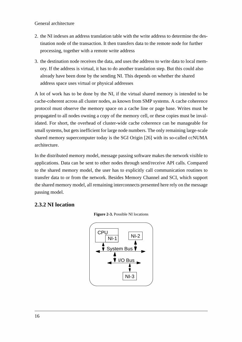
Figure 2-3.Possible NI locations
CPU
NI-3
System Bus
I/O Bus
NI-1 NI-2
16

System Area Networks
bility.
vail-
vel
, it is
nique
ntative
or
inter-
[28]
, the
nta-
search
the
sor
e of
mily
e for
ange
to effi-
egis-
status
ache
on-
high
stem
that
n to a
gh to
vent
The location of the NI inside a system has a great impact on its performance and usa
In general, the nearer it is to the microprocessor, the more bandwidth is typically a
able.
As depicted in Figure 2-3, there are three possible locations for the NI:
NI-1
An interesting solution is support for communication at the instruction set le
inside a microprocessor. By moving data into special communication registers
transferred into the network at a rate equal to the processor speed. This tech
has been realized in the past in some architectures; its most famous represe
is the Transputer [27] from INMOS. Through four on-chip links at full process
clock speed, the Transputer was an ideal candidate as a building block for grid-
connected massive parallel computers. Similar implementations are the iWarp
or related systolic architectures.
Although these architectures are very interesting from the designers view
market for this kind of microprocessors proved to be too small. Most impleme
tions reached the prototype phase, but had no commercial success. Some re
projects also tried to include a network interface at the cache level, but this saw
same fate. Another try in this direction is the Alpha 21364 (EV8) microproces
[29], which has 4 on-chip inter-processor links, each providing a data rat
6.4 Gbyte/s. But Compaq has recently announced the discontinuation of the fa
of Alpha CPUs, so that the EV8 microprocessor will not be fabricated.
NI-2
Assuming a high performance system bus design, this location is an ideal plac
a network interface. Todays system buses offer very high bandwidths in the r
of several Gbytes/s. Common cache coherence mechanisms can be used
ciently observe the NI status. The processor could poll on cache-coherent NI r
ters without consuming bus bandwidth. If the register changes its state (e.g., a
flag is set to indicate message arrival), the NI could invalidate the observed c
line. On the next load instruction, the new value is fetched from the NI. DMA c
trollers can read/write data from/to main memory using burst cycles at a very
bandwidth. Although there are several advantages to design the NI with a sy
bus interface, only a few NIs are implemented in this way. The reason for this is
each processor has its own bus architecture and thus ties an NI implementatio
specific processor. The market for cluster interconnects is not yet large enou
justify such a specialization. Furthermore, commercial interests are likely to pre
17

Design details
n just
d for
s the
d into
PCI
ched
eck
width,
e the
men-
si-
try. A
oher-
host.
mall
nce.
ddi-
mple,
t they
ission
re very
packet
low
r the
2-4
uni-
ut of
ch can
the upcoming of standard processor bus architectures, even though more tha
SANs would benefit from them. Only proprietary interconnects can be designe
the system bus, an example is the SAN adapter of the IBM SP2.
NI-3
Most current interconnects have I/O bus interfaces, mainly PCI. The reason i
great acceptance of PCI as a standard I/O bus. PCI-based NIs can be plugge
any PC or workstation, even forming heterogeneous clusters. A 32 bit/33 MHz
device can deliver a peak data rate of 132 Mbyte/s, which can be nearly rea
with long DMA bursts. To avoid that the PCI bus becomes the main bottlen
between system buses and physical layers with gigabytes per second band
most SANs have already moved on to 64 bit/66 MHz PCI bus interfaces. Sinc
I/O bus even then remains a major bottleneck, SAN developers await the imple
tation of upcoming I/O bus standards like PCI-X [30] and 3GIO [31]. But a tran
tion only makes sense when they are widely used in the mainstream PC indus
disadvantage of the I/O bus location is the loss of properties such as cache c
ence.
Most interconnects presented in this chapter use the I/O bus as their interface to the
2.4 Design details
In the following, a closer look is taken at some specific implementation details. S
modifications of the hardware can have a great impact on the NIs overall performa
This section focuses on various main mechanisms for interconnection networks. A
tional literature [32], [33] is recommended for an even more detailed analysis.
A general rule of thumb could be: Keep the frequent case simple and fast. For exa
mechanisms for error detection and correction should be implemented in a way tha
do not add overhead to error-free transmissions. In the very rare case of a transm
error, some overhead can be accepted, since error rates of current physical layers a
low. The NI should also be able to pipeline data transfers. So the head of a message
can be fed into the network, even if the tail is still fetched from memory. This enables
start-up latencies and good overall throughput.
The term link protocol is used for the layout of messages, which are transmitted ove
physical layer and the interaction between communicating link endpoints. Figure
shows two link endpoints (which could reside in a NI or a switch), connected by two
directional channels for sending and receiving data. Also, it depicts the general layo
a message. Typically, message data is enclosed by special control datawords, whi
18

System Area Networks
ceiver
rate,
bles,
Area
e of
s to
be used to detect start/end of message data and to signal link protocol events (re
cannot accept more data, request for retransmission, etc.).
Figure 2-4.A bidirectional link and the general message format
2.4.1 Physical layer
Choosing the right physical medium of a channel is a trade-off between raw data
availability and cable costs. Copper is still the most used physical medium for link ca
but optical links, which have been broadly used to enhance the capacity of Wide
Networks, are on the verge of penetrating the LAN and SAN markets. Myricom, on
the leading SAN suppliers, announced in July 2001 fiber links and the willingnes
replace all copper-based cables with fiber within a few months.
Figure 2-5.Ultra-fast serial, switched connections replace parallel bus architectures
NI/Switch
Link EndPoint
n bits
Address/Destination
Type/Header
Data/Payload
NI/Switch
Link EndPoint
I/O and system technology
System Area Networks (Myrinet as example)
PCI (parallel bus)PCI-X (133 MHz point-to-point)USB (serial, switched)
SCSI (parallel bus) Hypertransport (serial/parallel, switched)Infiniband (serial/parallel, switched)3GIO (serial/parallel, switched)
ATA (parallel bus)
byte-parallel,copper, 160 MHz
serial, copper,2.5 Gbps
serial, optical fiber,2.5 Gbps
19

Design details
peed
I/O
t and
serial
allel.
idth
SAN
next
tches.
To
ption,
tary
tial
he
en a
built,
les at
ctri-
s can
e more
the
es not
ivi-
urce
ed in
. The
he next
nsfer
Another trend to observe is the replacement of medium-fast parallel links with high-s
serial connections. This is not only true for the SAN market, but also for the whole
infrastructure in PCs and workstations. Figure 2-5 shows this trend by listing curren
future I/O and network technologies. Newest I/O and system technologies start with
implementations, but provide an upgrade path for using multiple connections in par
They all move from a bus-based topology to a full-switched network for better bandw
utilization and easier implementation. Myrinet serves here as an example for the
market. It starts byte-parallel, goes serial, then switches from copper to fiber. The
announced step is the use of multiple serial connections per NIC.
One of the main reasons for using serial connections is the reduced pin count on swi
Latest switch technology with parallel links is limited by the pin count of IC devices.
transmit signals at a high clock rate (200-500 MHz) and a reasonable power consum
the Low Voltage Data Signaling (LVDS) technique (two wires transmit complemen
current levels of signals) is used. So an 8x8 unidirectional switch with 32 bit differen
signal lines would result in 1024 (= (8+8)*32*2) pins only for the links, which is at t
upper limit of todays IC packaging. Bytewide links, as used by most SANs, have be
good compromise for the last years. Network switches of moderate sizes can be
while raw data rate still exceeds the one of serial mediums.
But recent developments have made it possible to transmit signals via copper cab
rates of 1-3 Gbps, with 10 Gbps technology on the horizon. Another limitation of ele
cal transmission at these fast rates is the limited range. Normally, only a few meter
be spanned, until the signals need to be received or refreshed. And signals becom
sensitive to noise effects from parallel bit lines or even other electrical equipment in
surrounding. Optical layers have a clear advantage here, since an optical fiber do
emit any electromagnetic radiation at all. And techniques like Dense Wavelength D
sion Multiplexing (DWDM) or Time Division Multiplexing (TDM) promise to lift the
data rate on optical fibers to 10 Gbps and more.
2.4.2 Switching
The term switching refers to the transfer method of how data is forwarded from the so
to the destination in a network. Two main packet switching techniques, as depict
Figure 2-6, are used in todays networks, store & forward and cut-through switching
first stores a complete message packet in a network stage before the data is sent to t
one. This mechanism needs an upper bound for the packet size (MTU, Maximum Tra
Unit) and some buffer space to store one or several packets temporary.
20

System Area Networks
o the
arded
ique
sion
rred
ge as
finds its
unt
mpli-
arded
rdware
rer to
een
am-
even
wo
-based
In Figure 2-6 (a), packet p0 just arrived at the switch through port 1 and is placed int
packet buffer pool. Packets p1 and p2 have been received in total and are now forw
towards their destination through different ports. This is the common switching techn
found in LAN/WANs, because it is easier to implement and the recovery of transmis
errors involves only the two participating network stages.
Figure 2-6.Packet switching techniques
Newer SANs like ServerNet, Myrinet and QsNet use cut-through switching (also refe
to as wormhole switching), where the data is immediately forwarded to the next sta
soon as the address header is decoded. In Figure 2-6 (b), one sees how a message
way through the network like a ‘worm’. Low latency and the need for only a small amo
of buffer space are the advantages of this technique. But error handling is more co
cated, since more network stages are involved. Corrupted data might be forw
towards the destination before it is recognized as erroneous.
2.4.3 Routing
The address header of a message carries the information needed by routing ha
inside a switch to determine the right outgoing channel, which brings the data nea
its destination. Although a lot of deterministic and adaptive routing algorithms have b
proposed, the latter will not be studied here. Adaptive routing schemes try to find dyn
ically alternative paths through the network in case of overloaded network paths or
broken links. But adaptive routing has not found its way into real hardware yet. T
mechanisms are used in todays interconnects: source-path/wormhole and table
routing [34].
p0
p1
p2
packet pool
port 0
port 1
port 2
port 3
switchswitch switch
switch switch
messagedata flits
(a) (b)
21

Design details
rs a
et. As
chan-
now
source
esti-
ookup
er of
s or
hereas
ths,
the
ch a
fact
aptive
ge is
lock
an reach
e 2-
gress,
g of
In Figure 2-7 (a), an example of wormhole routing [35] is given. A message ente
switch on port 0 and carries the routing information at the head of the message pack
soon as the first dataword is received, routing hardware can determine the outgoing
nel. Used routing data is stripped off, so the routing information for the next switch
leads the message. The entire path to the destination is attached to a message at its
location.
Figure 2-7.Routing mechanisms
In Figure 2-7 (b), a switch containing a complete routing table is shown. For each d
nation node its corresponding port is stored. If messages enter the switch a table l
determines the right outgoing channel. Routing table size is proportional to the numb
nodes, which can be a limiting factor for large cluster configurations with hundred
even thousands of nodes. The former method is easier to implement and faster, w
the latter one provides more flexibility. The routing table could provide alternative pa
if the current addressed path is overloaded. Or based on link utilization information
routing engine could try to find the fastest path towards the destination. But with su
non-deterministic routing one needs to be careful. Link protocols could rely on the
that messages are delivered in order, which is not assured with such a form of ad
routing. Another problem is the prevention of a so-called livelock, where a messa
always routed over alternative paths, but never reaches the final destination.
A problem for both routing mechanisms is the avoidance of deadlocks. A dead
appears when several messages block each other in such a way, that no message c
its destination and the network is blocked in total. This situation is depicted in Figur
8. All messages form a circle of chained, blocked port requests. No message can pro
thus the network is jammed up. One can solve this problem by restricting the routin
switch
port 0 port 1
port 2201
dest-id
id
routing table
port 2
port 2
switch
port 1port 0
(a) (b)
22

System Area Networks
solution
in the
om-
sult
nal the
each
sender
some
redits
not. In
the
into
ender
ome
user-
This
RC on
messages in such a way that these circles of requests cannot appear. One possible
is a strict x-y dimension routing in 2D meshes, where all messages are first routed
horizontal direction, and then vertical. Many other solutions exist [36], more or less c
plex and efficient.
Figure 2-8.Messages forming a deadlock
2.4.4 Flow control
Flow control [37] is used to avoid buffer overruns inside link end points, which can re
in the loss of data. Before the sender can start a transmission, the receiver must sig
ability to accept the data. One possible solution is a credit-based scheme, where
sender gets a number of credits from the receiver. On each packet transmission, the
consumes a credit point and stops when all credits are consumed. After freeing
buffer space, the receiver can restart the transmission through handing additional c
to the sender. Or, the receiver can simply signal the sender if he can accept data or
both cases, the flow control information travels in the opposite direction relative to
data (reverse flow control). For example, Myrinet inserts STOP and GO control bytes
the opposite channel of a full-duplex link to stop or restart data transmission on the s
side.
2.4.5 Error detection and correction
Though todays physical layers have very low error rates, the network must offer s
mechanisms for error detection and possibly correction in hardware. In the era of
level NI protocols, it is no longer acceptable that software has to compute a CRC.
task can easily be done in hardware. For example, the NI adapter can compute a C
switch switch
switch switch
msg0
msg1
msg2msg3
NW
SE
ports
to port E!to port W!
to port N!
to port S!
23
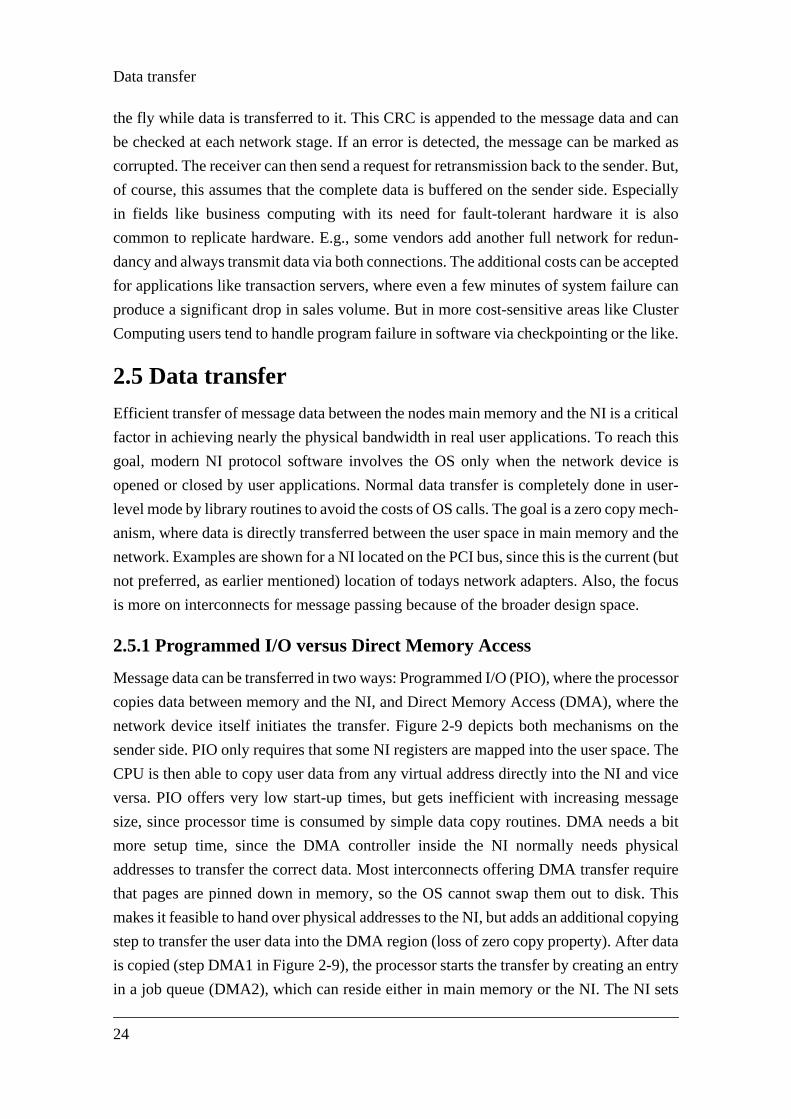
Data transfer
d can
rked as
er. But,
ecially
lso
dun-
cepted
e can
uster
like.
ritical
this
e is
user-
ech-
nd the
t (but
focus
e.
cessor
e the
n the
e. The
vice
sage
a bit
ical
quire
. This
pying
data
entry
ets
the fly while data is transferred to it. This CRC is appended to the message data an
be checked at each network stage. If an error is detected, the message can be ma
corrupted. The receiver can then send a request for retransmission back to the send
of course, this assumes that the complete data is buffered on the sender side. Esp
in fields like business computing with its need for fault-tolerant hardware it is a
common to replicate hardware. E.g., some vendors add another full network for re
dancy and always transmit data via both connections. The additional costs can be ac
for applications like transaction servers, where even a few minutes of system failur
produce a significant drop in sales volume. But in more cost-sensitive areas like Cl
Computing users tend to handle program failure in software via checkpointing or the
2.5 Data transfer
Efficient transfer of message data between the nodes main memory and the NI is a c
factor in achieving nearly the physical bandwidth in real user applications. To reach
goal, modern NI protocol software involves the OS only when the network devic
opened or closed by user applications. Normal data transfer is completely done in
level mode by library routines to avoid the costs of OS calls. The goal is a zero copy m
anism, where data is directly transferred between the user space in main memory a
network. Examples are shown for a NI located on the PCI bus, since this is the curren
not preferred, as earlier mentioned) location of todays network adapters. Also, the
is more on interconnects for message passing because of the broader design spac
2.5.1 Programmed I/O versus Direct Memory Access
Message data can be transferred in two ways: Programmed I/O (PIO), where the pro
copies data between memory and the NI, and Direct Memory Access (DMA), wher
network device itself initiates the transfer. Figure 2-9 depicts both mechanisms o
sender side. PIO only requires that some NI registers are mapped into the user spac
CPU is then able to copy user data from any virtual address directly into the NI and
versa. PIO offers very low start-up times, but gets inefficient with increasing mes
size, since processor time is consumed by simple data copy routines. DMA needs
more setup time, since the DMA controller inside the NI normally needs phys
addresses to transfer the correct data. Most interconnects offering DMA transfer re
that pages are pinned down in memory, so the OS cannot swap them out to disk
makes it feasible to hand over physical addresses to the NI, but adds an additional co
step to transfer the user data into the DMA region (loss of zero copy property). After
is copied (step DMA1 in Figure 2-9), the processor starts the transfer by creating an
in a job queue (DMA2), which can reside either in main memory or the NI. The NI s
24

System Area Networks
into
so it
mple-
in I/O
e an
e done
these
write
l write
odern
rt for
Since
the
ave
(110-
e the
ajor-
n NI
up a DMA transfer to read the message data from memory (DMA3), which is then fed
the network. DMA is not suitable for small messages, but it relieves the processor
can do useful work in case of large messages.
Figure 2-9.PIO vs. DMA data transfer
Several factors influence the performance of both mechanisms. The simplest PIO i
mentation writes message data sequentially into a single NI register, which resides
space. This normally results in single bus cycles and poor bandwidth. To achiev
acceptable bandwidth, the processor must be able to issue burst cycles. This can b
by choosing a small address area as target, which is treated as memory. Writing on
consecutive addresses enables the CPU or the I/O bridge to apply techniques like
combining, where several consecutive write operations are assembled in a specia
buffer and issued as burst transaction. This mechanism can be found in most m
microprocessor architectures. Another solution would be an instruction set suppo
cache control (cache line flush, etc.), as implemented in the PowerPC architecture.
the PCI bus implements variable-length burst transactions, a DMA controller inside
NI could try to read/write a large block of data in one burst cycle. Experiments h
shown that it is possible to reach about 90 % of the peak bandwidth with long bursts
120 Mbyte/s on a 32 bit/33 MHz PCI bus with 132 Mbyte/s peak bandwidth).
To sum it up, PIO is superior to DMA for small messages up to a certain size wher
copy overhead stalls the processor too long from useful work. If one recalls that the m
ity of the typical network traffic is caused by small messages, it becomes clear that a
designer should implement support for both mechanisms.
CPUPIO
System Bus
DMA Space
DataBufferUser
Space
DMA1
DMA2
DMA3
I/OBridge PCI Bus
NetworkRegisters
NI
Main Memory
JobQueue
25
SCI
ech-
sage.
eads
e NI
ent,
poll
rnel
e an
fer. A
int-to-
tech-
orks
s. For
hro-
ased
rcon-
f the
e inte-
ten
ork
.
992)
cting
the
2/64
s, with
2.5.2 Control transfer
If DMA is used for transferring message data, another critical design choice is the m
anism on how to signal the microprocessor the complete reception of a whole mes
This is often referred to as control transfer. In polling mode, the CPU continuously r
an NI status register. The NI sets a flag bit in case of a completed transaction. If th
resides on the I/O bus, this could waste a lot of valuable bandwidth. As an improvem
the NI could mirror its status into main memory. This would enable the processor to
on cache-coherent memory, thus saving bandwidth.
Another solution is to interrupt the CPU. But this results in a context switch to ke
mode, which is an expensive operation. A hybrid solution could enable the NI to issu
interrupt when message data is present for a specific time value without data trans
programmable watchdog timer could be located inside the NI to do this job.
2.5.3 Collective operations
So far, we have only presented mechanisms to send or receive messages in a po
point manner. Software for Parallel Computing often uses collective communication
niques such as barrier synchronization or multicasts. This is especially true with netw
for virtual shared memory, where updated data must be distributed to all other node
example, supercomputers like Cray-X/MP or AlliantFX [38] offered a dedicated sync
nization network. Todays cluster networks leave this task to software, where tree-b
algorithms map a broadcast to a hierarchical send/forward scheme. Only few inte
nects have direct hardware support for collective operations. The barrier register o
Synfinity interconnect [39] is one example.
Networks with a shared bus like Fast Ethernet can easily broadcast data, whereas th
gration into point-to-point networks like Myrinet or ServerNet is more complicated. Of
the hardware realization of collective operations implicates a restriction of the netw
topology. This issue is an area for further improvements of todays cluster networks
2.6 SCI
SCI (Scalable Coherent Interface) [40] is an IEEE standard (ANSI/IEEE Std 1596-1
finally approved in 1992. The goal was to develop a network capable of interconne
multiple systems into one unified distributed memory machine. It should overcome
limitations of bus-based approaches, which have a very limited scalability (up to 3
CPUs). The standard defines a set of hardware protocols and memory transaction
the option of a hardware cache coherence protocol.
26

System Area Networks
mory
ects.
, SCI
over-
speed
scal-
That
of used
emory
s.
M
k
d
s
s
isk
ter-
s
igit
pters
gs,
eir
s
n 3
2.6.1 Targeting DSM systems
Several goals influenced the standardization of SCI as a Distributed Shared Me
(DSM) network. Of course, the premier goal is high performance in all relevant asp
To compete as an interconnect for DSM machines with bus-based SMP systems
needs to provide the same level of data bandwidth, message latency and low CPU
head as its competing architectures. The continuous progress in CPU and memory
should not outrun the network in terms of performance. The second important goal is
ability in many ways. SCI should be able to scale well beyond hundreds of nodes.
relates to the cache coherence mechanism, to the interconnect technology in terms
media and its length, as well as to the addressing scheme to share a terascale m
space.
In the following, the main concepts behind SCI are presented:
• all SCI networks should be build out of unidirectional, point-to-point links. Most
implementations use bit-parallel, copper-based links with a range of a few meter
This is normally sufficient to interconnect a few machines into a tightly-coupled DS
system.
• links should rely on latest signaling technology to provide best performance. Lin
speeds vary today between 500/667 Mbyte/s for SAN cables (LVDS, CMOS) an
1 Gbyte/s for intra-system connections in more advanced, but costly technologie
(GaAs, BiCMOS).
• though it is most common today to interconnect PCs or workstations with SCI, it
intention was also to connect different system components (memory modules, d
arrays, etc.) to an SCI network. But this would require a broad adoption of SCI in
face technology. All relevant systems use either SMP or single-CPU machines a
nodes. SCI can support up to 64k nodes, but real systems use normally a two-d
number of nodes.
• the SCI standard does not specify a specific network topology, but since most ada
have two unidirectional links (1 in-, 1 out-link), common topologies are single rin
or for a larger number of nodes 2D tori or rings of rings. With faster nodes and th
improved single-node bandwidth (PCI 64 bit/66 MHz), the ring structures have
become a significant bottleneck, especially for larger installations. Manufacturer
have responded with small-scale switches (8/16 ports) or adapters with 2, or eve
link connectors to form 2D/3D rings.
27

SCI
e data.
s use
b-
entifier.
it is
nal
ers
PCI,
bility
ation
others.
few
ex
CI
• the transaction layer uses split transactions (request/response) to access remot
The standard defines a limit of 64 outstanding requests, but most implementation
a lower number due to buffer restrictions. SCI provides a global, physically distri
uted 64 bit address space. The upper 16 bits of an address are used as node id
• though coherency is one of the two defining features of SCI (besides scalability),
only included as option in the standard. Due to its complexity and need for additio
resources (cache coherence engine, distributed directory) only few DSM produc
have implemented it. Since most SCI adapters connect to I/O bus technology like
cache coherence is not supported.
2.6.2 The Dolphin SCI adapter
Figure 2-10.Architecture of Dolphin’s SCI card [40]
The SCI standard was intended to specify an open interface to provide interopera
across multiple vendors, connectors and devices. But the complexity of the specific
has led to implementations, which concentrated on necessary features and left out
This resulted in a market with a few proprietary incompatible solutions. Despite a
vendors of DSM systems, like Data General’s AViiON [41] (now part of EMC), Conv
Exemplar [42] (now HP) and Sequent’s NUMA-Q [43] (now IBM), the most used S
SAN implementation is developed by Dolphin Interconnect LCC1.
1. www.dolphinics.com
PCI-SCI-Bridge (PSB)
Link Controller (LC)
TX Buffer RX Buffer
Bypass FIFOSCI InSCI Out
18
PCI Bus
B-Link
PCI Master/Slave
ReadBuffer
WriteBufferProtocol
EngineATC
28
System Area Networks
CI-
B-
ink,
s for a
a
y SCI
be
lso
ated
nced
ets
most
PU-
ram-
nt to
ghput.
into
ke the
write
I link
ered
nt in a
been
e. A
per-
Figure 2-10 depicts the block diagram of the two main chips on the NIC, the PCI-S
Bridge (PSB) and the Link Controller (LC). Both chips communicate via a proprietary
Link bus. This decoupled architecture allows attaching multiple LC chips to the B-L
a separate development of future generations of both chips, and the use of LC chip
non-PCI environment. The main blocks on these chips are:
• the PCI Master/Slave Interface handles all PCI bus transactions. It also contains
DMA controller for direct memory-to-memory transfers.
• Read/Write Buffers contain slots for 128 byte data packets associated with ever
transaction.
• the Protocol Engine manages all SCI transfers. Up to 16 read/write streams can
handles simultaneously.
• the Address Translation Cache (ATC) is used to map PCI to SCI addresses. It a
contains some page attributes. The whole Address Translation Table (ATT) is loc
in separate SRAM on the adapter, an ATC miss triggers are reload of the refere
entry into the ATC.
• TX/RX Buffers on the LC inject/extract SCI packets into/out of the SCI link. Pack
addressing other nodes are simply forwarded via a Bypass FIFO.
The latest version of the PSB (PSB66) offers a 64 bit/66 MHz PCI interface, and the
recent LC (LC3) chip offers a link bandwidth of 667 Mbyte/s. Besides the normal C
initiated read/write transactions some additional features were implemented. A prog
mable DMA engine processes a linked list of control blocks specifying data to be se
remote nodes. This frees the CPU in case of large message transfers for better throu
A feature called mailbox triggers on specially tagged SCI packets, which are placed
a separate message pool. An interrupt is raised on reception of such packets to ma
CPU aware of the received data. Since in a multi-CPU node several concurrent
accesses can occur, a special write gathering is performed to forward data via the SC
in larger data blocks. A store barrier mechanism offers the possibility to flush gath
write data for separate pages.
2.6.3 Remarks
SCI has been used successfully as interconnect in DSM systems, but is less efficie
cluster environment due to certain architectural properties. A lot of components have
optimized for fine-grain communication patterns to support system-wide coherenc
relative small packet size, unidirectional links for ring structures, slow remote read o
29

ServerNet
rcon-
more
gy
rborn
o
band-
lex,
ech-
rarely
s, but
anu-
s. But
siness
d out.
of a
ld by
dem
ich
erv-
ressed
ainly
idth to
erver-
vices,
po-
ters to
ility to
ations, etc. hinder the hardware to unfold its full potential when used as cluster inte
nect. Studies [44] have shown that the sustained node-to-node bandwidth on SCI is
limited than in other networks.
Another bottleneck is the limited ability to form scalable networks. A popular topolo
for SCI is a 2D ring structure, e.g. the largest SCI Cluster in Europe at the Pade
Center for Parallel Computing (PC2) uses an unidirectional 8x12 2D torus. But this als
means that on a ring containing 12 nodes, all these 12 nodes have to share the link
width of 500 Mbyte/s. This is a drawback of SCI systems compared to other full-dup
fully switched solutions like Myrinet or QsNet.
All this led to a relatively low acceptance of SCI as cluster interconnect. While other t
nologies are used now to build Clusters of thousand or more nodes, SCI Clusters are
larger than 32 nodes. Vendors have responded with small-scale (6-8 ports) switche
they can only soften the bandwidth bottleneck. Compared to the SAN market, the m
facturers of SCI-based DSM systems have developed some efficient and fast system
all three mentioned before (Data General, Convex and Sequent) have gone out of bu
or have been taken over by other companies. Most product lines have been phase
2.7 ServerNet
In 1995, Tandem introduced one of the first commercially available implementation
SAN called ServerNet. Since its introduction, ServerNet equipment has been so
Tandem (now owned by Compaq) for more than one billion dollars. In 1998, Tan
announced the availability of ServerNet II [45], the follow-up to the first version, wh
raises the bandwidth and adds new features while preserving full compatibility with S
erNet I.
With ServerNet, Tandem, a major computer manufacturer in the business area, add
one of the main server problems: limited I/O bandwidth. Tandem’s customers, m
business companies running large database applications, needed more I/O bandw
keep up with the growing data volumes their servers should be able to handle. So S
Net was intended as a high bandwidth interconnect between processors and I/O de
but turned quickly into a general purpose SAN.
2.7.1 Scalability and reliability
With scalable I/O bandwidth as the primary goal, ServerNet consists of two main com
nents: endnodes with interfaces to the system bus or various I/O interfaces and rou
connect all endnodes to one clustered system. One main design goal was the ab
30

System Area Networks
data
oves
2-11
Hima-
o the
ses
er-
zers/
sup-
r dis-
rface
po-
xistent
Net I
iodic
con-
transfer data directly between two I/O devices, thus relieving processors of plain
copy jobs. By being able to serve multiple simultaneous I/O transfers, ServerNet rem
the I/O bottleneck and offers the construction of scalable clustered servers. Figure
shows a sample system configuration. Most ServerNet configurations, besides the
laya series of Tandem itself, use an I/O (PCI) adapter instead of directly attaching t
system bus.
Figure 2-11.A sample ServerNet network [46]
2.7.2 Link technology
ServerNet is a full duplex, wormhole switched network. The first implementation u
9 bit parallel physical interfaces with LVDS/ECL signaling, running at 50 MHz. Serv
Net II raises the physical bandwidth to 125 Mbyte/s, driving standard 8b/10b seriali
deserializers to connect to 1000BaseX (Gigabit Ethernet) standard cables. With the
port of serial copper cables, ServerNet is able to span across significantly longe
tances. For compatibility reasons, ServerNet II components also implement the inte
of the first version. Together with additional converter logic, ServerNet I and II com
nents can be mixed within one system, enabling the customer to easily upgrade an e
cluster with components of the new generation without the need to replace Server
components. Links operate asynchronously and avoid buffer overrun through per
insertion of SKIP control symbols, which are dropped by the receiver. Special flow
ServerNetRouter
ServerNetRouter
ServerNetRouter
ServerNetRouter
ServerNetRouter
Discs Discs Discs Discs
ServerNetRouter
ServerNetRouter
ServerNetRouter
ServerNetRouter
ServerNetRouter
ServerServer ServerServer Server Server
31

ServerNet
t have
/write.
yte in
of a
ode
e page
able
the
des-
of sev-
ivery
ge to
odical
ion by
driver
logy.
2. In-
trol symbols are exchanged between two link endnodes to ensure, that data does no
to be dropped due to lack of buffer space.
2.7.3 Data transfer
The basic data transfer mechanism supported is a DMA-based remote memory read
An endnode can be instructed to read/write a data packet of up to 64 byte (512 b
ServerNet II) from/to a remote memory location. The address of a packet consists
20 bit ID and a 32/64 bit address field. The ServerNet ID uniquely identifies an endn
and the route towards the destination.
The address can be viewed as a virtual ServerNet address. The lower 12 bits are th
offset, whereas the upper bits are an index into the Address Validation Translation T
(AVT). Via this indirection, the receiver is able to check read/write permissions of
sender, as depicted in Figure 2-12. To support communication models, for which the
tination of the message is not known in advance, the address can also specify one
eral packet queues, to which data is then appended.
Figure 2-12.ServerNet address space [45]
A main feature of ServerNet is its support for guaranteed and error free in-order del
of data on various levels. On the link layer, a CRC check is done in each network sta
validate the correct reception of the message. Each link is checked through the peri
exchange of heartbeat control symbols. Each endpoint assures correct transmiss
sending acknowledges back to the sender. In case of errors, the hardware invokes
routines for error handling.
2.7.4 Switches
ServerNet I offers 6 port switches, which can be connected in an arbitrary topo
Router II, the next generation of ServerNet switches, raises the number of ports to 1
ServerNet ID
routing table
routing decision
20 bit 20/52 bit 12 bitAVT index offset
address validation& translation table
local physical address
32

System Area Networks
rough
Each
. One
veral
nd-
hich
ver-
sNT
duces
rface
fined
l data
sible
ckets
ms to
erNet
archers
rfor-
put-
hys-
spite
erNet
y is
rnal
and outports contain FIFOs to buffer a certain amount of data and are connected th
a 13x13 crossbar. The additional port is used to inject or extract control packets.
Router offers a JTAG and processor interface for debug or management services
special feature of ServerNet switches is the ability to form so called Fat Pipes. Se
physical links can be used to form one logical link, connecting two identical link e
points. The switches can now be configured to dynamically choose one of the links, w
leads to a better link utilization under heavy load.
2.7.5 Software
The good reliability of the ServerNet hardware makes it possible to implement low o
head protocol layers and driver software. Tandem clusters run the UNIX and Window
operating systems. With its packet queues, the second generation of this SAN intro
a mechanism to efficiently support the message passing model of the Virtual Inte
Architecture (VIA)1 [47], a message layer specification for cluster networks.
To provide an easy way of managing the network, a special sort of packets is de
called In Band Control (IBC) packets. These packets use the same links as norma
packets, but are interpreted by an 8 bit microcontroller. The IBC protocol is respon
for initialization, faulty node isolation and several other management issues. IBC pa
are used to gather status or scatter control data to all ServerNet components.
2.7.6 Remarks
Though it is hard to find detailed performance numbers, ServerNet technology see
be a very reliable and, with its second generation, also high performance SAN. Serv
focuses on the business/server market and has only poorly been accepted by rese
in the area of technical computing so far, though it would be interesting to see the pe
mance of message passing libraries such as MPI and PVM.
ServerNet implements a lot of properties, which are extremely useful for cluster com
ing: error handling on various levels, a kind of protection scheme (AVT), standard p
ical layers (1000BaseX cables) and support for network management (IBC). But de
its commercial success, Compaq has lately announced the discontuinuation of Serv
in favor of the upcoming InfiniBand interconnect. Whether the ServerNet technolog
further developed to fit the Infiniband requirements, or it is abandoned in favor of exte
network technology is not clear yet.
1. www.viarch.org
33

Myrinet
t of
com-
ands
s of
ecifi-
and
om-
The
earch
and
and a
both
sa).
on-
The
net-
MA
y and
2.8 Myrinet
Myrinet [48] is a SAN evolved from supercomputer technology and the main produc
Myricom1, a company founded in 1994. It has become quite popular in the research
munity, resulting in 150 installations of various sizes through June 1997. Today thous
of clusters are equipped with the Myrinet network, with some really large installation
256+ nodes. A major key to its success is the fact that all hardware and software sp
cations are open and public.
The Myrinet technology is based on two earlier research projects, namely Mosaic
Atomic LAN by Caltech and USC research groups. Mosaic was a fine grain superc
puter, which needed a truly scalable interconnection network with lots of bandwidth.
Atomic LAN project was based on Mosaic technology and can be regarded as a res
prototype of Myrinet, implementing the major features such as network mapping
address-to-route translation; however, with some limitations (short distances (1 m)
topology (1D chains) not very suitable for larger systems). Eventually, members of
groups founded Myricom to bring their SAN technology into commercial business.
2.8.1 NIC architecture
Figure 2-13.Architecture of the latest Myrinet-2000 fiber NIC [49]
Regarding the link and packet layer, Myrinet is very similar to ServerNet (or vice ver
They differ considerably in the design of the host interface. A Myrinet host interface c
sists of two major components: the LANai chip and its associated SRAM memory.
LANai is a custom VLSI chip and controls the data transfer between the host and the
work. Its main component is a programmable microcontroller, which controls D
engines responsible for the data transfer directions host to/from onboard memor
1. www.myri.com
2/4/8 Mbyte SRAM
serialfiber linkSAN/fiber
conversion
LANai 9PCIDMA chip
packetinterface
RISChostinterface
PCIbridge
DMAcntl
64 bit data path
SANlink
64/66PCI
34

System Area Networks
fore
, the
gram
om a
cture
ture
n of
PCI-
ter-
z.
NIC
on
-
They
uses
oing
cket
e, the
control
d for
cates
urs
alter-
cked
memory to/from network. So message data must first be written to the NI SRAM, be
it can be injected into the network. This intermediate buffering adds some latency
more the larger the message is. The SRAM also stores the Myrinet Control Pro
(MCP) and several job queues. A recent improvement is the upgrade of the link fr
byte-parallel copper-based implementation to a serial optical fiber. The basic archite
is depicted in Figure 2-13.
More than other SAN developers Myricom has continuously improved the architec
and the hardware components of the Myrinet network:
• the first version of the NIC was based on Sun’s SBus. But with the broad adoptio
PCI and PCs becoming the main node systems instead of RISC workstations, a
based NIC was developed. The first version implemented a 32 bit/33 MHz PCI in
face. A later version upgraded to 64 bit/66 MHz.
• the LANai chip started at 33 MHz, latest versions (v9) are running at 133/200 MH
• on-board SRAM was steadily enlarged, from 512 Kbyte up to latest NIC versions
with 8 Mbyte. This was necessary to satisfy the need for more buffer space on the
to store larger MCPs, provide more space for message data, etc.
• first links were full-duplex byte-parallel links running at 1.28 Gbit/s in each directi
over copper cables up to 10 m. With Myrinet-2000 a serial version of the copper
based links was introduced, running at 2 Gbit/s.
2.8.2 Transport layer and switches
Data packets can be of any length and are forwarded using cut-through switching.
consist of a routing header, a type field, the payload and a trailing CRC. Myrinet
wormhole routing. While entering a switch, the first header byte encodes the outg
port. The switch strips off the leading byte and forwards the remaining part of the pa
to the appropriate output port. When the packet enters its destination host interfac
routing header is completely eaten up and the type field leads the message. Special
symbols (STOP, GO) are used to implement reverse flow control.
On the link level, the trailing CRC is computed in each network stage and substitute
the previous one. A packet with a nonzero CRC entering a host interface then indi
transmission errors. MTBF (Mean Time Between Failure) times of several million ho
are reported for switches and interfaces. On detection of cable faults or node failure,
native routes are computed by the LANai. To prevent deadlocks from long-term blo
35

Myrinet
locking
rts,
ont
e line
ith 8
r a
like
and-
rred
des.
river
ase for
ps to
rity of
ix
tched
messages, time-outs generate a forward reset (FRES) signal, which causes the b
stage to reset itself.
Latest Myrinet switch technology [50] is build around a single crossbar chip with 16 po
called XBar16. A rack-mountable line card equipped with one XBar16 offers 8 fr
panel ports for connecting nodes. 8 ports connect to a backplane interface. Multipl
cards can now be inserted into racks of different size. A backplane is mounted w
XBar16 chips, forming the spine of a Myrinet network. The preferred topology fo
Myrinet network is the Clos network. Compared to other popular network topologies
2D/3D tori/grids, hypercubes, fat trees, etc., a Clos network offers full-bisection b
width, full rearrangability, good scaling and multi-path redundancy. It is the prefe
topology for the latest large-scale Myrinet installations with 256 and more no
Figure 2-14 shows a sample configuration for a 128 node Clos network.
Figure 2-14.A Clos network with 128 nodes [50]
2.8.3 Software and performance
As mentioned before, all Myrinet specifications are open and public. The device d
code and the MCP are distributed as source code to serve as documentation and b
porting new protocol layers onto Myrinet. This has motivated many research grou
implement their own message layers and is one of the main reasons for the popula
Myrinet. Device drivers are available for Linux, Solaris, WindowsNT, DEC Unix, Ir
and VxWorks on Pentium (Pro), Sparc, Alpha, MIPS and PowerPC processors. A pa
GNU C-compiler is available to develop MCP programs.
36

System Area Networks
used
mple-
] and
evel-
quite
The
e Real
m-
r is
earch
rinet
all
ions
seems
ost
ith
flop
The performance of the Myrinet network is highly depended on the software layer
to access the Myrinet hardware. Quite a number of software layers have been i
mented, e.g. Active Messages [51], Fast Messages [52], BIP [53], Parastation [54
many others. Poor quality of early Myrinet software was one issue leading to the d
opment of many external implementations.
Over the last two years, Myricom has developed with the GM message layer [55] a
stable and fast software layer, which is broadly used now for new installations.
second message layer with a significant user base is SCore [56] from the Japanes
World Computing Partnership1 (RWCP). Table 2-3 summarizes basic performance nu
bers for this two layers.
2.8.4 Remarks
The great flexibility of the hardware due to the programmable LANai microcontrolle
one of the major advantages of Myrinet. It has attracted a lot of attention from the res
community and fueled the implementation of lots of message layers on top of the My
network. Another reason for the success is Myricom’s policy of continuous sm
improvements to hardware and software.
Bottlenecks like slow onboard SRAM or LANai chips have been removed, early vers
of low-performance software have been replaced. Regarding market share, Myrinet
to dominate the SAN market right now. With shipping more than 5.000 NICs and alm
10.000 switch ports in 1Q/2001, Myrinet is the network to beat in this area. And w
switch technology scaling to 1.000 nodes and more it is well prepared for future tera
Cluster installations.
1. pdswww.rwcp.or.jp
Table 2-3.Performance of GM and SCore over Myrinet [55], [56]
GMa
a. 66/64 PCI, Myrinet-2000, fiber, LANai 9 200 MHz
SCoreb
b. 33/64 PCI, Myrinet-SAN, copper, LANai 7 66 MHz
sustained bandwidth 245 Mbyte/s 146 Mbyte/s
message size with 50% BWmax 900 Byte 600 Byte
one-way latency 7 us 13.3 us
37

QsNet
drics
s of
only
stem.
le by
chi-
nal
2.9 QsNet
QsNet [57] is a SAN developed by Quadrics Supercomputers World Ltd1. Similar to other
SANs, QsNet has its root in traditional supercomputer technology, since Qua
emerged from the well-known supercomputer manufacturer Meiko Ldt. Influence
their cache-only machines are still visible in the QsNet architecture. QsNet is the
SAN with a seamless integration of the network interface into the nodes memory sy
This unique feature of a globally shared, virtual memory space is made possib
address translation and mapping hardware directly integrated into the NIC.
2.9.1 NIC architecture
Figure 2-15.Block diagram of the Elan-3 ASIC [57]
The third generation of the Elan ASIC is the key component of the QsNet NIC. Its ar
tecture is depicted in Figure 2-15. In the following, a brief description of the functio
units is given:
• a 64 bit/66 MHz PCI interface is used for communication with the host.
1. www.quadrics.com
PCI interface
SDRAMI/F processor
thread mcodeprocessor
DMAbuffers
linkmux
FIFO0
FIFO1
inputter
4 wayset associative
cache
MMU&TLB
tablewalk
engine
clock&statisticsregisters
interconnectionnetwork
into the node
64
64
72
1010
64
28
32
38

System Area Networks
t a
have
rom
o
a
sNet
itch
put
tree
ender
terprets
pecial
ssage
l, all
ent
auto-
net-
are
pace
odel
and to
nchro-
layer,
• full-duplex 10 bit LVDS links connect the NIC via copper cables to the network a
rate of 400 Mbyte/s per direction.
• a 32 bit microcode processor supporting up to four concurrent threads. Threads
different tasks: control of the inputter, setting up the DMA engine, scheduling of
threads, and communicating with the host.
• a 32 bit thread processor, which offloads processing of higher level library tasks f
the host CPU.
• a Memory Management Unit (MMU) with a Translation Look-Aside Buffer (TLB) t
do table walks and translate virtual into physical addresses
• a 64 bit SDRAM interface to connect to external 64 Mbyte SRAM, together with
8 Kbyte on-chip four-way set-associative memory cache.
2.9.2 Switches and topology
Besides the NIC, two different switches (16 and 128 port) are used to connect Q
nodes into a fat-tree network. The basic building block is a line card with 8 Elite-3 sw
chips. Each Elite-3 chip is a 8-port full-duplex switch, with two virtual channels per in
link. Multiple line cards are then used to construct a full-bisection, multi-route fat-
network.
Source-path routing is used to deliver network packets to their destination. The s
attaches a sequence of routing tags to the head of a message. Each network stage in
the first routing tag, removes it and forwards the message towards its destination. S
tags are used to support a broadcast function, which can be utilized to send a me
simultaneously to all remote nodes, or even a group of distinct nodes. At the link leve
network traffic is pipelined in a wormhole manner, with an end-to-end acknowledgm
of packets. In case of transmission errors, the sending NIC retries the transmission
matically without intervention from the host side.
2.9.3 Programming interface and performance
Figure 2-16 shows the overall structure of the programming interface for a QsNet
work. A layer called Elan3lib directly interacts with the hardware. Kernel routines
mainly used for initialization tasks, like mapping parts of a process local address s
into a globally shared virtual address space. The Elan3lib supports a programming m
with cooperating processes. The main functions are used to map/allocate memory
set up remote DMA transfers. Processes communicate mostly via events, e.g. to sy
nize the host process with a thread running on the Elan chip. The Elanlib is a higher
39

QsNet
sage
s both
rtual
syn-
tent
r pro-
ans-
the
nsure
the
the
ort of
rtual
rhead.
pera-
hiding all the hardware- and revision-dependent details. It offers a point-to-point mes
passing model with the use of tags to filter messages at the receiving side. It support
synchronous and asynchronous message delivery.
Figure 2-16.Elan programming libraries [57]
The unique feature of QsNet is its ability to directly send data from a process vi
address space without any intermediate copying. The MMU inside the Elan-3 chip is
chronized to the MMU of the host CPU, or more exact, MMU tables are kept consis
between the QsNet NIC and the OS kernel running on the host node. That way, a use
cess can call a send routine of the Elanlib with a virtual address, the Elan-3 MMU tr
lates the virtual into a physical address, either in main memory or in the SRAM on
QsNet adapter. This is made possible by extending the OS kernel with functions to e
consistency of MMU tables. Special memory allocation functions of the Elanlib offer
possibility to map portions of the on-board SRAM into user processes, e.g. to give
NIC fastest access to DMA descriptor tables.
QsNet currently leads all SANs in performance, due to its advanced hardware supp
message passing primitives. Its unique ability to communicate directly between vi
address spaces without intermediate copies removes a lot of processing ove
Advanced features like a hardware broadcast boost the performance of collective o
Table 2-4.Performance of QsNeta [57]
a. Dual 733 MHz Pentium III, Serverworks HE chipset, Linux 2.4
Elan3lib MPI
sustained bandwidth 335 Mbyte/s 307 Mbyte/s
message size with 50 % BWmax 900 Byte 3 Kbyte
one-way latency 2.4 us 5.0 us
user application
shmem mpi
elanlib
system calls elan kernel routines
user space
kernel space
elan3lib
tport
40

System Area Networks
cale
tures,
ized.
level
imes
ount
er-
their
few
Com-
d pro-
pters,
, this
sified
nter-
AN
ded
f SP
e mid
and
ation
sters.
hines
SP
hite
lops,
tions, like data multicast or synchronization barriers. This is especially true for large-s
clusters with a performance of several teraflops. To make effective use of these fea
the OS kernel has to be patched, and libraries like MPI have to be highly optim
Table 2-4 displays the main performance numbers, both for the Elan3lib and MPI.
2.9.4 Remarks
Though it offers the best performance of todays SANs, QsNet has not attracted the
of attention like e.g. Myrinet. The reason is a relative high price, in the order of three t
the price of competitive solutions. A significant part of the costs is due to the large am
of SRAM on the NIC (64 Mbyte). Quadrics has a strong relationship with the High P
formance Computing division of Compaq. QsNet is the preferred interconnect for
Alpha SC series[58], based on SMP nodes with multiple Alpha CPUs. Though only a
cluster installations exist, these are quite impressive. The latest one is the Terascale
puting System at the Pittsburgh Supercomputing Center (PSC). A cluster of 750 qua
cessor Compaq AlphaServer ES45s, each node equipped with two QsNet ada
delivers a peak performance of 6 teraflops. At the date of installation (October 2001)
system, named ‘Le Mieux’, is the most powerful supercomputer dedicated to unclas
research.
2.10 IBM SP Switch2
Though a proprietary network not intended for the PC cluster market, the Switch2 i
connect [59] from IBM is very similar in its architecture and use to more general S
solutions like Myrinet or QsNet. An intelligent host adapter, driven by an embed
microcontroller, send/receives data to/from the network. The first generation o
Switch technology has been used to interconnect IBM RS/6000 machines since th
90’s. But at the end of the decade it was outdated with its 150 Mbyte/s link bandwidth
slow on-board logic.
To remain one of the top HPC manufacturers, IBM developed with the second gener
of SP Switch technology an interconnect able to keep up the performance of SP clu
Switch2 is a key component for IBM’s RS/6000 SP parallel machines. These mac
are clusters of high-end SMP workstations. Several terascale systems are IBM
machines, among them the most powerful supercomputer today, the ASCI W1
machine. With its 8.192 CPUs in total, the machine is capable of delivering 12.3 teraf
twice as much computing power than the second fastest machine (Le Mieux).
1. www.llnl.gov/asci
41

IBM SP Switch2
tech-
hown
witch
code,
ns are:
e,
s can
the
.
f up
on-
d
Though due to its proprietary interface not usable for general cluster computing, its
nology is quite interesting and therefore, shortly presented here.
2.10.1 NIC architecture
Figure 2-17.Block diagram of the Switch2 node adapter [59]
Figure 2-17 depicts the top-level architecture of the SP Switch2 host adapter. As s
in the figure, one can partition the network adapter into four regions: a high-speed s
interface, a module for data segmentation and reassembly, one for running micro
and one region to interface to the node system. The main components of these regio
• a node bus adapter (NBA) controls the communication with the host via a 16 byt
125 MHz 6XX bus connector. The 6XX bus is the main system bus of the node,
directly connecting the Switch2 adapter to the CPUs and memory modules. CPU
issue load/store instructions to access the adapter.
• a Self Timed Interface (STI) chip connects the adapter via a byte-parallel link to
network. A link is a full-duplex connection driving differential signals at 500 MHz
The link can either be an on-board connection of few inches, or a copper cable o
to 10 meters. The TBIC3 chip is an interface controller, connecting the STI to the
board RAM and the PowerPC 740 microprocessor. It contains hardware to offloa
packet reassembly and segmentation from the main CPU.
PPC
NBA740
SRAM
TBIC3
Bus Connector
STI
MIC
RD
RA
MR
DR
AM
RD
RA
MR
DR
AM
SRAM
microcodeoperations node
interface
high-speedswitch interface
data segmentationand reassembly
500
Mby
te/s
link
42

System Area Networks
AM
IC3.
icro-
ndle
d in
cur at
, the
ng a
th of
host
igher
e host
tors
fter
infor-
data
ing
here
3 sets
fies
hosts
is the
po-
This
twork
er
are
other
• 16 Mbyte of fast Rambus RDRAM is located on the adapter to provide sufficient
buffer space for message data. A Memory Interface Chip (MIC) controls the RDR
and parallelizes multiple accesses to the RDRAM from both the NBA and the TB
• a PowerPC 740 microprocessor is used to control all on-board components via m
code. It is responsible for packet header generation, making routing decisions, ha
error conditions and communicating with the host. Its microcode program is store
4 Mbyte SRAM, along with some other status/control information.
The node architecture is highly decoupled to allow several data transmissions to oc
the same time. While the host CPU is transferring new message data to the RDRAM
PPC 740 may read header information from the RDRAM, and the TBIC3 is forwardi
message from RDRAM to the STI. All those datapaths at least provide a bandwid
1 Gbyte/s, with an aggregate bandwidth of 2.4 Gbyte/s to the RDRAM.
The general purpose PowerPC 740 microprocessor offloads a lot of tasks from the
CPU. It basically provides a low-level message passing interface to the host CPU. H
software layers like MPI or IP then build up on these routines. To send a message, th
simply writes a work ticket into a job queue residing in the SRAM. The PPC 740 moni
this queue, and then sets up the data transfer via DMA from the NBA into RDRAM. A
data is completely written to RDRAM, the microprocessor sets up header and data
mation for the TBIC3, which then forwards data autonomously to the STI. Message
is segmented into 1 Kbyte units. On the receiving side, the TBIC3 forwards incom
header information to the PPC 740 for further investigation. The CPU then decides, w
to place message data and communicates this information to the TBIC3. The TBIC
up DMA transfers to write message data into the RDRAM. Upon completion, it noti
the microprocessor, which then instructs the NBA to write the message out to the
main memory.
Additional to the message transfers, the Switch2 offers some advanced features. On
generation of a Time Of Day (TOD) signal. This signal is used to synchronize all com
nents of the network to a master TOD, even with a compensation of cable delays.
way, a synchronization of the whole network can be maintained at about 1 us.
2.10.2 Network switches
SP machines are mostly connected in a bidirectional multistage interconnection ne
(BMIN) topology. Similar to the fat tree network of QsNet, which is a BMIN, they off
high scalability, multi-route paths and reward communication locality. SP switches
32-port switches, where 16 ports are normally used to connect to nodes, while the
43

IBM SP Switch2
rcon-
heme
with
ata in
t. This
cupies
ing.
ueue.
addi-
m of
is fea-
effi-
the
either
o let
idth
dap-
Three
Ini-
rela-
f the
dapter
f the
ter
e can
level
an-
16 ports are used to interconnect with other switches. Such a switch contains 8 inte
nected 8-port Switch3 [60] chips.
SP switches use source-path wormhole routing with a credit-based flow control sc
to prevent buffer overflow. Each Switch3 chip contains input/output ports, together
a large central buffer queue. This 8 Kbyte central buffer is used to store message d
large chunks in case its targeted output port is blocked by another message in transi
mechanism reduces the head-of-the-line blocking, where a blocked message oc
several network stages and prevents all other messages on this path from advanc
Each output port has two output queues assigned, one low- and one high-priority q
High-priority packets may bypass other messages for faster delivery. Two recent
tions in routing enable better performance for a SP network. First, a restricted for
adaptive routing can be used to let switches determine the fastest network path. Th
ture is especially helpful under heavy workloads to utilize the network in the most
cient manner. Multicast routing is provided via enabling multiple output ports to read
same packet from the central buffer queue. The specification of output ports can be
via a table lookup or encoding of routing bytes.
2.10.3 Remarks
The new generation of IBM’s SP Switch technology offers enough performance t
clusters of RS/6000 SP SMP nodes compete in the HPC market. With a link bandw
of 500 Mbyte/s and a scalable network offering advanced features like multicast or a
tive routing, SP machines are especially well suited for large terascale installations.
out of currently six large teraflop machines of the Accelerated Strategic Computing
tiative (ASCI) are IBM SP systems.
Up to 350 Mbyte/s sustained bandwidth has been measured for MPI applications. A
tive high latency of 17 us could be declared with the highly decoupled architecture o
node adapter. The 6XX bus interface is both an advantage and a drawback. The a
can directly access main memory, without an I/O bridge in between. But the use o
Switch NICs is limited to two versions of IBM’s POWER3 SMP Nodes. For bet
throughput in SMP nodes with up to 8 CPUs, each node board offers two slots, so on
attach two Switch2 adapters to each node.
Features like multicast and adaptive routing have not been implemented with such a
of hardware support in a SAN yet. It will be interesting to see, if and how other SAN m
ufacturers will adopt them.
44
System Area Networks
tems.
d for
her-
among
ared-
ore,
rfor-
com-
and
The
de
de
ased
fini-
, con-
irst
type
at IB
plica-
mand
ter-
rs. It is
et and
ding
and
ith
MA-
urrent
2.11 Infiniband
I/O bandwidth is more and more becoming a limited resource in todays server sys
To overcome this bottleneck, a lot of different I/O technologies have been develope
various application areas. Technologies like PCI, USB, AGP, SCSI, IDE, Firewire, Et
net, Fibre Channel, etc. are used to connect several device classes to a system,
them networking, storage, input/output and graphics. Most of them are outmoded sh
bus architectures, with poor scalability and serious bandwidth limitations. Furtherm
most of them need a significant amount of CPU intervention, eating up a lot of the pe
mance benefit from faster microprocessors and memory modules.
To overcome the architectural limitations of bus-based approaches, several major
puter vendors have worked towards a new standard for I/O connectivity. Future I/O
Next Generation I/O (NGIO) were two competing solutions from different vendors.
need for a unified I/O technology finally led to the formation of the InfiniBand Tra
Association1 (IBTA) in 1999 through a merger of those two forums. Its goal is to provi
a unified platform for server-to-server and I/O connectivity, based on a message-b
fabric network. In October 2000, the organization released the first version of the In
Band specification [61], a three volume set of documents describing the architecture
figuration and use of an InfiniBand fabric.
Companies like IBM [62] and Intel heavily push the development of IB hardware. F
products are available now, but mainly used for software development and proto
demonstrations. With its target to replace different technologies it is expected, th
products first enter the market in one or two main areas and will spread to other ap
tion areas over time. First installations might appear in the storage area, where the de
for bandwidth is extremely high. IB will be first deployed in high-end servers for en
prise-class business applications, like databases, transaction systems or webserve
then expected that the technology moves down into the PC/workstation mass mark
turns into the unified I/O technology it is said to be.
2.11.1 Architecture
Figure 2-18 depicts the general architecture of an IB network. It contains the four buil
blocks: Host Channel Adapter (HCA), Target Channel Adapter (TCA), Switches
Routers. A HCA is an active network interface, similar to a SAN NIC. It interacts w
the host to generate/consume network packets. The HCA provides support for D
based data transfer, memory protection and address translation, and multiple conc
1. www.infinibandta.org
45

Infiniband
erver,
to the
erve
po-
iBand
set
d one
eues,
ledges
d job
ace the
com-
ture
accesses to the network from several processes. A typical HCA location is inside a s
where it interfaces to the system bus via a memory controller to provide fast access
IB network. The TCA is a reduced passive version of the HCA, mainly intended to s
as IB interface for I/O devices like disks, graphics, etc. Switches connect local com
nents into a IB subnet, whereas routers connect the subnet to a larger global Infin
network.
Figure 2-18.The InfiniBand architecture [61]
The foundation of communication in an InfiniBand fabric is the ability to queue up a
of jobs that hardware executes. This is done via Queue Pairs (QP), one for send an
for receive operations. User applications place work requests in appropriate qu
which are then processed by the hardware. On completion, the hardware acknow
the finished job via a completion queue.
Applications can set up multiple QPs, each one independent from the others. A sen
specifies the local data to be sent, and can include the remote address where to pl
data. On the receiving side, a job specifies where to place incoming data. Most of the
munication mechanisms for IB have been adopted from the Virtual Interface Architec
(VIA), a previous standardization effort for communication within clusters.
46

System Area Networks
d ser-
agram
t, net-
tails
ls. It
and
ing
lish-
or
ween
This
two
ts are
n and
InfiniBand supports connection oriented and datagram communication. A connecte
vice establishes a one-to-one relationship between a local and a remote QP. A dat
QP is not tied to a single remote consumer.
2.11.2 Protocol stack
The specification separates IB into several layers, as shown in Figure 2-19: transpor
work, link and physical layer. This layered approach helps to hide implementation de
between layers, which use a fixed service interface to build on each other.
Figure 2-19.InfiniBand layered architecture [61]
Physical layer
The physical layer specifies how single bits are put on the wire to form symbo
defines control symbols used for framing (start/end of packet), data symbols
fillers (idles). A protocol defines correct packet formats, e.g. alignment of fram
symbols or length of packet sections. The physical layer is responsible for estab
ing a physical link when possible, informing the link layer whether the link is up
down, monitoring the status of the link, and passing data and control bytes bet
the link layer and the remote link endpoint.
Link layer
The link layer describes the packet format and protocols for packet operation.
includes flow control and routing of packets within a subnet. It basically defines
types of packets: link management and data packets. Link management packe
exchanged between the two link layers on a connection, and are used to trai
transport
link
physical
layer
layer
networklayer
layer
application
end node
signalingto IB subnet
47

Infiniband
, link
VL)
16
nt)
rt of
spec-
of a
s: an
lds
This
tain
t uses
mul-
ters,
ion.
maintain link operation. They negotiate operational parameters such as bit rate
width, etc. They are also used to convey flow control credits.
Data packets carry a payload of up to 4 Kbyte. A concept called Virtual Lanes (
is used to multiplex a single physical link between several logical links. Up to
different VLs may be implemented, but only VL0 (data) and VL15 (manageme
are required.
Figure 2-20.InfiniBand data packet format [61]
Figure 2-20 depicts the IB data packet format and which layer utilizes which pa
the packet to encapsulate needed information. The Local Route Header (LRH)
ifies source and destination within a subnet, and the VL to use. The payload
packet can be 0-4 Kbyte large. Each packet is completed by two CRC word
Invariant CRC (ICRC) and a Variant CRC (VCRC). The ICRC covers all fie
which should not change during a transmission. The VCRC covers all fields.
combination allows switches and routers to modify header fields and still main
end-to-end data integrity.
Network layer
The network layer implements the protocol to route packets between subnets. I
the Global Route Header (GRH) to identify source and destination ports across
tiple subnets in the format of an IPv6 address. The GRH is interpreted by rou
which may modify the LRH and GRH to forward a packet towards its destinat
48

System Area Networks
struct
a Max-
e
s the
DMA,
ct lost
tion,
ord
oad-
te IB
e an
con-
gies
or
ustry
sible
ader
tions
icant
rface
ient
rcon-
e mar-
Transport layer
The transport layer is responsible to deliver a packet to the proper QP and to in
the QP on how to process the payload. Segmentation of messages larger than
imum Transfer Unit (MTU) is also a task of this layer. It utilizes two fields of th
packet header to accomplish its job. The Base Transport Header (BTH) specifie
destination QP, the packet sequence number and a packet type (send, remote
read, atomic). The sequence number is used by reliable connections to dete
packets. The Extended Transport Header (ETH) gives type-specific informa
like remote addresses, total message length, etc.
An Immediate Data (IData) word of 4 byte can be attached to the packet. This w
is placed on the receiving side into the completion queue entry, allowing to br
cast single data words without transferring payload into DMA areas.
A Software Transport Interface is defined on how to configure, access and opera
communication structures. Additional management services are defined to provid
interface for network-wide configuration and administration of IB components.
2.11.3 Remarks
The aggressive goal of InfiniBand to completely take over the whole I/O and server
nectivity market is a challenging task. It adopts a lot of mechanisms and technolo
from current SANs and tries to apply them to all forms of I/O. Whether it will succeed
fail is also highly dependent on the level of cooperation between the leading ind
companies backing IB. The global approach of InfiniBand stands in contrast to pos
optimizations for a specific application area, as it is cluster computing. E.g., the he
overhead of an IB packet is quite large: up to 106 byte. This means that in applica
with a fine-grain communication pattern the protocol overhead consumes a signif
portion of the physical bandwidth.
On the other hand, competing solutions can try to present an InfiniBand software inte
to applications, while breaking down IB communication structures onto more effic
hardware. At this point, one cannot say if it really becomes the general purpose inte
nect, or ends up as a replacement for SCSI and Fiber Channel in the high-end storag
ket.
49

Infiniband
50

The ATOLL System Area Network
per-
s able
s hand
ple-
ss of
onal
ther.
ilding
. The
rallel
oard,
lso an
net-
des
work.
ay.
Low
of the
e 3-
worm-
cor-
3The ATOLL System AreaNetwork
The idea to develop a new System Area Network was driven by the need for a high
formance cluster interconnect that would reduce costs to a minimum and therefore i
to replace Ethernet as the most commonly used cluster network. Cost reduction goe
in hand with the limited opportunities of a small group of researchers to design and im
ment such a complex network.
So a large scale integration of all components was a major factor guiding the proce
specification and design of a new SAN. This led to the idea to break with the traditi
partitioning of a network into a node interface and switches connecting them toge
The result is a combined interface/switch device, which serves as a single basic bu
block for a new generation of SANs.
3.1 A new SAN architecture: ATOLL
The main idea behind this approach was formulated earlier within another context
first version of ATOLL [63] was designed as a system component for a massive pa
architecture called PowerMANNA [64]. The node design consisted of a quad-CPU b
equipped with PowerPC 620 microprocessors. Besides several memory banks, a
ATOLL chip connects to the system bus to provide a low latency, high bandwidth
work connecting all nodes within a system chassis in a 2D grid. The ATOLL chip inclu
four Bus Master Engines (BME) to give each node CPU exclusive access to the net
Special instructions provide the ability to start communication jobs in an atomic w
This, together with the extreme low latency, gave the design its name: ATOmic
Latency (ATOLL).
Most internal structures have been redesigned, due to the different environment
MPP and the SAN version of ATOLL. But the overall 4x4 structure, as shown in Figur
1, remained as the main characteristic. Several techniques have been adopted, like
hole routing and a mechanism for link-level error correction and retransmission of
rupted data.
51

A new SAN architecture: ATOLL
much
SANs
ions
ar-
uad-
rcome
rces
r the
e for
be a
ation
s with
t I/O
and
llel
s are
re at
Figure 3-1.The ATOLL structure
The number of host and link interfaces is a trade-off between the goal to provide as
performance as possible and what is technically feasible. The bottleneck of todays
is still the network, considering that advanced 64 bit/66 MHz PCI bus implementat
offer a bandwidth of up to 528 Mbyte/s. With PCI-X and its 1 Gbyte/s entering the m
ket, one lets a lot of bandwidth unused. And since dual-CPU, and in the near future q
CPU nodes become an attractive option as cluster node architecture, one can ove
the overhead associated with multiplexing a single NI.
The upper limit for the number of host interfaces is given by the amount of resou
needed to implement them, e.g. control logic, data buffers, etc. The upper limit fo
number of link interfaces is given by the amount of pins needed in the IC packag
implementing the parallel differential signal lines. The 4x4 structure turned out to
well balanced system architecture to completely remove the network as communic
bottleneck for the first time in Cluster Computing.
3.1.1 Design details of ATOLL
Some of the major design decisions are a natural consequence of the experience
other solutions. ATOLL is a message passing network interfacing to the dominan
technology PCI, or more specific, to its latest upgrade PCI-X. It utilizes source path
wormhole routing on the link level to enable very fast data forwarding. Byte-para
copper links were the best choice for the interconnect at the start of the project. SAN
moving now towards high speed serial links, but this technology was still prematu
that time.
hostinterface
hostinterface
hostinterface
hostinterface
linkinterface
8x8crossbar
linkinterface
linkinterface
linkinterface
52

The ATOLL System Area Network
s has
ince
ignal
ia.
ct that
nular-
ques.
other
nter-
level.
ting.
instal-
all
urrent
et-
ngle
nent
a
he
sing
ately,
ple-
etail
A unique technique to detect and immediately correct transmission errors on link
been implemented to remove costly error checking and correction in software. S
newest cabling technology provides an almost errorfree environment, even for high s
speeds, this mechanism offers the possibility to treat the network as a reliable med
The mechanisms for data transfer between the host and the NI were driven by the fa
the performance of DMA- or PIO-based approaches is highly dependent on the gra
ity of the communication. Therefore, the decision was made to support both techni
This will make it possible to pick the fastest transfer, based on message size and
impacts of the node system. A novel event notification mechanism avoids costly i
rupts and enables the CPU to poll on cache-coherent memory.
Some advanced features had to be omitted to keep the complexity at a manageable
It would have been interesting to implement features like adaptive and multicast rou
As discussed earlier, they can give a huge performance boost, especially for large
lations with hundreds of nodes. But the first version of ATOLL targets the market of sm
to medium clusters, with the number of nodes somewhere between 8 and 256. The c
design will be sufficient for these dimensions.
In the following, the major features and mechanisms for the ATOLL System Area N
work are summarized:
• best cost-efficient solution by integrating all necessary SAN components into a si
IC
• support for SMP nodes by multiple independent host interfaces
• removing the need for external switch hardware by integration of a switch compo
• high sustained bandwidth of multiple concurrent data streams by implementing
highly decoupled architecture
• PIO- and DMA-based data transfer to/from host
• efficient control transfer via coherent NIC status information in host memory
• error detection and correction on the link level
The rest of this chapter will introduce the architecture of the ATOLL network chip. T
main focus is on the implemented functionality, and how to make use of it via acces
the control/status registers of the device. Each top-level unit will be described separ
its design and its typical use and operation. Regarding the huge complexity of the im
mentation (over 400 unique modules with about 30.000 lines of code), the level of d
53

Top-level architecture
ered
hould
struc-
sed to
cient
ense
ter-
l archi-
s bus
PCI-
er-
chro-
the
had to be restricted. So not every single state machine or block of control logic is cov
in all aspects. But the description of the most important mechanisms and units s
enable the reader to gain an in-depth insight into the ATOLL architecture.
3.2 Top-level architectureFigure 3-2.Top-level ATOLL architecture
ATOLL is a true 64 bit architecture. All addresses used by the device to access data
tures in main memory have 64 bit base addresses. However, the actual pointers u
reference the start/end of individual data units are 32 bit offsets. This provides a suffi
amount of continuous memory space for data areas (4 Gbyte), while limiting the exp
of internal arithmetic units. When a read/write address is forwarded to the PCI-X in
face, the base address is added to the current offset. Figure 3-2 depicts the top-leve
tecture of ATOLL.
In the following, a brief overview of each functional unit is given:
PCI-X interface
the PCI-X interface is used to communicate with the host system. It can act a
master or slave, and provides sufficient support for latest improvements to the
X bus protocol, e.g. split transactions.
Synchronization interface
since the core of ATOLL runs with a higher clock frequency than the PCI-X int
face, all control and data signals crossing this clock domain border must be syn
nized to prevent signal corruption. This is done in a safe manner by
host linkport 0
8x8linkport 1
linkport 2
linkport 3
port 0
Xbar
net
netport 0
netport 1
netport 2
port 3
hostport 1
hostport 2
hostport 3
port
inte
rcon
nect
sync
h in
terf
ace
PC
I-X
inte
rfac
e
9
64 9+1
64
54
The ATOLL System Area Network
I-X
ible
l four
sfer
s for
er. A
ss data
pply
ssing.
to the
O
t into
sa.
ing
er-
ware
uffer
idth
od-
e data
data
synchronization interface. It also converts the application interface of the PC
interface into a highly independent and concurrent interface for all four poss
data transfer directions (read/write, master/slave).
Port interconnect
the port interconnect multiplexes the access to the PCI-X interface between al
host ports. Sufficient buffer space is provided to assemble multiple tran
requests. It also contains the global status and configuration register set
ATOLL.
Host port
a host port contains all logic to enable PIO- and DMA-based message transf
small interchangeable context keeps all addresses and offsets needed to acce
structures for messages residing in main memory. Large SRAM blocks su
enough buffer space to take up message data and store it for further proce
Multiple concurrent data transfers can be active at a time, e.g. sending data in
network from a FIFO in the DMA unit, while reading data from the receive FIF
of the PIO unit.
Network port
the network port converts a stream of tagged 64 bit datawords from the hostpor
a 9 bit-wide data stream conforming with the link packet protocol and vice ver
Crossbar
the crossbar is a full-duplex 8x8 port switch. It interprets routing bytes of incom
messages to decode the outgoing port, which can be any of the 8 ports.
Link port
the link port provides a full-duplex interface to the network. It prevents buffer ov
run by ensuring a reverse flow control scheme. Special retransmission hard
automatically detects corrupted link packets and retransmits them. Enough b
space is included to support cable lengths of up to 20 m.
The whole architecture is optimized to provide the highest level of sustained bandw
and an extreme low latency. All host/network/link port units consist of independent m
ules for both transfer directions. In contrast to some other SAN interfaces, messag
is not temporary stored in large external RAM modules. Rather multiple smaller
55

Top-level architecture
an be
start-
f the
f using
hable,
cess to
luster
byte
ropro-
es can
s. The
ansfer,
hould
FIFOs are spread all along the data paths from the network to the host. These c
viewed as distributed on-chip data RAM.
3.2.1 Address space layout
The whole ATOLL device requests an PCI-X address space of 1 Mbyte at system
up. Only the first 260 Kbyte if this address space are currently used. Different parts o
address space are assigned separate memory pages to provide the possibility o
varying memory page control schemes. E.g., some pages could be defined as cac
but pages containing status registers should not be cached to make sure, each ac
them returns valid and up to date data. Since the intention is to support all possible c
node platforms (x86, Alpha, SPARC, etc.), the decision was made to select 8 K
pages, since the Alpha architecture uses this memory page size, whereas x86 mic
cessors use 4 Kbyte. So parted address regions with different memory page attribut
be implemented on both platforms.
Figure 3-3.Address layout of the ATOLL PCI-X device
Another reason for separate pages is the level of protection for different address area
user needs access to the registers controlling the PIO- and DMA-based message tr
but the access to critical control registers should be protected. E.g. a normal user s
not be able to alter the frequency of the core clock, or reset parts of the chip.
base address
32 Kbytehost port 0
(4 pages)
host port 1(4 pages)
host port 2(4 pages)
host port 3(4 pages)
cntl/stat regs(1 page)
init/debug regs(1 page)
8 Kbyte
32 Kbyte
32 Kbyte
32 Kbyte
8 Kbyte
unused
unused
(15 pages)
(95 pages)
120 Kbyte
760 Kbyte
+08000h
+10000h
+18000h
+20000h
+22000h
+40000h
+42000h
+FFFFFh
1 Mbyteaddress space
56

The ATOLL System Area Network
left
TOLL
ut any
to the
sses
ed in a
ing of
[18] bit
ld be
ayout.
ppro-
re fur-
cated
isters
In all 8 Kbyte pages only the lower 4 Kbyte part is used. The upper 4 Kbyte are
unused. And read/write accesses to any unused addresses inside the whole A
address space return the data value 0, respectively consume the written data witho
further action. This prevents system failure by erroneous, misaligned accesses
device. Figure 3-3 shows the address layout of the ATOLL PCI-X device. All addre
given are relative offsets to the base address in hex format.
The page for the initialization and debug registers at address 40000h was append
late stage of the design cycle. To ease the insertion of the registers and the decod
addresses, it was simply placed at an address with a unique address bit (a set addr
references the init/debug registers). In further versions of the architecture it cou
located just after the control/status registers to implement a more compact address l
The layout of the different pages is discussed in detail later in this chapter, at the a
priate sections. All four host port address regions have exact the same layout, and a
ther illustrated in the section about the host port. The control/status registers are lo
in the port interconnect and are discussed there. Finally, the initialization/debug reg
are located in the synchronization interface and are specified in its section.
57

PCI-X interface
3.3 PCI-X interfaceFigure 3-4.PCI-X interface architecture [65]
58

The ATOLL System Area Network
yn-
bus
ur
ing
ming
ction
r all
device
e, the
ster
lave
ined
tion
cial
face
ic is
ome
nfig-
dis-
ut
The PCI-X bus interface module used in the ATOLL chip is an external IP cell from S
opsys, Inc [65]. Its top-level architecture is depicted in Figure 3-4. It implements a
interface fully compliant to the PCI-X bus specification[66]. The IP cell is split into fo
main blocks:
DW_pcix_ifc
the DW_pcix_ifc module contains the PCI bus interface. It performs multiplex
of outgoing addresses and data onto the PCI-X AD bus, and registers all inco
signals. Parity generation and checking is part of this module, as well as dete
of the PCI-X bus mode (32/64 bit, 33/66/100/133 MHz).
DW_pcix_com
the DW_pcix_com module implements the Completer logic. It is responsible fo
actions necessary when the device acts as a bus slave. Data written onto the
needs to be forwarded to the application. When addressed by a read cycl
address has to be delivered to the application, which then returns the data.
DW_pcix_req
the DW_pcix_req module contains the Requester logic. It controls all bus ma
transactions triggered by the application. It automatically retries transfers, if a s
device (like the PCI bus bridge) disconnects in the middle of a data transfer.
DW_pcix_config
the DW_pcix_config module implements the PCI configuration space, as def
by the PCI bus specification. It serves read/write requests to the configura
space.
The complexity of the PCI-X bus interface is quite high, since it implements all the spe
protocol cases defined in the specification. This complexity is also visible at the inter
on the application side. But since the functionality needed by the ATOLL core log
quite restricted, a lot of features of the PCI-X interface are ignored and disabled. S
examples are:
• the configuration module provides an interface to the application to read/write co
uration registers, and to modify/control its behavior. This interface is completely
abled, all output signals of the DW_pcix_config unit are left unconnected, all inp
signals are set to their inactive value.
59

Synchronization interface
rrent
. But
on of
p
tions
ation,
pace
xi-
e
long
port
gic.
y the
es in
ester
ta to
ique,
Read,
• the completer interface provides additional signals to force a disconnect of the cu
bus transaction, e.g. when the requested data must be fetched from external RAM
since the ATOLL core can deliver all data within a few cycles, this feature is not
needed, the corresponding signals are disabled.
In the following, the main parameters are given, which were defined during generati
an IP cell adapted to the needs of the ATOLL core logic:
• the device can function as PCI-X or PCI device, as defined during system start-u
• the device is capable of acting as 64 bit bus device. It can request 64 bit transac
and react on them. But it can also fall back into a 32 bit-only mode
• the device is capable of running at the highest bus speed defined by the specific
133 MHz. It also supports lower bus frequencies of 100, 66 and 33 MHz
• a single 64 bit Base Address Register (BAR) is defined, requesting an address s
of 1 Mbyte at system start-up. This address space is defined as prefetchable
• the cache line size register is configured to support up to 4 bits, resulting in a ma
mum cache line size of 16 DWORDS
• no power management functions are implemented
• the registers for minimum grant (MIN_GNT) and maximum latency (MAX_LAT) ar
both set to 255, their maximum value. This signals the request of the device for
bus burst transfers
• the maximum memory read byte count is set to its highest possible value to sup
burst transfers of up to 4 Kbyte
• the signal INTA is used by the device to generate interrupts
• split/delayed bus transaction are supported
3.4 Synchronization interface
The synchronization interface connects the PCI-X bus module to the ATOLL core lo
On the PCI-X side, it implements the completer and requester interface defined b
application side of the unit. The completer interface is used for read/write access
slave mode, when the ATOLL device is the target of a bus transaction. The requ
interface is used for reading data from main memory in master mode, or writing da
memory. On the ATOLL side, these combined read/write interfaces are split into un
and mostly independent paths. This results in four dedicated interfaces: Slave-
60

The ATOLL System Area Network
le of
spe-
picts
with the
side
. The
OLL
tes of
erat-
ucer
t data.
Slave-Write, Master-Read and Master-Write. Between those interfaces, in the midd
the synchronization interface, all control and data signals pass a clock boundary via
cial synchronization elements, which are described in detail later on. Figure 3-5 de
this structure, visualizing the main data flow direction.
Figure 3-5.Structure of the synchronization interface
3.4.1 Completer interface
The completer interface needs to separate read and write accesses, and interacts
Slave-Write and Slave-Read data paths. All signals of the interface used on the PCI-X
are shown in Figure 3-6. The general signals are utilized for both transfer directions
PCI-X bus specification defines several types of read/write bus commands, but AT
only distinguishes between read and write operations. Specifying the number of by
a bus transfer is a new feature introduced with PCI-X, so it has no meaning when op
ing in plain PCI mode. Data is then transferred via a two-way handshaking. The prod
simply signals that data is ready, and the consumer signals that it is ready to accep
synch. fifos
Completer Slave-Write
Slave-Read
init/debugregisters
Requester Master-Read
Master-Write
PC
I-X
inte
rfac
e
AT
OLL
cor
e
clock domain border133 MHz 250 MHz
61

Synchronization interface
of the
g data
ess is
thod
ves
dress.
re to
ough
ion of
rget
ferred,
cycle,
er-
ast
sion
cle.
erted
Transfers occur on each clock edge with both signals set. Detailed timing diagrams
completer interface can be looked up in the databook [65] of the IP cell.
Figure 3-6.Completer interface signals
For write transactions, the completer stores the start address and pushes all incomin
into a synchronization FIFO towards the Slave-Write data path. At the end, the addr
also handed over, together with the number of 64 bit words transmitted. This me
limits write bursts to a length of 64 words, the depth of the data FIFO. But it sa
resources compared to a solution, where each single data word is tagged with its ad
In case of a read request, the address is immediately forwarded to the ATOLL co
request the data. After a few cycles, the ATOLL core delivers the data passing it thr
another 64 word-depth FIFO stage. There is one side condition regarding the relat
both clocks, when the device is in PCI-X mode. PCI-X forbids wait cycles on the ta
side, once the target has started to deliver data. So after the first data word is trans
the target must deliver data on each successive clock cycle.
Since the Slave-Read path on the ATOLL side delivers a data word on each second
the ratio of PCI-X to ATOLL clock frequency must be at least 1:2. So if the PCI-X int
face runs at its highest frequency of 133 MHz, the ATOLL clock must be at le
266 MHz. This restriction is a remnant of an earlier version of the design. A future ver
could simply implement the ATOLL side in a way, so it delivers data on each clock cy
In case of running plain PCI mode, the end of the transfer is signaled via a deass
cdp2app_data [63:0]
cdp2app_bytecnt [12:0]
ifc_addr [18:0]ifc_cmd [3:0]
cdp2app_data_rdy
cdp2app_rdy4data
cdp_64bit_xfrcom_devsel
app2cdp_data [63:0]app2cdp_data_rdy
app2cdp_rdy4data
general
write data to device
read data from device
cdp = completer data pathapp = application
ifc = interfacecom = completer
PC
I-X
inte
rfac
e
ATO
LL c
ore
device is selecteddata is 64 bit widestart address
PCI-X bus commandnumber of bytes
write datadata is ready
app can accept data
read data
cdp can accept datadata is ready
62

The ATOLL System Area Network
so the
FO
64 bit
ions.
ngth
IFO
way
hed if
used
ess. In
d sig-
only
Os of
issing
ssible
s the
device select signal. The completer then deasserts the valid signal for the address,
ATOLL side knows it can stop delivering data. All prefetched data still in the data FI
is then discarded by flushing the FIFO.
For both transfer directions the completer interface is also responsible to convert a
data stream to a 32 bit one, if the PCI-X bus is only capable of running 32 bit transact
3.4.2 Slave-Write data path
Figure 3-7.Slave-Write path signals
On the ATOLL side, the Slave-Write path is plain simple. As soon as an address-le
pair is handed over from the completer, this unit forwards each data word from the F
to the ATOLL core, together with its address. Data is transferred again via a two-
handshaking, the signals are shown in Figure 3-7. On every clock edge, data is latc
it is valid and the consumer side can accept the data. This valid/stop scheme is
throughout the whole architecture to transfer data between adjacent units.
3.4.3 Slave-Read data path
Figure 3-8.Slave-Read path signals
The Completer delivers the address, a valid signal and the byte count for a read acc
case of running in plain PCI mode, the PCI bus does not use a byte count, but instea
nals the end of a transfer via deasserting a signal prior to the last cycle. Since the
burst read access to ATOLL could be the reading of message data from the data FIF
the PIO-mode, a prefetching mechanism is used to not let a request fail due to m
data. So in plain PCI mode, the completer sets the byte count to the maximum po
value. The Slave-Read path now starts to fetch data from the ATOLL core as long a
address is signaled as invalid, or the byte count is satisfied.
SlaveWrite_ValidSlaveWrite_Data [63:0]
SlaveWrite_Address [17:0]
SlaveWrite_Stop
addressdatadata is valid
data can be accepted
SlaveRead_InterfaceFullSlaveRead_DataOut [63:0]
SlaveRead_Address [17:0]
SlaveRead_InterfaceShiftIn
addressaddress is validdata fifo is full
requested data
push data into fifo
SlaveRead_AddressValid
63

Synchronization interface
data
O is
rred
only
data
ersion
nal).
al to
of the
ge as
data
s. An
Figure 3-8 depicts the interface signals to the ATOLL core. In case the core delivers
too fast, e.g. when the PCI-X interface runs only at 33/66 MHz, then a full data FIF
signaled to prevent buffer overflow. When running with 100/133 MHz, data is transfe
every second clock cycle. Below that, the interface is slowed down to transfer data
every fourth cycle. This mechanism was introduced to prevent that lots of prefetched
assembles in the data FIFO, which needed to be shifted out one by one in an early v
of the implementation after the transaction ended (the FIFO simply lacked a flush sig
Later on, a custom version of the data FIFO was developed with such a flush sign
render this mechanism unnecessary. It could be simply removed in a later version
implementation. Figure 3-9 visualizes a typical Slave-Read transfer.
Figure 3-9.Typical Slave-Read transfer
3.4.4 Master-Write data path
When acting as bus master, the ATOLL device tries to transfer data in bursts as lar
possible to use the bus as efficiently as possible. When the ATOLL core writes out
into main memory, each data word is transferred together with its destination addres
address
length
data fifo
control
com
plet
er
ATO
LL c
ore
02048h
8h
requesting 8 words fromaddress 02048h ... address
length
data fifo
control
com
plet
er
ATO
LL c
ore
02048h
8h
ATOLL core startsdelivering data ...
D0
D1
D2 D3
address
length
data fifo
control
com
plet
er
ATO
LL c
ore
02080h
1h
the last data wordsare transferred ...
D7
D8
D9 D12
D10
D11D6
address
length
data fifo
control
com
plet
er
ATO
LL c
ore
rest of prefetched datais flushed!
D9
D10
D11
D12
flush!
(a) (b)
(c) (d)
64

The ATOLL System Area Network
rmal
. It
nuous
d word
rface.
n if
y
s)
ient
man-
spe-
path
unit to
to be
out-
only
nals,
additional signal marks the last data word of a burst. Data is handed over via the no
two-way handshake. Figure 3-10 displays all interface signals.
Figure 3-10.Master-Write path signals
The control logic of the Master-Write data path pushes incoming data into a FIFO
stores the first address and only counts incoming words as long as they form a conti
stream of addresses. At the end of a continuous data block, it hands over address an
count to the requester unit, which then passes the data burst on to the PCI-X inte
There are four conditions marking the end of a burst:
• the address of a data word does not match the previous ones. This might happe
multiple data streams from different host ports are mixed
• the ATOLL signals the last data word of a burst
• the data FIFO is full, so the maximum size for a single burst is reached (currentl
64 words)
• or no data has been transferred for a certain amount of time (currently 128 cycle
3.4.5 Master-Read data path
Reading data from main memory requires more complex logic. To implement an effic
utilization of the PCI-X interface, requests to read data are handled in a split-phase
ner. The ATOLL core issues a request to load a certain number of data words from a
cific address. Up to 32 words can be requested with a single job. The Master-Read
tries to combine successive jobs into one large burst. It then instructs the requester
fetch data from the PCI-X bus and forwards the data to the ATOLL core.
Since multiple host ports might request data, each job is assigned one of 8 job IDs
able to associate returned data with the job requesting it. So up to 8 jobs might be
standing, each with up to 32 words. That way, the PCI-X interface is kept busy and
idles, if no requests for data are active at all. Figure 3-11 shows the interface sig
grouped into signals used for job creation or completion.
MasterWrite_Valid
MasterWrite_DataOut [63:0]MasterWrite_AddressOut [63:0]
MasterWrite_Stop
addressdata
data is validlast data of a burst MasterWrite_last_addr
stop transfer
65

Synchronization interface
ueue.
over
.
n the
a fair
sce-
the
ster
per-
also
nsfer.
g the
Figure 3-11.Master-Read path signals
The control logic of the Master-Read path keeps outstanding jobs in an internal q
Incoming data is then tagged with the correct ID and word count before handing it
to the ATOLL core. Job requests are served strictly in order to ensure a fair service
3.4.6 Requester interface
The requester unit needs to multiplex the access to the PCI-X interface betwee
Master-Write and the Master-Read data paths. Requests for work is scheduled in
round-robin fashion between them to prevent starvation of one of the paths. Both job
narios follow the same procedure, which is briefly described below:
• if a request for a job is handed over by one of the two paths, the requester loads
start address and the byte count into the PCI-X interface
• it signals the type of bus command to the interface. These areMemory Read/
Write Block in case of PCI-X, andMemory Read/Write in plain PCI mode
• data is then transferred via the usual two-way handshaking
• after delivering the last data word, the PCI-X interface is released and the reque
looks for new job requests
In contrast to the completer interface, the conversion of 64 bit data into 32 bit data is
formed automatically by the PCI-X interface. An interruption of the bus transaction is
managed by the interface, e.g. when a bus target disconnects in the middle of a tra
All these special cases are served and managed by the interface, greatly simplifyin
requester logic. Figure 3-12 lists all interface signals of the Requester part.
MasterRead_ValidOutMasterRead_LengthOut [4:0]MasterRead_Address [63:0]
MasterRead_StopOut
address
request is valid
stop transferMasterRead_IDCreate [2:0] new job ID
number of words requested
job creation
job completionMasterRead_Data [63:0]
MasterRead_LengthIn [4:0]MasterRead_IDComplete [2:0]
MasterRead_ValidInMasterRead_ShiftOut
read dataword count of jobID of completed jobdata is valid
shift out data from fifo
66

The ATOLL System Area Network
nter-
ovided,
been
ng in
bit
l bits.
ignor-
of the
Figure 3-12.Requester interface signals
3.4.7 Device initialization
A few initialization and debug registers have been placed into the synchronization i
face. The registers reside on a separate page, because some critical functions are pr
which should only be accessible from a privileged user/administrator. They have
moved out of the ATOLL core, since they cannot assume that a stable clock is runni
the core. Also the configuration of the ATOLL core clock is located here. Only four 64
registers are allocated in total, split up into 32 bit low/high parts.
Figure 3-13 gives an overview about each register and the meaning of its individua
Not all bits are used, these are grayed out. In addition, some registers are read only,
ing write accesses to them. The given address offset is relative to the base address
whole ATOLL device.
app2rdp_data [63:0]
app_bytecnt [11:0]
app_adr [63:0]app_cmd [3:0]
app2rdp_data_rdy
app2rdp_rdy4data
rsm_busyapp_adr_ld
rdp2app_data [63:0]rdp2app_data_rdy
rdp2app_rdy4data
general
write data to PCI-X
read data from PCI-X
rsm = requester state machineapp = applicationrdp = requester data path
PC
I-X
inte
rfac
e
ATO
LL c
ore
start addressPCI-X bus command
number of bytes
write datadata is ready
requester can accept data
read data
app can accept data
data is ready
load address, start jobrequester is busy
67

Synchronization interface
Figure 3-13.Device initialization and debug registers
resetreg 0 lowread/write
31 0
hp_res_n[3:0]63 32pllreg 0 high
offset: 40000hread/write
lp_res_n[3:0]np_res_n[3:0]
pi_res_n
xbar_res_nclk_sel_res_n
not_used
feedback cnt[5:0]for XO-PLL
avoid_glitch
slave_select [1:0]
master/slave_select
not_used
n/areg 1 lowread/write
31 0
63 32statusreg 1 high
offset: 40008hread only
not_used
pcix_mode
PCI-DLL lock
not_used
ifc_bus64
pcix_66m
pcix_100m
pcix_133m
bist_start_lowreg 2 lowread/write
31 0
63 32bist_start_highreg 2 high
offset: 40010hread/write
not_used
PCI-DLL bypass
xxx port 0bist_start [9:0]xxx port 1
bist_start [9:0]
xxx port 2bist_start [9:0]
xxx port 3bist_start [9:0]synch. int. (Mst-Wr)
synch. int. (Mst-Rd)
synch. int. (Slv-Wr)
bist_ok_lowreg 3 lowread only
31 0
63 32bist_ok_highreg 3 high
offset: 40018hread only
not_used
xxx port 0bist_ok [9:0]xxx port 1
bist_ok [9:0]
xxx port 2bist_ok [9:0]
xxx port 3bist_ok [9:0]synch. int. (Mst-Wr)
synch. int. (Mst-Rd)
synch. int. (Slv-Wr)
68

The ATOLL System Area Network
een
art of
ost
the
bit
h its
the
er
tran-
ts at
and
ck
ks
erns.
an-
tests
IST
ells
buf0,
. An
Reset register
besides the global power-on reset signal, each major block of ATOLL has b
assigned a unique reset signal. This offers the possibility to reset a specific p
the device without reinitializing the whole chip. The abbreviations stand for: h
port (hp), network port (np), link port (lp ), port interconnect (pi ), crossbar
(xbar ) and clock logic (clk_sel ).
PLL register
the ATOLL clock logic includes a configurable Phase Locked Loop (PLL) to set
internal clock to anywhere within 175-350 MHz, in steps of 14 MHz. The 6
feedback counter configures the clock frequency. Besides running a chip wit
own clock, there is the possibility to take one of the four incoming clocks from
links as main clock signal. Which one is selected viaslave_select [1:0] .
The signalmaster/slave_select is then used to switch between the mast
and the selected slave (link) clock. Another signal can be set to make sure this
sition is made without glitches on the clock signal.
Status register
The lower 5 bits sample some status bits set by the PCI-X interface. It detec
system start-up, if it runs in PCI or PCI-X mode, whether it sits on a 64 bit bus,
which PCI bus frequency is configured. The signalPCI-DLL lock is set, when
the on-chip Digital Locked Loop (DLL) has adjusted the PCI clock to a fixed clo
tree delay, as specified in the PCI-X specification.
BIST start register
All SRAM memory cells have a Built-In Self Test (BIST) logic attached. It chec
the memory for erroneous bits by successive reads/writes of certain bit patt
This is done normally via the JTAG test logic, which is used to check chips for m
ufacturing faults. But these registers provide an additional way to run the BIST
via software. Setting the start bits triggers the internal control engine of the B
logic to run through all memory cells. Each bit controls one of the 43 SRAM c
in the ATOLL chip.
All cells within a 10 bit word of xxx port 0/1/2/3 are in the same order
([0:9]): hp_pio_snd, hp_pio_rcv, hp_dma_snd, hp_dma_rcv, np_snd, np_rcv_
np_rcv_buf1, lp_in, lp_out_buf0, lp_out_buf1.
Three bits are used to control the three SRAMs in the synchronization interface
additional bit is used to bypass the PCI-DLL.
69

Port interconnect
sizes
s are
AM.
BIST ok register
These bits are the corresponding signals to the BIST start bits. Due to different
of the SRAMs some checks are faster than others. But after 10 us all SRAM
tested, and all 43 bits should be set. Any bits remaining unset flag a flawed SR
3.5 Port interconnectFigure 3-14.Structure of the port interconnect
Slave-Write
control/statusregisters
sync
hron
izat
ion
inte
rfac
e
host
por
t 0ho
st p
ort 1
host
por
t 2ho
st p
ort 3
cntl
cntlSlave-Read
port interconnect
cntlMaster-Write
arbiter
cntlMaster-Read
arbiter
70

The ATOLL System Area Network
hro-
ead,
men-
from
enta-
ossi-
ther
from
done
e 56.
FIFO.
vering
ing the
ll host
ports.
gnal is
event
a fair
sters,
The
ions
ory,
4 bit
e of
t port
isters
d by
wing
The port interconnect multiplexes the four ATOLL core data paths described in “Sync
nization interface” on page 60 between all four host ports: Slave-Write, Slave-R
Master-Write and Master-Read. It temporary buffers data in FIFOs to ease the imple
tation as an IC. The data nets would otherwise travel a long distance across the chip
the host ports to the synchronization interface, making the task of a physical implem
tion extremely difficult. And some additional pipeline stages on each path give the p
bility to assemble a few data words in this module, even if the path is blocked fur
ahead.
The implementation of both Slave paths is straight forward. An incoming address
the synchronization interface is decoded to find out the target host port. This can be
by analyzing only 2 bits of the address, according to “Address space layout” on pag
In case of the Slave-Write path, the addressed host port then pops the data from the
If data should be read from one of the host ports, the addressed host port starts deli
data, until the Slave-Read path deasserts the valid signal for the address, thus end
transfer. Both data paths also handle requests for the control/status registers.
In case of both Master paths, the access to them must be multiplexed between a
ports. Each path contains an arbiter, which observes request signals from the host
It grants the data path to only one host port, and releases the grant, if the request si
deasserted. This is forced by a host port itself after a specific amount of cycles to pr
one host port blocking the access to the data path. Arbitration is done based on
round-robin schedule policy. The Master-Write path is multiplexed between 8 reque
since two individual units inside each host port need to write data out to memory.
main unit is the one receiving messages in DMA mode, spooling data out to buffer reg
residing in main memory. The other unit mirrors relevant status information into mem
removing the need to poll the device for it. These status packets consist of only four 6
data words, thus the impact on the overall data throughput is relative small.
3.5.1 ATOLL control and status registers
A separate module1 hosts the control/status registers needed for managing the us
ATOLL. These are registers configuring the global state of the device, as well as hos
specific registers. Since they control important settings of the device, these reg
should not be visible nor accessible to the normal user. They are normally controlle
a supervisor, mostly via an administration interface. These registers provide the follo
functionality:
1. designed and implemented by Prof. Dr. Ulrich Brüning
71

Port interconnect
. The
nt the
l reg-
f side
tus of a
vice
it. The
ey are
t link
cribed
)
• link driver control
• start/stop of DMA engines
• interrupt generation (mask & clearance)
• global counter
• debug control of the crossbar
• additional status information
All registers can be split into four categories: control, status, debug and extension
registers are aligned to cache line boundaries of eight 64 bit words. This is to preve
CPU from fetching more than one register with each access, possibly loading severa
isters into prefetch buffers in the system’s chipset. Though all registers are free o
effects, this decision was made to ensure that a user always gets the up to date sta
register.
In Table 3-1, all control registers are listed with their address offset relative to the de
base address, their mode (read/write, read-only) and whether they use 32 or 64 b
status registers make various status information visible to the user of the device. Th
listed in Table 3-2 in the same manner as in the previous table.
The internal crossbar offers the possibility to observe its status and to insert/pull ou
data in case of severe problems. Table 3-3 lists the eight registers, their use is des
in detail in the ATOLL Hardware Reference Manual [67].
Table 3-1.Control registers of ATOLL
register name offset mode, width comment
hw_cntl 20000h r/w, 32 hardware control, link enable, DMA engines
cnt_load 20040h r/w, 64 global counter load
hp_cntl 20080h r/w, 64 host port specific control
hp_dma_thres 200C0h r/w, 32 threshold value to determine receive mode (DMA/PIO
irq_timeout 20100h r/w, 32 IRQ time-out value
irq_mask 20140h r/w, 32 IRQ mask setting
irq_clear 20180h r/w, 32 IRQ clearance
hp_timeout 201C0h r/w, 32 host port time-out value for PIO mode
72

The ATOLL System Area Network
ontrol
e chip,
nc-
Finally, two more registers are used as extension to the above set of registers to c
the debugging of the crossbar and to read/write data on 8 general purpose pins of th
as listed in Table 3-4.
In the following, all registers are described in detail. They are listed in groups of fu
tional classes, rather than in the strict sequence given in the tables.
Table 3-2.Status registers of ATOLL
register name offset mode, width comment
hw_state 20200h ro, 32 hardware state, clock configuration, DMA engines
cnt 20240h ro, 64 global counter value
hp_state 20280h ro, 32 host port specific status, last mode of access
lp_retry 202C0h ro, 32 link port retry counter
hp_irq_case 20340h ro, 32 host port IRQ cases, out of buffer space
irq_case 20380h ro, 32 global IRQ cases, link error, clock failure
Table 3-3.Debug registers of ATOLL
register name offset mode, width comment
debug_xbar0 20400h r/w, 64 debug info from crossbar port 0
debug_xbar1 20440h r/w, 64 debug info from crossbar port 1
debug_xbar2 20480h r/w, 64 debug info from crossbar port 2
debug_xbar3 204C0h r/w, 64 debug info from crossbar port 3
debug_xbar4 20500h r/w, 64 debug info from crossbar port 4
debug_xbar5 20540h r/w, 64 debug info from crossbar port 5
debug_xbar6 20580h r/w, 64 debug info from crossbar port 6
debug_xbar7 205C0h r/w, 64 debug info from crossbar port 7
Table 3-4.Extension registers of ATOLL
register name offset mode, width comment
debug_cntl 20600h r/w, 32 control of crossbar debug
gp_io 20640h r/w, 32 8 general purpose I/O pins
73

Port interconnect
r reg-
LL
r.
e now
its
the
Figure 3-15.Hardware control/status and global counter
Figure 3-15 depicts the hardware control/status register, as well as the global counte
isters. The latter is simply an internal counter, which is running with the internal ATO
core clock. A write access to thecnt_load register loads the written value into the counte
The hardware control/status registers assemble various configuration bits, which ar
described in more detail:
• hw_cntl[7:0] enables the DMA engines inside the four host ports. The lower four b
control the DMA engines in the receive unit, whereas the upper four bits control
send DMA units. These bits are helpful, if the context of the host ports should be
switched, e.g. in case the device is multiplexed between several user processes
hw_cntlreg 0read/write
31 0
offset: 20000h
hp[x] enable
not_used63
DMA rcvhp[x] enableDMA snd
[x] = [3:0]
lp[x]loopback
link retrymux [1:0]
link[x]driverenable
xbar debugmode enable
hw_statereg 8read-only
31 0
offset: 20200h
hp[x] DMA
not_used63
snd idlehp[x] DMArcv idle
[x] = [3:0]
link[x]activelink[x]
PLL lockXO PLL lock
internal PLL lock
clk phase synch.
cnt_loadreg 1read/write
31 0
offset: 20040h
63
load written valueinto 64 bit global counter
cntreg 9read-only
31 0
offset: 20240h
63
64 bit global counter,running with internal core clock
74

The ATOLL System Area Network
lly
rt.
t
the
re it
ns
r
the
.
the
s:
the
et-
ir-
bit
et to
or up
ord
ed, if
e
ord
• hw_cntl[15:12] controls a loopback mode of the link ports. Message data norma
sent over the link is then fed back into the device via the input path of the link po
This is helpful to isolate cable failure from internal chip problems
• hw_cntl[17:16] controls the generation of an interrupt based on link bit errors. Bi
errors force a link packet retransmission by the link port. This event is signaled by
link port, and accumulated in internal 4 bit counters.link_retry mux[1:0] determines
the significant bit of the accumulator, that triggers an interrupt. So one can configu
in a way that an interrupt is generated after 1, 2, 4 or 8 link packet retransmissio
• hw_cntl[23:20] enables the LVDS driver I/O cells, so link data is driven over the
cable
• hw_cntl[31] is used to activate a special mode for the crossbar debug registers
• hw_state[7:0] signals idling DMA engines in the host ports. This is useful to wait fo
completion of DMA jobs, after the DMA engines have been disabled. By accident,
bits for send/receive have been switched in relation to thehw_cntl bits
• hw_state[23:20] are set, if the corresponding link is active
• hw_state[27:24] are set, if the corresponding link PLL is locked
• hw_state[30:28] are set, if the two PLLs for the main ATOLL core clock are locked
The highest bit is set, if the phases of two clock signals are synchronizes, when
main clock should be switched from the on-chip clock signal to a link clock
Figure 3-16 shows the registers to control the host ports. Their meaning is as follow
• hp_cntl[3:0] determines the update frequency of status information written out by
PIO receive unit inside a host port. After n words have been received from the n
work and pushed into the 64 word data FIFO, the unit triggers an update of the m
rored FIFO fill level in main memory. To span the whole range of the FIFO, the 4
value is multiplied by 4, so updates can occur after 4, 8, 12, 16, ..., 60 words. If s
0, this mechanism is disabled. Setting this value is a trade-off between the need f
to date status information and limiting the bandwidth used for updates. The last w
of a message frame (header or data) always triggers the update, so one is inform
enough or all remaining data is available
• hp_cntl[7:4] does the same job, but for the PIO send module. If the fill level of th
FIFO varies by the threshold value, an update is triggered. Also writing the last w
of the data frame triggers an update
75

Port interconnect
it
rtion
(nor-
pro-
of an
th of
• hp_cntl[31:8] have the same meaning likehp_cntl[7:0], but for the other host ports
Figure 3-16.Host port specific control/status registers
• hp_cntl[56, 48, 40, 32] can be used to disable the immediate forwarding of data
written into the PIO send data FIFO towards the network. If set, the PIO send un
waits, until all data of the message is written to the FIFO. This prevents the inse
of incomplete messages into the network in case the user process is interrupted
mal process scheduling, interrupt service) or simply crashes due to an error in the
gram code
• the 8 bit values specified in thehp_dma_thres register are used to determine the
mode used to receive a message. This threshold value is compared to the length
incoming message in the receive part of a host port, or more specific, to the leng
hp_cntlreg 2 lowread/write
31 0
63 32hp_cntlreg 2 high
offset: 20080hread/write
hp[0] rcv
hp[0] PIO
not_used
hp_dma_thresreg 3read/write
31 0
offset: 200C0h
not_used63
hp[0] DMA
updatehp[0] sndupdate
hp[1] rcvupdatehp[1] snd
update
hp[2] rcvupdatehp[2] snd
update
hp[3] rcvupdatehp[3] snd
update
snd completehp[1] PIOsnd complete
hp[2] PIOsnd complete
hp[3] PIOsnd complete
thresholdhp[1] DMAthreshold
hp[2] DMAthresholdhp[3] DMA
threshold
hp_timeoutreg 7read/write
31 0
offset: 201C0h
not_used63
hp[0] PIOtimeouthp[1] PIO
timeout
hp[2] PIOtimeouthp[3] PIO
timeout
hp_statereg 10read-only
31 0
offset: 20280h
not_used63
hp[0] PIOrcv tags
hp[0] PIOsnd lastmode
hp[1] PIOrcv tags
hp[1] PIOsnd lastmode
hp[2] PIOrcv tags
hp[2] PIOsnd lastmode
hp[3] PIOrcv tags
hp[3] PIOsnd lastmode
76

The ATOLL System Area Network
ceive
are
PIO
d
all
ork.
it of
17.
,
nted.
t of
In
ble to
oft-
cess.
to the
g the
gs of
mes-
three
f a
the data frame. It is forwarded to the DMA-receive unit, if the length is greater or
equal to the threshold value. So setting it to 0 pipes all messages to the DMA-re
unit, disabling the PIO mode for receiving messages. Since length and threshold
specified in terms of 64 bit data words, the largest message to be received via the
mode is 254*8=2032 byte large, if the threshold is set to FFh
Figure 3-17.Loading the PIO-receive time-out counter
• thehp_timeout register specifies an upper limit for the time data has been pushe
into the data FIFO in the PIO-receive unit without reading it. This mechanism sh
prevent data to clog in the host port and to block a path backwards into the netw
An internal 32 bit counter is loaded with the 8 bit time-out value each time a data
word is shifted in or out of the FIFO. To span a large time segment, each second b
the upper 16 bit is loaded with a bit from the time-out value, as shown in Figure 3-
This makes it possible to configure a time-out of up to 5.7 s, with steps of 262 us
assuming a 4 ns clock cycle. Each cycle nothing happens, the counter is decreme
If it runs down to 0, an interrupt is generated to force the host to pull the data ou
the host port
• thehp_state register provides some information about the status of the PIO unit.
case of an interrupted or incomplete PIO-based message transfer, one must be a
recover the situation, avoiding the need to reset the complete device. So driver s
ware needs to be able to detect, in which state the PIO unit was left by a user pro
In case of the PIO-Send module, this register shows the mode of the last access
unit. More specific, it shows the tags of the last data word written to the FIFO.
According to the tags, driver software is able to complete the message by writin
missing data to the FIFO. In case of the PIO-Receive unit, one simply sees the ta
the data word at the head of the FIFO. So software is able to pull out the rest of a
sage one by one. The 4 bit tags are {Last, Data, Header, Route}, according to the
frames a message is composed of, and an additional bit to mark the last word o
frame
timeout value07
31 16
32 bit timeout counter
123456
0
1
0...00
1 1 1 0 0 0 0
1 1 1 1 0 0 0 000000000
77

Port interconnect
upts.
condi-
ail in
le to
e rest
the
Figure 3-18.Interrupt registers
Figure 3-18 gives an overview about all registers related to the generation of interr
There are various sources for interrupt generation, and a user is able to mask those
tions, which should not result in a system interrupt. Each register is described in det
the following:
• the irq_timeout register is used in case the host system has crashed and is not ab
serve an interrupt. In such a case, the node should not block communication in th
of the cluster by letting pending incoming messages block paths backwards into
irq_timeoutreg 4read/write
31 0
offset: 20100h
not_used63
32 bit IRQ timeout value
irq_maskreg 5read/write
31 0
offset: 20140h
not_used63
mask bits corresponding to irq_case
irq_clearreg 6read/write
31 0
offset: 20180h
not_used63
clear corresponding IRQ bit in irq_case
hp_irq_casereg 13read-only
31 0
offset: 20340h
not_used63
hp[0] irq casehp[1] irq case
hp[2] irq casehp[3] irq case
hp[x] irq case[4:0] = unused hp[x] irq case[6] = data region fullhp[x] irq case[7] = desc. table fullhp[x] irq case[5] = access to empty fifo
irq_casereg 14read-only
31 0
offset: 20380h
not_used63
lp[x]
xbar-in
xbar-outretryhp[x]
PIO rcverror
hp[x]DMA rcverror
link[x]cableplugged
link[x]cableremoved
link[x]clockactive
link[x]clockfailure
78

The ATOLL System Area Network
e all
e, an
y
is
ond
0
er-
ive
e
e the
he
s, but
ths
nk.
hey
re
ey
network. In case of such a severe system failure, the device should simply consum
incoming data traffic. So every time an interrupt request is signaled by the devic
internal counter is loaded with this time-out value. If it runs down to 0 without an
reaction from the host side, it is assumed that the host is down. This information
then flagged to all units
• the irq_mask register is used to mask specific interrupt sources. The bits corresp
to the IRQ bits in theirq_case register. An interrupt is masked, when its bit is set to
• the irq_clear register is utilized to clear a corresponding interrupt in theirq_case
register. Writing a 1 to a bit clears the interrupt
• thehp_irq_case register offers some more information in case an interrupt is gen
ated by a host port. It flags a read access to an empty data FIFO in the PIO-rece
unit. In case of the DMA-receive module, two data buffers in main memory can b
filled to a level, where no more messages can be written out to memory. These ar
descriptor table and the data region. These events are flagged by this register. T
remaining 5 bits of a byte used for each host port were used in previous version
late modifications rendered them unnecessary
All possible interrupts are flagged by theirq_case register. The specific bits are
described in the following:
• irq_case[3:2] are set if error conditions occur in one of the input or the output pa
of the crossbar
• irq_case[7:4] flag an amount of bit errors and link packet retransmissions on a li
The actual limit for the generation of this interrupt is controlled via the two
lp_retry_mux bits in thehw_cntl register
• irq_case[11:8] are used to flag an error in the PIO-receive units of a host port. T
were intended to be the ‘logical OR’ of all possible PIO error conditions, which a
then specified in thehp_irq_case in detail. But due to late modifications all but one
error condition were dropped, so these bits are basically the same as thehp[x] irq
case[5] bits, showing a read access to an empty PIO-receive data FIFO
• irq_case[15:12] show a general error in the DMA-receive units of a host port. Th
are the ‘logic OR’ of the two error conditions specified in thehp_irq_case register
• irq_case[23:20] andirq_case[19:16] observe the status of link active signals and
are set, if a link cable is plugged or unplugged
79

Port interconnect
ks
e of
cket
ange.
nt ones,
of the
ard-
le to
ter-
us
r-
g
• irq_case[31:28] andirq_case[27:24] observe the status of the associated link cloc
and flag their activity or failure
Figure 3-19.Link retry register
The lp_retry status register, as shown in Figure 3-19, provides for each link the valu
an 8 bit accumulator counting bit errors on links and the corresponding link pa
retransmissions. They can be used to measure bit error rates over a greater time r
Besides the registers presented over the last pages, there are other, less importa
which are not described in detail here. There is an additional registergp_io to control
8 general purpose I/O pins. And some registers are used to debug the internal status
crossbar. More specific information about them can be looked up in the ATOLL H
ware Reference Manual [67].
In the following, a typical interrupt service sequence is given:
• assuming the descriptor table of host port 3 is full and the receiving part is not ab
spool out a new message to memory, the host port would flag this event to the in
rupt control unit
• this unit compares the event with the corresponding bit in theirq_mask register to
make sure the event is not masked
• it then raises the interrupt line, which is driven out to the PCI-X bus by the PCI-X b
interface
• a system trap calls the ATOLL driver software to deal with the interrupt
• the driver software checks theirq_case register to figure out the reason for the inte
rupt
• it allocates memory space for the descriptor table, either by enlarging it or movin
messages in a temporary buffer
lp_retryreg 11read-only
31 0
offset: 202C0h
not_used63
lp[0] retrycounterlp[1] retry
counter
lp[2] retrycounterlp[3] retry
counter
80

The ATOLL System Area Network
the
are
r
mall
esiding
rated,
ork.
le data
• the interrupt is then cleared by the software by writing to the corresponding bit of
irq_clear register. The host port resumes processing messages as soon as there
again free slots in the descriptor table
3.6 Host portFigure 3-20.Structure of the host port
The host port [68]1 is the main building block of the ATOLL chip. It is responsible fo
data transfer from or to the network, either by PIO or DMA. Each host port has a s
working set of some status and control registers needed to access data structures r
in main memory. Data paths for sending and receiving messages are strictly sepa
offering the possibility of multiple concurrent data transfers into and out of the netw
Each mode is also handled separately, so four unique modules are used to hand
1. Berthold Lehmann implemented an early simulation model of the host port
PIO-send
replicator
netw
ork
port
cntl
port
inte
rcon
nect
DMA-sendcntl
64x68 data fifo
event buffer
64x68 data fifo
64x68 data fifo
PIO-receivecntl
64x68 data fifo
cntlDMA-receive
status/controlregister file
hp2nppath
np2hppath
81
Host port
the
or is
ves a
ll the
acing
en the
o the
f the
t inter-
repli-
-send
n the
ords
pen-
picts
of an
TOLL
trans-
based
3-22
eparate
uses
ferent
ide
transfer: PIO-send, PIO-receive, DMA-send and DMA-receive. Another unit keeps
working set and interfaces with all transfer modules. A sixth module called replicat
responsible to update relevant status information residing in main memory. This gi
CPU fast and cachable access to information without the need to frequently po
device. Finally, two units are used to control the access of the host port to the interf
network port. In case of sending messages, the access must be multiplexed betwe
PIO- and DMA-send units. For incoming messages, one must forward them either t
PIO- or the DMA-receive unit. This decision is configurable and relies on the size o
incoming message. Figure 3-20 depicts the overall structure of a host port.
Figure 3-21.Interface between host and network port.
The interfaces towards the port interconnect correspond to the ones between the por
connect and the synchronization interface described earlier. So DMA-receive and
cator use a Master-Write interface, DMA-send uses the Master-Read interface, PIO
the Slave-Write interface, and the PIO-receive unit utilizes a Slave-Read interface. O
network port side, the data protocol is even more simple. A stream of tagged 64 bit w
is transferred via the previously mentioned two-way handshake signaling. Two inde
dent interfaces handle incoming and outgoing data traffic in parallel. Figure 3-21 de
the interface signals. The tags associate each data word with one of the frames
ATOLL message, and additionally mark the last word of a frame.
3.6.1 Address layout
Each host port occupies 4 consecutive 8 Kbyte pages in the address space of the A
device, as described earlier in “Address space layout” on page 56. These are used to
fer data in PIO mode by read/write accesses to specific addresses. For the DMA-
data transfer, only a small working set is controlled via this address area. Figure
shows the general use of each page, whereas the detailed address layout of each s
page is described later in the corresponding sections. As stated earlier, ATOLL
8 Kbyte pages, but leaves the upper 4 Kbyte unused. Different pages might need dif
memory control/caching options, and this layout offers the possibility to support a w
variety of architectures with different page sizes.
data [63:0] data
validstop
is_lastis_data
is_headeris_route
data is valid
last word of a framedata frameheader framerouting frame
no space for data
82

The ATOLL System Area Network
nts of
ading
MA-
wait-
ages,
eeded
men-
Figure 3-22.Host port address layout
3.6.2 PIO-send unit
Programmed I/O is intended as a fast and efficient way to communicate small amou
data. A lot of parallel applications tend to transfer only a few bytes per message, spre
global parameters or exchanging border values of a grid-based computation. A D
based data transfer involves copying data into buffers, setting up a job descriptor and
ing for the device to complete the job. This overhead can be ignored for larger mess
but adds up for small ones, significantly decreasing performance. So a method is n
to transfer a few words with nearly no overhead at all. These ideas led to the imple
tation of the PIO-send mechanism found in the ATOLL chip.
Figure 3-23.Mapping a linear address sequence to a FIFO
host port base address
4 Kbyte
+02000h
+06000h
+04000h
8 Kbyte pagePIO-send
unused
unused
sendcontrol
PIO-receive
unused
controlreceive
unused
writes to a
D0D1D2D3
0000h0008h0010h0018h
data pushed in order
linear addresssequence
D0
D1
D2
D3
into send fifo
83

Host port
PCI-
sible
to a
n CPU
data
This
gs of
ding
frame
st of a
address
rela-
has a
from
to the
then
ushed
ss is
The FIFO for keeping the data to be sent is directly made accessible to the user. The
X bus is most efficiently used with burst transfers, combining as much data as pos
into a single transaction. So pushing data into the FIFO is done by writing the data
linear sequence of addresses. This gives the data the possibility to assemble itself i
and chipset write buffers to form a large burst transfer. Since the PCI-X bus delivers
strictly in order, there is no chance of data getting mixed up by out of order delivery.
mechanism is shown in Figure 3-23.
Figure 3-24.Layout of PIO-send page
But in addition to the raw data, the PIO-send unit also needs to know the specific ta
the data word, according to the framing of ATOLL messages. This is done by provi
different regions inside the page for each frame. And since also each last word of a
must be marked, there are some addresses for only the last words of a frame. Mo
message is normally payload data, so this area has been assigned the largest
region. All address areas are depicted in Figure 3-24, together with their start offset
tive to the page base address and their size in terms of 64 bit words. Since the FIFO
depth of 64 words, all areas are sufficient to serve the largest bursts possible.
Figure 3-25 gives an overview about the structure of the PIO-send module. Apart
normal message data, this module also processes data which should be written in
status/control register file of the host port. So incoming data is first analyzed, and
handed over to the register file or pushed into the send FIFO. As soon as data is p
into the FIFO, control logic requests the access to the network port. If the acce
page base address
+0200h
routing64 words
header64 words
+0400hdata
256 words+0C00h
last routing32 words
+0D00hlast header
32 words+0E00h
last data32 words
+0F00hunused
32 words
4 Kbyte page
84

The ATOLL System Area Network
sage
n bit
the
ing a
nce of
eft to
PIO-
blems
vari-
neces-
n not
t some
granted, data is forwarded to the network port. This immediate forwarding of the mes
can be delayed until a full message has been written to the FIFO by the configuratio
in thehp_cntl register described earlier. A separate unit is monitoring the fill level of
FIFO and passes this information on to the replicator and the register file. Assum
message with one routing word, 4 header words and 8 data words, a typical seque
sending a message via the PIO mode is as follows:
• first, the user checks the FIFO fill level to make sure, that there is enough space l
keep all message data
• the single routing word is written to the ‘last routing’ area
• 3 header words are written to the ‘header’ area, the 4.word to ‘last header’
• 7 data words are written to the ‘data’ area, the 8.word to ‘last data’
Figure 3-25.Structure of the PIO-send unit
3.6.3 PIO-receive unit
First versions of the PIO-receive unit implemented the same method as used by the
send module, mapping the data FIFO to a set of contiguous address areas. But pro
come up with this approach, when one considers prefetching data from the FIFO at
ous levels (chipset, CPU cache). Declaring the PIO-receive page as prefetchable is
sary to enable efficient data transfer between the device and the CPU. But one ca
assure that data prefetched is also consumed by the CPU. E.g., in case of an interrup
messagene
twor
k po
rt
port
inte
rcon
nect
/ S
lave
-Writ
e
stat/cntl register file
analyzer
data fifo
64 words x 68 bit
controlFSM status/
events
85

Host port
ata out
ults in
here-
from
d on
So
inter
essed
ch-
by the
mply
also
prefetched data might get lost, since a read access to the FIFO always pops the d
of the FIFO as side effect. So a subsequent reload of previously prefetched data res
delivery of wrong data.
Figure 3-26.Utilizing a ring puffer for PIO-receive
To deal with this problem one needs to remove the side effect of the read access. T
fore, the decision was made to give the user direct control over the deletion of data
the FIFO. This is done by treating the FIFO as a pointer-controlled ring buffer base
RAM (in fact, that is exactly the implementation method for large FIFOs in ATOLL).
data is pushed into the FIFO by the interfacing network port, advancing the write po
of the ring buffer. A user is able to read data from the ring buffer, and frees up the acc
slots of the ring buffer by writing a new value of the read pointer to the unit. This me
anism is shown in Figure 3-26.
Figure 3-27.Layout of PIO-receive page
The page assigned to the PIO-receive module now references the ring buffer, where
buffer is continuously mapped all over the page, as depicted in Figure 3-27. This is si
done by taking the lower 6 bits of the start address as offset into the ring buffer. This
0 63data fifo
usedfree
write ptrread ptr
data fromnetwork
a push advancesthe write ptrautomatically
the CPU directlyreads data byaccessingrelevant slots
after reading data,the CPU advancesthe read ptr byupdating its value
page base address
+0200h
ring buffer64 words
ring buffer64 words
ring buffer64 words
... all addressesare mapped toring buffer ...
+0E00h
+0400h
86
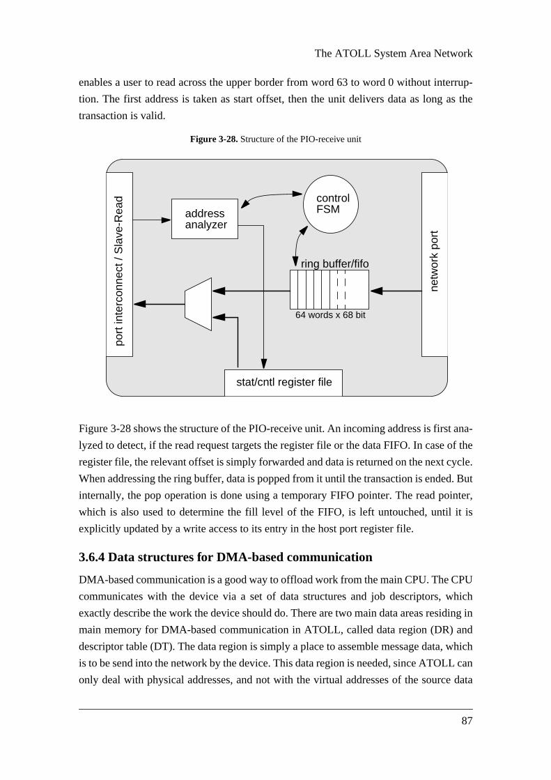
The ATOLL System Area Network
rrup-
as the
ana-
of the
ycle.
. But
inter,
t is
PU
hich
ing in
nd
which
L can
e data
enables a user to read across the upper border from word 63 to word 0 without inte
tion. The first address is taken as start offset, then the unit delivers data as long
transaction is valid.
Figure 3-28.Structure of the PIO-receive unit
Figure 3-28 shows the structure of the PIO-receive unit. An incoming address is first
lyzed to detect, if the read request targets the register file or the data FIFO. In case
register file, the relevant offset is simply forwarded and data is returned on the next c
When addressing the ring buffer, data is popped from it until the transaction is ended
internally, the pop operation is done using a temporary FIFO pointer. The read po
which is also used to determine the fill level of the FIFO, is left untouched, until i
explicitly updated by a write access to its entry in the host port register file.
3.6.4 Data structures for DMA-based communication
DMA-based communication is a good way to offload work from the main CPU. The C
communicates with the device via a set of data structures and job descriptors, w
exactly describe the work the device should do. There are two main data areas resid
main memory for DMA-based communication in ATOLL, called data region (DR) a
descriptor table (DT). The data region is simply a place to assemble message data,
is to be send into the network by the device. This data region is needed, since ATOL
only deal with physical addresses, and not with the virtual addresses of the sourc
address
netw
ork
port
port
inte
rcon
nect
/ S
lave
-Rea
d
stat/cntl register file
analyzer
ring buffer/fifo
64 words x 68 bit
controlFSM
87

Host port
ment,
for the
ary
ning,
sed to
load,
aths
event
made
ower
e data
ower
ion.
r each
ed to
e data
soft-
frame
64 bit
. Cur-
to 1
region
lity to
locations in the user’s virtual address space. Though this is not impossible to imple
as demonstrated by Quadrics QsNet, its complex implementation was abandoned
first version of ATOLL. So ATOLL needs a pinned-down memory area to tempor
buffer the message payload.
Figure 3-29.Data region
Figure 3-29 depicts the layout of a data region. A base address marks the begin
whereas an upper bound marks the end of the area. Read and write pointers are u
index into this region, which is used as ring buffer. In contrast to header and data pay
the routing information of a message is normally static. At system start, all routing p
to all other nodes are computed and remain fixed during the application run. So to pr
the copying of the same data again and again into the data region, the decision was
to provide a small static area to keep the routing table. This is done by defining a l
bound, which is used as next offset in case data hits the upper bound. Separat
regions exist for sending and receiving data, with the receiving data region lacking a l
bound. It is simply not needed, since incoming messages have no routing informat
The second data area is the descriptor table, which keeps fix-sized job descriptors fo
DMA message. The job descriptors consist of four 64 bit words. Three words are us
describe the three message frames, their offset relative to the base address of th
region and their length. The 4.word is an additional tag, which can be utilized by the
ware to distinguish between different protocols or message types.
Figure 3-30 shows the layout of a job descriptor. The offsets point to the associated
data, relative to the base address of the data region. Lengths are given in terms of
words. The upper byte of the routing length is used as an additional command byte
rently, only one special command is encoded. By setting the lowest bit of this byte
one can mark a job as non-consuming. This means that data is read from the data
as normal, but the read pointer is not advanced afterwards. This offers the possibi
routing table
free
header/data
DR base addr
lower bound
upper bound
read ptr
write ptr
free
88

The ATOLL System Area Network
ending
ltiple
is byte
current
vent
sage
E.g.,
mode,
ords.
nd the
these
ree up
do not
file. It
d and
d and
. Most
ransfer,
base
base
reference the data again. This method can be used to implement broadcasts on the s
side by copying the payload just once into the data region and referencing it with mu
descriptors.
Figure 3-30.Job descriptor
The command byte is used on the sending side only. When receiving a message, th
is used as a status byte to flag special events associated with the message. In the
version of ATOLL, only the lowest bit is used to mark incomplete messages. This e
occurs, when the number of words received from the network differs from the mes
length information, which is always at the start of the header frame of a message.
this can occur, when a user process core dumps while sending a message in PIO
and the driver software completes the message, but not with the right number of w
Similar to the data region, there are separate descriptor tables for the DMA-send a
DMA-receive units. As described earlier, a host port generates an interrupt when
resources are exhausted on the receiving side. Driver software should then always f
a large amount of memory space to make sure that messages waiting to be received
block the network.
3.6.5 Status/control registers
The status/control registers needed for a host port are stored in a separate register
interfaces with all other components of a host port to gather the status data neede
spreads out the control information to the units. A separate page is used for the sen
the receive part, but only nearly a dozen of registers are implemented for each page
of them store the base addresses and offsets needed for DMA-based message t
whereas only a few are needed to control the PIO mode.
Table 3-5 lists all registers of the send page. The offsets are relative to the page
address. All registers are 64 bit words, but not all bits might be relevant. Only the
routing:
header:
data:
offset length
tag
cmdbyte
03163 23
offset
offset
length
length
89

Host port
PIO-
me as
.
reg-
the
global
It is
addresses occupy all 64 bits, the other offsets are 32 bit wide. And the fill level of the
send FIFO fits into the lower 6 bits of the associated register.
Table 3-6 lists all registers of the receive page. The DMA registers are almost the sa
for the send page, except the unnecessary lower bound register for the data region
Besides the fill level of the PIO-receive data FIFO, the receive page also includes a
ister for the FIFO read pointer. Writing a new value to it is equivalent to shifting out
previously read data words. Each host port has also read access to the internal
counter, which is located in the supervisor initialization registers described earlier.
Table 3-5.Send status/control registers of a host port
register name offset mode, width comment
snd_DT_base 0000h r/w, 64 base address of the DT
snd_DT_read_ptr 0008h r/w, 32 read pointer of the DT
snd_DT_write_ptr 0010h r/w, 32 write pointer of the DT
snd_DT_upper_bound 0018h r/w, 32 upper bound of the DT
snd_DR_base 0020h r/w, 64 base address of the DR
snd_DR_lower_bound 0028h r/w, 32 lower bound of the DR
snd_DR_read_ptr 0030h r/w, 32 read pointer of the DR
snd_DR_write_ptr 0038h r/w, 32 write pointer of the DR
snd_DR_upper_bound 0040h r/w, 32 upper bound of the DR
snd_repl_base 0048h r/w, 64 base address of the replicator
snd_fifo_fill_level 0800h ro, 6 fill level of the PIO-send data FIFO
Table 3-6.Receive status/control registers of a host port
register name offset mode, width comment
rcv_DT_base 0000h r/w, 64 base address of the DT
rcv_DT_read_ptr 0008h r/w, 32 read pointer of the DT
rcv_DT_write_ptr 0010h r/w, 32 write pointer of the DT
rcv_DT_upper_bound 0018h r/w, 32 upper bound of the DT
rcv_DR_base 0020h r/w, 64 base address of the DR
rcv_DR_read_ptr 0028h r/w, 32 read pointer of the DR
rcv_DR_write_ptr 0030h r/w, 32 write pointer of the DR
rcv_DR_upper_bound 0038h r/w, 32 upper bound of the DR
rcv_fifo_fill_level 0800h ro, 6 fill level of the PIO-receive data FIFO
rcv_fifo_read_ptr 0808h r/w, 6 read pointer of the PIO-receive data FIFO
semaphore FC00h r/w, 64 semaphore, set on read as side effect
cnt FE00h ro, 64 global counter
90

The ATOLL System Area Network
ertain
se the
t the
ut it
ccess
value
g a 0
lue, all
others
and to
the
data is
ows
ppli-
by
on-
simply spread out to all host ports, so user applications can e.g. precisely time c
ATOLL library calls.
Another special feature is the semaphore register. It is intended to be utilized in ca
host port needs to be multiplexed between several applications. This is normally no
case for production-type clusters, since performance is degraded significantly. B
might make sense for application development or debugging purposes. A write a
simply writes the specified data to the register. But a read access returns the stored
and, as side effect, sets all bits to 1. So one could initialize the semaphore by writin
to it. When several user processes try to read the register, only one gets the 0 as va
others see all bits set to 1. So the one with the 0 has acquired the semaphore, all
must wait, until the locking application frees it by writing a 0 back to the register.
3.6.6 DMA-send unit
Figure 3-31.Control flow of sending a DMA message
The DMA-send unit is responsible to observe the data areas for sending messages,
process all valid entries in the send descriptor table. If a job is available, it loads
descriptor, and subsequently loads all message frame data. As soon as requested
returning from the PCI-X interface it is forwarded to the network port. Figure 3-31 sh
the general control flow of sending a message via the DMA mode, for both the user a
cation and the DMA-send unit. The application triggers the DMA-send control logic
writing new values of the write pointers for DT & DR into the host port. These are c
write header & datato data region
create new job descriptorin descriptor table
update DT & DR writepointers in host port
write data
write desc.
trigger host port
application DMA-send unit
load the job desc.from DT
load desc.
load all 3 frames from DRand forward it to network
load message
update DT & DR readpointers in host port
free memory
91

Host port
riptor
gns.
n’ in
trans-
gned a
f the
usly
y and
load
of jobs
ushed
arbi-
m with
tinuously monitored by the host port. As soon as read and write pointers of the desc
table are unequal, a valid job entry is present and processed.
Figure 3-32.Structure of the DMA-send unit
Figure 3-32 depicts the structure of the DMA-send unit. It is split up into two subdesi
One part is responsible for requesting data from memory, labeled with ‘job creatio
the figure. As described earlier, the Master-Read interface implements a split phase
action scheme, where blocks of up to 32 words can be requested. Each job is assi
unique ID, with up to 8 jobs in progress. The ‘job creation’ part now keeps copies o
relevant status/control registers in a working set module. This working set is continuo
updated from the status/control register file of the host port.
As soon as an entry is detected in the descriptor table, it is requested from memor
stored in the working set. Step by step the ‘job creation’ part now computes the
addresses from fixed base addresses and the offsets given in the descriptor. A set
is then generated to fetch all frame data from memory. The associated job IDs are p
into a job queue. This is necessary since multiple host ports might request data in an
trary sequence. So each host port must keep the jobs it has requested to match the
the ID of returning jobs.
working set
netw
ork
port
port
inte
rcon
nect
/ M
aste
r-R
ead
64x68 data fifo
reg fileaddresscalculation
+
control FSMload desc., datacntl interface
job creation
job completionst
at/c
ntl r
eg fi
le
8x10
b fif
o
job
queu
e
send fifo
control FSMmonitor job queuetransfer data
=
92

The ATOLL System Area Network
other
es it
nding
ort. If
up to
to be
n also
cupied
from
ory.
nsists
in a
data
emory.
ppli-
es-
The second part is called ‘job completion’ and is responsible to accept the data the
part has requested. It therefore monitors the IDs of incoming jobs to detect the on
should process. Incoming data is then placed in a FIFO, marked with its correspo
tags. As soon as data is in the FIFO, this part requests access to the network p
granted, data is transferred towards the network. Since the FIFO can only store
64 words, the unit cannot request more data. Doing so could cause all data paths
blocked in case the path towards the network is not available. This can happen whe
the PIO-send unit is transferring a message, or the path through the crossbar is oc
by a message just passing through the ATOLL chip.
3.6.7 DMA-receive unit
Figure 3-33.Control flow of the DMA-receive unit
The DMA-receive unit is the counterpart to the DMA-send unit. It gets message data
the network port and spools this data out to the DMA data structures in main mem
Figure 3-33 shows the main control sequence of the unit. An incoming message co
of the header and the data frame, since the routing frame is no more needed.
Similar to the DMA-send unit, the DMA-receive module keeps the relevant registers
small working set. It then writes header and data out to memory. After all message
has been processed, it assembles a descriptor pointing to the data spooled out to m
This job descriptor is then stored in the receive DT, which is monitored by the user a
cation. The write pointers of both DT & DR are updated to reflect the newly arrived m
sage.
DMA-receive unit
spool header out to.memory
store header
spool data out to memory
store data
write desc. to DTupdate write ptrs
store desc.
93

Host port
ing
gister
f the
ble to
it gen-
nt read
ltiple
soon
to the
Only
tercon-
bility
uld
regis-
ion of
Figure 3-34.Structure of the DMA-receive unit
Figure 3-34 gives an overview about the structure of the DMA-receive module. Incom
data is first stored in a FIFO. Addresses are computed for each data word from the re
values of the working set. Prior to handing data over to the Master-Write interface o
port interconnect, the control logic makes sure, that enough memory space is availa
store the message in the DMA-receive data structures. If this is not the case, the un
erates an interrupt and waits, until software frees up memory and updates the releva
pointers of DT & DR.
Though each data word is transferred with its address, it makes no sense to mix mu
data streams from several active DMA-receive units on a word-by-word basis. So as
as data enters the FIFO from the network side, the unit requests exclusive access
port interconnect. If granted, it keeps the request up until no more data is available.
then the request is deasserted, and other host ports might get access to the port in
nect. This way a strong fragmentation of the data stream is avoided, with the proba
to assemble larger burst transfers.
3.6.8 Replicator
The replicator is used to avoid polling status registers of the ATOLL device, which co
degrade overall system performance by interfering with data transfer bursts. Those
ters needed by application software are automatically written out to a separate port
working set
netw
ork
port
port
inte
rcon
nect
/ M
aste
r-W
rite
64x68 data fifo
reg file
addresscalculation
+
stat
/cnt
l reg
file
receive fifo
control FSMcheck spacetransfer data
94

The ATOLL System Area Network
s of
of all
addi-
s the
ory.
e asso-
base
read-
t-up).
s also
bed in
hile
value
ade
ide
pdates
data
d the
one.
has
ld into
main memory. There are 8 registers in total written out, separated in two group
4 registers, one for send and one for receive operations. An update consists
4 registers of each block. New register values are handed over to the replicator, and
tional trigger signals force it to update the values in memory.
The replicator utilizes the same Master-Write interface of the port interconnect a
DMA-receive unit. Table 3-7 shows the layout of the mirrored registers in main mem
Each host port can be assigned a unique base address for its replicator through th
ciated register in its control/status register file. The offsets given are relative to this
address. Though located in normal main memory, those locations are declared as
only, since they should not be altered by software (except initialization at system star
The read and write pointers of the DMA modes are updated on each change. This i
true for the semaphore and the read pointer of the PIO-receive FIFO. But as descri
previous sections, the update frequency of the FIFO fill level can be configured. So w
utilizing these registers in the replication area one must keep in mind, that the real
might differ from the mirrored one by up to the threshold value. E.g., if an update is m
every 8 words and the mirrored FIFO fill level is 32, then the real FIFO fill level ins
the host port can be in the range 25-39. And even worse, there can be pending u
waiting to be transferred to main memory in the device. This might happen if the
paths are congested due to multiple active host ports.
So before interpreting the value in the replication area, an application should rea
value directly from the device once to make sure, that it is the same as the mirrored
And while doing calculations with these values, e.g. to check if the PIO-send FIFO
enough space left for a message to send, the software should take the thresho
account.
Table 3-7.Layout of the replicator area
register name offset mode, width comment
snd_DT_read_ptr 0000h ro, 32 read pointer of the send DT
snd_DR_read_ptr 0008h ro, 32 read pointer of the send DR
snd_fifo_fill_level 0010h ro, 6 fill level of the PIO-send data FIFO
semaphore 0018h ro, 64 current semaphore value
rcv_DT_write_ptr 0020h ro, 32 write pointer of the receive DT
rcv_DR_write_ptr 0028h ro, 32 write pointer of the receive DR
rcv_fifo_fill_level 0030h ro, 6 fill level of the PIO-receive data FIFO
rcv_fifo_read_ptr 0038h ro, 6 read pointer of the PIO-receive data FIFO
95

Network port
wide
nto
tween
rt also
data.
n, so
nsists
are
st one
pro-
used
itional
data:
3.7 Network port
The network port is converting the tagged data stream of 64 bit words into a byte-
stream according to the link protocol defined for ATOLL and vice versa. It is split i
two separate units for sending and receiving messages. There is no interaction be
those two units, so they both can process messages concurrently. The sending pa
generates CRC values for error detection later in each network stage.
3.7.1 Message frames and link protocol
As stated earlier, an ATOLL message consists of three frames: routing, header and
The routing frame is consumed while the message is routed towards its destinatio
only header and data frame enter the receiving path of a network port. Each frame co
of several link packets, which can consist of up to 64 data bytes. Only full 64 words
used to form a message, so the number of data bytes is always a multiple of 8. At lea
data word must be in every frame to ease the implementation.
Figure 3-35.Message frames
Figure 3-35 gives an overview about the framing of ATOLL messages and the link
tocol used for the byte-wide data stream in the network. Separate control bytes are
to enclose the normal message data bytes and to ensure a correct framing. An add
ninth bit is used to distinguish between control and data bytes (0 = data, 1 = cntl).
There are 4 control bytes used at the network port to build up the framing of message
• SOF (Start Of Frame) is the 1.byte of a new frame
message:
routingframes:
SOP
header data
R H D
EOM
CRCEOP... R SOP ... H EOP
H CRC... H EOP
SOP D... EOP
D D...multiple link packetsper frame possible
frames start witha SOP byte
the last link packetends with an EOM byte
CRC bytes protectmessage data
H H D D
CRC
CRC
96

The ATOLL System Area Network
is
EOP
t react
ting
e that
bytes
con-
sage,
e tag.
uton-
, this
ld. The
IO-
• a CRC value is computed for each link packet in the header and data frames. It
appended to the end of the link packet
• EOP (End Of Packet) marks the end of a link packet
• EOM (End Of Message) marks the end of the whole message, and replaces the
byte of the last link packet
Link packets in the routing frame do not have a CRC value attached, since one mus
on bit errors in routing bytes immediately. This is handled by using an error detec
code for routing bytes, which is discussed in detail later on.
Each frame can be composed of several link packets, but the normal case should b
a single link packet is enough for the routing and the header frame. E.g., 64 routing
are sufficient to define routing paths in a 2D grid of 32 x 32 = 1024 nodes. A special
straint exists for the header frame. The 1.word of it must be the length of the mes
given as separate 32 bit values for header and data frame. The 2.word must be th
This is necessary to give the host port at the receiving side the possibility to check a
omously, if the message should be received in PIO or DMA mode. As stated earlier
decision is made based on the length of the message and a configurable thresho
DMA-send unit automatically ensures this constraint, but e.g. software utilizing the P
send mode has to take care of this constraint, too.
3.7.2 Send path
Figure 3-36.Structure of the send network port unitcr
ossb
ar
host
por
t
8x68 data fifo
data
input fifo
control FSM
ensure protocol
16x9 data fifo
output fifoconversion
64 b
it
9 bi
t
CRCgenerator
97

Network port
n be
e. The
small
ms a
o the
pro-
ed and
ta is
ross-
cally
posite
s off
ords.
ppens
64 bit
s.
ight
ng the
ontrol
these
or, the
Figure 3-36 depicts the overall structure of the send unit of the network port. It ca
viewed as a 3-stage pipeline consisting of an input, a processing and an output stag
host port delivers a stream of tagged 64 bit words. This data is temporary stored in a
FIFO. The following processing stage now shifts out the data word by word and for
stream of bytes, tagged with the cntl/data flag bit. It inserts control bytes according t
link protocol where necessary. A CRC generator computes the CRC value of the
cessed data. After a full link packet has been processed, this CRC value is append
the link packet is completed by an EOP or EOM control byte. This stream of link da
pushed into an output FIFO, which keeps the data until it is transferred towards the c
bar.
3.7.3 Receive path
Figure 3-37 shows the structure of the receive unit inside the network port. It basi
consists of the same 3-stage processing pipeline as the send part, but only in the op
direction. Data assembles in a small input FIFO. The following protocol stage strip
the control bytes from the link data stream. It rebuilds a stream of tagged 64 bit w
There might be some unused routing bytes left at the head of the message. This ha
e.g. when only 3 network hops are needed. Since frames are made of multiple
words, 5 bytes are unused. These are simply dropped until the header frame begin
Figure 3-37.Structure of the receive network port unit
The output stage is a bit more complex than in the send unit. Incoming link packets m
be marked as corrupted, since transmission errors were discovered somewhere alo
path the message took through the network. These packets end with a special error c
byte EOP_ERR (End Of Packet ERRor), instead of the normal EOP byte. Since
packets are automatically retransmitted to the network stage which detected the err
cros
sbar
host
por
t
8x68 data fifo
dataoutput fifo 0
control FSMstrip link protocol
8x9 data fifo
input fifo
conversion
64 b
it
9 bi
t
check CRC8x68 data fifo
output fifo 1
fifo cntlmultiplexfifos
98

The ATOLL System Area Network
acket
shed
ption
ince
, since
f erro-
r and
n each
the
port
again
utput
ed in
in the
the
en
e of
t. An
esolve
ssbar
age
includ-
same link packet follows the corrupted one in the data stream. So the corrupted link p
needs to be filtered out at the receive unit of the network port. This means data pu
into the output stage cannot be forwarded to the host port prior to the complete rece
of a correct link packet.
Providing only one output FIFO would result in a significant performance penalty, s
the data stream would be repeatedly stopped and restarted. This would happen
pushing data into the FIFO and popping data from it cannot be overlapped. In case o
neous link packets one would otherwise need to keep track of which words to transfe
which ones to delete.
To keep data flowing a second FIFO was implemented, and the data path switches o
link packet between them. This way, the normal operation of this unit is as follows:
• a link packet is processed and pushed into FIFO 0
• after making sure it is valid, the next incoming packet is pushed into FIFO 1 and
control logic of the output stage is ordered to forward the data in FIFO 0
• while the second link packet is processed, the first one is transferred to the host
• after finishing the second packet, FIFO 0 is empty again and roles are switched
Simulations showed a significant gain in sustained throughput of the unit using two o
FIFOs instead of just one. In case of only one FIFO, a few wait cycles were introduc
the network port. But even more serious was that these short periods of blockages
data stream triggered the flow control of previous links, causing larger idle times on
links along the data path.
3.8 Crossbar
The crossbar [69]1 is a full-duplex 4x4 switch, providing an all-to-all connection betwe
the 4 network ports on one side and the 4 link ports on the other side. It is mad
8 identical crossbar ports, which again are split up into an input and an output uni
additional debug interface observes the status of the crossbar and can be utilized to r
major failures, like deadlocks or misrouted messages. The overall structure of the cro
is shown in Figure 3-38.
The input unit of a crossbar port strips off the first routing byte of an incoming mess
and sets the request for the addressed crossbar port. This can be any of the 8 ports,
1. designed and implemented by Prof. Dr. Ulrich Brüning and Jörg Kluge
99

Crossbar
il the
ut unit
es other
hion.
If the
ross-
sed via
The
nd the
are
ing itself. It then waits for the other side to grant the access and forwards data, unt
end of the message is reached. To not monopolize a specific crossbar port, each inp
deasserts a request for at least 3 cycles between back-to-back messages. This giv
ports a chance to request the port.
Figure 3-38.Structure of the crossbar
The output unit of a crossbar port arbitrates its data path in a fair round-robin fas
Once a request is served, data flows into the unit and is buffered in a small FIFO.
following unit signals its ability to accept data, the message is transferred out of the c
bar. All interfaces use the two-way handshaking introduced earlier.
The additional debug interface observes the status of the crossbar and can be acces
the debug registers listed in “ATOLL control and status registers” on page 71.
detailed implementation of the crossbar and the use of the debug interface is beyo
scope of this document. Further information can be looked up in the ATOLL Hardw
Reference Manual [67].
link
netw
ork
xbar port 0
port
0ne
twor
kpo
rt 1
netw
ork
port
2ne
twor
kpo
rt 3
port
0lin
kpo
rt 1
link
port
2lin
kpo
rt 3
input
output
debuginterface
xbar port 1
input
output
xbar port 2
input
output
xbar port 3
input
output
xbar port 4
input
output
xbar port 5
input
output
xbar port 6
input
output
xbar port 7
input
output
all-t
o-al
l sw
itch
mat
rix
100

The ATOLL System Area Network
r the
e-
error-
uffer
n-
other
on is
ntro-
envi-
iffer-
sses:
yte is
at the
net-
false
uting
rmal
ing
ulty
am
any
ytes.
ts the
3.9 Link port
The link port is the gateway to the network. It directly drives and receives signals ove
link cables. As all other top-level building blocks of ATOLL, it is also split up into ind
pendent units for sending and receiving data. Its main task is to ensure proper and
free transmission of data. This includes a reverse flow control protocol to prevent b
overflow on the receiving side in case of blocked data paths.
A unique feature of an ATOLL link is its per-link error detection and correction. In co
trast to the end-to-end error detection and software-driven retransmission found in
networks, ATOLL link packets are checked in each network stage. Retransmissi
completely handled by hardware and occurs immediately on the link the error was i
duced. This provides an extremely fast way to solve the issue of rare bit errors due to
ronmental influences on the link cables.
3.9.1 Link protocol
Two types of bytes make up the link data stream: data and control bytes. They are d
entiated by an additional ninth bit. Data bytes itself can be separated into two cla
routing bytes and normal payload bytes for the header and data frames. A routing b
special, since it carries the information of the output port its message should take
next crossbar. A bit error in a routing byte would result in catastrophic failure of the
work. The message would take a different path then specified, causing it to arrive at a
destination, or even worse, let it end somewhere in a network stage due to missing ro
information. So one must react immediately in case of errors in routing bytes, the no
CRC link packet protection scheme of the other two frames is useless here.
Therefore, the upper bit of a routing byte is a parity bit calculated from the remain
7 bits. This offers the opportunity to detect a single-bit error immediately. Such a fa
bit is replaced with a special CANCEL control byte, signalizing all other downstre
units that this routing link packet is to be ignored. It is then retransmitted just like
other erroneous link packet.
Table 3-8 gives an overview about the format and encoding of all data and control b
The first two rows show the encoding of normal data and routing bytes, whereby bitd[8]
is the bit distinguishing between data and control bytes. The rest of the table depic
encoding of all 11 control bytes used in the ATOLL link protocol.
101

Link port
thod
is an
e fly.
ply
. The
ver a
and
link
Since only data bytes are protected by link packet CRCs or parity bits, another me
had to be found for the control bytes. They are protected by a hamming code, which
error correcting code (ECC). So an error is not only detected, but also corrected on th
This is accomplished by using 3 bits of the byte as parity bits, marked asp[2:0] in the
table. The parity bits are encoded as follows:
p[0] = XOR(d[6], d[4], d[2])
p[1] = XOR(d[6], d[5], d[2])
p[2] = XOR(d[6], d[5], d[4])
Using this hamming code, a correct control byte can be identified byp[2:0] = 000. Any
nonzero value of the parity bits points to the erroneous bit position, which is then sim
inverted to correct a single-bit error. E.g. a value of011 for the parity bits identifies bit
d[2] as incorrect.
The control bytes SOF, EOM, EOP, EOP_ERR and CANCEL were described earlier
IDLE byte is simply used as filler, since a byte is transmitted on each clock edge o
link. STOP and CONT are the bytes used for the reverse flow control. POSACK
NEGACK are used by a receiving link port to signal the sender a good or a bad
packet. The RETRANS byte is used to lead any retransmitted link packet.
Table 3-8.Encoding of data and control bytes
hex d[8] d[7] d[6] d[5] d[4] d[3] d[2] d[1] d[0] comment
0xx 0 - - - - - - - - normal data byte
0xx 0 par - - - - - - - routing byte with parity bit
d[5] d[4] d[3] d[2] d[1] p[2] d[0] p[1] p[0] ECC bit positions, hamming code
1FF 1 1 1 1 1 1 1 1 1 IDLE (filler byte)
100 1 0 0 0 0 0 0 0 0 SOF (Start Of Frame)
107 1 0 0 0 0 0 1 1 1 EOM (End Of Message)
119 1 0 0 0 1 1 0 0 1 EOP (End Of Packet)
11E 1 0 0 0 1 1 1 1 0 EOP_ERR (End Of Packet ERRor)
12A 1 0 0 1 0 1 0 1 0 STOP (STOP sending of data)
12D 1 0 0 1 0 1 1 0 1 CONT (CONTinue sending data)
133 1 0 0 1 1 0 0 1 1 POSACK (POSitive ACKnowledge)
134 1 0 0 1 1 0 1 0 0 NEGACK (NEGative ACKnowledge)
14B 1 0 1 0 0 1 0 1 1 RETRANS (RETRANSmit link packet)
14C 1 0 1 0 0 1 1 0 0 CANCEL (CANCEL routing)
102

The ATOLL System Area Network
t up
ssage
now
ink. If
acket.
cable
link
store
n be
offer-
mall
uffers
3.9.2 Output port
Figure 3-39.Structure of the output link port
Figure 3-39 gives an overview about the structure of the link port output unit. It is spli
into 4 areas according to the different tasks it should manage. The input path gets me
data from the crossbar and stores it temporary in a small input FIFO. Control logic
forwards each link packet towards the output path, storing data in another FIFO.
The retransmit path is responsible to keep a copy of each link packet sent over the l
the receiving side signals a corrupted packet, this unit can retransmit the erroneous p
Since the acknowledge from the other side has a certain delay (error detecting logic,
propagation time), it would be a waste of bandwidth to wait for it after each single
packet. So the retransmit path has two identical retransmit buffers to be able to
2 packets in parallel.
During the unit waits for the acknowledgment of the first packet, a second one ca
transmitted. Thus transmission and acknowledgment of link packets is overlapped,
ing the possibility to operate the link at full capacity. Sometimes it happens that s
packets are transferred, e.g. routing or header packets with only 1-2 words. If both b
cros
sbar
8x9 fifo
input fifo
8x9 fifo
output fifo
cntl FSM
68x9 fifo
retrans buf0
68x9 fifo
retrans buf1
cntl FSM
reverse flowcntl insertion
link
cabl
e ou
t
output patharbiter
input path
retransmit path
rev. flow cntl path
output path
103

Link port
long
into
head
n to
of
e FIFO
nism
sts to
erse
trol
cess
are filled and wait for their corresponding acknowledge, the input path is stopped as
as one of the buffers is free again.
Figure 3-40.Reverse flow control mechanism
Figure 3-40 shows how the reverse flow control path is utilized to insert control bytes
the opposite data stream of a full-duplex link:
• A: the FIFO on the receiving side runs full, because the path is blocked further a
• B: the input path requests its associated output path to send a STOP signal
• C: the STOP byte is inserted into the data stream on the opposite path of a link
• D: the input path of the sender filters out the STOP byte and signals its receptio
the output path
• E: the sending output path recognizes the STOP request and stops transmission
message data. Instead, it sends only IDLE fillers
The same procedure happens in case the blockage of the path is removed and th
can again store data. This is signaled by sending a CONT control byte. This mecha
is also used for the acknowledgment of link packets. The checking input path reque
send a POSACK or NEGACK byte, which is filtered out at the other side. So the rev
flow control path of the output unit is responsible for the insertion of these four con
bytes into the link data stream. Additional arbiter and datapath logic multiplex the ac
to the link cable between the three subunits of the output path.
link port
input path
output path
node 0 node 1link port
input path
output path
fifo runsfull!
A
B
C
D
request tosend a STOP
ST
OP
IDLE
IDLE ......
a STOP is sentto the sendinglink port
STOP issignaled
IDLE
IDLE
IDLE... ...
sender stopstransfer of data,sends fillers
E
104

The ATOLL System Area Network
wed
rage.
ize
used
ction
push
pre-
at at
need
uting
ing
an be
t. This
gic,
link
en it is
the
gh to
send
3.9.3 Input port
Figure 3-41.Structure of the input link port
The structure of the input path of the link port is shown in Figure 3-41. It can be vie
as a pipeline of 3 stages: data synchronization, error checking & decode and sto
Since all ATOLL chips have their own internal clock signal, one must first synchron
the incoming data to the clock of the receiving node. An additional tenth signal line is
in the cable to transfer the clock. This is done at half the rate to prevent the introdu
of noise onto the data wires. This clock signal is now recovered by a PLL and used to
data into a dual-clock data FIFO. Only non-ILDE bytes are pushed into the FIFO to
vent an overflow by a slightly faster running sender. The output port makes sure, th
least 1 IDLE byte is sent per 64 byte link packet.
The second stage decodes all control bytes and filters out flow control signals, which
to be forwarded to the corresponding output path (STOP, CONT, etc.). It checks ro
bytes for parity errors, possibly corrects bit errors of control bytes by using the hamm
code, and checks the CRC of link packets. For debugging purposes, a multiplexer c
used to choose between the data from the cable and the data sent out by the link por
offers the possibility to run the link port in a kind of loopback mode.
Finally, data is pushed into a large FIFO. This FIFO is observed by some control lo
which triggers the sending of STOP and CONT control bytes to stop and restart the
data stream. The FIFO can store up to 256 bytes, and the data stream is halted, wh
filled to 50 %. For a short period of time data is still coming into the link port, since
request needs some time to arrive at the opposite side. This configuration is enou
support links of up to 25 m. Falling again under the 50 % mark triggers the request to
a CONT byte.
link
cabl
e in
cros
sbar
control FSM
16x9 data fifo
synch fifo
PLLlink clkrecovery
256x9 data fifo
input fifo CRC check& decode
Fifo statusobservation
105

Link port
106

Implementation
Cir-
level
om-
ly be
vity
ncial
f this
team
as
final
g the
ly
type
-art
UMC,
ost
also
and
rar-
es
l with
ce in
n very
r the
4Implementation
The implementation of the ATOLL architecture as an Application Specific Integrated
cuit (ASIC) [70] has been a huge challenge. With the complexity and the aggressive
of integration, the task of implementing the ATOLL chip is comparable to high-end c
mercial chip developments at major semiconductor companies. The goal could on
attained by following a carefully planned project schedule, maximizing the producti
of the manpower at our disposal. Other big hurdles have been the restricted fina
budget and the limited access to chip development tools. Normally, ASIC projects o
size are heavily supported by the technology and tool vendors to help the design
solving critical issues. The available support from this side for the ATOLL project w
very limited. But despite all these obstacles, the design team was able to ship the
transistor layout to production in February 2002, almost 3 years after implementin
first simulation modules.
The Europractice IC Service1, which is funded by the European Union (EU), is normal
the only way for European research labs and universities to fabricate a few proto
chips to validate the practicability of their ideas. The only available state-of-the
CMOS process at the time the project was planned was the 0.18 um process from
Taiwan. So this technology has been chosen for the implementation of ATOLL. M
Electronic Design Automation (EDA) tools used for the chip development were
acquired via Europractice. Almost all the tools are developed by Synopsys, Inc.
Cadence Design Systems, Inc., two of the leading EDA companies.
The ATOLL ASIC is a standard cell based design. Using such pre-configured cell lib
ies, containing logic gates like AND, OR, NAND, NOR, NOT, DFF, etc. in different siz
with several driving strengths, speeds up the design time, since one has not to dea
traditional VLSI design techniques. But the disadvantage is the loss of performan
terms of speed and greater power consumption, since these cell libraries are ofte
conservative to ensure proper function in silicon. Europractice offers such a library fo
UMC process from Virtual Silicon Technologies, Inc. (VST).
1. www.europractice.imec.be
107

Design Flow
only
ells.
n
the
uency
h end
faster
Syn-
tools
hase.
, addi-
pro-
ach
almost
rther
, Bel-
in the
To concentrate on the development of the logic unique to ATOLL, several comm
used building blocks were integrated by using external Intellectual Property (IP) c
These cells are:
• a PCI-X interface, donated by Synopsys
• DFF-based fifo structures, included in the DesignWare IP library from Synopsys
• RAMs of different sizes, generated by a RAM compiler from VST
• two kinds of PLLs, generated by a PLL compiler from VST
• three special full-custom I/O cells (PCI-X, LVDS-IN, LVDS-OUT), developed by a
analog expert team from the University of Kaiserslautern
4.1 Design Flow
The design flow [71] pretty much follows the standard ASIC design flow used over
last decade to design digital ICs. The size of the design and its aggressive target freq
would have been better manageable with some of the new EDA tools targeting hig
designs. These new tools merge the logical and physical design steps, providing a
implementation and more predictable results. Examples are Physical Compiler from
opsys and Physically Knowledgeable Synthesis (PKS) from Cadence. But these
were not part of the Europractice tool packages at the start of the implementation p
Cadence PKS tools have been made available lately, though.
So a design flow had to be established from the accessible tools. Where necessary
tional tools, e.g. for design entry and HDL linting, were acquired to further enhance
ductivity, if affordable. Figure 4-1 depicts the overall design flow, the tools used for e
step and the design formats exchanged between them. Since the design team had
no knowledge of backend design (placement & routing of standard cells) and to fu
reduce the workload, it was chosen to draw on the backend service offered by IMEC
gium for Europractice customers. Each of the illustrated steps is described in detail
following sections.
108

Implementation
nsfer
rate
m the
efine-
back
of logic
erging
Figure 4-1.ATOLL design flow
4.2 Design entry
The whole design has been implemented using the Verilog HDL on Register-Tra
Level (RTL). This is achieved by specifying the behavior of the logic in a cycle-accu
manner. The design process followed a mixed bottom-up, top-down approach. Fro
top-level of the chip, a hierarchy of modules has been implemented. A step-by-step r
ment of module interfaces and the logic inside functional units has given early feed
on the consequences of design decisions and sometimes led to the rearrangement
for better performance. Other modules have been designed the same time by m
basic functional units into larger and more complex blocks.
design entry/RTL coding
functionalsimulation
logic synthesis
test insertion
floorplanningplace & route
gate-levelsimulation
IPO/ECOoptimization
tape outto UMC
Verilog HDLHDL Designer (Mentor): design entryVerification Navigator (TransEDA): HDL linting
NC-Sim (Cadence): Verilog simulation
Design Compiler (Synopsys): logic synthesisPrimetime (Synopsys): static timing analysis
DfT Compiler (Synopsys): scan insertionBSD Compiler (Synopsys): boundary scan (JTAG)TetraMAX (Synopsys): ATPG
Apollo II (Avant!): floorplan, place & routeStar-RCXT (Avant!): parasitic extraction
Floorplan Manager (Synopsys):post-layout optimization
NC-Sim (Cadence): Verilog simulation
Verilog RTL
Verilog netlist
SDF, PDEF
GDSII
set_load
Verilog RTL
Verilog netlist
Verilog netlist
Verilognetlist
SDF: Standard Delay FormatPDEF: Physical Design Exchange Formatset_load: net capacitancesGDSII: polygon layer masks
109

Design entry
n was
es, the
tion
code)
een uti-
y to
M),
code
ntrol
more
und
were
e. In
s used
SMs
ign
which
writ-
hich
ecial
a-
and
linter.
ally
ethod,
e.
I-X,
ain
To deal with the large design hierarchy and to enhance its visualization, the decisio
made to use a schematic-based design entry tool. After evaluating several alternativ
HDL Designer Series from Mentor Graphics was chosen. It offers good visualiza
opportunities, multiple entry formats (schematics, state machines, truth tables, HDL
and team-based design management. Its RCS-based version management has b
lized to prevent conflicting modifications to the design, as well as to provide the abilit
fall back to previous versions of modules.
For an efficient implementation of complex control logic as Finite State Machines (FS
a custom developed tool called FSMDesigner [72] has been used. Its optimized HDL
generation proved to be a valuable help to deal with complex, hard to implement co
logic. The most obvious advantage was to be able to debug control logic at the
abstract level of FSMs, compared to plain HDL code. This provided a fast turnaro
time while debugging the design. Regarding the fact that most of the functional bugs
discovered in the control part of a unit, this helped to save weeks of development tim
a late stage of the design, the state machine editor of the HDL Designer Series wa
instead, after having figured out how to apply our special implementation style for F
to it.
4.2.1 RTL coding
Since the level of expertise in writing Verilog RTL code varied a lot inside the des
team, a way had to be found to make sure that all designers produce quality code,
could be easily merged into the whole design. A set of rules and guidelines [73] for
ing Verilog code was established, similar to the Reuse Methodology Manual [74], w
is widely used in industry. To automate the compliance checking of the code, a sp
HDL linting tool was acquired, called VN-Check. This tool is part of the larger Verific
tion Navigator (VN) tool suite from TransEDA. A rule database was implemented
each time a designer wanted to check in new code, it was first passed through the
This proved to be a fast and efficient way to catch a lot of coding errors, which norm
cause problems later in the flow. E.g., it ensured a consistent clocking and reset m
avoided unwanted latches, and forced designers to follow a consistent naming styl
4.2.2 Clock and reset logic
Besides the implementation of the architecture, the clock and reset logic1 of an ASIC is
always a critical factor. The whole chip integrates 6 different clock domains: PC
ATOLL and 4 link domains. The PCI-X clock is generated by logic on the host m
1. designed and implemented by Patrick Schulz for ATOLL
110
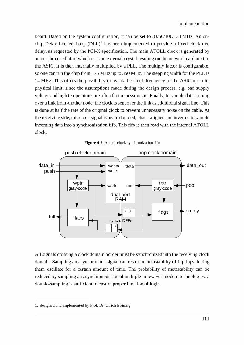
Implementation
n on-
ee
d by
xt to
e,
L is
its
upply
ming
This
le. At
ample
LL
lock
tting
be
ies, a
board. Based on the system configuration, it can be set to 33/66/100/133 MHz. A
chip Delay Locked Loop (DLL)1 has been implemented to provide a fixed clock tr
delay, as requested by the PCI-X specification. The main ATOLL clock is generate
an on-chip oscillator, which uses an external crystal residing on the network card ne
the ASIC. It is then internally multiplied by a PLL. The multiply factor is configurabl
so one can run the chip from 175 MHz up to 350 MHz. The stepping width for the PL
14 MHz. This offers the possibility to tweak the clock frequency of the ASIC up to
physical limit, since the assumptions made during the design process, e.g. bad s
voltage and high temperature, are often far too pessimistic. Finally, to sample data co
over a link from another node, the clock is sent over the link as additional signal line.
is done at half the rate of the original clock to prevent unnecessary noise on the cab
the receiving side, this clock signal is again doubled, phase-aligned and inverted to s
incoming data into a synchronization fifo. This fifo is then read with the internal ATO
clock.
Figure 4-2.A dual-clock synchronization fifo
All signals crossing a clock domain border must be synchronized into the receiving c
domain. Sampling an asynchronous signal can result in metastability of flipflops, le
them oscillate for a certain amount of time. The probability of metastability can
reduced by sampling an asynchronous signal multiple times. For modern technolog
double-sampling is sufficient to ensure proper function of logic.
1. designed and implemented by Prof. Dr. Ulrich Brüning
dual-portRAM
wdata
wadr radr
rdatawrite
wptrgray-code gray-code
rptr
flagsflags
synch. DFFs
push
pop
emptyfull
data_in data_out
push clock domain pop clock domain
111

Functional simulation
using
irec-
afely
clock
ored
the
chro-
riate
fail-
ult in
llow-
data,
fifo.
prior
of all
od-
ter-
osen
tbed
k, as
So passing data or control signals across a clock domain border is simply done by
two flipflops in a pipelined fashion. Where it is necessary to pass signals in opposite d
tions, e.g. the two-way handshake signals, a dual-clock fifo structure is utilized to s
transfer data. Some things [75] have to be observed while designing such a dual-
fifo. Basically, the push and pop interfaces are driven by different clocks. Data is st
in a pointer-controlled RAM, with the write pointer residing in the push interface, and
read pointer controlled by the pop interface. Internally, these pointers are then syn
nized to the opposite interface to calculate the fifo fill level and to generate the approp
control flags (full, empty, etc.). Using normal binary-coded pointers could result in a
ure, since sampling a value which is just incremented from 0111 to 1000 could res
any possible bit combination. This is avoided by using a gray-code for the pointers, a
ing only one bit to change on each transition. This could result in sampling an old
but not a completely wrong one. Figure 4-2 depicts the structure of such a dual-clock
4.3 Functional simulation
Regarding the size of the design, simulation runtime was a major issue. Therefore,
to running any simulations, a benchmark was set up to compare the performance
simulators accessible: Verilog XL, NC-Sim (both Cadence), VCS (Synopsys), and M
elsim (Mentor). The compiling simulators NC-Sim and VCS clearly dominated the in
preting XL and Modelsim. Since more licenses were available for NC-Sim, it was ch
as main simulator for both RTL and gate-level simulations.
4.3.1 Simulation testbed
Figure 4-3.Testbed for the ATOLL ASIC
To test the ATOLL ASIC in an environment as close to its real use as possible, a tes1
has been set up to simulate a network of 2 PCs connected by the ATOLL networ
1. implemented with the help of Patrick Schulz
ATOLLASIC
PC
I-X
bus
ATOLLlinks
Node 0 Node 1
PCI-XMaster
SlavePCI-X
MonitorPCI-X
ATOLLASIC
PC
I-X
bus
PCI-XMaster
SlavePCI-X
MonitorPCI-X
112

Implementation
ks.
func-
ce
FM.
o not
tasks
escrip-
to
ple-
test-
ctness
point
load/
to the
pro-
iper
es is
test-
, some
size, link
pace
test-
shown in Figure 4-3. The two ATOLL ASICs are connected back-to-back by their 4 lin
On the host side, Synopsys PCI-X FlexModels were used. These are a set of bus
tional models (BFM), configured to act as the central components of a PC node:
• a Master BFM is used to model the CPU
• a Slave BFM is used to model main memory
• a Monitor BFM is used to check all ongoing bus transactions for PCI-X complian
Several Verilog tasks have been developed to control the simulation via the Master B
They also encapsulate all calls to the FlexModel BFMs, so higher-level testbenches d
have to deal with the control of single PCI-X bus cycles. Some examples for such
are:
• atoll_init initializes the ATOLL ASIC, sets up data structures in main memory
• send_dma: assembles message data in main memory, enqueues a new send d
tor into the descriptor table, and triggers the DMA engine inside the ATOLL ASIC
process the currently generated DMA job
• receive_pio: receives a message by Programmed I/O
Summarizing, 22 Verilog tasks with more than 2.000 lines of code have been im
mented. Using these basic tasks as a kind of “testbench API”, several top-level
benches have been developed. They are used to test the implementation for corre
and to sort out all functional bugs. The implemented tasks could serve as a starting
for the development of a low-level ATOLL message layer. They issue a sequence of
store operations to control the various features for message transfer, very similar
algorithms software would need to implement.
4.3.2 Verification strategy
A specific verification strategy was chosen to be followed throughout the verification
cess to coordinate all simulation efforts. This method [76] is called ‘shotgun & sn
rifle’, according to its dual-way approach. A set of specific corner-case testbench
used to test all the critical issues the designers can think of (‘sniper shots’). These
benches are small and use fixed parameters to call the basic tasks. On the other side
testbenches use a large sequence of tasks with random parameters (e.g., message
to send data on, DMA or PIO mode, etc.) to cover large portions of the verification s
(‘shotgun’). In total, 11 ‘sniper’ testbenches and one large parameterized ‘shotgun’
bench were implemented, together about 15.000 lines of code.
113

Functional simulation
only
pur-
using
mp-
rop.
rone-
ession
via a
hen
yte
nches
om
, the
Sim.
error,
d the
gres-
dified
n will
about
yload
% of
und
rrors,
in sil-
4.3.3 Runtime issues
Memory usage of the simulator is surprisingly low, the compiled design uses
63 Mbyte in total. But it has been a problem after starting to write dumps for analysis
poses. When dumping the whole design, the code inflates to more than 1 Gbyte, ca
the machine to swap memory pages. This slows down the simulation significantly. Du
ing has been limited to the first levels of hierarchy to overcome this performance d
While debugging errors buried deeply in the design hierarchy, a second run of the er
ous testbench has recorded only the events from some specific modules.
The small corner-case testbenches run only for some minutes. But the large regr
testbenches simulate sending/receiving thousands of messages of random size
random combination of network interfaces and links. They run for days, and even w
limiting the dump to 3-5 levels of hierarchy, the dump files still grow to several Gb
after a day. So the decision has been made to turn off dumping at all for these testbe
to run them as fast as possible.
The ability to write checkpoints of the simulation out to disk to be able to restart it fr
a point just before an error occurred would have been very helpful. But unfortunately
FlexModels from Synopsys can not be restarted from a checkpoint written by NC-
So one has to rerun the whole testbench to write a dump containing the occurred
even if it happens after several days. Since this methodology would have disrupte
time schedule of the whole project, a workaround has been found in stopping the re
sion test after two days. The testbench is then started over and over again with mo
random numbers (Verilog random numbers are semi-random, the same simulatio
always generate the same sequence of random numbers).
Though one run of such a regression testbench runs for 48 hours, it simulates only
110 ms of real time. About 50.000 messages are sent in such a run, with a data pa
from a few bytes up to 4 Kbyte. The small ‘sniper shot’ testbenches caught about 80
all functional bugs found. Once they ran without errors, the regression tests still fo
some bugs, but the error rate dropped rapidly in the first weeks of simulation.
After several (about 15) runs of the large ‘shotgun’ testbenches completed without e
the decision was made to declare the design to be stable enough to be implemented
icon. Table 4-1 shows some simulation statistics.
114

Implementation
hole
roken
well
imes
ge-
r into
pre-
TCL
ent
d easy-
thesis
mpi-
down
ake-
w to
ent
com-
con-
ACS
ed
4.4 Logic synthesis
Setting up a synthesis flow for such a large design is a non-trivial task. Since the w
design is too large to be synthesized in one top-down compile, the design had to be b
down in smaller parts using a “Divide & Conquer” approach. Several methods are
known for using Design Compiler from Synopsys for such large designs, somet
referred to as bottom-up or compile-characterize-write script-recompile flow.
4.4.1 Automated synthesis flow
All these mixed top-down/bottom-up flows require a lot of scripting and data mana
ment to efficiently constrain and compile subdesigns, which are then glued togethe
higher-level modules. Every major ASIC company has set up its own flow based on
configured scripts and custom compile strategies. In 1998, Synopsys introduced a
command line mode for their tools, significantly enhancing the ability to implem
custom procedures and functions. This enhancement and the need for a stable an
to-use synthesis flow resulted in the release of a feature called Automated Chip Syn
(ACS) [77]. ACS is a set of TCL procedures intended to automate the bottom-up co
lation of large designs. It automatically partitions the design, propagates constraints
the hierarchy, writes out compile scripts for each partition, and finally generates a M
file to control the whole synthesis flow of the design. It reduces the setup of the flo
specifying only top-level constraints and a few scripts to drive the ACS flow. Rec
benchmarks [78] show that ACS produces good results in terms of timing and area
pared to other methods. The fact that it is based on TCL procedures makes it highly
figurable. That proved to be a major advantage, as it was necessary to patch one
procedure to work around a serious bug.
The 3 main procedures of ACS are:
• acs_compile_design: does a hierarchical compile of the design using user-specifi
top-level constraints
Table 4-1.Testbench statistics
‘sniper shot’ ‘shotgun’
runtime 10-30 min 48 h
no. of simulated messages 250 50.000
started after ... every design modification all the time
no. of total runs 60-80 50-60
115

Logic synthesis
s
further
mize
erall
hich
lls, not
of the
in
• acs_recompile_design: extracts timing constraints from a previous ACS run, and
uses them to run a full compile on the RTL design
• acs_refine_design: extracts timing constraints from a previous ACS run, and use
them to run an incremental compile on the current netlist
Figure 4-4.Synthesis flow
Those three commands were used in the above order to establish a base netlist for
refinements. Top-level compiles were then used to clean up the netlist, globally opti
remaining critical paths and prepare the netlist for layout. Figure 4-4 depicts the ov
synthesis flow used for the ATOLL ASIC.
4.4.2 Timing closure
At the beginning, the design was pad-limited (around 380 functional I/O pads), w
means that the area of the chip is determined by the area needed to place all I/O ce
by the size of the core logic. So area was not a major constraint during synthesis
core logic. Timing was more critical, especially in the PCI-X clock domain. Very early
ACS compile
top-level constraintsRTL design
hierarchical full compile of RTL to extractpartition I/O constraints
ACS recompile hier. full compile of RTL using extractedI/O constraints from the previous netlist
ACS refine hier. incremental compile of netlist usingconstraints from the recompile run
top-downincr. compile
flat top-down incremental compile to work oncritical paths and reduce area
scan/JTAGinsertion
insertion of scan chains andboundary scan (JTAG) logic
top-downincr. compile
flat top-down incremental compile to fix critical pathsintroduced by test insertion, clean up netlist
to layout
116

Implementation
heck,
ns, a
large
a big
was
airly
bout
hole
ter-
th and
oad
ased
logy.
as no
. But
nged
over-
y the
d for
hy the
e 4-5,
em
the design flow some basic compile runs on parts of the RTL design were used to c
if any parts would be a major problem regarding timing closure. Based on these ru
lot of Verilog modules have been rewritten. E.g. pipeline stages were inserted, and
functional blocks were broken down into several smaller ones. This proved to be
advantage for the further work, since once started with the whole synthesis flow, it
never necessary to go back to RTL coding.
Traditional logic synthesis tools know the logical structure of a design, and have f
detailed information about the timing of standard cells. They lack any information a
the physical implementation of a design, since this is done at a later stage of the w
flow. To calculate the delay of logic paths and find an optimal netlist composed of in
connected standard cells, tools need to estimate the effect of nets in terms of leng
delay introduced by them. Library vendors provide with each cell library a set of wire l
models. A wire load model is a way to predict the load, and with it the delay, of nets b
on a statistical evaluation of previously implemented designs using the same techno
But since designs might differ a lot, these estimations can be very imprecise. This w
major concern with older technologies when cell delays dominated the wire delays
with technologies of 0.18 um or even smaller geometries, this proportion has cha
dramatically. The result is that the physical implementation has a huge impact on the
all performance of a design.
Figure 4-5.Logic synthesis lacks physical information
Wire load models are often a set of tables containing net lengths/delays, indexed b
fanout (the number of cells driven by the net) of the net. Different tables are provide
modules of different size. So a synthesis tool treats nets of the same level of hierarc
same way. Assuming a placed design composed of two modules, as shown in Figur
this can lead to mispredicted net lengths:
• thoughnet_0 andnet_1 are part of the same module, their lengths differ a lot
• alsonet_2 andnet_3 both run between both modules, but the cells connected to th
are placed very differently
reg_acell_a
reg_b
reg_cnet_0
net_1 net_2
module A module Bcell_b
net_3
treated the same way!
117

Logic synthesis
cy, one
mple-
ven
[79]
. The
and
gic
lack
These inaccuracies get even worse the larger the design is. To enhance the accura
can generate so-called custom wire load models, which are specific to the design i
mented. They were generated for ATOLL from a trial layout. But it turned out that e
these custom wire load models still were inexact. Dealing with very high-fanout nets
was another crucial issue.
Figure 4-6.Improvement of timing slack and cell area
Figure 4-6 shows the timing and area results after each step of the synthesis flow
numbers are given separately for each of the two major clock domains, PCI-X
ATOLL. The upper diagram depicts the Worst Negative Slack (WNS), which is the lo
path with the largest timing violation. The lower one shows the Total Negative S
WNS PCI-X
ACScompile recompile refine
top-downincr. compile
testACS ACSinsertion
top-downincr. compile
WNS ATOLL
x
x
3 ns
2 ns
1 ns
x x
x
xx
x
x xx x
3,063,06 3,06
0,81
1,25 1,101,48
2,83
0,650,50 0,78
0,74
TNS PCI-X
#cells
ACScompile recompile refine
top-downincr. compile
testACS ACSinsertion
top-downincr. compile
TNS ATOLL
x
x
500 ns
1000 ns
1500 ns
2000 ns
x x
x
x
x
x
x
xx
x
2192
14131411
304
769
489
2360
776490
226
279238
232238 230227 218146 213039 216393 215780
118

Implementation
ard
core
opsys
start
ow-
nter-
ith
c con-
own
imi-
Test
n logic
CI-X
first
tions
ated
nts on
but
So the
yout
d for
re on
. But
the
le
a lot
and,
wer
(TNS), which is the sum of all violated paths. Additionally, it lists the number of stand
cells used to implement the design as a gate-level netlist.
The WNS in the PCI-X domain remains stable over the 3 ACS runs, since the PCI-X
is precompiled via encrypted synthesis scripts. These scripts are delivered by Syn
together with the encrypted Verilog source code. The resulting netlist is read in at
and protected against modification until the first top-down incremental compile. H
ever, the TNS in the PCI-X domain shrinks a bit, because the synchronization logic i
facing the PCI-X core to the rest of the chip lies outside the protected PCI-X core.
WNS and TNS of the ATOLL domain are significantly reduced during the ACS runs, w
a temporary larger WNS for the second run. This is a consequence of too pessimisti
straints extracted from the first trial, misleading the recompile step. The first top-d
incremental compile then improves timing of the PCI-X part a lot, whereas most opt
zations possible for the ATOLL domain seem to have been done by the ACS runs.
insertion than adds some slack, mostly because of inserting the JTAG boundary sca
into paths to/from I/O pads. These paths are critical, especially paths through the P
pads. The number of cells shrinks significantly with the ACS refine step and the
incremental compile on the gate-level netlist. The last steps only make local optimiza
with little impact on overall cell count.
Though timing and area improve a lot over the whole flow, there are still some viol
paths in the netlist at the end. This is caused by very strict and pessimistic constrai
some parts of the design. An early version of the flow finished with no slack at all,
was too optimistic regarding net lengths and load capacitances at some places.
post-layout timings differed a lot from the pre-layout numbers, which caused post-la
optimization to fail. The constraints and also the wire load models were then tightene
some critical modules. Most of the violated paths run through I/O pads. Since they a
top-level, the tool wrongly estimated a long net between the pad and the core logic
since these nets are quite short after layout, the pre-layout slack was accepted.
Another interesting fact is that the TNS of the PCI-X domain at the end is still twice
TNS of the ATOLL domain, though the PCI-X part is only about 10 % of the who
design. The reason for this unbalanced ratio is the fact that the PCI-X part includes
of tightly constraint I/O pads, which are still violated after synthesis. On the other h
the ATOLL core logic is connected to LVDS pads with less stringent constraints, so fe
violations occur in it.
119

Logic synthesis
hips,
80 %
one
d and
in chip
DfT),
ment.
-
These
an
ock
ince
I-X
ock.
4.4.3 Design for testability
Several factors can cause errors in ASIC production. The amount of fully functional c
compared to the total number of dies, is called yield and typically varies between 40-
of the whole production volume. To efficiently sort out the good from the bad chips
adds on-chip test logic, which is utilized to test silicon dies before they are package
mounted on Printed Circuit Boards (PCB). Separate tests are used to isolate errors
packages and PCBs. The whole area is often referred to as Design for Testability (
and its whole variety of methods and applications is beyond the scope of this docu
An in-depth discussion of the DfT methods1 used for ATOLL can be looked up in addi
tional literature [80], this section will give only a broad overview.
ATOLL contains three types of test logic:
• full scan using multiplexed flipflop scan style
• JTAG-compliant boundary scan
• Built-In Self Test (BIST) for all RAMs
Full scan means that all registers in the design are replaced with scannable DFFs.
can be switched via ascan_enable signal into scan mode, forming a large chain of sc
flipflops. Figure 4-7 depicts the internal structure of such a scan DFF.
Figure 4-7.Multiplexed flipflop scan style
ATOLL contains 4 full scan chains, which are partitioned according to the different cl
domains. Only the flipflops driven by the 4 link clocks are assembled in one chain, s
each link clock domain only drives about 160 DFFs. One chain is used for the PC
clock domain, and the other 2 scan chains link up all registers of the main ATOLL cl
1. implemented by Patrick Schulz
data_in
scan_in
scan_enable
clk
data_outscan_out
D Q0
1
120

Implementation
re not
ins.
trol-
otal,
affects
lume
ells.
gic,
und-
e core
shift
ntrol
e
ch
rv-
IST
con-
use.
t job.
a lot
-how
cept-
Start- and endpoint of these chains are some general purpose I/O cells, which a
timing critical and can tolerate some additional load. Table 4-2 lists all full scan cha
Not all DFFs can be linked up in the scan chains, e.g. if they are driven by a noncon
lable clock. But these are only a few, e.g. the DFFs in the test and clock logic. In t
about 98.5 % of all DFFs are scanned. The unbalanced lengths of the scan chains
the time needed for testing. But this can be accepted due to the low production vo
targeted for the ATOLL chip.
Boundary scan logic [81] is used to drive specific values out of the chip via the I/O c
This is utilized for board-level tests, using a standardized JTAG interface. Internal lo
called Test Access Point (TAP) controller, provides the signals used to control the bo
ary scan logic. The boundary scan cells are located between the I/O cell ring and th
logic. JTAG is quite popular for this task, since it only needs 5 additional I/O pads to
data in and out of the chip. Besides the described task, it is also used in ATOLL to co
the BIST logic.
The internal BIST logic [82]1 is used to test all 43 instantiated RAM macros in th
ATOLL chip. It uses a 12-N-March algorithm to repeatedly write 0’s and 1’s to ea
RAM cell to detect any faulty bit cells. As stated earlier, it is fully controllable and obse
able through either the JTAG TAP controller or supervisor registers. Normally, the B
is run together with the board-level test, just after board production. The software-
trolled BIST is intended for checking boards, which show unstable behavior while in
4.5 Layout generation
As mentioned earlier, the IMEC IC Backend Service group was hired to do the layou
Place & Route of a design is a difficult and crucial step in the design flow and needs
of experience and knowledge about the tools and the technology. Since this know
was not present in the local design group, it was not feasible to learn this task in an ac
able amount of time, without further extending the time frame of the project.
Table 4-2.Internal scan chains
scan chain clock domain number of DFFs
0: GP_IO[7] -> GP_IO[3] ATOLL 20.965
1: GP_IO[6] -> GP_IO[2] ATOLL 20.965
2: GP_IO[5] -> GP_IO[1] PCI-X 4.617
3: GP_IO[4] -> GP_IO[0] 4 link clocks 660
1. implemented by Erich Krause
121

Layout generation
para-
ation.
fully
por-
dis-
ture
hing
esis
ire
e to
cus-
fter
In addition to handing over the gate-level netlist to the backend team for layout pre
tion, some more data is necessary to ensure an efficient and optimal implement
Since the ATOLL design has some aggressive timing goals, the layout flow was care
planned. A smooth and close collaboration of the layout step with synthesis is an im
tant factor to keep the amount of post-layout optimization steps at a minimum. From
cussions with other ASIC designers who did timing-critical chips and various litera
about high-end ASIC design it was figured out that three things are crucial for reac
timing closure:
• a well considered floorplan1 for placing macros and top-level blocks
• using custom wire load models for precise prediction of wire delays during synth
• a timing-driven layout flow to optimize critical paths during cell placement and w
routing
Figure 4-8.Floorplan used for the ATOLL ASIC
Figure 4-8 depicts the floorplan used for the ATOLL ASIC. But it needed some tim
convince the layout team at IMEC to use it. The default method used for most of their
tomers is to preplace only the RAM macros, and let the tool place all cells freely. A
1. designed with the help of Prof. Dr. Ulrich Brüning
NI 0 NI 1 NI 2 NI 3
Xbar, Links
PCI-X, Interface
81-118 I/Osper side
5,8 mm
boundary scan logic ring
LVDS I/Os
PCI-X I/Os
PLL
NC
VCCGND
NI = host & network port
122

Implementation
for
ing
the
ng
arated
gical
gion,
AM
ells.
kew
earlier.
- and
f the
ign is.
ing
yout,
dge
s the
aths.
ip.
hed.
net
main
since
ized
data
:
analyzing first layout trials it became clear that this default methodology may work
the typical small- to -medium-sized designs done at IMEC, which have modest tim
requirements. But it is not suited for the kind of timing-critical and large designs like
ATOLL chip. Since the top level of the chip is well structured, it really paid off to bri
in the knowledge about the logical structure of the design. The core area was sep
into the 6 regions shown in the floorplan. During placement, cells contained in the lo
structure associated with these regions were allowed to be placed only within their re
with allowing only some small exceptions to avoid highly congested areas. All 43 R
macros were preplaced according to the floorplan, along with some other critical c
E.g., the DFFs driving the LVDS outputs were preplaced, making sure that the s
between single bits of the same link is as low as possible.
The usage of custom wire load models proved to be an advantage, as described
But still after several runs to finetune them, there were parts of the design, where pre
post-layout net delays varied significantly. This inaccuracy is an inherent problem o
use of wire load models to estimate net lengths, and it gets worse the larger a des
However, a lot of violated paths could be optimized by buffer insertion or cell siz
during post-layout optimization.
To overcome the gap between constraint-driven logic synthesis and physical la
newer versions of Place & Route tools offer the possibility to bring in some knowle
about the timing of a design. A timing-aware placement of cells then greatly enhance
performance of the layout, since the tool focuses on the optimal layout of critical p
Unfortunately, the backend team could not use this type of flow for the ATOLL ch
Trying to use a timing-driven placement, the tool constantly crashed and never finis
So one had to fall back to the conventional wire length-driven flow, which optimizes
lengths between all cells, whether they are part of a critical path or not. This was the
cause for the large amount of post-layout optimization steps.
4.5.1 Post-layout optimization
After the design is placed and routed, one needs to analyze the timing of the layout,
it might vary a lot from the netlist version produced by synthesis. Several standard
data formats exist to hand over data between different design tools. The following
was delivered by the backend team for timing analysis and post-layout optimization
• the gate-level netlist, now containing buffer trees for all clock and reset nets
• extracted point-to-point timing of cells in the Standard Delay Format (SDF)
123

Layout generation
sis
Opti-
now
nd try
ed to
ll
ath,
be
tran-
m
these
2 ns.
spe-
• extracted capacitive load information of nets (set_load commands for the synthe
tool)
• physical cell locations in the Physical Design Exchange Format (PDEF)
This data is fed back into the synthesis tool, which is used to run a so-called In-Place
mization (IPO) or Engineering Change Order (ECO). Since the synthesis tool is
aware of the real cell and net delays, it can calculate the exact timing of each path a
to optimize the ones that do not meet the timing goal. The following methods are us
do this:
• cell upsizing is used to enhance the driving capability of a gate by replacing a ce
with the same logic function, but a higher driving strength. This speeds up the p
but also increases area
• cell downsizing is done by replacing a cell with a lower drive version of it. This can
useful to reduce the load of nets driving this cell, or to save power
• buffer insertion is used to break up long nets, resulting in reduced load and faster
sition times for driving cells
• buffer removal is done when synthesis has added too many buffers to a path, fro
which some are unnecessary
Figure 4-9.Improving a timing-violated path
Figure 4-9 shows an example of how the timing delay of a path can be halved by
modifications. E.g. some mispredictions lead to excessive cell delays of nearly
Upsizing those cells or splitting huge net loads can significantly speed up the logic. E
SDFRPQ1 INVD1 INVD2 INVD1 INVD1
0,37 0,76 0,79 0,62 0,37 1,90
delay in nsnet cap. in pF
0,02 0,13 0,47 0,10 0,10
total = 7,56 ns !!!
AOI22D1 NAN4D1MUXB2D1
SDFRPB1
1,80 0,80 0,15
0,40 0,25 0,06 0,01
INVD1
SDFRPQ1
0,43
0,03
INVD2
0,15
BUFD16 INVD1INVD20
0,17 0,18 0,40
0,09 0,32 0,47
INVD1 AOI22D1BUFD12
NAN4D4
0,29 0,30 0,23 0,63
0,10 0,07 0,03 0,31 0,25
total = 3,73 ns
INVD1MUXB2D1
SDFRPB1
0,80 0,15
0,06 0,01
upsize!insert! insert! upsize!
124

Implementation
ts of
odels
DEF
e dis-
cially during the first IPO iterations such drastically improvements were made to par
the design. In case of buffer insertion, the synthesis tool does not rely on wire load m
to predict the length of newly created nets. Since cell locations are known from the P
information, a basic routing algorithm is used to calculate the net length based on th
tance between both cells.
Figure 4-10.Timing optimization during IPO/ECOE
CO
1
IPO
1
EC
O2
IPO
2
EC
O3
IPO
3
EC
O4
IPO
4
EC
O5
IPO
5
EC
O6
WNS [ns]
1
2
3
4
5
6
0
x 9,07
1,48
3,23
1,43
2,84
1,59
3,84
1,68
2,22
1,88
1,99
x
x
x
x
x
x
x
xx x
die enlarged!
EC
O1
IPO
1
EC
O2
IPO
2
EC
O3
IPO
3
EC
O4
IPO
4
EC
O5
IPO
5
EC
O6
TNS [ns]
1.000
2.000
3.000
4.000
5.000
6.000
0
x 21.415
die enlarged!
x400
x6.091
x658
x4.501
x764
x4.373
x210
x1.564
x551
x823
71%
82%
95%
71%
79%
x
x
x
x
x
59%x
cell utilization
125

Layout generation
ed to
etlist,
psized
, lead-
esults
y the
s,
CO
bers
, the
um-
tor of
and
lower
ided
liza-
O,
oute
2 to
%.
few
rough
y I/O
a full
tion
ome
ome
h the
rge-
a lot
of 1-
After all possible optimizations are done, the new gate-level netlist is again transferr
the layout tool. An ECO step then compares the old and the new version of the n
making the necessary changes. During this process it might be necessary to move u
cells, since their area increased. This has again side effects on all surrounding logic
ing to different net lengths and loads. So timing data can again vary between the r
of the IPO during synthesis and after the ECO done bye the layout tool. But normall
difference shrinks and the timing converges towards the goal.
All in all, 6 post-layout iterations were done for the ATOLL ASIC. Figure 4-10 show
how the global WNS and TNS improve from one optimization step to the next. An E
result refers to the timing after updating the layout, whereas IPO refers to the num
achieved after running an optimization in the synthesis tool. According to Figure 4-6
first layout is done on a slightly violated netlist with 1,10 ns WNS and 700 ns TNS. N
bers after the first layout called ECO1 are much worse. The WNS increases by a fac
9, and the TNS even by 30. During all following iterations, the timing bounces up
down between ECO and IPO runs.
The first 3 iterations reduce the timing slack a lot, but at the expense of area. In the
part of the diagram, the cell utilization is given. The core area of an ASIC is subdiv
into rows of cell slots, and the ratio of occupied vs. total slots is referred to as cell uti
tion. The higher this value, the more difficult is the task of a layout tool to run an EC
since it is very limited in its decisions where to place and move cells and where to r
nets. This effect is visualized by the relative small improvements made from ECO
ECO3. After running IPO3 in the synthesis tool, the cell utilization had grown to 95
The layout tool then refused to run an ECO on the netlist delivered by IPO3, since a
areas of the chip were so heavily congested, that no more nets could be routed th
them.
The decision was made to enlarge the die by adding 12 ‘not connected’ (NC) dumm
cells to each side of the I/O ring. Since an ECO can only be run on a fixed core area,
Place & Route had to be done, referred to as ECO4 in the diagram. Cell utiliza
dropped below 70 %, but on the other side all cells were newly placed, resulting in s
more timing slack. But the remaining iterations shrinked the TNS below 1.000 ns. S
paths remained violated and could not be optimized to meet their timing goal.
An in-depth analysis showed, that most of these violated timing paths run throug
PCI-X I/O cells. Some of the boundary scan logic was replaced during the die enla
ment in a bad way, resulting in some very long paths. These paths were optimized
by buffer insertion and excessive cell upsizing, but about 20 paths still have a slack
126

Implementation
dful
nning
. This
of
e cell
ad
sum-
an
d to
point
and
test-
gate-
run-
for
etup/
ed by
o not
ula-
yn-
isable
at a
as sig-
ith-
2 ns. The worst slack in the ATOLL clock domain was about 1.4 ns, with only a han
of paths above 0.5 ns slack.
Since the deadline for the design submission to fabrication was reached after ru
ECO6, the decision was made to accept the remaining slack and go into production
decision is backed by two facts:
• the ATOLL core clock is configurable, so it can be tailored to the real capabilities
the chips
• all design steps were done based on worst-case technology data. In terms of th
library used for ATOLL this means 125 C temperature, 1.62 V core voltage (inste
of 1.8 V nominal) and a bad process factor. In reality, things are not that bad. As
ing real world conditions (70-80 C, 1.8 V), timing should be about 20 % better th
estimated by the Static Timing Analysis (STA) tools
4.5.2 Post-layout simulation
A simulation of the gate-level netlist with annotated SDF cell delays was execute
ensure that no logic got lost somewhere in the design flow, as happened at one
during the ACS synthesis runs. Another issue was the validation of the critical clock
reset logic, e.g. the PCI-X DLL, which includes a chain of delay elements. The same
benches as for RTL simulation were used, just replacing the RTL design with the
level netlist. However, a few modifications were needed to get the simulation up and
ning. E.g., all DFFs are annotated with setup/hold timing checks. This is a problem
DFFs on clock domain borders, since the incoming asynchronous data will trigger s
hold violations during simulation. Resulting metastable data outputs are suppress
double-sampling these signals, as described earlier. But the simulation models d
reflect this behavior. They propagate an ‘x’ (unknown) value, causing the whole sim
tion to fail. This problem was solved by extracting a list of the affected DFFs during s
thesis. A Perl script then was used to find the related entries in the SDF data and to d
the relevant timing checks.
Early versions of the netlist, which still had some timing violations, were used
reduced clock speed to run one of the large regression testbenches. Of course, it w
nificantly slower than the RTL simulation. But the testbench ran for nearly two days w
out failure.
127

Layout generation
128

Performance Evaluation
twork
t in
d data
s for
fine-
ytes,
mea-
it. A
ake
con-
reds or
y the
-called
made
ware
pical
ll a
a
rd-
U bus
erfor-
l sys-
com-
pare
ks.
tions.
5Performance Evaluation
Besides the aggressive scale of integration, implementing a high performance ne
was the primary goal of the ATOLL development. Two types of metrics are importan
the field of Cluster Computing. Message latency measures the time needed to sen
from one node of the cluster to another one. It lies in the range of a few microsecond
modern networks and is the dominant performance metric for applications with a
grain communication behavior. If a user application tends to exchange only a few b
but this at a fast rate, the network should not slow down the program.
The second important factor is the sustained bandwidth a network can provide. It
sures the actual data rate on a network link, compared to the physical bandwidth lim
well developed network should come very close to the physical limit, proving to m
efficient use of the network resources. Bandwidth is usually measured by setting up a
tinuous data stream with a fixed message size, sending the same message hund
even thousands of times. Summing up the total amount of data sent and dividing it b
time needed erases start-up effects and is the preferred method to measure the so
sustained bandwidth of a network.
Those two metrics are usually measured on the application level. So no distinction is
between the performance of software and hardware. And usually the network hard
accounts for only a small part of the number, especially regarding latency. E.g. a ty
parallel cluster application linked to the MPI message passing library may ca
MPI_send function. This function implements only a high-level MPI layer and calls
mid-level point-to-point abstraction layer. This again can call a low-level ATOLL ha
ware layer. The system architecture of a cluster is also an important factor. The CP
interface, the memory controller and the I/O bridge can have a great impact on the p
mance of the whole system.
Since the performance of an ATOLL-equipped cluster can only be measured on a rea
tem, this chapter focuses on measuring the performance of only the network part. No
parisons are made to other network solutions, since it would be unfair to com
ATOLL’s network-only numbers to full application-level numbers of other networ
Hardware-only performance values have not been published for other implementa
129
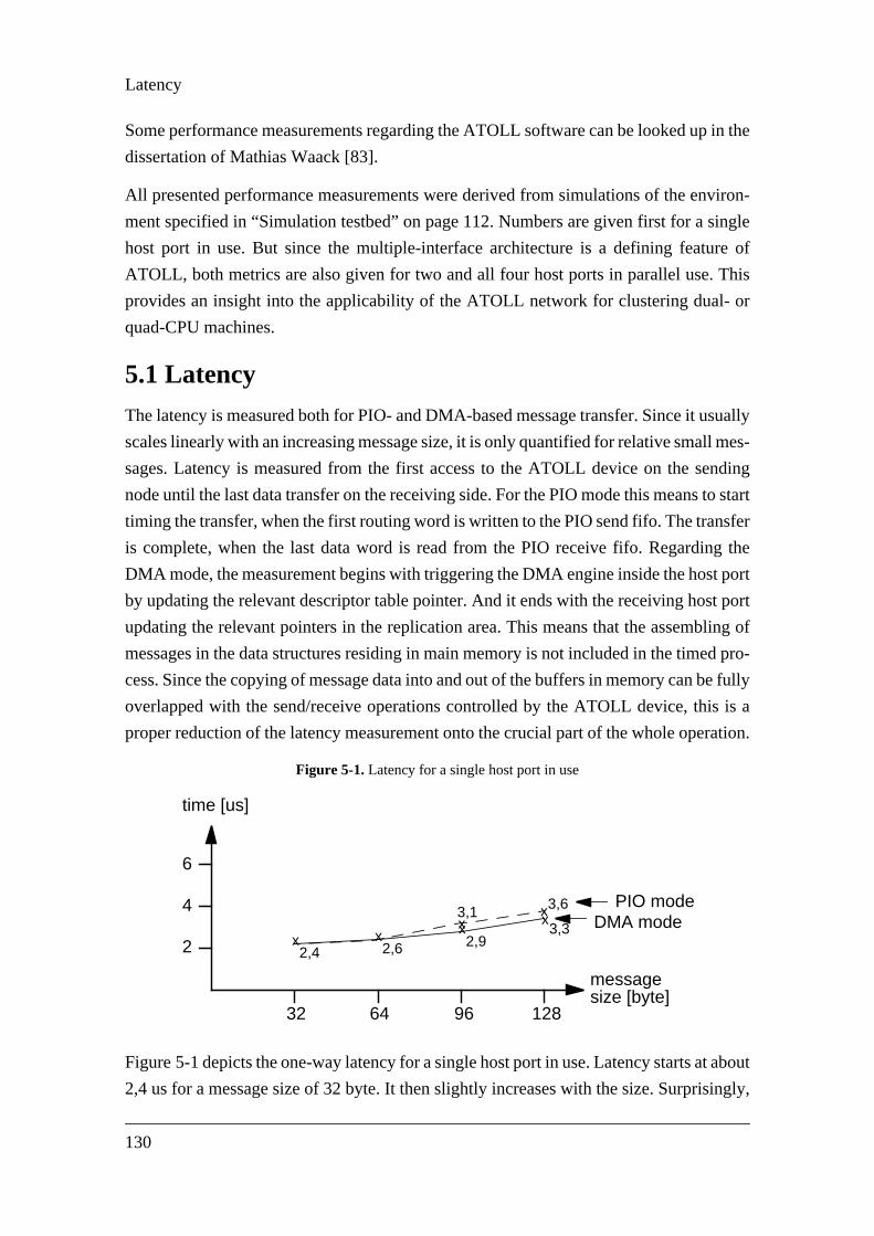
Latency
in the
viron-
ngle
e of
his
or
sually
mes-
nding
o start
sfer
the
port
port
ling of
d pro-
e fully
is a
ation.
about
ingly,
Some performance measurements regarding the ATOLL software can be looked up
dissertation of Mathias Waack [83].
All presented performance measurements were derived from simulations of the en
ment specified in “Simulation testbed” on page 112. Numbers are given first for a si
host port in use. But since the multiple-interface architecture is a defining featur
ATOLL, both metrics are also given for two and all four host ports in parallel use. T
provides an insight into the applicability of the ATOLL network for clustering dual-
quad-CPU machines.
5.1 Latency
The latency is measured both for PIO- and DMA-based message transfer. Since it u
scales linearly with an increasing message size, it is only quantified for relative small
sages. Latency is measured from the first access to the ATOLL device on the se
node until the last data transfer on the receiving side. For the PIO mode this means t
timing the transfer, when the first routing word is written to the PIO send fifo. The tran
is complete, when the last data word is read from the PIO receive fifo. Regarding
DMA mode, the measurement begins with triggering the DMA engine inside the host
by updating the relevant descriptor table pointer. And it ends with the receiving host
updating the relevant pointers in the replication area. This means that the assemb
messages in the data structures residing in main memory is not included in the time
cess. Since the copying of message data into and out of the buffers in memory can b
overlapped with the send/receive operations controlled by the ATOLL device, this
proper reduction of the latency measurement onto the crucial part of the whole oper
Figure 5-1.Latency for a single host port in use
Figure 5-1 depicts the one-way latency for a single host port in use. Latency starts at
2,4 us for a message size of 32 byte. It then slightly increases with the size. Surpris
messagesize [byte]
time [us]
2
4
6
32 64 96 128
x2,6
x2,9
x3,3
x2,4
DMA modex3,6 PIO mode
x3,1
130

Performance Evaluation
one
into
ome
ration
es,
d also
noti-
one
g side
for-
of a
ffect
tency
urther
host
roni-
up in
he idle
e bus
alue
the difference between PIO and DMA mode is almost negligible. At first glance,
could assume that the PIO mode would be slightly faster, since it directly writes data
the network on the sending side. Reading data from memory in DMA mode has s
more latency. But this is outweighed by the need to break up the PIO mode send ope
into 6 different PCI-X cycles, according to the PIO send address layout (3 fram
3 additional accesses for each last word of a frame). Some additional latency is adde
on the receiving side, since the complete reception of a message is not immediately
fied to the host CPU. The CPU polls the fifo fill level with a certain frequency, about
access each 0,3 us.
On the other hand, DMA mode needs only 3 PCI-X read transactions on the sendin
(descriptor, routing, header & data combined). Once data enters the ATOLL chip, it is
warded quite fast towards the network. E.g. it needs about 0,24 us for the first byte
message from the PCI-X bus to show up on the network link.
Figure 5-2.Latency for multiple host ports in use
Figure 5-2 shows that the number of active host ports in parallel has only a minor e
on message latency. Only DMA mode transfers were used. E.g. a15 % increase in la
for all four host ports in use is an acceptable value, compared to a single host port. F
investigation revealed that the multiple accesses to the PCI-X bus from different
ports were smoothly interleaved by the logic in the port interconnect and the synch
zation interface. During an active PCI-X transfer, several read requests can queue
the related data paths and can be started as soon as the current transfer is finished. T
time between back-to-back PCI-X transfers also depends on the performance of th
arbiter. The simulation used 6 PCI-X cycles to switch control of the bus, a similar v
should be found in real implementations.
messagesize [byte]
time [us]
2
4
6
32 64 96 128
x2,6
x2,9
x3,3
x2,4
1 HPx3,6
x3,2
x2,5 x2,8
2 HPx2,9 x
3,3x
3,8 4 HP
131
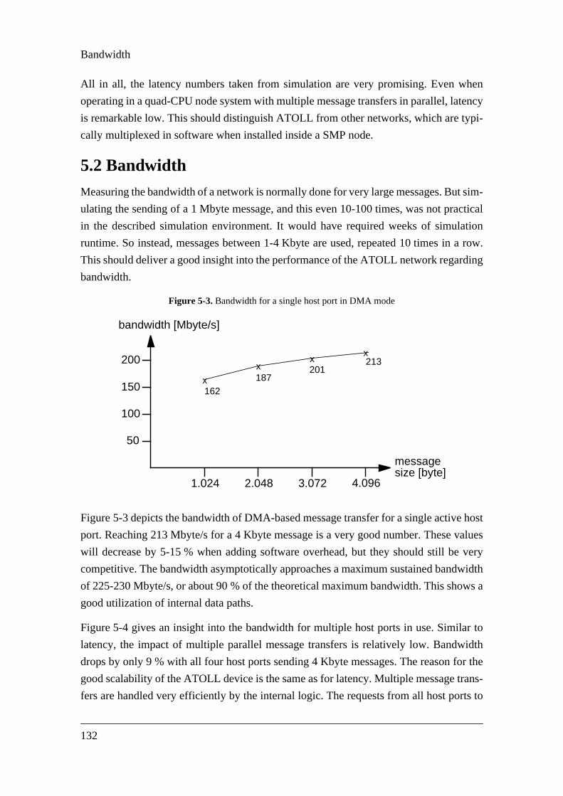
Bandwidth
hen
tency
pi-
sim-
ctical
tion
a row.
ing
host
alues
very
width
ws a
r to
idth
r the
ans-
ts to
All in all, the latency numbers taken from simulation are very promising. Even w
operating in a quad-CPU node system with multiple message transfers in parallel, la
is remarkable low. This should distinguish ATOLL from other networks, which are ty
cally multiplexed in software when installed inside a SMP node.
5.2 Bandwidth
Measuring the bandwidth of a network is normally done for very large messages. But
ulating the sending of a 1 Mbyte message, and this even 10-100 times, was not pra
in the described simulation environment. It would have required weeks of simula
runtime. So instead, messages between 1-4 Kbyte are used, repeated 10 times in
This should deliver a good insight into the performance of the ATOLL network regard
bandwidth.
Figure 5-3.Bandwidth for a single host port in DMA mode
Figure 5-3 depicts the bandwidth of DMA-based message transfer for a single active
port. Reaching 213 Mbyte/s for a 4 Kbyte message is a very good number. These v
will decrease by 5-15 % when adding software overhead, but they should still be
competitive. The bandwidth asymptotically approaches a maximum sustained band
of 225-230 Mbyte/s, or about 90 % of the theoretical maximum bandwidth. This sho
good utilization of internal data paths.
Figure 5-4 gives an insight into the bandwidth for multiple host ports in use. Simila
latency, the impact of multiple parallel message transfers is relatively low. Bandw
drops by only 9 % with all four host ports sending 4 Kbyte messages. The reason fo
good scalability of the ATOLL device is the same as for latency. Multiple message tr
fers are handled very efficiently by the internal logic. The requests from all host por
messagesize [byte]
bandwidth [Mbyte/s]
100
200
150
1.024 2.048 3.072 4.096
x162
50
x213x
x
187201
132

Performance Evaluation
ottle-
eep
byte-
ata
busy.
a-
sim-
hich
s.
read data from main memory are queued and served with minimum overhead. The b
neck is the PCI-X bus, but with its physical bandwidth of 1 Gbyte/s it is still able to k
all requesters busy. Regarding the internal conversion of a 64 bit data stream into a
wide link protocol in the network port, it is sufficient for a host port to deliver one d
word on each eighth cycle. This rate can be almost hold up, even for all host ports
Figure 5-4.Bandwidth for a multiple host ports in use
5.3 Resource Utilization
During the functional simulation of the ATOLL chip implementation, an efficient utiliz
tion of internal resources was a major goal, besides the validation of the logic. Early
ulations brought up some bottlenecks resulting from too few on-chip resources, w
then were resolved by enlarging fifo structures or performing similar enhancement
Figure 5-5.Network link utilization
messagesize [byte]
bandwidth [Mbyte/s]
100
200
150
1.024 2.048 3.072 4.096
x162
50
x213
xx187
201 1 HP
xx x x 2 HP
156
180192 202
xx x x
152176
187 195 4 HP
messagesize [byte]
link utilization [%]
50
100
75
1.024 2.048 3.072 4.096
x
88
25
65
8192
x
xxx
73
133

Resource Utilization
per-
the
es, as
cket
. total
ssage
ly
es.
and-
sage.
rout-
anage
ckets
t one
itive
cket
link
both
emory
ts the
byte.
rces
One major resource is the network link. Its efficient use is a crucial factor of overall
formance. So one driving force behind the definition of the link protocol was to keep
control overhead for sending packets as low as possible. The amount of control byt
defined in the link protocol for message framing, reverse flow control and pa
acknowledgment, is kept to the minimum possible.
Figure 5-5 shows the link utilization, given as rate between raw message data vs
bytes sent over the link for a message. Control overhead is quite high below a me
size of 1 Kbyte and makes up for about a third of link traffic. But utilization quick
exceeds 90 % and approaches a maximum value of nearly 95 % for large messag
Control bytes account for only a small portion of link overhead. Most of the wasted b
width is caused by small link packets, which normally appear at the head of a mes
The maximum size of 64 bytes is almost never used by link packets belonging to the
ing and header frames. Most of the messages sent via the ATOLL network should m
to get along with 1-3 data words (up to 24 data bytes). These consecutive link pa
introduce some idle time in the link ports, since only 2 packets can be in transit a
time. After both retransmission buffers have been filled, the link port waits for the pos
acknowledgment of the first packet. Only when the POSACK control byte for this pa
has been received, the buffer is freed and the next packet can be transmitted.
Figure 5-6.Idle time introduced by small link packets
Though only about 20 idle cycles are introduced when sending two back-to-back
packets with 16 byte payload, this short period of a blocked data path propagates in
directions along the link. E.g. it causes the delayed issue of a read request to main m
in the host port due to the lack of space in the main send data fifo. Figure 5-6 depic
situation mentioned, showing the idle time introduced by a late acknowledgment
But this situation is a rare event in the ATOLL architecture and the additional resou
1. link packet (16 byte)2. link packet (16 byte)3. link packet (64 byte)
link out
link in
t
idle time!
1. POSACK2. POSACK
134

Performance Evaluation
was
tem-
from
about
ntin-
, once
nd
y min-
that the
d-
more
, the
lot,
sed, a
ality,
rease
emon-
. The
LL
limit-
ser
of the
needed for more retransmission buffers far outweighed the gain. So the decision
made to get along with two buffers.
While message data travels through several top-level units in the ATOLL device, it is
porary stored in multiple data fifos spread all over the architecture. So a data path
the PCI-X bus towards the network can be seen as a very deep pipeline, with
40 register stages in total. The size of the fifos is tailored to provide a steady and co
uous data stream. It should be prevented that any of the main units runs out of data
a message transfer is started.
Figure 5-7.Fifo fill level variation
Figure 5-7 lists the variation of the fifo fill level along the data path for the DMA-se
mode. It is measured while sending a relatively large message. The numbers displa
imum and maximum fullness, once then message transfer has started. One can see
first two fifos still run empty during transmission. Only a fraction of the total PCI-X ban
width is used by a single path, so it is not necessary to keep these fifos filled. The
one gets towards the network, the higher is the average fill level of fifos. Once started
last 3 fifos never run out of data during a message transfer. The fill level still varies a
mainly just after the operation started. But once a few data words have been proces
contiguous data stream keeps all units busy.
All performance measurements were done assuming no network contention. In re
this assumption is of course too optimistic. So performance numbers will also dec
due to network congestion. But the performance values presented in this chapter d
strate that the ATOLL architecture is capable of maximizing most internal resources
network is no more the communication bottleneck in a cluster equipped with the ATO
network. Instead, the interface to the host system, in this case the PCI-X bus, is the
ing factor. One can overcome this limitation only by locating the network interface clo
to the CPU, e.g. on the system bus. But as mentioned earlier, this restricts the use
NI to a single microprocessor architecture.
synch.interfacerequester
portinterconnectMasterRead.
host portDMA-send
networkportsend
link portsendunit
fill levelvariation
0-48 % 0-75 % 14-93 % 24-88 % 32-92 %
135

Resource Utilization
136

Conclusions
ers in
ass-
rs and
rt to
ar for
orks
for-
order
/per-
new
y.
mput-
-CPU
cost
e. And
es an
p for-
ved
of a
nly
-wide
dif-
6Conclusions
Clusters are emerging as a competitive alternative to Vector or MPP supercomput
the field of High Performance Computing. The excellent price/performance ratio of m
market PC technology makes it very attractive to assemble lots of desktop compute
tie them together with a high performance network. These Beowulf computers sta
show up in rankings like the Top500 supercomputer list, and are even more popul
assembling small- to medium-sized clusters of 32-256 nodes.
The key component is a fast network. A new class of so-called System Area Netw
emerged, since the traditional LAN/WAN technology was quickly identified as a per
mance bottleneck. SANs like Myrinet, SCI and QsNet offer message latencies in the
of 5-15 us and sustained bandwidths in the range of 100-300 Mbyte/s. But the price
formance ratio of most networks is still too high to gain a broader acceptance of these
SANs. So the majority of clusters is still equipped with standard Ethernet technolog
Recent trends in PC technology pose new problems to SANs. E.g. SMP desktop co
ers are becoming available at a price advantage, compared to multiple single
machines. New clusters are often assembled with dual-CPU nodes. This offers a
advantage, together with less requirements for area, administration and power usag
the next generation of microprocessor technology will even make 4-8 CPU SMP nod
attractive node option, mostly based on better SMP support by CPUs.
To sum up, current SAN technology has helped Cluster Computing to make a big ste
ward, but there is still plenty of room for improvements in performance and cost.
6.1 The ATOLL SAN
This dissertation introduces a novel SAN version of the ATOLL architecture, deri
from a first MPP version of the architecture. It integrates all necessary components
network into one single chip, including the switch. ATOLL provides support for not o
one, but four network interfaces by an aggressive replication of resources. Four byte
link interfaces running at 250 MHz offer the possibility to directly connect nodes in
ferent topologies, without the need for any external switching hardware.
137

Future work
and
mall
dth for
tifica-
tatus
one in
evel.
mis-
by a
PCI-X
idth
the
titive
sup-
lus-
.
tion
xity
phis-
ayout
t the
by a
ntest
by
s like
ill
3GIO
ATOLL offers a sophisticated mechanism to dynamically choose between PIO-
DMA-based message transfer. This supports extremely low start-up latency for s
messages through a Programmed I/O interface, as well as high sustained bandwi
large messages by autonomous DMA engines inside each host port. An efficient no
tion mechanism avoids the use of costly interrupts by a cache-coherent polling of s
registers in main memory. The consecutive sending/receiving of messages can be d
an overlapping fashion, keeping the utilization of internal resources at a very high l
An error detection and correction protocol avoids end-to-end control of data trans
sions. Bit errors introduced by environmental effects are discovered and solved
packet retransmission mechanism on each link. On the host side, a state-of-the-art
interface offers up to 1 Gbyte/s of I/O bandwidth. This is needed to serve the bandw
requirements of the ATOLL core, which has a bisection bandwidth of 2 Gbyte/s on
network side.
Early performance evaluations promise extremely low latency and a very compe
sustained bandwidth of ATOLL. Multiple data transfers via all four host ports can be
ported with a negligible performance impact. This will be an outstanding feature of a c
ter composed out of SMP nodes, which are equipped with the ATOLL network card
Besides redesigning the architecture of ATOLL towards a SAN, this disserta
describes also the implementation of the ATOLL ASIC. Its sheer size and comple
posed a lot of problems, which were solved by a well-planned design flow and a so
ticated design methodology. Despite not quite reaching the timing goal, a transistor l
of the chip was shipped to prototype production in February 2002. It is expected tha
real chips can be operated at about 90 % of the targeted clock frequency.
The ATOLL ASIC is one of the most complex and fastest chips ever implemented
European university. Recently, the design has won the third place in the design co
organized at the Design, Automation & Test in Europe (DATE) conference1, the premier
European event for electronic design.
6.2 Future work
The future development of a second generation of ATOLL will be greatly influenced
technology trends in the whole computer industry. Upcoming interconnect standard
InfiniBand target the server-to-server connection. But it is still questionable, if it w
really take over the whole range of I/O as predicted. Other emerging standards like
1. www.date-conference.com
138

Conclusions
r for
ices
own
varia-
sion
nolo-
eci-
sical
ced
ode
to the
rna-
ode.
all
e by
the
same
ded
ology,
This
usage
. The
ible,
IC
than
larger
from Intel are still in the specification phase, but might become a serious contende
InfiniBand in the area of low-level I/O connectivity, as needed for graphics, I/O dev
(keyboard, mouse, modem), etc. InfiniBand might be restricted to the fields now kn
as Storage Area Networks, replacing such technologies as Fiber Channel and all
tions of SCSI. But how both technologies coexist is still part of an ongoing discus
[84]. On the other hand, recent optimizations have been specified for existing tech
gies like PCI-X. The next generation of PCI-X, as specified in the upcoming v2.0 sp
fication, will support dual- or quad-pumped data busses, raising the maximal phy
bandwidth to 4 Gbyte/s.
Of course, the definition of the next generation architecture will be also greatly influen
by the experiences users gain with the first generation of ATOLL. E.g. the PIO m
takes up significant resources inside the chip. If the performance gain, compared
DMA mode, is not large enough to justify the additional resources, it might be an alte
tive to drop it and use the free resources for a better implementation of the DMA m
Mainly there are two options for the development of the next version of ATOLL. A sm
and easier to manage option is a so-called technology shrink. It is normally don
making only minor modifications to the overall architecture, but implementing it in
newest technology. So within 1-2 years, one could again implement almost the
architecture by the following steps:
• using a 0.10 um CMOS technology, targeting a core frequency of 500-700 MHz
• going from parallel copper cables to serial fiber links. The reduced pin count nee
would also offer the possibility to increase the number of link interfaces to 6-8
• moving from a PCI-X v1.0 bus interface to a PCI-X v2.0 interface offering up to
4 Gbyte/s
• enlarging internal RAM/fifo structures to provide more buffer space
These enhancements would help to keep up with the progress in desktop techn
resulting in a network with three or four times the performance of the current version.
is a possible alternative if no major design flaws are detected during the widespread
of the first version.
A more challenging approach would be a major redesign of the whole architecture
current one is efficient but not very flexible. Adding new features is almost imposs
due to the fixed implementation of all control logic in hardware. The current trend in
design is moving towards so-called Systems-on-a-Chip (SoC) designs. Rather
designing all necessary logic from scratch, one assembles pre-build IP blocks into a
139

Future work
ed in
PC,
logy
nt of
age of
mber
ould
r lay-
and
ork,
. But
ys
ld be
ntro-
s the
et in
system. These blocks can be bus interfaces, like the PCI-X interface already us
ATOLL. But a lot of microprocessor cores are also available, e.g. MIPS, ARM, Power
etc. So one could take advantage of the millions of transistors modern IC techno
offers by a mixture of soft- and hardmacros, which are glued together by some amou
self-implemented logic. Recent market surveys have shown that the current percent
chip area used by IP cells is about 20-30 %. Some reports [85] predict that this nu
increases to 80-90 % within the next 5 years. This way, the implementation effort c
be kept manageable, since most of the logic comes as completely verified transisto
out. More concentration could be devoted to the definition of the overall architecture
its fine tuning for highest performance.
The architecture would head towards the ones of Myrinet, QsNet or the IBM SP netw
which all have a programmable microprocessor as the key component of the NIC
ATOLL would offer the whole system combined on a single chip. And with toda
advanced technology, even multiple controllers could be implemented. This cou
used to split up the work into a host and a network side, avoiding any bottlenecks i
duced by off-loading too much work onto a single controller.
Both options have their pros and cons. But it shows that the ATOLL architecture ha
potential to compete with the most advanced commercial solutions in the SAN mark
the future.
140

y col-
tech-
ally
nt of
le-
set-
nted
iew.
os-
Acknowledgments
This thesis would not have been possible without the help and contributions by man
leagues. My advisor Professor Dr. Ulrich Brüning was always available to discuss
nical issues and provided a working environment, which made it possible to fin
complete one of the largest non-commercial chip projects.
The whole team of the Chair of Computer Architecture contributed to the developme
the ATOLL network. My colleague Patrick Schulz took over crucial parts of the imp
mentation like the insertion of test structures and provided significant support while
ting up the complex functional testbed. And my colleague Mathias Waack impleme
all the software necessary to make use of the ATOLL network from a user’s point of v
I would like to thank all those individuals for their contributions, which gave me the p
sibility to complete my own work.
i

ii

res
TR,
el
ek,
ial
ya A.
tific
e on
ing
lti-
R-
re."
go-
lec-
n-
Bibliography
[1] Rajkumar Buyya (editor). "High Performance Cluster Computing: Architectu
and Systems, Volume 1." Prentice Hall PTR, 1999.
[2] Gregory F. Pfister. "In Search of Clusters, Second Edition." Prentice Hall P
January 1998.
[3] William Gropp, Ewing Lusk, Anthony Skjellum. "Using MPI: Portable Parall
Programming with the Message-Passing Interface." MIT Press, 1994.
[4] Al Geist, Adam Beguelin, Jack Dongarra, Weicheng Jiang, Robert Manch
Vaidy Sunderam. "PVM: Parallel Virtual Machine - A Users’ Guide and Tutor
for Networked Parallel Computing." MIT Press, 1994.
[5] Thomas Sterling, Daniel Savarese, Donald J. Becker, John E. Dorband, Uda
Ranawake, Charles V. Packer. "BEOWULF: A Parallel Workstation For Scien
Computation." CRC Press, Proceedings of the 24th International Conferenc
Parallel Processing, Volume I, pages 11-14, Boca Raton, FL, August 1995.
[6] The Top500 Supercomputer List, www.top500.org
[7] Ian Foster, Carl Kesselman (editors). "The Grid: Blueprint for a New Comput
Infrastructure." Morgan Kaufmann Publishers, July 1998.
[8] Jakov N. Seizovic. "The Architecture and Programming of a Fine-Grain Mu
computer." California Institute of Technology (Caltech), Technical Report CS-T
93-18, 1993.
[9] Duncan Roweth. "Industrial Presentation: The Meiko CS-2 System Architectu
ACM Press, Proceedings of the 5th Annual ACM Symposium on Parallel Al
rithms and Architectures, page 213, June 1993.
[10] Gordon E. Moore. "Cramming more Components onto Integrated Circuits." E
tronics, Volume 38, Number 8, April 1965.
[11] Donald E. Thomas, Philip R. Moorby. "The Verilog Hardware Description La
guage, Third Edition." Kluwer Academic Publishers, 1996.
iii

er
the
er-
DL
h to
the
itos,
es,
lid-
ical
ro-
ion
with
nal
om-
or-
cy:
7.
et-
onal
[12] Ben Cohen. "VHDL Coding Styles and Methodologies, 2nd Edition." Kluw
Academic Publishers, 1999.
[13] J. Bhasker, Sanjiv Narayan. "RTL Modeling Using SystemC." Proceedings of
International HDL Conference, San Jose, CA, March 2002.
[14] Peter L. Flake, Simon J. Davidmann, David J. Kelf. "SUPERLOG: Evolving V
ilog and C for System-on-Chip Design." Proceedings of the International H
Conference, San Jose, CA, March 2000.
[15] Nagaraj, Frank Cano, Haldun Haznedar, Duane Young. "A Practical Approac
Static Signal Electromigration Analysis." ACM/IEEE Press, Proceedings of
1998 Conference on Design Automation (DAC), pages 572-577, Los Alam
CA, June 1998.
[16] Patrick P. Gelsinger. "Microprocessors for the New Millennium -Challeng
Opportunities and New Frontiers." Proceedings of the IEEE International So
State Circuits Conference (ISSCC), San Francisco, CA, February 2001.
[17] Sun Microsystems, Inc. "Sun Compute Farms for Electronic Design." Techn
White Paper, 2000.
[18] Raoul A. Bhoedjang, Tim Rühl, Henri E. Bal. "User-Level Network Interface P
tocols." IEEE Computer, Vol. 31, No. 11, pages 53-60, November 1998.
[19] Matt Welsh, Anindya Basu, Thorsten von Eicken. "Low-Latency Communicat
over Fast Ethernet." Proceedings EUROPAR-96, August 1996.
[20] Giuseppe Ciaccio. "Optimal Communication Performance on Fast Ethernet
GAMMA." Springer, Proceedings of the International Workshop on Perso
Computers based Networks Of Workstations (PC-NOW), Lecture Notes in C
puter Science (LNCS) 1388, Orlando, Florida, March 1998.
[21] Scott Pakin, Vijay Karamcheti, Andrew A. Chien. "Fast Messages: Efficient, P
table Communication for Workstation Clusters and MPPs." IEEE Concurren
Parallel Distributed & Mobile Computing, Vol. 5, No. 2, pages 60-73, April 199
[22] Yueming Hu. "A Simulation Research on Multiprocessor Interconnection N
works with Wormhole Routing." IEEE-CS Press, Proceedings of the Internati
iv
hina,
nt,
f the
A),
:
er-
ry
le
on
ges
12th
os-
ing
"A
ngs
isco,
ca-
nd
for
Conference on Advances in Parallel and Distributed Computing, Shanghai, C
March 1997.
[23] B. H. Lim, P. Heidelberger, P. Pattnaik, M. Snir. "Message Proxies for Efficie
Protected Communication on SMP Clusters." IEEE-CS Press, Proceedings o
International Symposium on High Performance Computer Architecture (HPC
pages 116-127, February 1997.
[24] Wolfgang K. Giloi, Ulrich Brüning, Wolfgang Schröder-Preikschat. "MANNA
Prototype of a Distributed Memory Architecture with Maximized Sustained P
formance." Proceedings Euromicro PDP Workshop, 1996.
[25] Marco Fillo, Richard B. Gillett. "Architecture and Implementation of Memo
Channel 2." Digital Technical Journal, Vol. 9/1, 1997.
[26] James Laudon, Daniel Lenoski. "The SGI Origin: A ccNUMA Highly Scalab
Server." ACM Press, Proceedings of the 24th Annual International Symposium
Computer Architecture (ISCA), Computer Architecture News, Vol. 25/2, pa
241-251, June 1997.
[27] Colin Whitby-Strevens. "The Transputer." IEEE Press, Proceedings of the
International Symposium on Computer Architecture (ISCA), pages 292-300, B
ton, MA, June 1985.
[28] Thomas Gross, David R. O’Hallaron. "iWarp: Anatomy of a Parallel Comput
System." MIT Press, 1998.
[29] Robert O. Mueller, A. Jain, W. Anderson, T. Benninghoff, D. Bertucci, et. al.
1.2GHz Alpha Microprocessor with 44.8GB/s Chip Pin Bandwidth." Proceedi
of the IEEE International Solid-State Circuits Conference (ISSCC), San Franc
CA, February 2001
[30] PCI Special Interest Group. "PCI-X Addendum to the PCI Local Bus Specifi
tion." PCI-SIG, Revision 1.0, September 1999.
[31] Ajay V. Bhatt. "Creating a Third Generation I/O Interconnect." Technology a
Research Labs, Intel Corp., Whitepaper, 2001.
[32] Isaac D. Scherson, Abdou S. Youssef (editors). "Interconnection Networks
High-Performance Parallel Computers." IEEE-CS Press, 1994.
v

for
ges
An
ulti-
10,
lti-
l. C-
rol
12th
ions,
n-
rk-
Feb-
rent
rs."
er,
ces
CM
uter
es
[33] Andrew A. Chien, Mark D. Hill, Shubhendu S. Mukherjee. "Design Challenges
High-Performance Network Interfaces." IEEE Computer, Vol. 31, No. 11, pa
42-45, November 1998.
[34] Jose Duato, Sudhakar Yalamanchili, Lionel Ni. "Interconnection Networks:
Engineering Approach." IEEE-CS Press, 1997.
[35] Prasant Mohapatra. "Wormhole routing techniques for directly connected m
computer systems." ACM Computing Surveys, Vol. 30, No. 3, pages 374-4
September 1998.
[36] William J. Dally and Charles L. Seitz. "Deadlock-Free Message Routing in Mu
processor Interconnection Networks." IEEE Transactions on Computers, Vo
36, No. 5, pages 547-553, 1987.
[37] Allan R. Osborn, Douglas W. Browning. "A Comparative Study of Flow Cont
Methods in High-Speed Networks." IEEE-CS Press, Proceedings of the
Annual International Phoenix Conference on Computers and Communicat
pages 353-359, Tempe, AR, March 1993.
[38] David C. DiNucci. "Programming Parallel Processors: Alliant FX/8." Addiso
Wesley, pages 27-42, 1988.
[39] Jeff Larson. "The HAL Interconnect PCI Card." Springer, 2nd International Wo
shop CANPC, Lecture Notes in Computer Science, Vol. 1362, Las Vegas, NV,
ruary 1998.
[40] Hermann Hellwagner, Alexander Reinefeld (editors). "SCI: Scalable Cohe
Interface, Architecture and Software for High-Performance Compute Cluste
Springer, Lecture Notes in Computer Science, Vol. 1734, 1999.
[41] Data General Corp. "AViiON AV 20000 Server Technical Overview." White Pap
1997.
[42] G. Abandah, E. Davidson. "Effects of Architectural and Technological Advan
on the HP/Convex Exemplar’s Memory and Conmmunication Performance." A
Press, Proceedings of the 25th Annual International Symposium on Comp
Architecture (ISCA), ACM Computer Architecture News, Vol. 26, No. 3, pag
318-329, June 1998.
vi

rm
llel
, NV,
h-
SCI
PC
a
hni-
c-
vic,
er
e
CM/
ber
on
ss,
San
[43] David X. Wang. "New Scalable Parallel Computer Architecture - Non-Unifo
Memory Access (NUMA-Q)." IEEE Press, International Conference on Para
and Distributed Processing Techniques and Applications (PDPTA), Las Vegas
June 1997.
[44] Ch. Kurmann, Thomas Stricker. "A Comparison of two Gigabit SAN/LAN tec
nologies: Scalable Coherent Interface versus Myrinet." Proceedings of the
Europe Conference (EMMSEC), Bordeaux, France, September 1998.
[45] David Garcia, William Watson. "ServerNet II." Springer, Proceedings CAN
Workshop, Lecture Notes in Computer Science, Vol. 1417, 1998.
[46] Alan Heirich, David Garcia, Michael Knowles, Robert Horst. "ServerNet-II:
Reliable Interconnect for Scalable High Performance Cluster Computing." Tec
cal Report, Compaq Computer Corporation, September 1998.
[47] Compaq Computer Corp., Intel Corp., Microsoft Corp. "Virtual Interface Archite
ture Specification." Version 1.0, December 1997.
[48] N. J. Boden, D. Cohen, R. E. Felderman, A. E. Kulawik, C. L. Seitz, J. N. Seizo
Wen-King K. Su. "Myrinet - A Gigabit-per-Second Local-Area-Network." IEEE
Micro, Vol. 15, No. 1, pages 29-36, February 1995.
[49] Myricom, Inc. www.myri.com.
[50] Myricom, Inc. "Guide to Myrinet-2000 Switches and Switch Networks." Us
Guide, August 2001.
[51] Steven S. Lumetta, Alan Mainwaring, David E. Culler. "Multi-protocol Activ
Messages on a Cluster of SMPs." ACM/IEEE-CS Press, Proceedings of the A
IEEE International Conference on Supercomputing, San Jose, CA, Novem
1997.
[52] Scott Pakin, Mario Lauria, Andrew Chien. "High Performance Messaging
Workstations: Illinois Fast Messages (FM) for Myrinet." ACM/IEEE-CS Pre
Proceedings of the ACM/IEEE International Conference on Supercomputing,
Diego, CA, November 1995.
vii

er-
ce,
ion
s in
a-
ster
5th
erg.
ro,
per,
er,
hip
M/
ber
&
r,
on
ce on
[53] Loic Prylli, Bernard Tourancheau. "BIP: A New Protocol Designed for High P
formance Networking on Myrinet." Springer, Lecture Notes in Computer Scien
Vol. 1388, 1998.
[54] Joachim M. Blum, Thomas M. Warschko, Walter F. Tichy. "PULC: ParaStat
User-Level Communication. Design and Overview." Springer, Lecture Note
Computer Science, Vol. 1388, 1998.
[55] Myricom, Inc. "The GM Message Passing System." User Guide, 2000.
[56] Yutaka Ishikawa, Hiroshi Tezuka, Atsuhi Hori, Shinji Sumimoto, Toshiyuki Tak
hashi, Francis O’Carroll, Hiroshi Harada. "RWC PC Cluster II and SCore Clu
System Software - High Performance Linux Cluster." Proceedings of the
Annual Linux Expo, pages 55-62, 1999.
[57] Fabrizio Petrini, Wu-chun Feng, Adolfy Hoisie, Salvador Coll, Eitan Frachtenb
"The Quadrics Network: High-Performance Clustering Technology." IEEE Mic
No. 1, pages 46-57, January 2002.
[58] Compaq Computer Corp. "Compaq Alpha SC Announcement." Whitepa
November 1999.
[59] IBM. "RS/6000 SP: SP Switch2 Technology and Architecture." Whitepap
March 2001.
[60] Craig B. Stunkel, Jay Herring, Bulent Abali, Rajeev Sivaram. "A New Switch C
for IBM RS/6000 SP Systems." ACM/IEEE-CS Press, Proceedings of the AC
IEEE International Conference on Supercomputing, Portland, OR, Novem
1999.
[61] InfiniBand Trade Association. "InfiniBand Architecture Specification." Vol.1, 2
3, Rev 1.0, October 2000.
[62] IBM. "InfiniBand: Satisfying the Hunger for Network Bandwidth." Whitepape
June 2001.
[63] Ulrich Brüning, Lambert Schaelicke. "Atoll: A High-Performance Communicati
Device for Parallel Systems." IEEE-CS Press, Proceedings of the Conferen
Advances in Parallel and Distributed Computing, pages 228-234, 1997.
viii

ec-
Sixth
ges
us
d-
N-
lz,
et-
ies
ey,
K
di-
of
68,
el
-A-
[64] Peter M. Behr, Samuel Pletner, A. C. Sodan. "PowerMANNA: A Parallel Archit
ture Based on the PowerPC MPC620." IEEE-CS Press, Proceedings of the
International Symposium on High-Performance Computer Architecture, pa
277-286, Toulouse, France, January 2000.
[65] Synopsys, Inc. "DesignWare DW_pcix MacroCell Databook." October 2001.
[66] PCI Special Interest Group (PCISIG). "PCI-X Addendum to the PCI Local B
Specification." Revision 1.0, September 1999.
[67] Ulrich Brüning, Jörg Kluge, Lars Rzymianowicz, Patrick Schulz. "ATOLL Har
ware Reference Manual." Internal Databook, 2002.
[68] Berthold Lehmann. "Implementation of an efficient hostport for the ATOLL SA
Adapter." Diploma Thesis, Institute of Computer Engineering, University of
Mannheim, March 1999.
[69] Jörg Kluge, Ulrich Brüning, Markus Fischer, Lars Rzymianowicz, Patrick Schu
Mathias Waack. "The ATOLL approach for a fast and reliable System Area N
work." Third Intl. Workshop on Advanced Parallel Processing Technolog
(APPT’99) conference, Changsha, P.R. China, October 1999.
[70] Michael J. S. Smith. "Application-Specific Integrated Circuits." Addison-Wesl
VLSI Systems Series, 1997.
[71] Pran Kurup, Taher Abbasi, Ricky Bedi. "It’s the Methodology, Stupid!" Byte
Designs, Inc., 1998.
[72] Lars Rzymianowicz. "FSMDesigner: Combining a Powerful Graphical FSM E
tor and Efficient HDL Code Generation with Synthesis in Mind." Proceedings
the 8th International HDL Conference and Exhibition (HDLCON), pages 63-
Santa Clara, CA, April 1999.
[73] Tim Leuchter, Lars Rzymianowicz. "Guidelines for writing efficient RTL-lev
Verilog HDL code." University of Mannheim,
http://mufasa.informatik.uni-mannheim.de/lsra/persons/lars/verilog_guide
[74] Michael Keating, Pierre Bricaud. "Reuse Methodology Manual for System-On
Chip Designs, 2nd Edition." Kluwer Academic Publishers, June 1999.
ix

lti-
ose,
on."
psys
User
of
eet-
e
n-
st: A
the
-
ica-
ng,
ata
tom
.
[75] Clifford E. Cummings. "Synthesis and Scripting Techniques for Designing Mu
Asynchronous Clock Designs." Synopsys User Group Meeting (SNUG), San J
CA, March 2001.
[76] Peet James. "Shotgun Verification: The Homer Simpson Guide to Verificati
Synopsys User Group Meeting (SNUG), Boston, MA, September 2001.
[77] Synopsys, Inc. "Automated Chip Synthesis User Guide, v2001-08." Syno
Online Documentation (SOLD), August 2001.
[78] Steve Golson. "A Comparison of Hierarchical Compile Strategies." Synopsys
Group Meeting (SNUG), San Jose, CA, March 2001.
[79] Rick Furtner. "High Fanout without High Stress: Synthesis and Optimization
High-Fanout Nets using Design Compiler 2000.11." Synopsys User Group M
ing (SNUG), Boston, MA, September 2001.
[80] Patrick Schulz. "Design for Test (DfT) and Testability of a Multi-Million Gat
ASIC." Diploma Thesis, Institute of Computer Engineering, University of Ma
nheim, November 2000.
[81] Harry Bleeker, Peter van den Eijnden, Frans de Jong. "Boundary-Scan Te
Practical Approach." Kluwer Academic Publishers, 1993.
[82] Erich Krause. "Integration, Test and Validation of a PCI IP Macrocell into
Multi-Million Gate ATOLL ASIC." Diploma Thesis, Institute of Computer Engi
neering, University of Mannheim, April 2001.
[83] Mathias Waack. "Concepts, Design and Implementation of efficient Commun
tion Software for System Area Networks." Institute of Computer Engineeri
University of Mannheim, June 2002.
[84] IBM. "InfiniBand and Arapahoe/3GIO: Complementary Technologies for the D
Center." Whitepaper, February 2002.
[85] International Business Strategies, Inc. "Analysis of SoC Design Costs: A Cus
Study for Synopsys Professional Services." Technical Report, February 2002
x