determining the internal quantum efficiency of pbse ...lawm/determining the internal...determining...
TRANSCRIPT

Determining the Internal QuantumEfficiency of PbSe Nanocrystal SolarCells with the Aid of an Optical ModelMatt Law,*,† Matthew C. Beard,† Sukgeun Choi, Joseph M. Luther,Mark C. Hanna, and Arthur J. Nozik
National Renewable Energy Laboratory, Golden, Colorado 80401
Received August 2, 2008; Revised Manuscript Received September 5, 2008
ABSTRACT
We determine the internal quantum efficiency (IQE) of the active layer of PbSe nanocrystal (NC) back-contact Schottky solar cells by combiningexternal quantum efficiency (EQE) and total reflectance measurements with an optical model of the device stack. The model is parametrizedwith the complex index of refraction of each layer in the stack as calculated from ellipsometry data. Good agreement between the experimentaland modeled reflectance spectra permits a quantitative estimate of the fraction of incident light absorbed by the NC films at each wavelength,thereby yielding well-constrained QE spectra for photons absorbed only by the NCs. Using a series of devices fabricated from 5.1 ( 0.4 nmdiameter PbSe NCs, we show that thin NC cells achieve an EQE and an active layer IQE as high as 60 ( 5% and 80 ( 7%, respectively, whilethe QE of devices with NC layers thicker than about 150 nm falls, particularly in the blue, because of progressively greater light absorptionin the field-free region of the films and enhanced recombination overall. Our results demonstrate that interference effects must be taken intoaccount in order to calculate accurate optical generation profiles and IQE spectra for these thin film solar cells. The mixed modeling/experimentalapproach described here is a rigorous and powerful way to determine if multiple exciton generation (MEG) photocurrent is collected bydevices with EQE < 100%. On the basis of the magnitudes and shapes of the IQE spectra, we conclude that the 1,2-ethanedithiol treated NCdevices studied here do not produce appreciable MEG photocurrent.
Light absorption in a thin film solar cell can be greatlyaffected by optical interference if the device is optically thinand has a highly reflective back electrode. When theseconditions are met, the buildup of an optical mode structurewill change the absorption spectra of the active materialsrelative to their spectra when free of the optical cavity formedby the device stack. Exponential, Beer’s Law type absorption/generation profiles cannot then be assumed, and accuratevalues of the internal quantum efficiency (IQE) of the activelayers of the device can be obtained only by determiningtheir absorption spectra as they exist within the devicestructure.
The IQE of a solar cell is normally calculated from theratio of its external quantum efficiency (EQE) and spectralabsorptance as IQE(λ) ) EQE(λ)/[1 - F(λ) - τ(λ)], whereF(λ) is the spectral reflectance and the device transmittanceτ(λ) is usually zero. However, this approach can give anunderestimated and misleading IQE spectrum if incident lightis absorbed by the electrodes and other nonactive layers ofthe device in addition to the active semiconductor layer(s).
We show here that the quantum efficiency of photonsabsorbed only within the active layer of a PbSe nanocrystalback-contact Schottky solar cell1 can be determined bycombining reflectance measurements with an optical modelcapable of discerning the fraction of light absorbed in eachof the layers within the device stack. An accurate determi-nation of the IQE is essential for ascertaining whethermultiple exciton generation (MEG) photocurrent is generatedby these devices. An IQE substantially greater than 100%for sufficiently high-energy photons (hν g 3Eg) wouldindicate that MEG is occurring.
Experimental Section. Materials. Lead oxide (PbO,99.999%), selenium (99.99%), oleic acid (OA, tech. grade,90%), diphenylphosphine (DPP, 98%), 1-octadecene (ODE,90%), and anhydrous solvents were purchased from Aldrichand used as received. Trioctylphosphine (TOP, tech. grade,>90%) and 1,2-ethanedithiol (EDT, >98%) were acquiredfrom Fluka. Calcium pieces (99.99%) and aluminum shot(99.999%) were purchased from Cerac and Aldrich, respec-tively.
NC Synthesis. A single 0.8 g sample of NCs having afirst exciton transition at 1686 nm (0.735 eV) was used forthis study. The NCs were synthesized and purified usingstandard airfree techniques. A solution of 3.01 g PbO (13.5mmol), 10.61 g oleic acid (37.6 mmol), and 0.514 g DPP
* To whom correspondence should be addressed. Present address:Department of Chemistry, University of California, Irvine. E-mail:[email protected].
† These authors contributed equally to this work.
NANOLETTERS
2008Vol. 8, No. 11
3904-3910
10.1021/nl802353x CCC: $40.75 2008 American Chemical SocietyPublished on Web 09/30/2008
(2.76 mmol) in 70.05 g ODE was degassed and heated to180 °C in a reaction flask for one hour. Thirty-five millilitersof a 1 M solution of TOP-Se was then rapidly injected intothis hot solution. The NCs were grown at 145 °C for 90 s,and the reaction was rapidly quenched with a water bathand 50 mL of anhydrous hexane. The NCs were purified byprecipitation twice in hexane/acetone and once in hexane/ethanol and stored in a glovebox as a powder.
DeWice Fabrication. PbSe NC films were deposited ontoprecleaned, patterned ITO-coated glass substrates (12 Ω/sq.,Colorado Concept Coatings) using a layer-by-layer dipcoating procedure modified from our previous reports1,2 toyield uniform, optically perfect films across larger areas(square inches). Rather than dipping the films by hand, amechanical dip coater mounted inside of a glovebox (DC-Multi-4, Nima Technology) repetitively dipped the substratesinto a 4 mg mL-1 solution of NCs in dry hexane and then a0.002 M solution of 1,2-ethanedithiol (EDT) in dry aceto-nitrile. Glassy, crack-free, and mildly conductive (σ ) 5 ×10⁻⁵ S cm-1 in the dark) NC films are produced in this way.Film thickness is linear with the number of dipping cyclesfor a fixed dipping speed (Supporting Information, FigureS1). We fabricated NC films with thicknesses in the 30-450nm range. Unwanted areas of each film were removed witha razor blade. Top contacts (15 nm Ca/60 nm Al) were thendeposited through a shadow mask in a glovebox thermalevaporator (2 × 10⁻⁸ Torr base pressure, Angstrom Engi-neering) at a rate of 0.2 Å s-1 for the Ca and 1.0 Å s-1 forthe Al. This procedure yields six devices per substrate, eachwith an active area of 0.105 cm2.
Characterization, Modeling, and DeWice Testing. Thecomplex refractive index n(λ) ) n(λ) + ik(λ) of the glass,ITO, NC film, and Al layers were determined from 200 to1700 nm by rotating compensator-type, variable-angle spec-troscopic ellipsometry (J. A. Woollam Co. M2000) at roomtemperature. The incidence angle was varied from 65 to 75°and the spectral resolution was 1.6 nm. Transmittancemeasurements were acquired in a normal-incidence config-uration. Samples were prepared on undoped, polished siliconsubstrates or glass microscope slides and measured under acontinuous flow of dry nitrogen seconds after removing themfrom airfree transfer tubes. The measured data were analyzedusing the multiphase model (substrate/interface roughness/film/surface roughness/ambient). A set of Gaussian andLorentzian oscillators was employed in the model toreproduce the optical spectra of the films. The thickness andsurface roughness of each sample were also estimated byscanning electron microscopy (SEM) (JEOL JSM-700F) andatomic force microscopy (AFM) (Veeco Dimension 3100in tapping mode). The film thicknesses and the surfaceroughnesses determined by ellipsometric measurements werein good agreement with the results from SEM and AFManalyses. We found the optical functions of the NC films tobe independent of film thickness. The resulting n(λ) and k(λ)of each material were then used to parametrize the opticalmodel of the device.
For reflectance measurements, large-area device stacks (6.5cm2) were prepared on unpatterned ITO-coated glass sub-
strates that were dip coated alongside the patterned substratesused for devices. Total reflectance curves of the large-areastacks were acquired from 300-2200 nm using a ShimadzuUV-3600 spectrophotometer equipped with a 60 mm inte-grating sphere (8° incidence angle) and a NIST-calibratedspecular reflectance standard (STAN-SSH, Ocean Optics).Transmission of light through the devices was negligible atall wavelengths.
Current-voltage and EQE measurements were performedin a glovebox without exposing the devices to air. An ELH-type tungsten halogen lamp set to 100 mW cm-2 withcalibrated filtered Si diodes (Hamamatsu, S1787-04) servedas the solar simulator. Photocurrents were not corrected forspectral mismatch between the ELH bulb and the trueAM1.5G solar spectrum. EQE measurements were performedwithout bias illumination from 330-1750 nm in 10 nm stepswith a fiber-coupled monochromator, a Stanford ResearchSystems SR830 lock-in amplifier (locked to light choppedat 153 Hz), and a calibrated silicon/germanium sandwichdiode (Judson, J16SI-8A4-R03M-SC) for UV-NIR wave-lengths. Masking the devices during the I-V and EQEmeasurements did not affect the results.
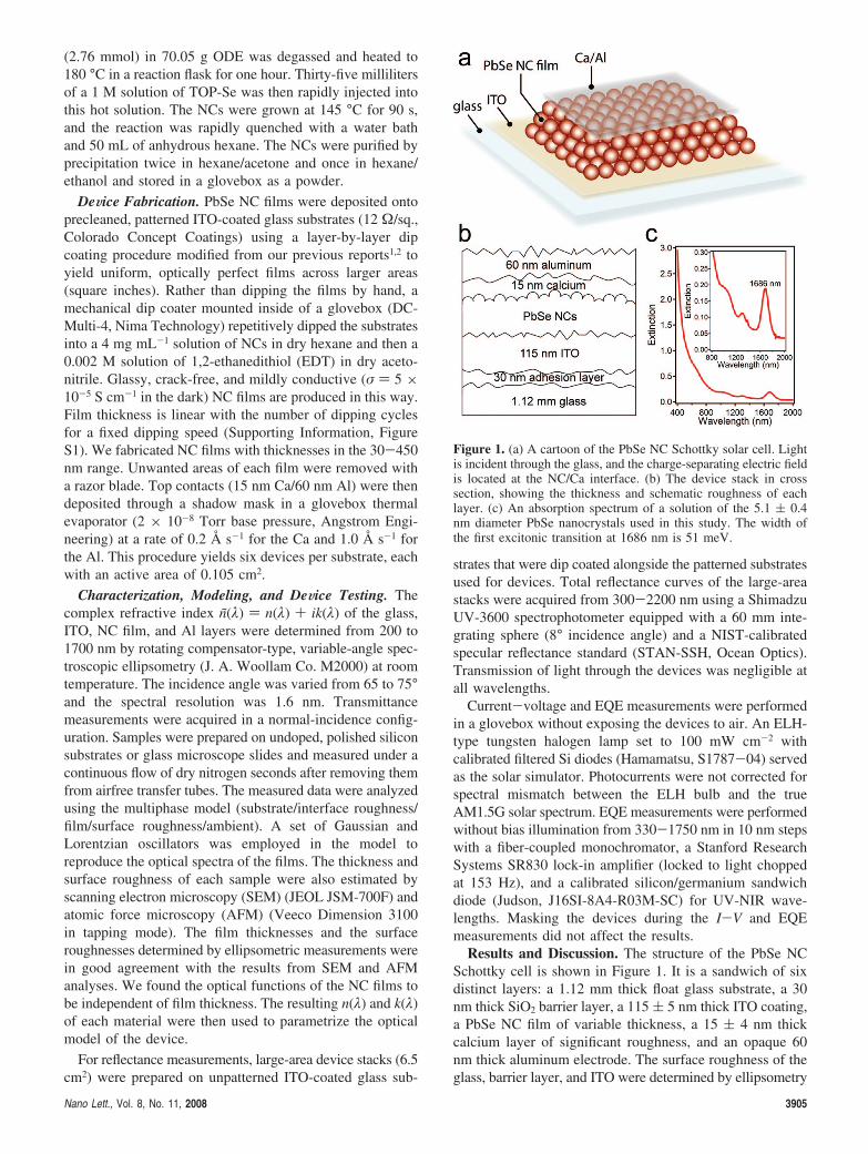
Results and Discussion. The structure of the PbSe NCSchottky cell is shown in Figure 1. It is a sandwich of sixdistinct layers: a 1.12 mm thick float glass substrate, a 30nm thick SiO2 barrier layer, a 115 ( 5 nm thick ITO coating,a PbSe NC film of variable thickness, a 15 ( 4 nm thickcalcium layer of significant roughness, and an opaque 60nm thick aluminum electrode. The surface roughness of theglass, barrier layer, and ITO were determined by ellipsometry
Figure 1. (a) A cartoon of the PbSe NC Schottky solar cell. Lightis incident through the glass, and the charge-separating electric fieldis located at the NC/Ca interface. (b) The device stack in crosssection, showing the thickness and schematic roughness of eachlayer. (c) An absorption spectrum of a solution of the 5.1 ( 0.4nm diameter PbSe nanocrystals used in this study. The width ofthe first excitonic transition at 1686 nm is 51 meV.
Nano Lett., Vol. 8, No. 11, 2008 3905

and AFM measurements to be 5-8 nm. Roughness at thePbSe/Ca and Ca/Al interfaces is approximately twice as greatbecause the NC film is granular and the calcium layerprobably exists as aggregated three-dimensional (3D) islandsrather than a smooth, conformal film.3 As we show below,the roughness of these layers should be taken into accountin order to achieve high-quality fits to the experimentalreflectance curves.
Our optical model is based on the 2 × 2 scattering matrixformalism of Pettersson et al. that calculates the opticalelectric field distribution within a device stack as a functionof depth and wavelength.4-12 The model assumes isotropicand homogeneous layers separated by plane parallel inter-faces. The inputs to the model include the index of refractionn(λ), extinction coefficient k(λ) and thickness of each layer,as well as the spectral irradiance, angle of incidence andpolarization of the illumination. Surface roughness is treatedby assigning a Gaussian spread to the thickness of each layeraccording to Lerondel et al.13 Reflections at the air/glassinterface and dispersion within the glass substrate are alsoincluded. The model yields the spectral reflectance F and
transmittance τ of the device, the absorptance R in each layer,and the number of photons absorbed (the generation rate G)as a function of wavelength and depth in the device. At eachwavelength, the average rate of photon absorption at adistance x into the device is proportional to the product ofthe modulus squared of the optical electric field E(λ, x), theindex of refraction n(λ, x) and the absorption coefficient R(λ,x), divided by the photon energy hν,
G(λ, x))cε0R(λ, x)n(λ, x)|E(λ, x)|2
2hV(1)
where R(λ, x) ) 4πk(λ, x)/λ.The model was parametrized with n(λ) and k(λ) values
calculated from spectroscopic ellipsometry data of thedifferent layers prepared on silicon or glass substrates andmeasured in air under a continuous flow of dry nitrogen.NC films of several thicknesses were measured to determineif the optical constants of the active layer depend onthickness. Figure 2 shows n(λ) and k(λ) of 80 and 185 nmthick NC films relative to the values for bulk PbSe.14 Notrends with thickness were identified. However, some scatter
Figure 2. The optical constants of PbSe NC films of two differentthicknesses (80 and 185 nm) relative to values for bulk PbSe (seeref 14). The NC data vary by less than 10% for 300-1000 nm, butk(λ) shows substantial relative variation from 1100-1600 nm(difficult to see because of the small magnitude of k(λ) in this regionof the spectrum).
Figure 3. Optical penetration depths of the different layers in thedevice stack.
Figure 4. Experimental and modeled reflectance curves of deviceswith NC film thicknesses from 0 to 260 nm (as determined by AFMand SEM). The incidence angle is 8°. The thickness and roughness(in parentheses) of the layers found by each nonlinear least-squaresfit are indicated. The fitting parameters were allowed to vary withinthe following limits: 110-125 nm ITO, 10-25 nm Ca, and 0-20nm rms interfacial roughness. All fits employed a 1.12 mm thickglass substrate and 30 nm adhesion layer with 5 nm of roughness.
3906 Nano Lett., Vol. 8, No. 11, 2008
in the optical constants was found, particularly for k(λ) inthe IR wavelengths, where k(λ) is small in magnitude andtherefore difficult to determine accurately with ellipsometry.The variation in n(λ) between the two films in Figure 2 isless than 10% across the spectrum, while the k(λ) valuesvary by less than 10% from 300-1000 nm but divergesomewhat into the near-IR. The film-to-film variation in theIR k(λ) values of the NC layers must be borne in mind wheninterpreting the IQE results from our model, as discussedbelow. The optical constants of calcium could not bedetermined by ellipsometry because calcium oxidizes toorapidly in air to allow reliable measurements; values fromliterature were used instead,15 and checked against reflectancemeasurements of glass/barrier/ITO/Ca stacks to ensure thatgood fits were obtained. The fits for both calcium andaluminum layers on ITO are provided in Figure S2 of theSupporting Information, which also contains a file of theoptical constants of each layer used in the model. Theresulting optical penetration depths [1/R(λ)] of the NC, ITO,Ca, and Al layers are compared in Figure 3.
The experimental and modeled reflectance curves of aseries of devices of different NC film thickness are presented
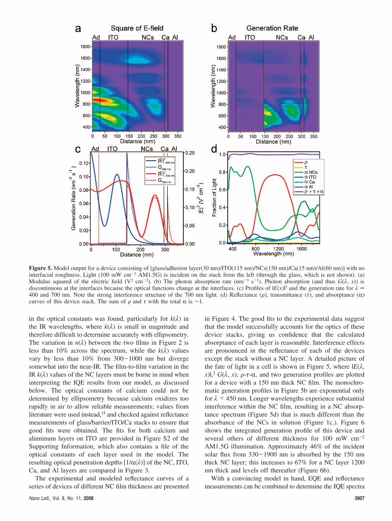
in Figure 4. The good fits to the experimental data suggestthat the model successfully accounts for the optics of thesedevice stacks, giving us confidence that the calculatedabsorptance of each layer is reasonable. Interference effectsare pronounced in the reflectance of each of the devicesexcept the stack without a NC layer. A detailed picture ofthe fate of light in a cell is shown in Figure 5, where |E(λ,x)|,2 G(λ, x), F-τ-R, and two generation profiles are plottedfor a device with a 150 nm thick NC film. The monochro-matic generation profiles in Figure 5b are exponential onlyfor λ < 450 nm. Longer wavelengths experience substantialinterference within the NC film, resulting in a NC absorp-tance spectrum (Figure 5d) that is much different than theabsorbance of the NCs in solution (Figure 1c.). Figure 6shows the integrated generation profile of this device andseveral others of different thickness for 100 mW cm-2
AM1.5G illumination. Approximately 46% of the incidentsolar flux from 330-1900 nm is absorbed by the 150 nmthick NC layer; this increases to 67% for a NC layer 1200nm thick and levels off thereafter (Figure 6b).
With a convincing model in hand, EQE and reflectancemeasurements can be combined to determine the IQE spectra
Figure 5. Model output for a device consisting of [glass/adhesion layer(30 nm)/ITO(115 nm)/NCs(150 nm)/Ca(15 nm)/Al(60 nm)] with nointerfacial roughness. Light (100 mW cm-2 AM1.5G) is incident on the stack from the left (through the glass, which is not shown). (a)Modulus squared of the electric field (V2 cm-2). (b) The photon absorption rate (nm-3 s-1). Photon absorption (and thus G(λ, x)) isdiscontinuous at the interfaces because the optical functions change at the interfaces. (c) Profiles of |E(x)|2 and the generation rate for λ )400 and 700 nm. Note the strong interference structure of the 700 nm light. (d) Reflectance (F), transmittance (τ), and absorptance (R)curves of this device stack. The sum of F and τ with the total R is ∼1.
Nano Lett., Vol. 8, No. 11, 2008 3907
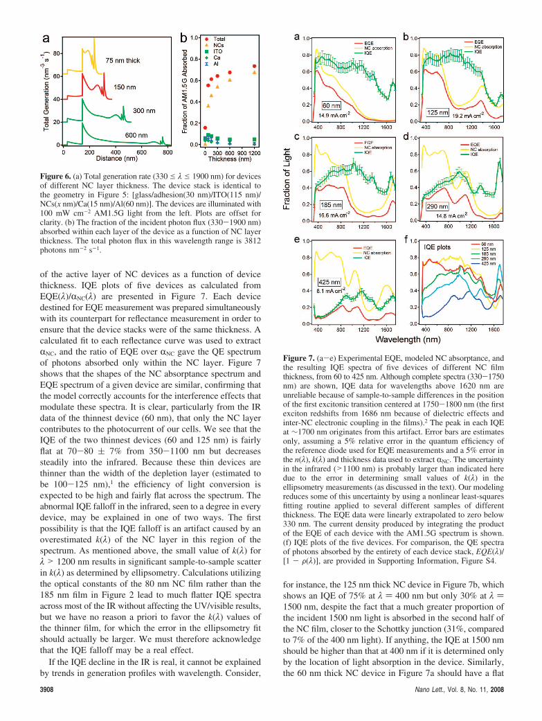
of the active layer of NC devices as a function of devicethickness. IQE plots of five devices as calculated fromEQE(λ)/RNC(λ) are presented in Figure 7. Each devicedestined for EQE measurement was prepared simultaneouslywith its counterpart for reflectance measurement in order toensure that the device stacks were of the same thickness. Acalculated fit to each reflectance curve was used to extractRNC, and the ratio of EQE over RNC gave the QE spectrumof photons absorbed only within the NC layer. Figure 7shows that the shapes of the NC absorptance spectrum andEQE spectrum of a given device are similar, confirming thatthe model correctly accounts for the interference effects thatmodulate these spectra. It is clear, particularly from the IRdata of the thinnest device (60 nm), that only the NC layercontributes to the photocurrent of our cells. We see that theIQE of the two thinnest devices (60 and 125 nm) is fairlyflat at 70-80 ( 7% from 350-1100 nm but decreasessteadily into the infrared. Because these thin devices arethinner than the width of the depletion layer (estimated tobe 100-125 nm),1 the efficiency of light conversion isexpected to be high and fairly flat across the spectrum. Theabnormal IQE falloff in the infrared, seen to a degree in everydevice, may be explained in one of two ways. The firstpossibility is that the IQE falloff is an artifact caused by anoverestimated k(λ) of the NC layer in this region of thespectrum. As mentioned above, the small value of k(λ) forλ > 1200 nm results in significant sample-to-sample scatterin k(λ) as determined by ellipsometry. Calculations utilizingthe optical constants of the 80 nm NC film rather than the185 nm film in Figure 2 lead to much flatter IQE spectraacross most of the IR without affecting the UV/visible results,but we have no reason a priori to favor the k(λ) values ofthe thinner film, for which the error in the ellipsometry fitshould actually be larger. We must therefore acknowledgethat the IQE falloff may be a real effect.
If the IQE decline in the IR is real, it cannot be explainedby trends in generation profiles with wavelength. Consider,
for instance, the 125 nm thick NC device in Figure 7b, whichshows an IQE of 75% at λ ) 400 nm but only 30% at λ )1500 nm, despite the fact that a much greater proportion ofthe incident 1500 nm light is absorbed in the second half ofthe NC film, closer to the Schottky junction (31%, comparedto 7% of the 400 nm light). If anything, the IQE at 1500 nmshould be higher than that at 400 nm if it is determined onlyby the location of light absorption in the device. Similarly,the 60 nm thick NC device in Figure 7a should have a flat
Figure 6. (a) Total generation rate (330e λe 1900 nm) for devicesof different NC layer thickness. The device stack is identical tothe geometry in Figure 5: [glass/adhesion(30 nm)/ITO(115 nm)/NCs(x nm)/Ca(15 nm)/Al(60 nm)]. The devices are illuminated with100 mW cm-2 AM1.5G light from the left. Plots are offset forclarity. (b) The fraction of the incident photon flux (330-1900 nm)absorbed within each layer of the device as a function of NC layerthickness. The total photon flux in this wavelength range is 3812photons nm-2 s-1.
Figure 7. (a-e) Experimental EQE, modeled NC absorptance, andthe resulting IQE spectra of five devices of different NC filmthickness, from 60 to 425 nm. Although complete spectra (330-1750nm) are shown, IQE data for wavelengths above 1620 nm areunreliable because of sample-to-sample differences in the positionof the first excitonic transition centered at 1750-1800 nm (the firstexciton redshifts from 1686 nm because of dielectric effects andinter-NC electronic coupling in the films).2 The peak in each IQEat ∼1700 nm originates from this artifact. Error bars are estimatesonly, assuming a 5% relative error in the quantum efficiency ofthe reference diode used for EQE measurements and a 5% error inthe n(λ), k(λ) and thickness data used to extract RNC. The uncertaintyin the infrared (>1100 nm) is probably larger than indicated heredue to the error in determining small values of k(λ) in theellipsometry measurements (as discussed in the text). Our modelingreduces some of this uncertainty by using a nonlinear least-squaresfitting routine applied to several different samples of differentthickness. The EQE data were linearly extrapolated to zero below330 nm. The current density produced by integrating the productof the EQE of each device with the AM1.5G spectrum is shown.(f) IQE plots of the five devices. For comparison, the QE spectraof photons absorbed by the entirety of each device stack, EQE(λ)/[1 - F(λ)], are provided in Supporting Information, Figure S4.
3908 Nano Lett., Vol. 8, No. 11, 2008
IQE spectrum because it is fully depleted and thereforeinsensitive to where light absorption occurs. The decreasinginfrared IQE observed for all device thicknesses suggeststhat photocurrent collection is governed by the photon energyas well as the generation profile at each wavelength.
We propose that the falloff in infrared IQE may occurbecause lower-energy photons produce cooler excitons thathave a greater tendency to recombine before escaping fromtheir parent NC. Visible photons, on the other hand, producerelatively high-energy excitons with a greater tendency todissociate into free carriers and delocalize throughout theNC film, thereby more efficiently contributing to photo-current. This type of energy-dependent branching ratio forthe production of excitons versus free carriers is commonlyobserved in conjugated polymers15,16 and is not an unexpectedfeature of electronically coupled NC solids in which eachNC acts as a potential energy well. However, additional workis needed to determine whether this effect is occurring inour NC devices.
As the thickness of the NC layer is increased, IQEperformance becomes progressively poorer overall, especiallyin the blue, because the layer thickness exceeds the sum ofthe depletion width and diffusion length such that a deadregion is established close to the ITO contact. The increasingIQE from 350-1000 nm (Figure 7c-e) is caused by thehigher recombination probability of excitons created byphotons absorbed closer to the ITO within this dead region.Referring to Figure 5b, we see that the fraction of lightabsorbed in the first half of the NC layer (nearest the ITO)decreases with increasing wavelength until λ ) 1000-1200nm. This trend is general for cells with NC layers 150-450nm thick (Supporting Information, Figure S3) and explainsthe positive slope of the visible IQE of our thicker devices.In summary, the IQE of the thicker devices at λ <1000-1200 nm is primarily determined by where light isabsorbed within each cell relative to the location of theelectric field of the Schottky junction.
The data set in Figure 7 enables us to comment on thetrends in solar cell performance as a function of device
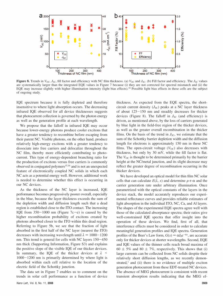
thickness. As expected from the EQE spectra, the short-circuit current density (JSC) peaks at a NC layer thicknessof about 125-150 nm and steadily decreases for thickerdevices (Figure 8). The falloff in JSC (and efficiency) isdriven, as mentioned above, by the loss of carriers generatedby blue light in the field-free region of the thicker devices,as well as the greater overall recombination in the thickerfilms. On the basis of the trend in JSC, we estimate that thesum of the Schottky barrier depletion width and the diffusionlength for electrons is approximately 150 nm in these NCfilms. The open-circuit voltage (VOC) also decreases withthickness, but only by 30 mV, while the fill factor is flat.The VOC is thought to be determined primarily by the barrierheight at the NC/metal junction, and its slight decrease mayreflect the greater degree of recombination occurring in thethicker devices.
We have developed an optical model for thin film NC solarcells that can calculate E(λ, x) and determine F-τ-R and thecarrier generation rate under arbitrary illumination. Onceparametrized with the optical constants of the layers in thedevice stack, the model accurately reproduces our experi-mental reflectance curves and provides reliable estimates oflight absorption in the individual ITO, NC, Ca, and Al layers.The shapes of the experimental EQE spectra agree well withthose of the calculated absorptance spectra; their ratios givewell-constrained IQE spectra that offer insight into theoperation of these devices. We find, first of all, thatinterference effects must be considered in order to calculatemeaningful generation profiles and IQE spectra. Generationprofiles of the Beer’s Law form, G(x) ) RI0e-Rx, are accurateonly for thicker devices at shorter wavelengths. Second, EQEand IQE values of the thinner cells reach broad maxima of60 ( 5% and 80 ( 7%, respectively. This shows that (i)large currents can be collected from NC solids despite theirrelatively short diffusion lengths, as we recently demon-strated,1 and (ii) there is no evidence of multiple excitongeneration photocurrent from these EDT-treated NC devices.The absence of MEG photocurrent is consistent with recenttransient absorption results indicating that the MEG ef-
Figure 8. Trends in VOC, JSC, fill factor and efficiency with NC film thickness. (a) VOC and JSC. (b) Fill factor and efficiency. The JSC valuesare systematically larger than the integrated EQE values in Figure 7 because (i) they are not corrected for spectral mismatch and (ii) theEQE may increase slightly with higher illumination intensity (light bias effects).18 Possible light bias effects in these cells are the subjectof ongoing study.
Nano Lett., Vol. 8, No. 11, 2008 3909

ficiency is very low in EDT-treated NC films.19 Strong inter-NC coupling caused by total removal of the original oleateligands during treatment with EDT2 may result in inter-NCcharge-transfer processes competing with multiexciton for-mation, thus lowering the MEG yield. Finally, the depen-dence of the IQE spectra on device thickness corroboratesthe back-contact Schottky model recently proposed by us1
and by Koleilat et al.20 to explain the operation of thesedevices. The decrease in the infrared IQE in Figure 7 maybe either an artifact or evidence that lower-energy photonstend to produce trapped excitons rather than free carriers.The optical model described here is applicable to planar thinfilm devices generally and will provide a powerful tool tooptimize future NC solar cell designs, particularly whencombined with a microscopic electrical model.
Acknowledgment. The authors thank Q. Song and B.Hughes for nanocrystal synthesis, B. To for AFM, D. Levifor assistance with ellipsometry, and D. Ginley for use ofthe glove boxes. M.C.B., J.M.L., and A.J.N. were supportedby the Chemical Sciences, Geosciences, and BiosciencesDivision of the Office of Basic Energy Science of the U.S.DOE, contract DE-AC36-99-GO10337; M.L. acknowledgessupport from the Energy Efficiency and Renewable EnergyPhotovoltaics Program.
Correspondence and requests for materials should beaddressed to M.L. or M.C.B.
Supporting Information Available: This material isavailable free of charge via the Internet at http://pubs.acs.org.
References(1) Luther, J. M.; Law, M.; Song, Q.; Reese, M. O.; Beard, M. C.;
Ellingson, R. J.; Nozik, A. J. in press.(2) Luther, J. M.; Law, M.; Song, Q.; Perkins, C. L.; Beard, M. C.; Nozik,
A. J. ACS Nano 2008, 2, 271–280.(3) No attempt was made to confirm Ca island growth on the NC film
with AFM because of the complications caused by rapid oxidation ofCa in air. However, a rough Ca layer is consistent with our modelingresults. Also, see Zhu, J.; Goetsch, P.; Ruzycki, N.; Campbell, C. T.J. Am. Chem. Soc. 2007, 129, 6432–6441.
(4) Pettersson, L. A. A.; Roman, L. S.; Inganas, O. J. Appl. Phys. 1999,86, 487–496.
(5) Pettersson, L. A. A.; Roman, L. S.; Inganas, O. J. Appl. Phys. 2001,89, 5564–5569.
(6) Peumans, P.; Yakimov, A.; Forrest, S. R. J. Appl. Phys. 2003, 93,3693–3723.
(7) Hoppe, H.; Arnold, N.; Meissner, D.; Sariciftci, N. S. Thin Solid Films2004, 451-452, 589–592.
(8) Persson, N. K.; Arwin, H.; Inganas, O. J. Appl. Phys. 2005, 97, 034503-(9) O’Connor, B.; An, K. H.; Pipe, K. P.; Zhao, Y.; Shtein, M. Appl.
Phys. Lett. 2006, 89, 233502.(10) Moule, A. J.; Bonekamp, J. B.; Meerholz, K. J. Appl. Phys. 2006,
100, 094503.(11) Sievers, D. W.; Shrotriya, V.; Yang, Y. J. Appl. Phys. 2006, 100,
114509.(12) Dennler, G.; Forberich, K.; Scharber, M. C.; Brabec, C. J.; Tomis, I.;
Hingerl, K.; Fromherz, T. J. Appl. Phys. 2007, 102, 054516.(13) Lerondel, G.; Romestain, R. Appl. Phys. Lett. 1999, 74, 2740–2742.(14) Suzuki, N.; Sawai, K.; Adachi, S. J. Appl. Phys. 1995, 77, 1249–
1255.(15) Arkhipov, V. I.; Emelianova, E. V.; Bassler, H. Phys. ReV. Lett. 1999,
82, 1321–1324.(16) Scheblykin, I. G.; Yartsev, A.; Pullerits, T.; Gulbinas, V.; Sundstrom,
V. J. Phys. Chem. B 2007, 111, 6303–6321.(17) Data for 300-900 nm were taken from (a) Ramsdale, C. M.;
Greenham, N. C. J. Phys. D 2003, 36, L29–L34. Data wereextrapolated into the NIR using (b) Potter, M. R.; Green, G. W. J.Phys. F: Metal Phys. 1975, 5, 1426.
(18) Hohl-Ebinger, J.; Hinsch, A.; Sastrawan, R.; Warta, W.; Wurfel, U.Proceedings of the 19th European Photovoltaic Solar Energy Confer-ence, Paris, 2004.
(19) Beard, M. C.; Midgett, A.; Law, M.; Nozik, A. J. National RenewableEnergy Laboratory, Golden, Colorado. Unpublished work, 2008.
(20) Koleilat, G. I.; Levina, L.; Shukla, H.; Myrskog, S. H.; Hinds, S.;Pattantyus-Abraham, A.; Sargent, E. H. ACS Nano 2008, 2, 833–840.
NL802353X
3910 Nano Lett., Vol. 8, No. 11, 2008