nano letters enhanced thermopower in pbse nanocrystal...
TRANSCRIPT

Enhanced Thermopower in PbSeNanocrystal Quantum Dot SuperlatticesRobert Y. Wang,† Joseph P. Feser,† Jong-Soo Lee,‡,§ Dmitri V. Talapin,*,‡,§
Rachel Segalman,*,| and Arun Majumdar*,†,⊥
Department of Mechanical Engineering, UniVersity of California,Berkeley, California 94720, The Molecular Foundry, Lawrence Berkeley NationalLaboratory, Berkeley, California 94720, Department of Chemistry, UniVersity ofChicago, Chicago, Illinois 60637, Department of Chemical Engineering, UniVersity ofCalifornia, Berkeley, California 94720, and Department of Materials Science andEngineering, UniVersity of California, Berkeley, California 94720
Received April 5, 2008; Revised Manuscript Received June 6, 2008
ABSTRACT
We examine the effect of strong three-dimensional quantum confinement on the thermopower and electrical conductivity of PbSe nanocrystalsuperlattices. We show that for comparable carrier concentrations PbSe nanocrystal superlattices exhibit a substantial thermopower enhancementof several hundred microvolts per Kelvin relative to bulk PbSe. We also find that thermopower increases monotonically as the nanocrystalsize decreases due to changes in carrier concentration. Lastly, we demonstrate that thermopower of PbSe nanocrystal solids can be tailoredby charge-transfer doping.
Developing low-cost and efficient thermoelectric materialsis a field of growing academic and technological interest.1,2
The performance of a thermoelectric material can be evalu-ated by its thermoelectric figure of merit, ZT ) S2σT/k, whereS is the Seebeck coefficient (also known as thermopower),σ is the electrical conductivity, k is the thermal conductivity,and T is the absolute temperature. It was predicted recentlythat low-dimensional materials can provide large values ofZT.3–5 Since then, several high-ZT nanostructured materialshave been reported.6–10 However, practical use of thesematerials is hampered by complicated and expensive syn-thesis techniques, such as molecular-beam epitaxy.7 Althoughimprovements in ZT for nanostructured materials havegenerally been attributed to reductions in thermal conductiv-ity,1,2 the unique electronic structure of low-dimensionalmaterials can also have a strong impact on thermopower andcharge transport.
Colloidal synthesis of monodisperse nanocrystals couldoffer a convenient route to low-cost and production-scalablelow-dimensional thermoelectric materials. Moreover, chemi-
cal synthesis allows precise tuning of the nanocrystal sizein the sub-10-nm range typically inaccessible for molecular-beam-epitaxy-grown quantum dots.11 This opens up thepossibility to explore thermoelectric properties of stronglyquantum-confined materials. In this regime, the valence andconduction bands of a semiconductor collapse into well-separated discrete energy states,2,12,13 which alters thefundamental properties of a semiconductor such as theelectronic density of states (DOS) and band-gap energy.2,12,13
Quantum confinement leads to sharp delta-function-likepeaks in the DOS, which is predicted by Mahan and Sofo14
to be the best possible electronic structure for a thermoelectricmaterial. Recent calculations by Humphrey and Linke15
predict that optimized nanostructured materials with a delta-function-like DOS can have ZT approaching 10 at roomtemperature. This exciting prediction originates from thefundamental difference between thermodynamics and trans-port in nanostructured materials as compared to bulkthermoelectric materials.15 It is also anticipated that thesematerials will have advantageous thermal properties becausethe nanocrystal diameters are much smaller than the phononmean free path (∼10-7 to 10-8 m for crystalline materials atroom temperature).16,17 This causes a strong suppression ofthermal conductivity due to phonon scattering at the nano-crystal boundaries.18,19 In our work, this extreme regime isrealized by using PbSe nanocrystal superlattices with varyingnanocrystal sizes.
* Corresponding authors. E-mail: [email protected]; [email protected]; [email protected].
† Department of Mechanical Engineering, University of California,Berkeley.
‡ The Molecular Foundry, Lawrence Berkeley National Laboratory.§ Department of Chemistry, University of Chicago.| Department of Chemical Engineering, University of California, Ber-
keley.⊥ Department of Materials Science and Engineering, University of
California, Berkeley.
NANOLETTERS
2008Vol. 8, No. 82283-2288
10.1021/nl8009704 CCC: $40.75 2008 American Chemical SocietyPublished on Web 07/03/2008

Charge transport in an array of close-packed semiconduc-tor nanocrystals separated by thin barriers can occur byhopping between quantum-confined orbitals with S and Psymmetry.20,21 To date, arrays of lead chalcogenide nano-crystals show the most promising charge transport properties.This is due to their monodispersity and eightfold degeneracyof 1S electron and hole states that allows good energy-levelalignment between adjacent particles, leads to sharp peaksin the electronic DOS, and provides a very large number ofelectronic states available for charge transport.22 The ex-traordinarily large static dielectric constant of PbSe (ε ∼ 250)brings down the charging energy and prevents Coulombblockade in PbSe nanocrystal solids.22,23 We demonstratedrecently that engineering interparticle spacing allows tuningof the exchange coupling energy and can increase carriermobility in self-assembled superlattices of PbSe nanocrystalsby many orders of magnitude approaching >1 cm2/Vs.22
Ultimately, further increases of quantum-mechanical couplingbetween individual nanocrystals packed into a long-rangeordered superlattice should lead to high-mobility Blochtransport through three-dimensional minibands.24 Lastly, bulklead chalcogenides are used widely in commercial thermo-electric devices due to the combination of S, σ, and kparameters naturally favoring large values of ZT.
PbSe nanocrystals of different size were synthesized byreacting lead oleate with tri-n-octylphosphine selenide insqualane in the presence of oleic acid capping ligands.22 Wevaried the size of the nanocrystals from ∼4.3 to ∼8.6 nmwhile keeping the size distribution well below 10%. Thenarrow size distribution allows the resolution of the sharpexcitonic features in the absorption spectra of the colloidalsolutions and can also be seen in the transmission electronmicroscopy images (Figure 1a). Prior to nanocrystal filmdeposition, glass substrates were treated with hexamethyldisilazane to improve the wetting properties. Films of
monodisperse PbSe nanocrystals were deposited by drop-casting hexane/octane (9:1 by volume) solutions on substrateswith preformed parallel Cr/Au electrodes (Figure 1b). Theresulting film thickness was generally 50-200 nm. The PbSenanocrystals are initially coated with oleic acid ligands. Afterdrop-casting, the oleic acid is removed by hydrazine treat-ment as described in ref 22 (NOTE: hydrazine is toxic andshould be handled using appropriate protective equip-ment to prevent contact with either the vapors or theliquid). Hydrazine molecules replace oleic acid at thenanocrystal surface, which reduces the interparticle spacingfrom ∼1.1 nm down to 0.4 nm and results in greatlyimproved electrical conductivity.22 Hydrazine treatment doesnot change the nanocrystal’s size and shape (Figure 1c);treated nanocrystal films possess characteristic excitonicfeatures in the absorption spectrum.22
Unless stated otherwise, all nanocrystal superlattices werekept inside a dry-nitrogen glovebox during storage andmeasurements. Temperature gradients for the thermopowermeasurements were created with commercially availablethermoelectric devices. Voltages and temperatures weremeasured with an Agilent 34401a voltmeter and thermo-couples, respectively. The temperature gradient was modu-lated by varying the electrical current to the thermoelectricdevices. After hydrazine treatment, the thermopower andconductivity of the nanocrystal film exhibited a strong time-dependence that asymptotes. We attribute this time-depen-dence to the changes in hydrazine concentration in thenanocrystal solid (vide infra). The length of this transienceincreased for smaller nanocrystal sizes and generally variedbetween 1 and 15 days. Unless indicated otherwise, the datapresented is taken at the asymptote of this transience.
When a temperature gradient, (|∆T | ) 0-30 K) is createdacross the nanocrystal film, an open circuit voltage Voc
proportional to the temperature gradient is observed (Figure2a). The Seebeck coefficient is given by -dVoc/dT (e.g., apositive Seebeck coefficient implies that the cold regiondevelops a higher potential than the hot region). Thedependence on nanocrystal size for thermopower is shownin Figure 2b. As the nanocrystal size decreases from 8.6 to4.8 nm, the thermopower increases from 700 to 1150 µV/K.The positive sign of thermopower indicates that transport inthese films is p-type. A combination of electrical conductivityand field-effect transistor measurements provide insight intothese thermopower results. Over the same nanocrystal sizerange, we observed a drop in electrical conductivity by about1 order of magnitude (Figure 2c). Field-effect hole mobilitywas ∼0.l cm2/V-s and no nanocrystal size dependence wasobserved (Figure S1 from Supporting Information). Usingthe mobility data, we can calculate the carrier concentrationin our nanocrystal solids because σ ) neµ, where µ is themobility, e is the electron charge, and n is the carrierconcentration. The carrier concentrations in Figure 2 arerepresentative of the entire film volume. Simple estimatesyield ∼0.2 carriers/dot for the 8.6 nm nanocrystals and∼0.002 carriers/dot for the 4.3 nm nanocrystals. For com-parable carrier concentrations, the PbSe nanocrystal film
Figure 1. (a) Absorption spectra of PbSe nanocrystals dispersedin tetrachloroethylene. The diameters are 4.8 (black), 5.6 (green),6.4 (red), 7.1 (blue), and 8.6 nm (pink). The electronic structure ofPbSe depends on the particle size due to quantum confinement.The inset shows the transmission electron microscopy image ofPbSe nanocrystals with diameter ∼7.1 nm. (b) The measurementdevice consisted of a glass wafer with two Cr/Au electrodes. (c)Typical high-resolution scanning electron microscopy image of aconductive PbSe nanocrystal film used in this study.
2284 Nano Lett., Vol. 8, No. 8, 2008
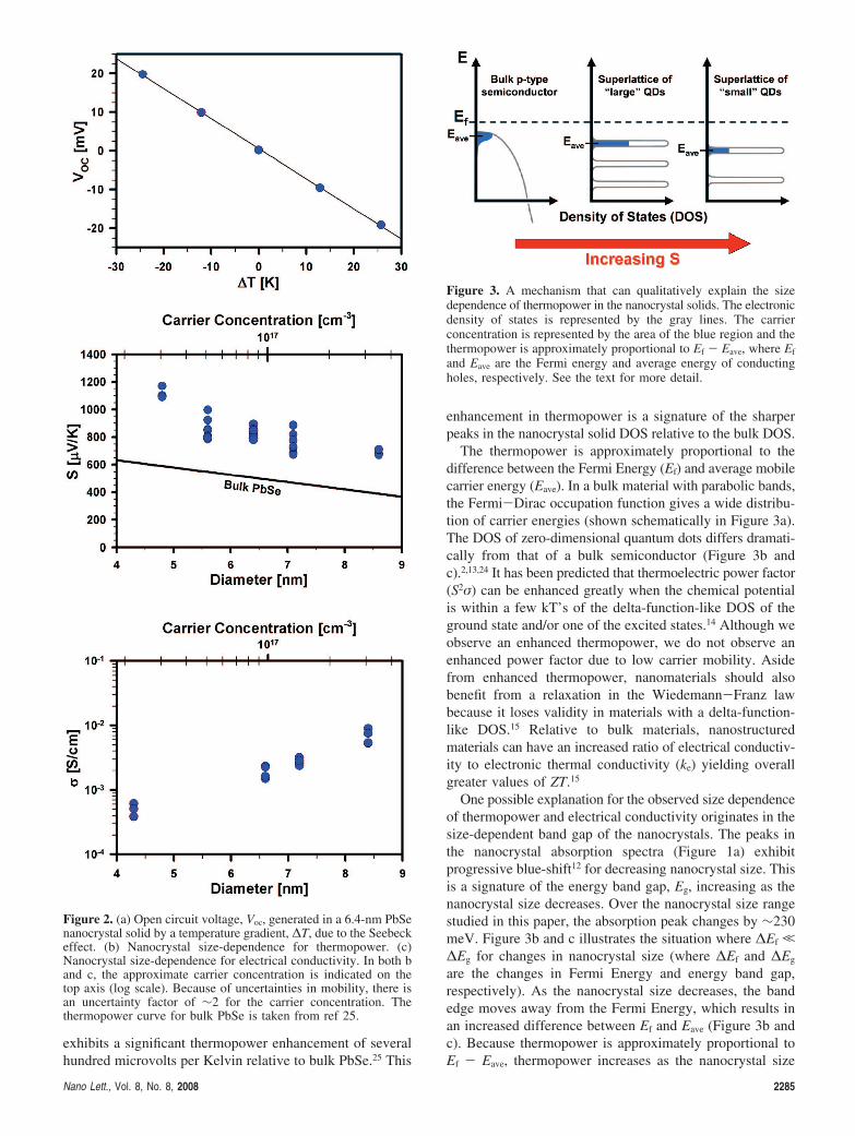
exhibits a significant thermopower enhancement of severalhundred microvolts per Kelvin relative to bulk PbSe.25 This
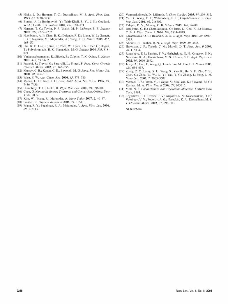
enhancement in thermopower is a signature of the sharperpeaks in the nanocrystal solid DOS relative to the bulk DOS.
The thermopower is approximately proportional to thedifference between the Fermi Energy (Ef) and average mobilecarrier energy (Eave). In a bulk material with parabolic bands,the Fermi-Dirac occupation function gives a wide distribu-tion of carrier energies (shown schematically in Figure 3a).The DOS of zero-dimensional quantum dots differs dramati-cally from that of a bulk semiconductor (Figure 3b andc).2,13,24 It has been predicted that thermoelectric power factor(S2σ) can be enhanced greatly when the chemical potentialis within a few kT’s of the delta-function-like DOS of theground state and/or one of the excited states.14 Although weobserve an enhanced thermopower, we do not observe anenhanced power factor due to low carrier mobility. Asidefrom enhanced thermopower, nanomaterials should alsobenefit from a relaxation in the Wiedemann-Franz lawbecause it loses validity in materials with a delta-function-like DOS.15 Relative to bulk materials, nanostructuredmaterials can have an increased ratio of electrical conductiv-ity to electronic thermal conductivity (ke) yielding overallgreater values of ZT.15
One possible explanation for the observed size dependenceof thermopower and electrical conductivity originates in thesize-dependent band gap of the nanocrystals. The peaks inthe nanocrystal absorption spectra (Figure 1a) exhibitprogressive blue-shift12 for decreasing nanocrystal size. Thisis a signature of the energy band gap, Eg, increasing as thenanocrystal size decreases. Over the nanocrystal size rangestudied in this paper, the absorption peak changes by ∼230meV. Figure 3b and c illustrates the situation where ∆Ef ,∆Eg for changes in nanocrystal size (where ∆Ef and ∆Eg
are the changes in Fermi Energy and energy band gap,respectively). As the nanocrystal size decreases, the bandedge moves away from the Fermi Energy, which results inan increased difference between Ef and Eave (Figure 3b andc). Because thermopower is approximately proportional toEf - Eave, thermopower increases as the nanocrystal size
Figure 2. (a) Open circuit voltage, Voc, generated in a 6.4-nm PbSenanocrystal solid by a temperature gradient, ∆T, due to the Seebeckeffect. (b) Nanocrystal size-dependence for thermopower. (c)Nanocrystal size-dependence for electrical conductivity. In both band c, the approximate carrier concentration is indicated on thetop axis (log scale). Because of uncertainties in mobility, there isan uncertainty factor of ∼2 for the carrier concentration. Thethermopower curve for bulk PbSe is taken from ref 25.
Figure 3. A mechanism that can qualitatively explain the sizedependence of thermopower in the nanocrystal solids. The electronicdensity of states is represented by the gray lines. The carrierconcentration is represented by the area of the blue region and thethermopower is approximately proportional to Ef - Eave, where Ef
and Eave are the Fermi energy and average energy of conductingholes, respectively. See the text for more detail.
Nano Lett., Vol. 8, No. 8, 2008 2285

decreases. This process also results in changes of carrierconcentration; larger carrier concentrations are obtained whenEf is near the band edge. As the nanocrystal size increases,the band edge moves closer to Ef. This causes the carrierconcentration (and therefore the electrical conductivity) toincrease. This explanation is further supported by the factthat mobility did not change with nanocrystal size, whichimplies that the observed changes in conductivity (Figure2c) are due to variations in carrier concentration. Anotherplausible explanation for thermopower size dependence isalteration of the scattering mechanisms that occur in nano-structured materials, which can lead to carrier-energy filter-ing.26
In the case of PbSe quantum wells, the thermopower andelectrical conductivity were found to oscillate with wellthickness.27 In contrast, we observe monotonic changes inthermopower and electrical conductivity. This paper reportsthe first thermopower measurements of solution-processedlow-dimensional materials in the regime of strong quantumconfinement. The observed size dependence creates op-portunities to tune the thermopower in these materials.
Besides obvious interest to thermoelectric applications ofnanocrystal solids, thermopower measurements are provento be a very powerful technique in fundamental studies ofelectronic structure and doping of bulk materials. In par-ticular, it can unambiguously point to the type of carriersresponsible for charge transport and provide valuable infor-mation on the Fermi energy under particular experimentalconditions. Because thermopower is measured under open-circuit conditions, it is not affected by contact resistance. Incontrast, the data obtained by current measurements in thefield-effect transistor configuration are strongly affected bynature of the contacts formed between the channel andelectrodes. For example, single-wall carbon nanotubescontacted by Au or Pd electrodes show a p-type gate effect,28
whereas the nanotubes contacted by a metal with low workfunction (e.g., Sc) show an n-type gate effect due to moreefficient electron injection.29 PbSe nanocrystal solids showp-type gate effect (Figure 4b), which is also expected fromcomparison of the work function and ionization potential ofAu and bulk PbSe (Figure 4d). Alternatively, a positivethermopower shows that the Fermi level in a PbSe nano-crystal solid is close to the 1Sh quantum-confined state andthat the nanocrystal array is p-doped. The detailed under-standing of electronic doping and conduction mechanism innanocrystal solids requires further study; a plausible hypoth-esis could be the presence of surface states behaving asshallow hole acceptors. These states are probably associatedwith undercoordinated or oxidized surface Se atoms whichare known to create the acceptor states in bulk PbSe.30 Analternative explanation could be the direct hopping betweenlocalized midgap surface states. From general considerations,observed hole mobilities (∼0.1 cm2/Vs) are somewhat toohigh for the hopping between trap states with localized wavefunctions that are separated by a dielectric medium. To gaina better understanding of the conduction in hydrazine-treatedPbSe nanocrystal solids, we measured the temperaturedependence for low-bias conduction (VDS < 200mV) in
N2H4-treated 7.2-nm PbSe nanocrystal solids. In the 200-310K temperature range, the film conduction is well describedby activated transport with the activation energy EA. Wefound that EA strongly depends on the applied gate voltage(VG), varying from 200 meV (VG ) 40V) down to 85 meV(VG ) 0V) and 28 meV (VG ) -40V). Following theanalysis by Mentzel et al., we estimate the depth of theacceptor states as ∼50-70 meV at room temperature.30
Thermal energy is required to generate a hole in the
Figure 4. (a and b) Transistor measurements on 8.5-nm PbSenanocrystal solids: plots of the current between drain and sourceelectrodes (IDS) versus drain-source voltage (VDS), as a functionof gate voltage (VG). Device channel length is 10 µm, width 3000µm, and the thickness of SiO2 gate dielectric is 100 nm. In thepresence of hydrazine, the nanocrystal solid exhibits an n-type gateeffect (a) whereas removal of hydrazine in vacuum switches thedevice to a p-type gate effect (b). (c) Monitoring of the thermopowerof a PbSe nanocrystal solid during hydrazine addition/removal(nanocrystal diameter ∼9.2 nm, film thickness ∼500 nm). At t )0 h, the sample had a steady-state thermopower of 685 µV/K. Afew drops of 1 M hydrazine in acetonitrile were added at t ) 0 hand t ) 39 h. With the addition of hydrazine, the PbSe nanocrystalsolid switches from p-type (S > 0) to n-type (S < 0). See the textfor more detail. (d) Energy diagram proposed for PbSe nanocrystalsolid in contact with Au electrodes on the basis of combinedtransport and thermopower measurements.
2286 Nano Lett., Vol. 8, No. 8, 2008

nanocrystal from the acceptor state providing the mobilecarrier in the 1Sh state. For a 60-meV-deep trap, theionization probability at room temperature is about 10-1.The DOS at the Fermi energy can be estimated as DOS(EF)) Ci/es (∆EF/∆VG)-1 where Ci is the capacitance of the gatedielectric per unit area, s is the screening length in thenanocrystal solid, and e is the electron charge.30 For 100-nm-thick SiO2 gate dielectric Ci ∼ 3.4 × 10⁻⁸ F cm-2. ∆EF/∆VG ∼ 3.1 × 10⁻³ eV V-1 was obtained from thedependence of the activation energy on VG. The possibilityto efficiently operate the 35-nm-thick transistor channel inthe depletion mode22 shows that the screening length s is asat least 20 nm. These parameters yield DOS(EF) < 3 × 10¹⁹/eV cm-3 at VG ) 0V, that is, less than 0.5 electronicallyactive acceptor states per nanocrystal and more than an orderof magnitude lower than the DOS associated with S-typequantum-confined orbitals. The localization length, a, formidgap states is small (∼1 nm) compared to that for S states(∼nanocrystal radius, ∼3.6 nm). The probability of hoppingbetween two states with similar energy is proportional to P∼ exp(-2d/a) where d is the hopping distance.31 For d ∼ 8nm, which is a reasonable estimate for our nanocrystal solid,the probability of hopping between localized midgap statesshould be ∼5 orders of magnitude lower than the hoppingprobability for more-delocalized S states. These argumentsseem to strongly support the transport through quantum-confined orbitals, not through the surface states.
To control the p-type doping level, we exposed a film of6.4-nm PbSe nanocrystals to oxygen, which is a well-knownp-dopant of bulk lead chalcogenides.32 After the exposure,we observed an increase in the conductivity of PbSenanocrystal film by about 1 order of magnitude (Figure S2from the Supporting Information) accompanied with adecrease in thermopower from 760 to 440 µV/K (Figure S3from the Supporting Information). After exposure to oxygenthe nanocrystal solid showed weak gating and electricalmeasurements alone could not separate the conductivityincrease due to changes of carrier mobility and/or dopinglevel. The decrease in thermopower points to a shifting ofthe Fermi Energy closer to the 1Sh state due to the dopingeffect.
We also used thermopower measurements to study thecharacteristics of n-type surface charge-transfer doping ofPbSe nanocrystals with hydrazine. Thermopower was moni-tored continuously as the relative amount of hydrazine in ananocrystal thin film was varied. This experiment is depictedin Figure 4c. At t ) 0 h, the sample had a steady-statethermopower of ∼685 µV/K, and a few drops of 1 Mhydrazine in acetonitrile are placed on the film. The dropletsevaporate after a few minutes, and a sharp transition fromp-type (S > 0) to n-type (S < 0) is observed simultaneously.A slow transition back to p-type is observed over the courseof many hours. We attribute this slow transition to evapora-tion of hydrazine from the nanocrystal film. These resultsconclusively show that n-doping of PbSe nanocrystal solidsis determined by hydrazine adhered to the nanocrystalsurface. The n-type doping occurs through the formation ofcharge-transfer complex between the nanocrystal and hy-
drazine molecules. Reversible behavior is demonstrated whenwe repeat the hydrazine treatment at t ) 39 h. The transistormeasurements on similarly treated PbSe nanocrystal filmsshow n-type gate effects in the presence of hydrazine (Figure4a), slowly switching to ambipolar and, finally, p-type gateeffect after removal of hydrazine (Figure 4b). Becausethermopower measurements are open circuit, they removethe possibility of the effects associated with nonideal contactbehavior. Figure 4c also shows that hydrazine-doped PbSenanocrystal solids can reach large negative thermopowers(ca. -650 µV/K), considerably exceeding values reportedfor n-PbSe.32
This works demonstrates that PbSe nanocrystal solidsexhibit a significant thermopower enhancement of severalhundred microvolts per Kelvin relative to bulk PbSe. Thiscan be attributed to the sharp peaks in the electronic DOSof nanocrystal solids. Tunability of thermopower via changesin nanocrystal size has also been demonstrated. If theelectrical conductivity can be improved, then these materialsrepresent an emerging class of inexpensive and scalablethermoelectric materials. This can be done by either increas-ing the carrier concentration or improving mobility. Increas-ing carrier concentration generally results in a decrease inthermopower, but could enhance ZT up until a maximumS2n is reached. This maximum value has not been achievedin this work and remains unknown. A more-promising routeto improve ZT is to improve mobility (e.g., reduce carrierscattering). To compete with commercial thermoelectricmaterials, the carrier mobility in nanocrystal solids shouldbe increased by at least 2-3 orders of magnitude. Further-more, if the reduction in carrier scattering has a favorableenergy dependence, then the thermopower could be enhanceddue to energy-filtering as in ref 26. In this ideal case,electrical conductivity and thermopower could be enhancedsimultaneously. Colloidal nanocrystals embedded in a hostmaterial would be an interesting system that may exhibit areduction in carrier scattering.
Acknowledgment. We acknowledge the support of theDivision of Materials Sciences and Engineering, Office ofBasic Energy Sciences, DOE. We thank the UC BerkeleyMicrofabrication Laboratory for the use of their facilities.R.Y.W. gratefully acknowledges a NSF IGERT fellowship.Work at the Molecular Foundry was supported by the U.S.Department of Energy under Contract No. DE-AC02-05CH11231. D.V.T. acknowledges NSF MRSEC programunder Award No. DMR-0213745.
Supporting Information Available: Materials and meth-ods and supplementary figures. This material is available freeof charge via the Internet at http://pubs.acs.org.
References(1) Chen, G.; Dresselhaus, M. S.; Dresselhaus, G.; Fleurial, J. P.; Caillat,
T. Int. Mater. ReV. 2003, 48, 45–66.(2) Dresselhaus, M. S.; Chen, G.; Tang, M. Y.; Yang, R. G.; Lee, H.;
Wang, D. Z.; Ren, Z. F.; Fleurial, J. P.; Gogna, P. AdV. Mater. 2007,19, 1043–1053.
(3) Hicks, L. D.; Dresselhaus, M. S. Physical ReView B 1993, 47, 16631–16634.
(4) Hicks, L. D.; Dresselhaus, M. S. Physical ReView B 1993, 47, 12727–12731.
Nano Lett., Vol. 8, No. 8, 2008 2287
(5) Hicks, L. D.; Harman, T. C.; Dresselhaus, M. S. Appl. Phys. Lett.1993, 63, 3230–3232.
(6) Boukai, A. I.; Bunimovich, Y.; Tahir-Kheli, J.; Yu, J. K.; Goddard,W. A.; Heath, J. R. Nature 2008, 451, 168–171.
(7) Harman, T. C.; Taylor, P. J.; Walsh, M. P.; LaForge, B. E. Science2002, 297, 2229–2232.
(8) Hochbaum, A. I.; Chen, R. K.; Delgado, R. D.; Liang, W. J.; Garnett,E. C.; Najarian, M.; Majumdar, A.; Yang, P. D. Nature 2008, 451,163–U5.
(9) Hsu, K. F.; Loo, S.; Guo, F.; Chen, W.; Dyck, J. S.; Uher, C.; Hogan,T.; Polychroniadis, E. K.; Kanatzidis, M. G. Science 2004, 303, 818–821.
(10) Venkatasubramanian, R.; Siivola, E.; Colpitts, T.; O’Quinn, B. Nature2001, 413, 597–602.
(11) Franchi, S.; Trevisi, G.; Seravalli, L.; Frigeri, P. Prog. Cryst. GrowthCharact. Mater. 2003, 47, 166–195.
(12) Murray, C. B.; Kagan, C. R.; Bawendi, M. G. Annu. ReV. Mater. Sci.2000, 30, 545–610.
(13) Wise, F. W. Acc. Chem. Res. 2000, 33, 773–780.(14) Mahan, G. D.; Sofo, J. O. Proc. Natil. Acad. Sci. U.S.A. 1996, 93,
7436–7439.(15) Humphrey, T. E.; Linke, H. Phys. ReV. Lett. 2005, 94, 096601.(16) Chen, G. Nanoscale Energy Transport and ConVersion; Oxford: New
York, 2005.(17) Kim, W.; Wang, R.; Majumdar, A. Nano Today 2007, 2, 40–47.(18) Prasher, R. Physical ReView B 2006, 74, 165413.(19) Wang, R. Y.; Segalman, R. A.; Majumdar, A. Appl. Phys. Lett. 2006,
89, 173113.
(20) Vanmaekelbergh, D.; Liljeroth, P. Chem Soc ReV 2005, 34, 299–312.(21) Yu, D.; Wang, C. J.; Wehrenberg, B. L.; Guyot-Sionnest, P. Phys.
ReV. Lett. 2004, 92, 216802.(22) Talapin, D. V.; Murray, C. B. Science 2005, 310, 86–89.(23) Ben-Porat, C. H.; Cherniavskaya, O.; Brus, L.; Cho, K. S.; Murray,
C. B. J. Phys. Chem. A 2004, 108, 7814–7819.(24) Lazarenkova, O. L.; Balandin, A. A. J. Appl. Phys. 2001, 89, 5509–
5515.(25) Abrams, H.; Tauber, R. N. J. Appl. Phys. 1969, 40, 3868.(26) Heremans, J. P.; Thrush, C. M.; Morelli, D. T. Phys. ReV. B 2004,
70, 115334.(27) Rogacheva, E. I.; Tavrina, T. V.; Nashchekina, O. N.; Grigorov, S. N.;
Nasedkin, K. A.; Dresselhaus, M. S.; Cronin, S. B. Appl. Phys. Lett.2002, 80, 2690–2692.
(28) Javey, A.; Guo, J.; Wang, Q.; Lundstrom, M.; Dai, H. J. Nature 2003,424, 654–657.
(29) Zhang, Z. Y.; Liang, X. L.; Wang, S.; Yao, K.; Hu, Y. F.; Zhu, Y. Z.;Chen, Q.; Zhou, W. W.; Li, Y.; Yao, Y. G.; Zhang, J.; Peng, L. M.Nano Lett. 2007, 7, 3603–3607.
(30) Mentzel, T. S.; Porter, V. J.; Geyer, S.; MacLean, K.; Bawendi, M. G.;Kastner, M. A. Phys. ReV. B 2008, 77, 075316.
(31) Mott, N. F. Conduction in Non-Crystalline Materials; Oxford: NewYork, 1993.
(32) Rogacheva, E. I.; Tavrina, T. V.; Grigorov, S. N.; Nashchenkina, O. N.;Volobuev, V. V.; Fedorov, A. G.; Nasedkin, K. A.; Dresselhaus, M. S.J. Electron. Mater. 2002, 31, 298–303.
NL8009704
2288 Nano Lett., Vol. 8, No. 8, 2008