development of nb and alternative material thin …development of nb and alternative material thin...
TRANSCRIPT
DEVELOPMENT OF NB AND ALTERNATIVE MATERIAL THIN FILMS TAILORED FOR SRF APPLICATIONS*
A.-M. Valente-Feliciano#, H. L. Phillips, C. E. Reece, J. Spradlin and X. Zhao, Thomas Jefferson National Accelerator Facility, Newport News, VA U.S.A.
F. Stevie, D. Batchelor, North Carolina State University, Raleigh, VA U.S.A. R. A. Lukaszew, B. Xiao, College William & Mary, Williamsburg, VA U.S.A.
Abstract Over the years, Nb/Cu technology, despite its
shortcomings due to the commonly used magnetron sputtering, has positioned itself as an alternative route for the future of superconducting structures used in accelerators. Recently, significant progress has been made in the development of energetic vacuum deposition techniques, showing promise for the production of thin films tailored for superconducting radio-frequency (SRF) applications. JLab is pursuing energetic condensation deposition via techniques such as Electron Cyclotron Resonance and High Power Impulse Magnetron Sputtering (HiPIMS). As part of this project, the influence of the deposition energy on the material and RF properties of the Nb thin film is investigated with the characterization of their surface, structure, superconducting properties and RF response. It has been shown that the film RRR can be tuned from single digits to values greater than 400. This paper presents results on surface impedance measurements correlated with surface and material characterization for Nb films produced on various substrates, monocrystalline and polycrystalline as well as amorphous. A progress report on work on NbTiN and AlN based multilayer structures will also be presented.
THIN FILMS APPLIED TO SRF In recent years, SRF cavities using Nb have reached RF
performances approaching its theoretical limit (Hc~180mT at 2K) [1]. Any further dramatic improvement in SRF performance or system cost reduction will necessarily come via the use of improved or alternative materials. Two opportunities are available for the development of SRF films: the engineering of “bulk like” Nb films and the development of multilayered SRF film structures.
Nb films Due to the very shallow penetration depth of RF fields
(~40nm for Nb), one can foresee the merits of depositing an Nb film on the inner surface of a castable cavity structure made of copper (Cu) or aluminium (Al). At the system design level, this would allow decoupling the active SRF surface from the accelerating structure definition and cooling, opening the possibility to dramatically change the cost framework of SRF accelerators.
Pioneering studies [2-4] conducted at CERN in the field of SRF Nb on Cu (Nb/Cu) film cavities and their successful implementation in LEP-2 have demonstrated the viability of this technology. Although gradients up to 25MV/m were achieved [5], these cavities suffered from losses resulting in the significant reduction of their quality factor Q at accelerating gradients above 15MV/m.
Several material factors, highly dependent upon the surface creation conditions, may contribute to degraded SRF performance. These limiting factors such as intra-granular and inter-granular impurities, lattice defect density, surface topography and chemistry, may lead to the reduction of the electron mean free path, thus the reduction of the lower critical field Hc1. Fundamental work is needed to establish the relative contribution of each of these factors and the correlation of detailed material characteristics with the resulting SRF performance.
SIS multilayer films A few years ago, a concept was proposed [6] which
would allow taking advantage of high-Tc superconductors without being penalized by their lower Hc1. The idea is to coat SRF cavities with alternating superconducting and insulating (SIS) layers with a thickness d smaller than the penetration depth λ so the Meissner state can be retained at a magnetic field much higher than the bulk Hc1. The thin higher-Tc layers provide magnetic screening of the bulk superconducting cavity delaying vortex penetration. The BCS resistance is also strongly reduced because the superconducting materials foreseen (Nb3Sn, NbTiN …) have a higher gap Δ than Nb. With such structures, Q-values at 4.2K could be increased two orders of magnitude above Nb values.
Approach JLab with neighbouring partners is pursuing both
opportunities. The primary focus is to understand the characteristics of the films produced, the nucleation and influence of the diverse deposition parameters, substrate nature, temperature and morphology on the final RF surface for Nb and multilayer films.
The quality of the resultant thin film is heavily influenced by the deposition technique utilized. With the availability of energetic condensation techniques, films with a wide range of microstructural properties and features believed to be relevant to RF performance can be produced, characterized and RF tested. In this context, _________________________________________
*Authored by Jefferson Science Associates, LLC under U.S. DOE Contract No. DE-AC05-06OR23177. The U.S. Government retains a non-exclusive, paid-up, irrevocable, world-wide license to publish or reproduce this manuscript for U.S. Government purposes. #[email protected]
Proceedings of IPAC2011, San Sebastián, Spain MOPC116
07 Accelerator Technology
T07 Superconducting RF 349 Cop
yrig
htc ○
2011
byIP
AC
’11/
EPS
-AG
—cc
Cre
ativ
eC
omm
onsA
ttri
butio
n3.
0(C
CB
Y3.
0)
JLab is using an Electron Cyclotron Resonance (ECR) Nb ion source in ultra-high vacuum (UHV) [7]. The main advantages are the production of a high flux of singly charged ions with controllable kinetic energy and the absence of macro-particle production. For the multilayer structures development, both reactive magnetron sputtering and high power impulse magnetron sputtering (HiPIMS) [8] are pursued.
ENGINEERED NIOBIUM FILMS The challenge is to develop an understanding of the
film growth dynamics from its nucleation to the final exposed surface. The defect density within the RF penetration depth determines the electron mean free path in that layer. It is certainly affected by contaminants incorporated during the final stage film growth, but it is also strongly affected by the underlying crystal texture developed from the initial film nucleation process and the substrate. The development of every stage can be expected to depend strongly on the kinetic energy of the arriving Nb ions.
Quality Nb structure via energetic condensation
Nb growth is being studied on various substrates, insulating, metallic and amorphous, single crystal and polycrystalline.
The resulting film structures confirm that the films characteristics are determined in the early stages of growth by the substrate parameters and the ion incident energy [9]. The on-going studies show that hetero-epitaxy of Nb on insulating and metallic crystalline substrates is easily achievable with high crystalline character and at temperatures low enough to maintain the mechanical integrity of the substrate [10, 11]. With sufficient energy provided (for a given Nb-substrate system) by the incident ions and the substrate temperature, films grow along the close-packed plane (110). Film roughness is in general low in the limit of the substrate roughness.
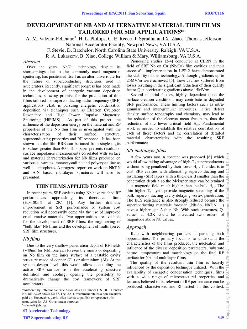
Low hydrogen content Because the ions are produced in UHV and the film
surface can be passivated in-situ by oxidation, the amount of impurities embedded in the films can be controlled. As an example, SIMS analyses show that the hydrogen content of ECR films (Fig. 1a) is significantly lower than for standard high RRR Nb (Fig. 1b) treated with the conventional wet chemistry processes.
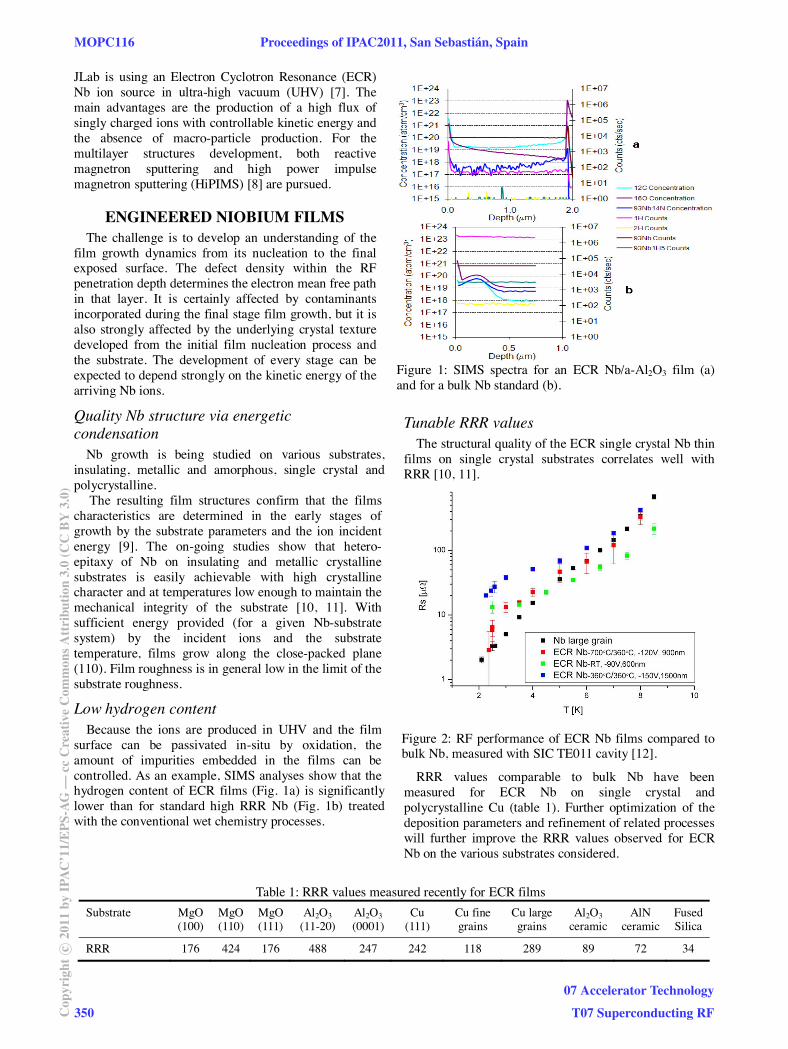
Tunable RRR values The structural quality of the ECR single crystal Nb thin
films on single crystal substrates correlates well with RRR [10, 11].
RRR values comparable to bulk Nb have been measured for ECR Nb on single crystal and polycrystalline Cu (table 1). Further optimization of the deposition parameters and refinement of related processes will further improve the RRR values observed for ECR Nb on the various substrates considered.
Table 1: RRR values measured recently for ECR films
Substrate MgO (100)
MgO (110)
MgO (111)
Al2O3 (11-20)
Al2O3 (0001)
Cu (111)
Cu fine grains
Cu large grains
Al2O3 ceramic
AlN ceramic
Fused Silica
RRR 176 424 176 488 247 242 118 289 89 72 34
Figure 1: SIMS spectra for an ECR Nb/a-Al2O3 film (a) and for a bulk Nb standard (b).
Figure 2: RF performance of ECR Nb films compared to bulk Nb, measured with SIC TE011 cavity [12].
MOPC116 Proceedings of IPAC2011, San Sebastián, Spain
350Cop
yrig
htc ○
2011
byIP
AC
’11/
EPS
-AG
—cc
Cre
ativ
eC
omm
onsA
ttri
butio
n3.
0(C
CB
Y3.
0)
07 Accelerator Technology
T07 Superconducting RF
RF measurements for corresponding disk samples are also in progress to determine the surface impedance and other parameters like the London penetration depth �. Fig. 2 shows the surface resistance behavior for ECR films coated at different bias voltages, baking and coating temperatures versus bulk Nb.
MULTILAYER FILMS The ternary nitride NbTiN presents all the advantages
of NbN and exhibits increased metallic electrical conduction properties with titanium (Ti) content. Ti is a good nitrogen getter, so the higher the Ti percentage, the lower the number of vacancies. In contrast with NbN, the B1-TiN phase is stable at room temperature. The two nitride phases are completely miscible resulting in a superconducting ternary NbTiN cubic phase thermodynamically stable at room temperature [13]. Tc is slightly higher for NbTiN but as for NbN, N stoichiometry is critical to obtaining the right superconducting phase. The properties (Tc) of NbTiN have been found to be enhanced by very thin insulating AlN films [14].
NbTiN/AlN/Nb structures
This study uses an UHV multi-technique deposition system tailored to in-situ multilayer depositions [15].
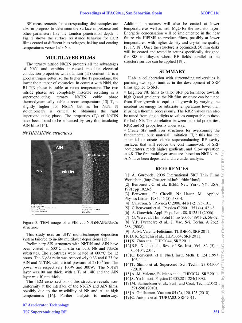
Preliminary SIS structures with NbTiN and AlN have been coated at 600°C in-situ on bulk Nb and Nb/Cu substrates. The substrates were heated at 600°C for 12 hours. The N2/Ar ratio was respectively 0.33 and 0.23 for AlN and NbTiN, with a total pressure of 2x10⁻³Torr. The power was respectively 100W and 300W. The NbTiN layer was100 nm thick, with a Tc of 14K and the AlN layer was 10 nm thick.
The TEM cross section of this structure reveals non-uniformity at the interface of the NbTiN and AlN films, possibly due to the miscibility of Nb and Al at high temperatures [16]. Further analysis is underway.
Additional structures will also be coated at lower temperature as well as with MgO for the insulator layer. Energetic condensation will be implemented in the near future via HiPIMS to produce films, possibly at lower temperatures, with higher density and crystalline quality [8, 17, 18]. Once the structure is optimized, 50 mm disks will be coated and tested in setups specifically designed for SIS multilayers where RF fields parallel to the structure surface can be applied [19].
SUMMARY JLab in collaboration with surrounding universities is
pursuing two opportunities in the development of SRF films applied to SRF. • Engineer Nb films to tailor SRF performance towards high Q and gradients: the Nb film structure can be tuned from fiber growth to equi-axial growth by varying the incident ion energy for substrate temperatures lower than if using a thermal process only. The RRR values can also be tuned from single digits to values comparable to those for bulk Nb. The correlation between material properties, RRR and RF properties is under way. • Create SIS multilayer structures for overcoming the fundamental bulk material limitation, Hc1: this has the potential to create viable superconducting RF cavity surfaces that will reduce the cost framework of SRF accelerators, reach higher gradients, and allow operation at 4K. The first multilayer structures based on NbTiN and AlN have been deposited and are under analysis.
REFERENCES [1] A. Gurevich, 2006 International SRF Thin Films Workshop, (http://master.lnl.infn.it/thinfilms/). [2] Benvenuti, C. et al., IEEE: New York, NY, USA, 1991; pp 1023-5. [3] Benvenuti, C.; Circelli, N.; Hauer, M., Applied Physics Letters 1984, 45 (5), 583-4. [4] Calatroni, S., Physica C 2006, 441(1-2), 95-101. [5] C.Benvenuti et al., Physica C 2001, 351 (4), 421-8. [6] A. Gurevich, Appl. Phys. Lett. 88, 012511 (2006). [7] G. Wu et al. Thin Solid Films 2005, 489(1-2), 56-62. [8] Y.P. Purandare et al., J. Vac. Sci. Techn. A 26(2) 288, (2008). [9] A.-M. Valente-Feliciano, TUIOB06, SRF 2011. [10] J. K. Spradlin et al., THPO064, SRF 2011. [11] X. Zhao et al. THPO044, SRF 2011. [12] B.P. Xiao et al., Rev. of Sc. Inst. Vol. 82 (5) p.
056104, 2011. [13] C. Benvenuti et al. Nucl. Instr. Meth. B 124 (1997)
106-111. [14] T. Shiino et al, Supercond. Sci. Techn. 23 045004
(2010). [15] A.-M. Valente-Feliciano et al., THPO074, SRF 2011. [16] S. Yoshimori, Physica C 305,281–284(1998). [17] M. Samuelsson et al., Surf. and Coat. Techn.205(2),
591-596 (2010). [18] A. Guillaumot, Vacuum 85 (2), 120-125 (2010). [19] C. Antoine et al. TUIOA03, SRF 2011.
Figure 3: TEM image of a FIB cut NbTiN/AlN/Nb/Cu structure.
Proceedings of IPAC2011, San Sebastián, Spain MOPC116
07 Accelerator Technology
T07 Superconducting RF 351 Cop
yrig
htc ○
2011
byIP
AC
’11/
EPS
-AG
—cc
Cre
ativ
eC
omm
onsA
ttri
butio
n3.
0(C
CB
Y3.
0)