development of parallel queue processor architecture...
TRANSCRIPT

A thesis submitted in partial satisfaction of the
requirements for the degree of
Master of Computer Science and Engineering
in the Graduate School of
the University of Aizu
Development of
Parallel Queue Processor Architecture
and its Integrated Development Environment
by
Hiroki Hoshino
February 2011
The thesis titled
Development ofParallel Queue Processor Architecture
and its Integrated Development Environment
by
Hiroki Hoshino
is reviewed and approved by:
Main referee
Assistant Professor Date
Ben Abdallah Abdrazek
Assistant Professor Date
Hiroshi Saito
Assistant Professor Date
Song Guo
The University of Aizu
February 2011
Contents
Chapter 1 Introduction 11.1 Background . . . . . . . . . . . . . . . . . . . . . . . . . . . . . . . 11.2 Related Works . . . . . . . . . . . . . . . . . . . . . . . . . . . . . . 21.3 Research Objective . . . . . . . . . . . . . . . . . . . . . . . . . . . 21.4 Thesis Organization . . . . . . . . . . . . . . . . . . . . . . . . . . . 3
Chapter 2 Queue Computation Model Overview 42.1 Produced Consumed Order Queue Computation Model . . . . . . . .62.2 Consumed Order Queue Computation Model . . . . . . . . . . . . . 72.3 Produced Order Queue Computation Model . . . . . . . . . . . . . . 7
Chapter 3 Produced Order Parallel Queue Processor Architecture 83.1 Instruction Set Architecture . . . . . . . . . . . . . . . . . . . . . .. 83.2 Processing Steps . . . . . . . . . . . . . . . . . . . . . . . . . . . . 9
3.2.1 Fetch Stage . . . . . . . . . . . . . . . . . . . . . . . . . . . 113.2.2 Decoding and Dynamic Operand Calculation Stage . . . . . .113.2.3 Queue Computation Stage . . . . . . . . . . . . . . . . . . . 123.2.4 Issue and Reservation Station Stage . . . . . . . . . . . . . . 123.2.5 Execution Stage . . . . . . . . . . . . . . . . . . . . . . . . 123.2.6 Queue Write Back Stage . . . . . . . . . . . . . . . . . . . . 12
3.3 Issue Algorithm . . . . . . . . . . . . . . . . . . . . . . . . . . . . . 133.3.1 Issue Logic . . . . . . . . . . . . . . . . . . . . . . . . . . . 133.3.2 Reservation Station Scheme . . . . . . . . . . . . . . . . . . 17
EX RS . . . . . . . . . . . . . . . . . . . . . . . . . . . . . 17SET RS . . . . . . . . . . . . . . . . . . . . . . . . . . . . . 17LDST RS . . . . . . . . . . . . . . . . . . . . . . . . . . . . 17BRANCH RS . . . . . . . . . . . . . . . . . . . . . . . . . . 19
3.4 Circular Queue Register Architecture . . . . . . . . . . . . . . . . .19
Chapter 4 Integrated Development Environment 214.1 Queue Compiler . . . . . . . . . . . . . . . . . . . . . . . . . . . . . 21
4.1.1 Characteristics . . . . . . . . . . . . . . . . . . . . . . . . . 214.1.2 Structure . . . . . . . . . . . . . . . . . . . . . . . . . . . . 22
4.2 Queue Assembler . . . . . . . . . . . . . . . . . . . . . . . . . . . . 234.2.1 Characteristics . . . . . . . . . . . . . . . . . . . . . . . . . 234.2.2 Structure . . . . . . . . . . . . . . . . . . . . . . . . . . . . 24
iii
4.3 Queue Simulator . . . . . . . . . . . . . . . . . . . . . . . . . . . . 24
Chapter 5 Design Result 275.1 Benchmark Analysis . . . . . . . . . . . . . . . . . . . . . . . . . . 275.2 Synthesis Result . . . . . . . . . . . . . . . . . . . . . . . . . . . . . 28
Chapter 6 Conclusion 31
Publication 32
References 33
Appendix A Queue Core 3 Verilog-HDL code 35
iv
List of Figures
Figure 2.1 Example of queue program generation . . . . . . . . . . .. . 4Figure 2.2 Example of queue computation steps . . . . . . . . . . . .. . 5Figure 2.3 DAG including problems of the queue computation model . . . 6Figure 2.4 DAG solving the problems with the produced consumed order
queue computation model . . . . . . . . . . . . . . . . . . . . . . . . 6Figure 2.5 DAG solving the problems with the consumed order and the
produced order queue computation model . . . . . . . . . . . . . . . 7
Figure 3.1 QC-3 instruction format and computation examples. . . . . . 9Figure 3.2 QC-3 system architecture . . . . . . . . . . . . . . . . . . . . 10Figure 3.3 Pipeline stage example . . . . . . . . . . . . . . . . . . . . . 11Figure 3.4 Instruction allocation module. The instructionis distributed
according to the information generated by this. . . . . . . . . . .. . 13Figure 3.5 Instruction allocation information generationalgorithm. This
chart is repeated four times. . . . . . . . . . . . . . . . . . . . . . . . 15Figure 3.6 Tag generation algorithm. The initialization step is run once at
one cycle and generation chart is repeated four times. . . . . .. . . . 16Figure 3.7 The SET RS tag matching scheme . . . . . . . . . . . . . . . 18Figure 3.8 The LDST RS tag matching scheme . . . . . . . . . . . . . . 19Figure 3.9 The circular queue register (QREG) structure . . . .. . . . . 19
Figure 4.1 Queue Compiler structure . . . . . . . . . . . . . . . . . . . . 22Figure 4.2 Queue Assembler structure . . . . . . . . . . . . . . . . . . .23Figure 4.3 Top view of the Queue Simulator . . . . . . . . . . . . . . . .25Figure 4.4 Simulation result: The intermediate QREG contentis shown in
middle, Simulator behavior is shown in right . . . . . . . . . . . . .. 26
Figure 5.1 Altera Stratix III development board . . . . . . . . . .. . . . 29Figure 5.2 The actual power consumption on Altera Stratix III develop-
ment board (mW) . . . . . . . . . . . . . . . . . . . . . . . . . . . . 30
v

List of Tables
Table 5.1 Benchmark analysis . . . . . . . . . . . . . . . . . . . . . . . 27Table 5.2 Simulation Result . . . . . . . . . . . . . . . . . . . . . . . . . 28Table 5.3 The number of Logic Elements (LEs). Target device:Stratix,
EP1S80F1020C5) . . . . . . . . . . . . . . . . . . . . . . . . . . . . 28Table 5.4 Synthesis result of QC-3. Target device: Stratix III, EP3SL150F1152C2 29
vi

Acknowledgement
I wish to express my appreciation to Dr. Ben A. Abdrazek for hisexcellent adviceand diligent efforts to guide me through this project. And hegave me good opportuni-ties to improve my skills, which are a way of study and English. Also I would like toappreciate to Dr. Hiroshi Saito and Dr. Song Guo of University of Aizu to revise mythesis. Moreover Dr. Kenichi Kuroda, Dr. Yuichi Okuyama, and Dr. Junji Kitamichihelped my troubles and problems about my project.
Finally, I am deeply grateful to the members of the Adaptive Systems Laboratoryat the University of Aizu. These people have supported not only researches but alsomy school life. I could not have marvelous days in the University of Aizu without a lotof great friends.
vii

Abstract
The high performance processors have been required long time. The instructionlevel parallelism (ILP) is one of the important essences to enable processors to be highperformance processors. There are two main techniques to exploit ILP, VLIW andsuperscalar. The complex compiler to generate the VLIW instruction is needed in theaspect of software. The superscalar scheme needs large areafor the finding ILP withbig instruction window and register renaming techniques.
The queue instruction set processor architecture is the approach to get ILP withsimple techniques. The intermediate results are saved in the queue register, whichfollows the first-in first-out rule, instead of the random access register. The instructionreads the operand from the head of the queue register implicitly. The execution resultis written into the tail of the queue implicitly. There is no need to specify the registernumber in the instructions. The instructions for the queue processor are generated bytraversing the data acyclic graph in level order manner. There are promising advantagesin the queue processor; high ILP and short instruction width.
In this thesis, the superscalar, out-of-order, produced order parallel queue processor(QC-3) is designed. The design is implemented by Verilog-HDLto get high accurateevaluation result with synthesis tools provided by a company. And also the queuecompiler, the assembler and its simulator are proposed. These design suites are usefulto design the programs for the queue processor.

Chapter 1
Introduction
1.1 Background
The high performance processors have been required long time. The instructionlevel parallelism (ILP) is one of the important essences to enable processors to be highperformance processors. The higher parallelism the program has, the more instructionsare executed in parallel. Then the execution time is shorter. To extract ILP, the com-pilers calculate the relationship among the program whether there are any independentinstructions and arrange the register number and the instruction order. Also the ex-isting processors run many in-flight instructions with dynamic scheduling scheme andregister renaming. The compilers are very complex in order to deal with the registerpressure program and parallelism extracting problem. The processors need more areaof the scheduling scheme and register renaming [1]. They arevery complex and thebigger area consumes more power.
Existing processors have implemented the instruction window, the register renam-ing scheme [2] and the reservation stations to exploit ILP. The MIPS R10000 [3] hasthe register renaming schemes which are free list, active list, and register map table.Also there are 16-entry instruction queues to extruct ILP. The PowerPC 750 [4] hasa 6-entry issue queue and dispatches up to 2 instructions in the bottom of the queue.Each functional unit has a reservation station to wait for the availability of all operanddata. The Alpha 21246 [5] has two register renaming schemes and two issue queues toextruct ILP. The UltraSparc I [6] has the renaming scheme andthe instruction bufferwhich has 12 entries to extruct ILP. Also the re-order bufferto realize out-of-orderscheme is implemented in these processors.
The keys are simple and fast execution time to get high performance processors.The queue computation model is an approach to get the keys, which is originated by theideas in [7][8]. The most important idea of this computationis the mechanism of theregister handling which holds the intermediate calculation results. In the queue com-putation model, an instruction uses the First-in First-Outregister, which is so calledqueue, instead of the random access register as the storage of the intermediate results.The instructions remove the required data from the head of the operand queue andinsert the result at the tail of the operand queue.
The queue computation model needs only the operation code. The source is takenimplicitly from the queue entry pointed by the queue head pointer. The result is in-
1

serted into the queue tail pointer implicitly. There is no need to specify the operandregister number in the instruction. All we have to do is just specifying the operationcode. The instructions do not specify any operands and destination address. Thisadvantage causes the program size smaller. Also there is no false data dependency be-cause the register number is not specified in the compile time. Thus there is no registerrenaming scheme in hardware.
1.2 Related Works
The QC-2 was proposed in [9][10][11][12], which employs the produced orderqueue computation model. In the produced order queue model,the first source operandis always read from the head of the queue register and the second source operand isread from the position addressed with an offset from the queue head. The instructionsare generated by level-order manner which traverse the dataflow graph from upperleft to lower right [7][13][14][15]. In this traversal, thenodes in the same layer arenot dependent. Thus there are executed in parallel. This characteristic enables thecompiler and the processor to extract ILP easily. The advantages of QC-2 are highinstruction level parallelism and short cord size.
1.3 Research Objective
In this paper, the superscalar, out-of-order, produced order parallel queue processor(QC-3) is designed. And also the queue compiler, the assembler and its simulator areanalysed. These design suites are useful to design the program for the queue processor.The independent instructions are found in the superscalar processor with the issue logic[16]. This issue logic is complex and many papers are lookingfor the efficient issuedesign including the superscalar processor design [17][18][19]. In the queue processor,the program has the natural ILP. So the complex issue logic isnot needed. Moreoverthe instruction window, which extracts ILP in general processors, is small in the queueprocessor. Also the survey of the queue processor characteristics [20][8] mentions thatwhen every functional unit, such as EX unit and LDST unit, has9 execution unitswith 15-instruction fetch width, the most parallelism is exploited, assuming that eachexecution unit can execute in the same cycle. Also in small number of execution units,the out-of-order scheme runs efficiently. Adapting the out-of-order scheme enables thequeue processor to get more efficient calculation and to support the functional unitshaving different execution cycle.
In the previous prototype design QC-2, the in-order scheme isemployed. The QC-2 is assumed that the needed execution cycles in the functional unit are the same. Forexample, the addition, division and multiply execution instructions take single cycle inexecution stage. Generally the division and the floating point execution need a lot ofcycles to accomplish high clock frequency. If the multi-cycle execution units are imple-mented, the in-order scheme does not run efficiently. The following instructions needto wait the completion of the previous instruction which uses a multi-cycle functionalunit. Thus the QC-3 employs the out-of-order scheme. The out-of-order program exe-cution needs a re-order buffer to keep in-order program completion correctly. However
2
the instructions for the QC-3 are not specified the register number at compile time. Theregister number is assigned at run-time in program order using the head pointer of thequeue register and the tail pointer of the queue. Thus an instruction for the QC-3 com-plete anytime, which means out-of-order completion can be adapted. The QC-3 canexecute instructions in an out of the program order with multiple functional units withnew issue logic and reservation station.
There are 4 arithmetic execution units, 4 set register units, 1 load store unit, 1branch / control unit in the QC-3. The number of functional units is same as the QC-2because it is easy to compare new one with previous one. Each unit has reservationstations, which holds the instruction until all operand available. To distribute the in-struction to the proper reservation station, the issue unitis developed with simple tagmatching. The QC-3 is implemented by HDL to make the evaluation easy and ac-curate. The QC-3 is synthesized for the Stratix III FPGA device by the Quartus IIsoftware, which both are provided by Altera inc.. This design approach results in moreaccurate speed, area and power consumption evaluation.
1.4 Thesis Organization
The rest of this paper describes as follows: Capter 2 reviews the Queue Compu-tation Models. In Chapter 3, the QC-3 processor architecture is mentioned. Chapter4 gives the Integrated Development Environment, which are The Queue Compiler,Queue Assembler and Queue Simulator. In Chapter 5, the designresults of QC-3 isdescribed. Last chapter mentions the conclusion.
3
Chapter 2
Queue Computation Model Overview
The queue computation model uses the queue data structures for operands manip-ulation. In this model, the source operand is read from the queue head (QH) and resultis written into the queue tail (QT). The instrucions do not specify the address explicitlybecause the addresses of the source operands and destination are defined implicitly.There are advantages of this computation model. No specifying operand derives theshorter instruction width. Thus the program size is small. Also the register addressesare computed at the run-time. Thus there are no false data dependency. Moreoverthe program of the queue computation model has a high instruction level paralellism(ILP). The program of queue computation model is generated by traversing the leve-order manner. The reason why it has a high parallelism is thatthe same level nodes areindependent each other.
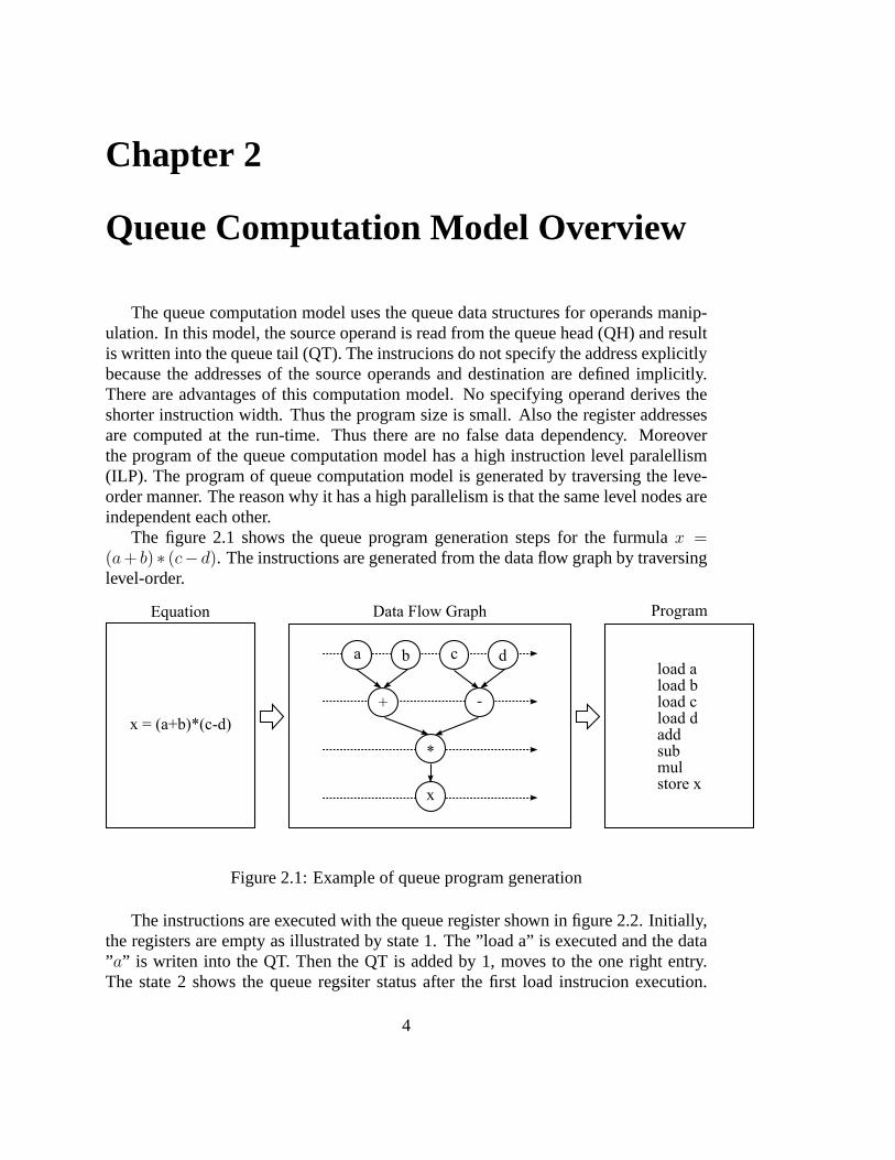
The figure 2.1 shows the queue program generation steps for the furmulax =(a+ b) ∗ (c− d). The instructions are generated from the data flow graph by traversinglevel-order.
Equation
x = (a+b)*(c-d)
a b c d
+ -
*
x
Data Flow Graph
load aload bload cload daddsubmulstore x
Program
Figure 2.1: Example of queue program generation
The instructions are executed with the queue register shownin figure 2.2. Initially,the registers are empty as illustrated by state 1. The ”load a” is executed and the data”a” is writen into the QT. Then the QT is added by 1, moves to the one right entry.The state 2 shows the queue regsiter status after the first load instrucion execution.
4
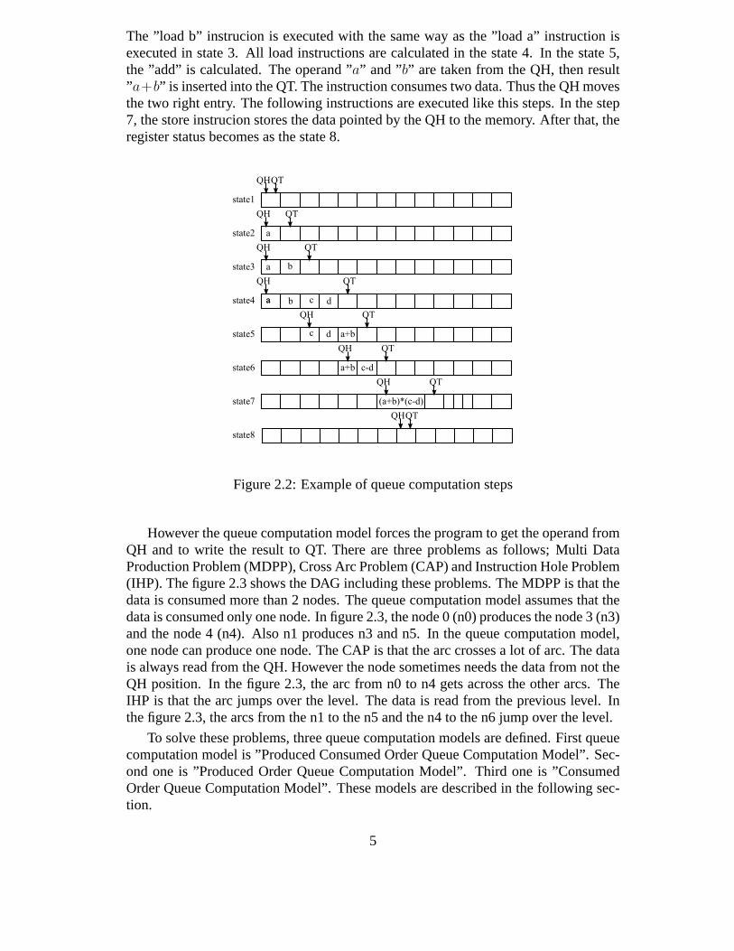
The ”load b” instrucion is executed with the same way as the ”load a” instruction isexecuted in state 3. All load instructions are calculated inthe state 4. In the state 5,the ”add” is calculated. The operand ”a” and ”b” are taken from the QH, then result”a+b” is inserted into the QT. The instruction consumes two data.Thus the QH movesthe two right entry. The following instructions are executed like this steps. In the step7, the store instrucion stores the data pointed by the QH to the memory. After that, theregister status becomes as the state 8.
Figure 2.2: Example of queue computation steps
However the queue computation model forces the program to get the operand fromQH and to write the result to QT. There are three problems as follows; Multi DataProduction Problem (MDPP), Cross Arc Problem (CAP) and Instruction Hole Problem(IHP). The figure 2.3 shows the DAG including these problems.The MDPP is that thedata is consumed more than 2 nodes. The queue computation model assumes that thedata is consumed only one node. In figure 2.3, the node 0 (n0) produces the node 3 (n3)and the node 4 (n4). Also n1 produces n3 and n5. In the queue computation model,one node can produce one node. The CAP is that the arc crosses a lot of arc. The datais always read from the QH. However the node sometimes needs the data from not theQH position. In the figure 2.3, the arc from n0 to n4 gets acrossthe other arcs. TheIHP is that the arc jumps over the level. The data is read from the previous level. Inthe figure 2.3, the arcs from the n1 to the n5 and the n4 to the n6 jump over the level.
To solve these problems, three queue computation models aredefined. First queuecomputation model is ”Produced Consumed Order Queue Computation Model”. Sec-ond one is ”Produced Order Queue Computation Model”. Third one is ”ConsumedOrder Queue Computation Model”. These models are described in the following sec-tion.
5

a b c
+ -
*
x
*
n0 n1 n2
n3 n4
n5
n6
n7
Figure 2.3: DAG including problems of the queue computationmodel
2.1 Produced Consumed Order Queue Computation Model
The produced consumed order queue computation model is a normal model follow-ing the FIFO rule. The data is always read from the QH. The result is always writteninto the QT. The restriction is very strong. In this model, tosolve the three problems,many instructions are inserted. The number of the load instrucion is increased for solv-ing the MDPP by the number of the production nodes. To solve the CAP, the node isspilled out in the memory and refilled at an approapriate timeusing the load and storeinstructions. Also to solve the CAP, the ”dup” instructions that can copy the data inthe QH to the QT are inserted into every places jumping the level. The DAG solvingthe problems is in the figure 2.4. However these solutions make its program biggerobviously.
a b c
+
-
*
x
*
n0 n1 n2
n3
n4
n5
n6
n7
a b
dup
st
ld
dup
dup dup
Figure 2.4: DAG solving the problems with the produced consumed order queue com-putation model
6

2.2 Consumed Order Queue Computation Model
In the consumed order queue computation mode, the first source data is always readfrom the QH and second souce data is read from the next QH. And the result is writteninto the QT and the place pointed by sum of the QT and the specified offset. Thereforethis model can produce two data with one instruction. In the figure 2.5 a), the n0 is theload instruction. This load instruction specify the offsetin 2, like a ”load a 2”. Sincethe data ”a” is inserted into the QT andQT + 2, the n4 calculates completely with theFIFO rule. In this solution, upper two data is generated in one instrucion and anotherone is inserted into the place away from the QT with specifying offset. However tosolve the MDPP, many load instructions are still needed. Also the instruction width iswider so that the operand is specified. Thus the probram size is bigger.
2.3 Produced Order Queue Computation Model
In the produced order queue computation model, the first source data is read fromthe QH. And the second source data is read from the place pointed by sum of the QHand the specified offset. Then the calculation result is always written into the QT. Theused data can be used again. If the data is not used anymore, the data is removedfrom the queue register. In the figure 2.5 b), the n4 is sub instruction, which have aoffset like a ”subo -2”. The deference between ”sub” and ”subo” is the first and secondoperands are in an opposite side. The first operand data is taken from the place pointedby theQH − 2 position where it is in the n0. The second operand data is taken fromthe QH where it is in the n2. And the result is written into the QT. In this solusion, theinstructions can use the data again. The efficient usage of the queue register is achived.All of the problems explained above are solved in this model.And the best modelof the queue processor is this produced order queue computation model in the paper[21][22].
a b c
+ -
*
x
*
n0 n1 n2
n3n4
n5
n6
n7
a
b
a b c
+ -
*
x
*
n0 n1 n2
n3 n4
n5
n6
n7
a) Consumed order QCM b) Produced order QCM
Figure 2.5: DAG solving the problems with the consumed orderand the producedorder queue computation model
7
Chapter 3
Produced Order Parallel QueueProcessor Architecture
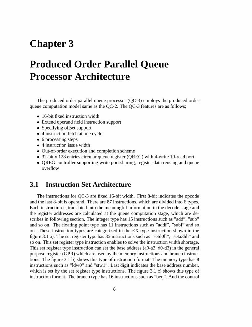
The produced order parallel queue processor (QC-3) employs the produced orderqueue computation model same as the QC-2. The QC-3 features areas follows;
• 16-bit fixed instruction width• Extend operand field instruction support• Specifying offset support• 4 instruction fetch at one cycle• 6 processing steps• 4 instruction issue width• Out-of-order execution and completion scheme• 32-bit x 128 entries circular queue register (QREG) with 4-write 10-read port• QREG controller supporting write port sharing, register data reusing and queue
overflow
3.1 Instruction Set Architecture
The instructions for QC-3 are fixed 16-bit width. First 8-bit indicates the opcodeand the last 8-bit is operand. There are 87 instructions, which are divided into 6 types.Each instruction is translated into the meaningful information in the decode stage andthe register addresses are calculated at the queue computation stage, which are de-scribes in following section. The integer type has 15 instructions such as ”add”, ”sub”and so on. The floating point type has 11 instructions such as ”addf”, ”subf” and soon. These instruction types are categorized in the EX type instruction shown in thefigure 3.1 a). The set register type has 35 instructions such as ”setd0ll”, ”seta3hh” andso on. This set register type instruction enables to solve the instruction width shortage.This set register type instruction can set the base address (a0-a3, d0-d3) in the generalpurpose register (GPR) which are used by the memory instructions and branch instruc-tions. The figure 3.1 b) shows this type of instruction format. The memory type has 8instructions such as ”ldw0” and ”stw1”. Last digit indicates the base address number,which is set by the set register type instructions. The figure3.1 c) shows this type ofinstruction format. The branch type has 16 instructions such as ”beq”. And the control
8
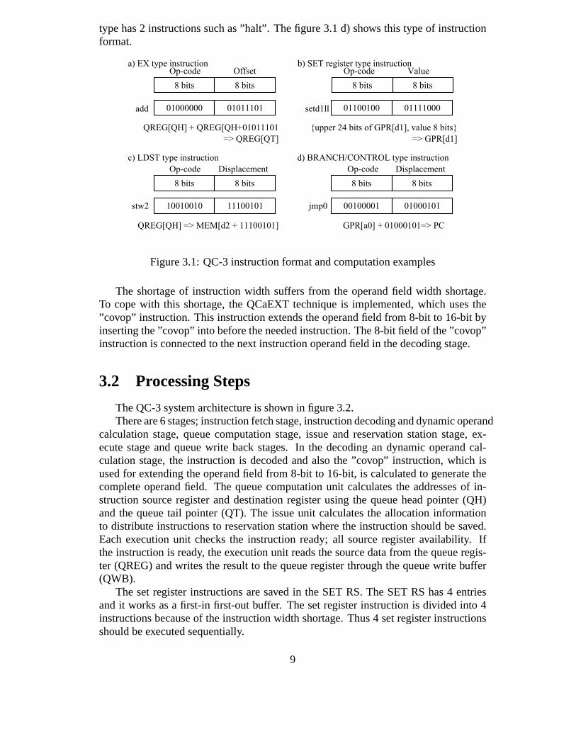
type has 2 instructions such as ”halt”. The figure 3.1 d) showsthis type of instructionformat.
8 bits 8 bits
01000000 01011101
8 bits 8 bits
8 bits 8 bits
8 bits 8 bits
Op-code Offset Op-code Value
Op-code Displacement Op-code Displacement
c) LDST type instruction
a) EX type instruction b) SET register type instruction
d) BRANCH/CONTROL type instruction
01100100 01111000
00100001 0100010110010010 11100101
add setd1ll
jmp0stw2
QREG[QH] + QREG[QH+01011101
=> QREG[QT]
{upper 24 bits of GPR[d1], value 8 bits}
=> GPR[d1]
QREG[QH] => MEM[d2 + 11100101] GPR[a0] + 01000101=> PC
Figure 3.1: QC-3 instruction format and computation examples
The shortage of instruction width suffers from the operand field width shortage.To cope with this shortage, the QCaEXT technique is implemented, which uses the”covop” instruction. This instruction extends the operandfield from 8-bit to 16-bit byinserting the ”covop” into before the needed instruction. The 8-bit field of the ”covop”instruction is connected to the next instruction operand field in the decoding stage.
3.2 Processing Steps
The QC-3 system architecture is shown in figure 3.2.There are 6 stages; instruction fetch stage, instruction decoding and dynamic operand
calculation stage, queue computation stage, issue and reservation station stage, ex-ecute stage and queue write back stages. In the decoding an dynamic operand cal-culation stage, the instruction is decoded and also the ”covop” instruction, which isused for extending the operand field from 8-bit to 16-bit, is calculated to generate thecomplete operand field. The queue computation unit calculates the addresses of in-struction source register and destination register using the queue head pointer (QH)and the queue tail pointer (QT). The issue unit calculates the allocation informationto distribute instructions to reservation station where the instruction should be saved.Each execution unit checks the instruction ready; all source register availability. Ifthe instruction is ready, the execution unit reads the source data from the queue regis-ter (QREG) and writes the result to the queue register throughthe queue write buffer(QWB).
The set register instructions are saved in the SET RS. The SET RShas 4 entriesand it works as a first-in first-out buffer. The set register instruction is divided into 4instructions because of the instruction width shortage. Thus 4 set register instructionsshould be executed sequentially.
9

Fetch Unit
Queue Computation Unit
Decode Unit
Issue Unit
EX
Inst Mem
Data Mem
LDST EXBR EX
EX EXEX
RS RS RS RS RS RS
QWB QREG
SET SET
RS RS
GPR
SET SET
RS RS
Figure
3.2:Q
C-3
systemarchitecture
10
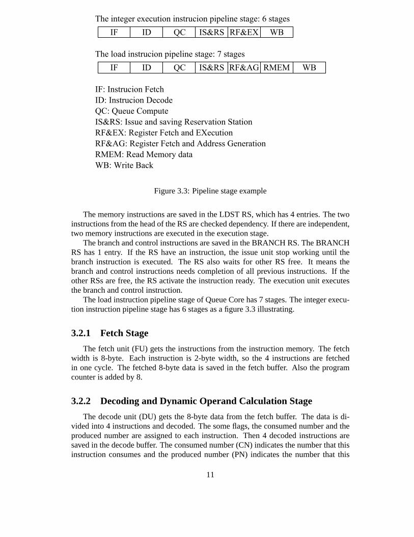
QCIDIF IS&RS RF&EX WB
QCIDIF IS&RS RF&AG WBRMEM
The integer execution instrucion pipeline stage: 6 stages
The load instrucion pipeline stage: 7 stages
IF: Instrucion Fetch
ID: Instrucion Decode
QC: Queue Compute
IS&RS: Issue and saving Reservation Station
RF&AG: Register Fetch and Address Generation
RF&EX: Register Fetch and EXecution
RMEM: Read Memory data
WB: Write Back
Figure 3.3: Pipeline stage example
The memory instructions are saved in the LDST RS, which has 4 entries. The twoinstructions from the head of the RS are checked dependency. If there are independent,two memory instructions are executed in the execution stage.
The branch and control instructions are saved in the BRANCH RS. The BRANCHRS has 1 entry. If the RS have an instruction, the issue unit stopworking until thebranch instruction is executed. The RS also waits for other RS free. It means thebranch and control instructions needs completion of all previous instructions. If theother RSs are free, the RS activate the instruction ready. The execution unit executesthe branch and control instruction.
The load instruction pipeline stage of Queue Core has 7 stages. The integer execu-tion instruction pipeline stage has 6 stages as a figure 3.3 illustrating.
3.2.1 Fetch Stage
The fetch unit (FU) gets the instructions from the instruction memory. The fetchwidth is 8-byte. Each instruction is 2-byte width, so the 4 instructions are fetchedin one cycle. The fetched 8-byte data is saved in the fetch buffer. Also the programcounter is added by 8.
3.2.2 Decoding and Dynamic Operand Calculation Stage
The decode unit (DU) gets the 8-byte data from the fetch buffer. The data is di-vided into 4 instructions and decoded. The some flags, the consumed number and theproduced number are assigned to each instruction. Then 4 decoded instructions aresaved in the decode buffer. The consumed number (CN) indicates the number that thisinstruction consumes and the produced number (PN) indicates the number that this
11

instruction produces, which are used by next unit, the queuecomputation unit. Alsothe ”covop” instruction is calculated in this stage. The covop register is implementedto hold the operand data and concatenate the next instruction operand field with thecovop operand filed data.
3.2.3 Queue Computation Stage
The queue computation unit (QCU) computes the addresses of source and destina-tion. This unit is one of the key units of the queue processor.The register numbers arecalculated dynamically. This unit holds the head pointer ofthe queue register, which iscalled QH, and the tail pointer of the queue register, which is called QT. Also this unitholds the live queue pointer, which enables to reuse the datain QREG, called LQH. Thefirst source address is decided by the QH, and second source address is decided by thesum of the QH and the offset that its instruction has. Also thedestination address is de-cided by the QT. After that the pointers are increased with following formula. The nextQH is calculated by the formula,QHnext = QHcurrent+consumednumber(CN). Thenext QT is calculated by the formula,QTnext = QTcurrent + producednumber(PN).LQH is basically same as QH. If the STOP LQH instruction, which is named ”stplqh”,comes into the QCU, QH current is held by LQH until the AUTO LQH instructioncomes. If the AUTO LQH instruction, which is named ”autlqh”,comes to the QCU,LQH pointer moves automatically from the LQH value plus offset position. The 4 in-structions which have calculated addresses are inserted into the instruction queue (IQ)which holds the executive instructions. The instruction queue has 8-entry buffer. TheIQ can send up to 4 instructions depending on the issue stage availability. If the IQ isfull, previous units are stalling until the IQ is not full.
3.2.4 Issue and Reservation Station Stage
The issue unit (IU) has the issue logic and the reservation stations (RSs). The issuelogic checks the RS availability and makes the allocation information for 4 instruc-tions from the IQ. Each instruction is distributed into appropriate RS depending on itsinstruction type. This issue mechanism is described later.
3.2.5 Execution Stage
There are 4 EX, 4 SET, 1 LDST and 1 BRANCH units. The EX unit includesthe execution function of integer and floating point. The ready instruction is fed fromeach RS and executes each execution modules. When the execution module finishescalculating the instruction, the module sends the finish signal to the RS which releasesthe RS slot.
3.2.6 Queue Write Back Stage
The results generated by each EX unit and LDST unit are written into the queuewrite buffer (QWB). The number of write port of the QREG is restricted to 4. TheQWB and QREG controller are implemented to share and arbitratethe QREG port.
12

The load data from the memory has a high priority. When the QWB has the data fromthe data memory, the data is written into the QREG first.
3.3 Issue Algorithm
In the in-order scheme, if there is an instruction which takes a long time to execute,the next instruction needs to wait for previous instructioncompletion. The previousQC-2 system assumes that every functional unit is executed inone cycle even if thefunctional unit handles the floating point execution. The survey of the queue processorcharacteristics [20] mentions that when the every functional unit, such as EX unit andLDST unit, have 8 execution units with 12-instruction fetchwidth, the most parallelismis exploited, assuming that each execution unit can executein the same cycle. Also insmall number of execution units, the out-of-order scheme runs efficiently. Adaptingthe out-of-order scheme enable the queue processor to get more efficient calculationand to support the functional units having different execution cycle.
The issue unit distributes the coming 4 instructions to eachreservation station.There are 1 slot RS for each EX unit, 4 slots RS for each SET unit, 4slots RS forLDST and 1 slot RS for BRANCH as illustrated by figure 3.2.
3.3.1 Issue Logic
RS_TYPE SRC0_adrs SRC1_adrs DEST_adrs EXE_FLAG PC
EX#_RS_free_table
SET#_RS_free_table
LDST_RS_free_table
BRAN_RS_free_table
IU_STALL
INST_VLD
SET_TAG
LDST_TAG
INST_GRANT
INST_RS#
INST_WP#
INST_TAG
INSTRUCTIONALLOCATIONMODULE
EX#_RS_free_table_updated
SET#_RS_free_table_updated
LDST_RS_free_table_updated
BRAN_RS_free_table_updated
IU_STALL_updated
SET_TAG_updated
LDST_TAG_updated
INST
3
1
1
2x4
4
1x4
4x4
4x1
1x1
4
3
2
7
1
2x4
4
1x4
4x4
4x1
1x1
2
EX_ALLOC
SET_ALLOC
LDST_ALLOC
BRAN_ALLOC
Figure 3.4: Instruction allocation module. The instruction is distributed according tothe information generated by this.
13

An instruction has the RS type information and the destination address. And theall RS have a free table which indicates whether the RS has any free RS slot or not.Also the tag register is in the issue module. Since the queue instruction set is fixed16-bit width, the operand field is 8-bit width. This instruction width is short to have anenough immediate value and memory displacement offset. Theaddress-register anddata-register are implemented in the QC-3. These registers are base register, whichenable instructions to access the full 32-bit memory space.And the set register in-structions are implemented in the queue processor to set these base registers. Howeverthe set register instructions and the memory access instructions are executed com-pletely in program order. For example when the load instruction using the d0 registeris executed before executing the set d0 register instruction, the load instruction refersan incorrect address. Thus the tag matching system is adapted to keep program order.After executing all previous set register instructions, the memory access instructionsare executed. Also after all previous memory access instructions are executed, the setregister instructions are executed. The tag field for set instruction is 2-bit. The tag fieldfor memory access instruction is 2-bit. And the destinationof lower 2-bit is needed.If the all previous set or memory instructions are executed,the issue module sets theinstruction ready bit to its instruction. If the instruction ready bit of a RS slot is set by1, the RS can send this slot instruction to the execution stagewithout checking the tag.The tag field is total 7-bit. The block diagram of this allocation module is shown infigure 3.4. And the allocation information algorithm is shown in figure 3.5. Also thetag information generation algorithm is shown in figure 3.6.
14

Figure 3.5: Instruction allocation information generation algorithm. This chart is re-peated four times. 15

Figure 3.6: Tag generation algorithm. The initialization step is run once at one cycleand generation chart is repeated four times.16
After an instruction is assigned the allocation information, the free tables of RS andthe tags are updated. This updated information is used for next following instructions.The issue logic calculates the allocation information for up to 4 instructions at onecycle. If any RS is full, the issue logic stop assigning allocation and updating RS freetables and tags. Also when the branch and control instructions are allocated into thebranch RS, the following instructions are stall to keep correctness.
3.3.2 Reservation Station Scheme
There are 4 types of reservation station. The RS holds the instruction(s) and sendsthe ready instruction(s) to execute.
EX RS
The EX RS has 1 slot to hold the execution type instructions. There are 4 EXRSs for 4 EX units. The RS checks the operand source registers availability using thequeue register ready bit (QREGRDY). If all QREGRDY addressed by source fields areset 1, the instruction can be executed. The RS sends this instruction to execution unitwith the instruction ready signal. When the instruction completes to be executed inthe execution stage, the execution unit sends the finish signal. The RS gets the finishsignal and releases the RS slot free with being set the free table by 0.
SET RS
The SET RS has 4 slots to hold the set register type instructions. There are 4 SETRSs for 4 SET units. The RS employs the queue scheme. The instruction of the head ofthe RS is sent to the execution stage. The RS slot has two bits to indicate the instructionvalid and ready. The instruction valid bit is set when the instruction is registered intothe slot. The ready is set if the tag sent from the LDST unit is matched with the tagthat the slot has. If the valid and ready are set, the instruction of the slot is send to theexecution unit. When the instruction completes to be executed in the execution stage,the execution unit sends the finish signal. The RS gets the finish signal and releasesthe RS slot free with being set the free table by 0.
The tag matching scheme is illustrated in figure 3.7. There are comparators tocheck the tag is matched or not. If it is matched, the tag readybit is set and theinstruction becomes ready to execute.
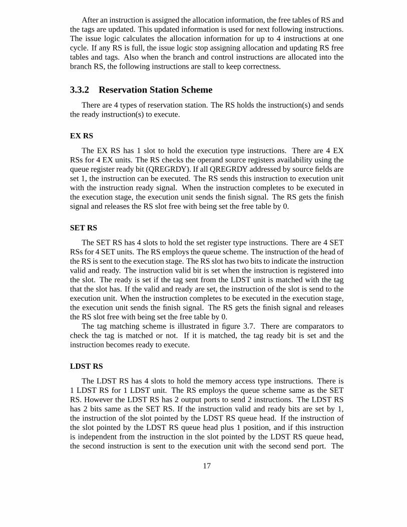
LDST RS
The LDST RS has 4 slots to hold the memory access type instructions. There is1 LDST RS for 1 LDST unit. The RS employs the queue scheme same as the SETRS. However the LDST RS has 2 output ports to send 2 instructions. The LDST RShas 2 bits same as the SET RS. If the instruction valid and readybits are set by 1,the instruction of the slot pointed by the LDST RS queue head. If the instruction ofthe slot pointed by the LDST RS queue head plus 1 position, and if this instructionis independent from the instruction in the slot pointed by the LDST RS queue head,the second instruction is sent to the execution unit with thesecond send port. The
17

V R LDST TAG INST.
E0
E1
E2
E3
SET0 RS
=
=
=
=
V R LDST TAG INST.
E0
E1
E2
E3
SET1 RS
=
=
=
=
V R LDST TAG INST.
E0
E1
E2
E3
SET2 RS
=
=
=
=
V R LDST TAG INST.
E0
E1
E2
E3
SET3 RS
=
=
=
=
LDST_TAG of
Finished LDST instruction
From LDST Unit 0From LDST Unit 1
Figure 3.7: The SET RS tag matching scheme
dependency is checked by the base register number, the offset, and op-code of both in-structions. There is no dependency in case of two load instructions. Otherwise in caseof either the op-codes are two store or load and store instruction series, the register andoffset are compared. If these are the same, these instructions are dependent. And aninstruction is set to the execution unit. When the instruction completes to be executedin the execution stage, the execution unit sends the finish signal. The RS gets the finishsignal and releases the RS slot free with being set the free table by 0.
The tag matching scheme is illustrated in figure 3.8. There are comparators tocheck the tag is matched or not. If it is matched, the tag readybit is set and theinstruction becomes ready to execute.
18
=
=
=
=
=
=
=
=
=
=
=
=
V R SET TAG INST.
E0
E1
E2
E3
LDST RS
=
=
=
=
SET TAG of
finished SET instructions
from SET UNIT 0from SET UNIT 1from SET UNIT 2from SET UNIT 3
Figure 3.8: The LDST RS tag matching scheme
BRANCH RS
The BRANCH RS has 1 slot to hold the branch and control type instructions. TheRS checks the other RS free table to recognize the all other previous instructions havebeen executed. If the other RSs are free, the RS sends the instruction to the executionunit. When the instruction completes to be executed in the execution stage, the execu-tion unit sends the finish signal. The RS gets the finish signal and releases the RS slotfree with being set the free table by 0.
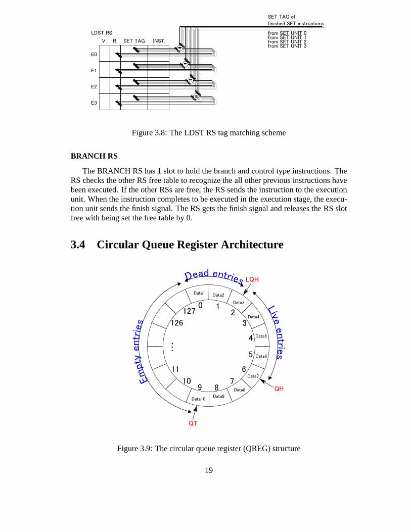
3.4 Circular Queue Register Architecture
0 12
3
4
5
6
789
10
11
126
127
LQH
QH
QT
Data1Data2
Data3
Data4
Data5
Data6
Data7
Data8
Data9Data10
Dead entries
Liv
e e
ntrie
s
Em
pty
entr
ies
.
.
.
Figure 3.9: The circular queue register (QREG) structure
19

The key units of the QC are this circular queue register (QREG)and its controller.The QREG has 3 pointers: LQH, QH and QT. The data is written intothe entry pointedby the QT. After the write back to the QREG, the QT is added by 1. The data is readfrom the entry pointed by the QH. After the read operand, the QH is added by 1. TheLQH is special pointer to use the data again. To control the LQH, there are ”stplqh”and ”autlqh” instructions. If the entry is used again, before the data is consumed, the”stplqh” instruction is executed to stop the LQH pointer. When the data is not used anymore, the ”autlqh” pointer is moves automatically. The QREG is divided into 3 typesof entries: empty entries, live entries and dead entries in figure 3.9
The QREG provides the operand data to 4 EX unit and 1 LDST unit. The numberof read port needs 10 and the number of write port needs 6. The more the numberof port increases, the more area is needed. So 6 write ports decreases into 4 writeports. The 2 write port is shared by 2 EX and LDST write port. The queue write buffer(QWB) is implemented to wait for arbitrating the write port sharing.
The QREG controller has the queue register ready bits (QREGRDY). When thedata is inserted into the QREG, the QREGRDY is set by 1. This bit indicates theavailability of QREG data to solve the true data dependency. When the data is read byinstruction, the QREGRDY is set by 0. The data of this entry is not available any more.If the ”stplqh” has been executed, the QREGRDY is not reset evenif the instructionconsumes the data from the QREG. When the ”autlqh” is executed,the QREGRDY isset by 0.
20

Chapter 4
Integrated Development Environment
There are design suites of the development queue program, which are the queuecompiler, the queue assembler and queue simulator. The queue compiler translates theassembly code from the high level language with gnu compilertool set. The queueassembler translates the machine code from the assembly code. The queue simulatorshows the behavior of the inside of the Queue Processor. These are analyzed in thischapter.
4.1 Queue Compiler
The Queue Compiler translates high level languages to the assembly codes. Thesome code optimizations are taken for shorter execution time program, higher paral-lelism, better resource utilization and amang others. The Cprograms are converted tothe assembly program for the Queue Processor using the GCC front-end, middle-endand Queue Related back-end. The queue compiler tasks are mainly three: (1) con-strain all instructions to have at most one offset reference, (2) compute offset referencevalues and (3) schedule the program expressions in level-order manner. This compilercan generate denser code comparing with the compilers for the RISC machine.
4.1.1 Characteristics
Generally, the compilers try to find the instruction level parallelism (ILP) in com-pile time. The register machine executes the instruction which has three operands,which are addresses of one destination and two sources. The compiler checks the de-pendency among the register number to extract ILP. Changing the register number andrearranging instruction order are very complex. The Queue Compiler uses the level-order manner by traversing the leveled data acyclic graph togenerate the assembly forthe Queue Processor. According to the program generation way, higher ILP can be goteasily. The Queue Compiler can get more parallelism than the optimizing compiler forthe RISC machine. Also the size of the program for the Queue Processor is smallerthan the one for the RISC machine.
21

4.1.2 Structure
The Queue Compiler is constructed of three stages. First stage is generating GIM-PLE stage, which is a machine independent format, using the GCC front-end and GCCmiddle-end. Second stage is calculating offset stage. The instructions for the QueueProcessor is constructed of one op-code and one offset. The constrain of 1-offset codeis adapted in this stage. This constrained representation is called QTree. The leveleddata acyclic graph (LDAG) is generated using this QTree. As generating LDAG, theghost nodes which serve as a mark for the level-order traversal algorithm are insertedfor the algorithm. Then the ghost nodes are replaced by the dup instructions, whichare instructions to send the node to the next level. According to this graph, the offsetvalue is calculated. The offset is a distance between the first source position, QH, andsecond source position. The last stage is scheduling stage.The scheduling algorithmis based on the basic block scheduling, where the only difference is that instructionsare generated from a level-order LDAG traversal. All nodes are traversed from left toright, and from deeper to upper. The LDAGs are converted intothe Queue Interme-diate Representation (QIR), which is low level intermediate representation to expressthe instructions for the Queue Processor. Then the natural ILP is extracted by usingthe statement margin transformation by reordering the instructions. It is an option forthe Queue Compiler. Finally, the QIR is converted to the assembly code for the QueueProcessor. The whole structure of the Queue Compiler is shownin figure 4.1
Queue Compiler Front/Middle End
GIMPLE
GCC Front End
GCC Middle End
Queue Compiler Back End
Leveled
DAGs
QTree Gen
1-offset Code Gen
QTrees
Instruction Scheduling
Statement Marging
Queue
Intermediate
Representation
Assembly Gen
Offset Calculation
Queue Compiler
Offset Calculation Stage Scheduling Stage
C
program
Queue
Processor
Assembly
Figure 4.1: Queue Compiler structure
22
Queue
Processor
Assembly
Intermediate
File
Preprocessor
Syntax Analysis
Code Generation
Queue Assembler
Machine
Languatge
Machine
Description
File
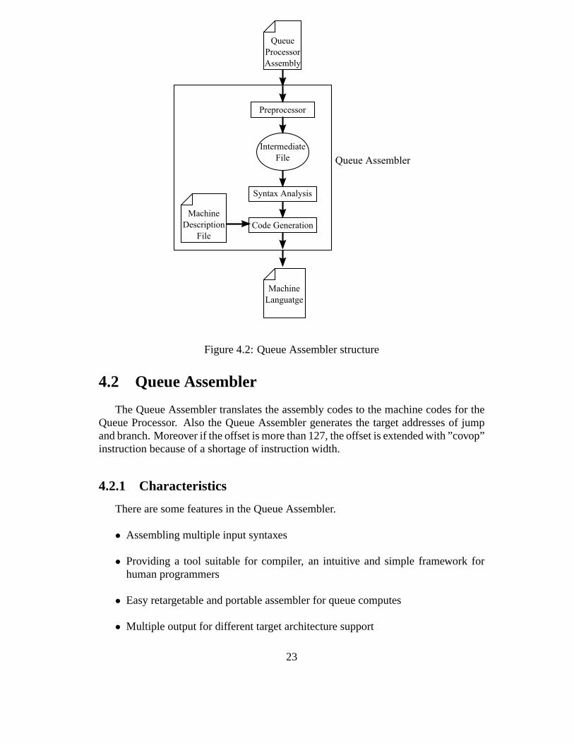
Figure 4.2: Queue Assembler structure
4.2 Queue Assembler
The Queue Assembler translates the assembly codes to the machine codes for theQueue Processor. Also the Queue Assembler generates the target addresses of jumpand branch. Moreover if the offset is more than 127, the offset is extended with ”covop”instruction because of a shortage of instruction width.
4.2.1 Characteristics
There are some features in the Queue Assembler.
• Assembling multiple input syntaxes
• Providing a tool suitable for compiler, an intuitive and simple framework forhuman programmers
• Easy retargetable and portable assembler for queue computes
• Multiple output for different target architecture support
23
4.2.2 Structure
The Queue Assembler is constructed by three phases: preprocessor, syntax analy-sis and generation. The first phase preprocessor translatesthe Queue Compiler outputto the intermediate file. The Queue Compiler output can not be allowed as the QueueAssembler input. The translated intermediate file is provided to the second phase, syn-tax analysis. The program is divided into tokens and these token are categorized withmachine description file. The categories are mnemonic, operand1, operand2, label andcomment. Finally the third phase generation translates thetokens into the machinecode with machine description file. The machine descriptionfile contains the somefields: mnemonic, opcode of the machine dependent, value andoffset. The machinedescription file is depends on the queue processor architecture. Thus the multiple out-put is supported by changing the machine descritption file. Also the ”covop” instruc-tion is supported in the Queue Assembler. To cover the instruction width shortage, the”covop” instruction extends the operand fields from 8-bit to16-bit. The operand fieldcan cover 16-bit width. Figure 4.2 shows the structure of theQueue Assembler.
4.3 Queue Simulator
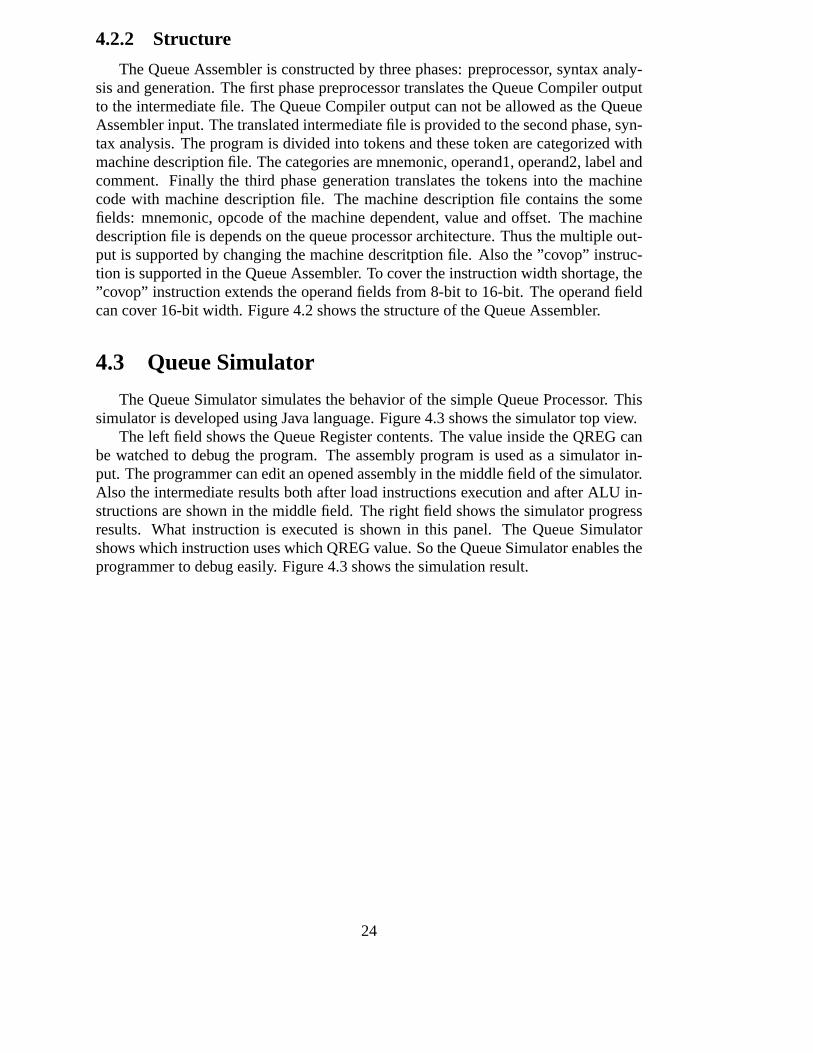
The Queue Simulator simulates the behavior of the simple Queue Processor. Thissimulator is developed using Java language. Figure 4.3 shows the simulator top view.
The left field shows the Queue Register contents. The value inside the QREG canbe watched to debug the program. The assembly program is usedas a simulator in-put. The programmer can edit an opened assembly in the middlefield of the simulator.Also the intermediate results both after load instructionsexecution and after ALU in-structions are shown in the middle field. The right field showsthe simulator progressresults. What instruction is executed is shown in this panel.The Queue Simulatorshows which instruction uses which QREG value. So the Queue Simulator enables theprogrammer to debug easily. Figure 4.3 shows the simulationresult.
24
Figure 4.3: Top view of the Queue Simulator
25

Figure 4.4: Simulation result: The intermediate QREG content is shown in middle,Simulator behavior is shown in right
26
Chapter 5
Design Result
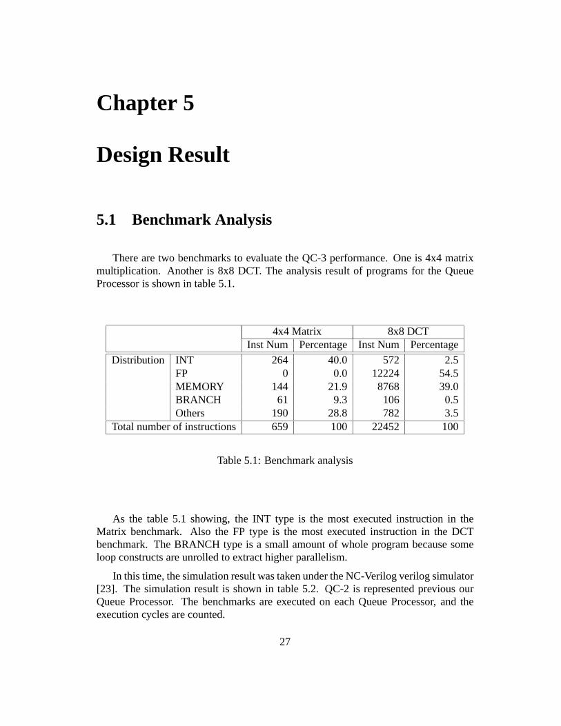
5.1 Benchmark Analysis
There are two benchmarks to evaluate the QC-3 performance. One is 4x4 matrixmultiplication. Another is 8x8 DCT. The analysis result of programs for the QueueProcessor is shown in table 5.1.
4x4 Matrix 8x8 DCTInst Num Percentage Inst Num Percentage
Distribution INT 264 40.0 572 2.5FP 0 0.0 12224 54.5MEMORY 144 21.9 8768 39.0BRANCH 61 9.3 106 0.5Others 190 28.8 782 3.5
Total number of instructions 659 100 22452 100
Table 5.1: Benchmark analysis
As the table 5.1 showing, the INT type is the most executed instruction in theMatrix benchmark. Also the FP type is the most executed instruction in the DCTbenchmark. The BRANCH type is a small amount of whole program because someloop constructs are unrolled to extract higher parallelism.
In this time, the simulation result was taken under the NC-Verilog verilog simulator[23]. The simulation result is shown in table 5.2. QC-2 is represented previous ourQueue Processor. The benchmarks are executed on each Queue Processor, and theexecution cycles are counted.
27
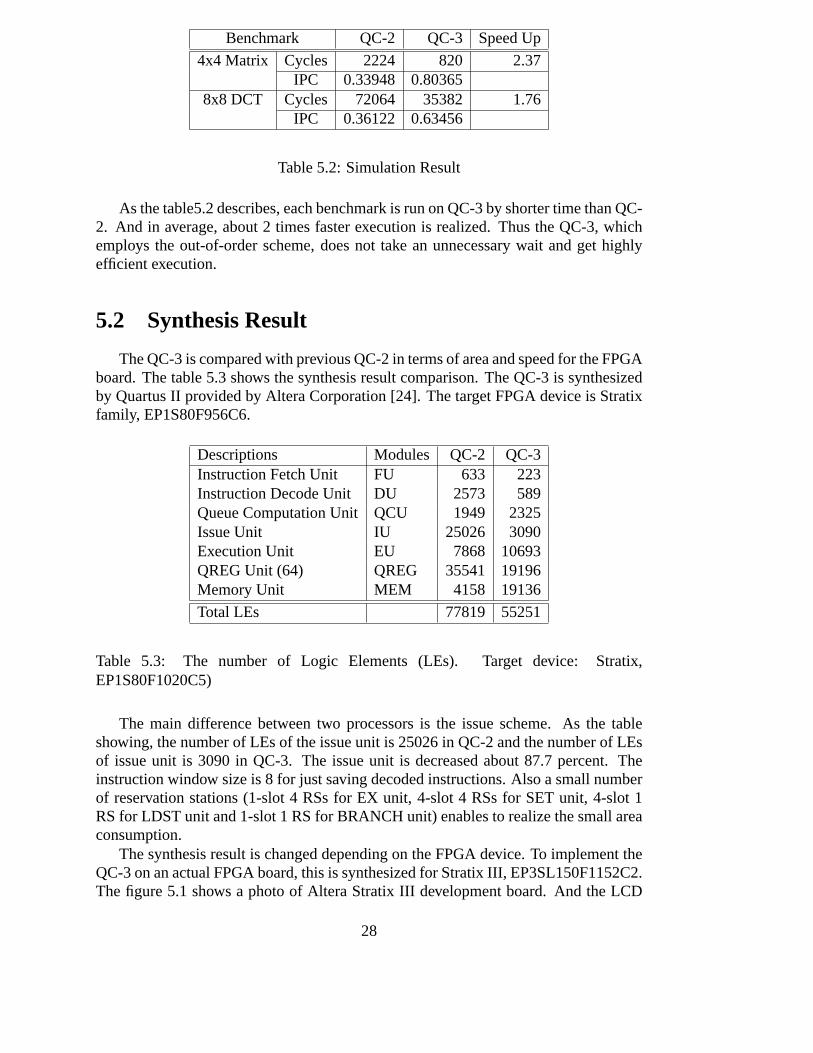
Benchmark QC-2 QC-3 Speed Up
4x4 Matrix Cycles 2224 820 2.37IPC 0.33948 0.80365
8x8 DCT Cycles 72064 35382 1.76IPC 0.36122 0.63456
Table 5.2: Simulation Result
As the table5.2 describes, each benchmark is run on QC-3 by shorter time than QC-2. And in average, about 2 times faster execution is realized. Thus the QC-3, whichemploys the out-of-order scheme, does not take an unnecessary wait and get highlyefficient execution.
5.2 Synthesis Result
The QC-3 is compared with previous QC-2 in terms of area and speed for the FPGAboard. The table 5.3 shows the synthesis result comparison.The QC-3 is synthesizedby Quartus II provided by Altera Corporation [24]. The targetFPGA device is Stratixfamily, EP1S80F956C6.
Descriptions Modules QC-2 QC-3Instruction Fetch Unit FU 633 223Instruction Decode Unit DU 2573 589Queue Computation Unit QCU 1949 2325Issue Unit IU 25026 3090Execution Unit EU 7868 10693QREG Unit (64) QREG 35541 19196Memory Unit MEM 4158 19136
Total LEs 77819 55251
Table 5.3: The number of Logic Elements (LEs). Target device: Stratix,EP1S80F1020C5)
The main difference between two processors is the issue scheme. As the tableshowing, the number of LEs of the issue unit is 25026 in QC-2 andthe number of LEsof issue unit is 3090 in QC-3. The issue unit is decreased about87.7 percent. Theinstruction window size is 8 for just saving decoded instructions. Also a small numberof reservation stations (1-slot 4 RSs for EX unit, 4-slot 4 RSs for SET unit, 4-slot 1RS for LDST unit and 1-slot 1 RS for BRANCH unit) enables to realize the small areaconsumption.
The synthesis result is changed depending on the FPGA device. To implement theQC-3 on an actual FPGA board, this is synthesized for Stratix III, EP3SL150F1152C2.The figure 5.1 shows a photo of Altera Stratix III developmentboard. And the LCD
28

display shows the QC-3 status, such as the program counter, the signals of memoryaccess, jump, branch, and halt. Also the clock is shown by blinking LED on the board.
Figure 5.1: Altera Stratix III development board
The synthesis result for Stratix III is shown in table 5.4. The ALUT represents forthe Advanced Look-Up Table, which is the cell of Stratix III FPGA device used as theoutput of logic synthesis. This ALUT is used for evaluating area.
Descriptions Modules ALUTs REGISERsInstruction Fetch Unit FU 124 220Instruction Decode Unit DU 283 272Queue Computation Unit QCU 1923 668Issue Unit IU 2489 978Execution Unit EU 6927 1765QREG Unit QREG 39813 9426Memory Unit MEM 269 0
Total 51828 13329
Table 5.4: Synthesis result of QC-3. Target device: Stratix III, EP3SL150F1152C2
The QC-3 achieves 63.12MHz as a maximum clock frequency. The total powerconsumption estimation result running the Matrix benchmark is 1267mW where thestatic power consumption is 569.7mW and the dynamic power is651.3mW when theclock frequency is 50MHz.
29
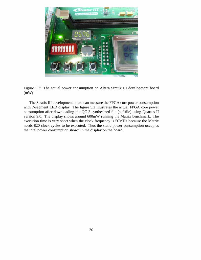
Figure 5.2: The actual power consumption on Altera Stratix III development board(mW)
The Stratix III development board can measure the FPGA core power consumptionwith 7-segment LED display. The figure 5.2 illustrates the actual FPGA core powerconsumption after downloading the QC-3 synthesized file (soffile) using Quartus IIversion 9.0. The display shows around 600mW running the Matrix benchmark. Theexecution time is very short when the clock frequency is 50MHz because the Matrixneeds 820 clock cycles to be executed. Thus the static power consumption occupiesthe total power consumption shown in the display on the board.
30
Chapter 6
Conclusion
In this thesis, the superscalar, out-of-order, produced order parallel queue proces-sor (QC-3) is designed. The issue unit generates the allocation information for eachreservation station, which holds the instructions. At thistime, to keep the order ofmemory and set register type instruction, the tag system is attached to instructions.The reservation station checks the true dependency using the queue register ready bit.If all operands are ready, the instruction in the reservation station is sent to the func-tional unit. The reservation station of the load store unit checks the set register unitcompletion signal and the tag. The reservation station compares the tags and if it ismatched, the matched instruction becomes ready. The queue processor does not waitunnecessary time to complete other independent instructions. Also the queue processorassigns the destination address of register in dynamic according to the queue compu-tation model. Thus the execution result is written into the queue register in any time.These systems enable the queue processor to get more high performance.
The performance evaluation using the 2 benchmarks, which are 4x4 matrix mul-tiplication and 8x8 DCT, shows 2 times faster execution time than previous queueprocessor. The area of the issue unit is also about 87 percentsmaller than previousone. The small issue unit enables the queue processor to get more high performance.Also the power is small. The total estimated power consumption is 1267mW, wherethe static power is 569.7mW and the dynamic power is 651.3mW,during executing thematrix benchmark. The FPGA board, which is Altera Stratix III development board,shows the FPGA core power consumption. After downloading the QC-3 running at50MHz as a clock frequency, its power display shows about 600mW. Also the briefanalysis of the Queue Compiler, the Queue Assembler, and Queue Simulator is shownin this paper.
31

Publication
1. Hiroki Hoshino, Abderazek Ben Abdallah, Kenichi Kuroda, ”Advanced Opti-mization and Design Issues of a 32-bit Embedded Processor Based on Pro-duced Order Queue Computation Model”, 2008 IEEE/IFIP International Con-ference on Embedded and Ubiquitous Computing, Shanghai, China, pp.16-22,Dec. 2008.
2. Hiroki Hoshino, ”Advanced Hardware Optimization Algorithms for High Per-formance Queue Processor Architecture”, Graduation Thesis, The University ofAizu, Feb. 2009.
3. Hiroki Hoshino, Taichi Maekawa, ”Simple Queue ProcessorSystem on ChipImplemented on the FPGA”, Technical Report, The University of Aizu, Oct.2009.
32
References
[1] B. Bisshop, T. Killiher, and M. Irwin, “The design of register renaming unit,” inVLSI1999, Proceedings of Great Lakes Symposium on VLSI, 1999.
[2] Shima D., “The design space of register renaming techniques,” in IEEE Micro,2002, pp. 70–83.
[3] Yeager C. Kenneth, “The Mips R10000 Superscalar Microprocessor,” inIEEEMicro, 1996, vol. 16, pp. 28–41.
[4] IBM PowerPC 740 / PowerPC 750 RISC Microprocessor User’s Manual.
[5] R.E. Kessler, “The Alpha 21264 microprocessor,” inIEEE Micro, 1999, vol. 19,pp. 24–36.
[6] M. Tremblay and J.M. O’Connor, “UltraSparc I: a four-issue processor support-ing multimedia,” inIEEE Micro, 1996, vol. 16, pp. 42–50.
[7] Bruno R. Preiss and V. C. Hamacher, “Data flow on a queue machine,” inISCA’85, 1985, pp. 342–351.
[8] Ben A. Abderazek, M. Arsenji, Soichi Shigeta, Tsutomu Yoshinaga, andMasahiro Sowa, “Queue processor architecture for novel queue computingpradigm based on produced order shceme,” inHigh Performance Computingand Grid in Asia Pacific Region HPCAsia’04, 2004, pp. p169–177.
[9] Hiroki Hoshino, Ben A. Abderazek, and Keniti Kuroda, “Advanced Optimizationand Design Issues of a 32-bit Embedded Processor Based on Produced OrderQueue Computation Model,” in2008 IEEE/IFIP International Conference onEmbedded and Ubiquitous Computing, 2008, pp. 16–22.
[10] Ben A. Abderazek, “The QC-2 Parallel Queue Processor Architecture,” Journalof Parallel and Distributed Computing, vol. 68, no. 2, pp. 235–245, 2008.
[11] B. A. Abderazek, S. Kawata, T. Yoshinaga, and M. Sowa, “Modular DesignStructure and High-level Prototyping for Novel Embedded Processor core,” inEUC 2005, The 2005 IFIP International Conference on EmbeddedAnd Ubiqui-tous Computing, 2005, pp. 340–349.
[12] B. A. Abderazek, T. Yoshinaga, and M. Sowa, “High-Level Modeling and FPGAPrototyping of Produced Order Parallel Queue Processor Core,” Journal of su-percomputing, vol. 38, no. 1, pp. 3–15, 2006.
33
[13] M. Fernandes, J. Llosa, and N. Topham, “Using queues forregister file organiza-tion in vliw,” Technical Report ECS-CSG-29-97, 1997, University of Edinburgh,Department of Computer Science.
[14] L. S. heath, S. V. Pemmaraju, and A. A. Trenk, “Stack and queue layouts ofdirected acyclic graphs: part i,” inSIAM journal of computing, 1996, pp. 1510–1539.
[15] A. Canedo, B. Abdallah Abderazek, and M. Sowa, “A new code generationalgorithm for 2-offset producer order queue computation model,” Journal ofComputer Languages, Systems and Structures, , no. Vol. 34, Issue 4, pp. 184–194, 2007.
[16] Jaume Abella and Ramon Canal, “Power- and complexity- aware issue queuedesign,” inIEEE Micro, 2003, pp. 50–58.
[17] R.M. tomasulo, “An efficient algorithm for exploiting multiple arithmetic units,”IBM Journal, pp. 25–33, January 1967.
[18] Subbarao Palacharla, Norman P. Jouppi, and J. E. Smith,“Complexity-effectivesuperscalar processors,” inISCA’97, 1997, pp. 206–218.
[19] Toshinori Sato and Itsujiro Arita, “Simplifying instruction issue logic in su-perscalar processors,” inthe Euromicro symposium on Digital System Design(DSD’02), 2002.
[20] Ben A. ABDERAZEK, Soichi SHIGETA, Kirilka NIKOLOVA, TsutomuYOSHINAGA, and Masahiro SOWA, “Fundamental Design of a Parallel QueueProcessor,” Tech. Rep., The Institute of Electronics, Information and Communi-cation Engineers, 2002.
[21] Masashi Masuda, “Graph transformation methods and theoretical performanceevaluation of queue computation models,” 2008.
[22] KUTLUK Halcham, Abderazek B. A., SHIGETA Soichi, YOSHINAGA Tsu-tomu, and SOWA Masahiro, “Analysis of Fundamental Characteristics of ParallelQueue Computation Model,” Tech. Rep., The Institute of Electronics, Informa-tion and Communication Engineers, 2004.
[23] Cadence Design Systems, “NC-Verilog verilog simulator,”http://www.cadence.com/.
[24] Altera, “Stratix FPGA series,” http://www.altera.com/.
34

Appendix A
Queue Core 3 Verilog-HDL code
The developed parallel queue processor (QC-3) is implemented in the VerilogHDLcode. The codes are atached in this appendix.
CODE DESCRIPTION
35