development of sic large tapered crystal growth · development of sic large tapered crystal growth...
TRANSCRIPT

Development of SiC Large Tapered Crystal Growth
Philip G. Neudeck NASA Glenn Research Center
May 15, 2012 Project ID # APE027
This presentation does not contain any proprietary, confidential, or otherwise restricted information
2
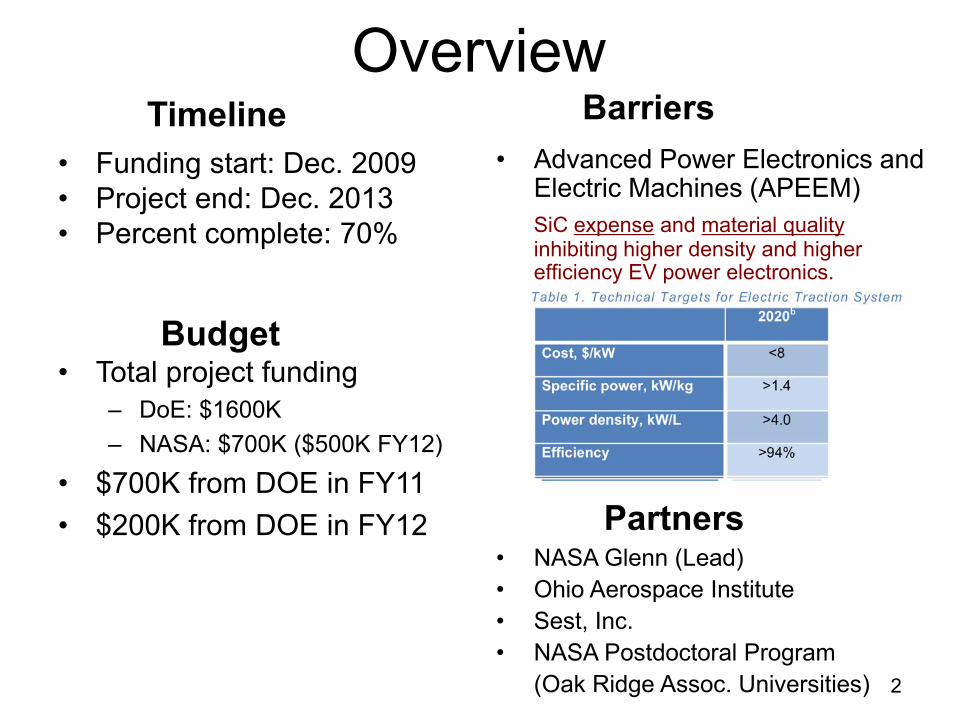
• Funding start: Dec. 2009 • Project end: Dec. 2013 • Percent complete: 70%
• Advanced Power Electronics and Electric Machines (APEEM)
SiC expense and material quality inhibiting higher density and higher efficiency EV power electronics.
• Total project funding – DoE: $1600K – NASA: $700K ($500K FY12)
• $700K from DOE in FY11 • $200K from DOE in FY12
Timeline
Budget
Barriers
• NASA Glenn (Lead) • Ohio Aerospace Institute • Sest, Inc. • NASA Postdoctoral Program (Oak Ridge Assoc. Universities)
Partners
Overview

3
•SiC power semiconductor devices should theoretically enable vastly improved power conversion electronics compared to today’s silicon-based electronics. •2-4X converter size reduction and/or 2X conversion loss reduction (theoretical performance gains vary with system design specifications). •Fundamentally improved implementation of smart grid, renewable energy, electric vehicles, aircraft and space power systems.
•SiC wafer defects and cost inherent to existing SiC material growth approach presently inhibiting larger benefits from becoming more widely available. •New but unproven NASA “Large Tapered Crystal” (LTC) SiC growth concept proposed to lower SiC material defect and cost technology barrier.
Objectives

4
Objectives
Funded Project Objective (Shorter Term) • Demonstrate initial feasibility of radically new “Large Tapered Crystal”
(LTC) approach for growing vastly improved large-diameter SiC semiconductor wafers.
• Verify needed (never experimentally demonstrated) LTC growth physics in laboratory setting:
• Growth of long, small-diameter single-crystal 4H-SiC fibers. • Lateral “M-plane” enlargement of 4H-SiC fibers into boules.
Overall Objectives (Longer Term) • Open a new technology path to large-diameter SiC and GaN wafers with 100-
1000 fold total crystal defect (dislocation) density improvement at 2-4 fold lower cost. (Present SiC wafers ~ 103-104 total dislocations per cm2.)
• Enable leapfrog improvement in wide bandgap power device capability and cost to in turn enable leapfrog improvements in electric power system performance (higher efficiency, smaller system size).

5
Milestones
Month/Year Milestone May 2011 Demonstrate epitaxial radial (lateral) growth of a 5 mm
diameter boule starting from a simulated SiC fiber crystal.
December 2011 Demonstrate laser-assisted fiber growth of a SiC fiber crystal greater than 10 cm in length.
First SiC experimental demonstrations of the two critical growth actions required for Large Tapered Crystal (LTC) process.
LTC is NOT viable without success of BOTH processes.
As discussed in this presentation, neither above quantitative milestone challenges have been met within the original project schedule.

DOE APEEM FY12 Kickoff Meeting
SiC seed
Present SiC Growth Process (Vapor transport)
Vertical (c-axis) growth proceeds from top surface of large-area seed via thousands of dislocations. (i.e., dislocation-mediated growth!)
Crystal grown at T > 2200 °C High thermal gradient & stress.
Limited crystal thickness.
Proposed LTC Growth Process
Vertical Growth Process: Elongate small-diameter fiber seed grown from single SiC dislocation.
Lateral Growth Process: CVD grow to enlarge fiber sidewalls into large boule. - 1600 °C, lower stress - Only 1 dislocation
Radically change the SiC growth process geometry to enable full SiC benefit to power systems.
Lateral & vertical growth are simultaneous & continuous (creates tapered shape).
(US Patent 7,449,065 OAI, Sest, NASA)
Approach/Strategy

Approach/Strategy (Solvent-LHFZ)- A New and Unique SiC fiber Growth Method
7
Feed Rod with Si + C + Solvent (Non-Crystalline Source Material)
Seed Crystal
Seed Holder
SiC Crystal Fiber
Combines the advantages of Traveling Solvent Method (TSM) & Laser Heated Floating Zone (LHFZ) • TSM: Known SiC growth method • LHFZ: Semi-infinite growth material
0.5 mm

8
Technical Accomplishments and Progress
• 88 Experimental Solvent-LHFZ runs since 2011 Review.
• 10 Changes to feed rod processing technique, 5 feed rod material compositions tested, 5 seed crystal configurations tested.
• Have achieved single crystal growth rates >100 µm/hour (polycrystalline > 400 µm/hour)
• Demonstrated control over growth rates.
Experimental Conditions* (M.P. = Feed Rod Melting Point)
Growth Rates (µm/hour)
Fe/Si C (at.%) M.P. (ºC) M.P.+90 ºC M.P.+190 ºC
M.P.+325 ºC
Fe/Si~0.35 8 1170 4 40 135+
16 1195 50 120 N/A
Fe/Si~1.9 8 N/A No growth
* Temperatures not corrected for emissivity. Woodworth et al., ICSCRM 2011

50 µm
Competing Growth Fronts
9
Technical Accomplishments and Progress
• Layer polytype confirmed via X-ray topography (Prof. Dudley @ SUNY)
• Non-ideal “cut seed” crystal growth front is large (~ 0.5 mm2).
• Many screw dislocations, many growth centers (not wanted for LTC).
• Chaotic growth front morphology is observed (likely creates defects).
300 µm 50 µm
Solvent-LHPG SiC Fiber Growth

10
20mm
6H-SiC pseudo fibers
4H/6H SiC a/m-plane slivers prior to growth
Post-growth crystals are translucent and exhibit lateral expansion (a/m-face growth).
3C-SiC crystallites (yellow) undesirably nucleated in some areas.
Slivers after 8 hours of CVD epitaxial growth
Technical Accomplishments and Progress Radial/Lateral CVD Epi-Growth
11
1mm g
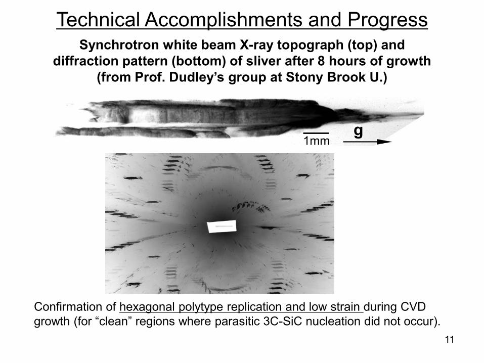
Synchrotron white beam X-ray topograph (top) and diffraction pattern (bottom) of sliver after 8 hours of growth
(from Prof. Dudley’s group at Stony Brook U.)
Technical Accomplishments and Progress
Confirmation of hexagonal polytype replication and low strain during CVD growth (for “clean” regions where parasitic 3C-SiC nucleation did not occur).

12
Technical Accomplishments and Progress
NASA Glenn SiC CVD Growth System Major Equipment Failure
(RF Generator) on August 12, 2011
Water cooled power diodes
Water Water
Soot
Soot
Water lines
- Heavily damaged sub-system returned to manufacturer for replacement/repair. - New RF generator procured (using $100K of NASA funds). - All lateral CVD SiC epitaxial growth work suspended for > 5 months. - Delayed new/improved seeding of Solvent-LHFZ growths. - Operations resumed using repaired sub-system on January 23, 2012. - 22 operational runs conducted in 36 working days following repairs.
Radial/Lateral CVD Epi-Growth

13
Technical Accomplishments and Progress
2011 Merit Review
Epi Growth Rate: ~80 µm/hour Max. Film Thickness: ~0.15 mm Max Diameter: ~1 mm (mostly seed) Rough grown surfaces/mini-facets
2012 Merit Review
2 mm
Epi Growth Rate: ~ 120 µm/hour Max. Film Thickness: ~2 mm Max Diameter: ~4 mm (mostly epi) (80% of 5 mm Quantitative Milestone) Smooth Tapered Hexagonal Facets!
Radial/Lateral CVD Epi-Growth
seed sliver 3C-SiC
Contamination from Susceptor
Smooth Tapered Hexagonal Facets

14
Proposed Future Work
Polycrystalline 3C-SiC
SiC coating failure
Carry out detailed characterization of larger mini-boules. - Including X-ray Topography by Prof. Dudley’s group at SUNY. - Answer critical question: Are stacking faults produced during thick radial CVD? CVD growth hardware & crystal mounting modifications to suppress 3C-SiC. Grow and characterize increasingly larger mini-boules.
Radial/Lateral CVD Epi-Growth

15
Proposed Future Work Fiber Growth
Transition to micro-patterned “single screw hexacone” (produced by patterned etching followed by CVD epi as described in LTC patent).
Smaller, well-ordered seed with pointed tip is needed for fiber growth.
P. Neudeck, 2009 DRIP Conf.
In addition to solvent-LHPG growth, LTC patent also describes laser-assisted vapor-growth methods for growing long single-crystal fiber (from same “hexacone” SiC seeds).
Free Form Fibers LLC (NY) – Initiating SBIR Phase III (NASA Funded $100K) for laser-assisted SiC fiber growth using gas precursors. • Small business presently laser-growing polycrystalline SiC fiber shapes. • Parallel path (risk mitigation) to realize single-crystal SiC fiber growth if
technical challenges of Solvent-LHFZ approach cannot be overcome.
Further refinement of seed rods (materials, smaller diameter) and solvent-LHPG growth process.

16
Collaboration and Coordination with Other Institutions • NASA Glenn Research Center (Prime) SiC crystal growth and ceramic fiber growth research branches
• Ohio Aerospace Institute (Non-Profit) • Sest, Inc. – SiC Crystal Characterization • NASA Postdoctoral Program (Oak Ridge Assoc. Universities)
• State University of New York at Stony Brook – National Synchrotron
Light Source at Brookhaven National Laboratory (Dept. of Energy) • Prof. Dudley’s group - recognized leader in X-Ray topographic
mapping characterization of SiC crystals and defect structure.
• Free Form Fibers LLC (NY) – Initiating SBIR Phase III (NASA Funded $100K) for laser-assisted SiC fiber growth using gas precursors.
• Small business laser-growing polycrystalline SiC fiber shapes. • Parallel path (risk mitigation) to realize single-crystal SiC fiber
growth if technical challenges of Solvent-LHFZ approach cannot be overcome.

17
• Experiments to investigate feasibility of revolutionary new “Large Tapered Crystal (LTC)” SiC growth approach are behind schedule, but significantly progressing towards demonstration goals.
Summary
Technical Area
2011 Status 2012 Status
Radial Growth System build-up complete First layers documented ~ 1 mm diameter ~80 µm/hour growth rate
First “Mini-boules” grown ~ 4 mm diameter ~125 µm/hour growth rate Desired hex facet evolution
Fiber Growth System build-up complete First Solvent-LHFZ layers
Solvent-LHFZ > 100 µm/hour Laser-CVD Effort Initiating
• Developmental acceleration expected with addition of NASA resources, expanded LTC development team.

18
Technical Acknowledgements
NASA LTC Co-Investigators: Andrew Woodworth (NPP), Ali Sayir (NASA), Fred Dynsys (NASA), Andrew Trunek (OAI), David Spry (NASA), and J. Anthony Powell (Sest)
NASA LTC Support Team: Tom Sabo, Michelle Mrdenovich, Beth Osborn, Kelly Moses, Chuck Blaha, Kimala Laster, Jim Mazor, Wentworth John, and Frank Lam

19
Technical Back-Up Slides (Note: please include this “separator” slide if you are including back-up technical slides (maximum of five).
These back-up technical slides will be available for your presentation and will be included in the DVD and Web
PDF files released to the public.)

0.1
1
10
100
1000
10 100 1000 10000
Silicon SiC Si Limit
SiC Limit
Device Blocking Voltage (V)
Spe
cific
On-
Res
ista
nce
(mΩ
-cm
2 )
~6X SiC Benefit has been achieved
~2X (100%) SiC benefit still to be realized
Commercial silicon devices operate near theoretical limit.
Unipolar Power Device Comparison
Above comparison does NOT take yield, cost, other relevant metrics into account.
SiC devices are ~2X voltage or current-density de-rated from theoretical material performance.
(Volume Production Commercial Devices)

SiC Wafer Material Defects 75 mm diameter SiC wafer with epilayer
Magnified view small area in middle of wafer imaged by Ultra-Violet Photoluminescence - Each white dot or line is a dislocation defect! - Average dislocation density ~104 per cm2
Over the past decade there have been numerous studies (including NASA GRC) linking degraded SiC power device performance, yield, and reliability to the presence of defects in the SiC wafer crystal.
Stahlbush et. al., Mat. Sci. Forum vol. 556 p. 295 (2007)
0.25 cm2 SiC Power Device Area

Crystal growth at moderate growth rate in lateral (radial) direction
Lateral growth
Tapered crystal/Boule moves upward continuously
Region No. 1
Region No. 2
Faceted tapered crystal
Region No. 3
No Growth Tapered Crystal/Boule holder
Completed Boule
Axial growth
6. Boule contains only one dislocation along its axis; the remainder of the boule is nominally defect-free.
Fast laser-assisted fiber growth in the axial (c-axis) direction on a columnar seed crystal
Small-diameter Columnar seed crystal
Features (one embodiment): 1. 3-Region growth apparatus for
3 different growth actions.
2. Region 1: Vertical (c-axis) growth on a very small diameter columnar portion (“Fiber Growth”).
3. Region 2: Lateral (m-direction) growth on fiber & tapered portion (“Lateral Growth”).
4. Region 3: No growth after LTC boule reaches desired diameter.
5. Growth rate of boule in c-axis direction equals fast growth rate of columnar seed crystal.
Simplified Schematic Cross-Sectional Representation
Production LTC SiC Growth System

23
Technical Accomplishments and Progress Previously reported build-up and safety reviews of laser-assisted fiber growth and radial epitaxial growth hardware are now complete.
Both systems are now operational and growing experimental SiC crystals!
Laser Assisted Fiber Growth Hot-Wall Radial Growth System
(Photos previously presented at FY11 VTP Kickoff Meeting)

24
Prior a-face/m-face SiC Growth Research Takahashi & Ohtani, Phys. Stat. Solidi B, vol. 202, p. 163 (1997).
Defects were found to increase as a-face growth proceeded. Attributed to low energy difference between stacking configurations on the growth surface. BUT – This prior work was physical vapor transport (PVT) growth at T > 2000 °C, high thermal gradient. Key LTC feasibility question – will stacking faults form in CVD, isothermal, T ~1600 °C?