development of wireless microcontroller ...docs.neu.edu.tr/library/6348511058.pdfdevelopment of...
TRANSCRIPT

DEVELOPMENT OF WIRELESS MICROCONTROLLER BASED FUNCTIONAL ELECTRONIC STIMULATION DEVICE FOR
DROP FOOT CORRECTION
A THESIS SUBMITTED TO THE GRADUATE SCHOOL OF APPLIED SCIENCES
OF NEAR EAST UNIVERSITY
by
DERVİŞ PAŞA
In Partial Fulfilment of the Requirements for the degree of Master of Science
in Biomedical Engineering
NICOSIA 2014

I hereby declare that all information in this document has been obtained and presented in
accordance with academic rules and ethical conduct. I also declare that, as required by these
rules and conduct, I have fully cited and referenced all material and results that are not
original to this work.
Name, Last name :
Signature :
Date:

i
ABSTRACT
Drop foot syndrome is general term for difficulty lifting the front part of the foot from the ground
which is a common problem that can lead to falls, trips and injuries in human life. It is usually
neuromuscular disorder that cause peroneal neuropathy between the neck and the fibula. In other
words drop foot problem is the loss of communication between the the peroneal nerve and
central nervous system which is enables the foot to make dorsiflexion . The patient cannot move
his/her foot upward the ankle or toes. Foot drop correction is generally achieved by electric
stimulation of the common peroneal nerve by sending a series of pulses at a given amplitude,
duration and frequency . For this purpose a wireless programmable microcontroller based, low-
power, low-cost, battery operated, high performance and portable electronic stimulation device
has been developed.
The stimulator has been designed to make correction on the foot drop syndrome, which is called
wireless FES device. In the traditional FES systems, sensors are placed inside the shoe sole
which are connected to a stimulator device using lead wires or cables. One of the biggest
disadvantages of the cabled systems is the cable complexity, and also device giving discomfort to
the patient during the walking, because of the cables around the shoe and the foot. The system
designed by the author is wireless and was developed by removing this cables from the device
and by using Radio Frequency (RF) transmitter/receiver pair to connect the sensors to the
stimulator device. For this reason, the patients can use this device more comfortably, and easier.
In the design of the wireless FES device, a force sensitive sensor, programmable microcontroller,
transmitter, receiver and electrodes are used. Stimulation amplitude, duty cycle, and frequency
of the output waveform can easily be adjusted by using switches. Also design has been
developed further by the addition of another second in-sole foot sensor underneath the metatarsal
heads so that device enabled reliable sensing in addition to walking on straight surfaces during
the stair climbing. The cost of the overall system is very low, because during the development
process standard microcontroller development systems, standard electronic equipments and
standard wireless components were used which are easily found in the market.
Keywords: Drop foot syndrome, foot drop, drop foot correction, wireless microcontroller based
stimulation, peroneal nerve stimulation, FES device.

ii
ÖZET
Düşük ayak sendromu , ayağın ön kısmının zorlukla yerden kaldırılmasının genel bir terimi olup
insan hayatında düşmelere, tökezlemelere ve yaralanmalara sebebiyet veren yaygın bir sorundur.
Genel olarak boyun ve fibula arasındaki peroneal nöropatiye neden olan bir nöromüsküler
hastalıktır. Başka bir deyişle düşük ayak sorunu peroneal siniri ile merkezi sinir sistemi
arasındaki iletişim kaybından dolayı,ayak bileğin bileğinin dorsifleksiyon yapamamasıdır. Bu
hastalar ayağını ayak bileğinden yukarıya doğru hareket ettiremez. Ayak düşmesi genellikle
peroneal sinirine belirli bir genlikte ve sıklıkta bir dizi elekktrik uyarımı göndererek
düzeltilebilir. Bu amaçla kablosuz programlanabilir, düşük-güçte, düşük maliyetli, bataryalı,
taşınabilir ve yüksek performanslı bir stimülatör dizaynı geliştirilmiştir.
Kablosuz FES cihazı olarak tanımlan stimülatör, düşük ayak sendromu düzeltmek için
tasarlanmıştır. Geleneksel sistemlerde, ayyakabı içerisine yerleştirilmiş olan bir kuvveteduyarlı
sensörün sayesinde hastanın adımları algılanmaktaydı ve bir kablo vasıtasıyla mikroişlemci
destekli cihaza verilmekteydi. Kablolu sistemlerin en büyük dezavantajları ise ayakkabıdan
cihaza bağlanan kablonun yürüme esnasında hastaya rahatsızlık vermesi ve kablo
karmaşıklığına sebep olmasıydı. Kablosuz FES sistemi geliştirilerek sensörler ve cihaz
arasındaki kablo ortadan kaldırılmış ve Radyo Frekansları(RF) ile alıcı/verici kullanılarak
kablosuz iletişim hattı sağlanmıştır. Böylece hastalar bu cihazı daha kolay ve daha rahatça
kullanabilmektedirler. Kablosuz FES cihazı tasarımda kuvvete duyarlı sensörler,
programlanabilir mikroişlemci, verici, alıci ve elektrotlar kulanılmıştır. Uyarım frekansı ,pals
genişliği ve dalga çıkış genliği cihaz üzerindeki düğmeler kullanarak kolayca ayarlanabilir.
Ayrıca dizayn dahada gelştirilerek ikinci bir kuvvet ölçüm sensörü ayağın metatars başlarının
altına eklenmiştir böylece cihaz düz yüzeylerde yürüme ek olarak merdiven tırmanma sırasında
güvenilir algılama sağlamıştır. Tasarımın genel sistem maliyeti düşüktür bunun sebebi tasarım
esnasında kolayca piyasada bulunan standart mikroişlemci sistemleri, standart elektrikli
ekipmanları ve standart kablosuz bileşenleri kullanılmasıdır.
Anahtar Kelimeler: Ayak düşmesi, düşük ayak, düşük ayak düzeltmesi, kablosuz
mikrokontrolör tabanlı uyarım, peroneal sinir uyarımı, FES cihazı

iii
ACKNOWLEDGEMENTS
First of all, I would like to express my sincere gratitude and special thanks to my supervisor Prof.
Dr. Doğan Ibrahim, the former head of biomedical engineering department who supported and
helped me to complete this thesis. Under his guidance, I successfully overcome many difficulties
and learn a lot about the electronic and medical devices.
Secondly, I would like to thank all Near East University educational staff and my teachers
especially to Assoc. Prof. Dr. Terin Adalı, the head of biomedical engineering department, who
gave me support and encouregment during my master education.
Thirdly, I would like to thank NEU Training and Research Hospital , Physical Medicine and
Rehabilitation Department staffs, especially to Assist. Prof. Dr. Pembe Hare Yiğitoğlu, who gave
me technical help and medical support during hospital trials.
Finally, I would like to thank my parents for their efforts and moral support especially my
mother and all my friends, also I would like to thank NEU which is my second big family, who
gave me an education and job opportunity in my life.

iv
TABLE OF CONTENTS
ABSTRACT...........................................................................................................................i
ÖZET.....................................................................................................................................ii
ACKNOWLEDGEMENT....................................................................................................iii
TABLE OF CONTENTS.....................................................................................................iv
TABLE OF FIGURES.........................................................................................................vii
CHAPTER 1 INTRODUCTION .......................................................... ..........................1
1.1.What is Functional Electrical Stimulation .................................................................. .1
1.2.What is Foot Drop ....................................................................................................... 2
1.3.Literature Review FES ................................................................................................ 2
1.4.Why Use FES Device?................................................................................................. 4
1.5.The Purpose of the Thesis ............................................................................................ 4
1.6.Briefly Operation Of The Wireless FES Device ........................................................... 5
1.7.Thesis Layout .............................................................................................................. 5
CHAPTER 2 ANALYZING THE DROP FOOT, GAIT CYCLE, AND THE
COMPONENTS OF THE FES DEVICE ...................................................................... 6
2.1.Diagnosis of Foot Drop ............................................................................................... 6
2.2.Pathophysiology of Foot Drop ..................................................................................... 6
2.3.Foot Biomechanics ...................................................................................................... 7
2.4. The Gait Cycle...................................................................................................... .........9
2.4.1.The Normal Gait Cycle .......................................................................................... 12
2.4.2.Gait Cycle Of Dropped Foot Patients .................................................................... 12
2.5.What Are The Benefits of FES Device? ..................................................................... 13
2.6.Main Components of a Typical FES Device .............................................................. 13
2.6.1.Sensors... ................................................................................................................ 14
2.6.1.1.Force Sensitive Sensors (FSR) ........................................................................... 14
2.6.1.2.Push Button Switches........................................................................................... 15
2.6.1.3.Tilt Sensors .......................................................................................................... 16
2.6.1.4.Goniometers ........................................................................................................ 16
2.6.1.5.(EMG) Electromyography sensors ....................................................................... 17
2.6.1.6.Accelerometers .................................................................................................... 17

v
2.6.1.7.Gyroscopes .................................................................................................... ......18
2.6.2.Stimulating Unit................. .............................................................................. .......19
2.6.2.1.Digital Controller.....................................................................................................19
2.6.2.2.High Voltage & Switching circuit ................................................................... .....20
2.6.2.3.Power Supply(Batteries) ...................................................................................... 21
2.6.3.Clinician Control Unit ............................................................................................. 21
2.6.4.User Control Unit: .................................................................................................. 22
2.6.5.Electrodes ............................................................................................................... 23
CHAPTER 3 THE DEVELOPED MICROCONTROLLER BASED WIRELESS FES
SYSTEM..............................................................................................................................25
3.1.Overview ................................................................................................................... 25
3.2.Hardware & Operation Of The Wireless FES device .................................................. 26
3.2.1.The Circuit Diagram Of The Wireless FES Device ............................................... 27
3.2.2.Ready for PIC Board ............................................................................................... 29
3.2.2.1.Microcontroller Processinng ................................................................................ 29
3.2.3.The PIC16F887 MCU ............................................................................................. 31
3.2.3.1.Memory Of PIC16F887.........................................................................................32
3.2.3.2.The Basic Features of PIC16F887 ........................................................................ 32
3.2.4.Wireless Communication Unit ................................................................................ 34
3.2.4.1.Xbee RF Module .................................................................................................. 35
3.2.4.2.Arduino Uno ........................................................................................................ 37
3.2.4.3.Arduino Fio ......................................................................................................... 40
3.2.4.4.The ATmega328 Microcontroller ......................................................................... 42
3.3.FES Algorithm and Software ..................................................................................... 44
3.4.Configuration Mode................................................................................................... 44
3.5.Running Mode ........................................................................................................... 44
3.6.Stimulation Algorithm ............................................................................................... 46
CHAPTER 4 :RESULTS AND DISCUSSION ............................................................. 48
4.1.Results ....................................................................................................................... 48
4.2.Future Work And Recommendations.......................................................................... 49
CHAPTER 5 CONCLUSION...........................................................................................50

vi
REFERENCES ..............................................................................................................51
APPENDIX A ................................................................................................................55
APPENDIX B ................................................................................................................74

vii
TABLE OF FIGURES
Figure 1.1. Wireless Microcontroller Based FES Device...............................................................1
Figure 2.1. Four Different Foot Movements. ................................................................................8
Figure 2.2. Upward & Outward, and Downward & Inward Foot Movements ..............................9
Figure 2.3. Typicall Eight Phases of the Gait Cycle.....................................................................10
Figure 2.4. A block Diagram of a Typical FES Device................................................................14
Figure 2.5. Force Sensitive Resistors ..........................................................................................15
Figure 2.6. 4-Directional Tilt Sensor...........................................................................................16
Figure 2.7. Flexible Goniometer....................................................................................................16
Figure 2.8. Model of the Lower Extremity With Muscles Included and Actual Subject with EMG
Electrodes Attached........................................................................................................................17
Figure 2.9. Triple Axis Accelerometer .........................................................................................18
Figure 2.10. 3-Axis Digital Gyroscope.........................................................................................18
Figure 2.11. 18 Pin PIC16F84 Microcontroller ............................................................................20
Figure 2.12. MC34063 8 Pins DC to DC Converter 3.0-40V Output Current 1.5A....... ............20
Figure 2.13 9V Rechargeable Battery ...........................................................................................21
Figure 2.14. 2X16 LCD Display Board........................................................................................21
Figure 2.15. Color Coding of the Electrode Cables ......................................................................23
Figure 2.16. Flexible Electrode Pads ............................................................................................24
Figure 3.1. The Wireless Microcontroller Based Fes Device.......................................................25
Figure 3.2. The Block Diagram of Wireless FES device...............................................................26
Figure 3.3. Circuit diagram of wireless FES device.....................................................................28
Figure 3.4. Ready for PIC Board .................................................................................................29
Figure 3.5. Selecting COM ports On Boatloader..........................................................................30

viii
Figure 3.6. Selecting the Hex. File ...............................................................................................31
Figure 3.7.Begin Uploading & Bootloading Progress Bar ...........................................................31
Figure 3.8. PIC16F887 Pin Configuration ...................................................................................32
Figure 3.9. The Communication Unit Arduino fio(left) & Arduino Uno(right)...................... ....35
Figure 3.10. 1mW XBee Wire Antenna................................. ....................................................35
Figure 3.11. Xbee X-CTU Program .............................................................................................36
Figure 3.12. Arduino Uno board...................................................................................................37
Figure 3.13.Arduino Fio................................................................................................................41
Figure 3.14. Atmega 328 Microcontroller....................................................................................44
Figure 3.15. Operational States of FES .......................................................................................45
Figure 3.16. The Fes software in Porgram Deccription Language...............................................46
Figure 3.17 FES Stimulation Envelope.......................................................................................47
Figure 4.1. A Photograph During The Hospital Studies ............................................................48

1
CHAPTER 1
INTRODUCTION
1.1. What is Functional Electronic Stimulation
Functional electronic stimulation (FES) is one of the most rapidly growing areas in
biomedical engineering. FES has been developed to help patients with neurological
disorders, including foot drop, to move more easily and comfortable. FES system works by
producing muscular contractions which is mimic natural voluntary gait movement by
supplying electric pulses to the nerveous system to stimulate paralayzed muscles either
externally (across the skin) or directly (if implanted) (Horsley,2012).
In other words, FES is a technique that causes a muscular contractions through the use of
an electric pulses. The human body naturally uses electrical currents to make body parts
move . When a part of the body needs to move, the brain sends electric pulses to the
nerves. The nerveous system, acting like electrical wires, relay these pulses to the muscles,
directing them to contract(muscle contraction). This muscle contraction causes the body
parts to move in a controlled, deliberate way. For example ; the elbow, ankle or finger
joints movements. FES allows muscles that have been partially paralyzed or paralyzed by
stroke to move body parts again or to make foot drop correction. In a case of any
disability like a stroke or any neurological diseases, some of these electrical signals do not
function as well as they should. In such cases FES is required to stimulate nervous system
to sends electrical signals to muscle contraction (Retrieved January 6, 2014, from
http://strokengine.ca/intervention/admin/patient/FES%20Upper%20ExtremityFamily%20
Information.pdf).
Figure 1.1. Wireless Microcontroller Based FES Device

2
1.2. What is Drop Foot
Drop Foot, sometimes called dropped foot or foot drop, is a general term for difficulty
lifting the front part of the foot . Drop foot is a common problem in people suffering from
stroke, (MS)multiple sclerosis, cerebralpalsy, or SCI where some of the motor functions
are lost. In other words foot drop is a neuromuscular disorder that effects the gait
performace , significantly. A healthy gait or a normal walking pattern depends on
biomechanical and nervous system features. Drop foot is identified by the disability to lift
the front part of foot(toe up) when it is brought forward during the gait swing cycle,
resulting in the foot being on the ground all the time. This condition is due to the loss of
communication between the the peroneal nerve and central nervous system which causes
lack of activity in the ankle dorsiflexion. Previous studies show that , regular use of a drop
foot stimulator strengthens the activation of motor cortical areas and residual descending
connections (Everaert et al., 2007).
1.3. Literature Review FES
Functional electronic device was initially referred to as Functional Electrotherapy by
Liberson in 1961. The first real effort was made by him to supply electronic stimulation as
an aid to recover function in a disabled persons. Liberson designed portable FES device to
treate foot drop by stimulating the peroneal nervce of hemiplegic patients suffering from
drop foot during gait,which is basically an electronic devices that can generate pulses with
the correct amplitude ,ferquency and duration in order to stimulate the damaged nerves
externally.In this condition ,a heel switch located under the feet of a patient's shoe, would
activate a FES system worn by the patient (Liberson et al.,1961).
In a typical application ,external electrodes , energized by an electronic device are
placed above the peroneal nerve. During wallking the heel switch triggered stimulation
then the pulses generated at the correct times cause the tibialis anterior muscle to be
contracted (dorsiflexion of the foot) during swing phase of the gait cycle and hence help
the patient prevent it from dragging on the ground and lift the foot (Broderick et
al.,2008).The new design was simple but ingenious stimulator started a new field of
rehabilitation of paretic patients which is defined FES system. Since then, multi-channel,
dual-channel and one- channel. Electrical stimulators have been designed, that generate
stimulation via implantable electrodes or transcutaneous, cutaneous. This designe used in
subjects with head trauma ,MS and stroke to enable opening of spastic hand and correct
unnatural walking pattern (Hart et al., 2006).
In SCI patients electric stimulaion is used for walking and standing. In tetraplegic patients
electric stimulaion enables functional grasping by the paralysed hands. Electronic
stimulation has been used also for pain relief systems. TENS, correction of healing of
pressure sores and juvenile-scoliosis , vascular wounds and ulcuses (Retrieved January 6,
2014, from http://ifess.org/proceedings/IFESS1998/IFESS1998_065_Stanic.pdf).

3
FES can be applied using external, percutaneous, or implanted electrodes.In external
application, a pair of self-adhesive electrodes are placed on and near the peroneal nerve in
the leg. The actual points of placement are important as it affects the strength and
efficiency of the stimulation and the patient comfort level. In the case of percutaneous
FES, an electrode is placed under the skin and close to the peroneal nerve with the aid of a
needle. Percutaneous FES is more effective than the external FES but its placement may
require medically qualified staff. Percutaneous FES is also prone to infection and it is
difficult to keep it in place for long times. Implanted FES is based on placing the
electrodes under the skin permanently by a small surgery. In some applications, the actual
stimulation device may also be implanted under the skin. Although this is suitable for long
term use, it has the disadvantages that as with the percutaneous FES, qualified medical
staff is required to implant the device and as with any type of surgery there is always the
risk of infection (Broderick et al., 2008). A comparison of percutaneous and external
stimulators during gait in a case report of a child with hemiplegic cerebral palsy . The rise
in dorsiflexion was greater with percutaneous stimulators (Pierce et al., 2004).
External FES remains the preferred mode of stimulation in the clinical settings A trial
contains hemiparetic, ambulatory and 32 chronic patients each with a single foot drop.
They received either physiotherapy or FES treatment sessions. In conclusion patients in the
electronic stimulation group walked significantly faster, more effective and efficiently
with the common peroneal stimulators than patients in the physiotherapy group.On the
other hand, there is no improvement in these parameters was measured in the FES group
when the stimulator was not used (Seifart et al., 2009). The effect of FES on gait in spastic
cerebral palsy. Clinically significant improvements occurred in three of the eight children
(Postans et al., 2005). The effects of external FES applied to the gastrocnemius-soleus
complex. The authors concluded that FES is effective in increasing impulse during
thepush-off phase of the gait cycle, but not in decreasing stiffness (Ho et al., 2005).
The orthotic versus therapeutic impacts of Functional Electronic Stimulation devices was
compared by the Van der Linden et al., In this study FES suplied to the ankle dorsiflexors
and quadriceps in fourteen children with cerebral palsy. For the orthotic impact of FES, a
statistically significant effect was found for the measurement of the deviation of overall
gaitcycle pattern from the normal. FES to the dorsiflexors ensued in a statistically
significant orthotic effect on peak dorsiflexion in swing phase and the foot-floor angle at
first contact. This study showed that FES implemented to the dorsiflexors ensued in
significant improvements in the gait cycle of patients with CP. On the other hand no long-
term treatment effect of using FES was found (Van der Linden et al., 2008).
In another research the therapeutic and orthotic impacts of a drop foot electronic
stimulator on gait performance of subjects with chronic non-progressive (stroke) and
progressive (MS) disorders was compared. As a result shown that, bothgroups had an
orthotic benefit from FES however the therapeutic impact ended for a shorter time in
progressive disorders (Stein et al., 2010).

4
In a systematic study of investigators the improvement of gait cycle in stroke patients with
foot drop during the (peroneus)peroneal nerve stimulation. As a result of the studies
investigators suggested that there is positive orthotic impact of FES on walking speed
(Kottink et al., 2004).
1.4. Why Use FES Device?
The researchers discuss functional interventions based on motor learning and brain
plasticity basis. Researchers specify the ultimate aim of the rehabilitation is to test and
design interventions after resultant in deterioration benefits sufficiently robust to be
reflected in functional activity and further in participation of life role.The Activity of the
central nervous system dependent the basis principles and plasticity, of the learning of are
shown below ;
Close to natural gait
Improve the life quality
Activation of muscles during walking
Focused caution in movement
Repetition of requested gait
Specificity in Practice and Training
The results of the investigations have shown that recovery is supported by motor
experience. Also repetition of movements has been determined as a key in relearning of
motor principles (Popovic and Sinkjae, 2007). Functional electronic stimulation may
simplify motor recovery with joint and muscle afferent feed-back with repetitive of the
human movements (Kroon et al., 2005). Peripheral stimulation can effect reorganization
in the brain. The afferent nerves and efferent nerves input from movement simplified by
FES can play an important role as a reminder on “how to perform movement properly”
(Hara, 2008).
Researchers aid Stimulator as obtaining the learning principles of motor for gait with
respect to the literature, stimulator has been developed to treat unnatural gait tone,
paralyzed muscles, in-coordination of motion, gait problems(foot drop patients). It can
closely increase the motor gait components . It does supply the “practice of close-to-
normal movement and repetition of that practice” ( Daly and Ruff, 2007).
1.5. The Purpose of the Thesis
The purpose of this thesis is to improve walking ability of patients who live with drop foot
condition due to spinal cord injury (SCI), Multiple Sclerosis (MS), head injury, stroke,
Cerebral palsy (CP) or other neurological disorders by using a wireless microcontroller
based FES device. Drop Foot is a condition characterized by weakness or paralysis of the
muscles involved in lifting the front part of the foot so foot drop can leads trips, falls,
slow inefficient walking and difficulty in walking. Therefore to solve all these indicated

5
negative impacts on the patients, a microcontroller based wireless FES device has been
developed. In other words a microcontroller based wireless FES device is designed to
stimulate electrical pulses on the paralyzed muscles to restore muscular contraction in
this way FES can be improved the patient's gait performance and also it solves the cable
complexity and foot sensors wire discomfort with the design of wireless system.
The wireless FES device has been designed according to the main requiremets that will
satisfy the followings:
Low-cost
Low power consumption
Battery operated
Easy to Portable
Wireless communication
Stand-alone with no external support, e.g. for configuration ...
1.6. Brief Operation Of The Wireless FES Device
Force sensitive resistors are placed inside the patient’s shoe (insole) where a transmitter is
also placed. The receiver is attached to a microcontroller based electrical stimulation
circuit . When the patient tries to walk and lifts his or her foot, the receiver side senses
the trasmitted signal and sends a triggering signal to the stimulation circuit (or the
controller). The controller then sends a stimulus signals to patient’s peroneal nerve at the
feet so that stimulation starts and the patient can walk. When patient’s foot strikes to the
ground stimulation is stopped automatically by microcontroller.
1.7. Thesis Layout
This thesis consist of 5 Chapters.
Chapter 1 is the introduction part and provides literature review about the topic.
Chapter 2 is analyzes the foot drop problem and contains general information about the
components, and benefits of the typical FES devices.
Chapter 3 gives information about the hardware and software of the microcontroller based
wireless FES system in details.
Chapter 4 presents the test results , future work and recommendations about the thesis.
Finally, Chapter 5 is the conclusion

6
CHAPTER 2
ANALYZING THE DROP FOOT, GAIT CYCLE, AND THE
COMPONENTS OF THE FES DEVICE
2.1. Diagnosis of Drop Foot
The first diagnosis of the drop foot frequently is define in routine physical examination
of people. Such diagnosis can be specified and confirmed by a persons that experts in the
health fields such as these medical professionals are ortopedist, physiatrist,
neurologist, podiatrist,neurosurgeon or thopedic spine surgeon. A person living with drop
foot will have difficulty walking on patients heel. Therefore a simple test of asking the
patient to dorsiflex may explain diagnosis of the foot problem. This is measured on a 0-5
scale that observes mobility. The lowest point zero will determine the highest point ad
whole paralysis five , will determine whole mobility. On the other hand there are other
trials that might aid to define diagnosis. These testing introduce an magnetic resonans
imaging ,computed tomography , EMG or MRN to assess the surrounding areas of
paralyzed nerves and the paralyzed nerves them-selves, respectively. The nerve that
communicates to the muscle sytems that move the foot is the peroneal nerve. This nerve
trigger the anterior muscles of the leg that are used in dorsiflexions. The muscle that are
used in plantar flexion are triggered by the nerve in tibia and often develop tightness in
the presence of drop foot. Paraesthesia in the lower leg, particularly on the top of the ankle
and foot, also can cause foot drop, while it isn’t related every time (Retrieved January 6,
2014, from http://en.wikipedia.org/wiki/Foot_drop).
2.2. Pathophysiology of Drop Foot
Neurologic disorders are all reason of the foot drop disease , it should be approached using
a localization focused approach before etiologies are conceived by the medical
professionals. Mostly, drop foot is the result of neurological lesions which are effecting
the muscular contraction, only rarely is the non-functionality of the muscles or diseased
muscles. In other words Dropped foot is the inability to dorsiflex . The source for the
neurologic impairment can be central or peripheral. Dropped foot is rarely the result of a
pathologsiology including the muscles or bones which make up the lower leg. The
anterior tibial is the muscle that picks up the foot. It is triggered by the deep
fibular peroneous which branches from the sciatic nerves. The sciatic nerve exits the
lumbar plexus with its root arising from the 50 lumbar nerve space. Occasionally,
spasticity in the muscles opposite the anterior tibialis exists in the presence of dropped
foot, making the pathology much more complicated than dropped foot . Isolated foot drop
is mostly a flaccid conditions. Foot drop is diverse from foot slap, which is the audible
slapping of the foot to the ground with every step that exits although the foot initial contact

7
to the ground on each step, while they frequently are synchron. Also treated
systematically, possible lesion sites causing foot drop as explained below:
1. Peroneal nerve; (-chemical, mechanical, disease)
2. Genetical disease;
3. Neuromuscular disease;- affecting the muscles or affecting their direct nervous
system control
4. Sciatic nerve;(-direct trauma, iatrogenic)
5. Lumbosacral plexus;- lumbar plexus,sacral plexus,pudendal plexus causes sensory
deficits, and loss of motor control .
6. Nerve roots(L5)
7. Spinal cord; (Tumor,poliomyelitis)
8. Stroke, TIA, tumor;
9. Nonorganic;
10. Syndrome of the Cauda Equina. (Spinal cord injury reason of the nerve
impingement);
11. An others( multiple sclerosis, trauma, motor neuron disease, diabetes, and side
effects of the alcohol or drug.(Retrieved January 6, 2014, from http://en.wikipedia.
org/wiki/Foot_drop).
2.3. Foot Biomechanics
The "biomechanics" word was coined in 1899 by Nikolai Bernstein. Biomechanism is the
study of the function and structure of biological systems such as plants,animals,humans,
organs, and cells by means of the science methods of mechanics.Biomechanics is related to
engineering and motion of bodies, because it frequently uses conventional engineering
sciences to investigate the biological systems. Some examples of Newtonian mechanics or
materials sciences can supply correct approximations to the mechanics of many biological
systems. Most notably mechanical engineering is applied mechanics, it is discipline such
as structural analysis, continuum mechanics, mechanism analysis, kinematics and
dynamics which are play important role in biomechanic studies (Retrieved January 6,
2014, from http://en.wikipedia.org/wiki/Biomechanics).
In other words mechanincs is the branch of physics related with the motion of bodies, in
case of biomechanics, the bodies are living as bio = life. So, foot biomechanics basically,
relates to the study of foot movements and the effects of muscles and gravity on its skeletal
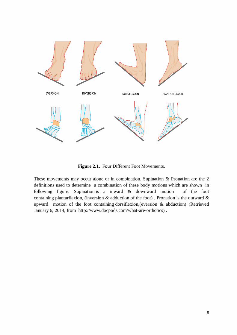
structure. A foot can dorsiflex (move upwards) and plantarflexion (downwards);
Adduction (horizontally inwards) and Abduction(horizontally outwards); Eversion (twist
outwards) and Inversion (twist inwards) (Retrieved January 6, 2014, from
http://www.docpods.com/what-are-orthotics).
8
Figure 2.1. Four Different Foot Movements.
These movements may occur alone or in combination. Supination & Pronation are the 2
definitions used to determine a combination of these body motions which are shown in
following figure. Supination is a inward & downward motion of the foot
containing plantarflexion, (inversion & adduction of the foot) . Pronation is the outward &
upward motion of the foot containing dorsiflexion,(eversion & abduction) (Retrieved
January 6, 2014, from http://www.docpods.com/what-are-orthotics) .
9
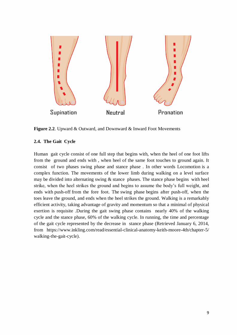
Figure 2.2. Upward & Outward, and Downward & Inward Foot Movements
2.4. The Gait Cycle
Human gait cycle consist of one full step that begins with, when the heel of one foot lifts
from the ground and ends with , when heel of the same foot touches to ground again. It
consist of two phases swing phase and stance phase . In other words Locomotion is a
complex function. The movements of the lower limb during walking on a level surface
may be divided into alternating swing & stance phases. The stance phase begins with heel
strike, when the heel strikes the ground and begins to assume the body’s full weight, and
ends with push-off from the fore foot. The swing phase begins after push-off, when the
toes leave the ground, and ends when the heel strikes the ground. Walking is a remarkably
efficient activity, taking advantage of gravity and momentum so that a minimal of physical
exertion is requisite .During the gait swing phase contains nearly 40% of the walking
cycle and the stance phase, 60% of the walking cycle. In running, the time and percentage
of the gait cycle represented by the decrease in stance phase (Retrieved January 6, 2014,
from https://www.inkling.com/read/essential-clinical-anatomy-keith-moore-4th/chapter-5/
walking-the-gait-cycle).

10
Figure 2.3. Typicall Eight Phases of the Gait Cycle
(Retrieved January 6, 2014, from https://www.inkling.com/read/essential-clinical-
anatomy-keith-moore-4th/chapter-5/walking-the-gait-cycle).

11
Table 2.1. Muscular Activities During Gait Cycle (Rose et al., 1994).
Mechanical Goals Active Muscle Groups
S Lower forefoot to ground Ankle dorsiflexors (eccentric contraction)
T Continue deceleration (reverse forward swing) Hip extensors
A Intrinsic muscles of foot
N Long tendons of foot
C Accept weight Knee extensors
E Decelerate mass Ankle plantarflexors
Stabilize pelvis Hip abductors
P Intrinsic muscles of foot
H Long tendons of foot
A Stabilize knee Knee extensors
S Control dorsiflexion (preserve momentum) Ankle plantarflexors (eccentric contraction)
E Stabilize pelvis Hip abductors
Preserve longitudinal arch of foot Intrinsic muscles of foot
Accelerate mass Ankle plantarflexors (concentric contraction)
Stabilize pelvis Hip abductors
Intrinsic muscles of foot
Long tendons of foot
Accelerate mass Long flexors of digits
Intrinsic muscles of foot
Long tendons of foot
Decelerate thigh; prepare for swing Flexor of hip (eccentric contraction)
S
W
I
N
G Clear foot Ankle dorsiflexors
P Midswing Clear foot Ankle dorsiflexors
H Decelerate thigh Hip extensors (eccentric contraction)
A Decelerate leg Knee flexors (eccentric contraction)
S Position foot Ankle dorsiflexors
EExtend knee to place foot (control stride);
prepare for contactKnee extensors
Flexor of hip (concentric contraction)
Terminal swing
Terminal stance
(heel off)
Preserve arches of foot; fix forefoot
Preswing (toe
off)Preserve arches of foot; fix forefoot
Initial swing
Accelerate thigh, vary cadence
Phase of Gait
Heel strike
(initial contact)
Preserve longitudinal arch of foot
Loading
response (flat
foot)
Preserve longitudinal arch of foot
Midstance

12
2.4.1. The Normal Gait Cycle
The natural gait cycle is as shown below in sequencely;
Swing Phase: During the movement it defined as the period of time when the foot is not in
contact with the ground. In those cases while the foot never leaves the ground (foot strike),
it can be defined as the phase when all portions of the foot are in forward motion.
Initial Contact : The point in the gait cycle where the foot initially makes contact with
the ground; this specifies the beginning of the stance phase. It is suggested that heel strike
not be a term used in clinical gait analysis as in many circumstances initial contact is not
made with the heel. Suggestion: Should use foot strike.
Terminal Contact : The point in the gait cycle while the foot leaves (foot-rise) the
ground: this specifies the beginning of the swing phase or end of the stance phase .
Additionally referred to as foot rises or foot off . Toe off should not be used in situations
where the toe is not the last part of the foot to leave the ground (Retrieved January 6, 2014,
from http://en.wikipedia.org/wiki/Biomechanics).
2.4.2. Gait Cycle Of Dropped Foot Patients
Drop foot gait cycle requires more exaggerated phases as explained below in sequencely;
Dropped Foot Swing Phase: During the walking cycle if the foot happens to be the
affected foot, there will be greater flexion at the knee to accommodate the disabilty to
dorsiflex. This increase in knee extension will cause a stair climbing movement.
Dropped Foot Initial Contact: First contact of the foot that is in movement will not have
natural heel toe foot strike. Instead of the foot may either slap the ground or the overall
foot may be located on the ground all at once.
Dropped foot Terminal Contact: Terminal contact that is observed in patients that have
dropped foot is quite different. Since patients tend to have weakness in the affected foot,
they may have the disability to support weight of body. Frequently, a cane or walker will
be used to assist in this aspect.
The part of the dropped foot gait cycle that introduces most dorsiflexion of the muscle
would be Heel Contact of the foot at ten percent of Gait Cycle, and the overall swing
phase, or between sixty-hundrend percent of the Gait Cycle. This is determined as a Gait
Abnormalitie(Retrieved January 6, 2014, from http://en.wikipedia.org/wiki/Biomechanics).

13
2.5. What Are The Benefits of FES Device?
Trials have shown that stimulation for foot drop can lead to the following benefits:
Provides more natural walking pattern
Regenerated walking speed
Increased independence during daily activities
Walking becomes less tiring
Improved self confidence and safety with a reduced incidence of falls
Increased independence during daily activities and ability to walk longer distances
Reduced spasticity and Curative effect
Walking becomes easier on uneven surfaces
This impact might not relate with every users or be stable. Many Foot drop patients
resulted that these benefit supply them to enjoy a better qualification in life & gait cycle .
The evidence from these studies was reviewed by the National Institute for Health and
Clinical Excellence . Their published guidance states that dropped foot electric stimulation
is a effective and safe treatments. The “National Clinical Guideline for Stroke” reported by
the Royal College of Physicians also recommends dropped foot electric stimulation
(Retrieved January 6, 2014, from http://www.differentstrokes.co.uk/content/ helpingyou/
professionals/Adult%20info/FES.pdf ).
2.6. Main Components OF a Typical FES Device
Functional Electronic Stimulation systems must meet specific design requirements to
supply orthotic or therapeutic impacts and to help patients. To function as a take-home
device, FES must be easily operable,be safe, portable, comfortable and so that users can
wear the device without any help or with minimal assistance or aid. The interface must be
as ergonomic as possible to enable patients with minimize poor eyesight or dexterity to
use the device without any difficulty. Most surface FES systems follow a standard
electronic design structure, similar to that originally proposed by author , system consisting
of sensors , stimulating parts, user interface ,clinician interface and electrodes In general,
modern FES devices consist of five main parts these are shown below ( Ilic et al., 1994).
Sensors: To detect gait events
Stimulating Unit: Provides electrical pulses to a certain nerve points.(digital
controller, a high voltage or current generation and switching circuitry, and
battery).
Clinician Control Unit: Clinician enables the stimulation features to be set for the
user.
User Control Unit: To change the output amplitude, frequency and duration
settings for specific user requirements.
Electrodes : Placed on peroneal nerve which is used to apply stimulus to the
patient.

14
Figure 2.4. shows the block diagram of a typical modern FES device which are included
the basic elements of the FES designing.
Figure 2.4. A block Diagram of a Typical FES Device
2.6.1. Sensors
Sensors are the basic requirements of the FES devices to determine the patient’s
activities. All FES systems consit of various sensors to detect activities when the stimulus
should be applied to the paralyzed muscles .Some commonly used sensor types are shown
below:
Force Sensitive Sensors or Force Sensisitve Resistor (FSR)
Push Button Switches
Tilt Sensors
Goniometers
(EMG) Electromyography Sensors
Accelerometers
Gyroscopes
2.6.1.1.Force Sensitive Sensors (FSR)
Force sensitive sensor are also known as force sensitive resistor these sensors consist of
a conductive polymers, which changes resistance in a presumable manner following
application of force on its surface. FSR sensors are in-shoe sensors and are fitted to an in-
sole to detect movements of the foot . The controller assembly is usually kept in the
pocket or is attached to a belt around the body and these sensors are normally connected to
the microcontroller with a pair of wires or connection can be established via wireless
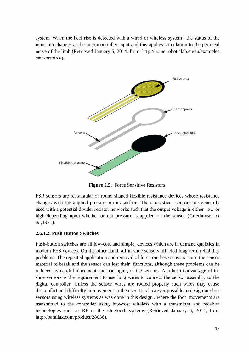
15
system. When the heel rise is detected with a wired or wireless system , the status of the
input pin changes at the microcontroller input and this applies stimulation to the peroneal
nerve of the limb (Retrieved January 6, 2014, from http://home.roboticlab.eu/en/examples
/sensor/force).
Figure 2.5. Force Sensitive Resistors
FSR sensors are rectangular or round shaped flexible resistance devices whose resistance
changes with the applied pressure on its surface. These resistive sensors are generally
used with a potential divider resistor networks such that the output voltage is either low or
high depending upon whether or not pressure is applied on the sensor (Griethuysen et
al.,1971).
2.6.1.2. Push Button Switches
Push-button switches are all low-cost and simple devices which are in demand qualities in
modern FES devices. On the other hand, all in-shoe sensors affected long term reliability
problems. The repeated application and removal of force on these sensors cause the sensor
material to break and the sensor can lost their functions, although these problems can be
reduced by careful placement and packaging of the sensors. Another disadvantage of in-
shoe sensors is the requirement to use long wires to connect the sensor assembly to the
digital controller. Unless the sensor wires are routed properly such wires may cause
discomfort and difficulty in movement to the user. It is however possible to design in-shoe
sensors using wireless systems as was done in this design , where the foot movements are
transmitted to the controller using low-cost wireless with a transmitter and receiver
technologies such as RF or the Bluetooth systems (Retrieved January 6, 2014, from
http://parallax.com/product/28036).

16
2.6.1.3. Tilt Sensors
Tilt sensors is a simplified accelerometer that can be found in various shapes and sizes and
they are small two state devices which change state when tilted. These sensors are
generally based on the movement of liquid (e.g.mercury) to make short circuit a pair of
contacts when tilted. When tilt sensors are compared with the in-shoe sensors they have
advantages over in-shoe as they do not suffer from reliability problems when used
repeatedly, and they can be miniaturized, which is a desirable property in FES applications.
But, like the in-shoe sensors these devices are not intelligent as they provide only high/low
(logic 1-0) type of output (Prieto et al., 1993).
Figure 2.6. 4-Directional Tilt Sensor
2.6.1.4.Goniometers
Goniometers sensors are used to measure 1D or 2D angular displacements (angles). it can
be used on most body joints e.g. knee, hip, ankle, shoulder, spine and elbow angles.These
sensors are used successfully in FES devices to measure the knee angle and trigger the
stimulation of FES device (Kostov et al., 1995). Some investigators used goniometers to
measure kinematic variables as an inputs at the ankle, knee, and hip joints with a fuzzy
model so that to determine the gait cycle (Chizeck, 1997).
Figure 2.7. Flexible Goniometer

17
2.6.1.5. (EMG) Electromyography sensors
Electromyography (EMG) sensors are used to measure electric potential of muscle
activities by using electrodes in FES devices. EMG sensors output very low analog
voltages that specify muscle activity. The main problem with EMG sensors is that it may
be difficult to generate a measurable EMG electric potentials on the damaged limb. As a
result of Naomi and William’s research it is also difficult to process the EMG signals as
special digital signal processing algorithms are required to remove stimulus artifacts and
generate useful electric signals in spinal cord injured (Chesler et al., 1997).
Figure 2.8. Model of the Lower Extremity With Muscles Included and Actual Subject with
EMG Electrodes Attached.
2.6.1.6.Accelerometers
Accelerometers are inexpensive electronic devices. These devices are used to measure the
magnitude and direction of acceleration in one to three linear axes (x, y, z) . These are tiny
microchips that mostly generate analog or digital voltages for each x,y,z direction . They
are proportional to the magnitude of the acceleration experienced by the FES device.
Several researchers they have been recommended to use, accelerometers as FES sensor
devices instead of in-shoe sensors. Accelerometers are mostly placed on the waist, on the
knee, or on the lumbar region. Accelerometers are intelligent sensors as they can be used to

18
sense the acceleration as well as the movement and the velocity of the leg in any direction
in x,y,z, axes (Williamson and Brian, 2000).
.
Figure 2.9. Triple Axis Accelerometer
2.6.1.7.Gyroscopes
Gyroscopes are tiny (MEMS) Micro-Electro-Mechanical Systems devices which are used
to measure angular velocity , this device do not have a fixed reference, and only measure
changes. MEMS are determined as devices that converts energy from one form to another
form. In these case of microsensors, the device basically converts a measured mechanical
signals into an electric signals. Pappas et al. have reported the successful use of gyroscopes
as sensors in FES devices. Gyroscopes are usually used with other sensors, such as with
force sensitive resistors and with accelerometers. As a result of research the quantitative
motion analysis during walking of the affected and nonaffected sides indicated that the use
of the combined in-sole and electric stimulation device showed that significant
improvement in the kinematics of gait at the affected limbsides. This stimulation system
and combined sensor has the potential to serve as a walking aid for rehabilitation training
or continued use in a wide range of gait disability after SCI, brain injury, stroke, or any
neurologic disorders (Pappas et al., 2004).
Figure 2.10. 3-Axis Digital Gyroscope.

19
2.6.2. Stimulating Unit
Stimulating units provides electrical pulses to a certain nerve points during the gait. Simply
stimulation unit is reasponsible from generation of stimulus signal. The controller sends a
stimulus signal to patient’s peroneal nerve so that stimulation starts and patient can walk.
When patient’s heel strikes to the ground stimulation is stopped by microcontroller. The
stimulation unit consist of digital controller, a high voltage or current generation and
switching circuitry, and battery which are described below ( Ilic et al., 1994).
2.6.2.1. Digital Controller
The main objective of the digital controller is to generate pulses at the output with the
specified frequency and pulse duration. Also, digital controllers must do the timing
control, user interface control, and gait detection. All digital controller based FES devices
consists of a microcontroller, which is fundamentally a single chip computer. There are
some components that affect the choice of a suitable microcontroller, such as the data
memory, size of the program ,power consumption, built-in clock, interrupt logic, and timer.
Since electrical stimulation devices are easly portable and are used in daily activities, long
battery life is one of the most important factor that impact the choice of the microcontroller
and interface circuitry. The total power consumption can be reduced by the choice of low
power elements wheresoever possible. For example, if LCD used it can be turned OFF
during normal operation to save device energy . The timing of the output pulses are
transmitted out using the built-in microcontroller timers. Generally more than one timer is
needed to create pulses with the required duration and frequency. Interrupt capability is
also an important parameter in the choice of the microcontroller since accurate timing is
mostly handled by using the timer interrupt mechanisms. The chosen microcontroller must
also have additional input-output ports, for example to drive an external display such as an
LCD, and also to accept inputs from sensors and various switches that may be used to
configure the device for specific user needs.There are lots of microcontroller families that
can be used in FES manufacturing as long as they provide the fundamental needs which
are summarized above. Some examples are the PIC series of microcontrollers, 8051 &
68HC11 series of microcontrollers, Atmega 328 series of microcontrollers, BX-24, and so
on. Some microcontroller examples that have already been generated in electronic systems
are: Microchip Technology's PIC16F84, Freescale 68HC11,Analog Devices ADuC831,
and BX-24 ( Breen et al., 2009).

20
Figure2.11. 18 Pin PIC16F84 Microcontroller
2.6.2.2. High Voltage & Switching circuit
In response to signals which is detected from the sensors, the microcontroller provides the
required stimulus current (output waveforms) at the correct times as low level output
voltages for stimulation. The High Voltage & Switching circuit is then controlled to
increase this stimulus current or voltage to the required level. Switching circuit generally
consists of a DC to DC converter and transformers to convert low voltage level to the high
voltage level, for example; + 9 V to + 80 V. The output of FES devices can be either
constant voltage or constant current. In a constant voltage device, the pulse amplitude is
around 80 V and the skin resistance increases if the current is lowered. Constant current
devices supply around 120 mA current and they are less affected from changing of skin
resistance . The output waveform from the FES devices is a pulse with a changeable pulse-
duration and frequency. The pulse shape can be monophasic, take sahpe from positive
pulses only, symmetric or asymmetric biphasic, where the pulses are both positive and
negative with no gap in between them, and symmetric biphasic with inter pulse intervals.
The pulse duration between 50 µs − 1 ms, and the pulse frequency in most devices change
between 1 − 100 Hz (Dimitrijevic et al., 2002).
Figure 2.12. MC34063 8 Pins DC to DC Converter 3.0-40V Output Current 1.5A

21
2.6.2.3.Power Supply (Batteries)
The electrical current of the FES device is created by a small battery powered electronic
circuits. The stimulator are portable and they are powered using either normal or
rechargeable batteries. Patient safety is an important parameter when the batteries are
charged while the device is worn by the patient movement. Because the FES devices are
used repeatedly during the gait they should be designed to increase battery life so that they
can be used for long periods . While design of the FES device, careful choice of a low-
power components and low-power microcontroller will result in long battery life. Some
FES systems for example “Parastep” make external belt worn rechargeable battery to
power the system for long period, while some other systems use single use or disposable
batteries for example” WalkAide” for protection. While using an external battery might
provide longer period during use of device, and also batteries are heavy and it is not
practical to carry them long time (Retrieved January 6, 2014, http://www.walkaide.com/en
-US/support/Documents/ ClinicianManual.pdf).
Figure 2.13 9V Rechargeable Battery
2.6.3. Clinician Control Unit
The clinician control unit enables the stimulator parameters to be set for the patients. It is
also interfaces with the clinician’s programmer, clinicians do adjustments that are
automatically stored in the patient’s records, to observe gait history and monitor patient
accordance with the FES device. In addition, displays (LCD) are usually provided to
make the device user-friendly, to see such changes in frequency, output amplitude and
duration settings on the device (Retrieved January 6, 2014, from http://uk.farnell.com/
mikroelektronika /mikroe-55/display-board-lcd-2x16/dp/2281679 ).
Figure 2.14. 2X16 LCD Display Board.

22
2.6.4. User Control Unit
The user control unit enable users to control the on-off switch, intensity and also to
adjust the output amplitude, frequency and duration settings for specific requirements of
the patients. In addition the resistance of the muscular contraction is controlled by the
pulse amplitude,duration and frequency of the stimulus generated by FES devices.
User Parameters for Frequency Pulses
Patients reguire a high enough, fusion frequency, to create a smooth contraction. It
must produce too low and series of twitches.
Temporal summation is the cumulative effect of stimuli repeated in a short time
interval
If the applied stimulus frequency is high , it effects the muscles contraction more
stronger and at the same time it result with quickly increase in muscle fatigue.
The minimal stimulation frequenc rate to achieve fused muscle response are
generally between 12-15Hz.
Normal ideal muscular stimulation frequency for lower extremity between 18-25
Hz for the upper extremity is 12-16 Hz (Sheffler and John, 2007).
User Parameters For Pulse Amplitude and Duration
Spatial summation (action potential of neuron ) is the impact of increas in activated
motor unit number, to increase the strengthness of musclar the contractions.
Increasing in pulse duration or pulse amplitude increases the number of motor
units and axons activated because of the effect of a larger charge and resulting
electric field being manufactured. This reproduces in the strengthness of muscular
contraction and increase the muscle activation area.
Amplitude over motor threshold also stimulate small diameters of unmyelinated C
fiber which causes pain.
Pulse rate interval between 400-200, 300 micro second is the suitable value.
(Bogey and George, 2007).

23
2.6.5. Electrodes
The generated electrical pulses from FES device is transmitted on the paralyzed muscles
by conductors. The electrode cable is rubber or plastic insulated flexible silver or copper
wire. The thick-ness of the wire depended on the amount of current to be carried by the
conductors, the thicker the conductor means conductor can carry a larger value of current
so conductivity and current-carrying amount is directly proportional to each
other. Electrode wires may be a uni-form color-coded or color according to the function
of electrodes. Generally color coding of the cables are as follows, the wire to
the positive electrode is anode, and to negative electrode is conventionally black colored
which is cathode.
Figure 2.15.Color Coding of the Electrode Cables
An electrode pad’s medium that get into touch between the cable from the FES devive and
the patient's body . It usually introduces a good conductor materials that form and shape
can be adapted to conform to shape of the body. Also mediums include metal
foil (electrode conductors are generally made by an zinc alloy, tin & lead), water, moist
pad, or flexible silicone or carbon pad.

24
Figure 2.16. Flexible Electrode Pads
Electrode pads are generally produced in pairs, of equal size. The current density of the
two equal size of electrodes are distributed equally between them during the electrical
stimulation. If one pad is twice as large as the other is, the current density under the
smaller one will be twice as great as that under the larger. As the current spreads between
two electrodes pads, across the body, its density must progressively decrease so that
midway between them the density is the least. The closer the electrodes are to one another,
the greater the density of the current that passes between two electrode pads. The higher
the current density means that the greater effect on the tissues stimulated.The electric
current transmitted throughout the cable length after all cause to breaks in the cable at the
sites and to some crystallization of the conductor (conducting wire) while the most bending
or movement of the wires occurs, at both ends of the connections which is generally close
to the electrode connection (Retrieved January 6, 2014, from http://www.advtherapy.net
/html/estim.pdf)

25
CHAPTER 3
THE DEVELOPED MICROCONTROLLER BASED WIRELESS
FES SYSTEM
3.1. Overview
The stimulator has been designed to correct the drop foot problems in the human body
which is programmable and microcontroller based wireless FES system . During the design
of wireless FES device the following parameters were considered; device must be low-
cost, operate with low power, battery operated, easily portable, can communicate
wirelessly, stand-alone with no external support, for example configuration mode.
Figure 3.1. The Wireless Microcontroller Based Fes Device
The FES designe consist of a microcontrollers, force sensing sensors, electrodes, and
wireless system. This chapter gives detailed information about the design of the wireless
FES device. The algorithm, hardware, software and also circuit diagram of the wireless
FES device has been described in details in the following sections.

26
Figure 3.2. The Block Diagram of Wireless Microcontroller Based Fes Device
As shown in Figure 3.2 the block diagram of the wireless microcontroller based FES
device consist of several blocks. As mentioned in previous sections system works with
microcontrollers, force sensing sensors, electrodes,and wireless units. The force sensitive
resistors are placed inside the patient’s shoe (insole) which is transmitter side of the
wireless communication unit . When patients tries to walk and lifts foot from the ground ,
transmitter detects this movement and sends signal to the receiver side after that this
signal flows on the PIC16F887 microcontroller. Then controller sends a stimulus signal to
patient’s peroneal nerve at the foot, so that stimulation starts and patient can walk. When
patient’s foot strikes to the ground stimulation is stopped by microcontroller. The
definition of the each bolck is given in details in the following section.
3.2. Hardware & Operation Of The Wireless FES device
The FES hardware is designed around ” Ready for PIC” development board, it is
developed by the MikroElektronika company. Ready for PIC board based on PIC16F887
controller which is supported with Arduinos for wireless communication. Arduino wireless
communication unit based on two ATmega328 microcontroller.
As mentioned above the system consist of two type of microcontroller. First
microcontroller is PIC16F887 (40-pin) which has a low-power consumption and it is

27
specified as a nanoWatt technology chip. Second microcontroller is ATmega328 (28-pin)
this is the wireless unit of the system which is easily connect on a computer with a USB
cable and it simply power it with a battery or AC-to-DC adapter to get started also .
An MC34063 type DC to DC (converter chip) switching regulator is used together with a
trasformer to increase 5V DC to 80V DC voltage level . This voltage is used at the
source input of a power MOSFET switch. The switch is controller by microcontroller.
Pulses at the required frequency and pulse-width are generated by the microcontroller and
these pulses are used to switch the MOSFET ON and OFF. The Drain output of MOSFET
drivers a pair of electrodes connected to the patient. The wireless part of the system
working with two xbee modules they are connected on the two arduino. During the
stimulation these modules used RF technology for communication between the arduinos.
First microcontroller is arduino Fio it is transmitter side of the communication part which
is sense the feet when lifts from the ground and transmit this signal to the second arduino
its name is arduino Uno which is called receiver side of the communication then main
microcontroller PIC16F887 sense the signal coming from the receiver side and starts the
stimulation.
The main differenece of the design from the others are; it has no cable complexity
problem this problem solved by wireless system by using transmitter and receiver units.
Normaly FES systems uses only one sensor under the feet .The Wireless FES developed
further by the addition of another in-sole force sensing sensor underneath the metatarsal
heads to enable exact sensing during stair climbing. Pappas et al. Reported that only the
front side of the foot is normally placed on the step during stair climbing, when the heel
remains in the air, hence making the detection unfeasible with one sensor only. [69] In this
context there are two force sensitive resistor(FSR) placed in-sole in wireless FES device.
First FSR is placed front side of sole (under toe) and second FSR is placed under the heel
so without using it straight surfaces it can be use while climbing the stairs. In older FES
systems FSR placed under the heel so system can only detect the heel strikes in straight
surfaces but in new design system detects whole foot actions.
3.2.1. The Circuit Diagram Of The Wireless FES Device
The circuit diagram of the stimulator consist of several components as shown in Figure
3.2. The description of each component is given below in details.

28
Figure 3.3. Circuit Diagram Of Wireless FES Device
The circuit diagram of the FES device is simple and is shown in the Figure3.3. FSR type
sensors are used in the design in order to make the cost as low as possible and also to make
the design simple. The two FSR are connected analong input pin A0 of the arduino Fio
which is transmitter side of the wireless communication unit, due to the movement of the
foot, the electric currents passing through the sensor than this current enters analog input
pin A0 of controller so current converted into the digital signals. Then the converted
signals flows on the Tx pin of the arduino Fio and transmitted to the arduino Uno which
is called receiver side of wireless communication unit of the FES device. After that the
recieved signal flows on the digital input pin of arduino Uno D9 which is connected to the
interrupt input pin RC1 of the microcontroller PIC16F887 through a resistor. Two push-
button switches named SET and MODE are connected to port inputs RB1 and RB0
respectively, and are used to configure the operational parameters, such as the pulse-width,
operation profile , and the frequency. The LCD, can remove during the normal process
and it is only used for configuration which is connected to PORTD of the PIC16F887
microcontroller. The switching regulator is used to generate high voltage , by using the
MC34063 type of DC to DC converter which is used together with a trasformer to
increase the voltage . The pin 5 of the DC/ DC converter is connected to the 100k
potentiometer. It is used to adjust output voltage amplitude up to 80 volts . RC0 output
pin of the microcontroller is used to turn ON and OFF the output voltage through a

29
NTP6412AN type high voltage MOSFET switch. It is possible to remove the configuration
switches and the LCD, and for example connect the device to a PC for configuration. It
was on the other hand one of the requirements to make the device to be stand-alone it self
and low-cost as it was mainly advantage of the system.
3.2.2. Ready for PIC Board
Ready for PIC board is a compact development equipment for 40 pin PIC
microcontrollers. The board by default is equipped with PIC16F887 MCU placed in a
DIP40 socket but it does provide connection holes to place a 28-pin device. The
preinstalled bootloader or an external programmer must be use to program the MCU . For
using an external programmer, user must do a few adjustments on the board. Four 2×5
male header pins are available on the board for easy connection and access a to the MCU
input/output pins. The on-board FT232RL chip make a USB to asynchronous serial data
transfer interface so that the MCU can communicate with a PC through a virtual COM port
by using a USB cable. The board has two LEDs marked with Tx and Rx so that blink
when data transfer is active via UART USB module . The power supply of the board can
also be used with a 3.3 V type PIC microcontroller. There is an on-board jumper which is
provide voltage selecting between 3.3 V and 5 V for the MCU (Retrieved January 6,
2014, from http://embedded-lab.com/blog/?p=3635).
Figure 3.4. Ready for PIC Board
3.2.2.1. Microcontroller Processinng
Processing is an open source software development environment designed for simplifying
the process of creating animations , digital images , and interactive graphical applications.
It is free to download and operates on Windows, Linux, and Mac platforms. The

30
Processing IDE has the same basic structure as that of the Arduino IDE and is very easy to
use. The programming language is so simple that can easily create an interactive graphics
with just a few lines of code. Processing Serial library that will allow to transfer data
between the PC and the Ready for PIC board. The firmware for PIC16F887 is written in
mikroC Pro for PIC (Retrieved January 6, 2014, from http://embedded-
lab.com/blog/?p=3635).
Programing with Boatloader
Bootloader program is required for programming microcontroller on the Ready for PIC
board which is pre-instaled in to MCU memory. To transfer the hex files from a PC to
MCU you need to use mikro Bootloader (bootloader software ) program. After
downloading the bootloader program it receives new program data externally via some
communication means and writes that data to the program memory of the processor so
program can work on PIC. (Retrieved January 6, 2014, from http://www.mikroe.
com/downloads/get/1692/).
Step-1 Choosing COM port
First of all change settings menu selected on boatloader than USB COM port is detected
(such case COM8) Baudrate to set 115200 and lastly OK button is clicked.
Figure 3.5. Selecting COM ports On Boatloader
Step-2 Connect PC to MCU
Reset the board and click on “Connect with MCU” with in 5 second time fare to force the
PIC into boatloader mode.
Step-3 Browse for HEX file
Click on Browse for hex than select hex file which will be uploaded to MCU memor and
select desired .hex file from the folder list click on Open button

31
Figure 3.6. Selecting the Hex. file
Step-4 Load your Hex-file
Step-5 Start Boatloading
To start loading of the hex file transfer from a PC to microcontrole click button must be
pressed also you can see hex file uploading process on via progress bar.
Figure 3.7.Begin Uploading & Bootloading Progress Bar
3.2.3. The PIC16F887 MCU
The PIC16F887 type controller is a production of Microchip which is built on Ready for
PIC board. It is a feature that almost all the modern microcontrollers modules should be,
and practical modality in such application as the control of different processes in industry,
measurement of different values etc. because of high quality , wide range of application,
low power consumption, low price and easy availability are important factor in preference
of the controller. PIC16F887 microcontrollers are pre-programmed by an UART
bootloader firmware and thus eliminate the requirement of the external programmers. The

32
on-board USB-UART module allows the serial data transfer between the PIC and a PC
using an USB cable. It has also got a reasonable size prototyping area to add more
functionalities to the board as required (Retrieved January 6, 2014, from
http://www.mikroe.com/chapters/view/16/).
Figure 3.8. PIC16F887 Pin Configuration
3.2.3.1. Memory Of PIC16F887
The PIC16F887 has three types of memory ROM, RAM and EEPROM. All of them will
be separately discussed since each has specific functions, features and organization.
• ROM Memory
ROM memory is used to permanently save the program being executed. This is why it is
often called ‘program memory’. The PIC16F887 has 8Kb of ROM (in total of 8192
locations). Since the ROM memory is made with FLASH technology, its contents can be
changed by providing a special programming voltage (13V).
• EEPROM Memory
Similar to program memory, the contents of EEPROM is permanently saved, even when
the power goes off. However, unlike ROM, the contents of EEPROM can be changed
during the operation of the microcontroller. This is why this memory (256 locations) is
perfect for permanently saving some of the results created and used during the operation.
• RAM Memory
This is the third and the most complex part of microcontroller memory. In this case, it
consists of two parts: general-purpose registers and special-function registers (SFR). All
these registers are divided in four memory banks to be explained later in the chapter.Even

33
though both groups of registers are cleared when power goes off and even though they are
manufactured in the same manner and act in a similar way, their functions do not have
many things in common (Retrieved January 6, 2014, from http://www.mikroe.com
/chapters/view/16/).
3.2.3.2. The Basic Features of PIC16F887
RISC architecture (Reduced Instruction Set Computer)
Only 35 instructions
All single-cycle instructions except branches
Operating frequency 0-20 MHz
Precision internal oscillator
Factory calibrated
Software selectable frequency range of 8MHz to 31KHz
Power supply voltage 2.0-5.5V
Consumption: 220uA (2.0V, 4MHz), 11uA (2.0 V, 32 KHz) 50nA (stand-by
mode)
Power-Saving Sleep Mode
Brown-out Reset (BOR) with software control option
35 input/output pins
High current source/sink for direct LED drive
software and individually programmable pull-up resistor
Interrupt-on-Change pin
8K ROM memory in FLASH technology
Chip can be reprogrammed up to 100.000 times
In-Circuit Serial Programming Option
Chip can be programmed even embedded in the target device
256 bytes EEPROM memory
Data can be written more than 1.000.000 times
368 bytes RAM memory
A/D converter:
14-channels
10-bit resolution
3 independent timers/counters
Watch-dog timer
Analogue comparator module with
Two analogue comparators
Fixed voltage reference (0.6V)
Programmable on-chip voltage reference
PWM output steering control
Enhanced USART module
Supports RS-485, RS-232 and LIN2.0
Auto-Baud Detect

34
Master Synchronous Serial Port (MSSP)
supports SPI and I2C mode
3.2.4. Wireless Communication Unit
The FES Wireless communication unit based on the ATmega328 controller, it is working
with two xbee module which are connected on two arduino board. During the
stimulation these modules used RF technology for communication between them. The
Communication unit consists of two parts which are receiver and transmitter part. Arduino
Fio is used in the transmitter part of the communication unit which sense the feet when
lifts from the ground and transmit this signal to the receiver part. Receiver part of the
communication unit formed by Arduino Uno. The incoming signal on receiver part
detected by the main microcontroller PIC16F887 and controller sends stimulus signal to
the patient’s peroneal nerve which is connected with pair of electrodes on the limb so
that patient can walk. After the foot strikes to the ground, transmitter(Arduino Fio) stops
to send stimulus signal to the receiver (Arduino Uno) so that stimulation would stopped.
Figure 3.9. The Communication Unit Arduino Fio(left) & Arduino Uno(right).
3.2.4.1. Xbee RF Module
XBee RF modules are used in designe of the wireless communication unit which are
connected on Arduino Uno and Fio boards they are allow very reliable and easy to
communicate between the microcontroller systems , computers, and serial ports. These
modules are embedded solutions providing wireless end point connectivity to the devices.
XBee modules use the IEEE 802.15.4 network protocol for fast point to point , multipoint
or peer to peer networking and support the individual needs of low cost, low power

35
consumption between wireless sensor network also they are developed for high-throughput
application requiring presumable communication timing and low latency .
Figure3.10. 1mW XBee (Wire Antenna)
XBee is the brand name which is coming from Digi International company .These RF
modules can all be used with the minimum four number of connections power 3.3volt,
data in/data out (UART), and ground with other recommended lines being Reset and
Sleep. In addition most XBee families have some other input/output, analog/digital, flow
control, and indicator lines built in.
The Basic Features of Xbee Module:
3.3V & 50mA
250kbps Max data rate
1mW output (+0dBm)
300ft (100m) range
Wire antenna
Fully FCC certified
6 10-bit ADC input pins
8 digital IO pins
128-bit encryption
Local or over-air configuration
AT or API command set
Xbee Programing
Xbee RF modules needs to be used X-CTU terminal program to setup wireless
communication between the two XBee radios to talk each other. For Xbee to arduino
interface or Xbee to Xbee talks, a terminal X-CTU program required to be used. Although
other terminal programs might work as well, X-CTU software was designed specifically
for the Xbee, and in addition to its terminal functions, it also has functions for saving,
writing, reading, and testing signal strength the state of the XBee, and updating firmware.
(Retrieved January 6, 2014, from http://www.digi.com/products/wireless-wired-embedded-
solutions/zigbee-rf-modules/ point-multipoint-rfmodules/ xbee-series1-module #overview).

36
Figure 3.11. Xbee X-CTU Program
The X-CTU program is run on the PC while connected to a X-Bee via a serial port. X-CTU
program is a Windows based application provided by Digi company. This program is
designed to interact with the firmware files found on Digi’s RF products and to provide a
simple to use graphical user interface to them. X-CTU is designed to function with all
Windows based computers. X-CTU program can be downloaded from “Digi.com”. After
installing the program, the following steps should be applied.
Step 1. Connect XBee to PC with USB Adapter
Step 2. Click on the correct serial port , set the right "Baud" and API Mode (its off in this
case)
Step 3. Click on Test / Query
Step 4. Go to Configuration of modem and click on "Read".Program gives the current
Modem type , Function Set , and Version
Step 5. Change the Function Set to API mode , and the Version for this Function Set will
change to the latest one automatically
Step 6. Modify the (BD) - Baud Rate to "7 - 115200"
Step 7. Check "Always update firmware" then click on "Write.
When all these steps applied on X-CTU program , XBee modules will be ready for
communication between each other. (Retrieved January 6, 2014, from http://examples.
digi.com/get-started/configuring-xbee-radios-with-x-ctu/).

37
3.2.4.2. Arduino Uno
The Arduino Uno boards are equipped with Atmega 328 type of miccontroller . It has 14
digital Input and Output pins (six of them used as a PWM output), a USB connection, 6
analog inputs, a power jack, a 16 MHz ceramic resonator, an ICSP header, and a reset
button. It contains all needed to support the microcontroller; it is easy to connect it on a
computer with a USB cable or power it with a Analog to Digital battery & adapter or to get
started the board.
Figure 3.12 Arduino Uno board
The board can be powered via the USB connection or with an external power supply. The
Arduino uno board operatable with the external supply voltage between 20-6 volts. If
supplied voltage is less than seven volts, on the other han , the five volts pin may supply
less than five volts and the board might unsuitable. If supplied voltage more than 12V, the
voltage regulation might be damage and overheat the microcontroller or the circuit
elements. The convenient range is between 7 to 12 volts ,also the technical information
of arduino uno board as given below;
The Basic Features of Arduino Uno Board
Operatable Voltage 5V
Input Voltage 7-12V
Input Voltage (limit) 6-20V
Digital Input / Output Pin 14
Analog Input Pin 6
DC Current per Input/Output
Pin 40 mA

38
DC Current for 3.3V Pin 50 mA
Flash Memory 32 KB
SRAM 2 KB
EEPROM 1 KB
Clock Speed 16 MHz
Memory
The Atmega 328 has 32 kb.It also has 2 KB of 1 KB of SRAM and EEPROM
Input and Output
Each of the 14 digital pins on the Arduino Uno can be used as an input or output,
using pinMode(), digitalWrite(), anddigitalRead() functions. They operate at 5 volts. Each
pin can provide or receive a maximum of 40 mA and has an internal pull-up resistor
(disconnected by default) of 20-50 kOhms. In addition, some pins have specialized
functions:
Serial: 0 (RX) and 1 (TX). Used to receive (RX) and transmit (TX) TTL serial data.
External Interrupts: 2 and 3. These pins can be configured to trigger an interrupt on a low
value, a rising or falling edge, or a change in value. PWM: 3, 5, 6, 9, 10, and 11. Provide 8-
bit PWM output with the analogWrite() function.
SPI: 10 (SS), 11 (MOSI), 12 (MISO), 13 (SCK).
LED: 13. There is a built-in LED connected to digital pin 13. When the pin is HIGH value,
the LED is on, when the pin is LOW, it's off.
The Uno has 6 analog inputs, labeled A0 through A5, each of which provide 10 bits of
resolution (i.e. 1024 different values). By default they measure from ground to 5 volts,
though is it possible to change the upper end of their range using the AREF pin and
the analogReference() function. Additionally, some pins have specialized functionality:
TWI: A4 or SDA pin and A5 or SCL pin. Support TWI communication using the Wire
library.
AREF. Reference voltage for the analog inputs. Used with analogReference().
Reset. Bring this line LOW to reset the microcontroller. Typically used to add a reset
button to shields which block the one on the board ( Retrieved January 6, 2014, from
http://arduino.cc/en/Main/arduinoBoardUno).
Arduino Uno Communication
The Arduino Uno has a number of facilities for communicating with a computer, another
Arduinos, or other microcontrollers. The Atmega 328 provides UART TTL (5V) serial
communication, which is available on digital pins 0 (RX) and 1 (TX). An ATmega16U2 on
the board channels this serial communication over USB and appears as a virtual com port
to software on the computer. The '16U2 firmware uses the standard USB COM drivers,
and no external driver is needed. However, on Windows, a .inf file is required. The

39
Arduino software includes a serial monitor which allows simple textual data to be sent to
and from the Arduino board. The RX and TX LEDs on the board will flash when data is
being transmitted via the USB to serial chip and USB connection to the computer (but not
for serial communication on pins 0 and 1).
A SoftwareSerial library allows for serial communication on any of the Uno's digital pins.
The ATmega328 also supports I2C (TWI) and SPI communication. The Arduino software
includes a Wire library to simplify use of the I2C bus;
Programming
The Arduino Uno can be programmed with the Arduino software it is available on
“http://arduino.cc/en/Main/Software” web adress. After program is dowloaded from the
web by selecting "Arduino Uno from the Tools > Board menu (according to the
microcontroller on board) programming can be done. The ATmega328 on the Arduino
Uno comes preburned with a bootloader that allows programmer to upload new code to it
without the use of an external hardware programmer. It communicates using the
original STK500 protocol.
Software (Automatic) Reset
Rather than requiring a physical press of the reset button before an upload, the Arduino
Uno is designed in a way that allows it to be reset by software running on a connected
computer. One of the hardware flow control lines (DTR) of theATmega8U2/16U2 is
connected to the reset line of the ATmega328 via a 100 nanofarad capacitor. When this
line is asserted (taken low), the reset line drops long enough to reset the chip. The Arduino
software uses this capability to allow you to upload code by simply pressing the upload
button in the Arduino environment. This means that the bootloader can have a shorter
timeout, as the lowering of DTR can be well-coordinated with the start of the upload.
This setup has other implications. When the Uno is connected to either a computer running
Linux or Mac OS X, it resets each time a connection is made to it from software (via
USB). For the following half-second or so, the bootloader is running on the Arduino Uno.
While it is programmed to neglect malformed data (i.e. anything besides an upload of new
code), it will intercept the first few bytes of data sent to the board after a connection is
opened. If a sketch running on the board receives one-time configuration or other data
when it first starts, make sure that the software with which it communicates waits a second
after opening the connection and before sending this data.
The Uno contains a trace that can be cut to disable the auto-reset. The pads on either side
of the trace can be soldered together to re-enable it. It's labeled "RESET-EN". You may
also be able to disable the auto-reset by connecting a 110 ohm resistor from 5V to the reset
line;
Protection From the USB Overcurrent
The Arduino Uno has a resettable polyfuse that protects your computer's USB ports from
short circuits and overcurrents. Although most computers provide their own internal

40
protection, the fuse provides an extra layer of protection. If more than 500 mA is applied
to.
Physical Characteristics of The Board
The maximum length and width of the Uno PCB are 2.7 and 2.1 inches respectively, with
the USB connector and power jack extending beyond the former dimension. Four screw
holes allow the board to be attached to a surface or case. Note that the distance between
digital pins 7 and 8 is 160 mil (0.16"), not an even multiple of the 100 mil spacing of the
other pins (Retrieved January 6, 2014, from http://arduino.cc/en/Main/arduinoBoardUno).
3.2.4.3. Arduino Fio
The Arduino Fio is trasmitter part of the FES wireless communication unit it has two force
sensitive resistor located inside the sole. The first sensor is located under the heel and
second senssor is located front part of the feet (under toe)also this sensor powered by
3.3volts .When patients lifts his/her feet current flows through the force sensitive sensor
and reaches to the analog input pin A0 so that signal can detected by the receicer part.
Arduino Fio designed by Shigeru Kobayashi and this board manufactured by SparkFun
Electronics company, it is a microcontroller board based on the ATmega328P type of
microcontroller which is runs at 3.3V source voltage and 8 MHz. It has 14 digital I/O pins
,8 analog inputs, an on-board resonator, a reset button, and holes for locating pin headers.
It has connections for a includes a charge circuit over USB and Lithium Polymer battery
source. An XBee socket is available on the bottom of the board (Retrieved January 6,
2014, from http://arduino.cc/en/Main/ArduinoBoardFio).
Figure 3.13.Arduino Fio

41
The Basic Features of Arduino Fio:
Microcontroller ATmega328P
Operating Voltage 3.3V
Input Voltage for charge 3.7 – 7V
Input Voltage 3. 35 - 12V
Digital I/O Pins 14 (of which 6 provide PWM output)
Analog Input Pins 8
DC Current per I/O Pin 40 mA
Clock Speed 8 MHz
EEPROM 1 KB
SRAM 2 KB
Flash Memory 32 KB (of which 2 KB used by bootloader)
Memory
The ATmega328P has 32 KB of flash memory for storing code (of which 2 KB is used for
the bootloader). It has 2 KB of SRAM and 1 KB of EEPROM .
Input and Output
Each of the 14 digital pins on the Fio can be used as an input or output, using pinMode(),
digitalWrite(), and digitalRead()functions. They operate at 3.3 volts. Each pin can provide
or receive a maximum of 40 mA and has an internal pull-up resistor (disconnected by
default) of 20-50 kOhms. In addition, some pins have specialized functions:
• Serial: RXI (D0) and TXO (D1). Used to receive (RX) and transmit (TX) TTL serial data.
These pins are connected to the DOUT and DIN pins of the XBee modem socket.
• External Interrupts: 2 and 3. These pins can be configured to trigger an interrupt on a low
value, a rising or falling edge, or a change in value. PWM: 3, 5, 6, 9, 10, and 11. Provide 8-
bit PWM output with the analogWrite() function.
• SPI: 10 (SS), 11 (MOSI), 12 (MISO), 13 (SCK). These pins support SPI communication,
which, although provided by the underlying hardware, is not currently included in the
Arduino language.
• LED: 13. There is a built-in LED connected to digital pin 13. When the pin is HIGH value,
the LED is on, when the pin is LOW, it's off.
• I2C: 4 (SDA) and 5 (SCL). Support I
2C (TWI) communication .

42
There are couple of another pins on the board:
AREF. Reference voltage for the analog inputs. Used with analogReference().
DTR. Bring this line LOW to reset the microcontroller. Typically used to add a reset
button to shields which block the one on the board.
There are also 8 unsoldered holes on the board:
BAT + and BAT -. To be connected to a battery. CHG 5V and CHG -. To be connected to
charging terminals.
SW. Connected to the power switch on the board. Typically used to add an external power
switch.
CTS. Connected to the #CTS/DIO7 pin of the XBee socket. Typically used to do sleep
control for a XBee modem.
DTR. Connected to the #DTR/SLEEP_RQ/DI8 pin of the XBee socket. Typically used to
do sleep control for a XBee modem.
Arduino Fio Communication
The Arduino Fio has a number of facilities for communicating with a computer, another
Arduino, or other microcontrollers. The ATmega328P provides UART TTL serial
communication, which is available on digital pins 0 (RX) and 1 (TX). The Arduino
software includes a serial monitor which allows simple textual data to be sent to and from
the Arduino Fio board via an external serial connection.
Physical Characteristicsof Arduino Fio
The dimensions of the Fio PCB are approximately 1.1" x 2.6"(66 x 28 mm) (Retrieved
January 6, 2014, from http://arduino.cc/en/Main/ArduinoBoardFio).
3.2.4.4. The ATmega328 Microcontroller
The single chip Atmega 328 type of controller designed by the Atmel company and it is
production of mega AVR series. Atmega 328 controller is preferred due to the system
designe is simple, low-powered, low-cost .The high performance Atmel 8bit AVR RISC
based microcontroller combines 1 KB EEPROM, 32 KB ISP flash memory with read-
while-write capabilities, 23 general purpose Input & Output lines , 2 KB SRAM, three
flexible counters/timers with compare modes, 32 general purpose working registers,
external & internal interrupts, serial programmable USART, a byte oriented two wire
serial interface, SPI serial port, six-channel ten-bit A/D converter , programmable watch
dog timer with internal oscillator, and it has five software selectable power saving mode.
The MCU operating voltage between 5.5-1.8 volts, Temperature range: -40°C to 85°C.
By executing powerful instructions in a single clock cycle, the device achieves throughputs
approaching 1 MIPS per MHz, balancing power consumption and processing speed
(Retrieved January 6, 2014, from http://www.popsci.com/diy/article/2013-01/program-
arduino-few-simple-steps).

43
Step1
Firstly arduino software package program is downloaded from the arduino download web
page to operate the system after program must be install to begin it .
Step2
Connect arduino to the USB port of the computer. This may require a specific USB cable
then reconfigure the port.
Step3
Set the board type and the serial port in the Arduino Programmer.
Step4
By using one of the preloaded programs microcontroller can tested also arduino written
codes is named in sketches. Click the upload button to load it. The arduino should begin
responding to the program.
Step5
After writing the new codes by using arduino programming language to create new
sketchs, the compilling sketch tests the program if is it correct or incorrect and also shows
the wrong codes so that when program is ready it can load to the arduino. An arduino
sketchs generally formed in 5 parts: a headline defining the sketch and its author; a
section describe variables; a setup routine that adjust the initial cases of variables and
operates beginning code; a loop routine, which is add the main code that will execute
continiously until the program stop running the sketch; and a section where the list can do
other functions that operates during the setup and loop routines.All arduino codes or
sketches must contains loop routines and the setup .
Step 6
Once the programmer have uploaded the new sketch to the arduino, disconnect it from the
computer and integrate it into the project as directed so after all circuit desing is completed
on the board it is ready for use .
Figure 3.14 Atmega 328 Microcontroller

44
3.3. FES Algorithm and Software
The Wireless FES system consist of two software program , first program for main
controler unit to supply required stimulus signal second program for wireless
communcation unit to transmit incoming signal from the foot to the stimulator by using
the trasmitter and receiver parts. The first software of the FES device has been developed
using the mikro C PRO for PIC language on Ready for PIC board . This is popular high-
level C programming language for microcontrollers, developed by mikroElektronika. The
second software of the wireles unit has been developed on arduino Uno and arduino Fio
boards. The Arduino programming language is a simplified version of C/C++.The software
consists of two functionally separate modes: Running mode, and Configuration mode.
3.4. Configuration Mode
The configuration mode enables patients to control the intensity, on-off switch and also to
adjust the output amplitude, frequency ,duration and the user profile settings for specific
parameters.Two push button switches are , MODE and SET used to adjust these
requirements. While operating FES device the configuration mode is entered by pressing
the MODE switch while turning the power ON. The frequency and pulse duration can be
adjusted respectively between, 5 - 200 Hz, and 50 - 1000 µs, in addition patients can be
selected 5 user profiles on device. During the configuration mode the LCD is connected to
the device so that patient can see frequency and Amplitude selections on device . By
using the rotary potentiometer amplitude pulse can be set between 0-80 volts .The
configured parameters are stored in the EEPROM non-volatile memory of the
microcontroller.
3.5. Running Mode
The FES algorithm is based on 4 states which is described below . After the first
configuration is done FES device is ready for use, so once the device is configured with
the required parameters the program will run the system automatically. Although the foot
switches(FSR) have two states. The states and the transition between these states are
described as follows:

45
Figure 3.15 Operational States of FES
The FES device states, and transition between the states are operating at a frequency of
11.0592Mhz. A MC34063 type DC/DC converter chip is used together with a transformer
to step up the 5 volt DC to 80 volts DC during the walking. This voltage is used at the
source input of a power MOSFET switch. The switch is controlled by the controller. In
Walk State pulses at the required frequency and pulse-width are generated by the
microcontroller and these pulses are used to switch the MOSFET ON & OFF. The Drain
output of the MOSFET drives a pair of electrodes which are connected to patient’s
peroneal nerve at the feet.
Stand: The two force sensitive resistor are placed inside the patients sole which is
transmitter part. In the stand state if any force is applied on any of two force
sensitive resistor , receiver sends signal to the microcontroller so that stimulator
turns to OFF position.
Walk: In this state if patient lift his/her foot from the ground or foot- rise is
detected by the device , system is activated so stimulator becomes in ON position.
In otherwords while patients tries to walk and lifts his/herfoot , the transmitter sends
Rf signals to the receiver part. In foot-rise position receiver generate 5 volts
otherwise 0 volts, then this generated signal is sent to the microcontroller based
controller therefore controller sends a stimulus signal to the patients peroneal nerve
at the feet so that patient can walk. After the foot strike is detected, device
automatically turns to the stand state and the stimulation is stopped by the
microcontroller.
Sleep: While in the Stand state inactivity of FSR or pre-specified duration has
occurred sytem reached to sleep state. In this state sytem gets self-protection to

46
minimize energy expenditure so that the microcontroller is virtually shut down and
system operates with an low current (the current consumption is only 30 nA in sleep
mode). After the foot-rise is detected FES device automatically returns to the Walk
state.
Configuration : If the MODE switch is pressed in the Stand state ,the configuration
state operates the sytem so it enables the FES device to be re-configured without
having to cycle the power switch. By using a Program Description Language (PDL)
the operational structure of the software is described in the following figure.The
stimulation algorithm practically compose the base of the program.
Figure 3.16 The Fes software in Porgram Deccription Language
When there is no activity on a pre-specified period of time or in other words force is
applied on any FSR during the Stand state, the processor is forced into Sleep mode.
When the foot-rise is detected by the processor ,sytem automatically exits from the Sleep
mode than program turns to the Walk state. The required user paremeters pulse duration
and pulse frequency are provided by using in interrupt mode of two timers of the
microcontroller. One timer adjusts the pulse duration and another one adjusts the pulse
frequency rates. End of the configuration begins with the running mode. The program runs
continuously. The Foot Switches(FSR) are checked by microcontroller . If the patient lifts
his/her foot then stimulation starts with ten selected frequency, pulse-width and the profile.
Then stimulation stops after the foot strike where the patient presses on his/her feet to the
ground.
3.6. Stimulation Algorithm
The Functional Electronic stimulation algorithm is a simplified version of the stimulation
envelope used in the Odstock dropped foot stimulator (ODFSIII) ,the stimulation envelope
contains time dependent sections: ramp up,ramp down, midband, and extension. All of

47
these are well known that during a normal stride(gait) the electrical activity of muscles are
increased progressively just after foot-rise until it reaches to a maximum level. After the
foot-strike also stimulator is due to prolong the electrical stimulus. In wireless FES
design, a rectangular envelope is used with the essential parameters as shown in Figure
3.18 whenever the foot-rise is detected, lower stimulation amplitude is applied during the
rise time and then the amplitude is increased to the maximum following the rise time. At
foot-strike, the normal amplitude time has been extended by an amount which is named the
extension time. After all this extension time of the stimulation is reduced for a time equal
to the falling time(when foot touches to the ground), therefore stimulation is stopped .
Some investigators notice using exponential envelopes rather than linear ones to get better
approaches to the normal muscle activity and natural stride (Hart et al., 2006).
Figuren3.17 FES Stimulation Envelope
In wireless FES device 5 selectable and configurable profiles have been described with
different timing requirements that may suitable for different users. These profile timing
selections are shown below in the table .Various type of experiments applied on drop
foot patients these showed that different patients may require different selectable and
configurable profiles.
Rising Time Falling Time Extension Time
Profile 1 0 0 0
Profile 2 2 2 1
Profile 3 2 3 1
Profile 4 3 3 2
Profile 5 4 3 1
Table3.1 Stimulation Profile Timings (in seconds)

48
CHAPTER 4
4. RESULTS AND DISCUSSION
4.1. Results
This section gives information about the test results of the wireless FES device.The
Wireless FES device has been tested at the Near East University Training and Research
Hospital. The Near East University Training and Research Hospital as the first and only
private university hospital in North Cyprus and also the largest hospital in Middle East.
NEU Hospital has a 56,000 square-meter closed area with 209 private, single patient
rooms, 8 operating theatres, 17-bed Neonatal Intensive Care Unit, 30-bed Intensive Care
Unit an large modern laboratory where a wide array of medical and experimental tests can
be carried out, and a cutting-edge diognostic imaging center (Retrieved January 6, 2014,
from http://neareasthospital.com/about-us/).
Figure 4.1. A Photograph During The Hospital Trials
The foot drop tests have been carried out at Physical Medicine and Rehabilitation
Department under the Faculty of Medicine with the real patients. In the traditional FES
devices the sensor wires do cause discomfort and cable complexity to the patients as these

49
wires were coming from the shoe sensors to the waist of the patient but in new design has
been solved this problem with the help of trasmitter and receiver parts so that replacement
of the wires with the wireless technology has been provided more comfort to the patients.
The wireless FES device has been tested on thirteen patients. Five patients suffering from
stroke and eight patients suffering from the Multiple sclerosis (MS). These patients had
been receiving physiotherapy in NEU rehabilitation center since a certain time. As the part
of physiotherapy, during the tests the normal walking pattern of the each patients have
been observed (without FES) by Dr. Pembe Hare YİGİTOĞLU and physiotherapists then
wireless FES device main unit together with the receiver part has been connected to the
patients waits and transmitter part has been put in-shoe after then electrodes connected
to the peroneal nerve. With the help of FES device ten patients could use properly their
affected legs and significantly walked faster and more efficiently than before. Three
patient with stroke could not benefit from the FES device because of first patients has a
different anatomical position of the peroneal nerve , the second patient has a semi
paralyzed situation and other patient did not respond to the stimulation even at higher
amplitude settings as a result of serious damage to the peroneal nerve.
4.2. Future Work and Recommendations
Although the designed FES working satisfactorily, during the future developments
simulator will provide more effective results. New technological FES designs are all
based on microcontrollers where the technology evolves the size is getting smaller than
before every time. Also these developments can lead cost reductions in the future . Today’s
designs are based on the current technology, by using different type of intelligent sensors
with wireless communication systems between different parts of the device, such as using
tilt, gyroscopes or accelerometers with RF and Bluetooth communication systems.
WalkAide Products, worked by Weber et al they are produced to be highly successful
accelerometer based electronic stimulator devices with no external components or wires ,
and by using a cuff it is directly applied to the leg, so that simulator can be single whole
with the electrodes by using the cuff systems (Weber et al., 2005).
In european countries implanted stimulators one of the new development in recent years.
In implantable applications electrodes are surgically implanted to the leg therefore patients
no need to find the right place as surface electrodes. Electrodes are fixed to the nerve and
skin is not stimulated so that less skin and sensation problems occurs . Always the risk of
infection is an important problem in implanted designs. In the future expected that new
biocompatible materials, will overcome these challanges. The FES device has been
manufactured for experimental purposes currently the cost of the prototype between $150-
$200. Our goal is after the further development of the device it might be included in the
market in this way device can help more patients with low budgets who suffer from foot
drop problems.
50
CHAPTER 5
CONCLUSIONS
The designed microccontroller based wireless FES device has been successfully applied
and tested on real patients suffering from foot drop at the the NEU Training and Research
Hospital by using a Ready for PIC board based on PIC16F887 and arduino wireless unit
based Atmega 328 microcontrollers. The wireless FES device has been solved the cable
complexity and foot sensors wire discomfort with the design of wireless system. Also
design has been developed further by the addition of another second in-sole FSR sensor
underneath the metatarsal heads so that device enabled reliable sensing in addition to
walking on straight surfaces during stair climbing . Microcontroller based wireless Fes
device has been restored muscular contraction by stimulating electrical pulses on the
paralyzed muscles and also improved the patient's gait performance.
The stimulator power consumption is very low because of the special design. While the
patient is waiting in the foot-strike position, the processor shuts off system and system
enters the low current sleep mode with practically no current consumption. As soon as an
activity has been detected, the FES automatically wakes up and stimulation starts again
with detection of the foot-rise, thus reducing patient interaction. The cost of the overall
system is very low. Because of during the designing process the standard microcontroller
development systems and electric equipments also standard wireless components were
used which are easily found in the market. The developed FES system is practical and
programmable so it can be improved by modifying the program functions. Further trials
will be carried out at the Near East Hospital with real drop foot patients before the system
is designed and accepted for patient use.

51
REFERENCES
Horsley, William. "Orthotic functional electrical stimulation for drop foot of neurological
origin." (2012).
Marc-André Roy. "Functional electrical stimulation for the upper extremety "
http://strokengine.ca/intervention/admin/patient/FES%20Upper%20ExtremityFamily%20I
nformation.pdf[Retrieved January 6, 2014].
Everaert, D. G.; Thompson, A. K.; Chong, S. L.; Stein, R. B. Does functional electrical
stimulation for foot drop strengthen corticospinal connections?. Neurorehabil Neural
Repair 2007, 2492, 168-77.
W. T. Liberson, H. J. Holmquest, D. Scot, and M. Dow, “Functional electrotherapy:
stimulation of the peroneal nerve synchronized with the swing phase of the gait of
hemiplegic patients,” Archives of Physical Medicine and Rehabilitation, vol. 42, pp. 101–
105, 1961.
Broderick, Barry J., Paul P. Breen, and Gearóid ÓLaighin. "Electronic stimulators for
surface neural prosthesis." Journal of Automatic Control 18.2 (2008): 25-33.
Hart, D. J., et al. "A microcontroller system for investigating the catch effect: functional
electrical stimulation of the common peroneal nerve." Medical engineering & physics 28.5
(2006): 438-448.
StanicU “History of functional electrical stimulation” web site:
http://ifess.org/proceedings/IFESS1998/IFESS1998_065_Stanic.pdf [Retrieved January 6,
2014].
Broderick, Barry J., Paul P. Breen, and Gearóid ÓLaighin. "Electronic stimulators for
surface neural prosthesis." Journal of Automatic Control 18.2 (2008): 25-33.
Pierce, S. R.; Orlin, M. N.; Lauer, R. T.; Johnston, T. E.; Smith, B. T.; McCarthy, J. J.
Comparison of percutaneous and surface functional electrical stimulation during gait in
achild with hemiplegic cerebral palsy. Am J Phys Med Rehabil. 2004, 83(10), 798-805.
Seifart, A.; Unger, M.; Burger, M. The effect of lower limb functional electrical
stimulation on gait of children with cerebral palsy. Pediatr Phys Ther. 2009, 21(1), 23-30.
Postans, N. J.; Granat, M. H. Effect of functional electrical stimulation, applied during
walking, on gait in spastic cerebral palsy. Dev Med Child Neurol. 2005, 47(1), 46-52
Ho, C. L.; Holt, K. G.; Saltzman, E.; Wagenaar, R. C. Functional electrical stimulation
changes dynamic resources in children with spastic cerebral palsy. Phys Ther. 2006, 86(7),
987-1000.

52
Van der Linden, M. L.; Hazlewood, M. E.; Hillman, S. J., Robb, J. E. Functional electrical
stimulation to the dorsiflexors and quadriceps in children with cerebral palsy. Pediatr Phys
Ther. 2008, 21(1), 23-9.
Stein, R. B.; Everaert, D. G.; Thompson, A. K.; Chong, S. L.; Whittaker, M.; Robertson, J.;
Kuether, G. Long-term therapeutic and orthotic effects of a foot drop stimulator on
walking performance in progressive and nonprogressive neurological disorders.
Neurorehabil Neural Repair 2010, 24(2), 152-67.
Kottink, A. I.; Oostendorp, L. J.; Buurke, J. H.; Nene, A. V.; Hermens, H. J.; Ijzerman, M.
J. The orthotic effect of functional electrical stimulation on theimprovement of walking in
stroke patients with a dropped foot: a systematic review. ArtifOrgans. 2004, 28(6), 577-86.
Popovic DB and Sinkjaer T. Neuromodulation of lower limb monoparesis: functional
electrical therapy of walking. Acta Neurochir Suppl 2007; 97(1): 387-393.
De Kroon JR, Ijzerman MJ, Chae J, Lankhorst GJ, Zilvold G. Relation between stimulation
characteristics and clinical outcome in studies using electrical stimulation to improve
motor control of the upper extremity in stroke. J Rehabil Med 2005; 37: 65-74.
Hara Y. Neurorehabilitation with new functional electrical stimulation for hemiparetic
upper extremity in stroke patients. J Nippon Med Sch 2008: 75: 3-14. .
Daly, Janis J., and Robert L. Ruff. "Construction of efficacious gait and upper limb
functional interventions based on brain plasticity evidence and model-based measures for
stroke patients." Scientific World Journal 7 (2007): 2031-2045.
http://en.wikipedia.org/wiki/Foot_drop[Retrieved January 6, 2014].
http://en.wikipedia.org/wiki/Biomechanics[Retrieved January 6, 2014].
http://www.docpods.com/what-are-orthotics[Retrieved January 6, 2014].
https://www.inkling.com/read/essential-clinical-anatomy-keith-moore-4th/chapter-
5/walking-the-gait-cycle[Retrieved January 6, 2014].
Rose, Jessica, and James G. Gamble. "Human Walking. 1994." Williams and Wilkins.
http://www.differentstrokes.co.uk/content/helpingyou/professionals/Adult%20info/FES.pd
f [Retrieved January 6, 2014].
M. Ilic, D. Vasiljevic, and D. B. Popovic, "A programmable electronic stimulator for FES
systems," Rehabilitation Engineering, IEEE Transactions on, vol. 2, pp. 234-239, 1994.
http://home.roboticlab.eu/en/examples/sensor/force[Retrieved January 6, 2014].

53
Van Griethuysen, C. M., et al. "Biomechanics of functional electrical
stimulation." Prosthetics and Orthotics International 6.3 (1982): 152-156. [21]. Chusid,
Joseph. "Yoga foot drop." JAMA: the journal of the American Medical Association 217.6
http://parallax.com/product/28036[Retrieved January 6, 2014].
Prieto, Thomas E., J. B. Myklebust, and B. M. Myklebust. "A new sensor for biomechanics
and rehabilitation." Engineering in Medicine and Biology Society, 1993. Proceedings of
the 15th Annual International Conference of the IEEE. IEEE, 1993.
http://noraxon.lunarpages.net/products/sensors/dts-2d-electrical-goniometer.php [Retrieved
January 6, 2014].
Kostov, Aleksandar, et al. "Machine learning in control of functional electrical stimulation
systems for locomotion." Biomedical Engineering, IEEE Transactions on 42.6 (1995): 541-
551.
Chizeck, H. J. "Fuzzy model identification for classification of gait events in
paraplegics." Fuzzy Systems, IEEE Transactions on 5.4 (1997): 536-544.
Chesler, Naomi C., and William K. Durfee. "Surface EMG as a fatigue indicator during
FES-induced isometric muscle contractions." Journal of Electromyography and
Kinesiology 7.1 (1997): 27-37.
Williamson, Richard, and Brian J. Andrews. "Sensor systems for lower limb functional
electircal stimulation (FES) control." Medical engineering & physics22.5 (2000): 313-325.
http://www.usconverters.com/index.php?main_page=product_info&cPath=83&products_i
d=377&zenid=0ac744073035fdfb11df866603ee58e8 [Retrieved January 6, 2014].
Pappas, Ion PI, et al. "A reliable gyroscope-based gait-phase detection sensor embedded in
a shoe insole." Sensors Journal, IEEE 4.2 (2004): 268-274.
http://www.embeddedstar.com/weblog/2010/04/07/l3g4200dh-motion-sensor/ [Retrieved
January 6, 2014].
Breen, Paul P., et al. "A programmable and portable NMES device for drop foot correction
and blood flow assist applications." Medical engineering & physics31.3 (2009): 400-408.
Dimitrijevic, M. M.; Dimitrijevic, M. R. Clinical elements for the neuromuscular
stimulation and functional electrical stimulation protocols in the practice of
neurorehabilitation. Artif Organs. 2002, 26(3), 256-9.
http://www.walkaide.com/en-US/support/Documents/ClinicianManual.pdf[Retrieved
January 6, 2014].
http://uk.farnell.com/mikroelektronika/mikroe-55/display-board-lcd-2x16/dp/2281679
[Retrieved January 6, 2014].

54
Sheffler, Lynne R., and John Chae. "Neuromuscular electrical stimulation in
neurorehabilitation." Muscle & nerve 35.5 (2007): 562-590.
Bogey, Ross, and George T. Hornby. "Gait training strategies utilized in poststroke
rehabilitation: are we really making a difference?." Topics in Stroke Rehabilitation 14.6
(2007): 1-8.
http://www.advtherapy.net/html/estim.pdf [Retrieved January 6, 2014].
http://embedded-lab.com/blog/?p=3635 [Retrieved January 6, 2014].
http://www.mikroe.com/downloads/get/1692/ [Retrieved January 6, 2014].
http://www.mikroe.com/chapters/view/16/[Retrieved January 6, 2014].
http://www.digi.com/products/wireless-wired-embedded-solutions/zigbee-rf-
modules/point-multipoint-rfmodules/xbee-series1-module#overview [Retrieved January 6,
2014].
https://www.sparkfun.com/products/11215 [Retrieved January 6, 2014].
http://examples.digi.com/get-started/configuring-xbee-radios-with-x-ctu/[Retrieved
January 6, 2014].
http://arduino.cc/en/Main/arduinoBoardUno[Retrieved January 6, 2014].
http://arduino.cc/en/Main/ArduinoBoardFio[Retrieved January 6, 2014].
http://www.popsci.com/diy/article/2013-01/program-arduino-few-simple-steps[Retrieved
January 6, 2014].
Hart, D. J., et al. "A microcontroller system for investigating the catch effect: functional
electrical stimulation of the common peroneal nerve." Medical engineering & physics 28.5
(2006): 438-448.
http://neareasthospital.com/about-us/ [Retrieved January 6, 2014].
Weber, Douglas J., et al. "BIONic WalkAide for correcting foot drop." Neural Systems and
Rehabilitation Engineering, IEEE Transactions on 13.2 (2005): 242-246.

55
APPENDIX A
The Wireless Microcontroller Based FES Device Footaid Program Codes In Micro
C For PIC16F887 Controller
/*****
The pin connections of the microcontroller are described as follows:
RB0 - MODE push-button switch
RB1 - SET push-button switch
PORT D - LCD connections
RC0 - Output from the microcontroller to the Gate of the MOSFET
RC1 - Transmitted signal from the Foot switch or (FSR) . Although the foot switch
output is connected on the transmitters (in-sole sensor) analog input pin A0. it is connected
to a digital input of the microcontroller via a potential divider resistor which is comes from
the receiver part of the wireless communication.
The configuration is described as follows:
The system enters the configuration stage if the MODE key is pressed while the power is
applied (or system is Reset). During the configuration mode the FREQUENCY and the
PULSE WIDTH can be set as desired by pressing the SET key. During the configuration
phase the following frequency, pulse-width, and profiles can be selected by the user.
Pressing the SET key moves through the options. Pressing the MODE key moves from the
Frequency selection menu to the PULSE-WIDTH selection menu and then to the
PROFILE selection menu.
Frequencies that can be selected:
5Hz, 10Hz, 20Hz, 30Hz, 50Hz, 100Hz, 200Hz
Pulse-width that can be selected:
50us, 100us, 200us, 300us, 400us, 500us, 600us, 700us, 800us, 900us, 1000us
Profiles that can be selected:
Profile 1, 2, 3, 4, 5
This version of the program is based on using a PIC16F887 microcontroller which is
supported by the wireless communication unit and 2 foot sensor, with 2 electrodes, placed
on the peroneal nerve of the patient.
******/

56
// Declare the variables used in the program
unsigned char TMR0Value;
unsigned char Rising_Ramp;
unsigned char Falling_Ramp;
unsigned char Extension_Time;
unsigned char Fixed_Time;
unsigned char TMR1HValue;
unsigned char TMR1LValue;
unsigned char frequency;
unsigned char pw_high;
unsigned char pw_low;
unsigned int pulse_width;
unsigned int temp_pulse_width;
unsigned int TMR1Value;
unsigned long Period;
float TimerValue;
// Define the various symbols used in the program
#define MODE PORTB.RB0
#define SET PORTB.RB1
#define MOSFET PORTC.RC0
#define Foot_Switch PORTC.RC1
#define Heel_Rise 1
#define Heel_Strike 0
#define Enable_Stimulation INTCON.GIE = 1
#define Disable_Stimulation INTCON.GIE = 0
// LCD module connections
sbit LCD_RS at RD2_bit;
sbit LCD_EN at RD3_bit;
sbit LCD_D4 at RD4_bit;
sbit LCD_D5 at RD5_bit;
sbit LCD_D6 at RD6_bit;
sbit LCD_D7 at RD7_bit;
// LCD pin directions

57
sbit LCD_RS_Direction at TRISD2_bit;
sbit LCD_EN_Direction at TRISD3_bit;
sbit LCD_D4_Direction at TRISD4_bit;
sbit LCD_D5_Direction at TRISD5_bit;
sbit LCD_D6_Direction at TRISD6_bit;
sbit LCD_D7_Direction at TRISD7_bit;
// End LCD module connections
*****/ TIMER INTERRUPTS service routine (ISR)
Both TMR0 and TMR1 timer interrupts are serviced here TMR0 is used to generate the
PULSE-WIDTH, and TMR1 is used to generate the required frequency of the waveform.
The following PDL describes how the waveforms are generated by the two timers (Here,
PIN is the output of the microcontroller that drives the MOSFET):
Set PIN ON
Load TMR0 with Pulse-width
Load TMR1 with Period
Start TMR0
Start TMR1
Enable TMR0, TMR1 interrupts
Wait for interrupts
TMR0 ISR:
Toggle PIN
Return from interrupt
TMR1 ISR:
Toggle PIN
Reload TMR0
Reload TMR1
Enable TMR0 interrupts
Enable TMR1 interrupts
Return from interrupt
/*****

58
void interrupt(void)
{
// Check if TMR1 interrupt
if(PIR1.TMR1IF == 1)
{
MOSFET = ~MOSFET; // Toggle output
TMR0 = TMR0Value; // Reload TMR0
OPTION_REG = 0x03;
TMR1H = TMR1HValue; // Reload TMR1 High
TMR1L = TMR1LValue; // Reload TMR1 Low
T1CON = 0x31;
INTCON.T0IF = 0; // Clear TMR0 interrupt flag
PIR1.TMR1IF = 0; // Clear TMR1 interrupt flag
INTCON.T0IE = 1;
}
else if(INTCON.T0IF == 1) // TMR0 interrupt
{
MOSFET = ~MOSFET; // Toggle output
INTCON.T0IF = 0; // Clear flags
INTCON.T0IE = 0;
}
}
/*****
This function sets the PROFILE parameters
There are 5 profile parameters that can be selected by the user. Profiles change the starting
(heel off) and ending (heel strike) conditions. These 5 profile parameters are selected
during the configuration phase and they are:
Rising_Ramp: Specifies the time that the initial pulse should be extended
Falling_Ramp: Specifies the time that the ending pulse should be extended
Extension_Time: Total extension time after heel strike
Fixed_Time: Total fixed time that the pulse is applied

59
*****/
void Set_Profile_Parameters(unsigned char P)
{
switch(P)
{
case 1:
Rising_Ramp = 0;
Falling_Ramp = 0;
Extension_Time = 0;
Fixed_Time = 6;
break;
case 2:
Rising_Ramp = 2;
Falling_Ramp = 2;
Extension_Time = 1;
Fixed_Time = 6;
break;
case 3:
Rising_Ramp = 2;
Falling_Ramp = 3;
Extension_Time = 1;
Fixed_Time = 6;
break;
case 4:
Rising_Ramp = 3;
Falling_Ramp = 3;
Extension_Time = 2;
Fixed_Time = 8;
break;
case 5:
Rising_Ramp = 4;
Falling_Ramp = 3;
Extension_Time = 1;

60
Fixed_Time = 6;
break;
}
}
// This function generates the required timer values for both TMR0 and TMR1
void Generate_Timer_Values()
{
/******
Calculate the values to be used to load into TMR0 and TMR1
TMR0 is used for Pulse-Width generation and TMR1 for FREQUENCY generation.
The clock frequency is 11.0592MHZ which corresponds to a period of:
0.0904x4 = 0.361 microseconds. The formula to calculate the timing for both
TMR0 and TMR1 are as follows:
TMR0 to be used to generate PULSE WIDTH between 50us and 1000us.
TMR0 = 256 - Time in us/(0.361*Prescaler) and with a Prescaler of 16
TMR0 = 256 - Time in us /5.776
TMR1 to be used to generate FREQUENCY between 5Hz and 200Hz, or the Period
of the waveform will be between 200,000us (5Hz) and 5000us (200Hz).
TMR1 = 65536 - Time in us/(0.361*8)
or TMR1 = 65536 - Time in us/2.888
This procedure calculates the values to be loaded into TMR0 and TMR1 as
follows:
Calculate the Period of the waveform from the required frequency
Calculate the value to be loaded into TMR0 and store in variable TMR0Value
Calculate the value to be loaded into high and low bytes of TMR1 and store in

61
TMR1HValue and TMR1LValue respectively
Configure TMR0 with a Prescaler of 16
Configure TMR1 with a Prescaler of 8
Configure TMR0 OPTION_REG
Configure TMR1 T1CON register
Configure INTCON for interrupts
******/
Period = 1000000 / frequency; // in microseconds
//
TimerValue = 256.0 - pulse_width / 5.776;
TMR0Value = (unsigned char)TimerValue; // TMR0 value
TimerValue = 65536.0 - Period / 2.888;
TMR1Value = (unsigned int)TimerValue;
TMR1HValue = TMR1Value / 256; // TMR1 HIGH value
TMR1LValue = TMR1Value - 256*TMR1HValue; // TMR1 LOW value
// Configure TMR0 as Prescaler=16, PSA=0 T0CS=0
// Clear TMR0 interrupt flag (T0IF) and enable TMR0 interrupts (T0IE)
OPTION_REG = 0x03;
INTCON.T0IF = 0;
INTCON.T0IE = 1;
TMR0 = TMR0Value;
MOSFET = 1; // Set output ON
// Now Configure TMR1 for the FREQUENCY
// Configure for Prescaler =8
TMR1H = TMR1HValue;
TMR1L = TMR1LValue;
PIR1.TMR1IF = 0;
PIE1.TMR1IE = 1;
T1CON = 0x31;
INTCON.PEIE = 1;
}

62
// Copy const to ram string. This function is used to save space in the RAM memory where
//the text to be displayed on the LCD is stored in the program memory and is then
transferred
//to the RAM memory just before being displayed on the LCD
char * CopyConst2Ram(char * dest, const char * src){
char * d ;
d = dest;
for(;*dest++ = *src++;);
return d;
}
// This function reduces the Pulse Width by 30% and then loads TMR0 with the correct
value. //A reduced pulse width is used during heel rise and heel strike
void Apply_Reduced_PulseWidth()
{
temp_pulse_width = pulse_width - 0.3*pulse_width; // 30% less
TimerValue = 256.0 - temp_pulse_width / 5.776;
TMR0Value = (unsigned char)TimerValue;
TMR0 = TMR0Value;
}
// This function applies the selected Pulse Width and then loads TMR0 with
void Apply_Normal_PulseWidth()
{
TimerValue = 256 - pulse_width / 5.776;
TMR0Value = (unsigned char)TimerValue;
TMR0 = TMR0Value;
}

63
/******
START OF MAIN PROGRAM
This is the beginning of the main program. The operations performed here areas follows:
Declare local variables used in the main program
Configure I/O ports
Initialise LCD
Display a STARTUP message on the LCD
IF Configuration (MODE is pressed during a RESET) THEN
Configure Frequency
Configure Pulse-Width
Configure Profile
ELSE
Display the working Frequency, Pulse-Width and Profile on LCD
IF Foot Switch is enabled (heel off) THEN
Start stimulation
IF Foot Switch is disabled (heel strike) THEN
Stop stimulation
ENDIF
ENDIF
Check if Configuration is required and enter Configuration mode
ENDIF
*****/
void main()
{
// Declare local variables
unsigned char Profile;
volatile char msg[17];
unsigned char Txt[7];
//
// Declare text to be displayed on the LCD
//
const code char Head1[]="Near East Univ";

64
const code char Head2[]=" FOOTAID";
const code char Running[]="Running... ";
const code char Stopped[]="Stopped... ";
const code char Ready[]="Ready... ";
const code char Frequencytxt[]="FREQUENCY";
const code char Pwidth[]="PULSE WIDTH";
const code char Profiletxt[]="PROFILE ";
const code char Blanktxt[]=" ";
// Configure I/O
ANSELH = 0;
ANSEL = 0;
TRISB = 3; // RB0 and RB1 are inputs
TRISC = 2; // RC0 = Output, RC1 = Input (Foot Switch)
MOSFET = 0;
WPUB = 0;
// Initialise LCD
LCD_Init();
LCD_Cmd(_LCD_CLEAR);
// Send a startup message
Lcd_Out(1,1,CopyConst2Ram(msg, Head1));
Lcd_Out(2,1,CopyConst2Ram(msg, Head2));
Delay_Ms(2000);
// Check if configuration required
if(MODE == 0)
{
Lcd_Out(1,1,CopyConst2Ram(msg, Ready));
goto Run; // No configuration
}
// Configuration is required. The user can select the required Frequency,Pulse Width, and
//the Profile here. Press MODE switch to move between the modes. At the end of Profile
//selection, press MODE switch to jump to the RUN mode.

65
// THE EEPROM memory stores the selected variables as follows:
// EEPROM(0): Frequency
// EEPROM(1) and EEPROM(2): Pulse Width
// EEPROM(2): Profile
Start_Of_Configuration:
while(MODE == 1);
Lcd_Cmd(_LCD_CLEAR);
Lcd_Out(1,1,CopyConst2Ram(msg, Frequencytxt));
frequency = EEPROM_Read(0);
if(frequency < 5 || frequency > 200)
{
frequency = 5;
EEPROM_Write(0, frequency);
}
ByteToStr(frequency, Txt);
Lcd_Out(2, 1, Txt);
// First configure the FREQUENCY
while(1)
{
if(SET == 1)
{
Delay_Ms(100);
while(SET == 1);
switch(frequency)
{
case 5:
frequency = 10;
break;
case 10:
frequency = 20;
break;
case 20:
frequency = 30;

66
break;
case 30:
frequency = 50;
break;
case 50:
frequency = 100;
break;
case 100:
frequency = 150;
break;
case 150:
frequency = 200;
break;
case 200:
frequency = 5;
break;
}
EEPROM_Write(0, frequency);
ByteToStr(frequency, Txt);
Lcd_Out(2,1,CopyConst2Ram(msg, Blanktxt));
Lcd_Out(2, 1, Txt);
Delay_Ms(100);
}
// Now configure the Pulse Width
else if(MODE == 1)
{
Delay_Ms(100);
while(MODE == 1);
Lcd_Out(1,1,CopyConst2Ram(msg, Pwidth));
pulse_width = 256*EEPROM_Read(1) + EEPROM_Read(2);
if(pulse_width < 50 || pulse_width > 1000)
{
pulse_width = 50;

67
EEPROM_Write(1, 0);
Delay_Ms(20);
EEPROM_Write(2, 50);
}
IntToStr(pulse_width, Txt);
Lcd_Out(2, 1, Txt);
while(1)
{
if(SET == 1)
{
Delay_Ms(100);
while(SET == 1);
switch (pulse_width)
{
case 50:
pulse_width = 100;
break;
case 100:
pulse_width = 200;
break;
case 200:
pulse_width = 300;
break;
case 300:
pulse_width = 400;
break;
case 400:
pulse_width = 500;
break;
case 500:
pulse_width = 600;
break;
case 600:

68
pulse_width = 700;
break;
case 700:
pulse_width = 800;
break;
case 800:
pulse_width = 900;
break;
case 900:
pulse_width = 1000;
break;
case 1000:
pulse_width = 50;
break;
}
pw_high = pulse_width / 256;
pw_low = pulse_width - 256*pw_high;
EEPROM_Write(1, pw_high);
Delay_Ms(20);
EEPROM_Write(2, pw_low);
IntToStr(pulse_width, Txt);
Lcd_Out(2,1,CopyConst2Ram(msg, Blanktxt));
Lcd_Out(2, 1, Txt);
Delay_Ms(100);
}
// Now configure the Profile
else if(MODE == 1)
{
Delay_Ms(100);
while(MODE == 1);
Lcd_Out(1,1,CopyConst2Ram(msg, Profiletxt));
Profile = EEPROM_Read(3);
if(Profile < 1 || Profile > 5)

69
{
Profile = 1;
EEPROM_Write(3, Profile);
}
ByteToStr(Profile, Txt);
Lcd_Out(2,1,CopyConst2Ram(msg, Blanktxt));
Lcd_Out(2, 1, Txt);
while(1)
{
if(SET == 1)
{
Delay_Ms(100);
while(SET == 1);
switch(Profile)
{
case 1:
Profile = 2;
break;
case 2:
Profile = 3;
break;
case 3:
Profile = 4;
break;
case 4:
Profile = 5;
break;
case 5:
Profile = 1;
break;
}
EEPROM_Write(3, Profile);
ByteToStr(Profile, Txt);

70
Lcd_Out(2,1,CopyConst2Ram(msg, Blanktxt));
Lcd_Out(2, 1, Txt);
Delay_Ms(100);
}
else if(MODE == 1)
{
while(MODE == 1);
Lcd_Out(1,1,CopyConst2Ram(msg, Ready));
goto Run;
}
}
}
}
}
}
// End of configuration. Beginning of RUNNING mode. The program runs here
//continuously.The Foot Switch is checked. If the patient lifts his/her heel then stimulation
//starts with eight selected frequency, ten pulse-width and four profile. The stimulation
//stops after the heel strike where the patient presses on his/her feet.
Run:
frequency = EEPROM_Read(0);
pulse_width = (unsigned int)(256*EEPROM_Read(1) + EEPROM_Read(2));
Lcd_Out(2, 1, "F="); // Display F=
ByteToStr(frequency, Txt);
Lcd_Out_Cp(Ltrim(Txt));
Lcd_Out_Cp(" W="); // Display W=
IntToStr(pulse_width, Txt);
Lcd_Out_Cp(Ltrim(Txt));
Profile = EEPROM_Read(3);
Lcd_Out_CP(" P="); // Dislay P=
ByteToStr(Profile, Txt);

71
Lcd_Out_Cp(Ltrim(Txt));
Set_Profile_Parameters(Profile);
// Generate required timer values and enable timer interrupts
Generate_Timer_Values();
// Endless Running loop waiting for interrupts. Goto configuration routine if MODE is
//pressed.The Foot Sensor(FSR) data is received and then the algorithm is applied to
//stimulate the nerve. Interrupts are enabled and disabled to start and stop the stimulation.
//Adjust the Pulse width during Rising_Ramp and Falling_Ramp by 10% Check if Foot
//Sensor is enabled and if so enable stimulation with the chosen PROFILE parameters. The
//Foot Sensor output comes from the receiver unit is:
// No load: 1(5volts), With Load: 0(0volts)
// Heel_Rise = 1(5volts), Heel_Strike = 0(0volts)
// FOR TESTING Enable_Stimulation;
// while(1);
/*****
The algorithm applied during the stimulation of the foot is described by the following
PDL and in thefigure below:

72
DO FOREVER
IF Heel Rise THEN
Reduce pulse width by 30%
Enable stimulation
Wait for Rising_Ramp time
Apply selected pulse width
Wait while Heel Rise
AT THIS POINT HEEL STRIKE OCCURS:
Wait for Extension time
Reduce pulse width by 30%
Wait for Falling_Ramp time
Disable stimulation
ENDIF
IF MODE switch is pressed THEN
Disable stimulation
Goto configuration mode
ENDIF
ENDDO
*****/
while(1)
{
if(Foot_Switch == Heel_Rise)
{
Apply_Reduced_PulseWidth(); // Load TMR0 with reduced PW
Enable_Stimulation;
Lcd_Out(1,1,CopyConst2Ram(msg, Running));
Vdelay_Ms(Rising_Ramp*1000);
Apply_Normal_PulseWidth(); // Load TMR0 with normal PW
while(Foot_Switch == Heel_Rise); // Wait until feet Strike
Vdelay_Ms(Extension_Time*1000); // Wait for Extension time
Apply_Reduced_PulseWidth(); // Load TMR0 with reduced PW
Vdelay_Ms(Falling_Ramp*1000);

73
Disable_Stimulation;
Lcd_Out(1,1,CopyConst2Ram(msg, Stopped));
}
//Check if MODE switch is pressed and if so stop stimulation and jump to Configuration
//menu. This is only checked after the patient's foot is back to normal. i.e. Not walking, but
//steppin on.
if(MODE == 1)
{
Disable_Stimulation;
MOSFET = 0;
Lcd_Out(1,1,CopyConst2Ram(msg, Stopped));
Delay_Ms(2000);
goto Start_Of_Configuration; // Jump to Configuration
}
}
}
// END OF THE PROGRAM

74
APPENDIX B
Wireless Communication Unit Program Codes For Receiver & Transmitter Parts
Trasmitter;
/******
Arduino FIO Sender
*****/
int ledPin = 11; // selection the pin for the LED,
int sensPin = A0; // selection of the (FSR)sensors pin as an input
int voltage = 0; // variable to store the brightness and voltage of the LED when foot strikes
to the ground
int sensorValue = 0; // variables to store incoming value from the sensor
int lastValue = 0;
int volt=0;// Variable to store the last value of the(FSR) sensor voltage
void setup()
{
// declare the ledPin as an OUTPUT:
pinMode(ledPin, OUTPUT);
Serial.begin(9600); // Begin serial output
}
void loop() {
// read the value from the sensor (FSR):
int sensVal = analogRead(sensPin);
if( abs(sensVal - lastValue) > 5){
Serial.println(sensVal);
lastValue = sensVal;
volt=analogRead(sensPin)*3.3/1024;

75
Serial.print(volt); Serial.println("volt");
}
// Maping the full range of the 1024 analog pin input value to the possible ranges of the
LED 0-255
{
voltage = map(sensVal, 0, 1023, 0, 255);
analogWrite(ledPin, voltage); // write the value to the LED
Serial.print(voltage); Serial.println("voltage");
delay(500);
//slow down output for reading
}
}
// END OF THE PROGRAM

76
Receiver;
/*****
Arduino Uno Receiver
*****/
char inString[6];
int inByte = -1;
int lastValue = 0;
int stringPos = 0;
int voltpin=10;
void setup()
{
pinMode(11, OUTPUT);
Serial.begin(9600);
}
void loop() {
inByte = Serial.read();
//if there is any numerical serial available, store that
if((inByte >= '0') && (inByte <= '9')){
inString[stringPos] = inByte;
stringPos ++;
}
if(inByte == '\r'){
int voltage = atoi(inString); //convert string to int
//incoming will be a range of 0-1023, we need 0-255
Serial.print(voltage,DEC); Serial.println("sens");
int volt= voltage*5/225;
Serial.print(volt,DEC); Serial.println(" volts");
{

77
if (volt>4) analogWrite(voltpin,0); // set the Pin11- off (0Volts)
else
{
if (volt<3) analogWrite(voltpin,255); // set the Pin11 -on(5Volts)
}
//clear the values from inString
for (int c = 0; c < stringPos; c++){
inString[c] = 0;
}
stringPos = 0;
}
}
}
// END OF THE PROGRAM