developmentofsiliconphotonicsdevices ...downloads.hindawi.com/journals/aot/2008/412518.pdf · the...
TRANSCRIPT

Hindawi Publishing CorporationAdvances in Optical TechnologiesVolume 2008, Article ID 412518, 15 pagesdoi:10.1155/2008/412518
Research ArticleDevelopment of Silicon Photonics DevicesUsing Microelectronic Tools for the Integration onTop of a CMOS Wafer
J. M. Fedeli,1 L. Di Cioccio,1 D. Marris-Morini,2 L. Vivien,2 R. Orobtchouk,3 P. Rojo-Romeo,4
C. Seassal,4 and F. Mandorlo1, 4
1 CEA-Leti, MINATEC, 17 rue des Martyrs, 38054 Grenoble, France2 Institut d’Electronique Fondamentale, Universite Paris-Sud XI, UMR8622, CNRS, Bat. 220, 91405 Orsay Cedex, France3 Institut des Nanotechnologies de Lyon, Universite de Lyon, INL-UMR5270, CNRS, INSA de Lyon, 69621 Villeurbanne, France4 Institut des Nanotechnologies de Lyon, Universite de Lyon, INL-UMR5270, CNRS, Ecole Centrale de Lyon, 69134 Ecully, France
Correspondence should be addressed to J. M. Fedeli, [email protected]
Received 6 December 2007; Accepted 13 March 2008
Recommended by Pavel Cheben
Photonics on CMOS is the integration of microelectronics technology and optics components to enable either improvedfunctionality of the electronic circuit or miniaturization of optical functions. The integration of a photonic layer on an electroniccircuit has been studied with three routes. For combined fabrication at the front end level, several building blocks using a siliconon insulator rib technology have been developed: slightly etched rib waveguide with low (0.1 dB/cm) propagation loss, a highspeed and high responsivity Ge integrated photodetector and a 10 GHz Si modulators. Next, a wafer bonding of silicon rib andstripe technologies was achieved above the metallization layers of a CMOS wafer. Last, direct fabrication of a photonic layer at theback-end level was achieved using low-temperature processes with amorphous silicon waveguide (loss 5 dB/cm), followed by themolecular bonding of InP dice and by the processing in microelectronics environment of InP μsources and detector.
Copyright © 2008 J. M. Fedeli et al. This is an open access article distributed under the Creative Commons Attribution License,which permits unrestricted use, distribution, and reproduction in any medium, provided the original work is properly cited.
1. INTRODUCTION
Silicon-based photonics has generated an increasing interestin the recent year, mainly for optical telecommunicationsor for optical interconnects in microelectronic circuits.The development of elementary components (I/O couplers,modulators, passive functions, and photodetectors) hasachieved such a performance level that the integrationchallenge of silicon photonics with microelectronics hasbeen discussed [1] in the literature and products have beenannounced in the near future [2]. The rationale of siliconphotonics is the reduction of the cost of photonic systemsthrough the integration of photonic components and anintegrated circuit (IC) on a common chip, or in the longerterm, the enhancement of IC performance with the intro-duction of optics inside a high-performance chip. To achievesuch a high level of photonic function integration, the lighthas to be strongly confined in submicron waveguides with amedium (Δn∼0.5) to large (Δn∼2) refractive index contrast
between the core and the cladding. Most of these studieshave relied on the use of SOI substrates because they areaccepted for CMOS technology. When one wants to integratea CMOS circuit with some photonic functions in order tobuild a photonic integrated circuit on CMOS (PICMOS),the question of how to combine the photonic with theelectronic parts is raised. The goal of this paper is to illustratesome routes and challenges of PICMOS in conjunction withpresenting some technical achievements of our laboratories.
In the world of silicon photonics, different approaches ofintegration have been developed. The stand-alone one waspioneered by Bookham. It is comparable to silica on silicontechnology, which today is in production whereby the siliconsubstrate acts only as a convenient and cheap substrate,but with the difference that the waveguiding layer is madeon silicon. This technology, with waveguide dimensionstypically in the μm range, is used by Kotura for their differentproducts and also by INTEL for the demonstration of siliconbuilding blocks. The rationale of highly integrated photonics

2 Advances in Optical Technologies
PIC substrate Photonic IC (PIC)flip-chipped onelectronic IC (EIC)
Photonic layer atthe last levels ofmetallizations withback-end fabrication
Combined front-endfabrication
Backside fabrication
Figure 1: Integration routes.
is the reduction of the cost and the increase of performancesby merging the photonics and the control electronics part.Different integration technology routes are presented inFigure 1. Each one has its own merit and will be discussedin the next sections. One can fabricate a photonic onlyintegrated circuit (PIC) and connect the electronic and thephotonic part either by state of the art flip-chip techniqueor by full wafer copper bonding which is in development.Fabrication of a photonic layer at the back side of the electricintegrated circuit (EIC) can be envisaged and developed.However, connections through the substrate (100 to 200μmthick typically) limits the frequency operation to MHz range.In this paper, deeper integration is considered with operationin the GHz domain with the EIC:
(i) a combined front-end fabrication: the photonicdevices are at the transistor level which correspondsto the “full” integration;
(ii) the second route is often called 3D integration andrelies on wafer bonding where a fully or partiallyprocessed photonic wafer is mounted on an almostfinished CMOS wafer;
(iii) the third approach is to fabricate the optical layerwith back-end technology at the metallization levels.
2. COMBINED FABRICATION
The integration of optical functions which are compatiblewith microelectronic process technologies presents new andinteresting potentialities for integrated circuits. However, amonolithic integration of dissimilar functions still remainsa difficult technological challenge. The company Luxterachooses the combined front-end fabrication route for theproduction of 10 Gb/s transceiver. The chip is fabricatedalmost completely within a freescale 0.13 μm CMOS wafer
fabrication and the electronic driver circuit are directlyintegrated aside the photonic circuits. With a combinedintegration scheme, the new components (waveguides andoptoelectronic components) can be fabricated at the begin-ning of the IC process at the transistor level. Starting with thesubstrate, photonics components need a separation of largerthan 1μm between the waveguide core (thickness between200 nm and 400 nm for a submicron waveguide) and thesilicon substrate to avoid light leakage. On the contrary,CMOS technologies are based on either a bulk-type substrateor an SOI-type with thin buried oxide (BOX) and siliconlayer (150 nm Si on 400 nm BOX decreasing to 60 nm Si on150 nm BOX). As the thickness of the BOX is defined bythe photonic parts, either a modified CMOS technology hasto be developed using an SOI substrate with at least 1μmthick BOX and a 200 nm thick silicon layers, localized thickBOX substrates under the photonic components can to beused. An analysis of the process steps for both technologiesreveals that high temperatures (≈ 1000◦C) are necessary forthe STI, implant activation as well as for the optimization ofwaveguide losses. Medium temperature (≈ 700◦C) steps areused for gate oxide, implant anneal, and for active photoniclayers like SiGe/Si and Ge epitaxy, and lower temperature formetallizations on both. So mixing steps for the electronicand the photonic parts in order to avoid redundant steps ispossible on an optical SOI substrate, leading to a photonicSOI technology (PSOI). For this goal, we developed a SOItechnology with 1μm BOX and 400 nm silicon thickness.
2.1. Passive circuitry
Passive optical circuits need low-loss optical structures to getenough optical power at each output to ensure light detectionwith an acceptable bit error rate. Strong light confinement isobtained either by partial etching of the silicon film leadingto rib geometry or by full etching of the silicon film down tothe buried oxide to get strip geometry. The highest compact-ness is achieved with single-mode strip waveguides whichrequire a width smaller than 500 nm for height lower than220 nm and allow very low crosstalk between waveguidesdistant from 1μm. However, the main limitation is thedifficulty to reduce propagation loss due to the side-wallroughness induced by the lithography and etching processes.Slightly etched submicron rib SOI waveguides are much lesssensitive to scattering losses due to low interaction betweenoptical mode and side-wall roughness [3]. Propagation lossesas low as 0.1 dB/cm have been obtained using processes stepsto reduce the roughness. These processes consist in a 10 nmthermal oxidation at 1100◦C, followed by a desoxidation,and followed again by a second oxidation. Vacuum hydrogenannealing can also be used to reconstruct the silicon edgesbefore thermal oxidation. The height and width of the ribwaveguides were 380 nm and 1μm, respectively, and theetching depth was 70 nm. However, with a constant thicknessof 380 nm, different pairs of width and etching depth can leadto monomode operation.
Compact 90◦ turns using slightly etched SOI rib waveg-uides can be made by etching silicon down to the BOX toobtain a mirror facet at the angle between two perpendicular
J. M. Fedeli et al. 3
Si
SiO2
(a)
CEA/LETI
Acc.V15 kV
Spot
3
Magn.
×15000DetSE
WD5 2μm
(b)
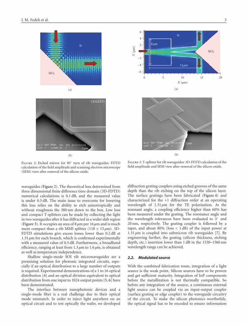
Figure 2: Etched mirror for 90◦ turn of rib waveguides: FDTDcalculation of the field amplitude and scanning electron microscope(SEM) view after removal of the silicon oxide.
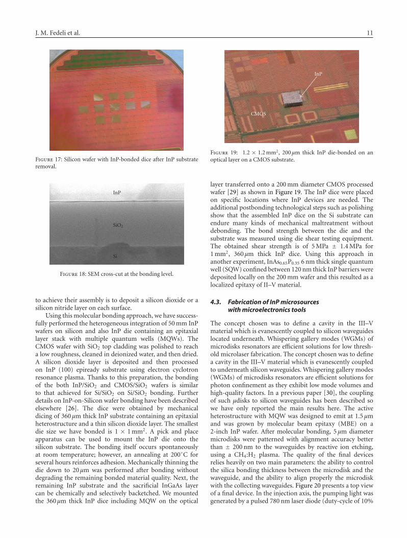
waveguides (Figure 2). The theoretical loss determined fromthree dimensional finite difference time domain (3D-FDTD)numerical calculations is 0.1 dB, and the measured valueis under 0.5 dB. The main issue to overcome for loweringthis loss relies on the ability to etch anisotropically andwithout roughness the 380 nm down to the box. Low lossand compact T-splitters can be made by collecting the lightin two waveguides after it has diffracted in a wider slab region(Figure 3). It occupies an area of 8μm per 16μm and is muchmore compact than a rib MMI splitter (118 × 13μm). 3D-FDTD simulations give excess losses lower than 0.2 dB at1.31μm for each branch, which is confirmed experimentallywith a measured value of 0.5 dB. Furthermore, a broadbandefficiency, ranging at least from 1.3μm to 1.6μm, is obtainedas well as temperature independence.
Shallow single-mode SOI rib microwaveguides are apromising solution for photonic integrated circuits, espe-cially if an optical distribution to a large number of outputsis required. Experimental demonstrations of a 1 to 16 opticaldistribution [4] and an optical division equivalent to opticaldistribution from one input to 1024 output points [5, 6] havebeen demonstrated.
The interface between nanophotonic devices and asingle-mode fiber is a real challenge due to their opticalmode mismatch. In order to inject light anywhere on anoptical circuit and to test optically the wafer, we developed
20151050
X (μm)
−6
−4
−2
0
2
4
6
Y(μ
m)
Si
SiO2
8μm
14μm
(a)
Acc.V16 kV
Spot
3
Magn.
×7500DetSE
WD6
2μm
(b)
Figure 3: T-splitter for rib waveguides: 3D-FDTD calculation of thefield amplitude and SEM view after removal of the silicon oxide.
diffraction grating couplers using etched grooves of the samedepth than the rib etching on the top of the silicon layer.The surface gratings have been fabricated (Figure 4) andcharacterized for the +1 diffraction order at an operatingwavelength of 1.31μm for the TE polarization. At theresonant angle, a coupling efficiency higher than 60% hasbeen measured under the grating. The resonance angle andthe wavelength tolerances have been evaluated to 3◦ and20 nm, respectively. The grating coupler is followed by ataper, and about 80% (loss < 1 dB) of the input power at1.31μm is coupled into submicron rib waveguides [7]. Byengineering further, the grating (silicon thickness, etchingdepth, etc.) insertion lower than 1 dB in the 1530–1560 nmwavelength range can be achieved.
2.2. Modulated source
With the combined fabrication route, integration of a lightsource is the weak point. Silicon sources have to be provenand get sufficient maturity. Integration of InP componentsbefore the metallization is not thermally compatible. Sobefore any integration of the source, a continuous externallight source can be coupled via an input-output coupler(surface grating or edge coupler) to the waveguide circuitryof the circuit. To make the silicon photonics worthwhile,the optical signal has to be encoded to ensure information

4 Advances in Optical Technologies
Si
SiO2
θ
Si substrate
Acc.V15 kV
Spot
3
Magn.
×60000
DetTLD
WD5
Exp
0600 nm
Figure 4: Scanning electron microscope view of a surface 1Dgrating.
transmission at frequencies larger than 10 GHz. Impressiveprogresses have been obtained in the recent years on severalways investigated for high-speed optical modulation in Sior Si-based devices: electro-optical effects in strained silicon[8] or SiGe superlattices [9], quantum confined Stark effectin silicon-germanium/germanium quantum wells [10, 11],Franz Keldysh effect in GeSi diode, [12], carrier concentra-tion variations in silicon [13–18]. The mainly used possibilityto make a high-speed optical modulator is to use indexvariations by free-carrier concentration variations. A lot ofsilicon-based optical modulators made for several years arebased on free-carrier concentration variation using injection,accumulation, or depletion of carriers. Each structure isintegrated in an SOI rib waveguide and the refractive indexvariation induces a phase shift of the guided wave. Aninterference device such as a Mach-Zehnder interferometer,Fabry-Perot microcavity, or microring resonator is used toconvert the phase modulation into an intensity one. The bestpublished results are summarized in Table 1.
For several years, vertical carrier depletion structureshave been proposed by IEF [18, 19], using either SiGe/Simodulation doped quantum wells or all Si structures, placedin the intrinsic region of a PIN diode and integrated in anSOI rib microwaveguide. Holes introduced by thin highly-doped P+ layers in the Si barriers are confined in theintrinsic region of the pin diode at the equilibrium state.When a reverse bias is applied to the diode, the electricalfield sweeps the carriers out of the active region due toband bending. Hole concentration variations are responsiblefor refractive index variations. The intrinsic response timeallows operation at frequencies higher than 10 GHz. The
Boron-doped
Non intentionnaly-dopedMetal
Boron-doped
Oxide Phosphorus-doped
Figure 5: Cross section of the phase shifter structure integrated intoa rib silicon-on-insulator waveguide and optical microscope view ofthe modulator.
performance of the modulators is also dependant on theaccess resistance, in series with the reverse-bias pin diodecapacitor. The challenge is to get low optical losses andlow RC constants in Mach-Zendher or Fabry-Perot interfer-ometer configurations. The variation of the effective indexdue to carrier depletion has been measured at few·10−4 at1.55μm for a 0 V to 6 V reverse voltage bias variation. Afteroptimization of such structure, the obtained factor of merit(Lπ·Vπ) is lower than 1.3. This vertical approach of depletionmodulator was followed recently by Liu et al. [16] and Gardeset al. [17] and the 40 Gb/s operation obtained proves thehigh frequency capacity of the depletion solution. However,the fabricated modulator of this kind requires numerousdoped epitaxy and implantation steps and it would be a realchallenge for a combined fabrication.
So in the aim of reducing the complexity of the fabrica-tion, we proposed hereafter a structure based on a horizontalpin diode which has a simpler technological process withoutany epitaxial steps. The optical loss is reduced as the opticalmode has a weak interaction with the P+ and N+ dopedregions of the diode. A good overlap between the carrierdensity variation zone and the guided mode is obtainedleading to high effective index change. In comparison withvertical diodes [15–18], the capacitance of the diode isreduced, that is favourable to high-speed operation and lowelectrical power dissipation.
A schematic view of the device cross-section is shown inFigure 5. The silicon rib waveguide width is 660 nm, the ribheight is 400 nm, and the etching depth is 100 nm leading toa single mode propagation of the guided mode at 1.55μmwavelength. A P+ doped layer (1018 cm−3) is inserted in theintrinsic region of the pin diode which acts as a source ofholes. The P and N doped regions of the pin diode havedoping concentrations close to 1018 cm−3. Metallic contactsare deposited on both sides of the waveguide, a few micronsapart to reduce optical loss.
The silicon modulator is based on an asymmetric Mach-Zehnder interferometer (Figure 5). The phase shifter isinserted in both arms over a length of 4 mm, and electrodesare used to bias one arm. Waveguide splitters are starcouplers with a reduced area (10 × 2μm2). To ensurehigh-frequency operation, RC time constants have to be

J. M. Fedeli et al. 5
Table 1: State of the art of silicon-based optical modulators.
Modulator type λ (μm)VπLπ Bandwidth or Extinction Insertion
Labs(V·cm) time constant ratio (dB) loss (dB)
Franz Keldysh effectin Ge diode
1.647 no 7.5 2.5S. Jongthammanurak,
Group IV photonics,
ottawa (2006)
Quantum confined Stark1.55 at90◦C
noAbsorptioncoefficientcontrast >3
Kuo and al, IEEE
effect (QCSE) in Ge/SiGe JSTQE, 12 (6)
quantum wells p1503 (2006)
Carrier injection1.55 12.5 Gbit/s >9
Q. Xu et al., Optics express,
in lateral PIN diode 15 (2) p 430 (2007)
MOS capacitance 1.55
7.7 1 GHzA. Liu et al., nature
427, 615–618 (2004)
3.3 10 Gbit/s 3.8 10L. Liao et al.,
optics express 13,
3129–3135 (2005)
Carrier depletion1.55 4 30 GHz
(40 Gbit/s)7
Liu and al optics express,
(vertical PN diode) 15 (2) p660, (2007)
Carrier depletion1.311.55
3.1 (exp)Time constant D. Marris-Morini et al.,
(Doped modulation of ∼ 1ps optics express, 14
vertical Si PIN diode) (Theory) (22) 10838 (2006)
Carrier depletion1.55 5 10 GHz 5 This work(Doped modulation of
all Si lateral PIN diode)
Carrier depletion1.55 3 9 GHz 6 3
T. Pinguet
(Doped modulation of Group IV photonics
all Si lateral PN diode) Tokyo 2007
Carrier depletion1.55
2.5 (theory) Time constant2
F. Y. Gardes et al.,
(four terminal p+pnn+ birefringence <7 ps optics express 13 (22),
vertical device) free (Theory) 8845–8854, (2005)
minimized. The capacitance of the device was evaluatedusing small-signal simulations. The diode capacitance perunit length varies from 2.3 to 1.8·10−16 F/μm for reversebiases from 0 V to −10 V. To ensure operating frequencyabove 10 GHz, the serial resistance of the device should belower than 70Ω/mm. Doped regions and silicide are thusused to form ohmic contacts and to achieve such a lowresistance. Coplanar waveguide electrodes are designed toobtain characteristic impedance around 50 ohms taking intoaccount the capacitance of the pin diode.
The modulator was fabricated on an undoped 200 mmSOI substrate with a 1μm thick buried oxide (BOX) layer,a 400 nm crystalline silicon film, and a 100 nm silica hardmask on top. A 100 nm-wide slit is etched in the hard maskusing 193 nm deep-UV lithographic patterning and reactiveion plasma etching. Double ion implantation and annealingare then performed to obtain a thin slit doped layer onthe whole thickness. Waveguides are patterned with DUVlithography and HBr etching. Implantation for N+ and P+area are performed followed by another annealing. It is worth
to note that these implantation steps could be common to thesource and drain fabrication. Finally, Ti/TiN/AlCu/Ti/TiNmetal stack was deposited onto the wafer and electrodeswere patterned and etched down to the SiO2 layer. The usedprocesses are fully compatible with SOI CMOS technologyand could be transferred in high-volume microelectronicmanufacturing.
The experimental setup uses a tunable laser around1550 nm. A linearly polarized light beam is coupled intothe waveguide using a polarization-maintaining lensed-fiber.The output light is collected by an objective and focused onan IR detector. Electrical probes are used to bias the diode.Very low values of the reverse current (−2μA at −10 V) havebeen measured that ensures low electrical power dissipationin DC configurations. The insertion loss was measured atabout 5 dB. DC extinction ratio is around 14 dB from 0 to−10 V. To evaluate the modulation phase efficiency, a figureof merit is usually defined as the product VπLπ , where Vπ
and Lπ are the applied voltage and the length required toobtain a π phase shift of the guided wave, respectively. The

6 Advances in Optical Technologies
1010.1
Frequency (GHz)
−6
−5
−4
−3
−2
−1
0
Nor
mal
ized
opti
calo
utp
ut
(dB
)
Figure 6: Normalized optical response of the Si modulatorintegrated in rib SOI waveguide with optical 3 dB-bandwidth ofabout 10 GHz.
obtained value VπLπ is equal to 5 V·cm. The normalizedoptical response of the modulator is reported in Figure 6 fora DC bias of −5 V. A 3 dB cutoff frequency of ∼10 GHz ismeasured on a Mach-Zehnder interferometer using 4 mm-long phase shifters.
Several ways improvement can be considered. Designoptimizations of the RF travelling wave and optical waveg-uide are required to increase the modulation bandwidth tosome tens of GHz. Progress in modulation efficiency arealso possible: VπLπ product as low as 1 V·cm is theoreticallypredicted with the proposed structure, thanks to the goodoverlap between the optical mode and the doped regionin the middle of the waveguide where carrier depletionoccurs. The proposed structure has a large potential for therealization of high performances integrated high-speed mod-ulators. Optical loss is reduced as the rib waveguide is notentirely doped, and the reduced-capacitance is favourablefor high speed and low electrical power consumption. Thefabrication can be combined with processing steps of CMOStransistors.
2.3. Germanium photodetectors
High-speed photodetector is one of the key building blocksand a large wavelength range of detection from 850 nmto telecom standards (1.55μm) is necessary. These com-ponents have been available for several years from theIII/V semiconductor technology on InP and GaAs wafers.Nevertheless, the integration of these devices on large waferswithin the mainstream silicon technology requires hybridintegration approach [20, 21]. The used material requireshigh absorption for broadband telecommunication wave-lengths. Within the group IV material, silicon is transparentat the telecommunication wavelengths (λ > 1.2μm) makingit unsuitable for photodetection from 1.31μm to 1.55μm.While pure Germanium is a promising candidate as abroadband photodetector. Furthermore, germanium has adirect energy bandgap of 0.8 eV and is compatible with theCMOS technology.
Despite large lattice mismatch between Ge and Si, whichis about 4.2%, previous works have shown that epitaxialgrowth of high-quality germanium layers on silicon can beachieved using reduced pressure chemical vapor deposition(RP-CVD) or ultrahigh-vacuum chemical vapor deposition(UHV-CVD). The germanium film was grown by RP-CVDon SOI substrates. After the growth of a thin buffer layer(50 nm) at low temperature (400◦C), a Ge layer in the rangeof about 300 nm is typically grown at 700◦C. The first layerenables to avoid three dimensional growths. After a thermalannealing at 750◦C of the stack, the threading dislocationsdensity is in the range of 5·106/cm2. Spectroscopic ellip-sometry measurements confirmed the absence of silicondiffusion as the thickness values of the various layers are closeto the nominal ones.
The measured Ge layer absorption coefficients are closeto 10 000 cm−1 and 5000 cm−1 at 1.31μm and 1.55μm,respectively. The strain-induced Ge bandgap narrowingallows detection to 1.6μm with fairly large internal quantumefficiency. Hall measurements indicated that the layer was P-type, with a hole mobility close to 1300 V·cm−2·s−1 and aresidual carrier density smaller than 1016 cm−3. Pump-probeexperiments using a femtosecond laser have been carriedout and have shown carrier lifetimes much higher thancarrier collection times. Then the recombination rate of thephotogenerated carriers is very low.
Much work has been focused on vertical illuminationGe photodetectors and impressive results with frequencyup to 39 GHz have been obtained [22–24]. We focusedmainly on integrated photodetectors coupled to a siliconrib waveguide. We investigated different technology schemesfor the integration of Ge photodetectors with the siliconrib waveguides described in Section 2.1. The introductionof the germanium absorbing layer has been considered bya direct coupling of the light from the SOI waveguide intogermanium. 3D FDTD simulation shows that in this case95% of the light was absorbed in 4μm length PD (Figure 7)leading to short photodetectors with possible reduced capac-itance in the 10 fF range. However, this increased efficiencyis balanced by the need of etching a recess in the 380 nmthick waveguide. For reliability of the process and due tothe needed tolerance of the partial etching of silicon, therecess was etched with a SiO2 mask to a safe 60 nm ±10 nm thickness. Selective epitaxy was performed and filledthe recess without any cavity between the output of thewaveguide and the germanium layer. A SiO2 cladding wasdeposited after germanium annealing before the fabricationof diodes (Figure 8). Three kinds of diodes have been studied:a metal-Schotkky-metal (MSM), a lateral PIN, and a verticalPIN.
The MSM structure needs an intrinsic Germanium andthe formation of Schottky contacts on the Germanium sur-face. The surface contacts were dry etched in the SiO2 beforeused in microelectronics. I–V curve for different designsshowing the nonlinear behavior of Schottkky contacts wereobtained. The electrode spacing is 1μm. Figure 9 presentsoptical and electron scanning microscope views of the inte-grated photodetector. The measured dark current for such aphotodetector is rather high, that is, 30μA/μm at 6 V. That is

J. M. Fedeli et al. 7
Si
Si
SiO2
Ge
(a)
76543210
Propagation direction (μm)
0
1
2
3
4
Hei
ght
(μm
)
Si
SiO2
SiO2
Ge
(b)
Figure 7: Ge photodetector integrated into a rib silicon-on-insulator waveguide and a 3D-FDTD calculation of the electricfield profile amplitude in a longitudinal cross section of thephotodetector.
Si waveguide
SiO2
WD7
Ge
B164EP10×20 K 1.5μm
Figure 8: RP-CVD germanium epitaxy in a recess at the output ofa silicon rib waveguide.
mainly due to the Schottky barrier height, the dislocationsin Ge layer and the metallic contacts. The responsivityof the 10μm long integrated Ge on Si photodetector isas high as 1 A/W at 1.55μm wavelength [25]. Bandwidthcharacterizations of MSM Ge on Si photodetectors havebeen carried out using two kinds of experimental setupat λ = 1.55μm: time response measurements and opto-RF measurements. The normalized responses at 6V biasobtained for both experiments at 1.55μm, are reported inFigure 10. With opto-RF experiments, the −3 dB bandwidthis close to 25 GHz at 6 V bias. For time response experi-ments, the convolution between a Gaussian profile whichcharacterizes the acquisition system response and a doubleexponential response give an intrinsic response time of the
Side view
SiO2
SiO2(BOX)
Si (substrate)
Si SiGe
DMetalMetal
G208D P09 ×10 K 3μmTilt 20◦
(a)
Top view
Waveguide
10μm
RF electrodes
D
L
(b)
Figure 9: Optical microscope (Top view) and Scanning electronmicroscope (side view) images of the Ge on Si MSM photodetectorintegrated in slightly etched SOI rib waveguide.
Ge on Si photodetector of about 19 picoseconds, whichcorresponds on a cutoff frequency of about 23.5 GHz at 6 Vbias (Figure 10).
The fabrication of vertical PIN photodiode relies onselective epitaxy of in situ P doped layer, followed by intrinsicgermanium and N doped layer. P doping with Boron duringRP-CVD epitaxy was achieved with 1·1019 at/cm3. In situ,N doping epitaxy with a steep profile is a challenge asphosphorus is migrating easily. Deposition of N dopedpolysilicon on top of the intrinsic Ge is an alternative way.However, epitaxy with a high 1.5·1019 at/cm3 doping level,leading to 1.3 mΩ·cm resistivity, has been performed forupper contact of the photodetector. In order to contact the Player at the bottom of the Ge layers, precise etching of Ge forbottom contacting is mandatory for submicron devices. Withan AMAT centura machine using RIE etching with Cl2 gazes,a steep profile (> 80◦) was achieved without any roughness.An SiO2 cladding was then deposited and opened forcontacting the P and N area. The Ti/TiN/AlCu metallizationcompleted the formation of the pads (Figure 11). Depending

8 Advances in Optical Technologies
1007654321076543217654320.1
Frequency (GHz)
−14
−12
−10
−8
−6
−4
−2
0
Nor
mal
ized
resp
onse
(dB
)
2μm1μm0.7μm
Figure 10: Normalized opto-RF responses at 6 V bias obtained forseparation of 2μm (red), 1μm (blue), 0, 7μm (green).
200150100500×10−12
Time
0
0.2
0.4
0.6
0.8
1
Nor
mal
ized
resp
onse Acquisition system
Vp = 0 VVp = 1 VVp = 2 VVp = 3 V
Vp = 4 VVp = 5 VReference
Figure 11: Femtosecond pulse response of an integrated verticalPIN.
of the length of the photodiodes, the dark current is in the nArange. The bandwith exceeded 35 GHz which was the limit ofour test equipment (Figure 11).
2.4. Light generation
As efficient modulators can be performed, a CW light sourceis needed. Different options are followed: light is comingfrom an external InP laser connected with I/O couplersto the passive circuitry of the chip. This required efficientcouplers and expensive packaging. In a second option [2], thelaser source is flip-chipped and the emitted light is collectedvertically via a surface grating coupler. Compared to thefirst option, the packaging is reduced and the integration isincreased. The third option would be to process InP sourceafter transistor fabrication, but it is rather difficult due to
thermal budgets needed for the combined fabrication. TheGraal option would be to process a silicon source. Despite thefact that SiOx-Er layers are a good candidate for such siliconlasers, amplification and lasing have still to be demonstratedin an efficient way. So for a combined fabrication, lightgeneration is really an issue with poor integration.
In conclusion, the results described here above show thata large variety of passive photonic devices except sourcescan be implemented on SOI substrate by means of CMOStechnology. However, as the microelectronic process is verymature, the introduction of a new photonic part in a largeCMOS foundry requires a lot of effort for changing theprocess. Low and medium scale IC foundries are moresuitable to accept such modifications as they can differentiatetheir process and address new markets. However, thiscombined fabrication is fixed for one CMOS technologyand not compatible with other CMOS technologies (SiGe,sSOI, GOI, etc.). As an example, a typical 130 nm CMOStechnology ready for 10 G components may be not suitablefor 40 G devices.
3. SOI PHOTONICS AND CMOS WAFER BONDING
Using the wafer bonding technique, one can introduce aphotonic layer at some level in the processing steps ofCMOS. Since the first metal layers are too densely packedand thin, introduction at the upper metal layers must beconsidered. For example, after the fabrication of metal 4in advanced MOS process, the planarized surface has beencoated with a deposited oxide. On another substrate, aphotonic part is fabricated with silicon waveguides andelectro-optical components. After cladding with oxide andplanarisation of the optical wafer with CMP, perfect cleaningof both wafers facilitates their molecular bonding at roomtemperature. However, one of the flaws with this approachlies in the alignment between the electrical and the photonicparts which today can be as much as ±2μm. Therefore,the design rules for the subsequent metal layers have totake this alignment margin into account. After bonding,grinding and chemical etching of the backside of the Sioptical wafer a flat surface of thermal oxide remains onthe top of the PICMOS circuit. Some subsequent processsteps are needed to electrically connect the electrical andphotonic parts which involve etching through the top layerto contact the electrical circuit below. This technique is oftencalled 3D heterogeneous integration because the CMOS partis separated from the photonic part without any siliconsurface waste at the transistor level. With this approach, anymicroelectronics technologies can be used for the electricalparts and III–V components can be embedded in thephotonic layer.
We have performed two demonstrations of this conceptin collaboration with TRACIT Technology. On SOITECoptical SOI, we have processed a silicon rib network withcavities filled with Ge. After an SiO2 cladding deposition, theoptical wafer was carefully polished and bonded to a CMOSwafer before substrate removal (Figure 13). An SEM cross-cut observation revealed no interface between the two SiO2

J. M. Fedeli et al. 9
Si rib waveguide
Top contact
GermaniumBOX
Silicon substrate
G208E P04LETI ×7 K 4.29μm
Figure 12: SEM view of a PIN vertical PD.
Corner mirror
Splitter
Ge cavity
Figure 13: Rib waveguides with splitters, corner mirrors, rectangu-lar cavities filled with germanium on a CMOS at level M4.
layers and no degradation of either the metal or the photoniclayers (Figure 14).
This wafer bonding technique is a very promising wayto integrate a photonic layer into a CMOS technology. Thewafer bonding technique is mature and the intraconnections(3D techniques) are well addressed by the electronicscommunity. The PIC can use all the components for thecombined fabrication and integrate InP sources by dieto wafer bonding. The EIC can use any new electronicstechnology and can be tested before the wafer bonding aswell as the PIC. However, the main challenge that needs tobe faced is the bonding cost issue compared to the combinedfabrication.
4. HETEROGENEOUS INTEGRATION
As long as temperature is constrained so that it must notexceed 400◦C, a photonic layer can be defined above thetransistors and the dielectric/metallic levels. The obviousway to introduce such a photonic layer is to treat it as an
Silicon
Ge cavity
SiO2
Metallizations
×15 K 2μm
Figure 14: Cross-cut of a CMOS wafer with metal levels and abonded photonic layer with rib waveguides and rectangular cavitiesfilled with germanium.
additional metallic layer on top of most of the layers thathave been used for the electrical interconnect. For the passivecircuitry, we developed hydrogneited amorphous siliconlayer which have a high contrast index. For the active parts,such as the introduction of copper for electrical interconnect,new materials like low temperature III–V compounds canbe introduced on the wafers in a dedicated part of theCMOS clean room. After a CMP planarization and surfacepreparation, QD or MQW layers on top of an InP substrateare bonded on the wafers without precise alignment tofabricated aSi waveguides. The InP substrate of these die isthen removed by chemical etching and further processingsteps are performed which lead to sources and detectorsconnected to the metallic interconnects of the integratedcircuit.
4.1. Amorphous silicon waveguide fabrication
As the area of a CMOS circuit can range from 1 cm2 to2 cm2, increasing the refractive index contrast between thecladding and the guiding medium leads to more compactdevices. With silicon oxide and silicon films, this is achievedwith a value of 2, however, the losses have to be mini-mized. As with monocrystalline silicon on SOI, the highindex difference allows the simultaneous use of refractivecompact components and photonic crystal componentsfor wavelength functionality. Amorphous silicon films weredeposited by a capacitively coupled plasma reactor, with anRF excitation frequency (13.56 MHz). The power can betuned from 30 to 1200 W and the operating pressure can bevaried from 0.2 mtorr to few torr. All films were depositedat temperatures lower than 400◦C to avoid damage to theinterconnect layers. TEOS was used as precursor for oxidedeposition and silane/H2 mixture for the amorphous silicon.Sheet optical guided losses at the full after level duringprocess were measured using a prism coupling technique(METRICON 5010) at 1.3μm and 1.55μm. By optimizingthe H2/Silane ratio in the deposition chamber, silicon filmswith losses as low as 0.2 dB/cm at 1.55μm after 350◦Cannealing were deposited on silicon wafers covered with

10 Advances in Optical Technologies
1μm TEOS. DUV 193 nm or 248 nm lithography with orwithout hard mask and HBr silicon etching were usedto define the waveguide and basic passive functions foroptical links (Figure 15). A thick 1μm SiO2 TEOS oxidewas deposited to provide an upper cladding. Measurementswere performed at a spectral range between 1.25 to 1.65μm.Results are compared to previous SOI waveguides data[26]. The propagation losses decrease when the width ofthe waveguide increases and for a guide of width 500 nm(limits to have a monomode waveguide), there is only adip towards the wavelength of 1380 nm. The losses arecomparable to that of an SOI waveguide. We can notice thatfor this a:Si waveguide, the losses are, respectively, equal to5 and 4 dB/cm for the wavelengths of 1300 and 1550 nm.We can consider that these losses are essentially due to thediffraction phenomenon due to the side wall roughness ofthe waveguide. For the waveguide of 800 nm width, the lossesbecome very weak, lower than one dB/cm for wavelengthsclose to 1300 nm, and tend toward the values of a planarwaveguide for both types of waveguides (with or withoutthermal annealing of 350◦C), this shows that the materialhas a good stability in time. Experimental results of thebasic building blocks obtain on the amorphous silicon arein a good agreement with those of the SOI technology.The μbends of 2μm radius exhibited only negligible losses(0.04 dB/μbend) for all the spectral range. Measurements ona very compact size of 2 × 4.2μm2 MMI devices give anextra losses of 1 dB at λ = 1.3μm (the design wavelength),a spectral range at 1 dB of 500 nm and the imbalance
between the two output is lower than 0.5 dB for all thespectral range. The most important features for amorphoussilicon circuitry is the easy possibility to pile up layers and,therefore, to open new designs concepts or to ease designssuch as crossings or coupling. As an example, in Figure 16, aaSi surface gratings is formed on top a aSi/SiO2 Bragg mirrorsfor an increase in the coupling efficiency with a fiber.
4.2. Die to wafer bonding of InP sources
Even with the latest development on active silicon photonics,III–V components remain more efficient for light-matterinteraction. However, the cost of wafers and processing onsmall diameter wafers leads to rather expensive components.Integration of InP components coupled to passive opticalfunctions on top of a CMOS requires a new approach whichis different from the flip-chip solution. The first issue wouldbe to enable integration of InP-based laser heterostructureson top of an IC. Another objective was to be able to processthe InP-based components in the same way as the CMOStransistors in order to reduce the cost of the introduc-tion of III–V components. As passive components can beefficiently developed with SiN or Si technology, only theactive components require an InP technology. One shouldnote that photonic sources or other active devices shouldexhibit low power consumption, and a small footprint, andshould also operate at high speed. For all of these reasons,the needed devices should be as small and integrated aspossible. This means that the InP-based components occupya very small surface on a large CMOS circuit. Therefore,
aSi:H waveguide
aSi:H disk
×25 K 1.2μm
Figure 15: Amorphous Si waveguide with resonating disk.
aSi:H grating
aSi/SiO2 Bragg mirror
Si bulk
SiO2
L994P-P16
×11 K 2.73μm
Figure 16: Cross-cut of an amorphous Si gratings on top of a Braggmirror made of an:Si/SiO2 alternate layers.
our approach consists of dicing an InP wafer with all theheteroepitaxial layers, bonding the die to the required places,removing the back of the InP die in order to only leave theactive thin films attached to the CMOS wafer, thus enablingprocessing of InP components on a dedicated 200 or 300 mmfabrication line. To mount the die, molecular bonding wasselected because good bonding quality can be achievedwithout any additional adhesive materials [22, 23]. In fact,the presence of the bonding material could inhibit efficientoptical coupling. Furthermore, molecular bonding satisfiesthe requirements better in term of thermal conductivity anddissipation, transparency at the device working wavelengthsand mechanical resistance.
Surface morphology and chemistry are critical to thebonding quality. Prior to bonding the die, the surfaces mustbe flat and uniform. The required flatness and uniformitycan be obtained by use of CMP. The additional role of CMPpolishing is to adjust the thickness of the silicon dioxidecladding layer in order to satisfy the optical coupling con-ditions. The surfaces were carefully cleaned and hydrated inthe chemical solution and bonding can occur spontaneouslywhen the prepared wafers are made of silicon. A completephysical model of such a molecular bonding was proposedand presented by Stengl et al. [27] and Gosele et al. [28].As these materials are of dissimilar nature, one possible way
J. M. Fedeli et al. 11
Figure 17: Silicon wafer with InP-bonded dice after InP substrateremoval.
InP
SiO2
Si
Figure 18: SEM cross-cut at the bonding level.
to achieve their assembly is to deposit a silicon dioxide or asilicon nitride layer on each surface.
Using this molecular bonding approach, we have success-fully performed the heterogeneous integration of 50 mm InPwafers on silicon and also InP die containing an epitaxiallayer stack with multiple quantum wells (MQWs). TheCMOS wafer with SiO2 top cladding was polished to reacha low roughness, cleaned in deionized water, and then dried.A silicon dioxide layer is deposited and then processedon InP (100) epiready substrate using electron cyclotronresonance plasma. Thanks to this preparation, the bondingof the both InP/SiO2 and CMOS/SiO2 wafers is similarto that achieved for Si/SiO2 on Si/SiO2 bonding. Furtherdetails on InP-on-Silicon wafer bonding have been describedelsewhere [26]. The dice were obtained by mechanicaldicing of 360μm thick InP substrate containing an epitaxialheterostructure and a thin silicon dioxide layer. The smallestdie size we have bonded is 1 × 1 mm2. A pick and placeapparatus can be used to mount the InP die onto thesilicon substrate. The bonding itself occurs spontaneouslyat room temperature; however, an annealing at 200◦C forseveral hours reinforces adhesion. Mechanically thinning thedie down to 20μm was performed after bonding withoutdegrading the remaining bonded material quality. Next, theremaining InP substrate and the sacrificial InGaAs layercan be chemically and selectively backetched. We mountedthe 360μm thick InP dice including MQW on the optical
InP
CMOS
Figure 19: 1.2 × 1.2 mm2, 200μm thick InP die-bonded on anoptical layer on a CMOS substrate.
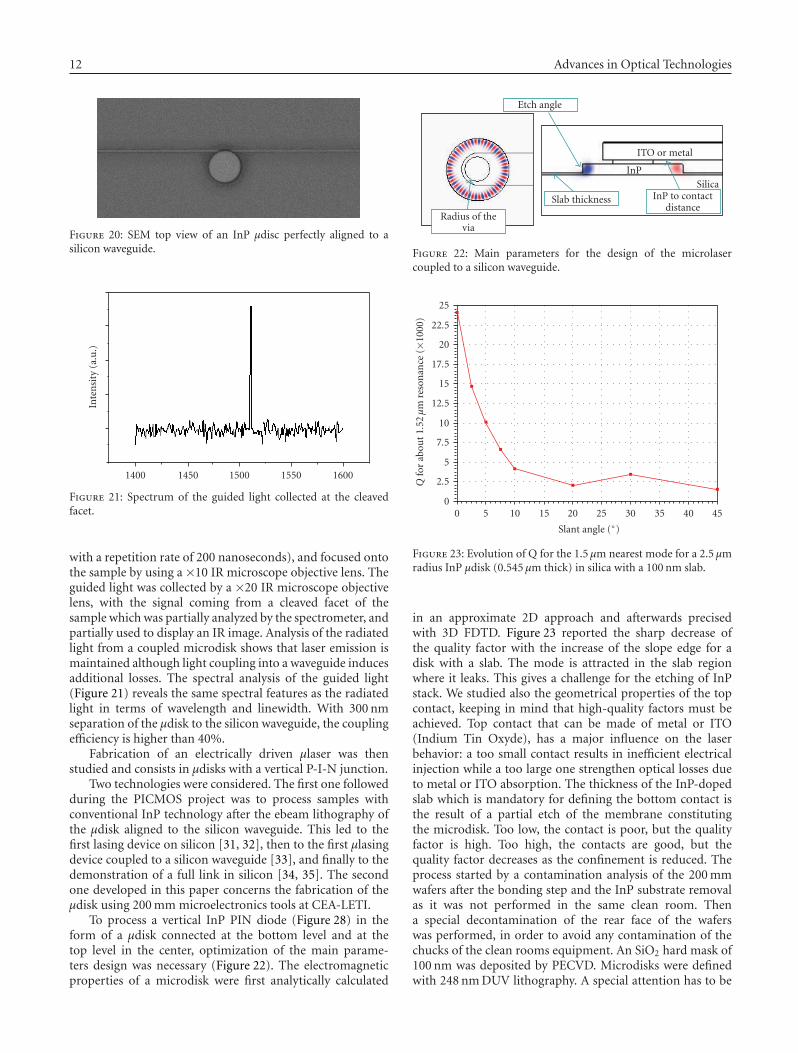
layer transferred onto a 200 mm diameter CMOS processedwafer [29] as shown in Figure 19. The InP dice were placedon specific locations where InP devices are needed. Theadditional postbonding technological steps such as polishingshow that the assembled InP dice on the Si substrate canendure many kinds of mechanical maltreatment withoutdebonding. The bond strength between the die and thesubstrate was measured using die shear testing equipment.The obtained shear strength is of 5 MPa ± 1.4 MPa for1 mm2, 360μm thick InP dice. Using this approach inanother experiment, InAs0.65P0.35 6 nm thick single quantumwell (SQW) confined between 120 nm thick InP barriers weredeposited locally on the 200 mm wafer and this resulted as alocalized epitaxy of II–V material.
4.3. Fabrication of InP microsourceswith microelectronics tools
The concept chosen was to define a cavity in the III–Vmaterial which is evanescently coupled to silicon waveguideslocated underneath. Whispering gallery modes (WGMs) ofmicrodisks resonators are efficient solutions for low thresh-old microlaser fabrication. The concept chosen was to definea cavity in the III–V material which is evanescently coupledto underneath silicon waveguides. Whispering gallery modes(WGMs) of microdisks resonators are efficient solutions forphoton confinement as they exhibit low mode volumes andhigh-quality factors. In a previous paper [30], the couplingof such μdisks to silicon waveguides has been described sowe have only reported the main results here. The activeheterostructure with MQW was designed to emit at 1.5 μmand was grown by molecular beam epitaxy (MBE) on a2-inch InP wafer. After molecular bonding, 5 μm diametermicrodisks were patterned with alignment accuracy betterthan ± 200 nm to the waveguides by reactive ion etching,using a CH4:H2 plasma. The quality of the final devicesrelies heavily on two main parameters: the ability to controlthe silica bonding thickness between the microdisk and thewaveguide, and the ability to align properly the microdiskwith the collecting waveguides. Figure 20 presents a top viewof a final device. In the injection axis, the pumping light wasgenerated by a pulsed 780 nm laser diode (duty-cycle of 10%
12 Advances in Optical Technologies
Figure 20: SEM top view of an InP μdisc perfectly aligned to asilicon waveguide.
16001550150014501400
Inte
nsi
ty(a
.u.)
Figure 21: Spectrum of the guided light collected at the cleavedfacet.
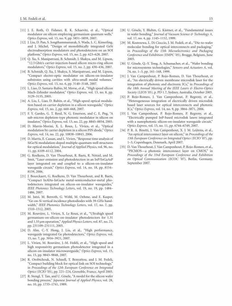
with a repetition rate of 200 nanoseconds), and focused ontothe sample by using a ×10 IR microscope objective lens. Theguided light was collected by a ×20 IR microscope objectivelens, with the signal coming from a cleaved facet of thesample which was partially analyzed by the spectrometer, andpartially used to display an IR image. Analysis of the radiatedlight from a coupled microdisk shows that laser emission ismaintained although light coupling into a waveguide inducesadditional losses. The spectral analysis of the guided light(Figure 21) reveals the same spectral features as the radiatedlight in terms of wavelength and linewidth. With 300 nmseparation of the μdisk to the silicon waveguide, the couplingefficiency is higher than 40%.
Fabrication of an electrically driven μlaser was thenstudied and consists in μdisks with a vertical P-I-N junction.
Two technologies were considered. The first one followedduring the PICMOS project was to process samples withconventional InP technology after the ebeam lithography ofthe μdisk aligned to the silicon waveguide. This led to thefirst lasing device on silicon [31, 32], then to the first μlasingdevice coupled to a silicon waveguide [33], and finally to thedemonstration of a full link in silicon [34, 35]. The secondone developed in this paper concerns the fabrication of theμdisk using 200 mm microelectronics tools at CEA-LETI.
To process a vertical InP PIN diode (Figure 28) in theform of a μdisk connected at the bottom level and at thetop level in the center, optimization of the main parame-ters design was necessary (Figure 22). The electromagneticproperties of a microdisk were first analytically calculated
Etch angle
InP to contactdistance
ITO or metal
InP
Slab thickness
Silica
Radius of thevia
Figure 22: Main parameters for the design of the microlasercoupled to a silicon waveguide.
454035302520151050
Slant angle (◦)
0
2.5
5
7.5
10
12.5
15
17.5
20
22.5
25
Qfo
rab
out
1.52μ
mre
son
ance
(×10
00)
Figure 23: Evolution of Q for the 1.5 μm nearest mode for a 2.5 μmradius InP μdisk (0.545 μm thick) in silica with a 100 nm slab.
in an approximate 2D approach and afterwards precisedwith 3D FDTD. Figure 23 reported the sharp decrease ofthe quality factor with the increase of the slope edge for adisk with a slab. The mode is attracted in the slab regionwhere it leaks. This gives a challenge for the etching of InPstack. We studied also the geometrical properties of the topcontact, keeping in mind that high-quality factors must beachieved. Top contact that can be made of metal or ITO(Indium Tin Oxyde), has a major influence on the laserbehavior: a too small contact results in inefficient electricalinjection while a too large one strengthen optical losses dueto metal or ITO absorption. The thickness of the InP-dopedslab which is mandatory for defining the bottom contact isthe result of a partial etch of the membrane constitutingthe microdisk. Too low, the contact is poor, but the qualityfactor is high. Too high, the contacts are good, but thequality factor decreases as the confinement is reduced. Theprocess started by a contamination analysis of the 200 mmwafers after the bonding step and the InP substrate removalas it was not performed in the same clean room. Thena special decontamination of the rear face of the waferswas performed, in order to avoid any contamination of thechucks of the clean rooms equipment. An SiO2 hard mask of100 nm was deposited by PECVD. Microdisks were definedwith 248 nm DUV lithography. A special attention has to be

J. M. Fedeli et al. 13
Ti/TiN/AlCubottom contact
Ti/TiN/AlCutop contact InP μ disk
InP bottom layer
Figure 24: Optical top view of a micro disk.
made on the focus, due to the presence of the dice on limitedarea of the wafer. The hard mask is then etched with InPas stopping layer. The partial etching was performed withICP equipment using HBr reactive ion etching. A secondlithography step followed by an InP etching defined theslab necessary for the bottom contact. Then 1.5 μm SiO2
TEOS, that is, a low index and electrical isolating material,was deposited in place of the BCB used for planarization inthe PICMOS demonstration. Chemical mechanical polishing(CMP) was then performed to get a planar surface with400 nm separation with the upper surface of the InP disk.This distance between the membrane, where modes arepropagating and the absorbing contacts were optimized forITO contacts to get the highest Q. However, higher valuecould be useful with more absorbing material. As the Pcontact requires very high doping, which increases opticalabsorption, the studied structures use a tunnel junction toget two N contacts. Even if gold-based contacts have wellknown properties on InP, CMOS processes are not compat-ible with such a metal (except for back-end metallization)because of contamination risks. Ti/TiN/AlCu contacts werean alternative solution since we can get a low resistivecontact. TLM measurements were performed on a trial InPwafer with a 500 nm thick 5·1018 cm−3 N+Si doped layerand showed that the contacts were ohmic types. So top andbottom electrodes were formed by openings the SiO2 to thebottom and upper InP N-doped surface and by patterningthe electrodes after the Ti/TiN/AlCu deposition. Figure 24shows the final device. Light emission in continuous wave(CW) electrical injection at room temperature was observed,but optical characterization proved that no structure waslasing, even in pulsed mode. The electrical threshold wasdetermined to 0.7 V. Emitting light is possible under electricpower as high as 150 mW, without reducing too much thelight power. Maximum light emission is obtained at 30 mW.Lateral roughness and the etching slant are two criticalparameters to get efficient resonators. Considering the realslab thickness that was 400 nm for a membrane of 1 μm,FDTD proved that these first samples with 45◦ slanted edgescould not get higher quality factors than 500 what is too lowto reach lasing mode.
Some devices with large area were tested as photode-tectors (Figure 28), even their shapes did not match with abeam coming from a fiber vertically to the substrate. With
1.510.50−0.5−1
Voltage (V)
0.0
0.2
0.4
0.6
0.8
1.0
1.2
1.4
1.6
1.8
2.0
2.2
2.4
2.6
Cu
rren
t(k
A/c
m2)
Figure 25: PIN characteristic for Ti/TiN/AlCu contacts.
302826242220181614121086420
Current (mA)
0
0.1
0.2
0.3
0.4
0.5
0.6
0.7
0.8
0.9
1Li
ght
pow
er(a
.u.)
0
0.5
1
1.5
2
2.5
3
3.5
4
4.5
5
Vol
tage
(V)
Figure 26: Light power emission at room temperature (in blue) andvoltage (in red).
the cross-cut of Figure 27, the TiAlCu were contacted withP and N-type layers, giving a PIN diode without the tunneljunction. The dark current at −1 V was quite low (1 nA) fora surface of 900μm2. This low value can be explained bypassivation of the slanted edges with HBr etching. With asurface illumination at 1.55μm, the sensitivity was measuredin the range of 10 mA/W. This resulted from the very thinabsorption layer. So by changing the active layers to moreabsorbing ones like InGasAs with a thickness up to 1μm, thesensitivity can be largely improved to the A/W range, whilekeeping low dark current. So, arrays of III–V photodetectorscan be processed on 200 mm wafers with microelectronics’tools.
Therefore, basic elementary building blocks for thedemonstration of a laser source coupled to a siliconwaveguide and photodetectors have been demonstrated andfabrication is possible on a 200 mm Si fabrication line.However, more studies such as optimization of the etchingprocess, investigations of temperature dependency, power

14 Advances in Optical Technologies
InP N + 2E18
InAsP QW
InP P+ 5E17
TJ P++/N++
InP N+ 2E18
259 nm
331 nm
1.014μm
244 nm
51 nm
119 nm
431 nm
×80 K 375 nm
Figure 27: SEM slice view of a micro disk.
Figure 28: Hexagon used for photodetection.
range, and so on have to be performed before they can beused in applications.
5. CONCLUSION
Several different approaches for making the integration ofa photonic layer on a CMOS circuit have been reported:the hybridization of photonics on top of a CMOS, acombined fabrication at the front end level, the waferbonding of SOI photonic circuit at the back-end level, andan embedded photonic layer between metallization have allbeen performed and some results have been presented. Thesedifferent approaches lead to different technologies with theirown merits and drawbacks. Depending of the applicationsand the associated volumes of fabrication, the systemdesigners would be able to choose the best way to make theirdesired system if the necessary building blocks were available.We have presented for each approach some technology routesto the achievement of these building blocks: for combinedfabrication, a silicon rib technology was developed with low0.1 dB/cm losses, 35 GHz Ge photodetectors, and 10 GHz Simodulators. A wafer bonding of an SOI wafer with siliconrib waveguide and cavities filled with Ge or with photoniccrystals was achieved above metallization of a CMOS wafer.With the back-end level approach, direct fabrication of aphotonic layer was achieved with low-temperature processes.
Low-temperature waveguide technologies with amorphoussilicon (loss 5 dB/cm) were developed. The molecular bond-ing of InP dice and the fabrication of InP microdisks usingmicroelectronics tools base demonstrate that III–V μsourcescan be developed on silicon substrates. A 40% coupling wasachieved to a stripe silicon waveguide, but only LED modewas demonstrated with electrical injection, due to poor InPetching. Clearly, the improvement and development of suchphotonics building blocks need to be carried on for thedevelopment of photonic integrated CMOS chip (PICMOS).
ACKNOWLEDGMENTS
This paper summarizes the work of numerous other fellowswho could not be all cited and the authors wanted toacknowledge them. The CMOS wafers used for technologydemonstration were provided by STMicroelectronics. Thiswork is supported by the European community projectsFP6-2002-IST-1-002131-PICMOS and FP6-RII3-CT-2004-50623 MNTEurope and by the French RMNT programs“CAURICO” and “HETEROPT.” The authors thank SuzanneLaval, Eric Cassan, Paul Crozat, and Juliette Mangeney fromIEF for fruitful discussions. They also acknowledge the staffof the 200 mm clean rooms of the LETI for the fabrication ofhigh-quality optical structures.
REFERENCES
[1] G. T. Reed, “The optical age of silicon,” Nature, vol. 427, no.6975, pp. 595–596, 2004.
[2] G. Nunn, “CMOS photonics,” in Proceedings of the IEEE SOIConference (SOI ’06), Niagara Falls, NY, USA, October 2006.
[3] S. Lardenois, D. Pascal, L. Vivien, et al., “Low-loss submicrom-eter silicon-on-insulator rib waveguides and corner mirrors,”Optics Letters, vol. 28, no. 13, pp. 1150–1152, 2003.
[4] L. Vivien, S. Lardenois, D. Pascal, et al., “Experimental demon-stration of a low-loss optical H-tree distribution using silicon-on-insulator microwaveguides,” Applied Physics Letters, vol.85, no. 5, pp. 701–703, 2004.
[5] D. Marris, L. Vivien, D. Pascal, et al., “Experimental demon-stration of 1 to 1024 optical division using slightly etchedrib silicon-on-insulator waveguides,” in Proceedings of the 2ndIEEE International Conference on Group IV Photonics, pp. 204–206, Antwerp, Belgium, September 2005.
[6] D. Marris, L. Vivien, D. Pascal, et al., “Ultralow loss suc-cessive divisions using silicon-on-insulator microwaveguides,”Applied Physics Letters, vol. 87, no. 21, Article ID 211102, 3pages, 2005.
[7] L. Vivien, D. Pascal, S. Lardenois, et al., “Light injection inSOI microwaveguides using high-efficiency grating couplers,”Journal of Lightwave Technology, vol. 24, no. 10, pp. 3810–3815, 2006.
[8] R. S. Jacobsen, K. N. Andersen, P. I. Borel, et al., “Strainedsilicon as a new electro-optic material,” Nature, vol. 441, no.7090, pp. 199–202, 2006.
[9] P. Yu, J. Wu, and B.-F. Zhu, “Enhanced quantum-confinedPockels effect in SiGe superlattices,” Physical Review B, vol. 73,Article ID 235328, 7 pages, 2006.
[10] Y.-H. Kuo, Y. K. Lee, Y. Ge, et al., “Strong quantum-confined Stark effect in germanium quantum-well structureson silicon,” Nature, vol. 437, no. 7063, pp. 1334–1336, 2005.
J. M. Fedeli et al. 15
[11] J. E. Roth, O. Fidaner, R. K. Schaevitz, et al., “Opticalmodulator on silicon employing germanium quantum wells,”Optics Express, vol. 15, no. 9, pp. 5851–5859, 2007.
[12] J. Liu, D. Pan, S. Jongthammanurak, S. Wada, L. C. Kimerling,and J. Michel, “Design of monolithically integrated GeSielectroabsorption modulators and photodetectors on an SOIplatform,” Optics Express, vol. 15, no. 2, pp. 623–628, 2007.
[13] Q. Xu, S. Manipatruni, B. Schmidt, J. Shakya, and M. Lipson,“12.5 Gbit/s carrier-injection-based silicon micro-ring siliconmodulators,” Optics Express, vol. 15, no. 2, pp. 430–436, 2007.
[14] B. Schmidt, Q. Xu, J. Shakya, S. Manipatruni, and M. Lipson,“Compact electro-optic modulator on silicon-on-insulatorsubstrates using cavities with ultra-small modal volumes,”Optics Express, vol. 15, no. 6, pp. 3140–3148, 2007.
[15] L. Liao, D. Samara-Rubio, M. Morse, et al., “High speed siliconMach-Zehnder modulator,” Optics Express, vol. 13, no. 8, pp.3129–3135, 2005.
[16] A. Liu, L. Liao, D. Rubin, et al., “High-speed optical modula-tion based on carrier depletion in a silicon waveguide,” OpticsExpress, vol. 15, no. 2, pp. 660–668, 2007.
[17] F. Y. Gardes, G. T. Reed, N. G. Emerson, and C. E. Png, “Asub-micron depletion-type photonic modulator in silicon oninsulator,” Optics Express, vol. 13, no. 22, pp. 8845–8854, 2005.
[18] D. Marris-Morini, X. L. Roux, L. Vivien, et al., “Opticalmodulation by carrier depletion in a silicon PIN diode,” OpticsExpress, vol. 14, no. 22, pp. 10838–10843, 2006.
[19] D. Marris, E. Cassan, and L. Vivien, “Response time analysis ofSiGe/Si modulation-doped multiple-quantum-well structuresfor optical modulation,” Journal of Applied Physics, vol. 96, no.11, pp. 6109–6112, 2004.
[20] G. Roelkens, D. Van Thourhout, R. Baets, R. Notzel, and M.Smit, “Laser emission and photodetection in an InP/InGaAsPlayer integrated on and coupled to a silicon-on-insulatorwaveguide circuit,” Optics Express, vol. 14, no. 18, pp. 8154–8159, 2006.
[21] J. Bourckaert, G. Roelkens, D. Van Thourhout, and R. Baets,“Compact InAlAs-InGaAs metal-semiconductor-metal pho-todetectors integrated on silicon-on-insulator waveguides,”IEEE Photonics Technology Letters, vol. 19, no. 19, pp. 1484–1486, 2007.
[22] M. Jutzi, M. Berroth, G. Wohl, M. Oehme, and E. Kasper,“Ge-on-Si vertical incidence photodiodes with 39-GHz band-width,” IEEE Photonics Technology Letters, vol. 17, no. 7, pp.1510–1512, 2005.
[23] M. Rouviere, L. Vivien, X. Le Roux, et al., “Ultrahigh speedgermanium-on-silicon-on-insulator photodetectors for 1.31and 1.55 μm operation,” Applied Physics Letters, vol. 87, no. 23,pp. 231109–231111, 2005.
[24] D. Ahn, C.-Y. Hong, J. Liu, et al., “High performance,waveguide integrated Ge photodetectors,” Optics Express, vol.15, no. 7, pp. 3916–3921, 2007.
[25] L. Vivien, M. Rouviere, J.-M. Fedeli, et al., “High speed andhigh responsivity germanium photodetector integrated in asilicon-on-insulator microwaveguide,” Optics Express, vol. 15,no. 15, pp. 9843–9848, 2007.
[26] R. Orobtchouk, N. Schnell, T. Benyattou, and J. M. Fedeli,“Compact building block for optical link on SOI technology,”in Proceedings of the 12th European Conference on IntegratedOptics (ECIO ’05), pp. 221–224, Grenoble, France, April 2005.
[27] R. Stengl, T. Tan, and U. Gosele, “A model for the silicon waferbonding process,” Japanese Journal of Applied Physics, vol. 28,no. 10, pp. 1735–1741, 1989.
[28] U. Gosele, Y. Bluhm, G. Kastner, et al., “Fundamental issuesin wafer bonding,” Journal of Vacuum Science & Technology A,vol. 17, no. 4, pp. 1145–1152, 1999.
[29] M. Kostrzewa, L. Di Cioccio, J. M. Fedeli, et al., “Die-to-wafermolecular bonding for optical interconnects and packaging,”in Proceedings of the 15th Microelectronics and PackagingConference and Exhibition (EMPC ’05), Brugge, Belgium, June2005.
[30] U. Gosele, Q.-Y. Tong, A. Schumacher, et al., “Wafer bondingfor microsystems technologies,” Sensors and Actuators A, vol.74, no. 1–3, pp. 161–168, 1999.
[31] J. Van Campenhout, P. Rojo-Romeo, D. Van Thourhout, etal., “An electrically driven membrane microdisk laser for theintegration of photonic and electronic ICs,” in Proceedings ofthe 18th Annual Meeting of the IEEE Lasers & Electro-OpticsSociety (LEOS ’05), p. PD 1.7, Sydney, Australia, October 2005.
[32] P. Rojo-Romeo, J. Van Campenhout, P. Regreny, et al.,“Heterogeneous integration of electrically driven microdiskbased laser sources for optical interconnects and photonicICs,” Optics Express, vol. 14, no. 9, pp. 3864–3871, 2006.
[33] J. Van Campenhout, P. Rojo-Romeo, P. Regreny, et al.,“Electrically pumped InP-based microdisk lasers integratedwith a nanophotonic silicon-on-insulator waveguide circuit,”Optics Express, vol. 15, no. 11, pp. 6744–6749, 2007.
[34] P. R. A. Binetti, J. Van Campenhout, X. J. M. Leijtens, et al.,“An optical interconnect layer on silicon,” in Proceedings of the13th European Conference on Integrated Optics (ECIO ’07), pp.1–3, Copenhagen, Denmark, April 2007.
[35] D. Van Thourhout, J. Van Campenhout, P. Rojo-Romeo, et al.,“PICMOS—a photonic interconnect layer on CMOS,” inProceedings of the 33rd European Conference and Exhibitionon Optical Communication (ECOC ’07), Berlin, Germany,September 2007.

International Journal of
AerospaceEngineeringHindawi Publishing Corporationhttp://www.hindawi.com Volume 2010
RoboticsJournal of
Hindawi Publishing Corporationhttp://www.hindawi.com Volume 2014
Hindawi Publishing Corporationhttp://www.hindawi.com Volume 2014
Active and Passive Electronic Components
Control Scienceand Engineering
Journal of
Hindawi Publishing Corporationhttp://www.hindawi.com Volume 2014
International Journal of
RotatingMachinery
Hindawi Publishing Corporationhttp://www.hindawi.com Volume 2014
Hindawi Publishing Corporation http://www.hindawi.com
Journal ofEngineeringVolume 2014
Submit your manuscripts athttp://www.hindawi.com
VLSI Design
Hindawi Publishing Corporationhttp://www.hindawi.com Volume 2014
Hindawi Publishing Corporationhttp://www.hindawi.com Volume 2014
Shock and Vibration
Hindawi Publishing Corporationhttp://www.hindawi.com Volume 2014
Civil EngineeringAdvances in
Acoustics and VibrationAdvances in
Hindawi Publishing Corporationhttp://www.hindawi.com Volume 2014
Hindawi Publishing Corporationhttp://www.hindawi.com Volume 2014
Electrical and Computer Engineering
Journal of
Advances inOptoElectronics
Hindawi Publishing Corporation http://www.hindawi.com
Volume 2014
The Scientific World JournalHindawi Publishing Corporation http://www.hindawi.com Volume 2014
SensorsJournal of
Hindawi Publishing Corporationhttp://www.hindawi.com Volume 2014
Modelling & Simulation in EngineeringHindawi Publishing Corporation http://www.hindawi.com Volume 2014
Hindawi Publishing Corporationhttp://www.hindawi.com Volume 2014
Chemical EngineeringInternational Journal of Antennas and
Propagation
International Journal of
Hindawi Publishing Corporationhttp://www.hindawi.com Volume 2014
Hindawi Publishing Corporationhttp://www.hindawi.com Volume 2014
Navigation and Observation
International Journal of
Hindawi Publishing Corporationhttp://www.hindawi.com Volume 2014
DistributedSensor Networks
International Journal of