dft123
TRANSCRIPT
How does Scan Work? Prepared by Mahmut Yilmaz
Scan Chain Operation for Stuckat Test
Design Under Test (DUT)
Combinatio
nal Logic
Combinatio
nal Logic
Combinatio
nal Logic
Combinatio
nal Logic
Scan Enable
Prim
ary Outpu
ts (P
O)
Prim
ary Inpu
ts (P
I)
Scan Out
Scan In
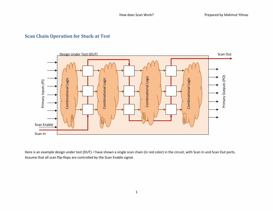
Here is an example design under test (DUT). I have shown a single scan chain (in red color) in the circuit, with Scan In and Scan Out ports. Assume that all scan flip‐flops are controlled by the Scan Enable signal.
1
How does Scan Work? Prepared by Mahmut Yilmaz
Design Under Test (DUT)
Combinatio
nal Logic
X
X
X
Combinatio
nal Logic
X
X
X
X
X
X
Combinatio
nal Logic
Combinatio
nal Logic
Scan Enable=1
Prim
ary Outpu
ts (P
O)
Prim
ary Inpu
ts (P
I)
Scan Out
Scan In 100101011
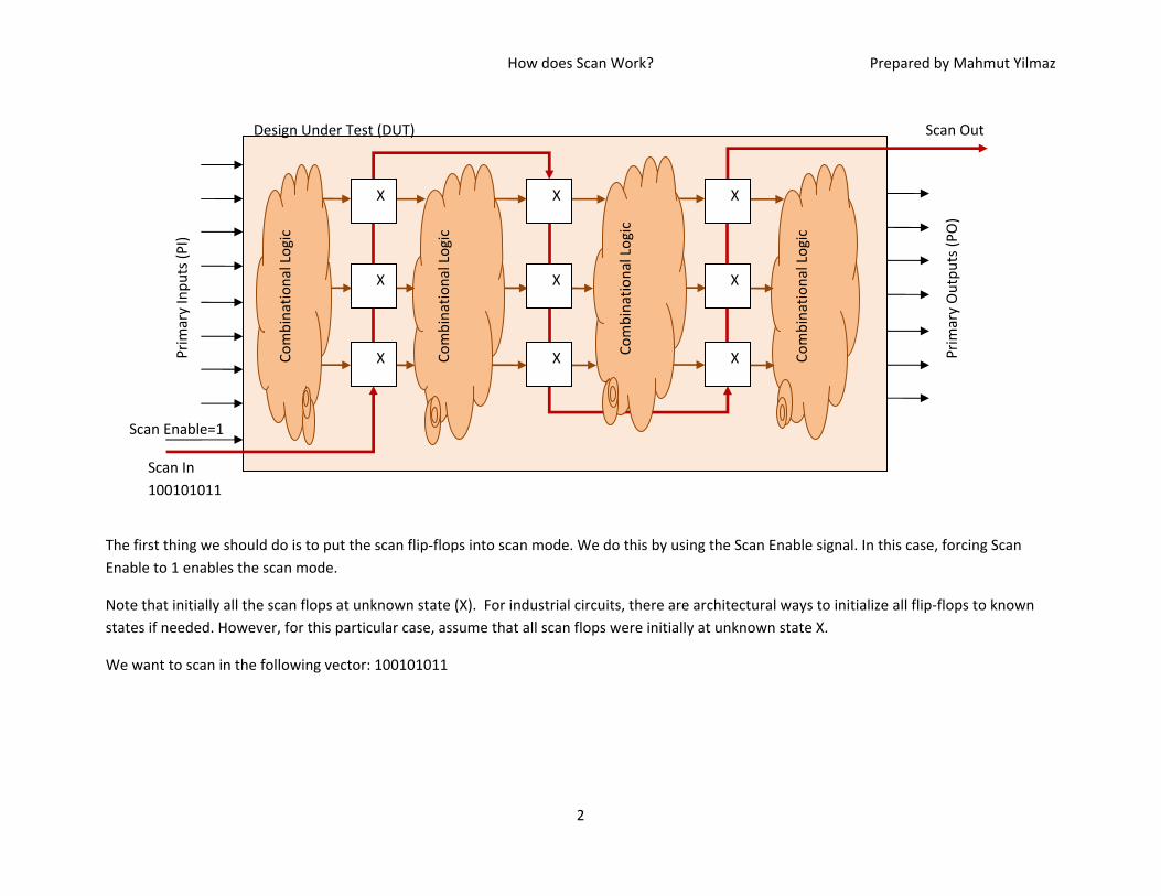
The first thing we should do is to put the scan flip‐flops into scan mode. We do this by using the Scan Enable signal. In this case, forcing Scan Enable to 1 enables the scan mode.
Note that initially all the scan flops at unknown state (X). For industrial circuits, there are architectural ways to initialize all flip‐flops to known states if needed. However, for this particular case, assume that all scan flops were initially at unknown state X.
We want to scan in the following vector: 100101011
2
How does Scan Work? Prepared by Mahmut Yilmaz
Design Under Test (DUT)
Combinatio
nal Logic
0
1
1
Combinatio
nal Logic
X
X
X
X
X
X Combinatio
nal Logic
Combinatio
nal Logic
Scan Enable=1
Prim
ary Outpu
ts (P
O)
Prim
ary Inpu
ts (P
I)
Scan Out
Scan In 100101
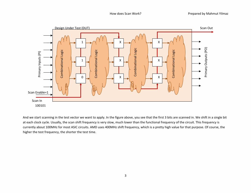
And we start scanning in the test vector we want to apply. In the figure above, you see that the first 3 bits are scanned in. We shift in a single bit at each clock cycle. Usually, the scan shift frequency is very slow, much lower than the functional frequency of the circuit. This frequency is currently about 100MHz for most ASIC circuits. AMD uses 400MHz shift frequency, which is a pretty high value for that purpose. Of course, the higher the test frequency, the shorter the test time.
3
How does Scan Work? Prepared by Mahmut Yilmaz
Design Under Test (DUT)
Combinatio
nal Logic
Prim
ary Inpu
ts (P
I)
Scan In
Prim
ary Outpu
ts (P
O)
1
0
0
Combinatio
nal Logic
0
1
1
1
0
1
Combinatio
nal Logic
Combinatio
nal Logic
Scan Enable=0
Scan Out
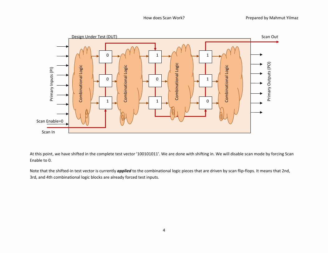
At this point, we have shifted in the complete test vector '100101011'. We are done with shifting in. We will disable scan mode by forcing Scan Enable to 0.
Note that the shifted‐in test vector is currently applied to the combinational logic pieces that are driven by scan flip‐flops. It means that 2nd, 3rd, and 4th combinational logic blocks are already forced test inputs.
4
How does Scan Work? Prepared by Mahmut Yilmaz
Design Under Test (DUT)
Combinatio
nal Logic
1
1
1
0
1
1
0
0
0
1
0
0
0
1
0
1
0
0
0
1
0
1
0
0
Combinatio
nal Logic
1
1
1
0
1
1
1
0
1
Combinatio
nal Logic
Combinatio
nal Logic
Scan Enable=0
Prim
ary Outpu
ts (P
O)
Prim
ary Inpu
ts (P
I)
Scan Out
Scan In
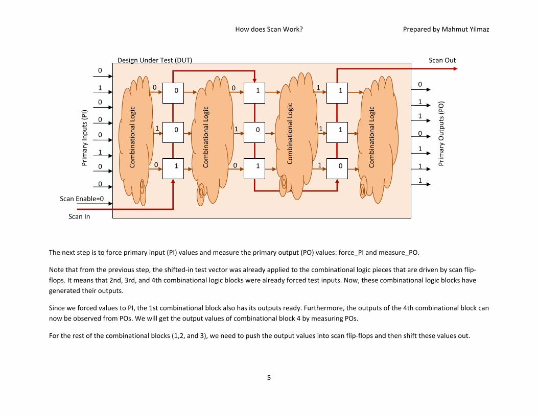
The next step is to force primary input (PI) values and measure the primary output (PO) values: force_PI and measure_PO.
Note that from the previous step, the shifted‐in test vector was already applied to the combinational logic pieces that are driven by scan flip‐flops. It means that 2nd, 3rd, and 4th combinational logic blocks were already forced test inputs. Now, these combinational logic blocks have generated their outputs.
Since we forced values to PI, the 1st combinational block also has its outputs ready. Furthermore, the outputs of the 4th combinational block can now be observed from POs. We will get the output values of combinational block 4 by measuring POs.
For the rest of the combinational blocks (1,2, and 3), we need to push the output values into scan flip‐flops and then shift these values out.
5
How does Scan Work? Prepared by Mahmut Yilmaz
Design Under Test (DUT)
Combinatio
nal Logic
1
1
1
0
1
0
1
0
0
1
0
0
0
1
0
Combinatio
nal Logic
Combinatio
nal Logic
0
1
0
0
1
0
1
1
1
0
1
0
0
1
0
1
1
1 Combinatio
nal Logic
Prim
ary Outpu
ts (P
O)
Prim
ary Inpu
ts (P
I)
Scan In
Scan Enable=0
Scan Out
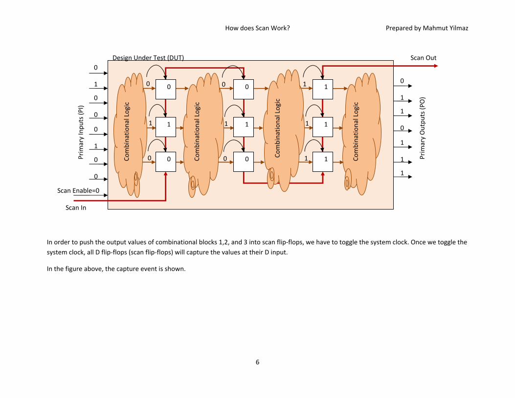
In order to push the output values of combinational blocks 1,2, and 3 into scan flip‐flops, we have to toggle the system clock. Once we toggle the system clock, all D flip‐flops (scan flip‐flops) will capture the values at their D input.
In the figure above, the capture event is shown.
6
How does Scan Work? Prepared by Mahmut Yilmaz
Design Under Test (DUT)
Combinatio
nal Logic
0
0
1
Combinatio
nal Logic
1
1
1
0
1
0
Combinatio
nal Logic
Combinatio
nal Logic
Prim
ary Outpu
ts (P
O)
Prim
ary Inpu
ts (P
I)
Scan In 111100111
Scan Enable=1
Scan Out
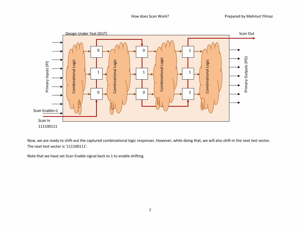
Now, we are ready to shift‐out the captured combinational logic responses. However, while doing that, we will also shift‐in the next test vector. The next test vector is '111100111'.
Note that we have set Scan Enable signal back to 1 to enable shifting.
7
How does Scan Work? Prepared by Mahmut Yilmaz
Design Under Test (DUT)
Combinatio
nal Logic
0
1
1
Combinatio
nal Logic
0
0
1 1
0
1 Combinatio
nal Logic
Combinatio
nal Logic
0111
Prim
ary Outpu
ts (P
O)
Prim
ary Inpu
ts (P
I)
Scan In 11110
Scan Enable=1
Scan Out
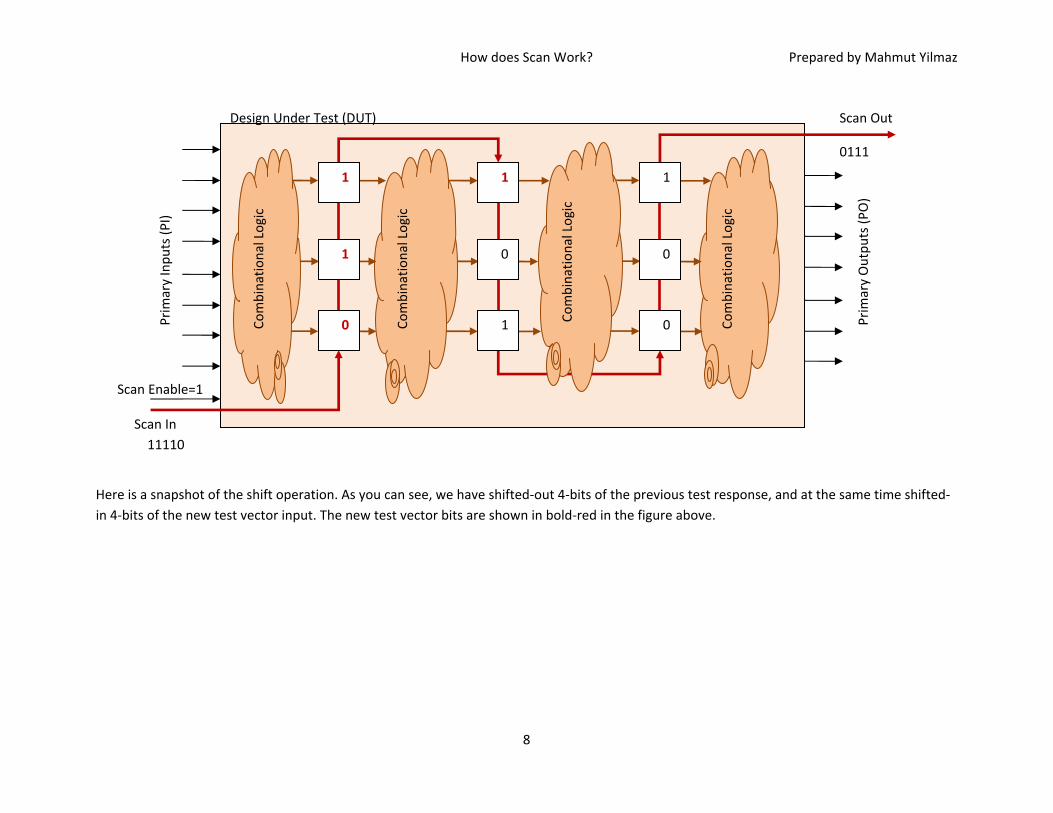
Here is a snapshot of the shift operation. As you can see, we have shifted‐out 4‐bits of the previous test response, and at the same time shifted‐in 4‐bits of the new test vector input. The new test vector bits are shown in bold‐red in the figure above.
8
How does Scan Work? Prepared by Mahmut Yilmaz
Design Under Test (DUT)
Combinatio
nal Logic
0
1
1
Combinatio
nal Logic
1
1
1 1
0
0 Combinatio
nal Logic
Combinatio
nal Logic
011000111
Prim
ary Outpu
ts (P
O)
Prim
ary Inpu
ts (P
I)
Scan In
Scan Enable=1
Scan Out
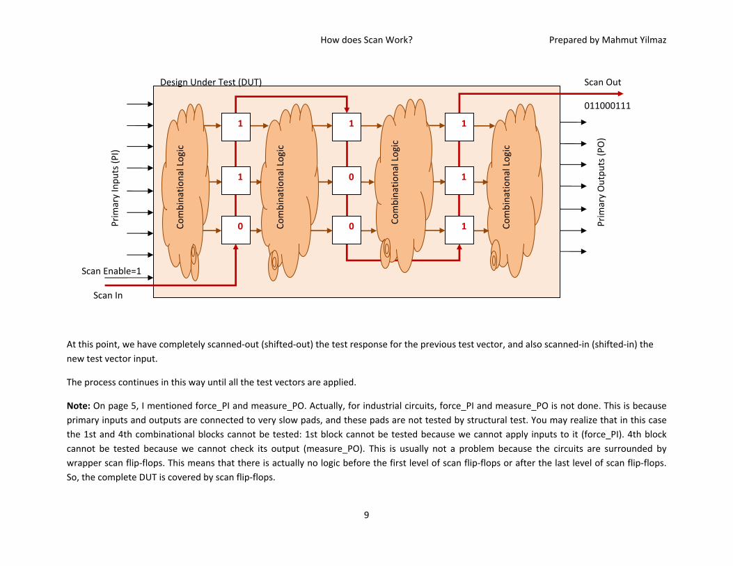
At this point, we have completely scanned‐out (shifted‐out) the test response for the previous test vector, and also scanned‐in (shifted‐in) the new test vector input.
The process continues in this way until all the test vectors are applied.
Note: On page 5, I mentioned force_PI and measure_PO. Actually, for industrial circuits, force_PI and measure_PO is not done. This is because primary inputs and outputs are connected to very slow pads, and these pads are not tested by structural test. You may realize that in this case the 1st and 4th combinational blocks cannot be tested: 1st block cannot be tested because we cannot apply inputs to it (force_PI). 4th block cannot be tested because we cannot check its output (measure_PO). This is usually not a problem because the circuits are surrounded by wrapper scan flip‐flops. This means that there is actually no logic before the first level of scan flip‐flops or after the last level of scan flip‐flops. So, the complete DUT is covered by scan flip‐flops.
9
How does Scan Work? Prepared by Mahmut Yilmaz
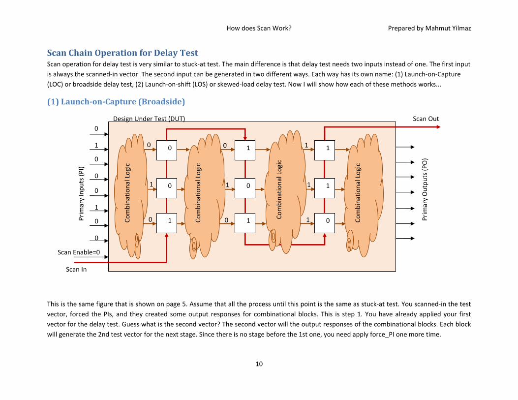
Scan Chain Operation for Delay Test Scan operation for delay test is very similar to stuck‐at test. The main difference is that delay test needs two inputs instead of one. The first input is always the scanned‐in vector. The second input can be generated in two different ways. Each way has its own name: (1) Launch‐on‐Capture (LOC) or broadside delay test, (2) Launch‐on‐shift (LOS) or skewed‐load delay test. Now I will show how each of these methods works...
(1) LaunchonCapture (Broadside)
Design Under Test (DUT)
Combinatio
nal Logic
0
0
1
0
0
0
1
0
0
0
1
0
1
0
1
0
0
Combinatio
nal Logic
1
1
1
0
1
1
1
0
1
Combinatio
nal Logic
Combinatio
nal Logic
Scan Enable=0
Prim
ary Outpu
ts (P
O)
Prim
ary Inpu
ts (P
I)
Scan Out
Scan In
This is the same figure that is shown on page 5. Assume that all the process until this point is the same as stuck‐at test. You scanned‐in the test vector, forced the PIs, and they created some output responses for combinational blocks. This is step 1. You have already applied your first vector for the delay test. Guess what is the second vector? The second vector will the output responses of the combinational blocks. Each block will generate the 2nd test vector for the next stage. Since there is no stage before the 1st one, you need apply force_PI one more time.
10
How does Scan Work? Prepared by Mahmut Yilmaz
Combinatio
nal Logic
0Prim
ary Inpu
ts (P
I)
Scan In
Prim
ary Outpu
ts (P
O)
1
1
1
0
1
1
0
1
0
0
0
1
0
0
1
1
1
0
1
1
0
1
0Combinatio
nal Logic
Combinatio
nal Logic
0
0
1 1
1
0
1
1
1
0
0
1
0
0
1
1
1 Co
mbinatio
nal Logic
Design Under Test (DUT)
Scan Enable=0
Scan Out
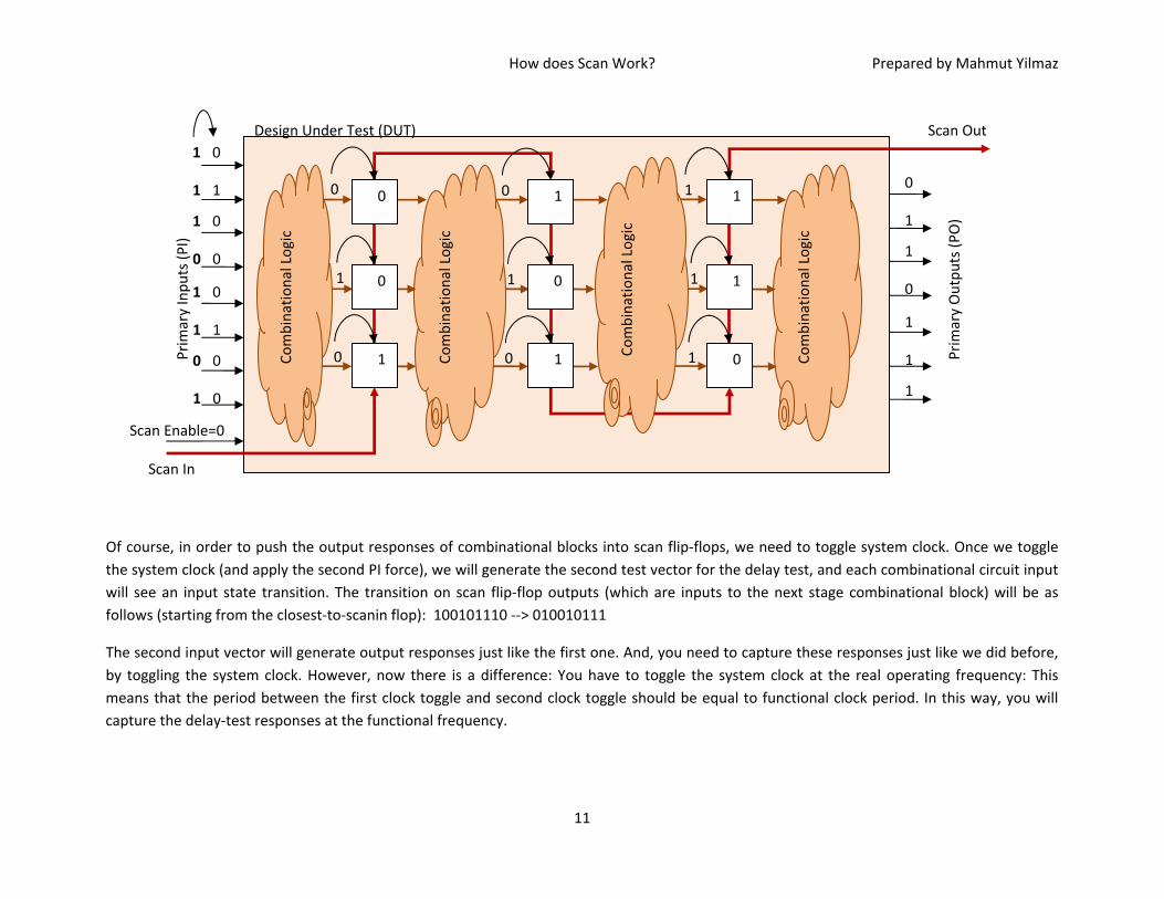
Of course, in order to push the output responses of combinational blocks into scan flip‐flops, we need to toggle system clock. Once we toggle the system clock (and apply the second PI force), we will generate the second test vector for the delay test, and each combinational circuit input will see an input state transition. The transition on scan flip‐flop outputs (which are inputs to the next stage combinational block) will be as follows (starting from the closest‐to‐scanin flop): 100101110 ‐‐> 010010111
The second input vector will generate output responses just like the first one. And, you need to capture these responses just like we did before, by toggling the system clock. However, now there is a difference: You have to toggle the system clock at the real operating frequency: This means that the period between the first clock toggle and second clock toggle should be equal to functional clock period. In this way, you will capture the delay‐test responses at the functional frequency.
11
How does Scan Work? Prepared by Mahmut Yilmaz
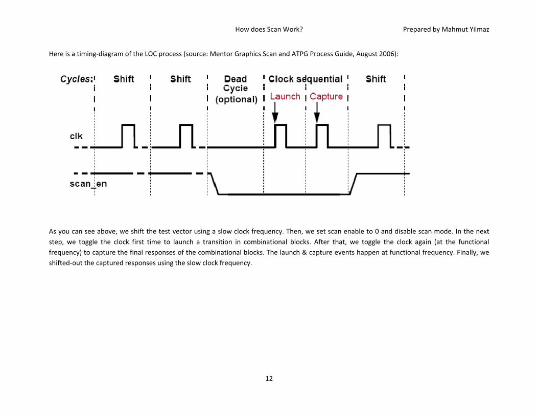
Here is a timing‐diagram of the LOC process (source: Mentor Graphics Scan and ATPG Process Guide, August 2006):
As you can see above, we shift the test vector using a slow clock frequency. Then, we set scan enable to 0 and disable scan mode. In the next step, we toggle the clock first time to launch a transition in combinational blocks. After that, we toggle the clock again (at the functional frequency) to capture the final responses of the combinational blocks. The launch & capture events happen at functional frequency. Finally, we shifted‐out the captured responses using the slow clock frequency.
12
How does Scan Work? Prepared by Mahmut Yilmaz
(2) LaunchonShift (SkewedLoad)
Design Under Test (DUT)
Combinatio
nal Logic
0
0
1
0
0
0
1
0
1
0
0
0
1
0
1
0
0
Combinatio
nal Logic
1
0
1
1
1
1
1
1
0 Combinatio
nal Logic
Combinatio
nal Logic
Scan Enable=1
Prim
ary Outpu
ts (P
O)
Prim
ary Inpu
ts (P
I)
Scan Out
Scan In
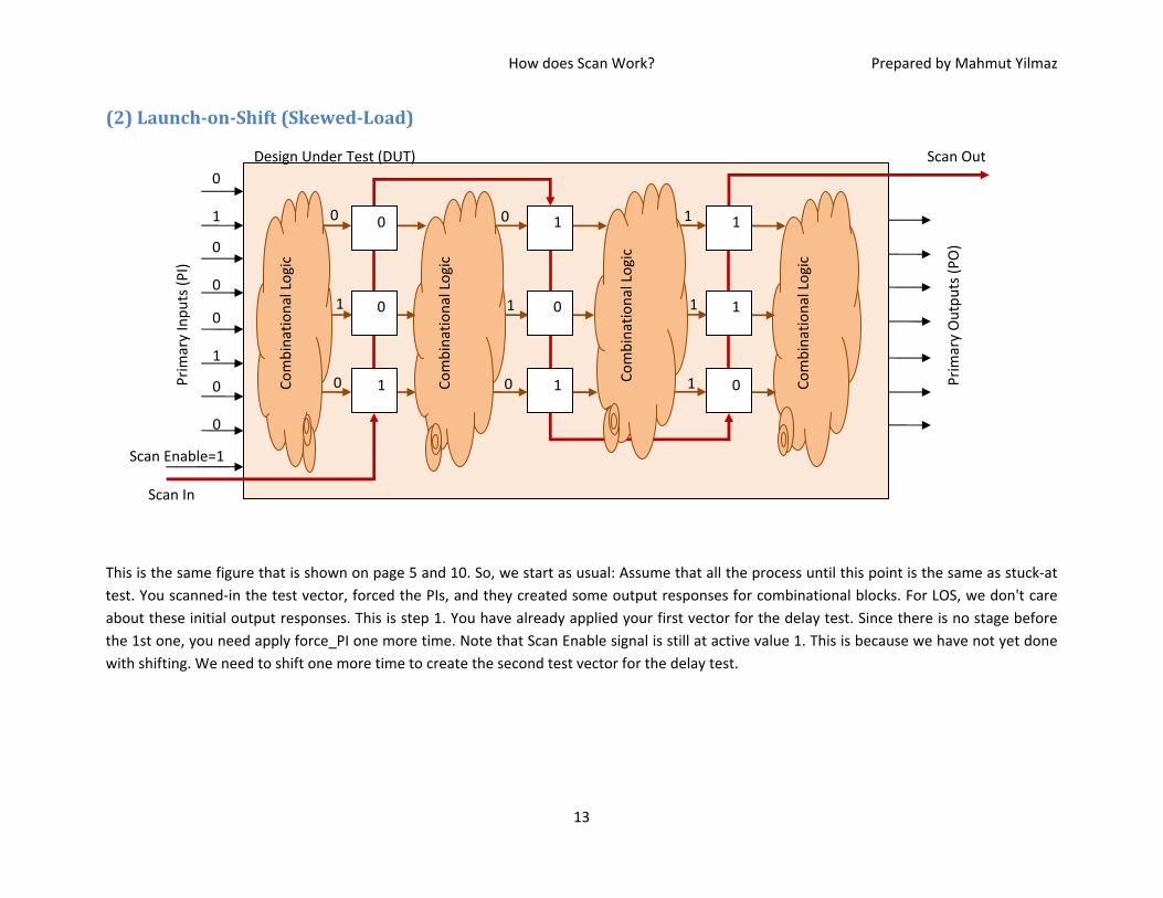
This is the same figure that is shown on page 5 and 10. So, we start as usual: Assume that all the process until this point is the same as stuck‐at test. You scanned‐in the test vector, forced the PIs, and they created some output responses for combinational blocks. For LOS, we don't care about these initial output responses. This is step 1. You have already applied your first vector for the delay test. Since there is no stage before the 1st one, you need apply force_PI one more time. Note that Scan Enable signal is still at active value 1. This is because we have not yet done with shifting. We need to shift one more time to create the second test vector for the delay test.
13
How does Scan Work? Prepared by Mahmut Yilmaz
Combinatio
nal Logic
Prim
ary Outpu
ts (P
O)
Prim
ary Inpu
ts (P
I)
Scan In
Scan Enable=1
Design Under Test (DUT)
Combinatio
nal Logic
Combinatio
nal Logic
Combinatio
nal Logic
0
0
1
1
0
1
1
1
0
0
1
0
0
0
1
0
0
1
1
1
0
1
1
0
1
0
1
0
0
1
0
1
1
1
0
Scan Out
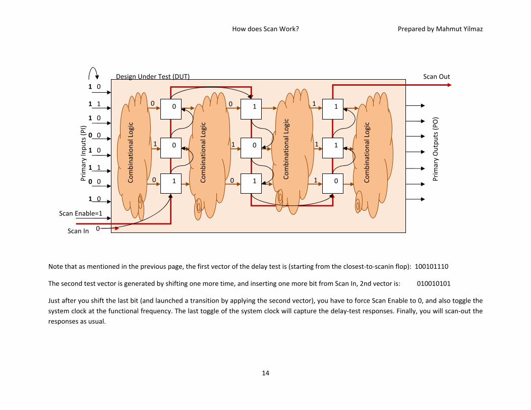
Note that as mentioned in the previous page, the first vector of the delay test is (starting from the closest‐to‐scanin flop): 100101110
The second test vector is generated by shifting one more time, and inserting one more bit from Scan In, 2nd vector is: 010010101
Just after you shift the last bit (and launched a transition by applying the second vector), you have to force Scan Enable to 0, and also toggle the system clock at the functional frequency. The last toggle of the system clock will capture the delay‐test responses. Finally, you will scan‐out the responses as usual.
14
How does Scan Work? Prepared by Mahmut Yilmaz
15
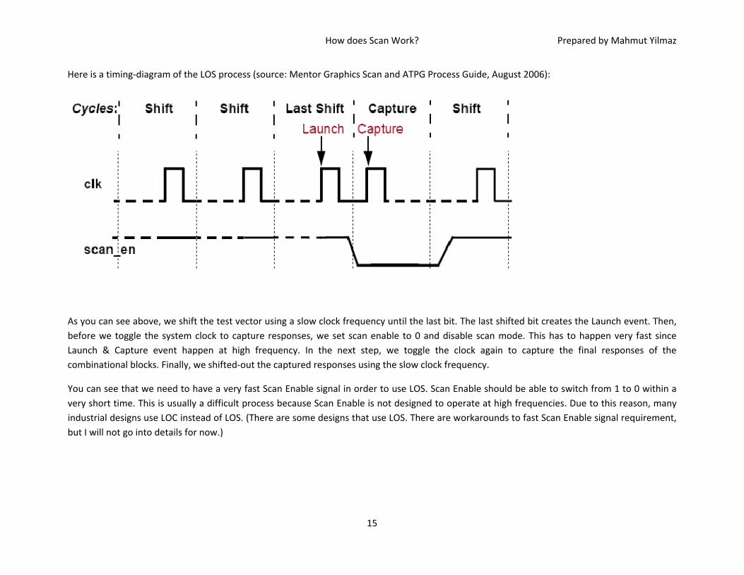
You can see that we need to have a very fast Scan Enable signal in order to use LOS. Scan Enable should be able to switch from 1 to 0 within a very short time. This is usually a difficult process because Scan Enable is not designed to operate at high frequencies. Due to this reason, many industrial designs use LOC instead of LOS. (There are some designs that use LOS. There are workarounds to fast Scan Enable signal requirement, but I will not go into details for now.)
As you can see above, we shift the test vector using a slow clock frequency until the last bit. The last shifted bit creates the Launch event. Then, before we toggle the system clock to capture responses, we set scan enable to 0 and disable scan mode. This has to happen very fast since Launch & Capture event happen at high frequency. In the next step, we toggle the clock again to capture the final responses of the combinational blocks. Finally, we shifted‐out the captured responses using the slow clock frequency.
Here is a timing‐diagram of the LOS process (source: Mentor Graphics Scan and ATPG Process Guide, August 2006):