digital caliper design utilizing an optical distance ...eet.etec.wwu.edu/sessioc/team/docs/digital...
TRANSCRIPT
_________________________________
Digital Caliper Design Utilizing an
Optical Distance Measuring Sensor
Calvin A. Sessions Christopher Wittmier
Jonathan Law Instrumentation Design Team Project
December 1, 2004
Western Washington University Electronics Engineering Technology
ETEC 377, Professor Grady
_________________________________

1
INTRODUCTION
Overall Objective
The overall objective of this instrumentation team project was to gain
research and design experience while further developing and enhancing
cooperative teamwork skills. In the span of two months, this project allowed our
members to step through the actual design process from conception and design,
to prototype development.
Project Purpose
In particular, our instrumentation design team developed a digital caliper
utilizing an optical distance measuring sensor. This method was chosen as a
unique and interesting technique to process information measured by a caliper.
The function of the digital caliper was designed to be able to optically measure
the dimensions of small objects, electronically eliminating human error
generated from analog/mechanical calipers or other measuring tools. It was
decided that the design had to be portable, inexpensive, and perform with
accurate precision. Its use would be best suited for a laboratory environment;
therefore it was appropriate that our design utilized standard SI units: 0mm –
99.9mm range.

FUNCTIONAL DESCRIPTION
As shown in the system block diagram in Figure 1, there were four main
procedures conceptualized in the digital caliper design. First, a physical process
had to be changed into some type of electronic signal. In this project a
transducer was implemented to convert the physical process into a voltage.
Then the analog signal obtained from the transducer output had to be
conditioned and scaled through signal processing circuitry. The processed
analog signal was then digitized with an A/D converter, and finally displayed.
Figure 1: Digital Caliper System Block Diagram
The Sharp GP2D12 distance measuring sensor was implemented as the
transducer in the electronic design. Characteristics of this particular sensor will
be discussed in great detail later in this document. Because the output produced
from the GP2D12 is an analog, nonlinear voltage, the last three stages of the
system block diagram shown in Figure 1 required the most attention.
2
3
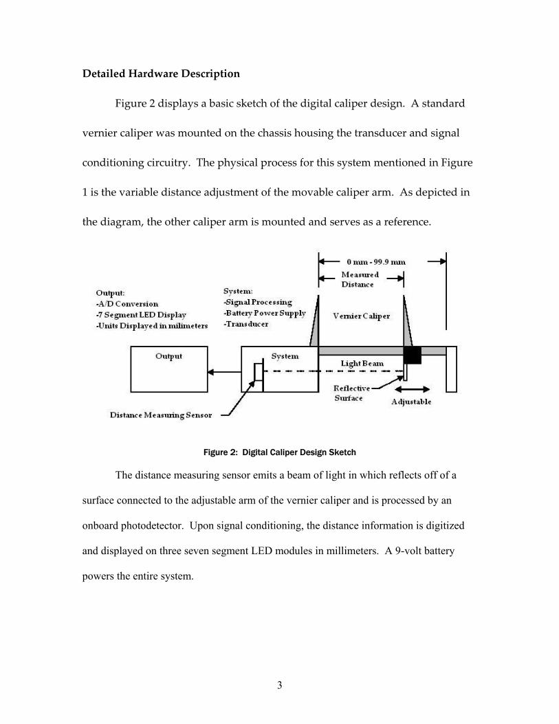
Detailed Hardware Description
Figure 2 displays a basic sketch of the digital caliper design. A standard
vernier caliper was mounted on the chassis housing the transducer and signal
conditioning circuitry. The physical process for this system mentioned in Figure
1 is the variable distance adjustment of the movable caliper arm. As depicted in
the diagram, the other caliper arm is mounted and serves as a reference.
Figure 2: Digital Caliper Design Sketch
The distance measuring sensor emits a beam of light in which reflects off of a
surface connected to the adjustable arm of the vernier caliper and is processed by an
onboard photodetector. Upon signal conditioning, the distance information is digitized
and displayed on three seven segment LED modules in millimeters. A 9-volt battery
powers the entire system.

4
Distance Measuring Sensor
Figure 3 displays images and dimensions of the Sharp GP2D12 distance
measuring sensor. This device contains both an infrared light source and a
photodetector.
Figure 3: Sharp GP2D12 Images Figure 4: GP2D12 Measuring Function
According to the Robotic Society of Southern California (RSSC) website,
light is emitted from the infrared LED through a lens which focuses the beam on
a small spot of the measured object. The light then reflects off of the object to the
position sensitive device (PSD), as shown in Figure 4. This is referred to as the
optical triangulation principal. Also stated on the RSSC website, as the distance
to the sensed object changes, the spot of light moves on the position-sensitive
detector, and a different distance is reported.
5
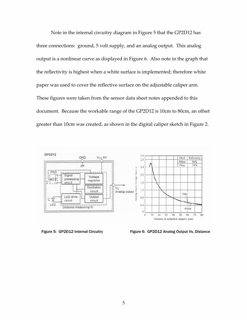
Note in the internal circuitry diagram in Figure 5 that the GP2D12 has
three connections: ground, 5 volt supply, and an analog output. This analog
output is a nonlinear curve as displayed in Figure 6. Also note in the graph that
the reflectivity is highest when a white surface is implemented; therefore white
paper was used to cover the reflective surface on the adjustable caliper arm.
These figures were taken from the sensor data sheet notes appended to this
document. Because the workable range of the GP2D12 is 10cm to 80cm, an offset
greater than 10cm was created, as shown in the digital caliper sketch in Figure 2.
Figure 5: GP2D12 Internal Circuitry Figure 6: GP2D12 Analog Output Vs. Distance

6
Signal Processing
The output of the analog distance measuring sensor signal resembles a
decaying logarithmic function. To correct this nonlinear characteristic, a
logarithmic amplifier was constructed a stage after the transducer. This was
performed by placing a diode in the feedback of an operational amplifier.
Though the output signal was more linear, a decaying output with respect
to the increasing distance was present. Therefore a summing amplifier was
constructed. This summing amplifier consisted of amplifying the negative
linearized output and adding it to an offset voltage. The output of the summing
amplifier was designed to yield a range from 0 volts for 0mm to .100 volts for
100mm.
Because the output of the summing amplifier yielded a negative voltage,
an inverting amplifier with a gain of 10 was implemented. This gain was
necessary because the A/D converter and output circuitry required a 0 to 1.0 volt
working range. Figure 7 depicts a general block diagram of the signal
conditioning procedures.
Figure 7: Signal Processing Block Diagram

7
A/D Conversion and Output Display
Range: 0mm-99.9mm Units: milimters
Figure 8: 7 Segment LED Module Display
Having previously linearized and scaled the input voltage, the function of
the A/D section was essentially that of a voltmeter. Intersil’s CA3162E dual slope
A/D converter was chosen for its appropriate range and precision, featuring
three onboard multiplexing lines designed specifically for use in three-digit
displays. These lines were used to enable three 7-segment LED modules, as
pictured above, driven sequentially by a single 74LS247 BCD - Seven segment
display driver. PNP transistors were used as multiplexing switches, and the
74LS247’s open collector outputs were pulled up with a resistor network. The
converter operates at 4Hz, using the built in timing of the CA3162E in low speed-
mode. Although the display’s tenth of a millimeter resolution is somewhat
useless given the overall caliper error of over one millimeter, this provides for
later improvement of transducer linearization, were more time allotted.
8
PROTOTYPE DEVELOPMENT
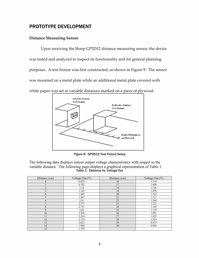
Distance Measuring Sensor
Upon receiving the Sharp GP2D12 distance measuring sensor, the device
was tested and analyzed to inspect its functionality and for general planning
purposes. A test fixture was first constructed, as shown in Figure 9. The sensor
was mounted on a metal plate while an additional metal plate covered with
white paper was set at variable distances marked on a piece of plywood.
Figure 9: GP2D12 Test Fixture Setup
The following data displays sensor output voltage characteristics with respect to the variable distance. The following page displays a graphical representation of Table 1.
Table 1: Distance Vs. Voltage Out
Distance (cm) Voltage Out (V) Distance (cm) Voltage Out (V) 0 0.029 16 1.710 1 0.702 17 1.609 2 1.18 18 1.526 3 1.145 19 1.470 4 1.805 20 1.392 5 1.847 21 1.317 6 2.01 22 1.268 7 2.577 23 1.223 8 2.751 24 1.166 9 2.66 25 1.129
10 2.508 26 1.091 11 2.334 27 1.052 12 2.176 28 1.014 13 2.033 29 0.975 14 1.904 30 0.956 15 1.795

9
Graph 1: Distance Vs. Voltage Out
0 2 4 6 8 10 12 14 16 18 20 22 24 26 28 300
0.5
1
1.5
2
2.5
3Distance vs. Voltage Out
Distance (cm)
Vol
tage
Out
(V)
Vo
distance
Signal Processing and Power Supply:
The following table displays the sensor output using a logarithmic
amplifer with respect to a varying distance:
Table 2: Distance Vs. Voltage Out – w/ log amp
Distance Voltage Out Distance Voltage Out 8 0.653 20 0.626 9 0.653 21 0.625
10 0.651 22 0.623 11 0.648 23 0.621 12 0.645 24 0.619 13 0.643 25 0.617 14 0.638 26 0.615 15 0.636 27 0.614 16 0.635 28 0.612 17 0.633 29 0.611 18 0.631 30 0.610 19 0.629
10
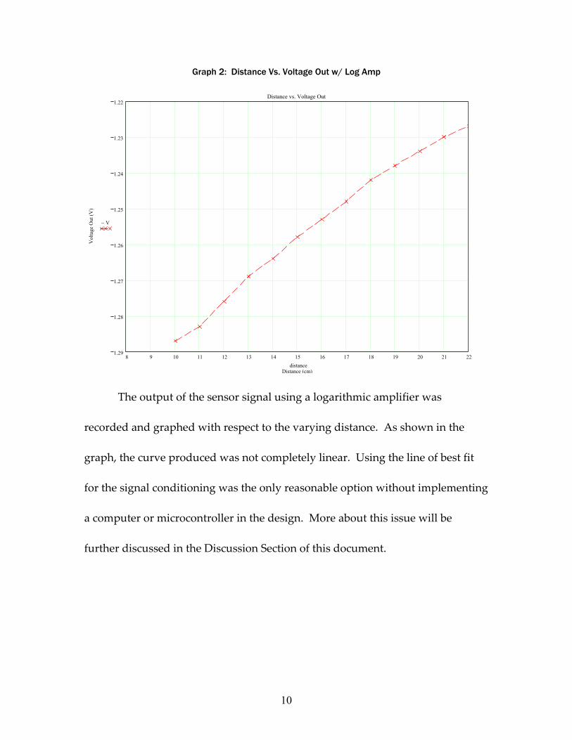
Graph 2: Distance Vs. Voltage Out w/ Log Amp
8 9 10 11 12 13 14 15 16 17 18 19 20 21 221.29
1.28
1.27
1.26
1.25
1.24
1.23
1.22Distance vs. Voltage Out
Distance (cm)
Vol
tage
Out
(V)
V−
distance
The output of the sensor signal using a logarithmic amplifier was
recorded and graphed with respect to the varying distance. As shown in the
graph, the curve produced was not completely linear. Using the line of best fit
for the signal conditioning was the only reasonable option without implementing
a computer or microcontroller in the design. More about this issue will be
further discussed in the Discussion Section of this document.

11
+3
-2
V+
4V
-11
OUT 1
U1A
TL084
+5
-6
V+4
V-
11
OUT7
U1B
TL084
+10
-9
V+
4V-
11
OUT8
U1C
TL084
D1D1N4148
00
0
0
IN1
OUT2
GN
D3
U2
Sharp GP2D12
R1
1k R2
4.99k
R3
20k
R4
20k
R51.02k
R61k
R7
2k
R8
20kR9
150
R10150
C110u
-5V
-5V
-5V
+5V
+5V
+5V
+5V
+5V
0
C210u
0
Signal Conditioning
IN1
OUT2
GN
D3
U4 GL7805
-+
+-
U5
TC7662A
C610u
C710u
0
C810u
0
0
V29Vdc
0
-5V
+5V
Charge Pump
Voltage RegulatorPower Supply
The following schematic diagram and signal conditioning equations were
implemented, shown in Figure 2. This circuit was described in the Detailed
Hardware Description. The transducer, signal processing circuitry, and power
supply circuitry was soldered onto a single protoboard. The power supply circuitry
is also displayed below.
Schematic 1: Signal Conditioning Schematic
Summing Amplifier/Signal Conditioning Calculations Distance (cm) Sensor Output w/ Log Amp (volts)
0 cm - 0.626 volts 10 cm - 0.600 volts
Equation 1: 0 = - 0.626 m + Voffset Equation 2: 0.1 = -0.600 m + Voffset m = 3.84615 GAIN Voffset = 2.40769 volts
Schematic 2: Power Supply Schematic

12
Image 1: Power Supply and Signal Processing Circuitry
Image 2: Power Supply and Signal Processing Assembly

13
A/D Conversion and Output Display
Illustrated in the schematic below, the complexity of the A/D converter and
display design was greatly reduced by the CA3162E’s built-in features. Initially, an
AD0804 converter was considered which would have provided an 8-bit binary output.
This converter was dropped, as 3 cascaded ‘185 decoders (or a PLD) would have been
required to produce a displayable decimal output. In determining conversion speed, the
CA3162E offered two built in speed modes. High speed mode (96Hz) would have
produced unreadable display flicker, leaving 4Hz low-speed mode. Ideally, an even
lower speed would be used, as there is still some degree of annoying flicker. To achieve
this, a sample-holding pulse circuit was designed and constructed using a 555 timer.
Although this pulse provided the variable sampling intended, the timing could not be
adjusted much below 4Hz before appearing very sluggish. Thus, the circuit was excluded
in the final prototype as the minor benefits provided did not seem to justify the additional
hardware.
Schematic 3: ADC and Digital Output Schematic
14
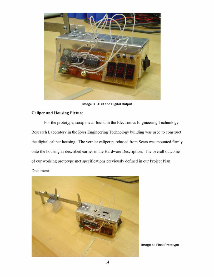
Image 3: ADC and Digital Output
Caliper and Housing Fixture
For the prototype, scrap metal found in the Electronics Engineering Technology
Research Laboratory in the Ross Engineering Technology building was used to construct
the digital caliper housing. The vernier caliper purchased from Sears was mounted firmly
onto the housing as described earlier in the Hardware Description. The overall outcome
of our working prototype met specifications previously defined in our Project Plan
Document.
Image 4: Final Prototype

15
Image 5: Final Prototype
DISCUSSION
Given the small amount of time to design, test, and construct the final
instrumentation prototype, we as a group are satisfied with the outcome our project.
However, there are a significant amount of aspects in the design project that can be
improved or even performed differently.
The final prototype display flickers between a few millimeters due to noise issues.
From our observations, the GP2D12 generates a noisy analog signal, therefore a 10uF
capacitor was placed in between the output signal and ground. The noise that does not
get filtered becomes amplified after the various stages of operational amplifiers. Two
other 10uF capacitors were utilized to filter the final analog output signal in the signal
conditioning stage and in between the 5 volt and ground buses. It was also observed that
more noise is introduced as the 9 volt battery drains. From this, we noted that our design
consumes a lot of power.

16
A large issue that determines the accuracy of the digital caliper is the linearization
technique used to condition the sensor signal. As shown in the Prototype Development
Section of this document, the output signal of the sensor after 10 cm is not exactly
logarithmic. It was later discovered in the GP2D12 Application Notes that the output is
more like a 1/X function. We attempted to create a dividing amplifier utilizing two
logarithmic amplifiers, a difference amplifier, followed by an antilog amplifier, however
this process failed. Perhaps if this issue came to our attention sooner, a dividing
amplifier IC could have been ordered.
Another technique that could have corrected the linearization problem was
implementing a microcontroller or computer. A look-up table would be created to match
the correct distance output with the sensor signal. This idea was first discussed during
the project conceptualization phase, but it prevented our team from learning about the
various stages involved in analog signal processing and digitizing the output.
This was our first attempt to design and build a working electronic
instrumentation project on a design team. Further developing our teamwork skills in a
cooperative environment has better prepared us for industry.
17
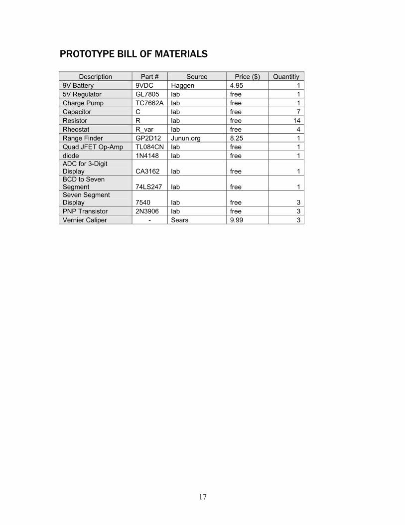
PROTOTYPE BILL OF MATERIALS
Description Part # Source Price ($) Quantitiy 9V Battery 9VDC Haggen 4.95 1 5V Regulator GL7805 lab free 1 Charge Pump TC7662A lab free 1 Capacitor C lab free 7 Resistor R lab free 14 Rheostat R_var lab free 4 Range Finder GP2D12 Junun.org 8.25 1 Quad JFET Op-Amp TL084CN lab free 1 diode 1N4148 lab free 1 ADC for 3-Digit Display CA3162 lab free 1 BCD to Seven Segment 74LS247 lab free 1 Seven Segment Display 7540 lab free 3 PNP Transistor 2N3906 lab free 3 Vernier Caliper - Sears 9.99 3