digital microfluidic biochips: recent research and ...paupo/publications/ho2011aa-digital...
TRANSCRIPT

Digital Microfluidic Biochips:Recent Research and Emerging Challenges
Tsung-Yi HoDept. of Computer Scienceand Information EngineeringNational Cheng Kung Univ.
Tainan, [email protected]
Krishnendu ChakrabartyDepartment of Electrical and
Computer EngineeringDuke University
Durham, NC, [email protected]
Paul PopDTU Informatics
Technical University ofDenmark
Kgs. Lyngby, [email protected]
ABSTRACTMicrofluidic biochips are replacing the conventional biochemicalanalyzers, and are able to integrate on-chip all the basic functionsfor biochemical analysis. The “digital” microfluidic biochips (DM-FBs) are manipulating liquids not as a continuous flow, but as dis-crete droplets on a two-dimensional array of electrodes. Basic mi-crofluidic operations, such as mixing and dilution, are performedon the array, by routing the corresponding droplets on a series ofelectrodes. The challenges facing biochips are similar to thosefaced by microelectronics some decades ago. To meet the chal-lenges of increasing design complexity, computer-aided-design (C-AD) tools are being developed for DMFBs. This paper providesan overview of DMFBs and describes emerging CAD tools forthe automated synthesis and optimization of DMFB designs, fromfluidic-level synthesis and chip-level design to testing. Design au-tomations are expected to alleviate the burden of manual optimiza-tion of bioassays, time-consuming chip designs, and costly testingand maintenance procedures. With the assistance of CAD tools,users can concentrate on the development and abstraction of nanos-cale bioassays while leaving chip optimization and implementationdetails to CAD tools.Categories and Subject Descriptors: B.7.2 [Integrated Circuits]:Design Aids; B.8.2 [Performance and Reliability]: PerformanceAnalysis and Design Aids; J.3 [Life and Medical Sciences]: Biol-ogy and genetics, HealthGeneral Terms: Algorithms, Performance, Design, ReliabilityKeywords: Microfluidics, biochips, design automation
1. INTRODUCTIONMicrofluidic-based biochips are soon revolutionizing clinical di-
agnostics and many biochemical laboratory procedures due to theiradvantages of automation, cost reduction, portability, and efficiency[32]. Conventional technology depends on the manipulation ofcontinuous liquid flow through microfabricated channels. How-ever, actuation of flow is implemented with external assistance ofmicro-pump and micro-valve, which are complex and cumbersome.
Permission to make digital or hard copies of all or part of this work forpersonal or classroom use is granted without fee provided that copies arenot made or distributed for profit or commercial advantage and that copiesbear this notice and the full citation on the first page. To copy otherwise, torepublish, to post on servers or to redistribute to lists, requires prior specificpermission and/or a fee.CODES+ISSS’11, October 9–14, 2011, Taipei, Taiwan.Copyright 2011 ACM 978-1-4503-0715-4/11/10 ...$10.00.
Moreover, permanently-etched channels greatly restrict the feasi-bility and versatility. Therefore, microfluidic research is witness-ing a paradigm shift from the continuous-flow-based architectureto droplet-based architecture or, in particular, the digital microflu-idic biochip (DMFB) [6, 12, 19, 32].
Detector
ActuatedDroplets
Electrodes(2D array)
Mixingoperation
Dispensingport
Figure 1: The schematic view of a DMFB.
Generally, a DMFB consists of a two-dimensional (2D) electrodearray and peripheral devices such as optical detector and dispens-ing port, as schematically shown in Figure 1 [12, 32]. The samplecarriers, droplets, being miniaturized and discretized liquids, arecontrolled by underlying electrodes using electrical actuations (i.e.,a principle called electrowetting-on-dielectric or EWOD) [25]. Byassigning time-varying voltage values to turn on/off electrodes, dro-plets can be moved around the entire 2D array to perform funda-mental operations (e.g., dispensing and mixing) [28]. These opera-tions are carried out in a reconfigurable manner due to their flexibil-ity in area and time domain [6]. Compared with continuous-flow-based biochips, DMFBs offer various advantages including moreflexible control mechanism and higher throughput and sensitivityas well as lower sample/reagent volume consumption.
Due to these advantages, DMFBs have attracted many efforts be-ing devoted to marketplace demands, ranging from healthcare, en-vironmental sensing, and point-of-care-testing applications. As re-ported in Figure 2, the global market value for biochip products wasestimated to be $2.6 billion in 2009, but it is expected to increaseto nearly $6 billion in 2014, for a 5-year high compound-annual-growth-rate (CAGR) of 17.7% [2]. Continuing growth of variousapplications have dramatically complicated chip/system integrationand design complexity [7, 12], rendering traditional manual designsinfeasible, especially under time-to-market constraints. Hence, itis necessary to develop high-quality computer-aided-design (CAD)tools for efficient design automation. Design automations are ex-pected to reduce the burden associated with manual optimizationof bioassays, time-consuming chip designs, and costly testing andmaintenance procedures. Moreover, the assistance of CAD toolswill facilitate the integration of fluidic components with a micro-electronic component in next-generation system-on-chips (SOCs)[6, 7, 12, 32].
335

0500
10001500200025003000
2007 2008 2009 2014
DNA mircoarrayLab-on-a-chipProtein microarrayEmerging microarray
$M
illio
ns
Year
Global Value of Biochip Product
Figure 2: Global-value estimate of biochip products.
In this paper, we provide a survey of recent research and emerg-ing challenges in design and optimization for DMFBs. We showhow CAD approaches can be used to automate and optimize thedesign of DMFBs in fluidic domain and chip (i.e., hardware) do-main. The goal in this paper is to give a holistic perspective ontop-down system-level CAD tools, and discuss several associatedcombinatorial and geometric optimization problems. Having theseCAD tools, users and designers will be able to describe bioassays ata high-level of abstraction. CAD tools will generate an optimizedschedule of bioassay operations, a suitable chip layout for best flu-idic performance, and well-planed signal connections for low-costmanufacturing process. Therefore, biochip users and designers canconcentrate on innovations at the application level, leaving imple-mentation details to CAD tools. These CAD tools will reduce hu-man effort and enable high-volume production. The remainder ofthe paper is organized as follows: Section 2 reviews the typicalCAD flow of DMFB that consists of fluidic-level synthesis andchip-level design. Section 3 and section 4 discuss the related opti-mization problems and CAD approaches in fluidic-level synthesisand chip-level design, respectively. Section 5 examines defects,fault models, and testing techniques.
Section 6 describes the design challenges and several open prob-lems that remain to be tackled in the future. Finally, conclusion isdrawn in Section 7.
2. CAD FLOW OF DMFBSA regular CAD flow of DMFBs consists of two stages, fluidic-
level synthesis and chip-level design [12], as illustrated in Figure3. Fluidic-level synthesis describes an automated scheduling ofassays and a generation of a mapping of assay operations to re-sources in a time-multiplexed manner. Fluidic-level synthesis is di-vided into two major phases, referred to as architectural-level syn-thesis (i.e., high-level synthesis) and geometry-level synthesis (i.e.,physical design) [29, 30, 32]. Optimizations here are guaranteeinghigh-performance fluidic behaviors as well as a suitable chip lay-out. On the other hand, the goal in chip-level design is determiningthe control-signal plan and electrical connections for the electrodesto execute the synthesized result. Chip-level design consists of twosteps of electrode addressing followed by wire routing [12, 16].This design stage is receiving increasing attention in recent yearsas it dominates the manufacturing complexity and fabrication costof a DMFB.
In the following sections, we provide a progression of the relatedCAD problems and research on fluidic-level synthesis and chip-level design, respectively.
3. FLUIDIC-LEVEL SYNTHESISIn this section, we discuss automated fluidic-level synthesis.Hierarchical and cell-based design techniques from modern very-
(d) Used electrodes
1 2 24 3
5 6 79 8
34
10671112
13 14 15
O1 O2 O3
O5
O4
O1 O2O3
O4
O5
0
1
2
3
4
Timestep Mixer 1 Mixer 2 Mixer 3
Mixer 1 Mixer 2
Mixer 3
Droplet routing
Droplet(a) Sequencing graph (b) Scheduled result (c) Placement & Routing
Fluidic-level synthesisChip-level design
(e) Electrode addressing (f) Wiring solution
Pinassignment
Escape toI/O pads
Time-stepassignment
Chiplayout
Devicebinding
Controlpins
Conductionwires
Dropletbehaviors
Figure 3: Regular CAD flow of DMFBs consists of two stagesof fluidic-level synthesis followed by chip-level design.
large-scale-integration (VLSI) automation has been utilized for arc-hitectural-level synthesis and geometry-level synthesis.
3.1 Architectural-Level SynthesisAn assay is typically abstracted as a model of sequencing graph
(see Figure 3(a)). The sequencing graph is directed, acyclic andpolar (i.e., there is a source node without predecessors and a sinknode without successors). Each node represents a specific assayoperation (e.g., mixing, generation, and detection), while a directededge indicates the dependency between two operations.
In architectural-level synthesis, both the resource-binding prob-lem and the scheduling problem are addressed to generate a struc-tural view of a biochip design. As analogous to high-level synthe-sis for integrated circuits, resource binding determines a mappingfrom assay operations to available functional resources. There maybe several types of resources for any given assay operation. Forexample, a 2 ! 2 mixer and a 2 ! 3 mixer can be used for a mix-ing operation but with different mixing times. A resource bindingprocedure is applied to determine the selections with a minimizedassay execution time. Once resource binding is carried out, the exe-cution time for each assay operation can be roughly determined. Inother words, scheduling of the start times and stop times of all as-say operations is determined, subject to the precedence constraintsby the given sequencing graph, as illustrated in Figure 3(b).
Figure 4: Checkpoint insertion and re-execution subroutine[47].
Several algorithms, such as tabu-search based synthesis [23] andILP (integer-linear-programming) based synthesis [29], are pro-posed to handle the basic architectural-level synthesis of DMFBs.In addition, for some complex biomedical applications such as clin-ical diagnostics, it is necessary to verify the correctness of on-chip
336
fluidic operations. The status of an assay can be monitored by ex-amining the volume of the droplet, sample concentration, or detec-tor readout. If an error occurs during the execution of an assay, e.g.,an unexpected volume of an intermediate droplet, the assay out-comes will be misleaded. Therefore, it is important to detect sucherrors as early as possible and re-execute the fluidic operations toobtain correct assay outcomes. Considering this issue, a control-path based design is recently integrated to the architectural-levelsynthesis of DMFBs [47]. In [47], they first calculate the possibili-ties of errors for each operation via an error-propagation estimates,and then insert a check point consisting of a storing operation anda error detection to the sequencing graph, as shown in Figure 4. Asimulated-annealing (SA) method is also proposed to optimize theexecution time used for error recovery.
3.2 Geometry-Level SynthesisA key problem in the geometry-level (i.e., physical-level) syn-
thesis of DMFBs is the placement of fluidic modules such as dif-ferent types of mixers and detection units. The major goal of theplacement is to find the actual locations of different fluidic mod-ules corresponding to different time intervals. Since DMFBs enabledynamic reconfiguration of the microfluidic array during run-time,they allow the placement of different modules on the same locationduring different time intervals [31, 33]. Therefore, the placementof modules can be modeled as a three-dimensional (3D) packingproblem. Each fluidic module represents a 3D box, the base ofwhich denotes the rectangular area of the module and the heightdenotes the time span of its execution, see Figure 5 for an example.
Figure 5: 3D packing diagram of a placement result.
The most important optimization objective of the placement prob-lem is the minimization of chip area. Since solutions of the place-ment problem can provide the designers with guidelines on the chipsize to be manufactured, area minimization frees up more unit cellsfor other fluidic functions such as sample preparation and collec-tion. During the placement, some performance constraints includ-ing the upper limit on assay completion time and maximum allow-able chip array should be satisfied, in order that the system reli-ability and integrity inherent from the architectural-level synthesiscan be well-maintained. Besides, since the increasing assay densityand area of DMFBs may potentially reduce yield, a critical issue offault tolerance is also considered to avoid defective cells due tofabrication. Since we need time to ramp up the yield of DMFBs, itis desirable to perform a bioassay on a DMFB with the existence ofdefects (i.e., fabrication faults). How to integrate the defect tolerantissue into the placement problem with correct fluidic functions hasbecome an important issue. To handle such a problem, some al-gorithms, such as SA-based optimization [30, 33] and T-tree-basedplacement formulation [44], are presented in recent years. Besides,
a work in [4] further considers the control-path based synthesis withplacement to minimize the operation variability.
Droplet routing on DMFBs is a key design issue in the physical-level synthesis, which schedules the movement of each droplet in atime-multiplexed manner. The major goal of droplet routing is con-structing the connections between modules, and between modulesand I/O ports (i.e., on-chip reservoirs) within different time inter-vals. This physical synthesis is one of the most critical design chal-lenges due to design complexity as well as large impacts on cor-rect assay performance. Since a microfluidic array is reconfigureddynamically at run-time, the inherent reconfigurability allows dif-ferent droplet routes to share cells on the micorfluidic array duringdifferent time intervals. Besides, a series of 2D placement config-urations of fluidic modules in different time intervals are obtainedin the placement stage. Therefore, droplet routing is decomposedinto a series of sub-problems, which establishes the connectionsfor pre-placed fluidic modules between successive sub-problems.We can thus obtain a complete droplet routing solution by solvingthese sub-problems sequentially. In this sense, the routes on themicrofluidic array can be viewed as virtual routes in a 3D manner,which make the droplet routing problem different from the classi-cal wire routing in VLSI designs [34]. Systematic droplet routingmethods have therefore been developed to minimize the number ofcells used for droplet routing for better fault, while satisfying con-straints imposed by performance goals and fluidic properties [13,15, 34, 45, 49].
DsB24
S4
(a) (b)
Dlt23
Dlt24
Dlt20
DsB30
Dlt29
S1
S2
S3
DsB28
S3,5D3
D4
D5
D1
S2,3
S3,4
S4,5D2
S2,3
S3,4
S3,5
S4,5
W4,5
WR
WS
WS
WR
(c)
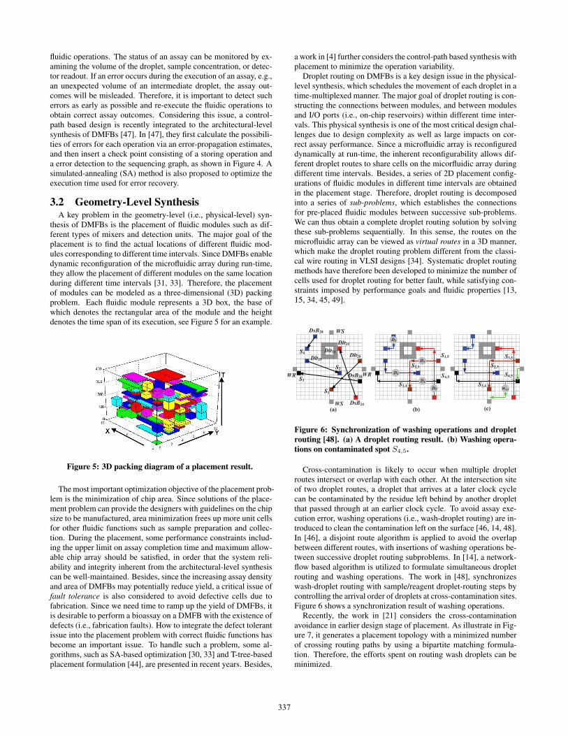
Figure 6: Synchronization of washing operations and dropletrouting [48]. (a) A droplet routing result. (b) Washing opera-tions on contaminated spot S4,5.
Cross-contamination is likely to occur when multiple dropletroutes intersect or overlap with each other. At the intersection siteof two droplet routes, a droplet that arrives at a later clock cyclecan be contaminated by the residue left behind by another dropletthat passed through at an earlier clock cycle. To avoid assay exe-cution error, washing operations (i.e., wash-droplet routing) are in-troduced to clean the contamination left on the surface [46, 14, 48].In [46], a disjoint route algorithm is applied to avoid the overlapbetween different routes, with insertions of washing operations be-tween successive droplet routing subproblems. In [14], a network-flow based algorithm is utilized to formulate simultaneous dropletrouting and washing operations. The work in [48], synchronizeswash-droplet routing with sample/reagent droplet-routing steps bycontrolling the arrival order of droplets at cross-contamination sites.Figure 6 shows a synchronization result of washing operations.
Recently, the work in [21] considers the cross-contaminationavoidance in earlier design stage of placement. As illustrate in Fig-ure 7, it generates a placement topology with a minimized numberof crossing routing paths by using a bipartite matching formula-tion. Therefore, the efforts spent on routing wash droplets can beminimized.
337

Device
A B
C D
Dispensing Port
Connectivity(Routing Path)
(b)
A D
C B
(a)
s pp
r r
q
q s
Figure 7: Different placement topology leads to different num-bers of crossing routing paths [21]. (a) Zero crossing routingpath. (b) One crossing routing path.
4. CHIP-LEVEL DESIGNIn this section, we discuss chip-level design, which consists of
electrode addressing and wire routing 1, as shown in Figure 3(d)-(f). We first show the EWOD actuator of digital microfluidics andthen discuss the electrode addressing and wire routing.
4.1 Architecture and Design Model of EWODChips
In performing various fluidic-handling functions, a primary is-sue is the manipulation of droplets. Although droplets can be con-trolled on many driving platforms [32], the EWOD chips, also re-ferred to as EWOD actuators, have received much more attentiondue to their high accuracy and efficiency, and simple fabrication [10].The EWOD chip generates electric potential by actuating electrodesto change the wettability of droplets, such that droplets can beshaped and driven along the active electrodes [25, 28]. To in-duce enough change of wettability for droplet motion, the voltagevalue applied to electrodes must exceed a threshold. This phe-nomenon enables a binary value (i.e., 1/0) to represent a relativelogic-high/logic-low value of an actuation voltage, and thus the en-tire electrode controls can be modeled simply. Furthermore, by pat-terning electrodes to a general 2D array and adopting time-varyingactuations, many droplet-based operations (e.g., mixing and cut-ting) can be well-performed on a 2D array in a reconfigurable man-ner [32].
Electrode
Conduction wires
Electrical pads
Substrate
2D pin array
Pin(a)
(b)
Figure 8: (1) Schematic view of an EWOD chip. (2) Designmodel on a 2D pin array.
As schematically presented in Figure 8(a), the general diagramof a 2D EWOD chip contains a patterned electrode array, conduc-1Note that in chip-level design, routing refers to wire routing, which is different fromdroplet routing in the fluidic domain.
tion wires, electrical pads, and a substrate [10, 22, 28, 32]. In or-der to enable the fabrication of smaller and denser electrodes withhigh interconnect routing flexibility, a typical two-metal-layer de-sign process of EWOD chips is presented in [3, 22]. It comprisestwo metal layers of 2D electrodes patterned in the first layer andconduction wires routed in the second layer, as well as an inter-insulator of silicon dioxide for via holes patterning. Based on thisarchitecture, design model for EWOD chips can be specified to a2D pin array, in which signal plan and electrical connections be-tween these pins and electrical pads (i.e., signal ports) are estab-lished, as illustrated in Figure 8(b). As a result, the majority ofexisting efforts can be roughly grouped into two main design steps:1) electrode addressing and 2) wire routing.
4.2 Electrode AddressingElectrode addressing is a method whereby electrodes are ad-
dressed with control pins to identify input signals. Early EWOD-chip designs relied on direct addressing [10], where each electrodeis directly addressed with an independent control pin. This address-ing scheme maximizes the flexibility of electrode controls. How-ever, since the control pins are actuated by an external controllerwhich supplies a limited number of signal ports, it is infeasible toactuate a large number of control pins especially for high-densityelectrode array. For example, the controller in a recently developedchip with over 1000 electrodes for multiplex immunoassay can onlyactuate 64 control pins [1]. To comply with the limited pin-countsupply, pin-constrained design of electrode addressing has beenintroduced as a solution to this problem, which utilizes a limitednumber of pins to control a large number of electrodes in EWODchips. A promising solution, broadcast addressing, has been pre-sented in [42]. The droplet-controlling information is stored in theform of electrode actuation sequences, where each bit in a sequencerepresents a signal status (“1” (actuated), “0” (de-actuated), or “X”(don’t-care)) of the electrode at a specific time step [42]. Note thatthe don’t-care symbol “X” can be either “1” or “0” which has noimpact on scheduled fluidic controls. Examples of an electrode setand their actuation sequences are presented in Figure 9(a) and (b).
1 2
3 4
65 7 8
9 10
11 12
1 4
2 5
35 3 2
4 1
5 2
e1 e2e3 e4e6e5 e7 e8e9 e10e11 e12
Electrode
Activation Sequence
e1 e2 e3 e4 e6e5 e7 e8 e9 e10 e11 e12100XX
100XX
0100X
0100X
01001
X0100
X0100
01001
XX01X
XX01X
XXX01
XXX01
(a)
(b)
(c) Pin count: 12 (d) Pin count: 5
Figure 9: (a) Electrodes that are used for handling fluidic func-tions. (b) Scheduled fluidic functions in the form of actuationsequences. (c) Applies the direct-addressing scheme. (d) Ap-plies the broadcast-addressing scheme.
Unlike direct addressing, where each electrode is assigned byan independent control pin, broadcast addressing focuses on elec-trode grouping and control signal merging through the compatibil-ity of actuation sequences. Specifically, each electrode actuationsequence may contain several don’t care terms. By carefully re-placing these don’t care terms with “1” or “0”, multiple actuation
338

sequences can be merged to an identical outcome, which is also re-ferred to as the common compatible sequence of these electrodes.Therefore, these electrodes can be assigned by the same control pinto receive the same control signal.
Take electrodes e4 and e5 in Figure 9(b) for example. By replac-ing “X” in the actuation sequence of e4 with “1”, we can merge theactuation sequences of e4 and e5 to “01001”. Therefore, e4 ande5 can be addressed with the same control pin due to their mutu-ally compatible actuation sequences. The example in Figure 9 (c)and (d) demonstrate the direct-addressing and broadcast-addressingoutcomes, respectively. Compared with the direct-addressing resultin (c), the broadcast-addressing result in (d) significantly reducesthe required control pins from 12 to 5. This reduction requiresfewer electrical devices and connections to perform the same flu-idic functions, thus improving chip reliability as well as reducingfabrication cost [42].
e1e3 e11Result 1 Result 2Pin
Two electrode grouping results
e5 e6e9 1 e1, e10 e1, e2
2 e3, e8, e12 e3, e4, e8
e7e8 e10 3 e6, e7 e6, e7
4 e2, e9 e9, e10
5e2e4 e12(a)
5 e4, e5, e11 e5, e11, e12
(b)
e1e3
e5 e6e9
e11 e1e3
e e6e9
e11
e5 e6
e7e8
e9
e10
e5 e6
ee8
e9
e10
e2e4
e7e8 e10
e12 e2e4
e7e8 e10
e12(c) Clique-partition outcome of result 1 (d) Clique-partition outcome of result 2
Figure 10: (a) A compatibility graph Gc derived from Figure9(b). (b) Two possible electrode grouping results. (c)-(d) Cor-responding clique-partition results of (b).
Researchers have utilized the compatibility graph to specify thebroadcast addressing [42], where the vertex set represents the elec-trode set and an edge between two electrodes indicates their corre-sponding activation sequences are compatible. For example, Fig-ure 10(a) demonstrates a compatibility graph Gc derived from Fig-ure 9(b). Based on the compatibility graph, the electrode groupingcan be mapped to the clique partition problem, which is a well-known example of an intractable problem in graph theory. Sinceeach clique represents an electrode group with mutually compati-ble control signals, we can individually assign each clique with adedicated control pin. Two feasible electrode grouping results canbe shown in Figure 10(b), with corresponding clique-partition re-sults in Figure 10(c)-(d). Accordingly, by recognizing a minimumclique partition in the compatibility graph, the required number ofcontrol pins can be optimally minimized. However, the generalminimum clique partition is known to be NP-hard [11] and thus iscomputationally expensive.
To tackle the computational cost, many heuristics have been pro-posed in the literature [39, 42, 43]. The work by [39] proposesan array-partition based method to group the electrode set withoutintroducing unexpected fluidic-level behaviors. The work by [42]presents a greedy method of iterative clique recognitions with max-imum cardinality on the compatibility graph. Recent work by [43]applies a connect-5 algorithm to group the electrode set with max-
Figure 11: Categorization of electrodes corresponding to dif-ferent pin-count demand [20].
imum controlling freedom of a single droplet. Moreover, severalworks further integrates various pin-count saving techniques intofluidic-level synthesis to achieve design convergence, thereby facil-itating pin-count reduction effectively [15, 49]. Moreover, a workin [20] proposes a dedicated pin-count aware design methodologyand explores the properties that are favorable for pin-count reduc-tion along the fluidic-level synthesis. It classifies the usage of elec-trodes into three categories of reaction, branching, and routing cor-responding to the design steps of resource binding, placement, anddroplet routing. ILP-based pin-count saving formulations are ap-plied to these three design steps, respectively.
1 2 3 4 5
6 7 8 10
11 12 13 14 15
16 17 19 20
3
5
1
6
1
4
2
7
2
6
3
3 4
1
4 7
1 2
Pin-constrained design
Broadcast addressing
5
5
9
18
Control pins Redundant actuations
(a) Pin count: 20 (b) Pin count: 7
Figure 12: (a) A direct-addressing result uses two pins (pin 10and pin 19) to generate two exact actuations for moving thetwo droplets. (b) A broadcast-addressing result uses one pin(pin 1) to generate two exact actuations, plus two redundantactuations, for moving the two droplets.
Although broadcast addressing serves as a promising solution topin-constrained designs, yet the redundant actuations during sig-nal merging have potentially caused a power-consumption prob-lem. For example, in Figure 12(a), the direct-addressing resultneeds two exact actuations for moving the two droplets. In Fig-ure 12(b), after applying the broadcast addressing, the pin countis greatly reduced from 20 to 7. Nevertheless, the addressing re-sult needs two exact actuations, plus two redundant actuations, formoving the two droplets. As electrodes are controlled in a se-ries of actuation steps, if control pins are not carefully assignedto electrodes, the addressing result will introduce a great numberof redundant actuations. Hence, executing a bioassay may incur ahigh power-consumption problem which is critical to many battery-driven hand-held applications. Regarding this power-consumptionproblem, one work has been recently proposed to deal with thepower-consumption problem incurred from the pin-constrained de-sign [17]. The work in [17] formulates the electrode addressing andpower saving into an effective minimum-cost maximum-flow net-work, with a progressive electrode-addressing scheme for reducingdesign complexity.
4.3 Wire RoutingAfter electrodes are addressed with control pins, conduction wires
must be appropriately routed to establish the correspondence be-tween the control pins (i.e., electrodes with the same pin must bewired together) and the signal pads with a total minimum wire-length. Since signal pads of EWOD chips generally locate outside
339

the component (defined as the 2D pin array) boundary the routingproblem that connects these inside terminal pins to outsides signalports is similar to the typical escape routing problem appearing inmany VLSI designs [5]. However, in pin-constrained EWOD-chipdesigns, multiple electrodes may share the same control pin andtherefore a single control signal may actuate multi-terminal pins.To realize the electrical connections, multi-terminal pins with thesame control signal must be routed together, and then escape to thecomponent boundary. This feature makes the typical escape router,which is based on the connection of two-terminal pins, unsuitablefor the EWOD-chip routing problem. However, readily availableCAD tools targeting this type of routing problem are still criticallylacking.
Regarding the pin-constrained design, a critical problem comesfrom the interdependence of broadcast addressing and routing. Dif-ferent broadcast-addressing results lead to different wiring connec-tions and this problem occurs even with the same pin count. Ifbroadcast addressing and routing cannot be considered together,the feasibility and quality of the routing solution may be inevitablylimited.
1 4
25
33
4
25
1
5 2
1 1
2 2
35 3 2
4 4
5 5
Conduction wire
Control pin(a) Infeasible routig solution (b) Feasible routing solution
Crossing wire
Figure 13: Consideration of electrode addressing and routing:(a) separately; (b) simultaneously.
For example, Figure 13 illustrates two routing solutions undertwo different design methods that perform the same fluidic controls(the corresponding electrode groups and addressing results can re-fer to the result 1 and result 2 in Figure 10(b), respectively). In(a), the separate consideration of electrode addressing and rout-ing confronts many back detours for pins 3-4, and thus blocks therouting for pin 5. On the other hand, in (b), simultaneous con-sideration of electrode addressing and routing provides a higherfeasibility and quality routing solution in terms of routability andwirelength. In the case of (a), additional post processes such aselectrode readdressing and rerouting or even a multi-layer routingstructure should be considered. Regarding this, an effective designto low-cost manufacturing of electrical connections cannot be real-ized [10].
There is only one existing work proposed in [15] that considersthe automated design of EWOD-chip routing. The work by [15] si-multaneously solves the electrode addressing and routing by adopt-ing a two-stage technique of global routing followed by progres-sive routing. In global routing, a set of horizontal/vertical globalrouting tracks is constructed using a maximum-flow formulation.By guiding straight routes on these tracks, the pin count and wire-length can be simultaneously minimized in a global view. Then, theprogressive routing iteratively completes the addressing and rout-ing with respect to these tracks using a minimum-cost maximum-flow model, while maintaining a minimum growth of pin count andwirelength between successive iterations.
5. TESTING AND FAULT MODELSIn this section, we describe recent advances in the testing of dig-
ital microfluidic biochips and fault localization techniques.
5.1 Fault ModelingAs in microelectronic circuits, a defective DMFB is said to have
a failure if its operation does not match its specified behavior. In or-der to facilitate the detection of defects, fault models that efficientlyrepresent the effect of physical defects at some level of abstractionare required. Faults in digital microfluidic systems can be classifiedas being either catastrophic or parametric. Catastrophic faults leadto a complete malfunction of the system, while parametric faultscause degradation in the system performance. A parametric faultis detectable only if this deviation exceeds the tolerance in systemperformance.
Table I lists some common failure sources, defects and the corre-sponding fault models for catastrophic faults in DMFB. Examplesof some common parametric faults include the following:
• Geometrical parameter deviation: The deviation in insulatorthickness, electrode length and height between parallel platesmay exceed their tolerance value.
• Change in viscosity of droplet and filler medium. These canoccur during operation due to an unexpected biochemical re-action, or changes in operational environment, e.g., tempera-ture variation.
5.2 Structure Test TechniquesA unified test methodology for DMBF has been presented, where-
by faults can be detected by controlling and tracking droplet motionelectrically [35]. Test stimuli droplets containing a conductive fluid(e.g., KCL solution) are dispensed from the droplet source. Thesedroplets are guided through the unit cells following the test plan to-wards the droplet sink, which is connected to an integrated capaci-tive detection circuit. Most catastrophic faults result in a completecessation of droplet transportation. Therefore, we can determinethe fault-free or faulty status of the system by simply observing thearrival of test stimuli droplets at selected ports. An efficient testplan ensures that testing does not conflict with the normal bioassay,and it guides test stimuli droplets to cover all the unit cells availablefor testing. The microfluidic array can be modeled as an undirectedgraph, and the pathway for the test droplet can be determined bysolving the Hamiltonian path problem [36]. With negligible hard-ware overhead, this method also offers an opportunity to imple-ment self-test for microfluidic systems and therefore eliminate theneed for costly, bulky, and expensive external test equipment. Fur-thermore, after detection, droplet flow paths for bioassays can bereconfigured dynamically such that faulty unit cells are bypassedwithout interrupting the normal operation.
Even though most catastrophic faults lead to a complete cessa-tion of droplet transportation, there exist differences between theircorresponding erroneous behaviors. For instance, to test for theelectrode-open fault, it is sufficient to move a test droplet from anyadjacent cell to the faulty cell. The droplet will always be stuck dur-ing its motion due to the failure in charging the control electrode.On the other hand, if we move a test droplet across the faulty cellsaffected by an electrode-short fault, the test droplet may or may notbe stuck depending on its flow direction. Therefore, to detect suchfaults, it is not enough to solve only the Hamiltonian path problem.In [37], a solution based on Euler paths in graphs is described fordetecting electrode shorts.
Despite its effectiveness for detecting electrode shorts, testingbased on an Euler path suffers from long test application time. This
340

TABLE I: EXAMPLES OF FAULT MODELS FOR DIGITAL MICROFLUIDIC BIOCHIP
Cause of defect Defect typeNumberof cells
Fault model Observable error
Excessive actuation voltage applied to an Dielectric breakdown 1 Droplet-electrode short (a short
between the droplet and the electrode)Droplet undergoes electrolysis, which prevents its further transportationelectrode between the droplet and the electrode) prevents its further transportation
Electrode actuation for excessive duration
Irreversible charge concentration on an electrode
1 Electrode-stuck-on (the electrode remains constantly activated)
Unintentional droplet operations or stuck droplets
Misalignment of Excessive mechanical force applied to the chip
gparallel plates (electrodes and ground plane)
1 Pressure gradient (net static pressure in some direction)
Droplet transportation without activation voltage
Coating failure Non-uniform dielectric layer 1 Dielectric islands (islands of Teflon
coating)Fragmentation of droplets and their motion is preventeddielectric layer coating) motion is prevented
Abnormal metal layer deposition and etch variation during
Grounding Failure 1 Floating droplets (droplet are not anchored ) Failure of droplet transportation
Broken wire to control source 1 Electrode open (electrode actuation is
not possible)Failure to activate the electrode for droplet transportationvariation during
fabrication Metal connection between two adjacent electrodes
2 Electrode short (short between electrodes) A droplet resides in the middle of the
two shorted electrodes, and its transport along one or moreA particle that transport along one or moredirections cannot be achievedParticle contamination or
liquid residue
A particle thatconnect two adjacent electrodes
2 Electrode short
Protein adsorption during Sample residue onResistive open at electrode Droplet transportation is impeded.
Protein adsorption duringbioassay [10]
Sample residue onelectrode surface 1
Contamination Assay results are outside the range of possible outcomes
approach uses only one droplet to traverse the microfluidic array,irrespectively of the array size. Fault diagnosis is carried out by us-ing multiple test application steps and adaptive Euler paths. Sucha diagnosis method is inefficient since defect-free cells are testedmultiple times. Moreover, the test method leads to a test plan thatis specific to a target biochip. If the array dimensions are changed,the test plan must be completely altered. In addition, to facilitatechip testing in the field, test plans need to be programmed into amicrocontroller. However, the hardware implementations of testplans from [35] are expensive, especially for low cost, disposablebiochips. More recently, a cost-effective testing methodology re-ferred to as "parallel scan-like test" has been proposed [40]. Themethod is named thus because it manipulates multiple test dropletsin parallel to traverse the target microfluidic array, just as test stim-uli can be applied in parallel to the different scan chains in an inte-grated circuit.
A drawback of the above “structural” test methods is that theyfocus only on physical defects, and they overlook module function-ality. Therefore, these methods can only guarantee that a biochip isdefect-free. However, a defect-free microfluidic array can also mal-function in many ways. For example, a defect-free reservoir mayresult in large volume variations when droplets are dispensed fromit. A splitter composed of three defect-free electrodes may splita big droplet into two droplets with significantly unbalanced vol-umes. These phenomena, referred to as malfunctions, are not theresult of electrode defects. Instead, they are activated only for cer-tain patterns of droplet movement or fluidic operations. Such mal-functions can have serious consequences on the integrity of bioas-say results.
5.3 Functional Test TechniquesFunctional testing involves test procedures to check whether gro-
ups of cells can be used to perform certain operations, e.g., dropletmixing and splitting. For the test of a specific operation, the corre-sponding patterns of droplet movement are carried out on the targetcluster of cells. If a target cell cluster fails the test, e.g., the mixing
test, we label it as a malfunctioning cluster. As in the case of struc-tural testing, fault models must be developed for functional testing.Malfunctions in fluidic operations are identified and included in thelist of faults; see Table II.
Functional test methods to detect defects and malfunctions havebeen developed. In particular, dispensing test, mixing test, split-ting test, and capacitive sensing test have been described in [41] toaddress the corresponding malfunctions.
Functional test methods were applied to a PCB microfluidic plat-form for the Polymerase Chain Reaction (PCR). The platform con-sists of two columns and two rows of electrodes, three reservoirs,and routing electrodes that connect the reservoirs to the array. Anillustration of the mixing and splitting test is shown in Figure 14.The bottom row was first targeted and five test droplets were dis-pensed to the odd electrodes, as shown in Figure 14(a). Next, split-ting test for the even electrodes was carried out. Droplets weresplit and merged on the even electrodes. In Figure 14(b), we seea series of droplets of the same volume resting on the even elec-trodes, which means that all the odd electrodes passed the splittingtest, and merging at the even electrodes worked well. However,when the splitting test was carried out on the even electrodes, alarge variation in droplet volume was observed on the 3rd and 5thelectrodes; see Figure 14(c). This variation implied a malfunction,leading to unbalanced splitting on the 4th electrode. The malfunc-tion was detected when the droplets were routed to the capacitivesensing circuit. The 4th electrode on the bottom row was markedas an unqualified splitting site.
Recently, the design of microfluidic logic gates implementingBoolean functions such as AND, OR, and NOT has been reported[50]. Logic values “0” or “1” are defined as follows: the presence(absence) of a droplet of 1x volume at an input or output port in-dicates a logic value of “1” (“0”). Unlike other microfluidic logicdesigns [24, 26], the same interpretations at inputs and outputs en-sure that logic gates can be easily cascaded. A 2-input OR gate (Z= X1+X2) is shown in Figure 15. A detector can be placed at Elec-trode 9 to determine the output value. Such capacitive or optical
341

TABLE II: FUNCTIONAL FAULT MODELS
Cause of malfunction Malfunction type Number of Fault model Observable errorCause of malfunction Malfunction type cells Fault model Observable error
Electrode actuation for excessive duration
Irreversible charge concentration on the dispensing electrode
3Dispensing-stuck-on (droplet is dispensed by not fully cut off from the reservoir)
No droplet can be dispensed from the reservoir
Electrode shape variation No overlap between droplets toElectrode shape variationin fabrication Deformity of electrodes 3 No overlap between droplets to
be mixed and center electrode Mixing failure
Electrode electrostatic property variation in fabrication
Unequal actuation voltages 3 Pressure gradient (net static
pressure in some direction)Unbalanced volumes of split droplets
Bad solderingParasitic capacitance in the capacitive sensing circuit
1 Oversensitive or insensitive capacitive sensing
False positive/negative in detection
1 2 3 4 5 6 7 8 9
(a)
1 2 3 4 5 6 7 8 9
(b)
1 2 3 4 5 6 7 8 91 2 3 4 5 6 7 8 9
Malfunction (unbalanced splitting)
(c)
Figure 14: Mixing and splitting test for a fabricated PCR chip.
detectors to indicate the presence of a droplet can be easily imple-mented [50]. The sequence of control voltages is independent ofthe input logic values, which allows easy implementation. Suchlogic gates have been used for the design of response compactorsfor built-in self-test.
Figure 15: A microfluidic OR gate.
6. FUTURE DESIGN CHALLENGESFuture design challenges lie in the incorporation of chip relia-
bility into the CAD flow of DMFB. One significant problem is thereliability problem incurred from pin-constrained designs. Control-pin/-signal sharing might introduce additional and unnecessary elec-
trode actuations, which has the potential to make an electrode con-front excessive actuations in case of a naive design. Studies onEWOD chips have reported this kind of problem accelerates theextent of trapping charge, leading to a permanent degradation ofdielectric layer [9, 18, 38]. This scenario inevitably impedes com-plete and correct fluidic controls and therefore degrades the chipreliability. Thus, it becomes desirable and crucial to strike a bal-ance between control-pin/-signal sharing and reliability preserva-tion when the chip size and assay functionality grow, especiallyunder the circumstance of pin-constrained design.
Reliability-aware placement needs to be incorporated. Currentdesign automations place the modules with unrestricted sharing ofcells/electrodes to minimize the chip size. For some applicationssuch as point-of-care testing, on-chip fluidic modules, for examplethe fluidic modules of incubations, are associated with relativelylong execution durations than other counterparts such as simplemixing and dilution. If cells are overly shared by these modules,the underlying electrodes many suffer from excessive actuationsthereby decreasing the lifetime of electrodes, which degrades thechip reliability. Therefore, it is desirable to develop a reliability-aware placement algorithm for this kind of applications.
Optimization across energy domains also needs to be investi-gated. Such optimization problems that span several energy do-mains (e.g., electrical, circuit, fluidic, and thermal domains) appearto be extremely difficult due to the further involvements of energy-related constraints or objectives. For example, in pin-constraineddesign, we should limit the fanout of a single control pin to avoidoverly charge sharing, which might cause problems such as highpower dissipation and trapped charge. Moreover, thermal-awaresignal planning is also important for the prevention of fluidics fromoverheating in some area that has congested electrical connections.
Biochip operation execution is in the order of seconds, whereasspecialized heuristics for the synthesis problems can potentially ob-tain good results in milliseconds [27]. An interesting possibility inthis context is to perform the synthesis online, while the biochem-ical application is running, and not offline, as it has been done sofar. Such an online approach has the advantage of adaptivity, tofaults in the architecture or variations in the operation execution. Inaddition, it opens up the possibility of fully portable point-of-caredevices. Although no research has been done so far in this area,recent research [4, 47] has shown how an implementation can reactto faults by switching online to recovery schedules pre-synthesizedoffline.
7. CONCLUSIONSIn this paper, we have provided a survey on recent research in
the design and optimization of DMFBs. We show how CAD toolsare involved to automate the design of DMFBs. Several optimiza-tion problems appearing in the design stages, fluidic-level synthe-
342

sis, chip-level design, and testing, are also presented. In addition,we have pointed out a set of open problems and design challengesthat remain to be tackled in the future. The authors believe thispaper will spark more research interests being devoted into the de-velopments of CAD tools for DMFBs, which are expected to pavethe way for the deployment and use of biochips in the emergingmarketplace.
8. ACKNOWLEDGEMENTSThis work was partially supported by the National Science Coun-
cil of Taiwan ROC under Grant No. NSC 100-2220-E-006-016, inpart by the US National Science Foundation under grant no. CCF-0914895, and in part by the EU ArtistDesign Network of Excel-lence on Embedded Systems Design and by the Danish Agencyfor Science, Technology and Innovation, Grant No. 2106-08-0018“ProCell”.
9. REFERENCES[1] Advanced Liquid Logic, Inc., http://www.liquid-logic.com.[2] Nanotechnology News, http://www.nanotech-now.com/.[3] Microfluidic Lab., Duke University, http://microfluidics.ee.duke.edu/[4] M. Alistar, E. Maftei, P. Pop, and J. Madsen, “Synthesis of biochemical
applications on digital microfluidic biochips with operation variability,” Proc.DTIP, pp. 350–357, 2010.
[5] C. J. Alpert, D. P. Mehta, S. S. Sapatnekar, “Handbook of Algorithms forPhysical Design Automation,” CRC Press, 2009.
[6] K. Chakrabarty, “Towards fault-tolerant digital microfluidic lab-on-chip:defects, fault modeling, testing, and reconfiguration,” Proc. IEEE ICBCS, pp.329–332, 2008.
[7] K. Chakrabarty, “Design automation and test solutions for digital microfluidicbiochips,” IEEE Trans. CAS I, vol. 57, pp. 4–17, 2010.
[8] M. Cho and D. Z. Pan, “A high-performance droplet routing algorithm fordigital microfluidic biochips,” IEEE Trans. on CAD, vol. 27, no. 10, pp.1714–1724, 2008.
[9] A. I. Drygiannakis, A. G. Papathanasiou, and A. G. Boudouvis, “On theconnection between dielectric breakdown strength, trapping of charge, andcontact angle saturation in electrowetting,” ACS J. Langmuir, no. 25, pp.147–152, 2009.
[10] J. Gong and C. J. Kim, “Direct-referencing two-dimensional-array digitalmicrofluidics using multilayer printed circuit board,” IEEE J. MEMS, no. 2,pp. 257–264, 2008.
[11] J. L. Gross, and J. Yellen, “Graph Theory and Its Application,” CRC Press,FL, 1999.
[12] T.-Y. Ho, J. Zeng, and K. Chakrabarty, “Digital microfluidic biochips: Avision for functional diversity and more than Moore,” Proc. IEEE/ACMICCAD, pp. 578–585, 2010.
[13] T.-W. Huang and T.-Y. Ho, “A fast routability- and performance-driven dropletrouting algorithm for digital microfluidic biochips,” IEEE ICCD, pp. 445–450,2009.
[14] T.-W. Huang, C.-H. Lin, and T.-Y. Ho, “A contamination aware droplet routingalgorithm for digital microfluidic biochips,” IEEE/ACM ICCAD, pp. 151–156,2009.
[15] T.-W. Huang and T.-Y. Ho, “A two-stage ILP-based droplet routing forpin-constrained digital microfluidic biochips,” Proc. ACM ISPD, pp. 201–208,2010
[16] T.-W. Huang, S.-Y. Yeh, and T.-Y. Ho, “A network-flow based pin-count awarerouting algorithm for broadcast electrode-addressing EWOD chips,” Proc.IEEE/ACM ICCAD, pp. 425–431, 2010
[17] T.-W. Huang, H.-Y. Su, and T.-Y. Ho, “Progressive network-flow basedpower-aware broadcast addressing for pin-constrained digital microfluidicbiochips,” Proc. ACM/IEEE DAC, 2011
[18] A. Kerber, F. Cartier, R. Degraeve, P. J. Roussel, L. Pantisano, T. Kauerauf, G.Groeseneken, H. E. Maes, and U. Schwalke, “Charge trapping and dielectricreliability of SiO2-Al2O3 gate stacks with TiN electrodes,” IEEE Trans. onElectron Devices, no. 50, pp. 1261–1269, 2003.
[19] K. Chakrabarty, R. B. Fair, and J. Zeng, “Design tools for digital microfluidicbiochips: Towards functional diversification and more than Moore,” IEEETrans. on CAD, vol. 29, pp. 1001-1017, July 2010.
[20] C. C.-Y. Lin and Y.-W. Chang, “ILP-based pin-count aware designmethodology for microfluidic biochips,” Proc. ACM/IEEE DAC, pp. 258–263,2009.
[21] C. C.-Y. Lin and Y.-W. Chang, “Cross-contamination aware designmethodology for pin-constrained digital microfluidic biochips,” Proc.ACM/IEEE DAC, 2010.
[22] Y.-Y. Lin, R. D. Evans, E. Welch, B.N. Hsu, A. C. Madison, and R. B. Fair,“Low Voltage Electrowetting-on-Dielectric Platform using Multi-LayerInsulators,” Sensors and Actuators B: Chemical, pp. 465–470, 2010.
[23] E. Maftei, P. Paul, and J. Madsen, “Tabu search-based synthesis ofdynamically reconfigurable digital microfluidic biochips,” ACM CASES, pp.195–203, 2009.
[24] D. W. M. Marr and T. Munakata, “Micro/nanofluidic computing,” Commun.ACM, vol. 50, pp. 64–68, 2007.
[25] M. G. Pollack, A. D. Shenderov, and R. B. Fair, “Electrowetting-basedactuation of droplets for integrated microfluidics,” LOC, pp. 96–101, 2002.
[26] M. Prakash and N. Gershenfeld, “Microfluidic bubble logic,” Science, vol.315, pp. 832–835, 2007.
[27] Christian Ejdal Sjøgreen, “Synthesis of Biochemical Applications withOperation Variability on Digital Microfluidic Biochips,” Bachelor Thesis,Technical University of Denmark, 2011.
[28] J. H. Song, R. Evans, Y. Y. Lin, B. N. Hsu, and R. B. Fair, “A scaling modelfor electrowetting-on-dielectric microfluidic actuators,” Microfluidics andNanofluidics, pp. 75–89, 2009.
[29] F. Su and K. Chakrabarty, “Architectural-level synthesis of digitalmicrofluidics-based biochips,” Proc. IEEE/ACM ICCAD, pp. 223–228, 2004.
[30] F. Su and K. Chakrabarty, “Unified high-level synthesis and module placementfor defect-tolerant microfluidic biochips,” IEEE/ACM DAC, pp. 825–830,2005.
[31] F. Su and K. Chakrabarty, “Reconfiguration techniques for digital microfluidicbiochips,” IEEE DTIP, pp. 143–148, 2005.
[32] F. Su, K. Chakrabarty, and R. B. Fair, “Microfluidics based biochips:Technology issues, implementation platforms, and design-automationchallenges,” IEEE Trans. on CAD, pp. 211–223, 2006.
[33] F. Su and K. Chakrabarty, “Module placement for fault-tolerantmicrofluidics-based biochips,” ACM TODAES, vol. 11, pp. 682–710, 2006.
[34] F. Su, W. Hwang, and K. Chakrabarty, “Droplet routing in the synthesis ofdigital microfluidic biochips,” IEEE/ACM DATE, pp. 1–6, 2006.
[35] F. Su, S. Ozev and K. Chakrabarty, “Ensuring the operational health ofdroplet-based microelectrofluidic biosensor systems”, IEEE Sensors, vol. 5,pp. 763–773, 2005.
[36] F. Su, S. Ozev and K. Chakrabarty, “Test planning and test resourceoptimization for droplet-based microfluidic systems”, JETTA, vol. 22, pp.199–210, 2006.
[37] F. Su, W. Hwang, A. Mukherjee and K. Chakrabarty, “Testing and diagnosis ofrealistic defects in digital microfluidic biochips”, JETTA, vol. 23, pp. 219–233,2007.
[38] H. J. J. Verheijen and M. W. J. Prins, “Reversible electrowetting and trappingof charge: model and experiments,” ACS J. Langmuir, no. 15, pp. 6616–6620,1999.
[39] T. Xu and K. Chakrabarty, “Droplet-trace-based array partitioning and a pinassignment algorithm for the automated design of digital microfluidicbiochips,” Proc. CODES+ISSS, pp. 112–117, 2006.
[40] T. Xu and K. Chakrabarty, “Parallel scan-like test and multiple-defectdiagnosis for digital microfluidic biochips”, IEEE Trans. BioCAS, vol. 1, pp.148–158, 2007.
[41] T. Xu and K. Chakrabarty, “Functional testing of digital microfluidicbiochips”, IEEE ITC, 2007.
[42] T. Xu and K. Chakrabarty, “Broadcast electrode-addressing forpin-constrained multi-functional digital microfluidic biochips,” Proc.IEEE/ACM DAC, pp. 173–178, 2008.
[43] T. Xu, K. Chakrabarty and V. K. Pamula, “Defect-tolerant design andoptimization of a digital microfluidic biochip for protein crystallization,” IEEETrans. on CAD, 2010.
[44] P.-H. Yuh, C.-L. Yang, and Y.-W. Chang, “Placement of defect-tolerant digitalmicrofluidic biochips using the T-tree formulation,” ACM JETC, vol. 3, no. 3,2007.
[45] P.-H. Yuh, C.-L. Yang, and Y.-W. Chang, “BioRoute: A network flow basedrouting algorithm for the synthesis of digital microfluidic biochips,” IEEETrans. on CAD, vol. 27, no. 11, pp. 1928–1941, 2008.
[46] Y. Zhao and K. Chakrabarty, “Cross-contamination avoidance for dropletrouting in digital micro fluidic biochips,” IEEE/ACM DATE, pp. 1290–1295,2009.
[47] Y. Zhao, T. Xu and K. Chakrabarty, “Control-path design and error recovery indigital microfluidic lab-on-chip,” ACM JETC, vol. 3, No. 11, 2010.
[48] Y. Zhao, T. Xu and K. Chakrabarty, “Synchronization of washing operationswith droplet routing for cross-contamination avoidance in digital microfluidicbiochips,” IEEE/DAC, pp. 635–640, 2010.
[49] Y. Zhao and K. Chakrabarty, “Co-optimization of droplet routing and pinassignment in disposable digital microfluidic biochips,” Proc. ACM ISPD, pp.69–76, 2011.
[50] Y. Zhao and K. Chakrabarty, “Digital microfluidic logic gates and theirapplication to built-in self-test of lab-on-chip,” IEEE Trans. BioCAS, vol. 4,pp. 250–262, August 2010.
343