direct mounting of quartz crystal on a cmos pll chip
TRANSCRIPT

Direct Mounting of Quartz Crystal on a CMOS PLL Chip
Hyunsoo Kim*, and Tom Jackson Center for Thin Film Devices
and Materials Research Institute Department of Electrical Engineering
Penn State University University Park, USA
Jaehyun Lim, Kyusun Choi Department of Computer Science Engineering
Penn State University
Dave Kenny Eastern Development Center
Saronix
Abstract— This paper reports progress on directly mounting a quartz crystal on a CMOS oscillator and PLL chip. This approach minimizes the distance between the quartz crystal resonator and the oscillator circuitry and can allow reduced power with reduced stray coupling effects. This approach also allows simplified packaging and can reduce the volume and weight of precision oscillators.
I. INTRODUCTION Highly accurate and stable reference clocks are important
for most communication and network systems, cellular phone, wireless modem, and GPS navigation systems. For mobile systems small form factor and light weight are essential ingredients for product marketability. Motivated by these factors, we have investigated the direct mounting of quartz crystal resonators on CMOS oscillator chips.
The key pieces of our integrated chip and resonator include voltage controlled oscillators (VCO), phase locked loops (PLL), and high Q quartz crystal resonators. Mounting the quartz crystal resonator directly on chip eliminates the off-chip interface for the crystal and separate crystal packaging allowing the size of entire clock generation system to be reduced. System reliability, frequency stability, and precision may also be improved [1] [2].
In this paper, we report initial results of a crystal-on-chip low-noise/jitter voltage controlled oscillator circuit and integrated high precision PLL. To allow easy comparison to non-integrated designs, resonators with a fundamental mode frequency of 155.52 MHz were used and the integrated oscillators were compared to standard non-integrated crystal quartz crystal oscillators.
II. MOUNTING QUARTZ CRYSTAL ON CHIP The approach for integrating quartz crystals on chip is
shown in Figure 1. As shown in the Fig. 1, a 155.52 MHz AT-cut Tab Mesa type quartz crystal resonator is directly mounted on the chip in which the voltage controlled crystal oscillator (VCXO) and PLL are integrated. The quartz crystal resonator
is mounted with conductive epoxy on the chip surface and the epoxy is cured in a vacuum oven at 150 ºC for 40 minutes.
In our first prototype chip, the chip size is designed slightly larger than quartz crystal resonator so that whole quartz crystal resonator is located within the perimeter of the Si substrate. This prototype IC is 1.85 mm by 3.7 mm, however the VCXO and PLL circuits together with all digital control circuits occupy only about 10% of the total chip area.
Electrode
Quartz crystal
CMOS chip
Mounting structure
Figure 1. Quarttz crystal on-chip approach
Figure 2. Micrograph of quartz crystal resonator on CMOS chip
This work was supported in part by Pittsburgh Digital Greenhouse through a grant from the Commonwealth of Pennsylvania, Department of Community and Economic Development.
0-7803-8414-8/04/$20.00 (c)2004 IEEE. and Frequency Control Joint 50th Anniversary Conference1652004 IEEE International Ultrasonics, Ferroelectrics,

Figure 3. FR4 test board with crystal on chip
Crystal-on-chip oscillators were tested using both packaged and unpackaged ICs. Unpackaged testing allowed reduced bond wire length (and therefore bond wire inductance) compared to devices in standard IC packages. Figure 3 shows a simple FR4 board designed to mount and test unpackaged prototype crystal-on-chip oscillators.
III. VCXO AND PLL The crystal-on-chip prototype CMOS IC has integrates
VCXO, PLL, and digital control circuitry and was fabricated in 0.5 micron AMIS technology using the MOSIS service. The VCXO consists of an oscillator core, varactors, and the quartz crystal resonator. In this circuit, two varactors are used as variable capacitive loads to provide frequency control (Fig. 4) [3]. Two complete oscillators are included on the prototype IC to allow signal coupling to be investigated (Fig. 5).
The PLL reference frequency divider (RFD) and output frequency divider (OFD) are designed using T-flipflops. A 16 kHz external reference signal is applied to the RFD and its output, either an 8 kHz or 16 kHz signal, is fed into a phase frequency detector (PFD). The 155.52 MHz clock from the voltage controlled crystal oscillator (VCXO) is divided by the OFD and the output, which is also fed into the PFD, is selected as 77.76 MHz, 38.88 MHz, 19.44 MHz, 32 kHz, 16 kHz, or 8 kHz [4].
C3
C4
Vdd
VcR2
C2
C1
Vdd
VcR1
R3
Figure 4. VCXO circuit diagram
Figure 5. Chip layout (Oscillator cores, digital cores and resonator mounting structure)
Figure 6. The architecture of phase locked loop
Fig. 6 shows a simplified block diagram of the PLL. Signals from the RFD and OFD are compared in the PFD. Normally the frequencies of both signals will be nearly the same. The output of the phase detector indicates a relationship between two inputs [5]. An alarm module detects two cases – loss of lock (LOL), and loss of reference (LOR). An RC low pass loop filter output voltage controls the VCXO as a control voltage, with a 0V to 3.3V control range. Two PLLs are implemented on our test chip. One allows the PLL design to be thoroughly tested and has each function block output brought to a bonding pad. The second PLL is used in the active crystal oscillator.
Oscillator cores
Resonator mounting structure
Digital cores
0-7803-8414-8/04/$20.00 (c)2004 IEEE. and Frequency Control Joint 50th Anniversary Conference1662004 IEEE International Ultrasonics, Ferroelectrics,
REF 9.6 dBm MKR 155.8 MHz4.78 dBm
START 10 MHz STOP 500 MHzRES BW 3.0 MHz VBW 3.0 MHz SWP 20 msec
PEAK
LOG
10 dB/
REF 9.6 dBm MKR 155.8 MHz4.78 dBm
START 10 MHz STOP 500 MHzRES BW 3.0 MHz VBW 3.0 MHz SWP 20 msec
PEAK
LOG
10 dB/
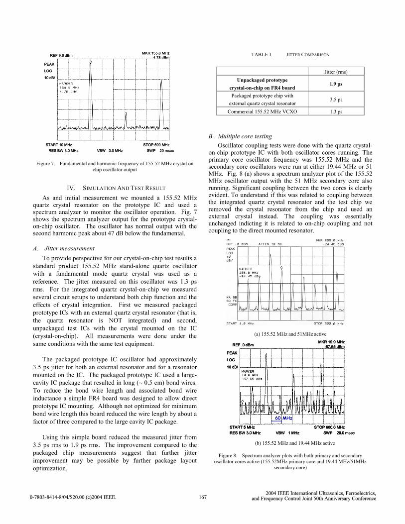
Figure 7. Fundamental and harmonic frequency of 155.52 MHz crystal on chip oscillator output
IV. SIMULATION AND TEST RESULT As and initial measurement we mounted a 155.52 MHz
quartz crystal resonator on the prototype IC and used a spectrum analyzer to monitor the oscillator operation. Fig. 7 shows the spectrum analyzer output for the prototype crystal-on-chip oscillator. The oscillator has normal output with the second harmonic peak about 47 dB below the fundamental.
A. Jitter measurement To provide perspective for our crystal-on-chip test results a
standard product 155.52 MHz stand-alone quartz oscillator with a fundamental mode quartz crystal was used as a reference. The jitter measured on this oscillator was 1.3 ps rms. For the integrated quartz crystal-on-chip we measured several circuit setups to understand both chip function and the effects of crystal integration. First we measured packaged prototype ICs with an external quartz crystal resonator (that is, the quartz resonator is NOT integrated) and second, unpackaged test ICs with the crystal mounted on the IC (crystal-on-chip). All measurements were done under the same conditions with the same test equipment.
The packaged prototype IC oscillator had approximately 3.5 ps jitter for both an external resonator and for a resonator mounted on the IC. The packaged prototype IC used a large-cavity IC package that resulted in long (~ 0.5 cm) bond wires. To reduce the bond wire length and associated bond wire inductance a simple FR4 board was designed to allow direct prototype IC mounting. Although not optimized for minimum bond wire length this board reduced the wire length by about a factor of three compared to the large cavity IC package.
Using this simple board reduced the measured jitter from 3.5 ps rms to 1.9 ps rms. The improvement compared to the packaged chip measurements suggest that further jitter improvement may be possible by further package layout optimization.
TABLE I. JITTER COMPARISON
B. Multiple core testing Oscillator coupling tests were done with the quartz crystal-
on-chip prototype IC with both oscillator cores running. The primary core oscillator frequency was 155.52 MHz and the secondary core oscillators were run at either 19.44 MHz or 51 MHz. Fig. 8 (a) shows a spectrum analyzer plot of the 155.52 MHz oscillator output with the 51 MHz secondary core also running. Significant coupling between the two cores is clearly evident. To understand if this was related to coupling between the integrated quartz crystal resonator and the test chip we removed the crystal resonator from the chip and used an external crystal instead. The coupling was essentially unchanged indicting it is related to on-chip coupling and not coupling to the direct mounted resonator.
(a) 155.52 MHz and 51MHz active
REF .0 dBmMKR 19.9 MHz
-57.65 dBm
START 5 MHz STOP 600.0 MHzRES BW 3.0 MHz VBW 1 MHz SWP 20.0 msec
PEAK
LOG
10 dB/
60 MHz
REF .0 dBmMKR 19.9 MHz
-57.65 dBm
START 5 MHz STOP 600.0 MHzRES BW 3.0 MHz VBW 1 MHz SWP 20.0 msec
PEAK
LOG
10 dB/
REF .0 dBmMKR 19.9 MHz
-57.65 dBm
START 5 MHz STOP 600.0 MHzRES BW 3.0 MHz VBW 1 MHz SWP 20.0 msec
PEAK
LOG
10 dB/
REF .0 dBmMKR 19.9 MHz
-57.65 dBm
START 5 MHz STOP 600.0 MHzRES BW 3.0 MHz VBW 1 MHz SWP 20.0 msec
PEAK
LOG
10 dB/
60 MHz
(b) 155.52 MHz and 19.44 MHz active
Figure 8. Spectrum analyzer plots with both primary and secondary oscillator cores active (155.52MHz primary core and 19.44 MHz/51MHz
secondary core)
Jitter (rms) Unpackaged prototype
crystal-on-chip on FR4 board 1.9 ps
Packaged prototype chip with external quartz crystal resonator
3.5 ps
Commercial 155.52 MHz VCXO 1.3 ps
0-7803-8414-8/04/$20.00 (c)2004 IEEE. and Frequency Control Joint 50th Anniversary Conference1672004 IEEE International Ultrasonics, Ferroelectrics,
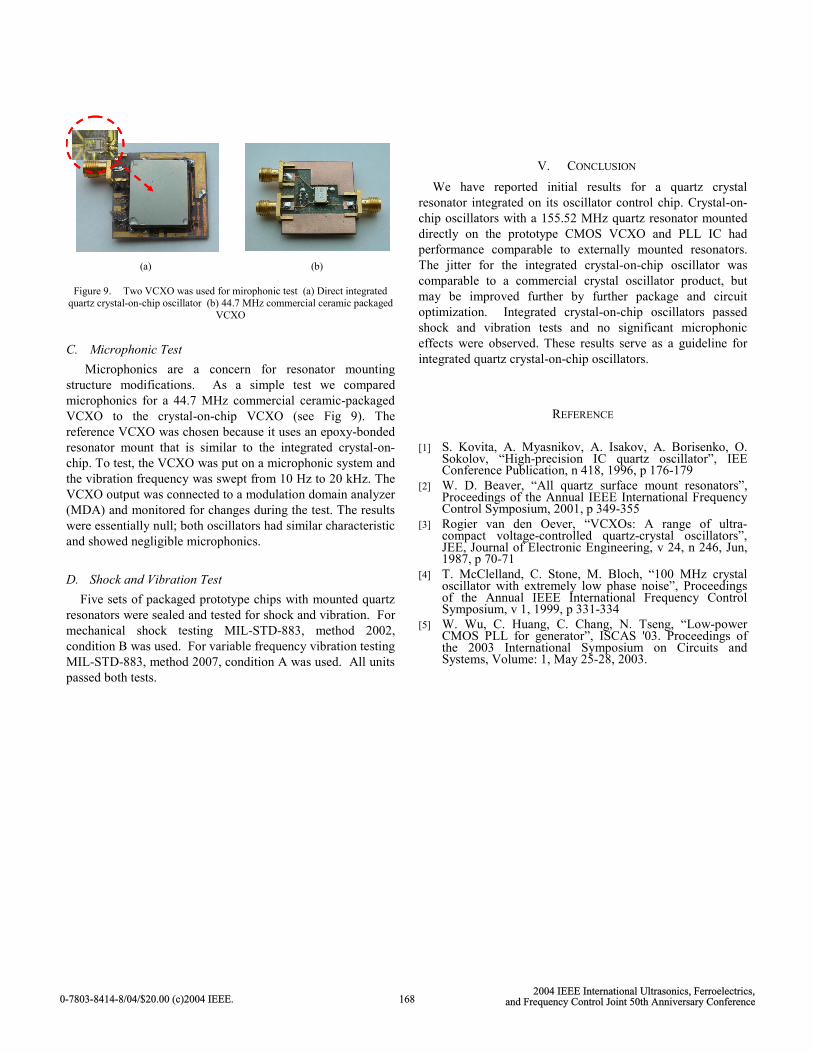
(a) (b)
Figure 9. Two VCXO was used for mirophonic test (a) Direct integrated quartz crystal-on-chip oscillator (b) 44.7 MHz commercial ceramic packaged
VCXO
C. Microphonic Test Microphonics are a concern for resonator mounting
structure modifications. As a simple test we compared microphonics for a 44.7 MHz commercial ceramic-packaged VCXO to the crystal-on-chip VCXO (see Fig 9). The reference VCXO was chosen because it uses an epoxy-bonded resonator mount that is similar to the integrated crystal-on-chip. To test, the VCXO was put on a microphonic system and the vibration frequency was swept from 10 Hz to 20 kHz. The VCXO output was connected to a modulation domain analyzer (MDA) and monitored for changes during the test. The results were essentially null; both oscillators had similar characteristic and showed negligible microphonics.
D. Shock and Vibration Test Five sets of packaged prototype chips with mounted quartz
resonators were sealed and tested for shock and vibration. For mechanical shock testing MIL-STD-883, method 2002, condition B was used. For variable frequency vibration testing MIL-STD-883, method 2007, condition A was used. All units passed both tests.
V. CONCLUSION We have reported initial results for a quartz crystal
resonator integrated on its oscillator control chip. Crystal-on-chip oscillators with a 155.52 MHz quartz resonator mounted directly on the prototype CMOS VCXO and PLL IC had performance comparable to externally mounted resonators. The jitter for the integrated crystal-on-chip oscillator was comparable to a commercial crystal oscillator product, but may be improved further by further package and circuit optimization. Integrated crystal-on-chip oscillators passed shock and vibration tests and no significant microphonic effects were observed. These results serve as a guideline for integrated quartz crystal-on-chip oscillators.
REFERENCE [1] S. Kovita, A. Myasnikov, A. Isakov, A. Borisenko, O.
Sokolov, “High-precision IC quartz oscillator”, IEE Conference Publication, n 418, 1996, p 176-179
[2] W. D. Beaver, “All quartz surface mount resonators”, Proceedings of the Annual IEEE International Frequency Control Symposium, 2001, p 349-355
[3] Rogier van den Oever, “VCXOs: A range of ultra-compact voltage-controlled quartz-crystal oscillators”, JEE, Journal of Electronic Engineering, v 24, n 246, Jun, 1987, p 70-71
[4] T. McClelland, C. Stone, M. Bloch, “100 MHz crystal oscillator with extremely low phase noise”, Proceedings of the Annual IEEE International Frequency Control Symposium, v 1, 1999, p 331-334
[5] W. Wu, C. Huang, C. Chang, N. Tseng, “Low-power CMOS PLL for generator”, ISCAS '03. Proceedings of the 2003 International Symposium on Circuits and Systems, Volume: 1, May 25-28, 2003.
0-7803-8414-8/04/$20.00 (c)2004 IEEE. and Frequency Control Joint 50th Anniversary Conference1682004 IEEE International Ultrasonics, Ferroelectrics,