a 45-nm soi-cmos dual-pll processor clock system for multi...
TRANSCRIPT
A 45-nm SOI-CMOS Dual-PLL Processor Clock System
for Multi-Protocol I/ODennis Fischette, Alvin Loke, Michael Oshima,
Bruce Doyle, Roland Bakalski*, Richard DeSantis, Anand Thiruvengadam, Charles Wang,
Gerry Talbot, Emerson Fang
Advanced Micro Devices,Inc., *GlobalFoundries
2
Outline
•• IntroductionIntroduction
• Architecture and Circuits• Ring-based PLL• LC-based PLL
• Silicon Results
• Conclusion
3
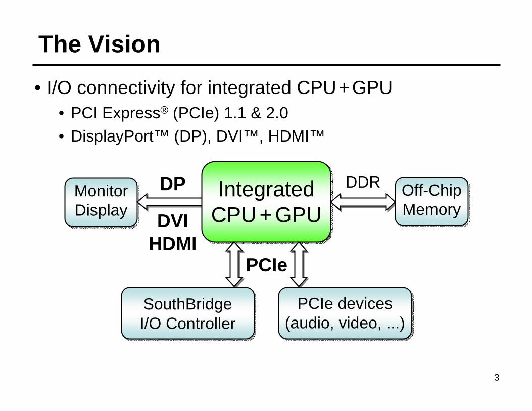
The Vision
• I/O connectivity for integrated CPU+GPU• PCI Express® (PCIe) 1.1 & 2.0• DisplayPort™ (DP), DVI™, HDMI™
MonitorDisplay
DP
DVIHDMI
PCIe
IntegratedCPU +GPU
DDR
PCIe devices(audio, video, ...)
SouthBridgeI/O Controller
Off-ChipMemory
4
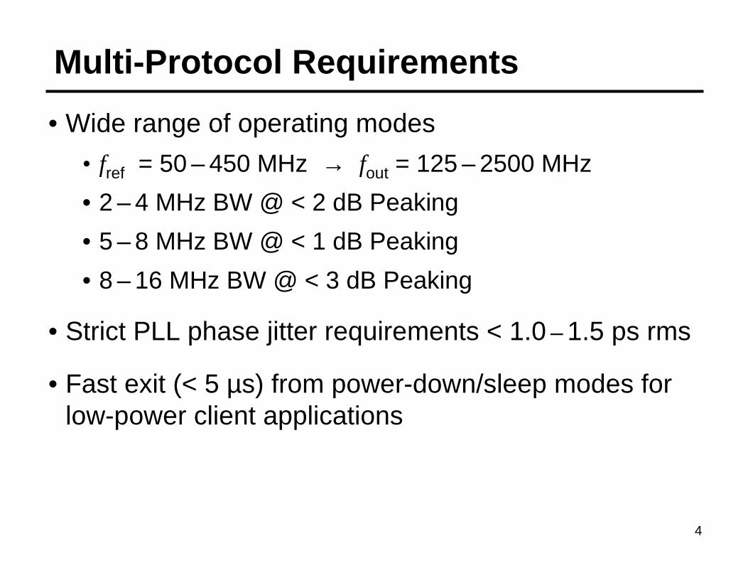
Multi-Protocol Requirements
• Wide range of operating modes
• fref = 50 – 450 MHz → fout = 125 – 2500 MHz
• 2 – 4 MHz BW @ < 2 dB Peaking
• 5 – 8 MHz BW @ < 1 dB Peaking
• 8 – 16 MHz BW @ < 3 dB Peaking
• Strict PLL phase jitter requirements < 1.0 – 1.5 ps rms
• Fast exit (< 5 µs) from power-down/sleep modes for low-power client applications
5
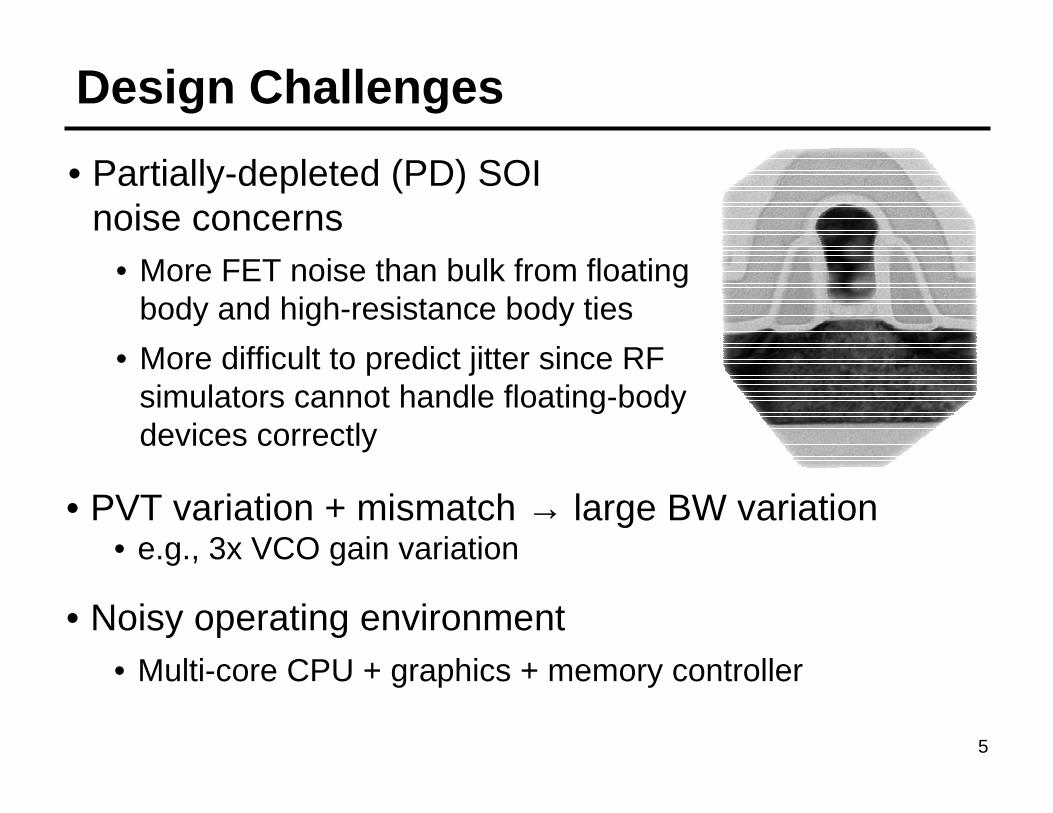
Design Challenges
• Partially-depleted (PD) SOI noise concerns
• More FET noise than bulk from floating body and high-resistance body ties
• More difficult to predict jitter since RF simulators cannot handle floating-body devices correctly
• PVT variation + mismatch → large BW variation • e.g., 3x VCO gain variation
• Noisy operating environment• Multi-core CPU + graphics + memory controller
6
Outline
• Introduction
•• Architecture and CircuitsArchitecture and Circuits•• RingRing --based PLLbased PLL•• LCLC--based PLLbased PLL
• Silicon Results
• Conclusion
7
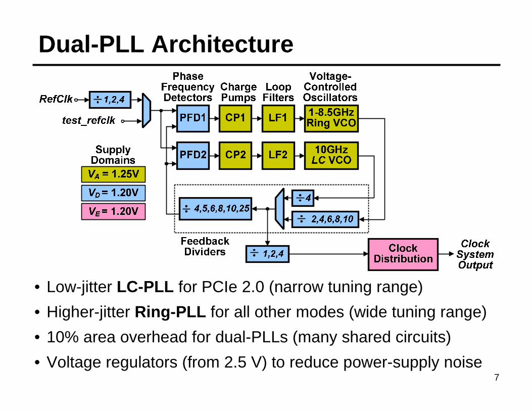
• Low-jitter LC-PLL for PCIe 2.0 (narrow tuning range)
• Higher-jitter Ring-PLL for all other modes (wide tuning range)
• 10% area overhead for dual-PLLs (many shared circuits)
• Voltage regulators (from 2.5 V) to reduce power-supply noise
Dual-PLL Architecture
8
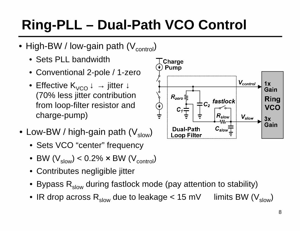
Ring-PLL – Dual-Path VCO Control• High-BW / low-gain path (Vcontrol)
• Sets PLL bandwidth
• Conventional 2-pole / 1-zero
• Effective KVCO ↓ → jitter ↓(70% less jitter contribution from loop-filter resistor and charge-pump)
• Low-BW / high-gain path (Vslow)
• Sets VCO “center” frequency
• BW (Vslow) < 0.2% ×××× BW (Vcontrol)
• Contributes negligible jitter
• Bypass Rslow during fastlock mode (pay attention to stability)
• IR drop across Rslow due to leakage < 15 mV à limits BW (Vslow)
9
0.0
0.5
1.0
1.5
2.0
2.5
0.0 1.0 2.0 3.0 4.0
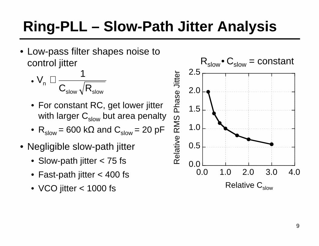
Ring-PLL – Slow-Path Jitter Analysis
• Low-pass filter shapes noise to control jitter
•
• For constant RC, get lower jitter with larger Cslow but area penalty
• Rslow = 600 k and Cslow = 20 pF
• Negligible slow-path jitter• Slow-path jitter < 75 fs
• Fast-path jitter < 400 fs
• VCO jitter < 1000 fs
slowslow
nRC
V1∝
Rslow•Cslow = constant
Relative Cslow
Rel
ativ
e R
MS
Pha
se J
itter
10
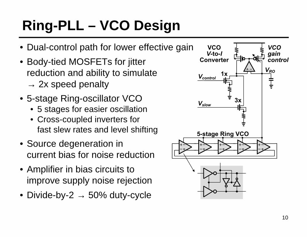
Ring-PLL – VCO Design• Dual-control path for lower effective gain
• Body-tied MOSFETs for jitter reduction and ability to simulate → 2x speed penalty
• 5-stage Ring-oscillator VCO• 5 stages for easier oscillation• Cross-coupled inverters for
fast slew rates and level shifting
• Source degeneration in current bias for noise reduction
• Amplifier in bias circuits to improve supply noise rejection
• Divide-by-2 → 50% duty-cycle
5-stage Ring VCO
1x
3x
Vcontrol
VRO
VCOgain control
Vslow
VCOV-to-I
Converter
11
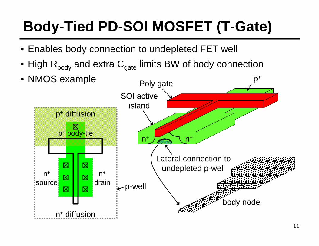
Body-Tied PD-SOI MOSFET (T-Gate) • Enables body connection to undepleted FET well
• High Rbody and extra Cgate limits BW of body connection
• NMOS example
p-well
Lateral connection toundepleted p-well
n+n+
p+
body node
p+ diffusion
n+ diffusion
p+ body-tie
n+
sourcen+
drain
SOI active island
Poly gate
12
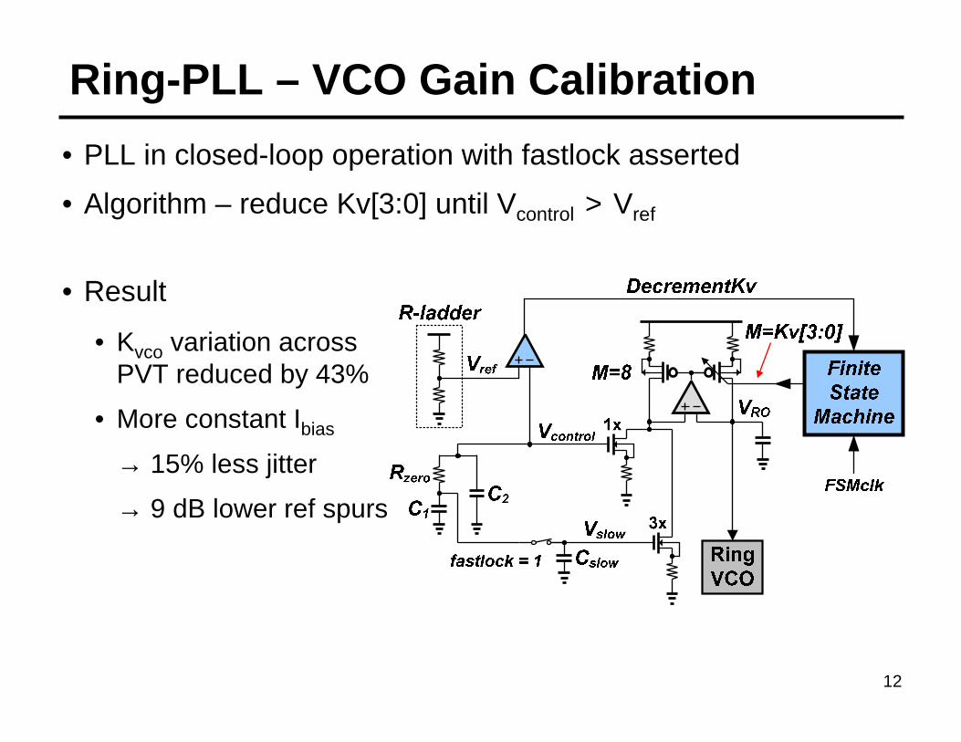
Ring-PLL – VCO Gain Calibration
• Result
• Kvco variation across PVT reduced by 43%
• More constant Ibias
→ 15% less jitter
→ 9 dB lower ref spurs
• PLL in closed-loop operation with fastlock asserted
• Algorithm – reduce Kv[3:0] until Vcontrol > Vref
13
-8
-4
0
4
8
0 1 2 3
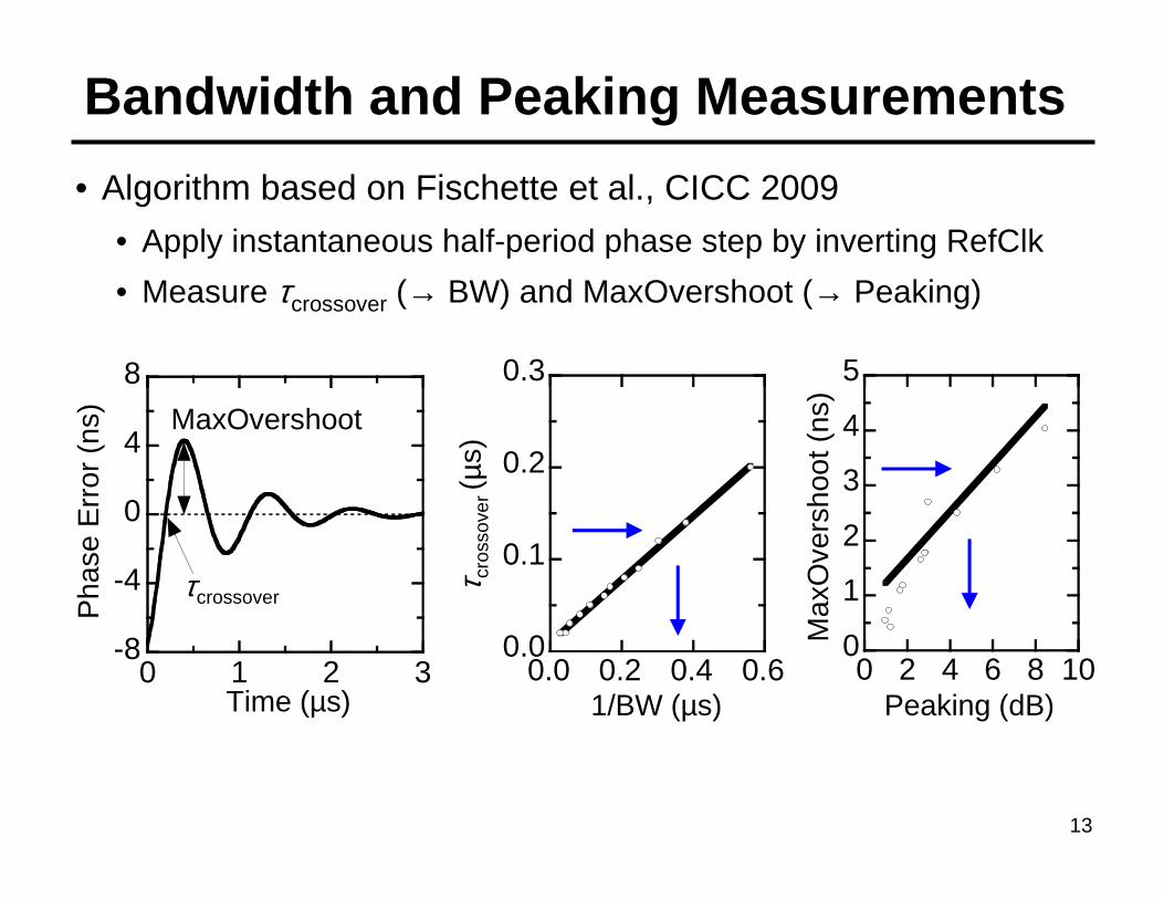
Bandwidth and Peaking Measurements
• Algorithm based on Fischette et al., CICC 2009
• Apply instantaneous half-period phase step by inverting RefClk
• Measure τcrossover (→ BW) and MaxOvershoot (→ Peaking)
Time (µs)
Pha
se E
rror
(ns
) MaxOvershoot
τcrossover
1/BW (µs)
τ cro
ssov
er (µ
s)
Peaking (dB)
Max
Ove
rsho
ot (
ns)
0
1
2
3
4
5
0 2 4 6 8 100.0
0.1
0.2
0.3
0.0 0.2 0.4 0.6
14
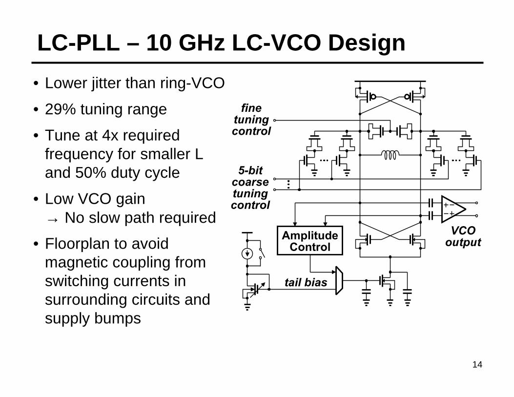
LC-PLL – 10 GHz LC-VCO Design
• Lower jitter than ring-VCO
• 29% tuning range
• Tune at 4x required frequency for smaller Land 50% duty cycle
• Low VCO gain → No slow path required
• Floorplan to avoid magnetic coupling from switching currents in surrounding circuits and supply bumps
5-bitcoarsetuningcontrol
finetuningcontrol
AmplitudeControl
VCO output
tail bias
15
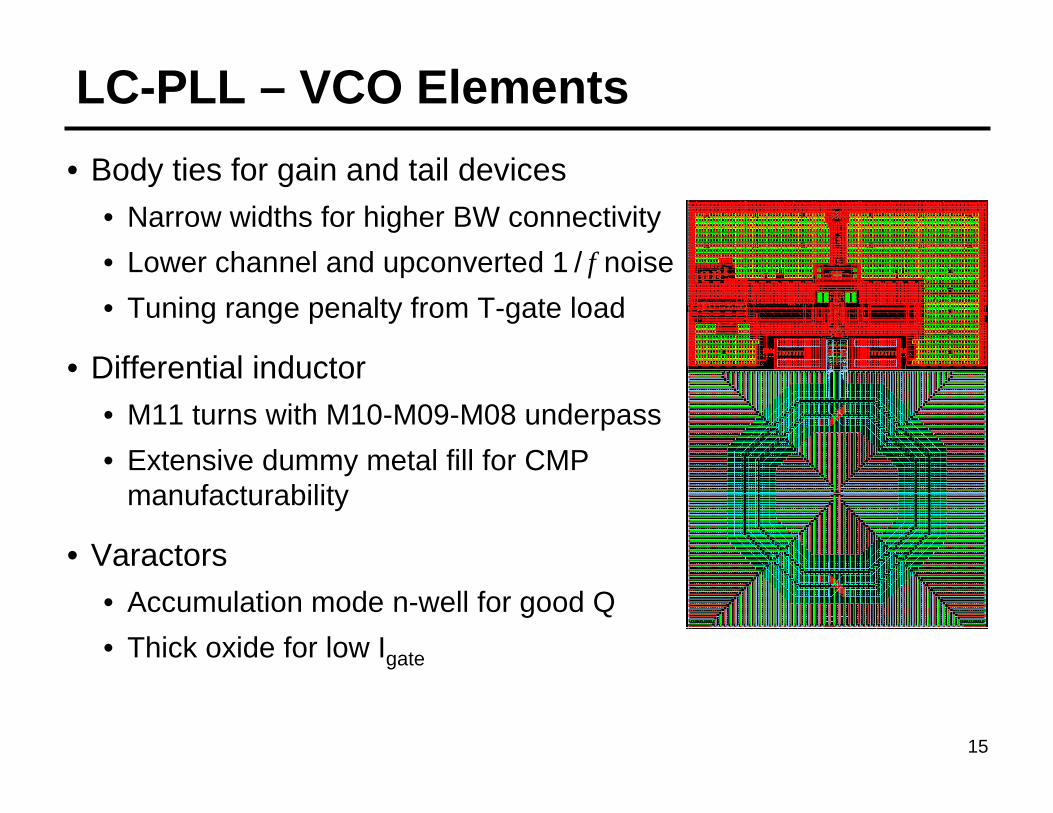
LC-PLL – VCO Elements
• Body ties for gain and tail devices
• Narrow widths for higher BW connectivity
• Lower channel and upconverted 1 / f noise
• Tuning range penalty from T-gate load
• Differential inductor• M11 turns with M10-M09-M08 underpass
• Extensive dummy metal fill for CMP manufacturability
• Varactors
• Accumulation mode n-well for good Q
• Thick oxide for low Igate
16
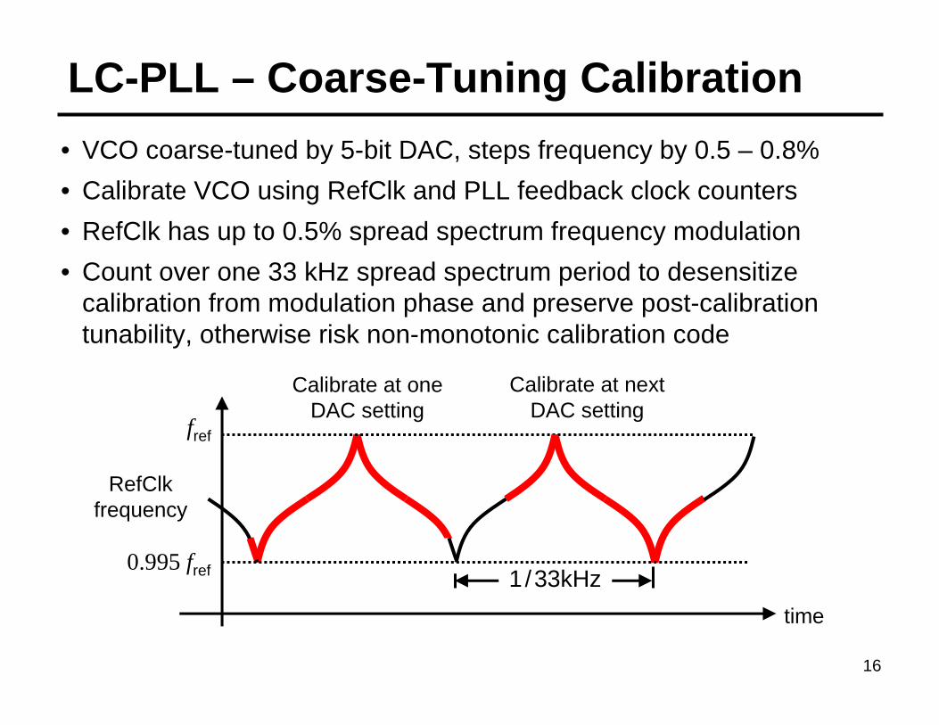
LC-PLL – Coarse-Tuning Calibration
• VCO coarse-tuned by 5-bit DAC, steps frequency by 0.5 – 0.8%
• Calibrate VCO using RefClk and PLL feedback clock counters
• RefClk has up to 0.5% spread spectrum frequency modulation
• Count over one 33 kHz spread spectrum period to desensitize calibration from modulation phase and preserve post-calibration tunability, otherwise risk non-monotonic calibration code
time
0.995 fref 1/33kHz
RefClk frequency
fref
Calibrate at one DAC setting
Calibrate at next DAC setting
17
Outline
• Introduction
• Architecture and Circuits• Ring-based PLL• LC-based PLL
•• Silicon ResultsSilicon Results
• Conclusion
18
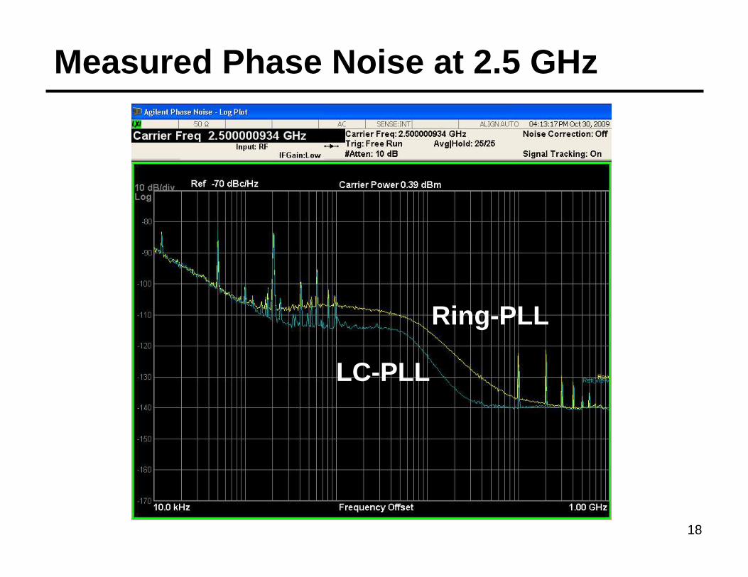
Measured Phase Noise at 2.5 GHz
Ring-PLL
LC-PLL
19
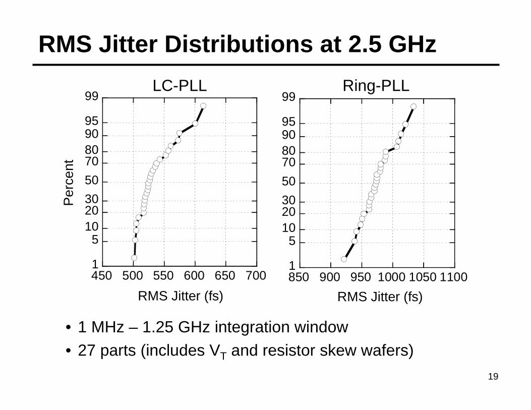
RMS Jitter Distributions at 2.5 GHz
RMS Jitter (fs)
Per
cent
Ring-PLL
• 1 MHz – 1.25 GHz integration window
• 27 parts (includes VT and resistor skew wafers)
LC-PLL
RMS Jitter (fs)
450 500 550 600 650 7001
5102030
50
70809095
99
850 900 950 1000 1050 11001
5102030
50
70809095
99
20
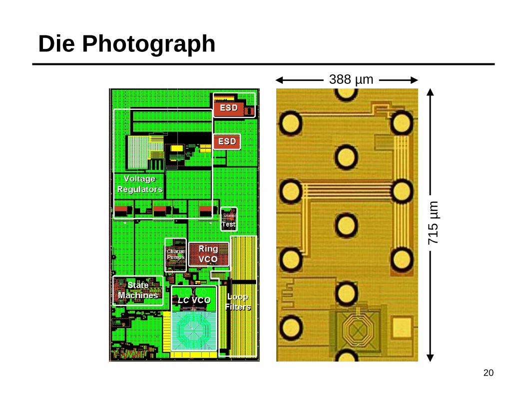
Die Photograph 388 µm
715
µm
21
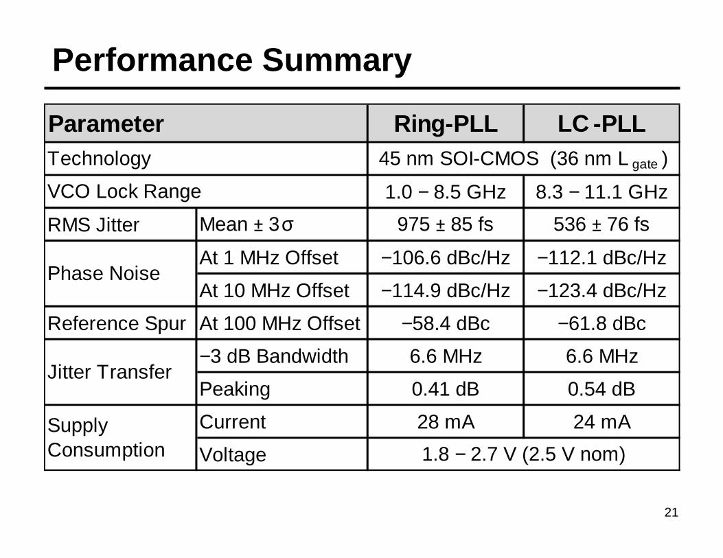
Performance Summary
Ring-PLL LC -PLL
1.0 − 8.5 GHz 8.3 − 11.1 GHz
RMS Jitter Mean 3 σ 975 85 fs 536 76 fs
At 1 MHz Offset −106.6 dBc/Hz −112.1 dBc/Hz
At 10 MHz Offset −114.9 dBc/Hz −123.4 dBc/Hz
Reference Spur At 100 MHz Offset −58.4 dBc −61.8 dBc
−3 dB Bandwidth 6.6 MHz 6.6 MHz
Peaking 0.41 dB 0.54 dB
Current 28 mA 24 mA
Voltage
Parameter
VCO Lock Range
SupplyConsumption
Jitter Transfer
Phase Noise
45 nm SOI-CMOS (36 nm L gate )
1.8 − 2.7 V (2.5 V nom)
Technology
22
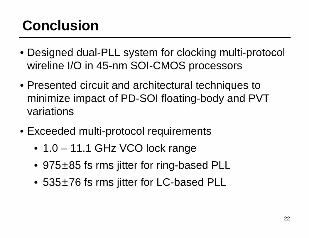
Conclusion
• Designed dual-PLL system for clocking multi-protocol wireline I/O in 45-nm SOI-CMOS processors
• Presented circuit and architectural techniques to minimize impact of PD-SOI floating-body and PVT variations
• Exceeded multi-protocol requirements
• 1.0 – 11.1 GHz VCO lock range
• 975±85 fs rms jitter for ring-based PLL
• 535±76 fs rms jitter for LC-based PLL
23
Acknowledgments
AMD• Larry Bair• John Faricelli• Kurt Ireland• Chad Lackey• Jim Pattison• Norma Rodriguez• Keertika Singh• Sam Sim
GlobalFoundries• Jung-Suk Goo• Tilo Mantei• René Nagel• Lynne Okada• Christoph Schwan• Rasit Topaloglu• Thomas Werner• Jianhong Zhu
Thank you for your attention!