Design of a Tunable Active Low Pass Filter by
CMOS OTA and a Comparative Study with
NMOS OTA with Different Current Mirror Loads
T. K. Das and S. Chakrabarti Future Institute of Engg. and Management/ECE Department, Kolkata, India
Email: [email protected], [email protected]
Abstract—The operational amplifiers (OPAMP) are basic
building blocks in implementing a variety of analog circuits
such as amplifiers, filters, integrators, differentiators,
summers, oscillators etc. OPAMPs work well for low-
frequency applications, such as audio and video systems.
For higher frequencies, however, OPAMP designs become
difficult due to their frequency limit. At those high
frequencies, operational transconductance amplifiers (OTAs)
are deemed to be promising to replace OPAMPS as the
building blocks. This paper illustrates an application of
OTA as an active low pass filter. The primary building
block of an OTA is the current mirror. In this paper
different current mirrors are used to design the LPF & the
corresponding frequency and phase responses are
comparatively studied. Also a comparative study of CMOS
OTA & NMOS OTA is also illustrated in this paper. Finally,
the applications of OTA based LPF are also studied. Index Terms—complementary MOSFET, current mirror,
low pass filter, operational transconductance amplifier
I. INTRODUCTION
An active low pass filter is an analog circuit that is
widely used in communication systems and signal
processing to pass a range of frequencies & reject the
higher frequency [1]. It can be easily designed by a
conventional operational amplifier. But CMOS
operational transconductance amplifier can be used to
design a LPF resulting reduced power dissipation &
fabrication cost [1]-[5]. Some earlier works are enlisted in
the references [6]-[11] where CMOS OTA is used. But in
this paper we have started our work with NMOS OTA
with different current mirror loads. Then we have
designed the LPF by CMOS OTA with different current
mirror loads. Finally a comparative study was
investigated to draw the conclusion that CMOS OTA is
much more superior to NMOS OTA in designing analog
circuits.
II. THEORY AND PRINCIPLES
A. Basic Concept of OTA
An OTA is a voltage controlled current source, more
specifically the term “operational” comes from the fact
Manuscript received January 24, 2014; revised October 20, 2014.
that it takes the difference of two voltages as the input for
the output current conversion. The ideal transfer
characteristic is therefore,
( )out m in inI g V V (1)
where Vin+=Input voltage applied at the non-inverting
input terminal of the OTA, Vin-=Input voltage applied at
the inverting input terminal of the OTA and
gm=Transconductance of the OTA.
An ideal OTA has two voltage inputs with infinite
impedance (i.e. there is no input current). The common
mode input range is also infinite, while the differential
signal between these two inputs is used to control an ideal
current source (i.e. the output current does not depend on
the output voltage) that functions as an output. The
proportionality factor between output current and input
differential voltage is called transconductance. Fig. 1, Fig.
2 and Fig. 3 show the macro model, ideal model and
small signal equivalent model of OTA respectively.
Figure 1. Macro model of OTA.
Figure 2. Ideal model of OTA.
Figure 3. Small signal equivalent model of OTA.
International Journal of Electronics and Electrical Engineering Vol. 3, No. 5, October 2015
©2015 Engineering and Technology Publishing 37710.12720/ijeee.3.5.377-384doi:
The amplifier’s output voltage is the product of its
output current and its load resistance:
OUTout loadV I R (2)
The voltage gain is then the output voltage divided by
the differential input voltage:
outm load m
in in
VG R g
V V
(3)
B. Current Mirror Fundamentals
An OTA is basically a differential amplifier with
active current mirror load to accomplish high gain. As the
name itself suggests a current mirror is used to generate a
replica (if necessary it may be attenuated or amplified) of
a given reference current. If we look at the electric
function of the circuit, a current mirror is a current
controlled current source (CCCS).
A current mirror is basically nothing more than a
current amplifier. The ideal characteristics of a current
amplifier are:
Output current linearly related to the input current,
Iout=Ai.Iref
Input resistance is zero
Output resistance is infinity
In addition, we have the characteristic Vmin which
applies not only to the output but also the input. Vmin (in)
is the range of input voltage over which the input
resistance is not small and Vmin (out) is the range of the
output voltage over which the output resistance is not
large. Fig. 4, Fig. 5 and Fig. 6 show the block diagram,
transfer characteristics and output characteristics of a
current mirror respectively.
Figure 4. Block diagram of current mirror.
Figure 5. Transfer characteristics of current mirror.
Figure 6. Output characteristics of current mirror.
Therefore, we will focus on Rout, Rin, Vmin (out),
Vmin (in), and Ai to characterize the current mirror. We
can design a number of circuits which can accomplish the
current mirror function. The ones mostly used are:
1. Simple Current Mirror
2. Wilson Current Mirror
3. Cascode Current Mirror
Simple current mirror (Widlar)
Fig. 7 below shows the schematic circuit diagram of a
simple current mirror.
Figure 7. Schematic circuit diagram of simple current mirror.
We assume that VDS2>VGS –VT2 then,
2
2 21 2 2
2 1 1 1 1
1 '
1 '
out GS T DS
ref GS T DS
i V V VLW K
i L W V V V K
(4)
If the transistors are matched, then K1’=K2
’ and
VT1=VT2 to give:
21 2
2 1 1
1
1
out DS
ref DS
i VLW
i L W V
(5)
If VDS1=VDS2 then, we have
1 2
2 1
o
ref
i LW
i L W
(6)
Therefore the sources of errors are:
1) VDS1 and VDS2 are not equal.
2) M1 and M2 are not matched.
3) Channel length modulation (λ) and
4) Threshold offset.
Fig. 8 shows the small signal equivalent model of a
simple current mirror.
Figure 8. Small signal equivalent model of simple current mirror.
Finally,
2 1
1 2 1
/
1 ( ) /
out m m
ref gs gs m
i g g
i S C C g
(7)
Wilson current mirror
Fig. 9 below shows the schematic circuit diagram of a
Wilson current mirror.
International Journal of Electronics and Electrical Engineering Vol. 3, No. 5, October 2015
©2015 Engineering and Technology Publishing 378

Figure 9. Schematic circuit diagram of Wilson current mirror.
here, VGS1=VGS2, so ID1 is almost equal to ID2. Then,
21
1
2
1
1
out DS
ref DS
W
i VL
Wi V
L
(8)
Since, VDS1=VDS2+VGS3
21
2 3
2
1
1 ( )
out DS
ref DS GS
W
i VL
Wi V V
L
(9)
The output voltage swing is limited to
2,min ,3 2GSout DSsat Th DSsatV I V V V (10)
It uses negative series feedback (M3) to achieve higher
output resistance. Fig. 10 shows the small signal
equivalent model of a Wilson current mirror.
Figure 10. Small signal equivalent model of Wilson current mirror.
Cascode current mirror
Fig. 11 below shows the schematic circuit diagram of a
cascode current mirror.
Figure 11. Schematic circuit diagram of cascode current mirror.
An alternative way to increase the output resistance is
to use the cascade configuration. The output stage
consists of two transistors M2, M3 in the cascade
arrangement. They are biases result from two other
transistors M1 M4 which are diode connected. Again, as
for the previously started current mirror the VGS voltage
of M1 and M2 are set equal. Therefore a replica of
current in M1 is generated by M2. The output resistance
increases because of the cascode arrangement. Here,
21 3 4DSDS GS GSV V V V (11)
If VGS3=VGS4 then, VDS1=VDS2. Finally,
International Journal of Electronics and Electrical Engineering Vol. 3, No. 5, October 2015
©2015 Engineering and Technology Publishing 379
21 1
1
2 2
1
1
out DS
ref DS
W W
i VL L
W Wi V
L L
(12)
Fig. 12 below shows the small signal equivalent model
of a cascode current mirror.
Figure 12. Small signal equivalent model of cascode current mirror.
The output swing is limited to
1,min 4 3 ,3GSout GS GS DSsatV V V V V (13)
2,min ,3 2GSout DSsat TH DSsatV V V V V (14)
Hence, the output resistance is increased without
feedback.
C. NMOS OTA Design with Current Mirror Loads
Fig. 13, Fig. 14 and Fig. 15 show the circuit diagram of
NMOS OTA with simple, Wilson and cascode current
mirror loads respectively.
Figure 13. Circuit diagram of NMOS OTA with simple current mirrorload.
Figure 14. Circuit diagram of NMOS OTA with Wilson current mirror load.
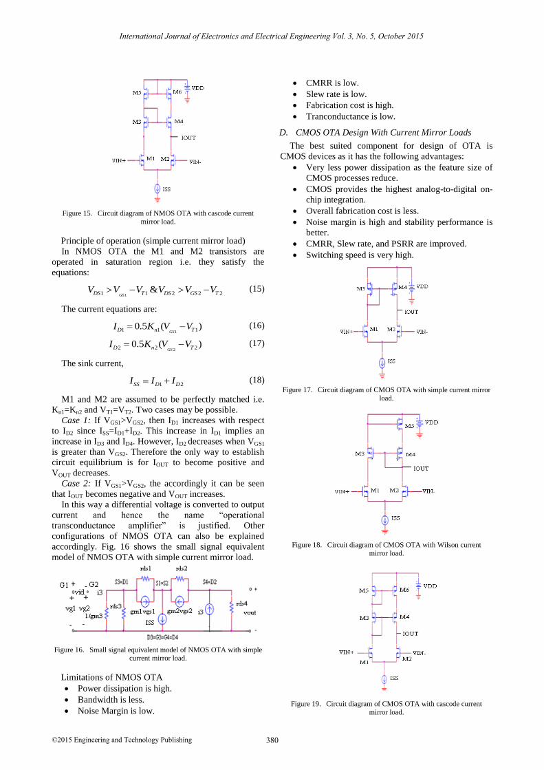
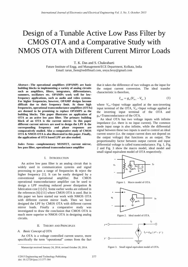
Figure 15. Circuit diagram of NMOS OTA with cascode current mirror load.
Principle of operation (simple current mirror load)
In NMOS OTA the M1 and M2 transistors are
operated in saturation region i.e. they satisfy the
equations:
11 1 2 2 2&GSDS T DS GS TV V V V V V (15)
The current equations are:
11 1 10.5 ( )GSD n TI K V V (16)
22 2 20.5 ( )GSD n TI K V V (17)
The sink current,
1 2SS D DI I I (18)
M1 and M2 are assumed to be perfectly matched i.e.
Kn1=Kn2 and VT1=VT2. Two cases may be possible.
Case 1: If VGS1>VGS2, then ID1 increases with respect
to ID2 since ISS=ID1+ID2. This increase in ID1 implies an
increase in ID3 and ID4. However, ID2 decreases when VGS1
is greater than VGS2. Therefore the only way to establish
circuit equilibrium is for IOUT to become positive and
VOUT decreases.
Case 2: If VGS1>VGS2, the accordingly it can be seen
that IOUT becomes negative and VOUT increases.
In this way a differential voltage is converted to output
current and hence the name “operational
transconductance amplifier” is justified. Other
configurations of NMOS OTA can also be explained
accordingly. Fig. 16 shows the small signal equivalent
model of NMOS OTA with simple current mirror load.
Figure 16. Small signal equivalent model of NMOS OTA with simple current mirror load.
Limitations of NMOS OTA
Power dissipation is high.
Bandwidth is less.
Noise Margin is low.
CMRR is low.
Slew rate is low.
Fabrication cost is high.
Tranconductance is low.
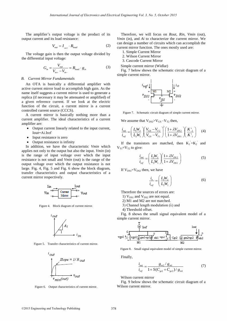
D. CMOS OTA Design With Current Mirror Loads
The best suited component for design of OTA is
CMOS devices as it has the following advantages:
Very less power dissipation as the feature size of
CMOS processes reduce.
CMOS provides the highest analog-to-digital on-
chip integration.
Overall fabrication cost is less.
Noise margin is high and stability performance is
better.
CMRR, Slew rate, and PSRR are improved.
Switching speed is very high.
Figure 17. Circuit diagram of CMOS OTA with simple current mirror load.
Figure 18. Circuit diagram of CMOS OTA with Wilson current mirror load.
Figure 19. Circuit diagram of CMOS OTA with cascode current mirror load.
International Journal of Electronics and Electrical Engineering Vol. 3, No. 5, October 2015
©2015 Engineering and Technology Publishing 380
In CMOS OTA the differential amplifier part is exactly
same as NMOS OTA, consisting of two NMOS
enhancement mode transistors. But the current mirror part
(I-V conversion) is made of PMOS enhancement mode
transistors as shown in the following figures. Fig. 17, Fig.
18 and Fig. 19 show the circuit diagram of CMOS OTA
with simple, Wilson and cascode current mirror loads
respectively.
Fig. 20 below shows the small signal equivalent model
of CMOS OTA with simple current mirror load.
Figure 20. Small signal equivalent model of CMOS OTA with simple current mirror load.
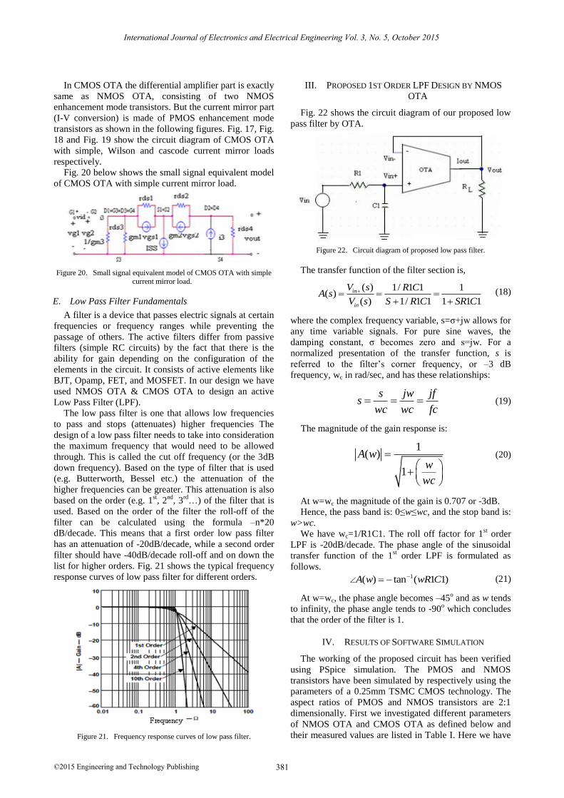
E. Low Pass Filter Fundamentals
A filter is a device that passes electric signals at certain
frequencies or frequency ranges while preventing the
passage of others. The active filters differ from passive
filters (simple RC circuits) by the fact that there is the
ability for gain depending on the configuration of the
elements in the circuit. It consists of active elements like
BJT, Opamp, FET, and MOSFET. In our design we have
used NMOS OTA & CMOS OTA to design an active
Low Pass Filter (LPF).
The low pass filter is one that allows low frequencies
to pass and stops (attenuates) higher frequencies The
design of a low pass filter needs to take into consideration
the maximum frequency that would need to be allowed
through. This is called the cut off frequency (or the 3dB
down frequency). Based on the type of filter that is used
(e.g. Butterworth, Bessel etc.) the attenuation of the
higher frequencies can be greater. This attenuation is also
based on the order (e.g. 1st, 2
nd, 3
rd…) of the filter that is
used. Based on the order of the filter the roll-off of the
filter can be calculated using the formula –n*20
dB/decade. This means that a first order low pass filter
has an attenuation of -20dB/decade, while a second order
filter should have -40dB/decade roll-off and on down the
list for higher orders. Fig. 21 shows the typical frequency
response curves of low pass filter for different orders.
Figure 21. Frequency response curves of low pass filter.
III. PROPOSED 1ST ORDER LPF DESIGN BY NMOS
OTA
Fig. 22 shows the circuit diagram of our proposed low
pass filter by OTA.
Figure 22. Circuit diagram of proposed low pass filter.
The transfer function of the filter section is,
( ) 1/ 1 1 1( )
( ) 1/ 1 1 1 1 1
in
in
V s R CA s
V s S R C SR C
(18)
where the complex frequency variable, s=σ+jw allows for
any time variable signals. For pure sine waves, the
damping constant, σ becomes zero and s=jw. For a
normalized presentation of the transfer function, s is
referred to the filter’s corner frequency, or –3 dB
frequency, wc in rad/sec, and has these relationships:
s jw jfs
wc wc fc (19)
The magnitude of the gain response is:
1( )
1
A ww
wc
(20)
At w=wc the magnitude of the gain is 0.707 or -3dB.
Hence, the pass band is: 0≤w≤wc, and the stop band is:
w>wc.
We have wc=1/R1C1. The roll off factor for 1st order
LPF is -20dB/decade. The phase angle of the sinusoidal
transfer function of the 1st order LPF is formulated as
follows. 1( ) tan ( 1 1)A w wR C
(21)
At w=wc, the phase angle becomes –45o and as w tends
to infinity, the phase angle tends to -90o which concludes
that the order of the filter is 1.
IV. RESULTS OF SOFTWARE SIMULATION
The working of the proposed circuit has been verified
using PSpice simulation. The PMOS and NMOS
transistors have been simulated by respectively using the
parameters of a 0.25mm TSMC CMOS technology. The
aspect ratios of PMOS and NMOS transistors are 2:1
dimensionally. First we investigated different parameters
of NMOS OTA and CMOS OTA as defined below and
their measured values are listed in Table I. Here we have
International Journal of Electronics and Electrical Engineering Vol. 3, No. 5, October 2015
©2015 Engineering and Technology Publishing 381
set, Vdd=5V, Cload=1pF for all the circuits and tuned ISS
to get positive output voltage. The calculations are done
according to the following definitions of the parameters.
1) Output Offset Voltage (Voo) is the output voltage,
Vout with Vin+=Vin-=0V
2) ( ) 20logAd
CMRR dBAcm
(22)
where, Ad=Differential Voltage gain and Acm=Common
mode voltage gain.
3) / ( 0 )( ) 20log
/ ( 0 )
O
O
V Vid Vdd VPSRR dB
V Vdd Vid V
(23)
4) ( ) /outVSiew Rate SR V s
V
(24)
For Vin+=u(t), unit step signal with Vin-=0V.
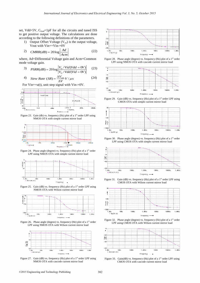
Figure 23. Gain (db) vs. frequency (Hz) plot of a 1st order LPF using NMOS OTA with simple current mirror load
Figure 24. Phase angle (degree) vs. frequency (Hz) plot of a 1st order
LPF using NMOS OTA with simple current mirror load
Figure 25. Gain (dB) vs. frequency (Hz) plot of a 1st order LPF using NMOS OTA with Wilson current mirror load
Figure 26. Phase angle (degree) vs. frequency (Hz) plot of a 1st order LPF using NMOS OTA with Wilson current mirror load
Figure 27. Gain (dB) vs. frequency (Hz) plot of a 1st order LPF using NMOS OTA with cascode current mirror load
Figure 28. Phase angle (degree) vs. frequency (Hz) plot of a 1st order LPF using NMOS OTA with cascode current mirror load
Figure 29. Gain (dB) vs. frequency (Hz) plot of a 1st order LPF using CMOS OTA with simple current mirror load
Figure 30. Phase angle (degree) vs. frequency (Hz) plot of a 1st order
LPF using CMOS OTA with simple current mirror load
Figure 31. Gain (dB) vs. frequency (Hz) plot of a 1st order LPF using CMOS OTA with Wilson current mirror load
Figure 32. Phase angle (degree) vs. frequency (Hz) plot of a 1st order LPF using CMOS OTA with Wilson current mirror load
Figure 33. Gain(dB) vs. frequency (Hz) plot of a 1st order LPF using CMOS OTA with cascode current mirror load
International Journal of Electronics and Electrical Engineering Vol. 3, No. 5, October 2015
©2015 Engineering and Technology Publishing 382
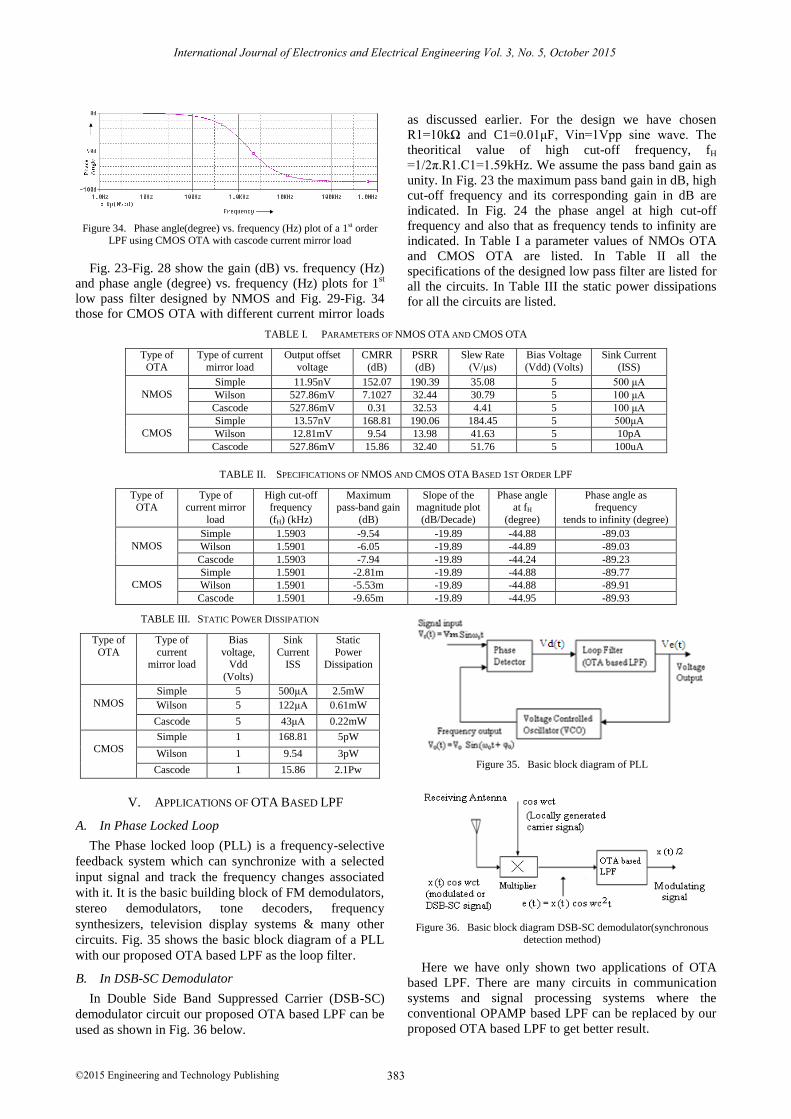
Figure 34. Phase angle(degree) vs. frequency (Hz) plot of a 1st order LPF using CMOS OTA with cascode current mirror load
Fig. 23-Fig. 28 show the gain (dB) vs. frequency (Hz)
and phase angle (degree) vs. frequency (Hz) plots for 1st
low pass filter designed by NMOS and Fig. 29-Fig. 34
those for CMOS OTA with different current mirror loads
as discussed earlier. For the design we have chosen
R1=10kΩ and C1=0.01μF, Vin=1Vpp sine wave. The
theoritical value of high cut-off frequency, fH
=1/2π.R1.C1=1.59kHz. We assume the pass band gain as
unity. In Fig. 23 the maximum pass band gain in dB, high
cut-off frequency and its corresponding gain in dB are
indicated. In Fig. 24 the phase angel at high cut-off
frequency and also that as frequency tends to infinity are
indicated. In Table I a parameter values of NMOs OTA
and CMOS OTA are listed. In Table II all the
specifications of the designed low pass filter are listed for
all the circuits. In Table III the static power dissipations
for all the circuits are listed.
TABLE I. PARAMETERS OF NMOS OTA AND CMOS OTA
Type of
OTA
Type of current
mirror load
Output offset
voltage
CMRR
(dB)
PSRR
(dB)
Slew Rate
(V/μs)
Bias Voltage
(Vdd) (Volts)
Sink Current
(ISS)
NMOS
Simple 11.95nV 152.07 190.39 35.08 5 500 μA
Wilson 527.86mV 7.1027 32.44 30.79 5 100 μA
Cascode 527.86mV 0.31 32.53 4.41 5 100 μA
CMOS
Simple 13.57nV 168.81 190.06 184.45 5 500μA
Wilson 12.81mV 9.54 13.98 41.63 5 10pA
Cascode 527.86mV 15.86 32.40 51.76 5 100uA
TABLE II. SPECIFICATIONS OF NMOS AND CMOS OTA BASED 1ST ORDER LPF
Type of OTA
Type of current mirror
load
High cut-off frequency
(fH) (kHz)
Maximum pass-band gain
(dB)
Slope of the magnitude plot
(dB/Decade)
Phase angle at fH
(degree)
Phase angle as frequency
tends to infinity (degree)
NMOS
Simple 1.5903 -9.54 -19.89 -44.88 -89.03
Wilson 1.5901 -6.05 -19.89 -44.89 -89.03
Cascode 1.5903 -7.94 -19.89 -44.24 -89.23
CMOS
Simple 1.5901 -2.81m -19.89 -44.88 -89.77
Wilson 1.5901 -5.53m -19.89 -44.88 -89.91
Cascode 1.5901 -9.65m -19.89 -44.95 -89.93
TABLE III. STATIC POWER DISSIPATION
Type of
OTA
Type of
current mirror load
Bias
voltage, Vdd
(Volts)
Sink
Current ISS
Static
Power Dissipation
NMOS
Simple 5 500μA 2.5mW
Wilson 5 122μA 0.61mW
Cascode 5 43μA 0.22mW
CMOS
Simple 1 168.81 5pW
Wilson 1 9.54 3pW
Cascode 1 15.86 2.1Pw
V. APPLICATIONS OF OTA BASED LPF
A. In Phase Locked Loop
The Phase locked loop (PLL) is a frequency-selective
feedback system which can synchronize with a selected
input signal and track the frequency changes associated
with it. It is the basic building block of FM demodulators,
stereo demodulators, tone decoders, frequency
synthesizers, television display systems & many other
circuits. Fig. 35 shows the basic block diagram of a PLL
with our proposed OTA based LPF as the loop filter.
B. In DSB-SC Demodulator
In Double Side Band Suppressed Carrier (DSB-SC)
demodulator circuit our proposed OTA based LPF can be
used as shown in Fig. 36 below.
Figure 35. Basic block diagram of PLL
Figure 36. Basic block diagram DSB-SC demodulator(synchronous detection method)
Here we have only shown two applications of OTA
based LPF. There are many circuits in communication
systems and signal processing systems where the
conventional OPAMP based LPF can be replaced by our
proposed OTA based LPF to get better result.
International Journal of Electronics and Electrical Engineering Vol. 3, No. 5, October 2015
©2015 Engineering and Technology Publishing 383

VI. CONCLUSIONS
From Table III we can conclude that the CMOS based
OTA reduces the static power dissipations drastically &
also the pass band gain is nearer to 0dB i.e. unity gain
which is our objective. It may be further noted that the
bias voltage for CMOS OTA is reduced greatly. We call
our proposed OTA based LPF as tunable because by
adjusting the values of power supply and sink current we
can get different pass band gain less than unity. Again,
the high cut-off frequency can be adjusted by changing
simply the values of resistor, R and capacitor, C of the
input RC section. The other advantages of our design
over conventional OPAMP based LPF are (1) a single
power supply is required, (2) CMRR, PSRR, slew rate are
better. (3) noise margin is high, (4) design is very simple,
(5) fabrication cost is reduced greatly.
VII. FUTURE SCOPE
Here we have designed a 1st order LPF with different
current mirror loads and a comparative study was
analyzed. The OTA can be used to design higher order
filters to get more ideal frequency response by simply
including more RC sections at the non-inverting terminal
of the OTA. Also the higher pass band can be obtained by
changing the value of R and C. Again, pass band gain can
be increased by adding a feedback resistor voltage divider
section at the inverting input terminal of the OTA. The
OTA can be designed practically in IC fabrication lab and
the practical applications of OTA based LPF can be
studied. In our design for the CMOS OTA we have used
NMOS transistors to design the differential amplifier with
PMOS transistors for the current mirror section. These
transistors can be interchanged & the change at the output
can be studied.
REFERENCES
[1] C.-L. Hsu, M.-H. Ho, Y.-K. Wu, and T.-H. Chen, “Design of low-frequency low-pass filters for biomedical applications,” in Proc.
IEEE Asia Pacific Conference on Circuits and Systems, Dec. 2006,
pp. 690-695. [2] E. R. Villegas, A. J. Casson, and P. Corbishley, “A subhertz
nanopower low-pass filter,” IEEE Transactions on Circuits and
Systems II, vol. 58, no. 6, pp. 351-355, Jun. 2011. [3] H. Liu, X. Peng, and W. Wu, “Design of a Gm-C low pass filter
with low cutoff frequency,” in Proc. Asia Pacific Conference on
Postgraduate Research in Microelectronics and Electronics, Jan. 2009, pp. 125-128.
[4] P. K. Mahapatra, M. Singh, and N. Kumar, “Realization of active filters using operational transconductance amplifier (OTA),”
Journal of the Instrument Society of India, vol. 35, no. 1, pp 1-9,
2009. [5] R. L. Geiger and E. Sánchez-Sinencio, “Active filter design using
operational transconductance amplifiers: A tutorial,” IEEE
Circuits and Devices Magazine, vol. 1, pp. 20-32, Mar. 1985. [6] H. S. Malvar, “Electronically controlled active filters with
operational transconductance amplifier,” IEEE Transactions on
Circuits and Systems, vol. CAS 29, pp. 333-336, May 1982. [7] F. Rezzi, A. Bashirotto, and R. Castello, “A 3V 12-55MHz
BiCMOS pseudo-differential continuous-time filter,” IEEE
Transactions on Circuits and System I, vol. 42, pp. 896-903, Nov. 1995.
[8] A. Timar and M. Rencz, “Design issues of a low frequency low-
pass filter for medical applications using CMOS technology,” in Proc. IEEE Design and Diagnostics of Electronic Circuits and
Systems, Apr. 2007, pp. 1-4.
[9] S. Solis-Bustos, J. S. Martinez, F. Maloberti, and E. Sanchez-Sinencio, “A 60-dB dynamic-range CMOS sixth-order 2.4-Hz
low-pass filter for medical applications,” IEEE Transactions on
Circuits and Systems, vol. 47, no. 12, pp. 1391-1398, Dec. 2000. [10] T.-Y. Lo and C. C. Hung, “A 1-V Gm-C low-pass filter for uwb
wireless application,” in Proc. IEEE Asian Solid-State Circuits
Conference, Nov. 2008, pp. 277-280. [11] W. R. Grise. Application of the operational transconductance
amplifier to voltage controlled amplifiers and active filters.
TECHNOLOGY INTREFACE: The Electronic Journal for Engg. Technology [Online]. Available: http://et.nmsu.edu/~etti
Tarun Kumar Das was born in Kolkata, India in 1979. He received the B.Tech. degree in
Electronics & Communication Engineering
from Murshidabad College of Engg. & Technology under West Bengal University of
Technology, India in 2003, M.Tech. degree in
software engineering from West Bengal University of Technology, India in 2008.
Currently he is an assistant professor in Electronics & Communication Engineering
Department at Future Institute of Engineering & Management under
West Bengal University of Technology. His research interest includes microelectronics & VLSI technology, control system and signal
processing.
Sreya Chakrabarti was born in Barakar, India
in 1983. She received the B.Tech. degree in
Electronics & Communication Engineering from Dr.B.C. Roy Engineering College under
Burdwan University, India in 2004, M.Tech.
degree in computer science & engineering from West Bengal University of Technology,
India in 2007. Currently she is an assistant
professor in Electronics & Communication Engineering Department at Future Institute of
Engineering & Management under West Bengal University of
Technology. His research interest includes microelectronics & VLSI technology, embedded systems and satellite communication.
International Journal of Electronics and Electrical Engineering Vol. 3, No. 5, October 2015
©2015 Engineering and Technology Publishing 384


