Driving the future of HEV/EV with high-voltage solutions
Nagarajan SridharManager, Strategy and Business Development - Automotive and Isolated Driver Solutions, High Voltage PowerTexas Instruments

Driving the future of HEV/EV with high-voltage solutions 2 July 2017
Introduction
The foundation for HEV/EV architectures is high
voltage. These vehicles are based on high-voltage
battery systems, such as +400V for EVs and 48V
for HEVs.
The basis for energy-efficiency improvements
through high voltage will occur through the
advancement of switch-mode power supplies
(SMPS) enabled by power electronics.
In addition to energy-efficiency improvements, the
incorporation of high voltage makes system wiring
less complex and lighter. This in effect lowers the
vehicle’s overall weight, in addition to overcoming
other disadvantages in a 12V system [2]. High
voltage also contributes to an overall vehicle
efficiency improvement in terms of miles per gallon
(MPG) for fuel-injection vehicles and miles per
charge for HEVs and EVs.
The incorporation of advanced high-voltage devices
such as wideband-gap semiconductors makes
it possible for HEVs/EVs to withstand extreme
high-temperature conditions and exhibit improved
thermal-management efficiency.
In this white paper, I will discuss the value of
high voltage and SMPS in two subsystems – an
on-board charger (OBC) and a traction inverter
– with an emphasis on the advanced power
electronics required to handle them and the overall
trend toward wideband-gap semiconductors.
The SMPS concept
SMPS is based on the operation of the on and off
states of semiconductor power switches. SMPS
implies no power loss at either state because there
is zero current during the off state and zero voltage
during the on state. In theory, this is 100 percent
efficiency.
With pulse-width modulation (PWM), these switches
operate under high switching frequencies, making
the power-converter systems less bulky and smaller.
There are three types of power conditioners found in
powertrain electrification systems: AC/DC (rectifier),
DC/DC (converter) and DC/AC (inverter).
SMPS in powertrain electrification
SMPS conditioners are realized in these power train
sub-systems in HEVs/EVs:
• AC/DC
° Regenerative braking
° OBC
• DC/DC dual-battery system
° Battery management for lithium-ion (Li-Ion)
batteries
° 48V to 12V bidirectional power supplies
° 400V batteries (EVs only)
° Bidirectional 400V to 12V power supplies
• DC/AC
° Traction motors
° Auxiliary inverters
Energy efficiency has become a key global focus because of its contribution toward reduced carbon-dioxide emissions. One significant area of contribution is the electrification of vehicular technology.
Automotive manufacturers are building and increasing electrification in vehicle powertrains in the form of hybrid electric vehicles and electric vehicles (HEVs/EVs). HEV/EV sales are expected to represent between 5 and 20 percent of all cars sold by 2025 [1].
Driving the future of HEV/EV with high-voltage solutions 3 July 2017
On-board charging
An OBC charges the batteries in an HEV/EV by
connecting the vehicle to the grid, which is the
electric power source. The grid is AC and the battery
is DC, so the charger is an AC/DC system. Because
the charger is built into the vehicle and therefore
called “on-board,” it must be as small and light
as possible.
One key trend currently under development is
power (from the grid to charge the battery in the
car) greater than 3.3kW (which has been the
traditional power level) to enable fast charging. Fast
charging is vital in order for HEVs/EVs to compete
against gasoline-powered vehicles, which drivers
can fill up with gas in just a few minutes. However,
with increasing switching frequency and adoption
of wideband-gap power switches, the size and
dimensions can be prevented from increasing
proportionately larger.
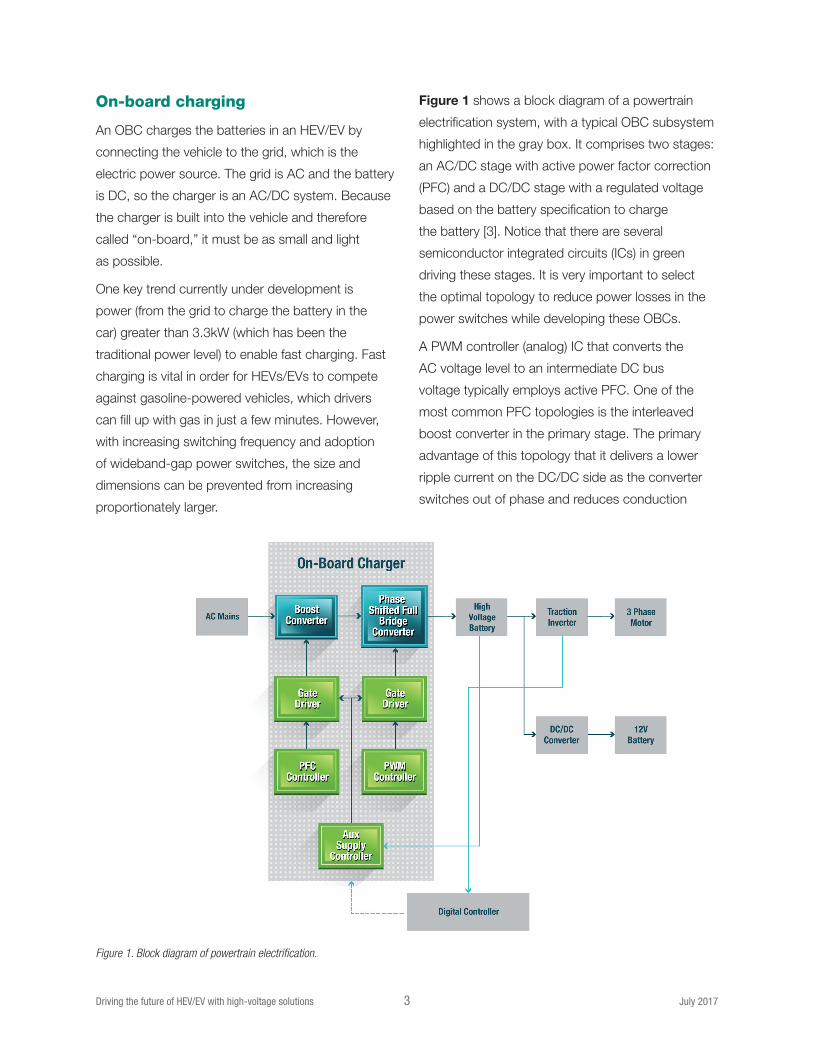
Figure 1 shows a block diagram of a powertrain
electrification system, with a typical OBC subsystem
highlighted in the gray box. It comprises two stages:
an AC/DC stage with active power factor correction
(PFC) and a DC/DC stage with a regulated voltage
based on the battery specification to charge
the battery [3]. Notice that there are several
semiconductor integrated circuits (ICs) in green
driving these stages. It is very important to select
the optimal topology to reduce power losses in the
power switches while developing these OBCs.
A PWM controller (analog) IC that converts the
AC voltage level to an intermediate DC bus
voltage typically employs active PFC. One of the
most common PFC topologies is the interleaved
boost converter in the primary stage. The primary
advantage of this topology that it delivers a lower
ripple current on the DC/DC side as the converter
switches out of phase and reduces conduction
Figure 1. Block diagram of powertrain electrification.
Driving the future of HEV/EV with high-voltage solutions 4 July 2017
losses by paralleling the power switches. This
topology also reduces the size of the inductors for
electromagnetic interference (EMI) filtering.
One of the common topologies is a phase-shifted
full-bridge converter for the secondary stage, which
is a DC/DC converter An inductor-inductor-capacitor
(LLC) topology can deliver zero current switching
to further improve efficiency, although the control
aspect is a little more complex.
Since the key focus of an OBC is high power density
(high power in a reduced space), the semiconductor
choice is usually silicon power metal-oxide
semiconductor field-effect transistors (MOSFETs)
with 3.3kW system power levels. The trend is moving
towards modularizing these systems for scalability to
6.6kW, 11kW, etc. Automakers are also investigating
high-voltage batteries beyond 400V for fast chargers
that can go as high as 20kW. The problem, however,
is heat dissipation. Therefore, in addition to reducing
the overall size, managing the thermal issues is a key
factor toward improving fuel efficiency. Using silicon
power MOSFETs requires that you overcome its
limitations.
Power levels beyond 6.6kW that involve high
temperatures require the addition of cooling
systems such as large copper blocks with water
jackets. This will affect vehicle size, weight and cost.
Alternatively, wideband-gap semiconductors such
as silicon carbide (SiC) have much higher operating
temperatures (known as the junction temperature).
Thermal conductivity is two to three times higher
than silicon. The breakdown voltage is higher, and
these semiconductors can switch at much higher
frequencies with negligible power loss.
The higher operating temperature of SiC enables
you to place the circuit close to the location where
temperatures are high. Its high thermal conductivity
eliminates the need for big copper blocks and water
jackets. And achieving higher switching speeds in
the 50kHz to 100kHz range enables a reduction in
the overall power-circuitry size.
For both stages in an OBC subsystem (Figure 1),
a gate driver associated with each controller drives
the power switches. Gate drivers convert PWM
signals from the controller into gate pulses for the
power switches to turn on or off. Because of the high
voltage associated with the battery, there is galvanic
isolation provided on the DC/DC side using a gate-
drive transformer located between the gate driver
and power switch. The level of isolation is usually
reinforced, depending on the safety requirement
levels.
However, one current trend employs an integrated
isolated gate driver, which reduces board spacing,
cost and weight, while providing high levels of noise
immunity and robustness.
An auxiliary power supply is required for the gate
drivers and to power the controllers at a regulated
voltage. This is an offline power-supply IC that
draws power from the high-voltage battery (400V
or above) to a regulated output depending on the
controller and gate-driver supply requirement. The
most common topology for such power supplies
are flyback converters. The choice of power-supply
IC is flexible and influenced by the power level,
the number of outputs and the accuracy of the
regulation.

Driving the future of HEV/EV with high-voltage solutions 5 July 2017
Traction inverter
To convert electrical to mechanical energy in order
to run the vehicle requires motors. DC motors were
traditionally implemented for their simplicity and ease
of control. However, AC motors traditionally exhibit
higher efficiency compared to DC motors.
Tremendous progress has been made in building
controllers for AC motors. Still, the power stored in
the battery (HEV/EV) or gasoline must be converted
from DC to AC in order to run AC motors. These
inverters, called traction inverters, usually transfer
power in the tens-of-kilowatts range (+50kW).
The power switches used in these full-bridge
topologies are insulated gate bipolar transistors
(IGBTs). Typical voltage levels for the power switches
are 600V to 1200V. Considering the high power
levels and voltage levels, a three-phase inverter uses
six isolated gate drivers, as shown in Figure 2. Each
phase uses a high- and low-side IGBT switch, usually
operating in the 5kHz to 20kHz range, to apply
positive and negative high-voltage DC pulses to the
motor windings in an alternating mode.
High-power IGBTs require isolated gate drivers to
control their operations. A single isolated gate driver
drives each IGBT. The isolation is galvanic between
the high-voltage output of the gate driver and the
low-voltage control inputs that come from the
controller. In addition, these gate drivers need to have
integrated protection features such as desaturation
and short-circuit detection.
Isolated gate drivers can suffer from low drive
strength, especially when the switches’ drive-current
capability is below 2A. Drive applications traditionally
use discrete n-channel-p-channel-n-channel
(npn) p-channel-n-channel-p-channel (pnp) discrete
circuits to boost the drive current. There are several
gate-driver ICs on the market designed to replace
discrete solutions.
Much like OBCs that can handle power levels beyond
6.6kW, the trend in traction inverter subsystems is
to use SiC power devices. Since the power levels in
traction inverters are significantly higher compared to
those in OBCs, the current solution is a SiC power
module. SiC power modules can reduce parasitics
such as ringing, improving switching speed and
increasing power density.
Figure 2 Three phase traction inverter topology.

SLYY052A
Important Notice: The products and services of Texas Instruments Incorporated and its subsidiaries described herein are sold subject to TI’s standard terms and conditions of sale. Customers are advised to obtain the most current and complete information about TI products and services before placing orders. TI assumes no liability for applications assistance, customer’s applications or product designs, software performance, or infringement of patents. The publication of information regarding any other company’s products or services does not constitute TI’s approval, warranty or endorsement thereof.
The platform bar is a trademark of Texas Instruments. All other trademarks are the property of their respective owners.
© 2017 Texas Instruments Incorporated
High-voltage IC solutions
Texas Instruments offers a variety of high-voltage
IC solutions available in automotive grades,
including the UCC28070-Q1 for active PFC control,
the UCC28951-Q1 for phase-shifted full-bridge
control, the UCC21520, UCC27524A1-Q1 and
UCC27531-Q1 for gate-driver solutions, and the
UCC28700-Q1 and UCC28730-Q1 for auxiliary
power-supply solutions.
Summary
There are many benefits to the use of high-
voltage and SMPS using power electronics in
powertrain electrification systems, particularly
in OBC and traction inverter subsystems. There
are topologies common to the design of these
systems. Semiconductor switches, controllers
and gate drivers for these applications are moving
toward wideband-gap semiconductors such as SiC
because these devices can effectively handle high
temperatures while lowering size and weight and
improving powertrain efficiency
References1. Karl-Heinz Steinmetz, Texas Instruments, www.ti.com/lit/sszy0262. K. Morrow, D. Karner, and J. Francfort, “Plug-in hybrid electric vehicle charging infrastructure review,” U.S. Dept. Energy–Veh. Technol. Program, Washington, DC, INL/EXT-08-15058, 2008B. 3. S. Singh, B. N. Singh, A. Chandra, K. Al-Haddad, A. Pandey, and D. P. Kothari, “A review of single-phase improved power quality AC–DC converters,” IEEE Trans. Ind. Electron., vol. 50, no. 5, pp. 962–981, Oct. 2003.
About the author
Nagarajan Sridhar is a strategic marketing manager
working in advanced high-voltage SiC driver technologies
with a focus on the industrial, automotive and renewable
energy markets. Sridhar was a founding member of TI’s
Solar Energy Lab and he has written numerous articles
and conference papers on renewable energy solutions.
He has a B. Tech degree from the Indian Institute of
Technology, Madras, MS and Ph.D. from the State
University of New York at Buffalo, and an MBA from
Indiana University, Bloomington. Sridhar can be reached

IMPORTANT NOTICE FOR TI DESIGN INFORMATION AND RESOURCES
Texas Instruments Incorporated (‘TI”) technical, application or other design advice, services or information, including, but not limited to,reference designs and materials relating to evaluation modules, (collectively, “TI Resources”) are intended to assist designers who aredeveloping applications that incorporate TI products; by downloading, accessing or using any particular TI Resource in any way, you(individually or, if you are acting on behalf of a company, your company) agree to use it solely for this purpose and subject to the terms ofthis Notice.TI’s provision of TI Resources does not expand or otherwise alter TI’s applicable published warranties or warranty disclaimers for TIproducts, and no additional obligations or liabilities arise from TI providing such TI Resources. TI reserves the right to make corrections,enhancements, improvements and other changes to its TI Resources.You understand and agree that you remain responsible for using your independent analysis, evaluation and judgment in designing yourapplications and that you have full and exclusive responsibility to assure the safety of your applications and compliance of your applications(and of all TI products used in or for your applications) with all applicable regulations, laws and other applicable requirements. Yourepresent that, with respect to your applications, you have all the necessary expertise to create and implement safeguards that (1)anticipate dangerous consequences of failures, (2) monitor failures and their consequences, and (3) lessen the likelihood of failures thatmight cause harm and take appropriate actions. You agree that prior to using or distributing any applications that include TI products, youwill thoroughly test such applications and the functionality of such TI products as used in such applications. TI has not conducted anytesting other than that specifically described in the published documentation for a particular TI Resource.You are authorized to use, copy and modify any individual TI Resource only in connection with the development of applications that includethe TI product(s) identified in such TI Resource. NO OTHER LICENSE, EXPRESS OR IMPLIED, BY ESTOPPEL OR OTHERWISE TOANY OTHER TI INTELLECTUAL PROPERTY RIGHT, AND NO LICENSE TO ANY TECHNOLOGY OR INTELLECTUAL PROPERTYRIGHT OF TI OR ANY THIRD PARTY IS GRANTED HEREIN, including but not limited to any patent right, copyright, mask work right, orother intellectual property right relating to any combination, machine, or process in which TI products or services are used. Informationregarding or referencing third-party products or services does not constitute a license to use such products or services, or a warranty orendorsement thereof. Use of TI Resources may require a license from a third party under the patents or other intellectual property of thethird party, or a license from TI under the patents or other intellectual property of TI.TI RESOURCES ARE PROVIDED “AS IS” AND WITH ALL FAULTS. TI DISCLAIMS ALL OTHER WARRANTIES ORREPRESENTATIONS, EXPRESS OR IMPLIED, REGARDING TI RESOURCES OR USE THEREOF, INCLUDING BUT NOT LIMITED TOACCURACY OR COMPLETENESS, TITLE, ANY EPIDEMIC FAILURE WARRANTY AND ANY IMPLIED WARRANTIES OFMERCHANTABILITY, FITNESS FOR A PARTICULAR PURPOSE, AND NON-INFRINGEMENT OF ANY THIRD PARTY INTELLECTUALPROPERTY RIGHTS.TI SHALL NOT BE LIABLE FOR AND SHALL NOT DEFEND OR INDEMNIFY YOU AGAINST ANY CLAIM, INCLUDING BUT NOTLIMITED TO ANY INFRINGEMENT CLAIM THAT RELATES TO OR IS BASED ON ANY COMBINATION OF PRODUCTS EVEN IFDESCRIBED IN TI RESOURCES OR OTHERWISE. IN NO EVENT SHALL TI BE LIABLE FOR ANY ACTUAL, DIRECT, SPECIAL,COLLATERAL, INDIRECT, PUNITIVE, INCIDENTAL, CONSEQUENTIAL OR EXEMPLARY DAMAGES IN CONNECTION WITH ORARISING OUT OF TI RESOURCES OR USE THEREOF, AND REGARDLESS OF WHETHER TI HAS BEEN ADVISED OF THEPOSSIBILITY OF SUCH DAMAGES.You agree to fully indemnify TI and its representatives against any damages, costs, losses, and/or liabilities arising out of your non-compliance with the terms and provisions of this Notice.This Notice applies to TI Resources. Additional terms apply to the use and purchase of certain types of materials, TI products and services.These include; without limitation, TI’s standard terms for semiconductor products http://www.ti.com/sc/docs/stdterms.htm), evaluationmodules, and samples (http://www.ti.com/sc/docs/sampterms.htm).
Mailing Address: Texas Instruments, Post Office Box 655303, Dallas, Texas 75265Copyright © 2017, Texas Instruments Incorporated


