Engineering Aspects of Electromagnetic Shielding
Dr. Sergiu RaduPrincipal Engineer, EMC Design Sun Microsystems, Inc.
2
Outline
● Introduction: EMI mechanisms, Shielding Effectiveness (SE)● Basics approaches to shielding: field theory (Kaden) and circuit theory (Schelkunoff)● Limits of the analytical approaches, numerical simulations, reciprocity● Evaluation of shielding materials● Chassis resonances, internal compartmentalization● Slots, apertures, gaskets● Waveguides below cut-off● Understanding the source – local absorbers● Understanding the source – heatsink grounding, chip shielding● Evaluation of shielding effectiveness for a chassis● Local shielding● Shielding and coating issues● Shielding and corrosion issues● Shielding and safety issues
3
Introduction
● In order to have an EMI problem we must have:
One or multiple noise sources (typically the CPUs, ASICs, DC/DC, other ICs, etc.)
One or multiple coupling paths (capacitive, inductive, galvanic, field coupling)
One or multiple antennas (cables, apertures, holes, seams, etc.)
● The best way is to control EMI at the source whenever possible and to add containment measures at every other level (coupling paths, antennas).
● The noise source, the coupling path and the antennas are all frequency dependent, and this increases very much the complexity of the problem.
● All the EMI problems deal with parasitics. The characterization of all the EMI aspects is never part of the data sheet, making all modeling attempts very difficult.
4
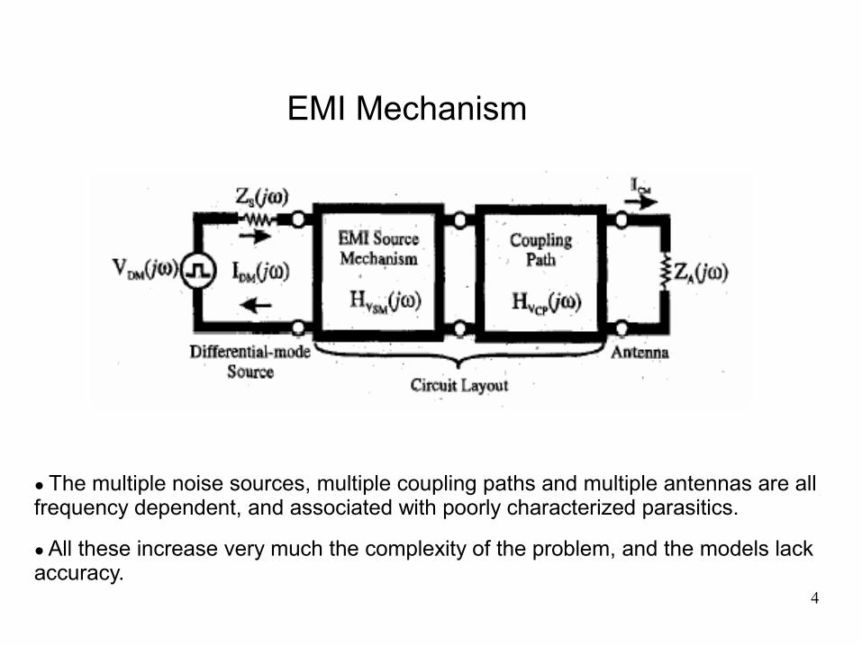
EMI Mechanism
● The multiple noise sources, multiple coupling paths and multiple antennas are all frequency dependent, and associated with poorly characterized parasitics.
● All these increase very much the complexity of the problem, and the models lack accuracy.

5
Shielding Effectiveness
S. E. = 20 log ∣ E e
E i ∣ [ dB ] S. E. = 20 log ∣ H e
H i ∣ [ dB ] S. E. = 10 log ∣ Pe
Pi ∣ [ dB ]
E e = Electric field exteriorE i = Electric field interior
H e = Magnetic field exterior H i = Magnetic field interior
P e = Power exterior P i = Power interior
For external noise source (immunity):

6
Shielding Effectiveness

7
Near Field vs. Far Field for Point Sources
ZW m =dE
dH
=
jr2 − 2
v r
1r 3 j
vr 2 − 2
v2 r
ZW e =dE
dH
= 1
1jr 3 1
v r 2 jv2 r
1r 2
jv r
ZW m =d E
d H
j ω μ r 377 ZW e =d E
d H
1j ω r
377
ZW =dE
dH
= 1 v
= 1
1 μ
= μ μ0
0
= 120 π = 377
Small electric dipole Small electric dipole Small electric dipole Small current loop
Far Field (Radiation Zone, Fraunhoffer Zone):
Near Field (Reactive Field or Fresnel Zone)
0 = 136
10−9 F /m
0 = 4 10−7 H /m
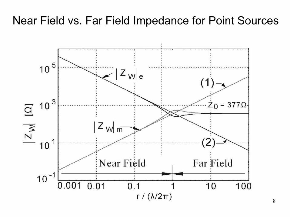
8
Near Field vs. Far Field Impedance for Point Sources

9
Outline
● Introduction: EMI mechanisms, Shielding Effectiveness (SE)
● Basics approaches to shielding: field theory (Kaden) and circuit theory (Schelkunoff)● Limits of the analytical approaches, numerical simulations, reciprocity● Evaluation of shielding materials● Chassis resonances, internal compartmentalization● Slots, apertures, gaskets● Waveguides below cut-off● Understanding the source – local absorbers● Understanding the source – heatsink grounding, chip shielding● Evaluation of shielding effectiveness for a chassis● Local shielding● Shielding and coating issues● Shielding and corrosion issues● Shielding and safety issues
10
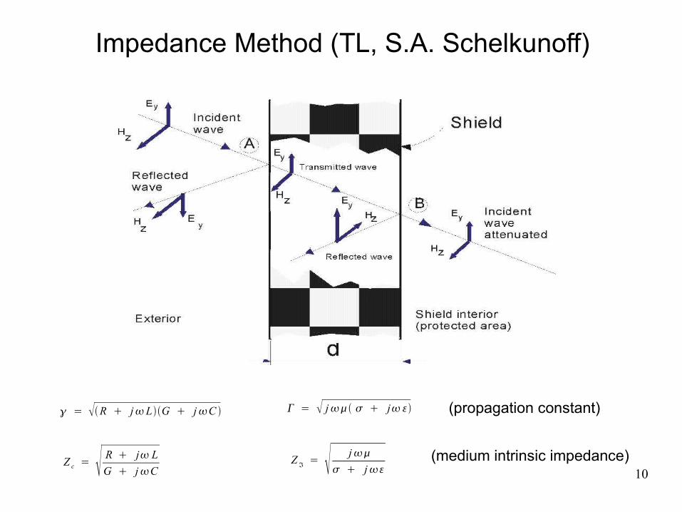
Impedance Method (TL, S.A. Schelkunoff)
= j j = R jLG jC
Z ℑ = j jZ c = R j L
G jC
(propagation constant)
(medium intrinsic impedance)

11
Impedance Method – Reflection Losses
Z1 = μ0
0
= 120 π = 377 []
openspace impedance
Z 2 = j j
[]
shield intrinsic impedance
R = 20 log10 ∣ Z2 Z 12
4Z2 Z 1∣ [dB]
R=Reflection losses

12
Skin Effect & Absorption Losses
A = 8.69 d [dB] Absorption Losses
B = 20 log 1 − e− 2d
[dB] Correction for thin shields
S. E. = A R B [dB ] Shielding Effectiveness
= 2
= 1 f
[ mm ]
Where:δ = skin depth (mm)ω = angular (radian) frequency
μ = material permeability (4π x 10-7 H/m
σ = material conductivity (5.82 x 10⁷ mho/m for Cu)f = frequency (hertz)
d = thickness of the shield (mm)
13
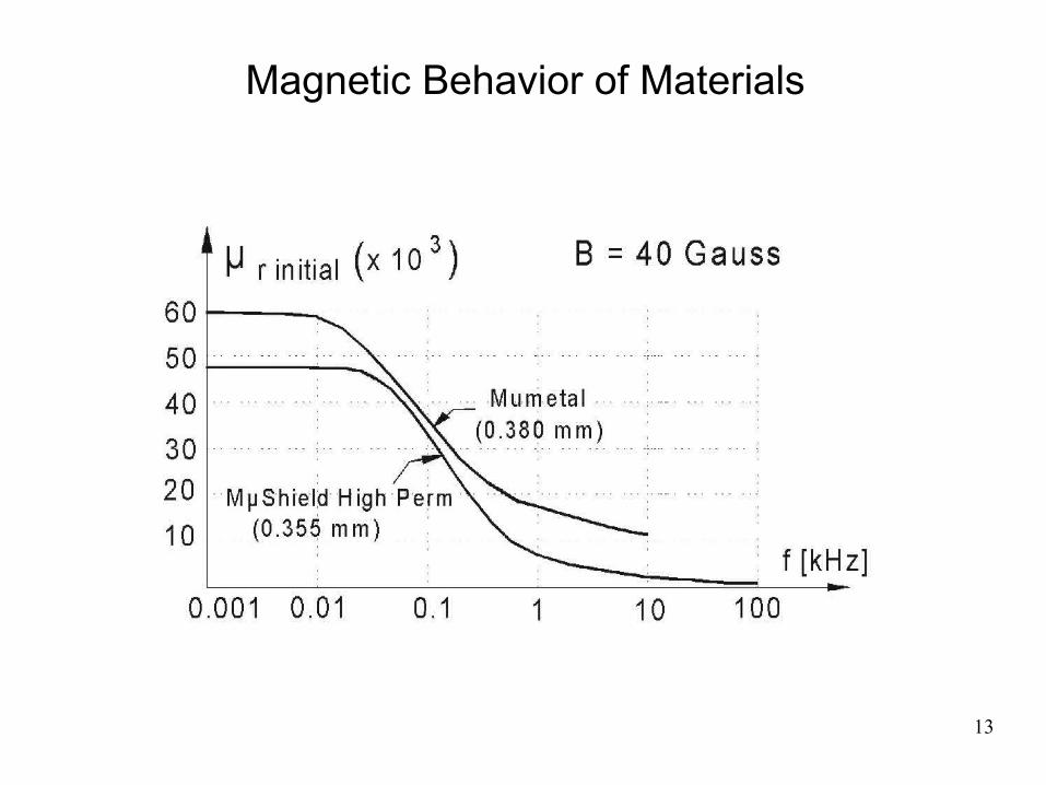
Magnetic Behavior of Materials
14
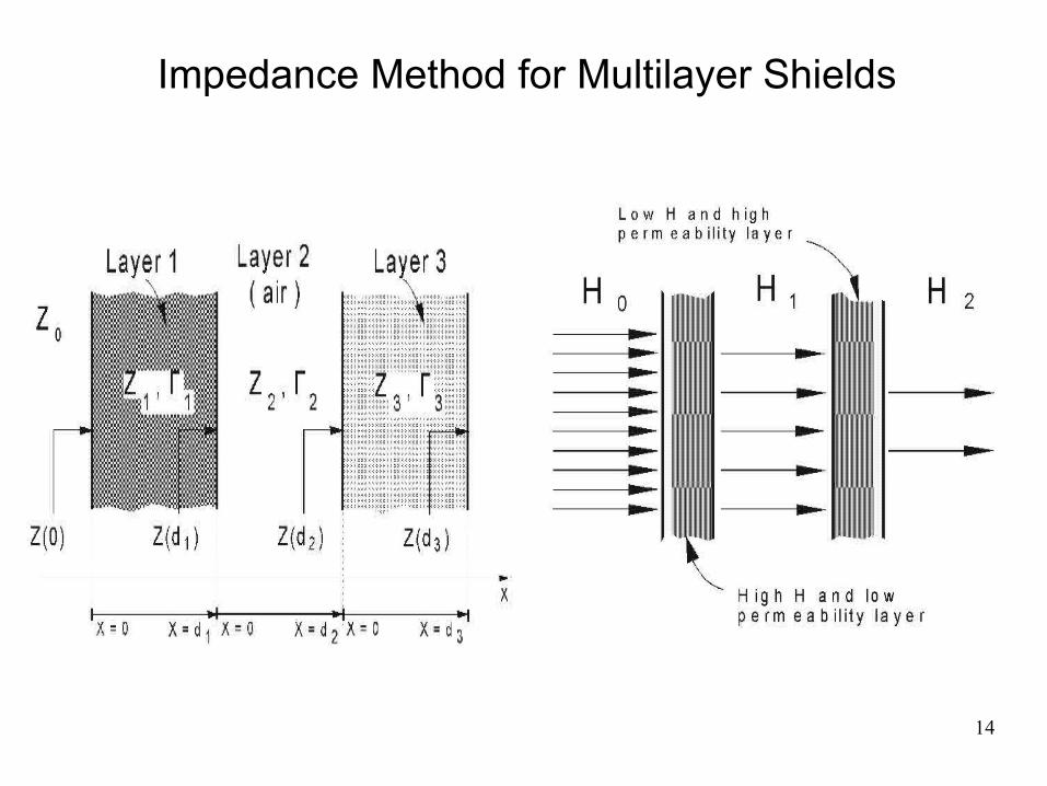
Impedance Method for Multilayer Shields

15
Circuit Method – H. Kaden
Needs continuity of the shield for the circulation of the Eddy currents (Foucault currents)
16
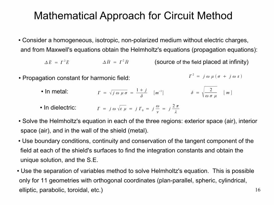
Mathematical Approach for Circuit Method
E = 2 E H = 2 H
2 = j ω μ σ j ω
= j ω μ σ = 1 jδ
[m−1] δ = 2ω σ μ
[ m ]
= j ω μ = j 0 = j ωv
= j 2 πλ
● Consider a homogeneous, isotropic, non-polarized medium without electric charges, and from Maxwell's equations obtain the Helmholtz's equations (propagation equations):
● Propagation constant for harmonic field:
● In metal:
● In dielectric:
● Solve the Helmholtz's equation in each of the three regions: exterior space (air), interior space (air), and in the wall of the shield (metal).
● Use boundary conditions, continuity and conservation of the tangent component of the field at each of the shield's surfaces to find the integration constants and obtain the unique solution, and the S.E.
(source of the field placed at infinity)
● Use the separation of variables method to solve Helmholtz's equation. This is possibleonly for 11 geometries with orthogonal coordinates (plan-parallel, spheric, cylindrical, elliptic, parabolic, toroidal, etc.)

17
Circuit Method Applied for the Plan-Parallel Shield
S. E. [ dB ] = 10 log [ 12 cosh 2 d
cos 2 d
0 x0
sinh 2 d
− sin 2 d 0 x0
2
cosh 2 d
− cos 2 d ]
Parameters: geometry (d, x0), material (σ, μ), frequency (f)

18
Circuit Method Applied for the Spherical Shield
S.E. = 10 log [ 12 cosh 2 d
δ cos 2 d
δ 5 A2 2 B2 − 2 A B 12 cosh 2 d
δ− cos 2 d
δ ...][... A sinh 2 d
δ 2 sin 2 d
δ B sinh 2 dδ
− sin 2 dδ ]
A = μ δ3 μo r o
B =μo r o3 μ δ
δ = 2ω σ μ
Parameters: geometry (d, r0), material (σ, μ), frequency (f)

19
Example of Field Behavior (Spherical Shield)
LF – Magnetic Material (no tangential field)(No shielding effect for non-magnetic)
HF – Magnetic or Non-Magnetic Material(no radial field component on the exterior)
20
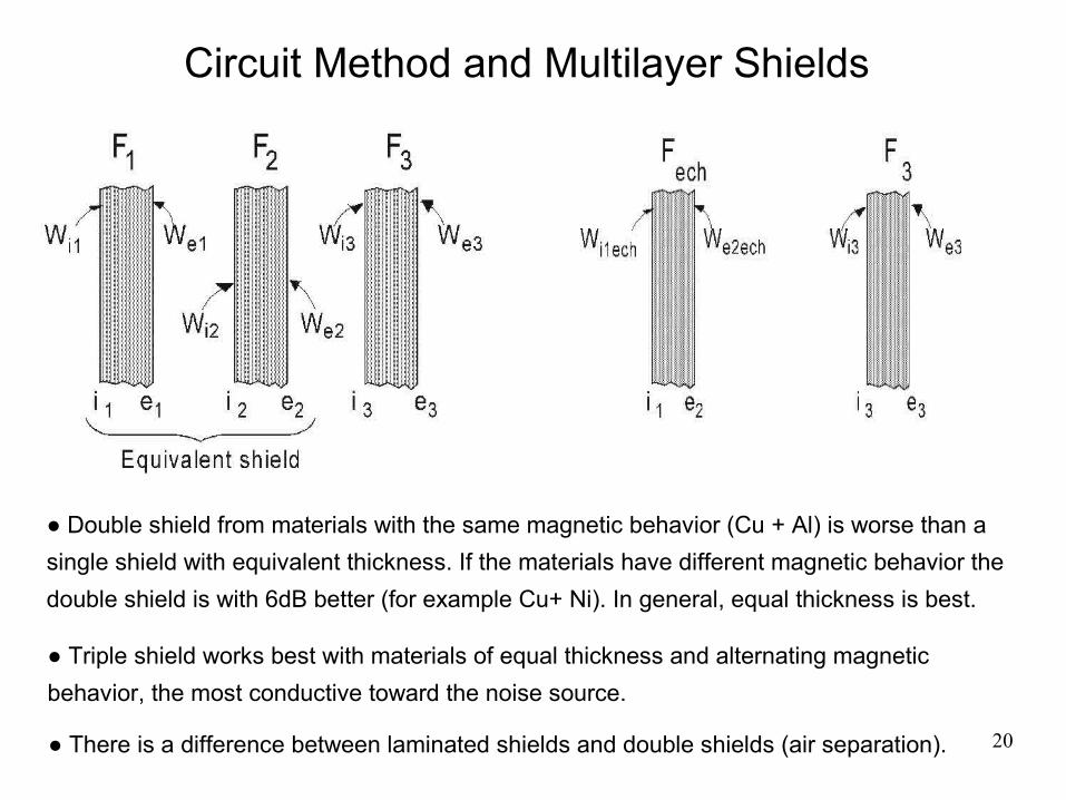
Circuit Method and Multilayer Shields
● Double shield from materials with the same magnetic behavior (Cu + Al) is worse than a single shield with equivalent thickness. If the materials have different magnetic behavior thedouble shield is with 6dB better (for example Cu+ Ni). In general, equal thickness is best.
● Triple shield works best with materials of equal thickness and alternating magnetic behavior, the most conductive toward the noise source.
● There is a difference between laminated shields and double shields (air separation).

21
Outline
● Introduction: EMI mechanisms, Shielding Effectiveness (SE)● Basics approaches to shielding: field theory (Kaden) and circuit theory (Schelkunoff)
● Limits of the analytical approaches, numerical simulations, reciprocity● Evaluation of shielding materials● Chassis resonances, internal compartmentalization● Slots, apertures, gaskets● Waveguides below cut-off● Understanding the source – local absorbers● Understanding the source – heatsink grounding, chip shielding● Evaluation of shielding effectiveness for a chassis● Local shielding● Shielding and coating issues● Shielding and corrosion issues● Shielding and safety issues
22
Limits of the Analytical Methods
● Analytical methods:
• impedance method (Schelkunoff) - infinite sheet of metal
• separation of variables (Kaden) – theoretically possible for 11 geometries)
● Physical insight and precision - perfect as a benchmark for the evaluation of the numerical methods.
● Numerical simulation (FDTD, FEM, MoM, etc.) - can’t be used for real life situations, no physical insight, difficult to characterize the noise source, internal reflections, large size of the file, etc.
● Very good for simple cases to analyze a trend or principle.
● Experimental methods - the only real validation of the analytical or numerical models.
● In the end, all these are about material and thickness of the shield, and to a little extent about the geometry (circuit method).
23
Far Field Estimations using Analytical Methods
● Based on measuring the Q of the enclosure
● Based on the measurement of the field in the aperture and the Huygens principle
● Based on the evaluation of the field in the aperture and Bethe’s theory of diffraction through small holes
● Problems: multiple sources without accurate characterization, multiple coupling paths, and multiple apertures - the real field in the aperture can’t be correctly estimated in early phases of the design.
● The main results: trends and possible estimation of the relative effect of a modification.
● Numerical methods will do correctly the near-field to far-field extrapolation and calculate the field at 10m or 3m without meshing the whole space between the EUT and the antenna.
24
Shielding and Reciprocity● Reciprocity principle is applicable only to passive and linear circuits (a CPU, ASIC, IC is active and non-linear).
● Reciprocity requires us to consider only those parts of the system that meet the criteria of “passiveness” and “linearity”. In this sense, within an electronic system, the properties of radiators/sensors can often be assumed to be reciprocal, just as is the case with antennas.
● In shielding practice, we can find non-linear effects, like the "rusty bolt" effect, which results in nonlinear and non-reversible conductivity (diode). Another typical example from shielding practice, is a multilayer shield, with one of the layers having nonlinear magnetic permeability.
● If the shield is linear, the reciprocity principle requires that Z21
=Z12
. The same requirements for passive, linear, circuits hold. As long as the shield is a passive network and its material exhibits linear electric and magnetic properties, the reciprocity theorem holds, and the same shielding parameters are true for emissions and susceptibility. However, this is true only at the levels of the shield transfer function, but not at the system level shielding effectiveness.
● For example, a dominant radiator in the system (emissions case) is not necessarily the dominant victim in the same system (immunity case). For instance, one of the reasons that the radiator is dominant for emissions may be a high level of signal within it which, on the other hand, makes this particular part of the system more immune to EMI. Typically, the Tx (transmitting) output signal is 20dB stronger than Rx (receiving) input signal.
25
Outline
● Introduction: EMI mechanisms, Shielding Effectiveness (SE)● Basics approaches to shielding: field theory (Kaden) and circuit theory (Schelkunoff)● Limits of the analytical approaches, numerical simulations, reciprocity● Evaluation of shielding materials● Chassis resonances, internal compartmentalization● Slots, apertures, gaskets● Waveguides below cut-off● Understanding the source – local absorbers● Understanding the source – heatsink grounding, chip shielding● Evaluation of shielding effectiveness for a chassis● Local shielding● Shielding and coating issues● Shielding and corrosion issues● Shielding and safety issues
26
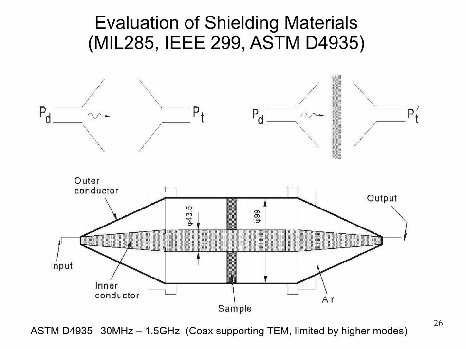
Evaluation of Shielding Materials (MIL285, IEEE 299, ASTM D4935)
ASTM D4935 30MHz – 1.5GHz (Coax supporting TEM, limited by higher modes)
27
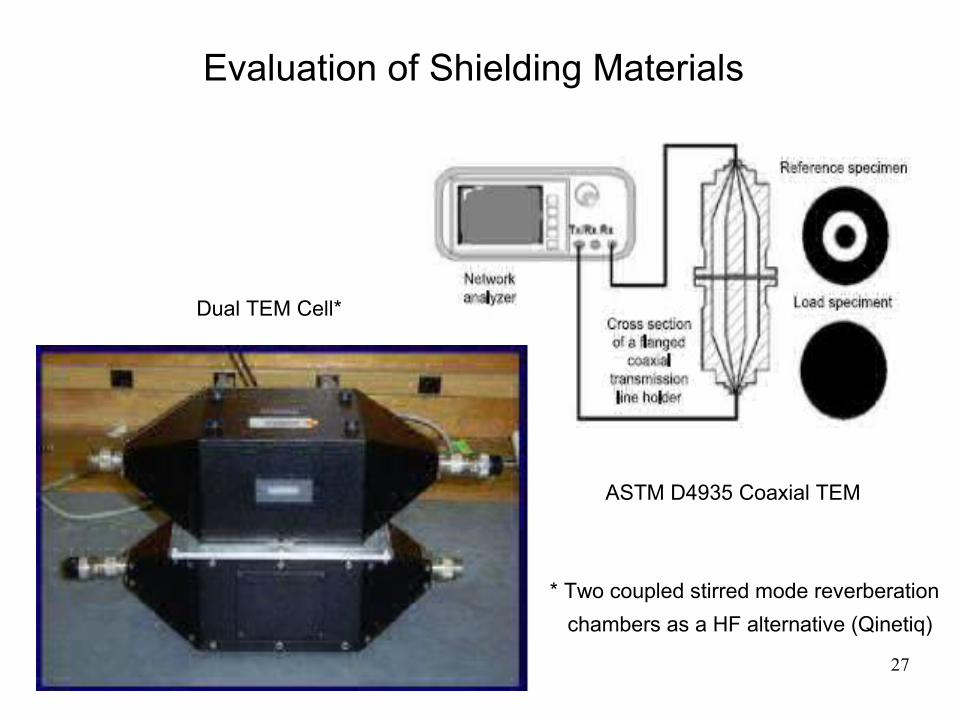
Evaluation of Shielding Materials
Dual TEM Cell*
ASTM D4935 Coaxial TEM
* Two coupled stirred mode reverberation chambers as a HF alternative (Qinetiq)

28
IEEE 299 – Measuring SE of Enclosures
Schematic diagram of the test configuration for magnetic testsshowing dimensions of transmit (TX) and receive (RX) antennas
Measurement setup for frequencies >1 GHz

29
Experimental Setup
(Antenna too big compared with the volume of the box)
30
Outline
● Introduction: EMI mechanisms, Shielding Effectiveness (SE)● Basics approaches to shielding: field theory (Kaden) and circuit theory (Schelkunoff)● Limits of the analytical approaches, numerical simulations, reciprocity● Evaluation of shielding materials
● Chassis resonances, internal compartmentalization● Slots, apertures, gaskets● Waveguides below cut-off● Understanding the source – local absorbers● Understanding the source – heatsink grounding, chip shielding● Evaluation of shielding effectiveness for a chassis● Local shielding● Shielding and coating issues● Shielding and corrosion issues● Shielding and safety issues
31
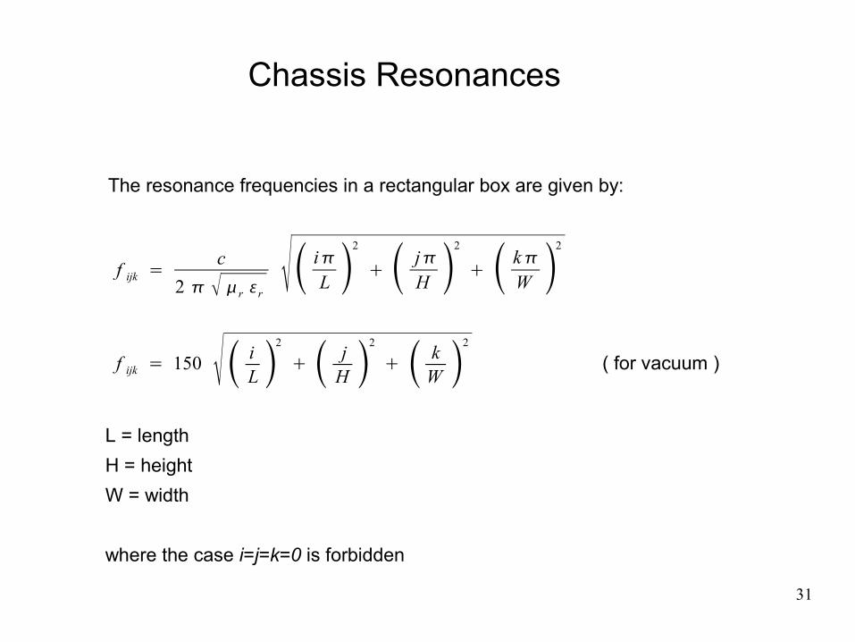
Chassis Resonances
The resonance frequencies in a rectangular box are given by:
L = lengthH = heightW = width
where the case i=j=k=0 is forbidden
f ijk = c2 r r i
L 2
jH
2
kW
2
f ijk = 150 iL
2
jH
2
kW
2
( for vacuum )

32
Rectangular Box - Lowest Resonance Frequencies
f0
0
3.368 108.
6.737 108.
1.011 109.
8.605 108.
9.241 108.
1.093 109.
1.327 109.
1.721 109.
1.754 109.
1.848 109.
1.996 109.
2.581 109.
2.603 109.
2.668 109.
2.772 109.
=
f1
2.231 108.
4.041 108.
7.097 108.
1.035 109.
8.889 108.
9.506 108.
1.115 109.
1.346 109.
1.735 109.
1.768 109.
1.862 109.
2.008 109.
2.591 109.
2.613 109.
2.677 109.
2.781 109.
=
f2
4.463 108.
5.591 108.
8.081 108.
1.105 109.
9.693 108.
1.026 109.
1.18 109.
1.4 109.
1.778 109.
1.81 109.
1.901 109.
2.045 109.
2.62 109.
2.641 109.
2.705 109.
2.808 109.
=
f3
6.694 108.
7.494 108.
9.497 108.
1.212 109.
1.09 109.
1.141 109.
1.282 109.
1.487 109.
1.847 109.
1.877 109.
1.966 109.
2.105 109.
2.667 109.
2.688 109.
2.751 109.
2.852 109.
=
● At higher frequency (for example >1GHz), the enclosure supports a very large number of modes. Lowest modes: 223, 336, 404, 446, 559, 669, 673, ... MHz.
● An empty box has very high Q, very sharp resonances. The energy stored is proportional to volume, and losses are proportional with the surface area.

33
Field Distributions at Resonant Frequencies
HzXZ
TMy201 - Ey(x,z) (rear)
EyXZ
TMy201 - Hx(x,z) (rear)
HxXZ
HxXZ
HzXZ
● Empty box: Q=5000, Fully loaded, densely populated box: Q=5-25 (practical implications)
● Use extensively internal compartmentalization (limit excitations, lower Q, higher fres
)
34
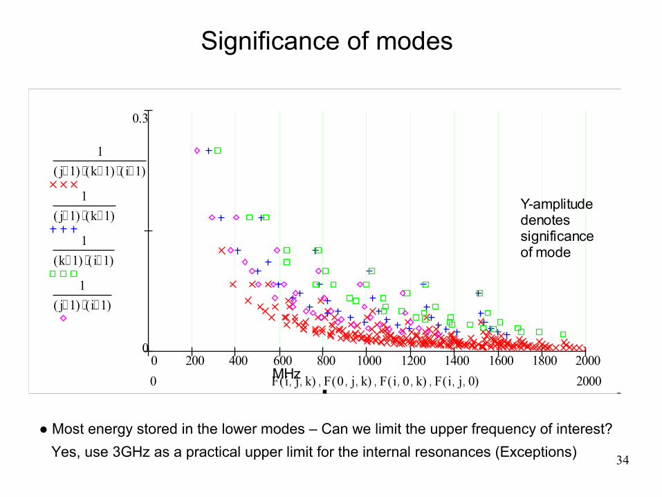
Significance of modes
0 200 400 600 800 1000 1200 1400 1600 1800 2000
0.3
0
1j 1+( ) k 1+( )⋅ i 1+( )⋅
1j 1+( ) k 1+( )⋅
1k 1+( ) i 1+( )⋅
1j 1+( ) i 1+( )⋅
20000 F i j, k,( ) F 0 j, k,( ), F i 0, k,( ), F i j, 0,( ),
Y-amplitudedenotessignificanceof mode
MHz
● Most energy stored in the lower modes – Can we limit the upper frequency of interest? Yes, use 3GHz as a practical upper limit for the internal resonances (Exceptions)
35
Outline
● Introduction: EMI mechanisms, Shielding Effectiveness (SE)● Basics approaches to shielding: field theory (Kaden) and circuit theory (Schelkunoff)● Limits of the analytical approaches, numerical simulations, reciprocity● Evaluation of shielding materials● Chassis resonances, internal compartmentalization
● Slots, apertures, gaskets● Waveguides below cut-off● Understanding the source – local absorbers● Understanding the source – heatsink grounding, chip shielding● Evaluation of shielding effectiveness for a chassis● Local shielding● Shielding and coating issues● Shielding and corrosion issues● Shielding and safety issues

36
Why Apertures Radiate?

37
Why joints radiate?
● Similar behavior for screws & rivets
38
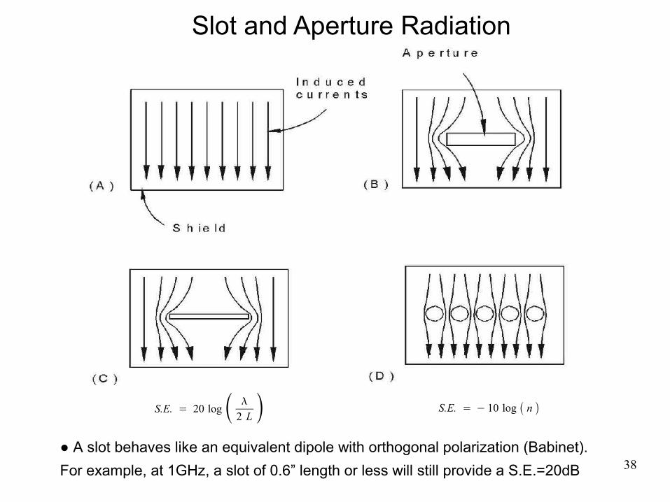
Slot and Aperture Radiation
S.E. = 20 log 2 L S.E. = − 10 log n
● A slot behaves like an equivalent dipole with orthogonal polarization (Babinet).For example, at 1GHz, a slot of 0.6” length or less will still provide a S.E.=20dB

39
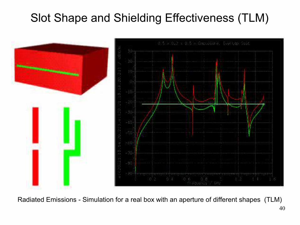
Slot Shape and Shielding Effectiveness (TLM)
Slot resonant at 3.6GHz, SE at 5 cm away from the slot
Shape C
Shape B
Shape A
40
Slot Shape and Shielding Effectiveness (TLM)
Radiated Emissions - Simulation for a real box with an aperture of different shapes (TLM)

41
Example of joint treatment for a lid
● Can we avoid gaskets?
42
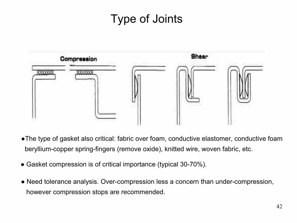
Type of Joints
● Gasket compression is of critical importance (typical 30-70%).
● Need tolerance analysis. Over-compression less a concern than under-compression, however compression stops are recommended.
●The type of gasket also critical: fabric over foam, conductive elastomer, conductive foam beryllium-copper spring-fingers (remove oxide), knitted wire, woven fabric, etc.
43
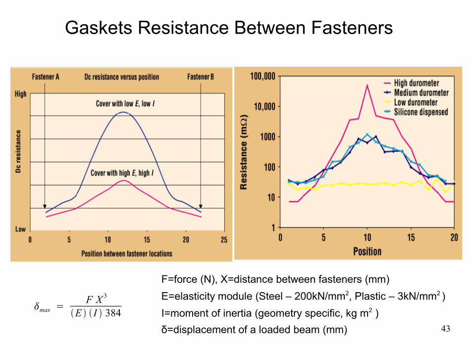
Gaskets Resistance Between Fasteners
F=force (N), X=distance between fasteners (mm)E=elasticity module (Steel – 200kN/mm2, Plastic – 3kN/mm2 )I=moment of inertia (geometry specific, kg m2 )δ=displacement of a loaded beam (mm)
max = F X 3
E I 384

44
Example of gasketing for a lid and rivets
45
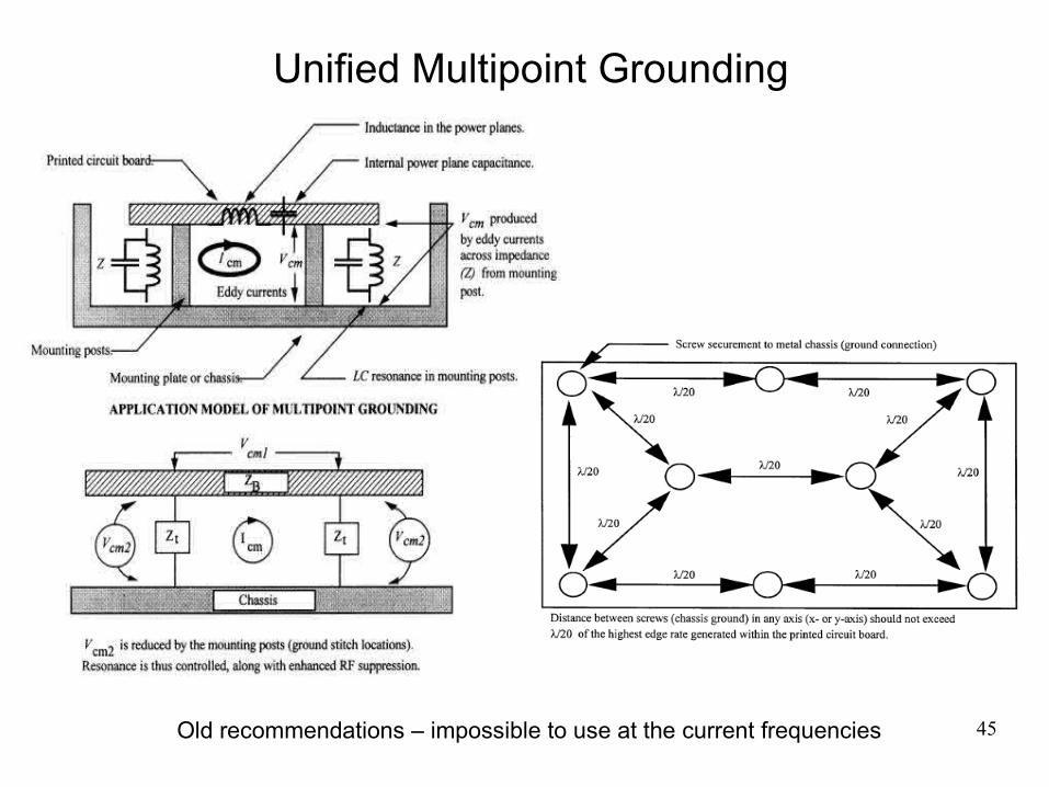
Unified Multipoint Grounding
Old recommendations – impossible to use at the current frequencies
46
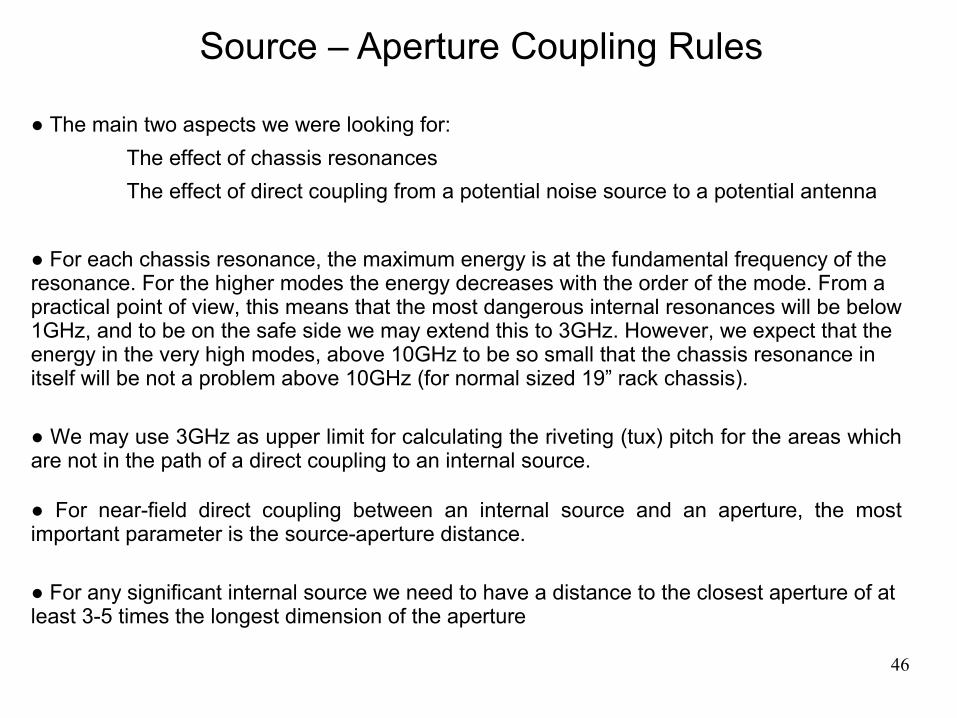
● The main two aspects we were looking for: The effect of chassis resonancesThe effect of direct coupling from a potential noise source to a potential antenna
● For each chassis resonance, the maximum energy is at the fundamental frequency of the resonance. For the higher modes the energy decreases with the order of the mode. From a practical point of view, this means that the most dangerous internal resonances will be below 1GHz, and to be on the safe side we may extend this to 3GHz. However, we expect that the energy in the very high modes, above 10GHz to be so small that the chassis resonance in itself will be not a problem above 10GHz (for normal sized 19” rack chassis).
● We may use 3GHz as upper limit for calculating the riveting (tux) pitch for the areas which are not in the path of a direct coupling to an internal source.
● For near-field direct coupling between an internal source and an aperture, the most important parameter is the source-aperture distance.
● For any significant internal source we need to have a distance to the closest aperture of at least 3-5 times the longest dimension of the aperture
Source – Aperture Coupling Rules
47
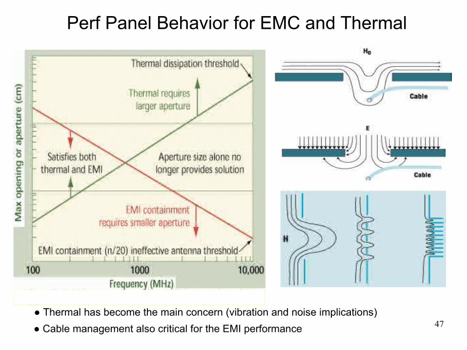
Perf Panel Behavior for EMC and Thermal
● Thermal has become the main concern (vibration and noise implications)● Cable management also critical for the EMI performance

48
Outline
● Introduction: EMI mechanisms, Shielding Effectiveness (SE)● Basics approaches to shielding: field theory (Kaden) and circuit theory (Schelkunoff)● Limits of the analytical approaches, numerical simulations, reciprocity● Evaluation of shielding materials● Chassis resonances, internal compartmentalization● Slots, apertures, gaskets● Waveguides below cut-off● Understanding the source – local absorbers● Understanding the source – heatsink grounding, chip shielding● Evaluation of shielding effectiveness for a chassis● Local shielding● Shielding and coating issues● Shielding and corrosion issues● Shielding and safety issues

49
Effect of Perf – Wire Coupling on Shielding
Wire at 20 mm from the hole for single holes

50
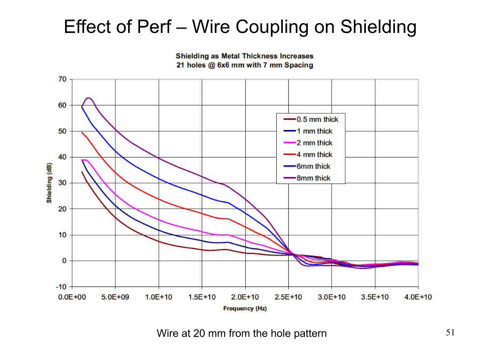
Effect of Perf – Wire Coupling on Shielding
Wire at 20 mm from the hole pattern
51
Effect of Perf – Wire Coupling on Shielding
Wire at 20 mm from the hole pattern

52
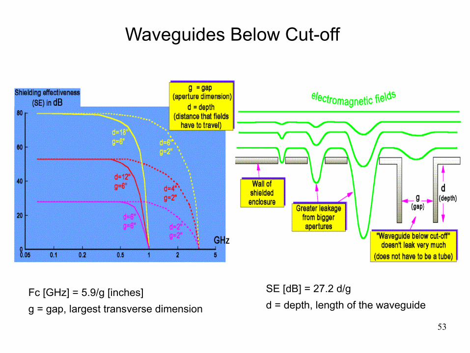
Waveguides Below Cut-off
f cc = 175.768D [ m ] [ MHz ] f cr = 150.114
W [ m ] [ MHz ]
S.E.c = 32Lc
D [ dB ] S.E.r = 27.2Lr
W [ dB ]
S.E.≃ 27 La − 20 log10 N [ dB ]● For Honeycomb:
where: a - the largest waveguide transverse dimension, L – the length of the waveguide,and N – the number of waveguides employed in the honeycomb
● Never pass a wire through a waveguide below cutoff (will support TEM mode)
53
Waveguides Below Cut-off
Fc [GHz] = 5.9/g [inches]g = gap, largest transverse dimension
SE [dB] = 27.2 d/gd = depth, length of the waveguide

54
Honeycomb – Air Pressure Drop and SE
T = length of the waveguide, depthW = the largest transverse dimension
55
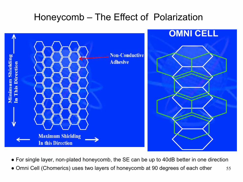
Honeycomb – The Effect of Polarization
● For single layer, non-plated honeycomb, the SE can be up to 40dB better in one direction● Omni Cell (Chomerics) uses two layers of honeycomb at 90 degrees of each other

56
An Example: Single Layer 1/4” Honeycomb

57
Honeycomb Frames & Gaskets
T = length of the waveguide, depth

58
Perf Panel Example
SE = 8dB @ 1.2GHz
I
It gets worse if the frequency,diameter or panel dimensions increase, or if center distances decrease.
For a 1/4” plated honeycombwith less than 1/4” cells: SE > 50dB @ 10GHz
SE = 8dB @ 1.2GHz
For staggered round holes with 4mm diameter, and center to center distance of 4.7mm, for a 92x206mm panel:
SE = 13dB @ 1.2GHz
SE = 8dB @ 1.2GHz
(Type of perf pattern used in some power supplies)

59
Typical Perf Used for Cosmetic Areas
60
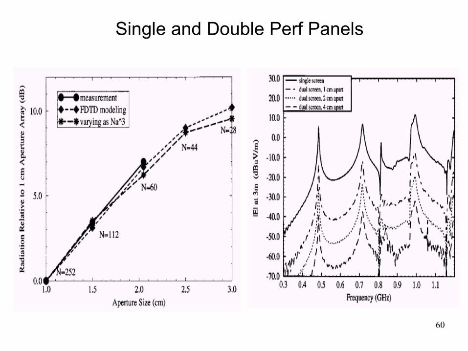
Single and Double Perf Panels
61
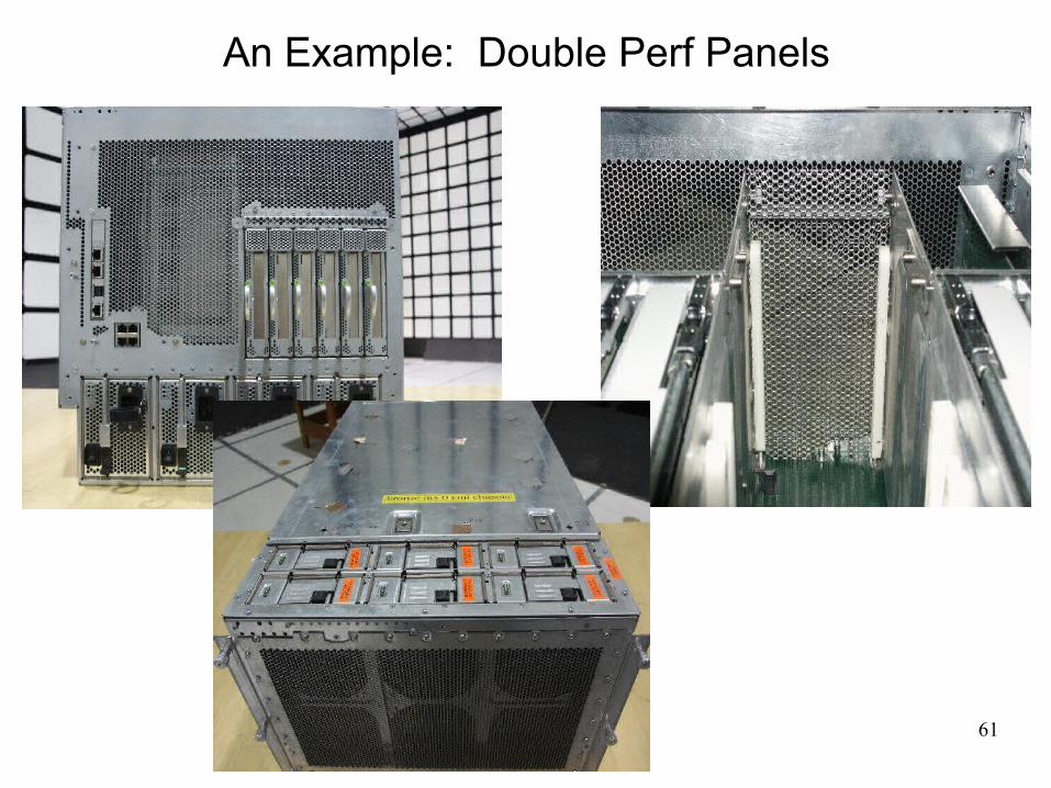
An Example: Double Perf Panels
62
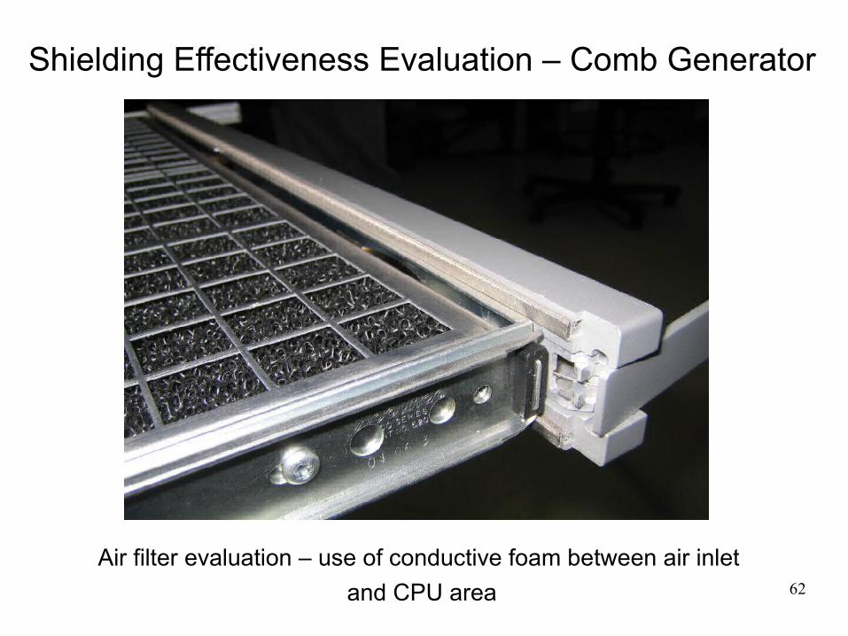
Shielding Effectiveness Evaluation – Comb Generator
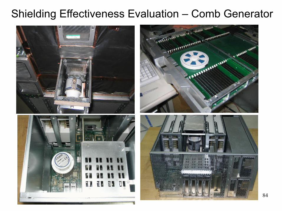
Air filter evaluation – use of conductive foam between air inlet and CPU area
63
Outline
● Introduction: EMI mechanisms, Shielding Effectiveness (SE)● Basics approaches to shielding: field theory (Kaden) and circuit theory (Schelkunoff)● Limits of the analytical approaches, numerical simulations, reciprocity● Evaluation of shielding materials● Chassis resonances, internal compartmentalization● Slots, apertures, gaskets● Waveguides below cut-off
● Understanding the source – local absorbers● Understanding the source – heatsink grounding, chip shielding● Evaluation of shielding effectiveness for a chassis● Local shielding● Shielding and coating issues● Shielding and corrosion issues● Shielding and safety issues
64
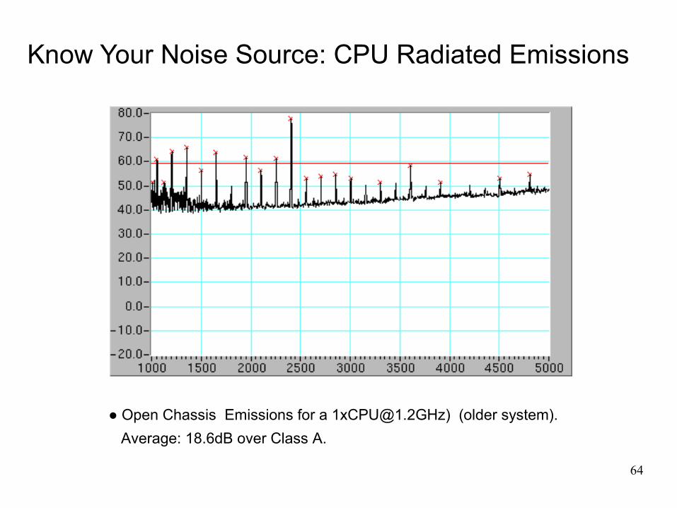
Know Your Noise Source: CPU Radiated Emissions
● Open Chassis Emissions for a [email protected]) (older system). Average: 18.6dB over Class A.

65
EMI mechanisms for VLSI chips
● The Heatsink acting as a monopole antenna against the first solid plane of the PCB (tall Heatsink).
● The Heatsink and the first solid plane of the PCB creating a patch antenna (wide Heatsink).
● The low inductance power distribution of the VLSI chip allows noise injection into the PCB, which re-radiates (especially through closely placed DC-DC converters).

66
Typical problems with heatsink grounding
● Components on Top need to be placed at a distance (some decoupling may be impacted)
● No pin escapes on Top
● The routing might be impacted by the multiple vias from the GND ring to GND plane
● Not effective above approx. 1GHz (any grounding will be too inductive to really matter)
● No direct DC grounding if the chip can use Back Bias or Forward Bias
67
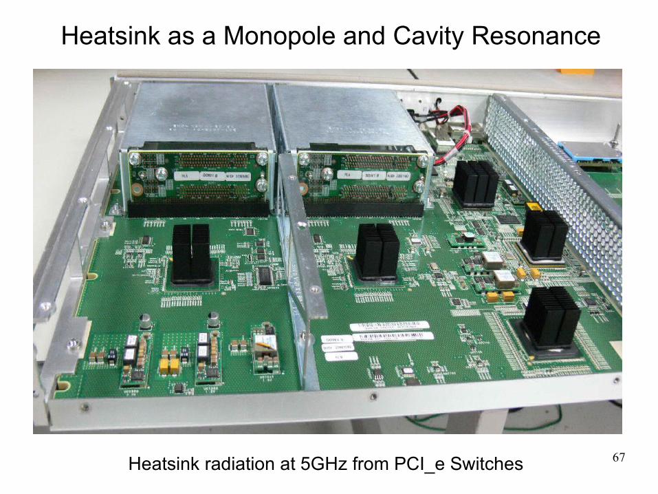
Heatsink as a Monopole and Cavity Resonance
Heatsink radiation at 5GHz from PCI_e Switches

68
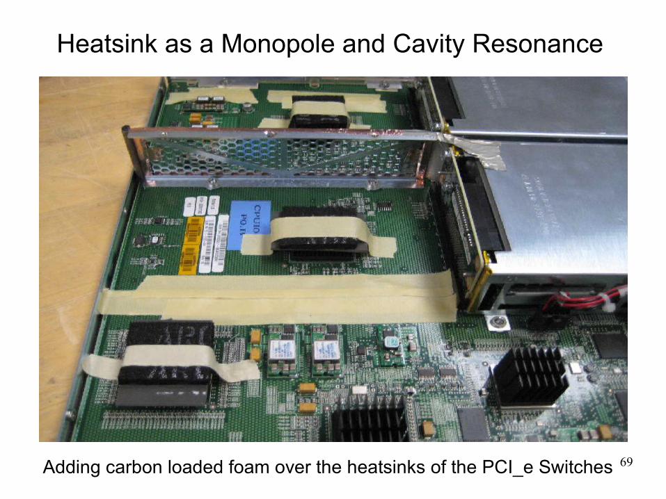
Heatsink as a Monopole and Cavity Resonance
Removing the heatsinks from the PCI_e switches, 5GHz decreases
69
Heatsink as a Monopole and Cavity Resonance
Adding carbon loaded foam over the heatsinks of the PCI_e Switches

70
Electromagnetic Wave Absorbers
P = P P P = 12 ∣E ∣2 1
2 0 1 ' ' ∣E ∣
2 12 0 1 ' ' ∣H ∣ 2
● Electromagnetic wave absorption materials absorb the energy in electromagnetic waves as resistive, dielectric or magnetic losses, and convert that energy, in the end, to heat. The amount of that absorption, P, can be expressed by the following formula:
P [W/m3]: Electromagnetic energy absorbed per unit volume
E [V/m]: Electric field strength of the incident electromagnetic radiation
H [A/m]: Magnetic field strength of the incident electromagnetic radiation
σ [S/m]: Conductivity of the material
ω [sec-1]: Angular speed of the electromagnetic wave (= 2πf)
εr″(ω): Complex component of the dielectric constant of the material ε
r(ω) = ε
r'(ω) + jε
r″(ω)
ε0 [F/m]: Dielectric constant of the vacuum: 8.854 × 10⁻¹² [F/m]
μr″(ω): Complex component of the dielectric constant of the material μ
r(ω) = μ
r'(ω) - jμ
r″(ω)
μ0 [A/m]: Magnetic permeability of the vacuum: 1.2566 × 10⁻⁶ [H/m]
εr″(ω), μ
r″(ω) – related to losses (dissipation), ε
r'(ω), μ
r'(ω) – related to stored energy within the medium
71
Outline
● Introduction: EMI mechanisms, Shielding Effectiveness (SE)● Basics approaches to shielding: field theory (Kaden) and circuit theory (Schelkunoff)● Limits of the analytical approaches, numerical simulations, reciprocity● Evaluation of shielding materials● Chassis resonances, internal compartmentalization● Slots, apertures, gaskets● Waveguides below cut-off● Understanding the source – local absorbers
● Understanding the source – heatsink grounding, chip shielding● Evaluation of shielding effectiveness for a chassis● Local shielding● Shielding and coating issues● Shielding and corrosion issues● Shielding and safety issues
72
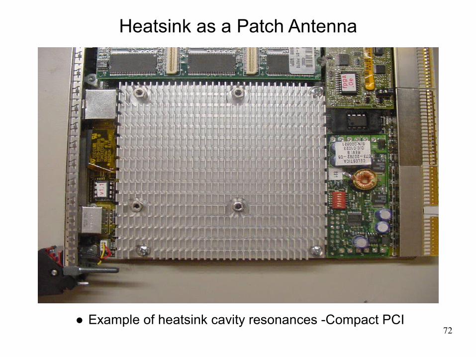
Heatsink as a Patch Antenna
● Example of heatsink cavity resonances -Compact PCI
73
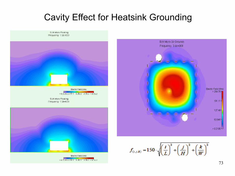
Cavity Effect for Heatsink Grounding

74
Heatsink: Grounding vs. Shielding
● Grounding will work at lower frequencies, but not above 1GHz
● Heatsink shielding works at higher frequency (grounding is implicit)if the contact is continuous, 360 degrees, creating a Faraday cage.

75
Typical Heatsink Grounding and Shielding
● Grounding ring and EMI gasket on top layer PCB
76
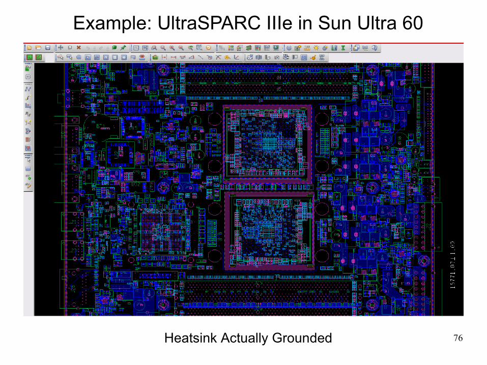
Example: UltraSPARC IIIe in Sun Ultra 60
Heatsink Actually Grounded

77
VLSI injecting noise into the PCB
● μPGA (more inductive) and LGA (less inductive)
78
Outline
● Introduction: EMI mechanisms, Shielding Effectiveness (SE)● Basics approaches to shielding: field theory (Kaden) and circuit theory (Schelkunoff)● Limits of the analytical approaches, numerical simulations, reciprocity● Evaluation of shielding materials● Chassis resonances, internal compartmentalization● Slots, apertures, gaskets● Waveguides below cut-off● Understanding the source – local absorbers● Understanding the source – heatsink grounding, chip shielding● Evaluation of shielding effectiveness for a chassis● Local shielding● Shielding and coating issues● Shielding and corrosion issues● Shielding and safety issues
79
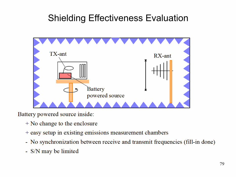
Shielding Effectiveness Evaluation
80
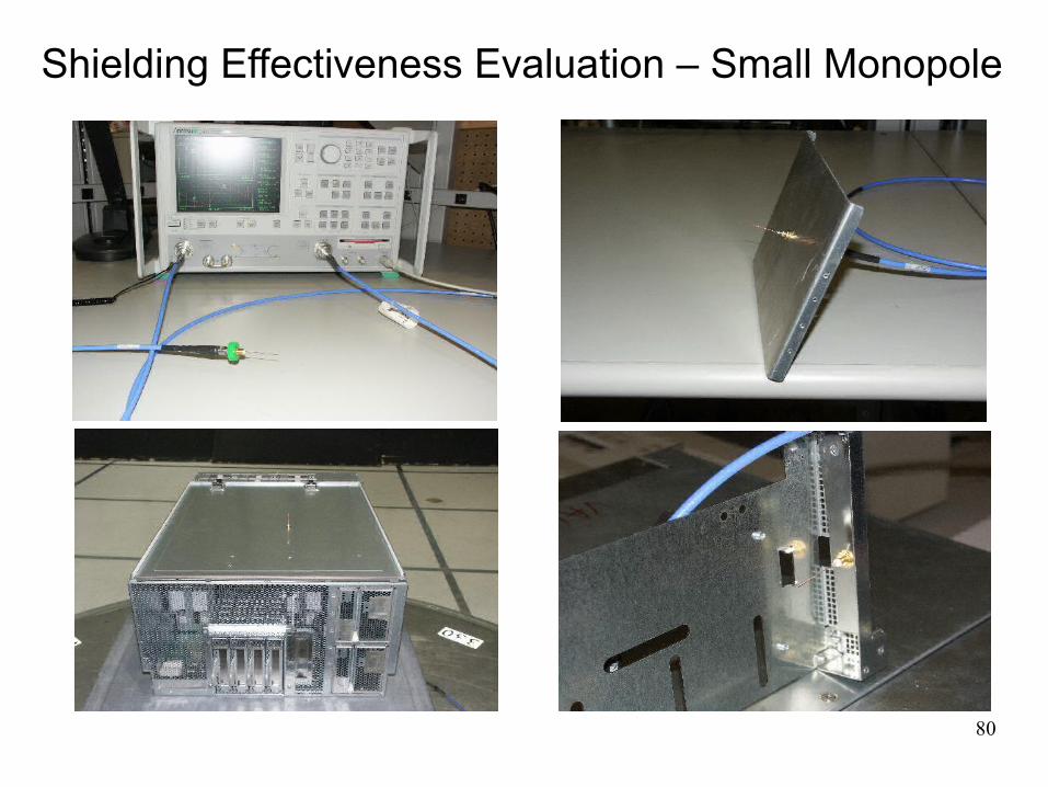
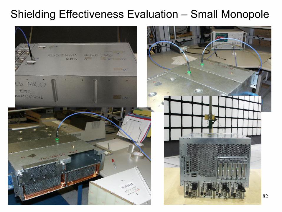
Shielding Effectiveness Evaluation – Small Monopole
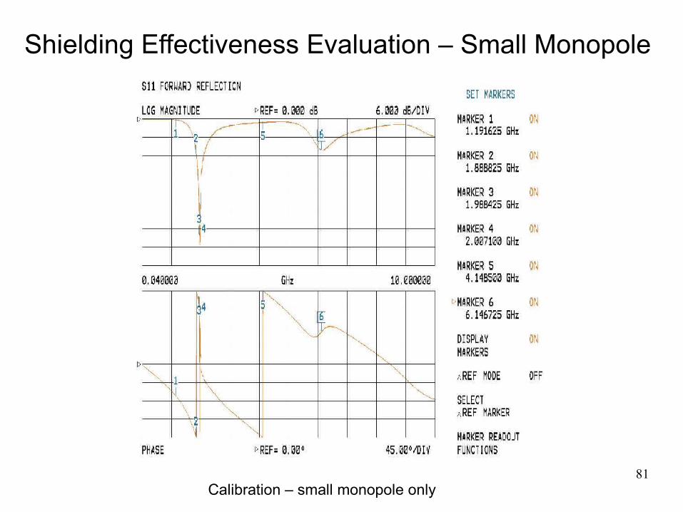
81
Shielding Effectiveness Evaluation – Small Monopole
Calibration – small monopole only
82
Shielding Effectiveness Evaluation – Small Monopole

83
Shielding Effectiveness Evaluation – Comb Generator
84
Shielding Effectiveness Evaluation – Comb Generator
85
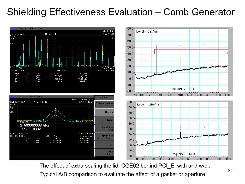
Shielding Effectiveness Evaluation – Comb Generator
The effect of extra sealing the lid, CGE02 behind PCI_E, with and w/o . Typical A/B comparison to evaluate the effect of a gasket or aperture.
86
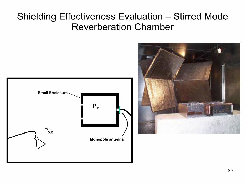
Small Enclosure
Pin
Pout
Monopole antenna
Small Enclosure
Pin
Pout
Monopole antenna
Shielding Effectiveness Evaluation – Stirred Mode Reverberation Chamber

87
Outline
● Introduction: EMI mechanisms, Shielding Effectiveness (SE)● Basics approaches to shielding: field theory (Kaden) and circuit theory (Schelkunoff)● Limits of the analytical approaches, numerical simulations, reciprocity● Evaluation of shielding materials● Chassis resonances, internal compartmentalization● Slots, apertures, gaskets● Waveguides below cut-off● Understanding the source – local absorbers● Understanding the source – heatsink grounding, chip shielding● Evaluation of shielding effectiveness for a chassis
● Local shielding● Shielding and coating issues● Shielding and corrosion issues● Shielding and safety issues

88
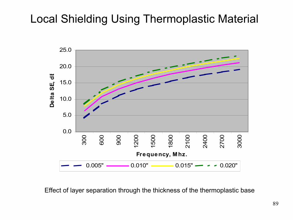
Local Shielding Using Thermoplastic Material
Best results with multilayer shield: Steel (2μm)-Copper (4μm)-Steel (2μm)PVC support: 25 mils
Memory harmonics <1GHz (x266MHz)Grounding is critical
89
0.0
5.0
10.0
15.0
20.0
25.0
300
600
900
1200
1500
1800
2100
2400
2700
3000
Frequency, Mhz.
De
lta
SE,
dB
0.005" 0.010" 0.015" 0.020"
Local Shielding Using Thermoplastic Material
Effect of layer separation through the thickness of the thermoplastic base

90
Outline
● Introduction: EMI mechanisms, Shielding Effectiveness (SE)● Basics approaches to shielding: field theory (Kaden) and circuit theory (Schelkunoff)● Limits of the analytical approaches, numerical simulations, reciprocity● Evaluation of shielding materials● Chassis resonances, internal compartmentalization● Slots, apertures, gaskets● Waveguides below cut-off● Understanding the source – local absorbers● Understanding the source – heatsink grounding, chip shielding● Evaluation of shielding effectiveness for a chassis● Local shielding
● Shielding and coating issues● Shielding and corrosion issues● Shielding and safety issues
91
Shield Coating and RoHS
● RoHS requires less than 0.1% Hexavalent Chromium present as an 'homogeneous material', not intentionally added.
● Forms of chromium that are RoHS compliant: pure chrome plating (shiny, metallic), trivalent chromium conversion coatings (“Clear” or “Clear blue bright”).
● “Safe” substitutions for hexavalent chromium conversion coatings for steel:● Use aluminized steel (T2-65 or T2-LC), not galvanized (electro-galvanized steel is
linked to zinc whiskers, but also NEBS GR78 CORE compliance prohibits the use of ANY zinc in our systems, even as an alloying element over 15%)
● If EMI is not an issue, phosphatizing and painting is also an option● If NEBS compliance not an issue, then use “Clear blue bright” trivalent chromium
with acid bath electrolytic zinc underplate: “Zinc plate per ASTM B-633 SCI Type III with clear trivalent chromate conversion coating. Must withstand min. 96 hr ASTM B-166 Salt Spray. No additional dips or coatings.”

92
● Things to watch for with the trivalent chromium coating:
● Some less-than-reputable coaters will try to get away with a hexavalent (or trivalent) chromium conversion coating to which they add a blue dye to make it look like the clear blue bright trivalent. In reality, the blue color comes from added cobalt to the trivalent coating bath, which also enhances the corrosion resistance. We may need to send samples for an external hex chrome "spot check" at a lab to be sure.
● There should be no additional top coats over the clear blue bright trivalent chromium finish. Any additional top coat will most likely be organic and will interfere with the EMI attenuating properties. A surface resistivity check can likely determine the presence of a top coat.
● For aluminum:● Determine if a coating is really needed● If a coating is needed, preferred use is trivalent chromium coating
● NOTE: If EMI is not an issue, anodizing is also an option
Coating

93
Coating
● Chromate type conversion coatings have been observed to require around 20 psi to obtain low readings. Even then, in comparison to bright tin, the resistivity is high.
● Chromate on aluminum has been measured to be around 170 milliohms at 20 psi, while bright tin on aluminum has been observed to be less than 10 milliohms at only 8 psi. Very important above few GHz.
● There is data that shows the surface contact resistance to be several hundreds of milliohms and does not reduce down to below 30 milliohms until a pressure of around 200-250 psi for a nickel coating on aluminum (because of oxide).
● Use mechanical stops either stamped into or bends added to prevent exceeding the maximum compression value, typically 90-95% of the gasket height.

94
Coating
● The coating must pass multiple type of tests: Conductivity, Anti-Finger printing test, Adhesive tape testing without peel off, Good corrosion resistance, Stamp / Paintability Test(scratch and peel off), Humidity Test (60oC / 95%H / 192 hours) without Blister or Rust, Anti-Chemical Resistance.
95
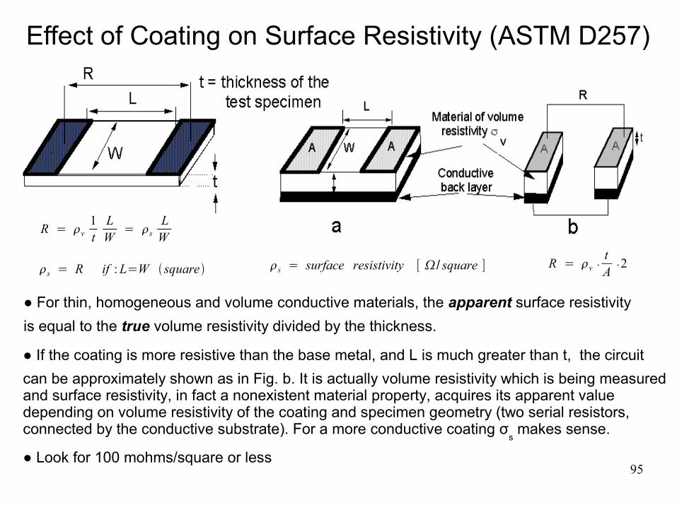
Effect of Coating on Surface Resistivity (ASTM D257)
R = v1t
LW = s
LW
s = R if :L=W square s = surface resistivity [ / square ]
● For thin, homogeneous and volume conductive materials, the apparent surface resistivity is equal to the true volume resistivity divided by the thickness.
R = v ˙tA ˙2
● If the coating is more resistive than the base metal, and L is much greater than t, the circuit can be approximately shown as in Fig. b. It is actually volume resistivity which is being measured and surface resistivity, in fact a nonexistent material property, acquires its apparent value depending on volume resistivity of the coating and specimen geometry (two serial resistors, connected by the conductive substrate). For a more conductive coating σ
s makes sense.
● Look for 100 mohms/square or less
96
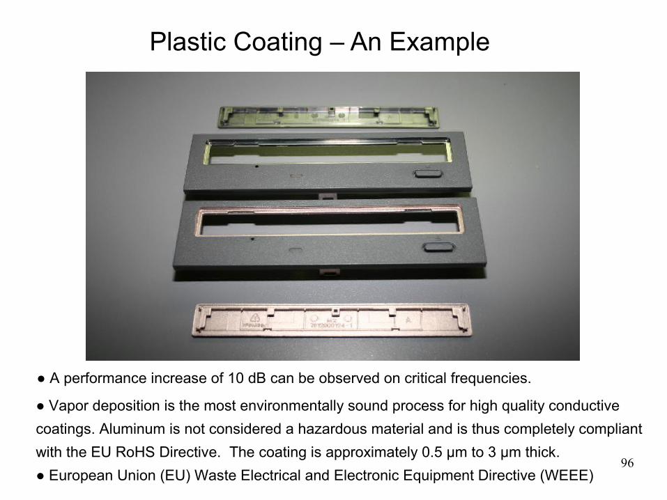
Plastic Coating – An Example
● A performance increase of 10 dB can be observed on critical frequencies.
● Vapor deposition is the most environmentally sound process for high quality conductive coatings. Aluminum is not considered a hazardous material and is thus completely compliant with the EU RoHS Directive. The coating is approximately 0.5 μm to 3 μm thick. ● European Union (EU) Waste Electrical and Electronic Equipment Directive (WEEE)
97
Outline
● Introduction: EMI mechanisms, Shielding Effectiveness (SE)● Basics approaches to shielding: field theory (Kaden) and circuit theory (Schelkunoff)● Limits of the analytical approaches, numerical simulations, reciprocity● Evaluation of shielding materials● Chassis resonances, internal compartmentalization● Slots, apertures, gaskets● Waveguides below cut-off● Understanding the source – local absorbers● Understanding the source – heatsink grounding, chip shielding● Evaluation of shielding effectiveness for a chassis● Local shielding● Shielding and coating issues● Shielding and corrosion issues● Shielding and safety issues

98
A N O D IC (M o s t s u s c e p tib le to c o rro s io n )
M a g n e s iu m +2 .3 7 v
B e ry lliu m +1 .8 5 v
A lu m in u m +1 .6 6 v
Z in c +0 .7 6 v
C h ro m iu m +0 .7 4 v
Iro n /S te e l +0 .4 4 v
C a d m iu m +0 .4 0 v
N ic ke l +0 .2 5 v
T in /T in le a d +0 .1 4 v
L e a d +0 .1 3 v
C o p p e r -0 .3 4 v
S ilv e r -0 .8 0 v
C A T H O D IC (L e a s t s u s c e p tib le to c o rro s io n )
Shielding and Corrosion● Corrosion is also a concern because it leads to reduced shielding effectiveness due to causing the gasket material to become an insulator or creating new problem frequencies through nonlinear mixing.
● There are two types of corrosion: galvanic (most common) and electrolytic.
● Galvanic corrosion is due to contact between two dissimilar metals in the presence of moisture. The potential developed depends upon their relative position in the electro-chemical or galvanic series.
● Electrolytic corrosion is due to current flow between two metals in the presence of an electrolyte (which could be just slightly acidic ambient moisture). The major contributors to this problem are surface contact area, material dissimilarity and the presence of an electromotive force, and the electrolyte is usually moisture.
● Galvanically compatible materials are those that are within 0.25 volts of each other. For commercial applications where the environment is controlled, the range can be increased up to 0.5 to 0.6 volts. If large contact voltages occur, the more anodic material will eventually be destroyed. To prevent this problem, either the gasket material or mating surface, or both, will need to be plated with a material or finish that is compatible with the base material. The closer the materials that are in contact with each other are in the galvanic series, then the lower the probability of corrosion. A typical galvanic activity table:
Cathodic: Gold (+1.5V), Silver (0.8V), Copper (0.34V), Hydrogen (0V), Tin (-0.137), Nickel (-0.257), Iron (-0.44), Zinc (-0.76V), Aluminum (-1.66V), Magnesium (-2.37) Anodic
99
Outline
● Introduction: EMI mechanisms, Shielding Effectiveness (SE)● Basics approaches to shielding: field theory (Kaden) and circuit theory (Schelkunoff)● Limits of the analytical approaches, numerical simulations, reciprocity● Evaluation of shielding materials● Chassis resonances, internal compartmentalization● Slots, apertures, gaskets● Waveguides below cut-off● Understanding the source – local absorbers● Understanding the source – heatsink grounding, chip shielding● Evaluation of shielding effectiveness for a chassis● Local shielding● Shielding and coating issues● Shielding and corrosion issues
● Shielding and safety issues
100
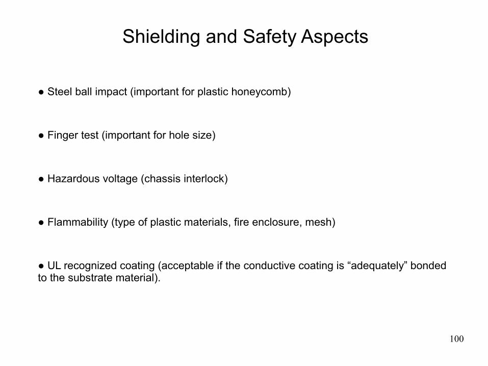
Shielding and Safety Aspects
● Steel ball impact (important for plastic honeycomb)
● Finger test (important for hole size)
● Hazardous voltage (chassis interlock)
● Flammability (type of plastic materials, fire enclosure, mesh)
● UL recognized coating (acceptable if the conductive coating is “adequately” bonded to the substrate material).

101
Thanks !
Sergiu Radu
EMC Design Engineering
Sun Microsystems, Inc.
(650) 786 3465


