Fabrication of Nanoscale BLM Biosensors
Tadahiro Kaburaki (Cornell)MR Burnham (Wadsworth Postdoc)
M.G. Spencer (Cornell PI)James Turner (Wadsworth PI)
Xinquin Jiang (Cornell)
Presentation Contents
• Objectives• Background• Fabricated devices• Signal Processing• Current Goals
Objectives
• Fabrication of a stable platform for transducing signals through artificial BLMs– Allow for the most stable BLM possible
• Analysis of BLM impedance characteristics– Including signals produced with proteins
• Packaging of a sensor with analytic capabilities on-chip
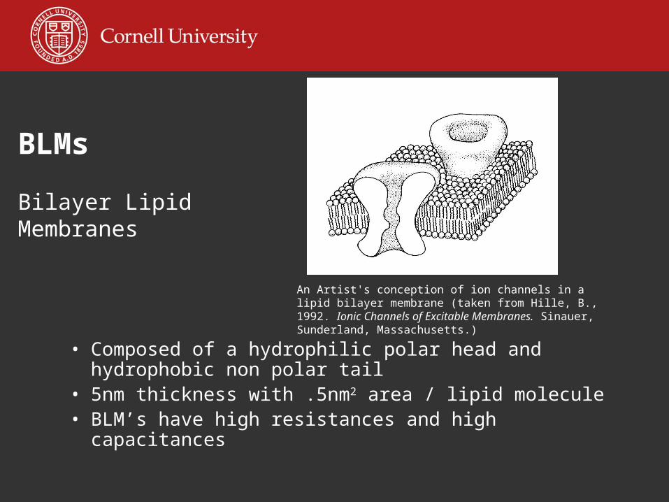
BLMs
• Composed of a hydrophilic polar head and hydrophobic non polar tail
• 5nm thickness with .5nm2 area / lipid molecule• BLM’s have high resistances and high capacitances
An Artist's conception of ion channels in a lipid bilayer membrane (taken from Hille, B., 1992. Ionic Channels of Excitable Membranes. Sinauer, Sunderland, Massachusetts.)
Bilayer Lipid Membranes
Why use a BLM/protein system?
• Biosensors based on natural receptors (proteins) with BLMs provide a sensitive and selective method of sensing chemical species (ions or molecules)
• Upon binding with analytes, transport proteins change their transport behavior across BLMs
• These types of sensors are unique in that they have molecular recognition as well as signal tranduction properties.
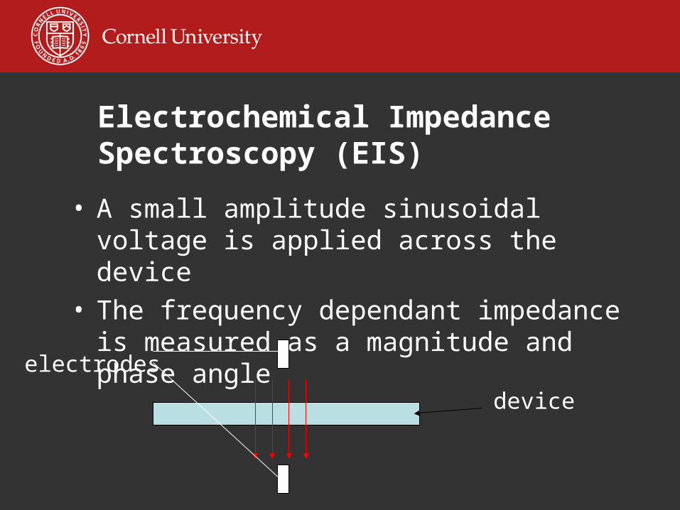
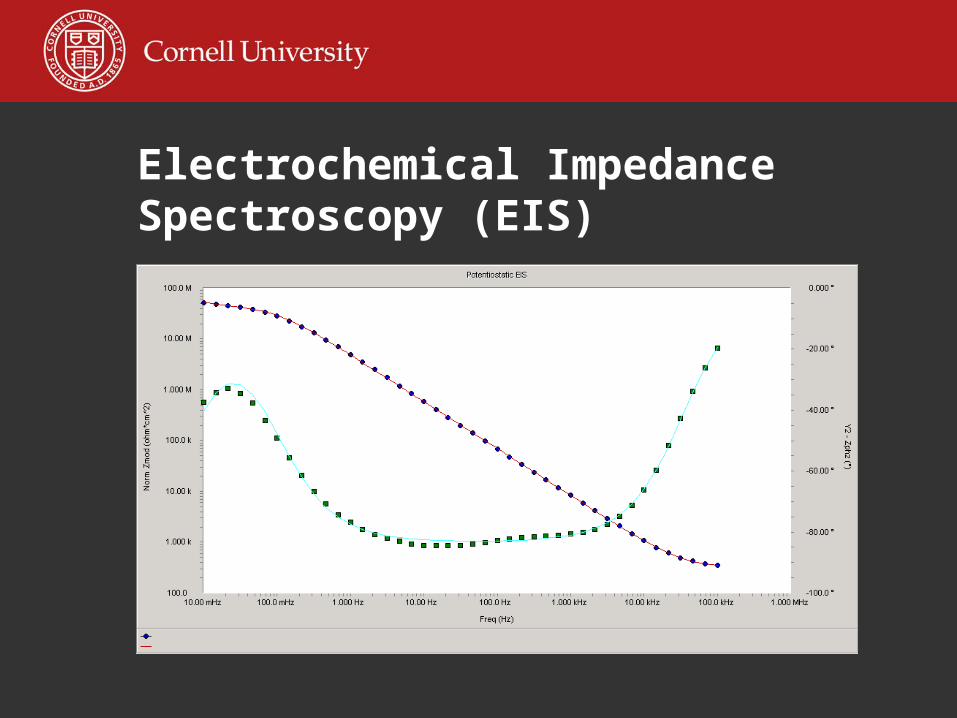
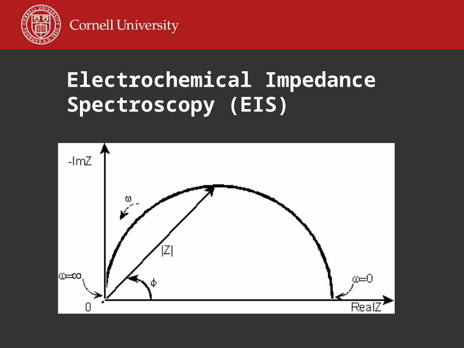
Electrochemical Impedance Spectroscopy (EIS)
• A small amplitude sinusoidal voltage is applied across the device
• The frequency dependant impedance is measured as a magnitude and phase angle
device
electrodes
Electrochemical Impedance Spectroscopy (EIS)
Electrochemical Impedance Spectroscopy (EIS)
Electrochemical Impedance Spectroscopy (EIS)
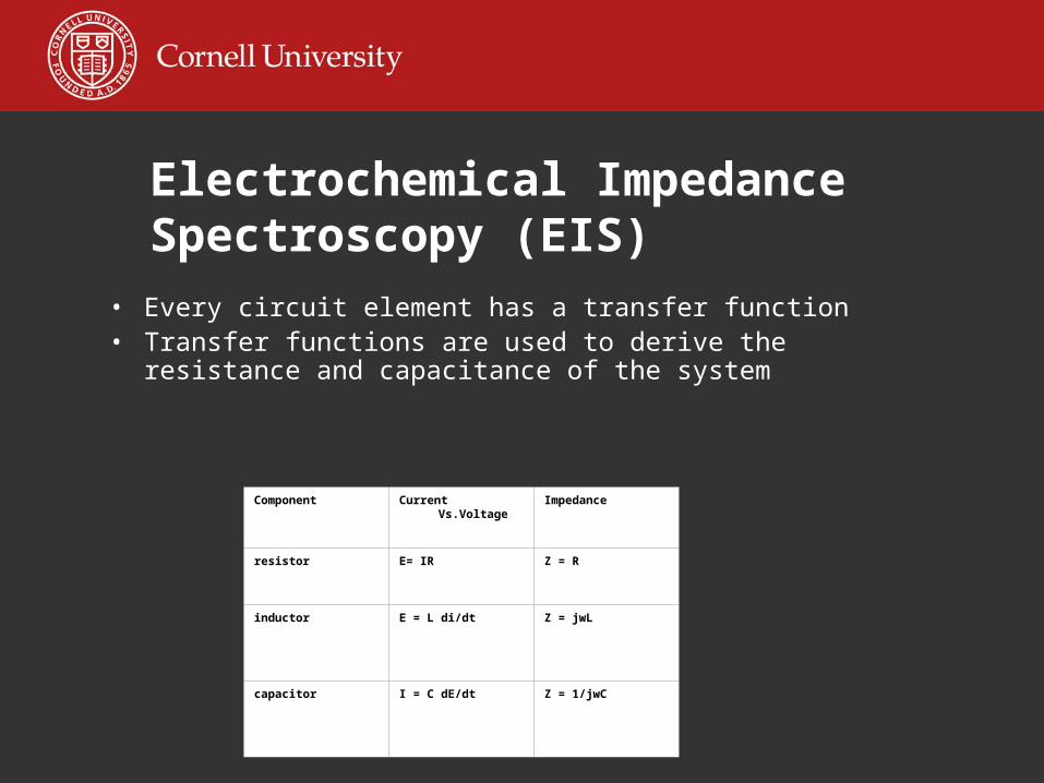
• Every circuit element has a transfer function• Transfer functions are used to derive the resistance and
capacitance of the system
Component Current Vs.Voltage
Impedance
resistor E= IR Z = R
inductor E = L di/dt Z = jwL
capacitor I = C dE/dt Z = 1/jwC
Electrochemical Impedance Spectroscopy (EIS)
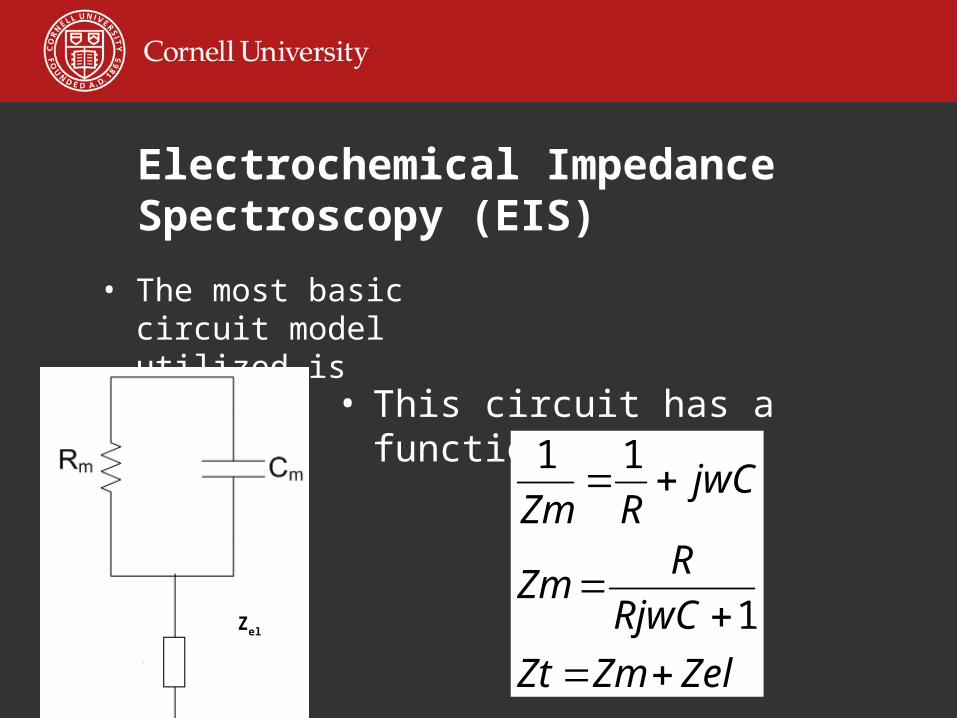
• The most basic circuit model utilized is
Zel
• This circuit has a function of
ZelZmZt
RjwC
RZm
jwCRZm
1
11
Electrochemical Impedance Spectroscopy (EIS)
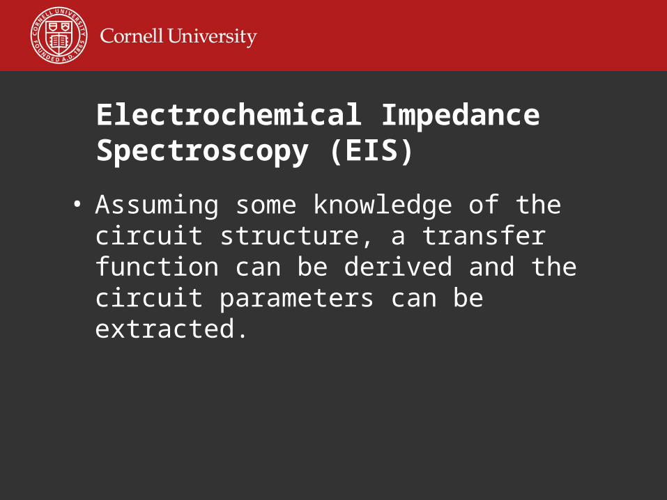
• Assuming some knowledge of the circuit structure, a transfer function can be derived and the circuit parameters can be extracted.
Electrochemical Impedance Spectroscopy (EIS)
• Unfortunately, these systems can be far more complicated due to a variety of other parasitic interactions– A primary source of these complications is the Si
substrate itself which is highly conductive. This presents a low conductance, high capacitance pathway when combined with the membrane.
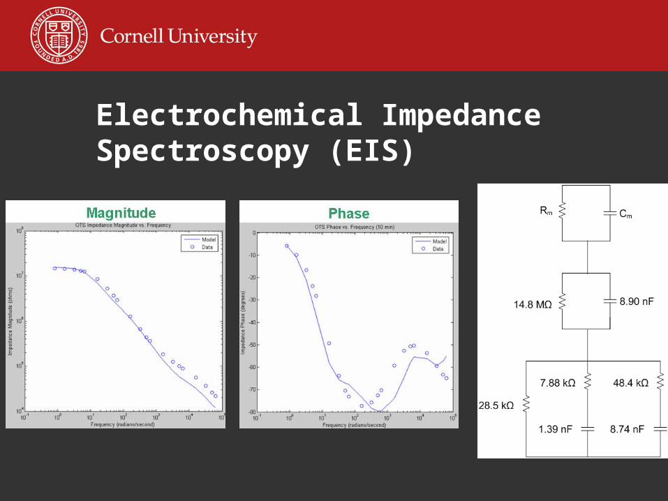
Electrochemical Impedance Spectroscopy (EIS)
•
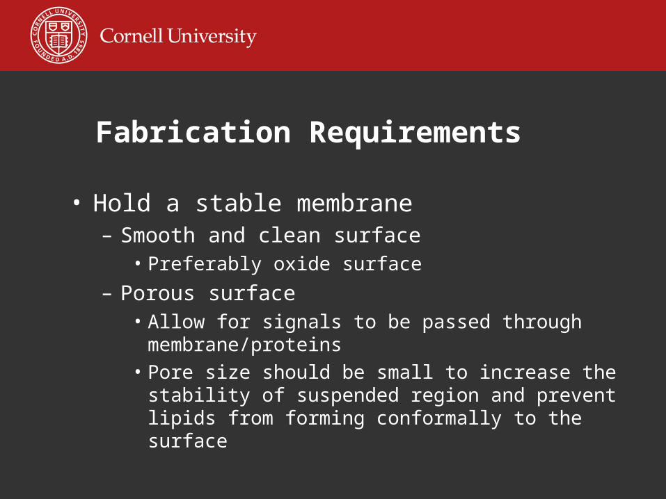
Fabrication Requirements
• Hold a stable membrane– Smooth and clean surface
• Preferably oxide surface
– Porous surface• Allow for signals to be passed through
membrane/proteins
• Pore size should be small to increase the stability of suspended region and prevent lipids from forming conformally to the surface

Fabrication Requirements
• Measure signals with a high S/N ratio– Need a high resistance, low capacitance substrate
• Prevents capacitive coupling, capacitive signal leakage
• High resistance allows for signals to be measured only through the membrane area
– Good electrode placement• i.e. Ag/AgCl electrodes for Cl- measurement

Porous alumina substrates
• Designed by Xinquin Jiang (Spencer group)– Utilizes porous alumina formed
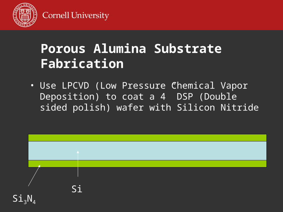
Porous Alumina Substrate Fabrication
• Use LPCVD (Low Pressure Chemical Vapor Deposition) to coat a 4” DSP (Double sided polish) wafer with Silicon Nitride
Si3N4
Si
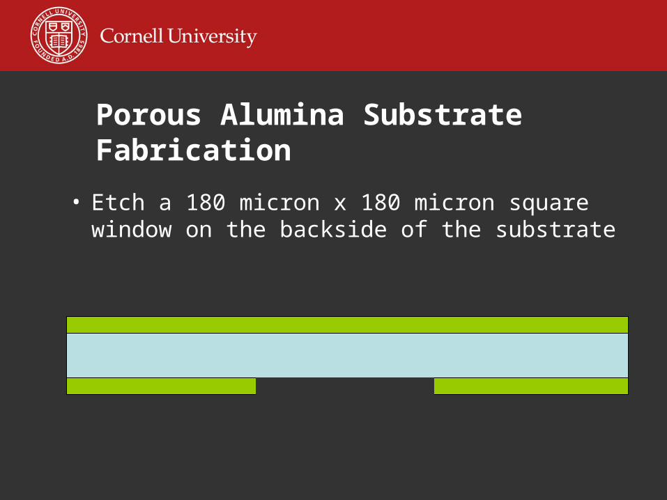
Porous Alumina Substrate Fabrication
• Etch a 180 micron x 180 micron square window on the backside of the substrate
Porous Alumina Substrate Fabrication
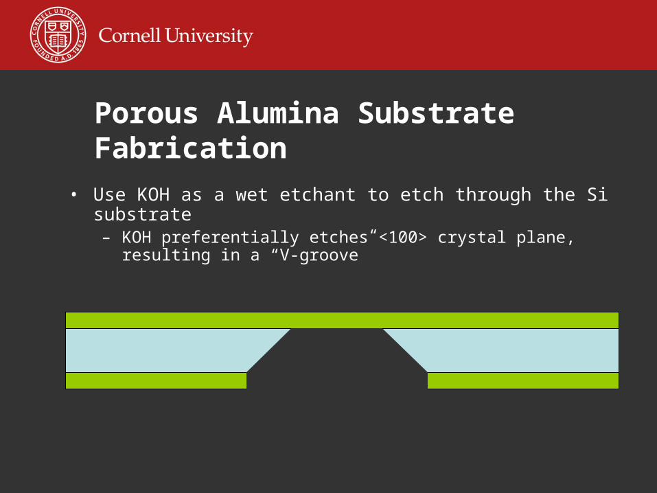
• Use KOH as a wet etchant to etch through the Si substrate– KOH preferentially etches <100> crystal plane, resulting in a “V-
groove”
Porous Alumina Substrate Fabrication
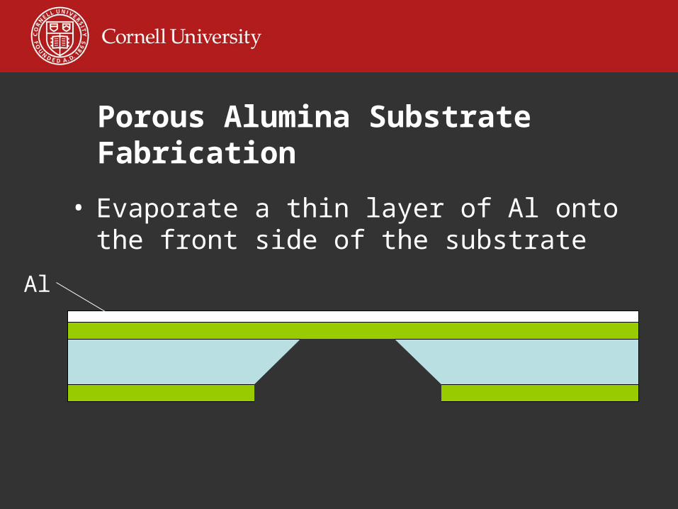
• Evaporate a thin layer of Al onto the front side of the substrate
Al
Porous Alumina Substrate Fabrication
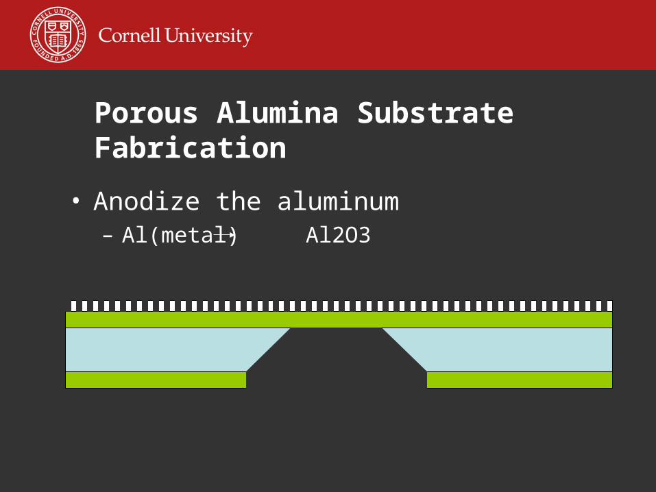
• Anodize the aluminum– Al(metal) Al2O3
Porous Alumina Substrate Fabrication
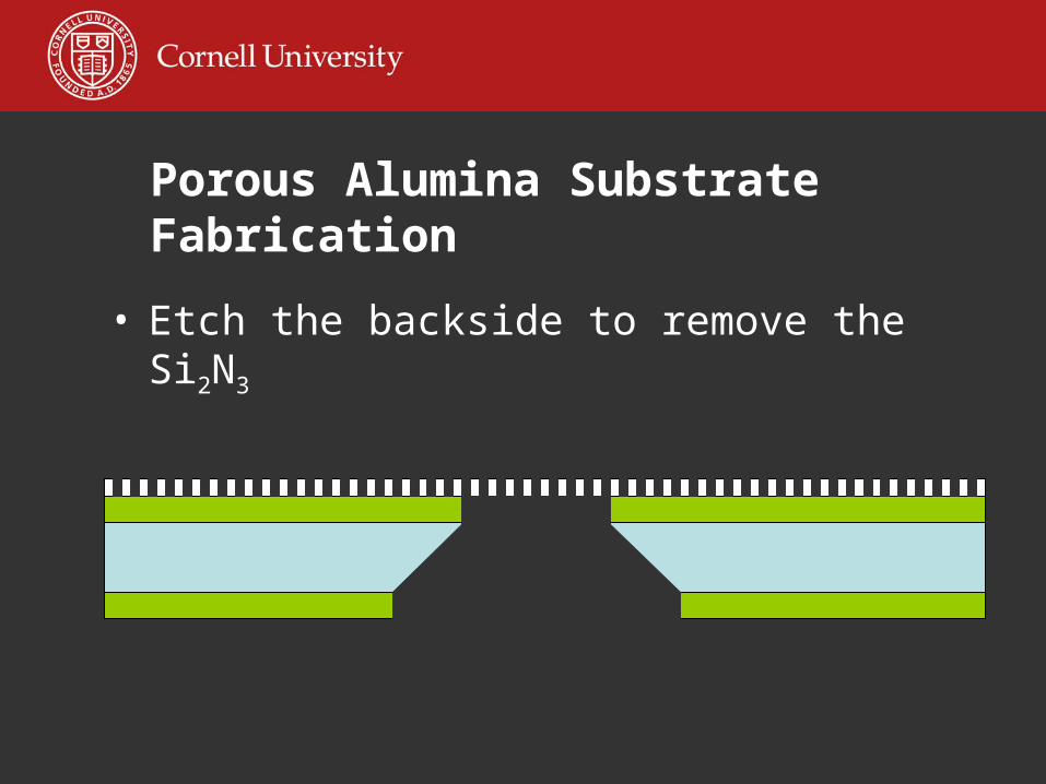
• Etch the backside to remove the Si2N3
Porous Alumina Substrate Fabrication
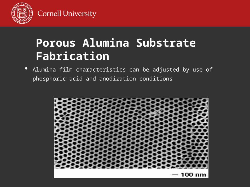
• Alumina film characteristics can be adjusted by use of phosphoric acid and
anodization conditions
Porous Alumina Substrate Fabrication
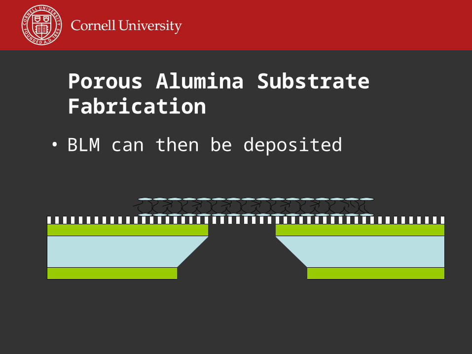
• BLM can then be deposited
Signals obtained from this system
• Our results are comparable to state of the art systems
• The results do require some amount of interpretation– This is because the systems on which the BLMs
reside are not identical.
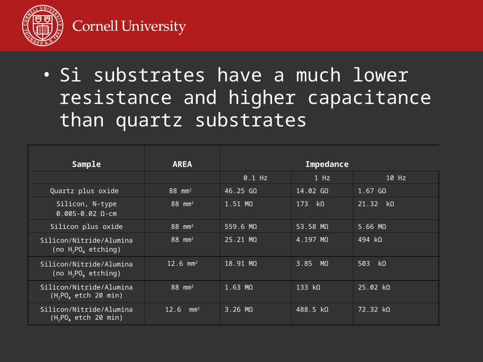
• Si substrates have a much lower resistance and higher capacitance than quartz substrates
Sample AREA Impedance
0.1 Hz 1 Hz 10 Hz
Quartz plus oxide 88 mm2 46.25 GΩ 14.02 GΩ 1.67 GΩ
Silicon, N-type
0.005-0.02 Ω-cm
88 mm2 1.51 MΩ 173 kΩ 21.32 kΩ
Silicon plus oxide 88 mm2 559.6 MΩ 53.58 MΩ 5.66 MΩ
Silicon/Nitride/Alumina (no H2PO4
etching)
88 mm2 25.21 MΩ 4.197 MΩ 494 kΩ
Silicon/Nitride/Alumina (no H2PO4
etching)
12.6 mm2 18.91 MΩ 3.85 MΩ 503 kΩ
Silicon/Nitride/Alumina (H2PO4 etch 20 min)
88 mm2 1.63 MΩ 133 kΩ 25.02 kΩ
Silicon/Nitride/Alumina (H2PO4 etch 20 min)
12.6 mm2 3.26 MΩ 488.5 kΩ 72.32 kΩ
Proposed Structure
• Change of Silicon substrate for SiO2
• Difficulty in etching through the wafer– HF wet etch is isotropic
– Dry etching of SiO2 has a maximum rate of 100nm/minute which is 5000 minutes for a 500um wafer.
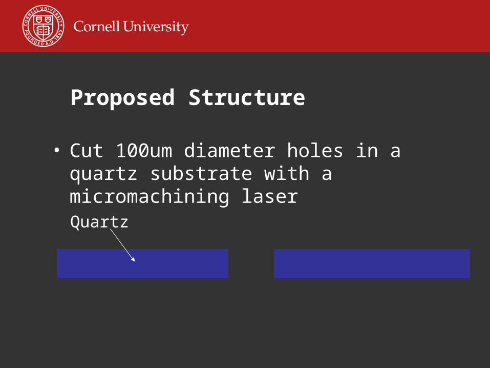
Proposed Structure
• Cut 100um diameter holes in a quartz substrate with a micromachining laser
Quartz
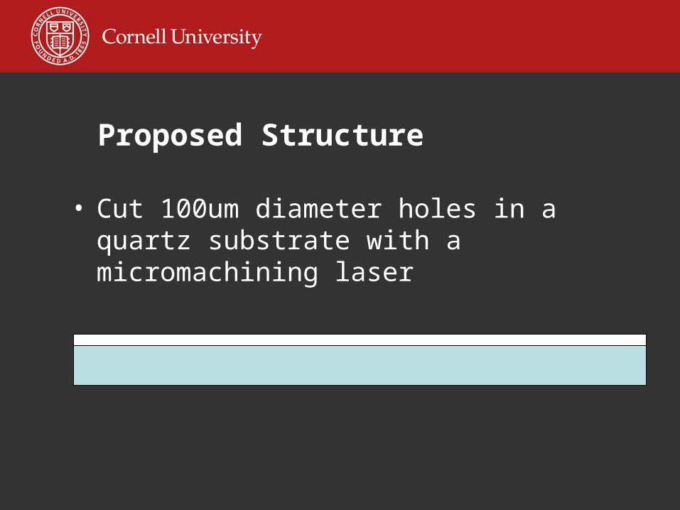
Proposed Structure
• Cut 100um diameter holes in a quartz substrate with a micromachining laser
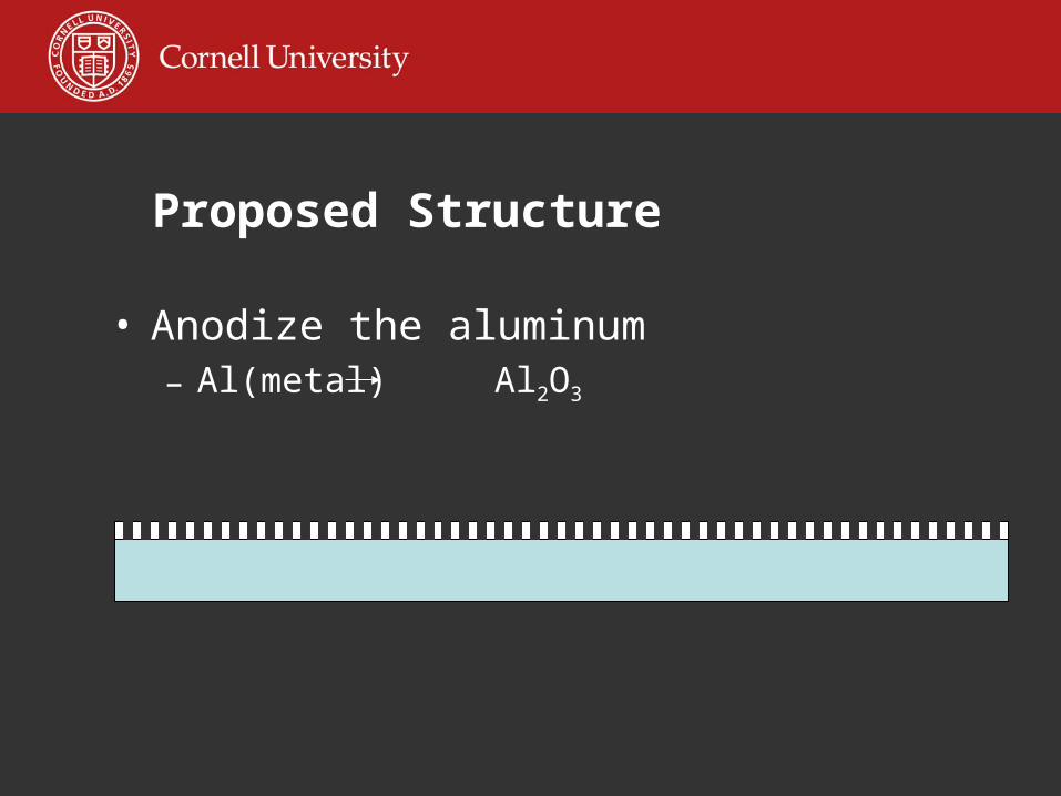
Proposed Structure
• Anodize the aluminum– Al(metal) Al2O3
Proposed Structure
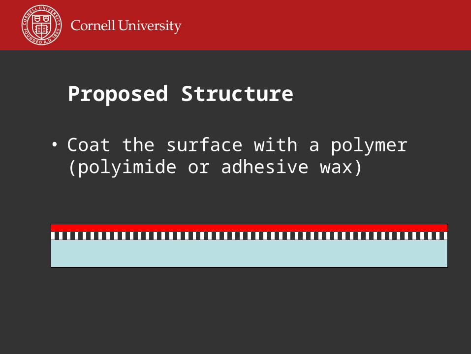
• Coat the surface with a polymer (polyimide or adhesive wax)
Proposed Structure
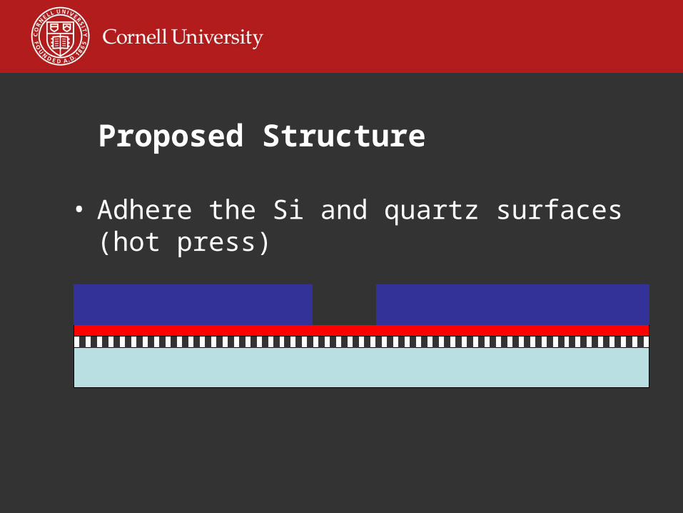
• Adhere the Si and quartz surfaces (hot press)
Proposed Structure
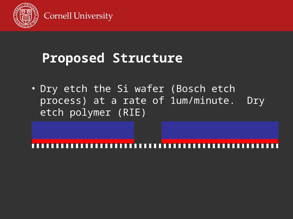
• Dry etch the Si wafer (Bosch etch process) at a rate of 1um/minute. Dry etch polymer (RIE)
Proposed Structure
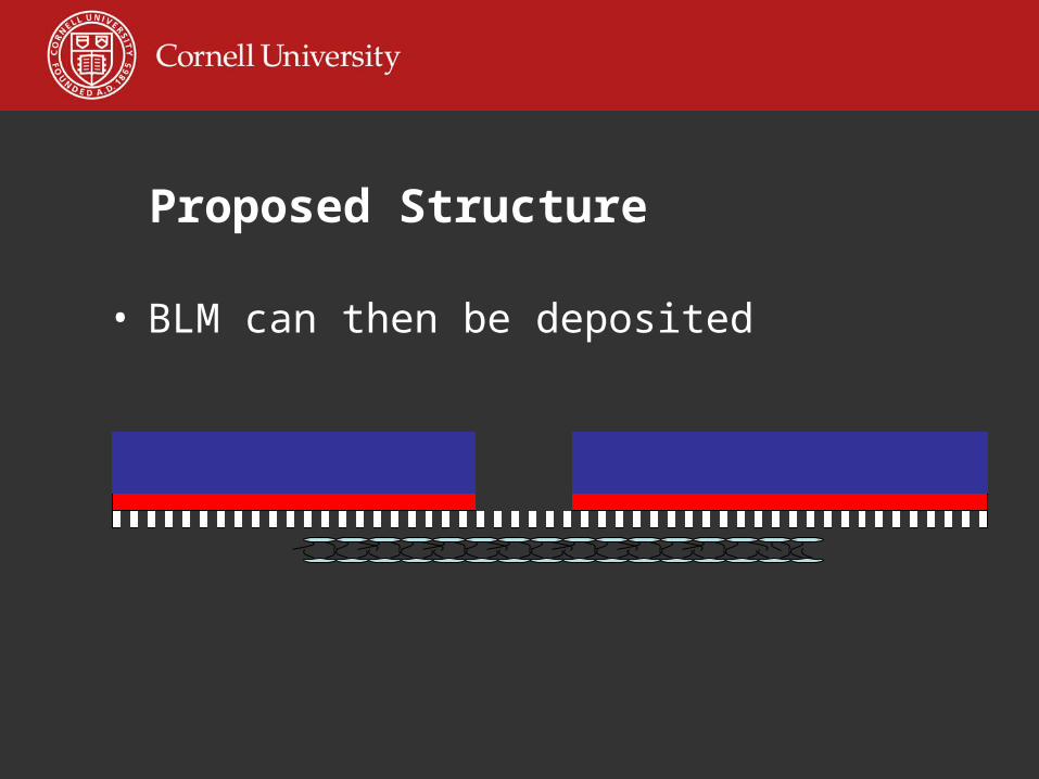
• BLM can then be deposited
The Next Step
• Addition of proteins– The proteins are the mechanism by which the
environment is actually measured– Measurements will be made at a single frequency
that is chosen to maximize sampling while remaining in the resistive regime
– Optimally this frequency will be in the kHz range

• Hirano from Nihon University used a patch clamp to measure current openings from a single gramicidin protein in response to different concentrations of ferritin avidin

• Opening percentage vs. FA concentration
Conclusion
• We have developed a system to hold membranes at a high resistance over a patterned substrate
• Current readings are feasible and should generate readable results due to the larger number of measurement proteins