fabrication of nanoscale blm biosensors tadahiro kaburaki (cornell) mr burnham (wadsworth postdoc)...
TRANSCRIPT
Fabrication of Nanoscale BLM Biosensors
Tadahiro Kaburaki (Cornell)MR Burnham (Wadsworth Postdoc)
M.G. Spencer (Cornell PI)James Turner (Wadsworth PI)
Xinquin Jiang (Cornell)
Presentation Contents
• Objectives• Background• Fabricated devices• Signal Processing• Current Goals
Objectives
• Fabrication of a stable platform for transducing signals through artificial BLMs– Allow for the most stable BLM possible
• Analysis of BLM impedance characteristics– Including signals produced with proteins
• Packaging of a sensor with analytic capabilities on-chip
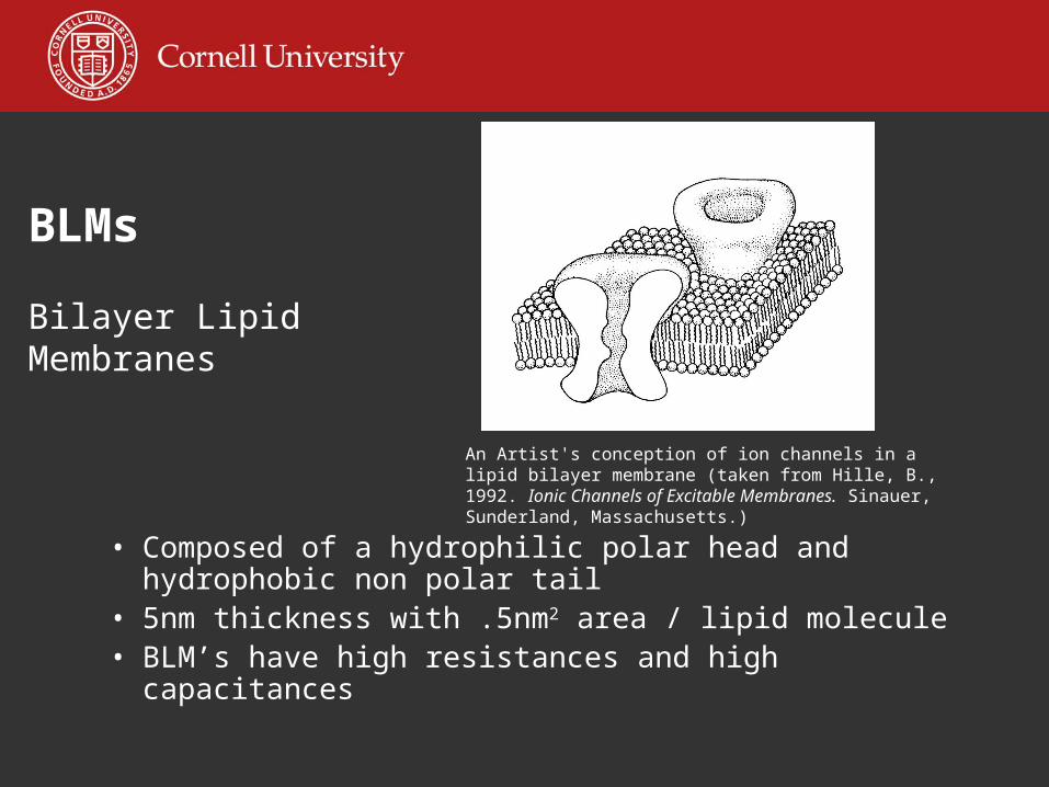
BLMs
• Composed of a hydrophilic polar head and hydrophobic non polar tail
• 5nm thickness with .5nm2 area / lipid molecule• BLM’s have high resistances and high capacitances
An Artist's conception of ion channels in a lipid bilayer membrane (taken from Hille, B., 1992. Ionic Channels of Excitable Membranes. Sinauer, Sunderland, Massachusetts.)
Bilayer Lipid Membranes
Why use a BLM/protein system?
• Biosensors based on natural receptors (proteins) with BLMs provide a sensitive and selective method of sensing chemical species (ions or molecules)
• Upon binding with analytes, transport proteins change their transport behavior across BLMs
• These types of sensors are unique in that they have molecular recognition as well as signal tranduction properties.
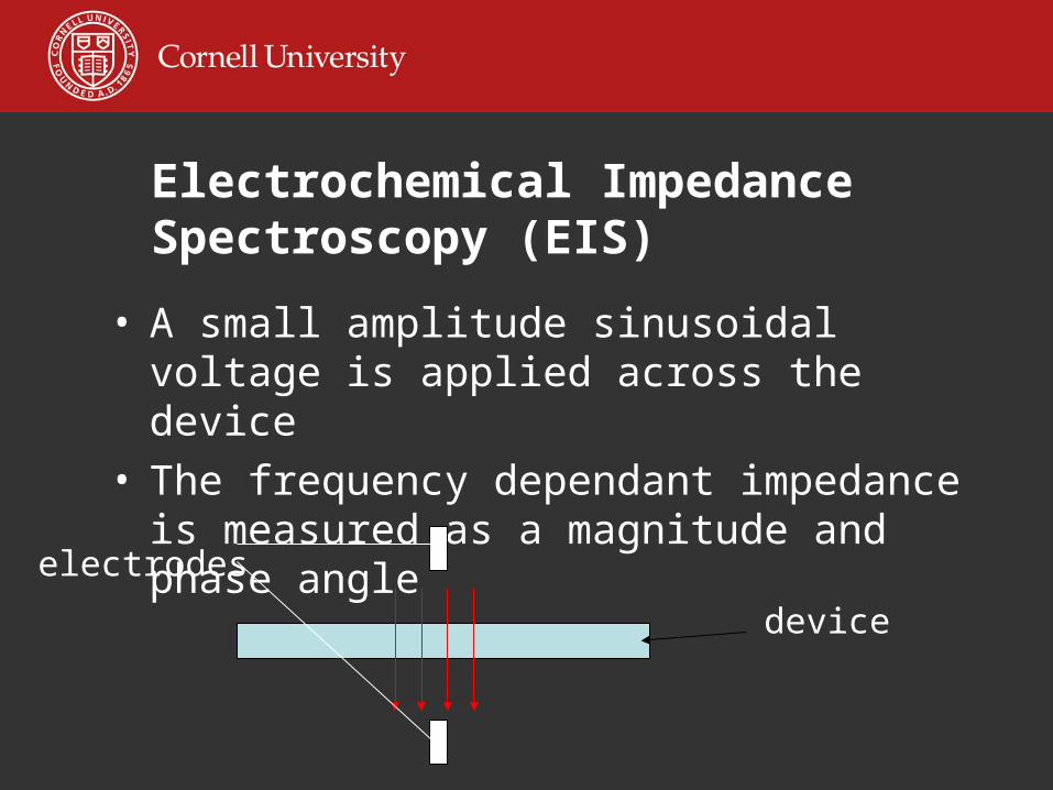
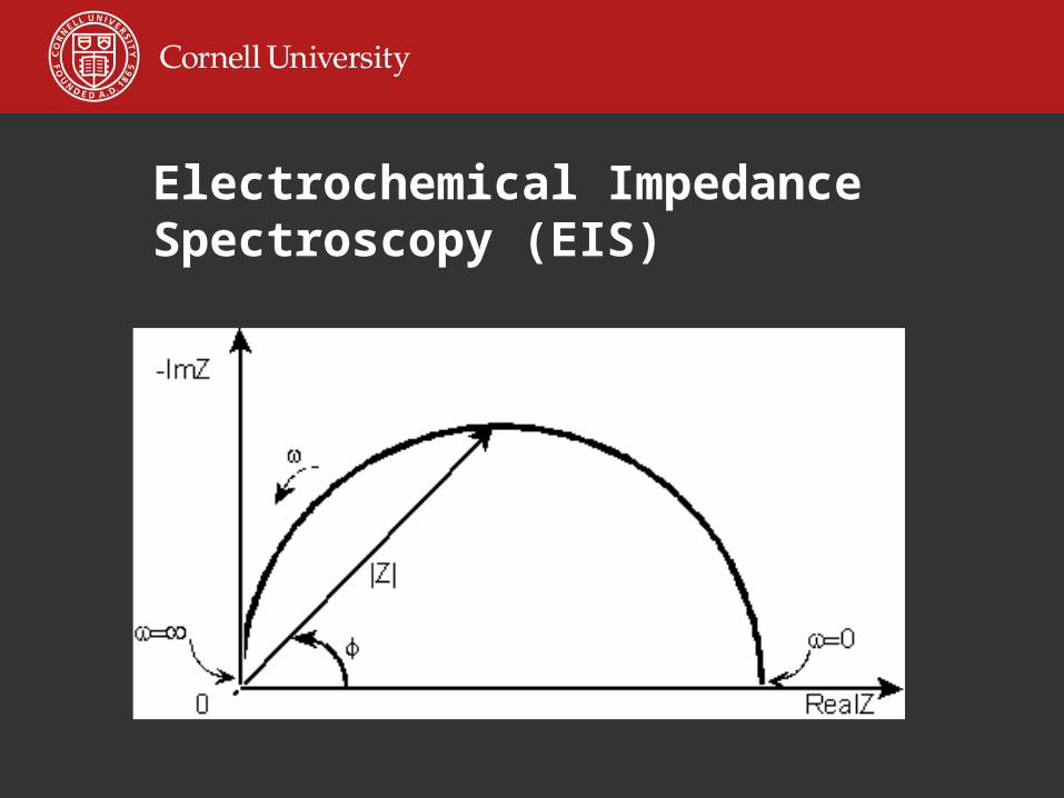
Electrochemical Impedance Spectroscopy (EIS)
• A small amplitude sinusoidal voltage is applied across the device
• The frequency dependant impedance is measured as a magnitude and phase angle
device
electrodes
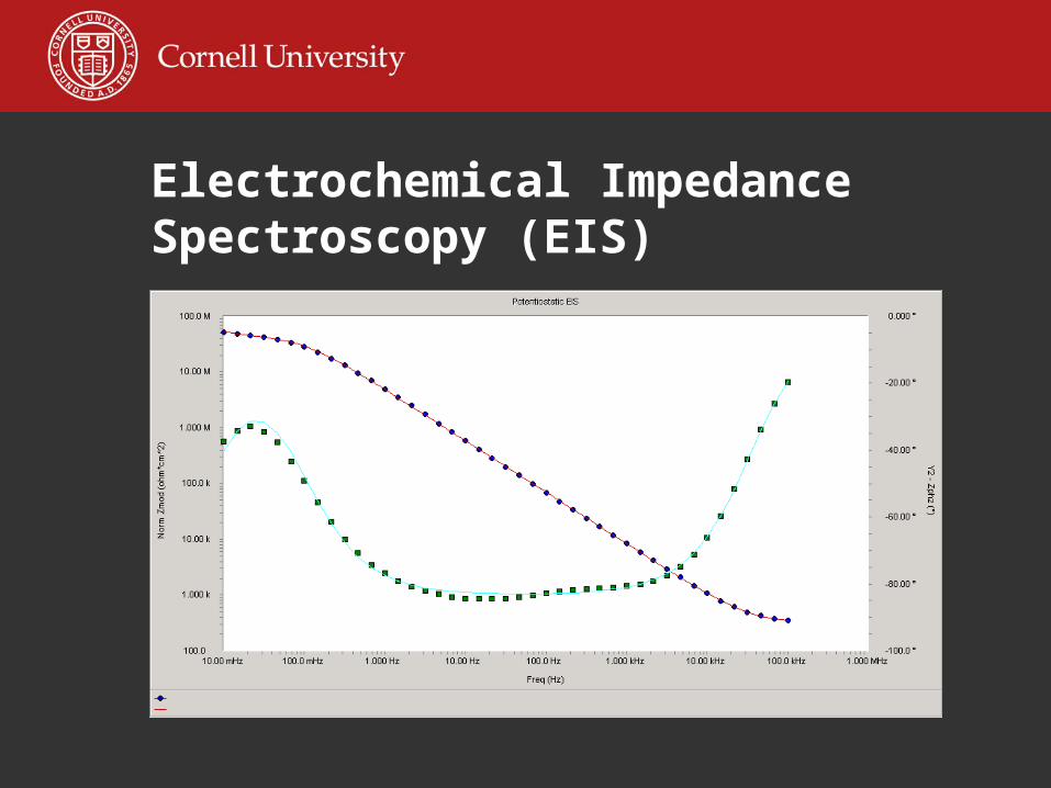
Electrochemical Impedance Spectroscopy (EIS)
Electrochemical Impedance Spectroscopy (EIS)
Electrochemical Impedance Spectroscopy (EIS)
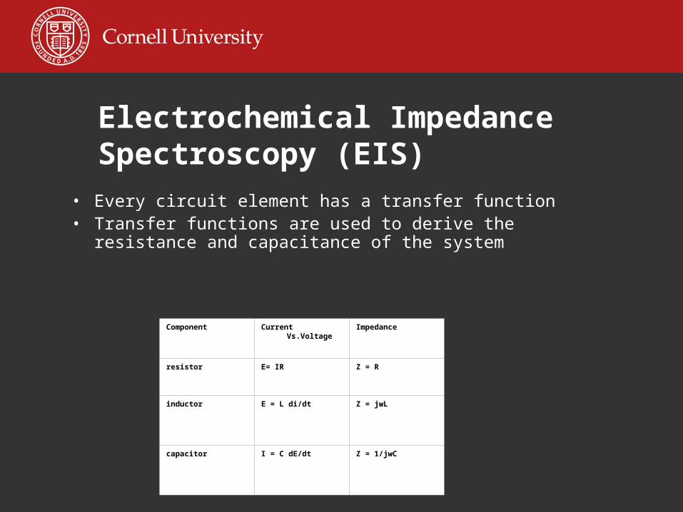
• Every circuit element has a transfer function• Transfer functions are used to derive the resistance and
capacitance of the system
Component Current Vs.Voltage
Impedance
resistor E= IR Z = R
inductor E = L di/dt Z = jwL
capacitor I = C dE/dt Z = 1/jwC
Electrochemical Impedance Spectroscopy (EIS)
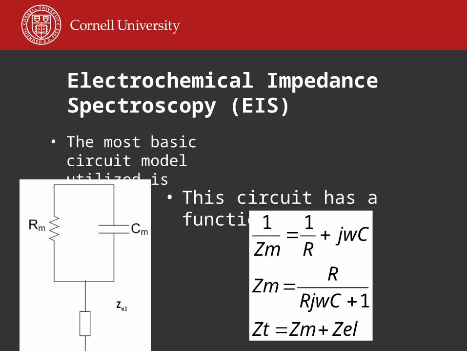
• The most basic circuit model utilized is
Zel
• This circuit has a function of
ZelZmZt
RjwC
RZm
jwCRZm
1
11
Electrochemical Impedance Spectroscopy (EIS)
• Assuming some knowledge of the circuit structure, a transfer function can be derived and the circuit parameters can be extracted.
Electrochemical Impedance Spectroscopy (EIS)
• Unfortunately, these systems can be far more complicated due to a variety of other parasitic interactions– A primary source of these complications is the Si
substrate itself which is highly conductive. This presents a low conductance, high capacitance pathway when combined with the membrane.
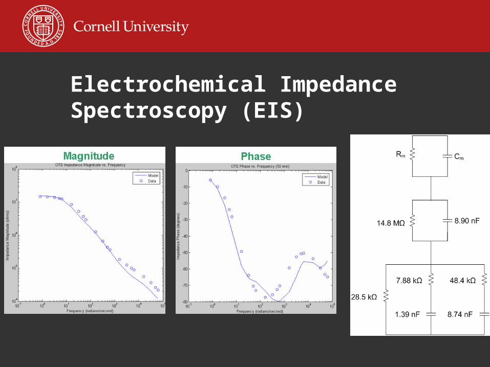
Electrochemical Impedance Spectroscopy (EIS)
•
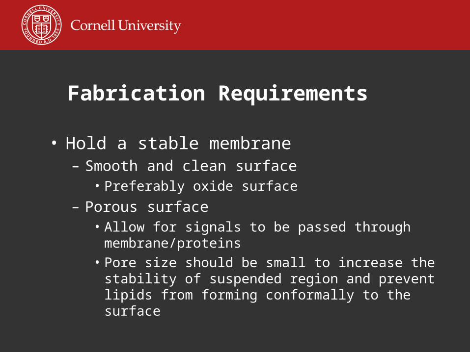
Fabrication Requirements
• Hold a stable membrane– Smooth and clean surface
• Preferably oxide surface
– Porous surface• Allow for signals to be passed through
membrane/proteins
• Pore size should be small to increase the stability of suspended region and prevent lipids from forming conformally to the surface

Fabrication Requirements
• Measure signals with a high S/N ratio– Need a high resistance, low capacitance substrate
• Prevents capacitive coupling, capacitive signal leakage
• High resistance allows for signals to be measured only through the membrane area
– Good electrode placement• i.e. Ag/AgCl electrodes for Cl- measurement

Porous alumina substrates
• Designed by Xinquin Jiang (Spencer group)– Utilizes porous alumina formed
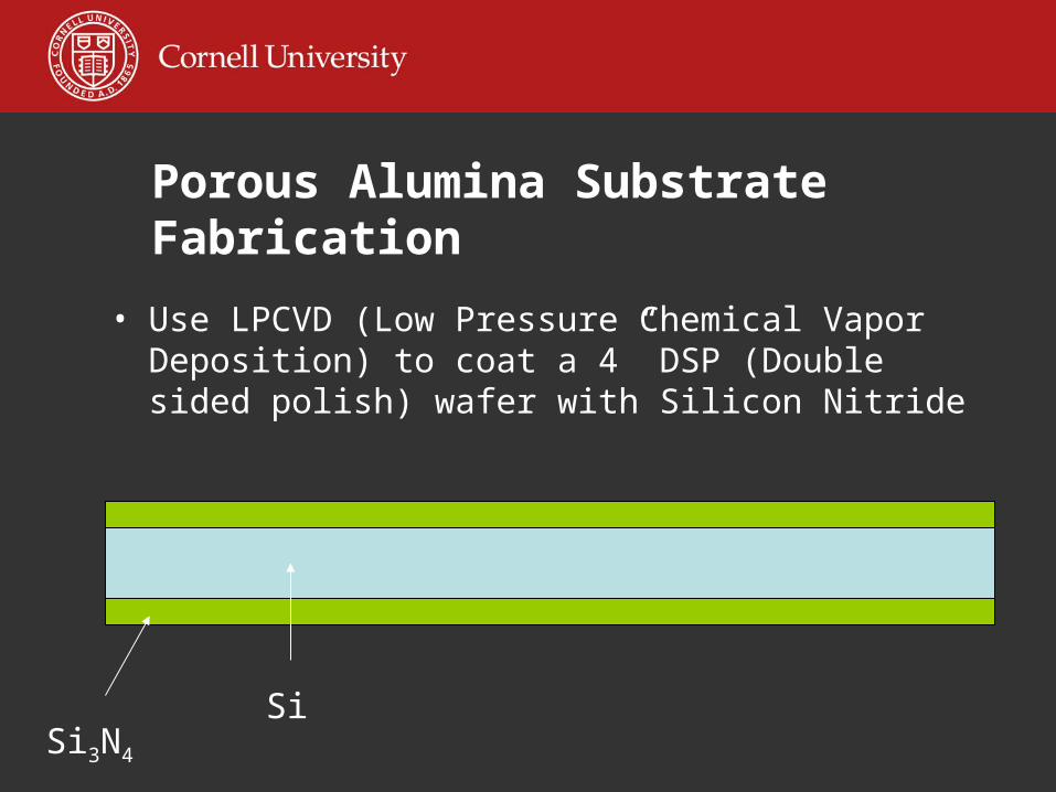
Porous Alumina Substrate Fabrication
• Use LPCVD (Low Pressure Chemical Vapor Deposition) to coat a 4” DSP (Double sided polish) wafer with Silicon Nitride
Si3N4
Si
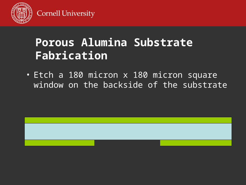
Porous Alumina Substrate Fabrication
• Etch a 180 micron x 180 micron square window on the backside of the substrate
Porous Alumina Substrate Fabrication
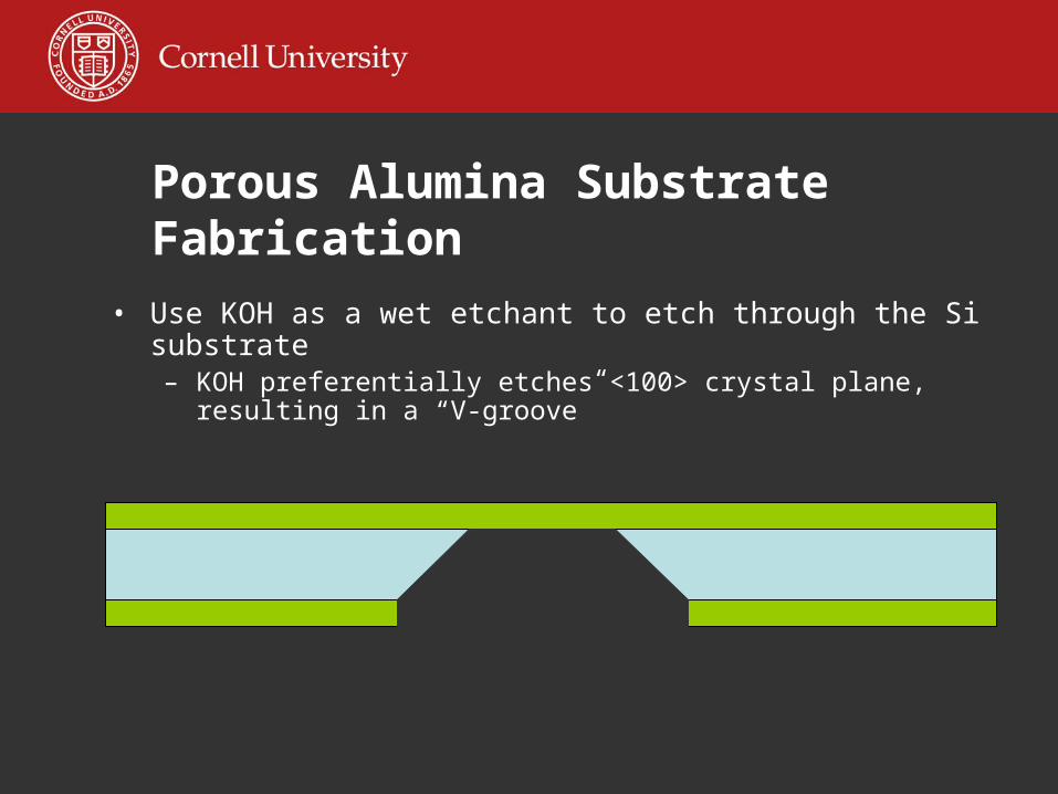
• Use KOH as a wet etchant to etch through the Si substrate– KOH preferentially etches <100> crystal plane, resulting in a “V-
groove”
Porous Alumina Substrate Fabrication
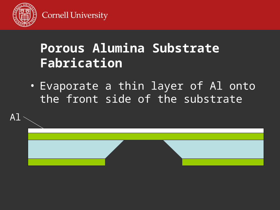
• Evaporate a thin layer of Al onto the front side of the substrate
Al
Porous Alumina Substrate Fabrication
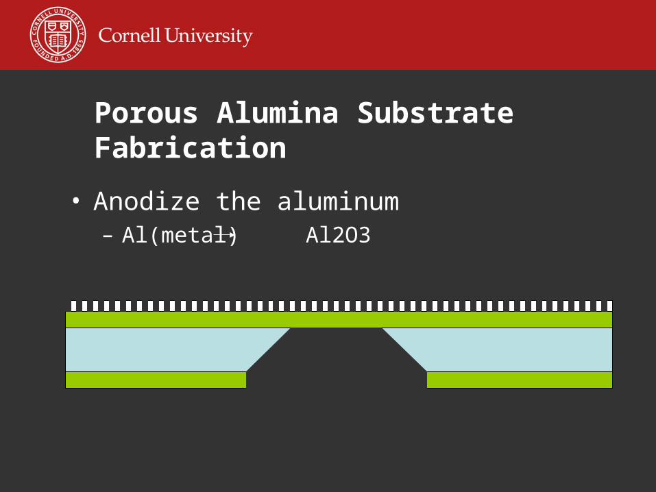
• Anodize the aluminum– Al(metal) Al2O3
Porous Alumina Substrate Fabrication
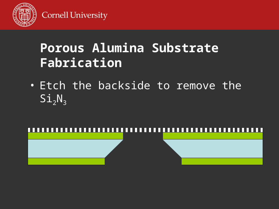
• Etch the backside to remove the Si2N3
Porous Alumina Substrate Fabrication
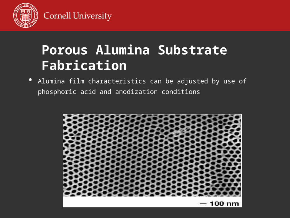
• Alumina film characteristics can be adjusted by use of phosphoric acid and
anodization conditions
Porous Alumina Substrate Fabrication
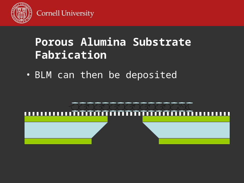
• BLM can then be deposited
Signals obtained from this system
• Our results are comparable to state of the art systems
• The results do require some amount of interpretation– This is because the systems on which the BLMs
reside are not identical.
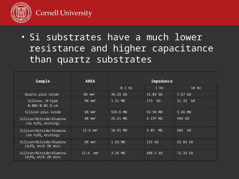
• Si substrates have a much lower resistance and higher capacitance than quartz substrates
Sample AREA Impedance
0.1 Hz 1 Hz 10 Hz
Quartz plus oxide 88 mm2 46.25 GΩ 14.02 GΩ 1.67 GΩ
Silicon, N-type
0.005-0.02 Ω-cm
88 mm2 1.51 MΩ 173 kΩ 21.32 kΩ
Silicon plus oxide 88 mm2 559.6 MΩ 53.58 MΩ 5.66 MΩ
Silicon/Nitride/Alumina (no H2PO4
etching)
88 mm2 25.21 MΩ 4.197 MΩ 494 kΩ
Silicon/Nitride/Alumina (no H2PO4
etching)
12.6 mm2 18.91 MΩ 3.85 MΩ 503 kΩ
Silicon/Nitride/Alumina (H2PO4 etch 20 min)
88 mm2 1.63 MΩ 133 kΩ 25.02 kΩ
Silicon/Nitride/Alumina (H2PO4 etch 20 min)
12.6 mm2 3.26 MΩ 488.5 kΩ 72.32 kΩ
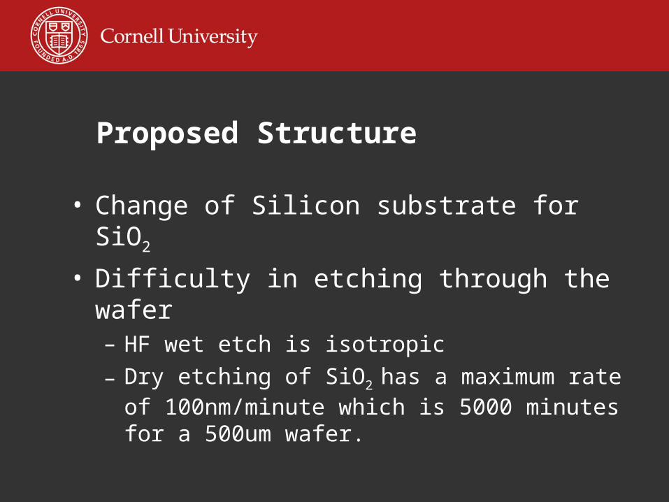
Proposed Structure
• Change of Silicon substrate for SiO2
• Difficulty in etching through the wafer– HF wet etch is isotropic
– Dry etching of SiO2 has a maximum rate of 100nm/minute which is 5000 minutes for a 500um wafer.
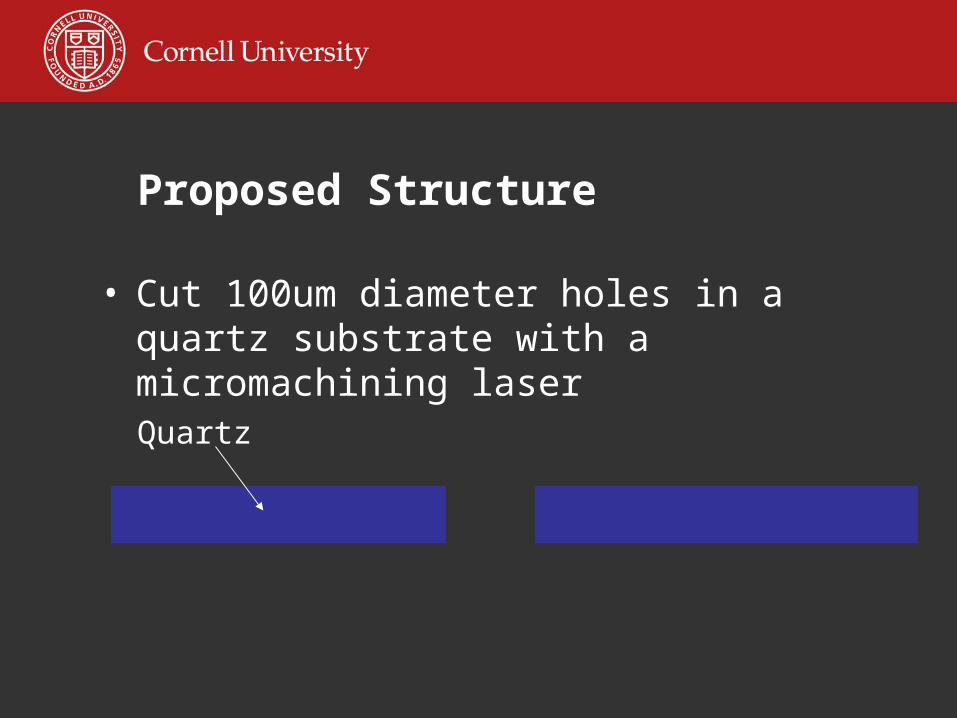
Proposed Structure
• Cut 100um diameter holes in a quartz substrate with a micromachining laser
Quartz
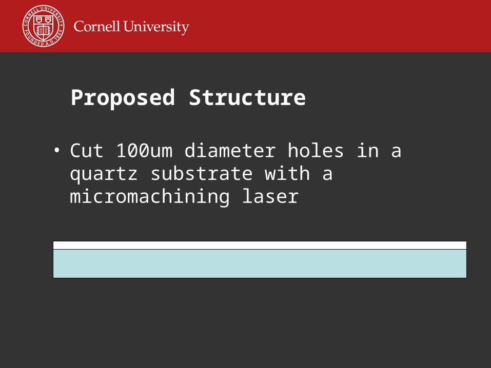
Proposed Structure
• Cut 100um diameter holes in a quartz substrate with a micromachining laser
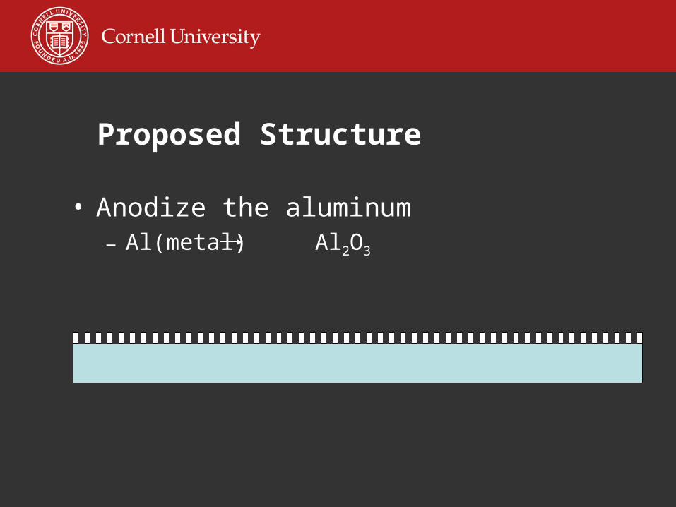
Proposed Structure
• Anodize the aluminum– Al(metal) Al2O3
Proposed Structure
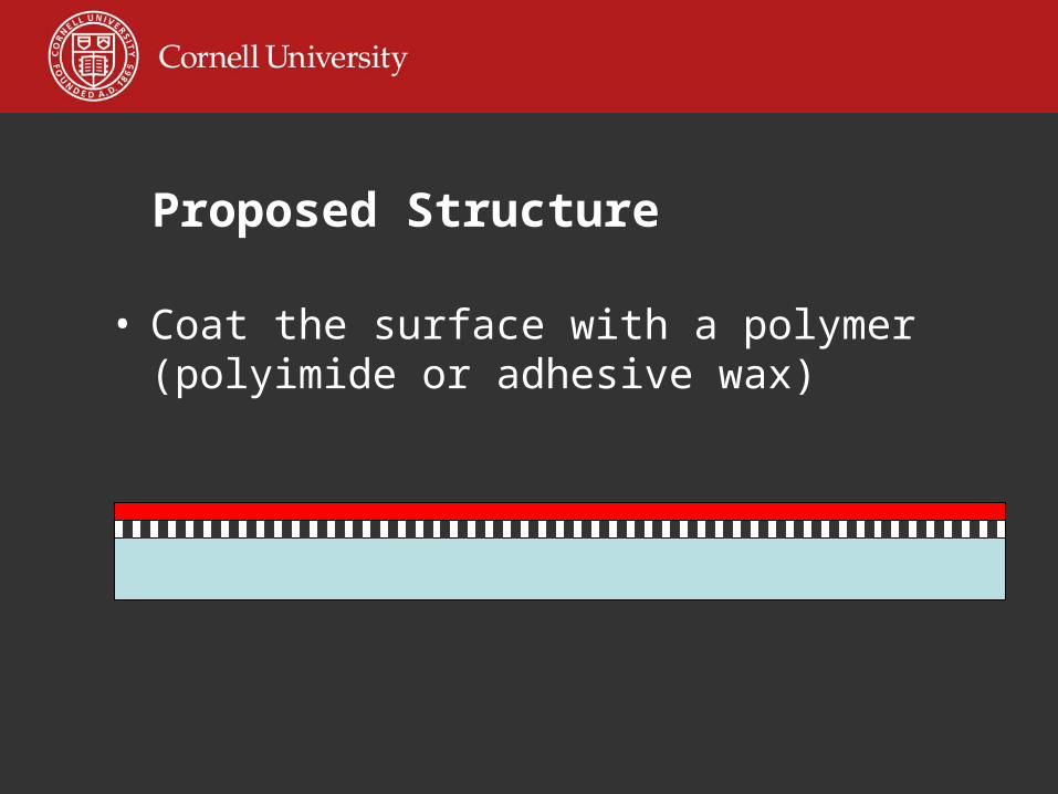
• Coat the surface with a polymer (polyimide or adhesive wax)
Proposed Structure
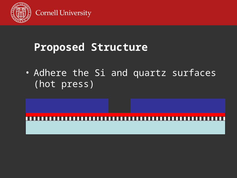
• Adhere the Si and quartz surfaces (hot press)
Proposed Structure
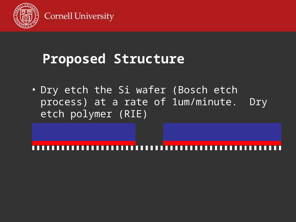
• Dry etch the Si wafer (Bosch etch process) at a rate of 1um/minute. Dry etch polymer (RIE)
Proposed Structure
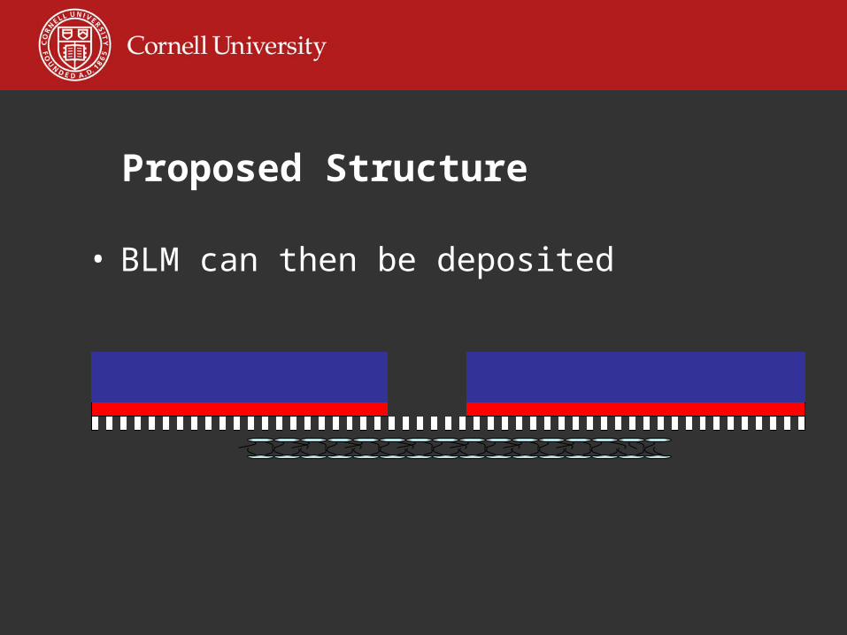
• BLM can then be deposited
The Next Step
• Addition of proteins– The proteins are the mechanism by which the
environment is actually measured– Measurements will be made at a single frequency
that is chosen to maximize sampling while remaining in the resistive regime
– Optimally this frequency will be in the kHz range

• Hirano from Nihon University used a patch clamp to measure current openings from a single gramicidin protein in response to different concentrations of ferritin avidin

• Opening percentage vs. FA concentration
Conclusion
• We have developed a system to hold membranes at a high resistance over a patterned substrate
• Current readings are feasible and should generate readable results due to the larger number of measurement proteins