
Toward an Advanced Intelligent Memory
System
University of Illinois
Y. Kang, W. Huang, S. Yoo, D. KeenZ. Ge, V. Lam, P. Pattnaik, J. Torrellas
http://iacoma.cs.uiuc.edu
FlexRAM

Rationale
Large & increasing speed gap bottleneck for many apps.
Latency hiding bandwidth regaining techniques: diminishing returns out of order lockup free large cache, deep hierarchies
P/M integration: latency, bandwidth

Technological Landscape
Merged Logic and DRAM (MLD): IBM, Mitsubishi, Samsung, Toshiba and others
Powerful: e.g. IBM SA-27E ASIC (Feb 99) 0.18 m (chips for 1 Gbit DRAM) Logic frequency: 400 MHz IBM PowerPC 603 proc + 16 KB I, D caches =
3% Further advances in the horizon
Opportunity: How to exploit MLD best?
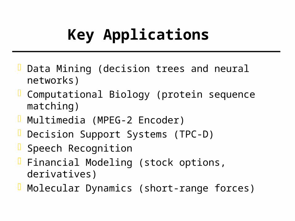
Key Applications
Data Mining (decision trees and neural networks)
Computational Biology (protein sequence matching)
Multimedia (MPEG-2 Encoder) Decision Support Systems (TPC-D)Speech RecognitionFinancial Modeling (stock options, derivatives)Molecular Dynamics (short-range forces)

Example App: Protein Matching
Problem: Find areas of database protein chains that match (modulo some mutations) the sample protein chains

How the Algorithm Works
Generate most-likely mutations
Pick 4 consecutive amino acids from sample
GDSL
GDSI GDSM
ADSI AESI
AETI GETM

Example App: Protein Matching
If match is found: try to extend it
Compare them to every positions in the database proteins

How to Use MLD
Main compute engine of the machine Add a traditional processor to DRAM chip
Incremental gains Include a special (vector/multi) processor Hard to
program
UC Berkeley: IRAMNotre Dame: Execube, PetaflopsMIT: RawStanford: Smart Memories

How to Use MLD (II)
Co-processor, special-purpose processor ATM switch controller Process data beside the disk Graphics accelerator
Stanford: ImagineUC Berkeley: ISTORE

How to Use MLD (III)
Our approach: replace memory chips PIM chip processes the memory-intensive parts
of the program
Illinois: FlexRAMUC Davis: Active PagesUSC-ISI: DIVA
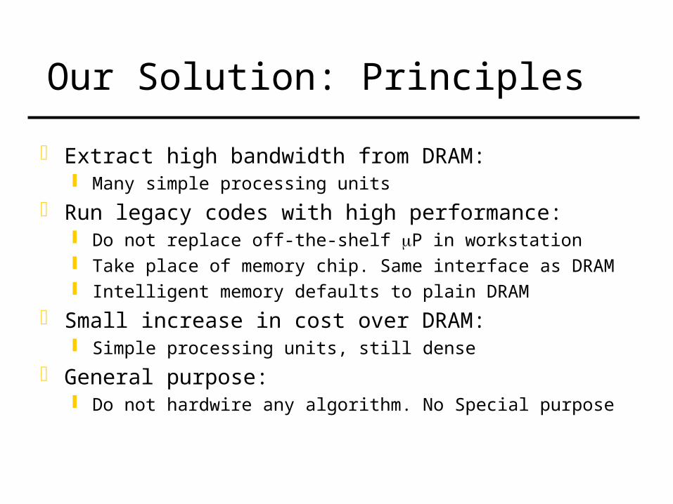
Our Solution: Principles
Extract high bandwidth from DRAM: Many simple processing units
Run legacy codes with high performance: Do not replace off-the-shelf P in workstation Take place of memory chip. Same interface as DRAM Intelligent memory defaults to plain DRAM
Small increase in cost over DRAM: Simple processing units, still dense
General purpose: Do not hardwire any algorithm. No Special purpose

Architecture Proposed

Chip Organization
•Organized in 64 1-Mbyte banks
•Each bank:
•Associated to 1 P.Array
•1 single port
•2 row buffers (2KB)
•P.Array access: 10ns (RB hit) 20ns (miss)
•On-chip memory b/w 102GB/s
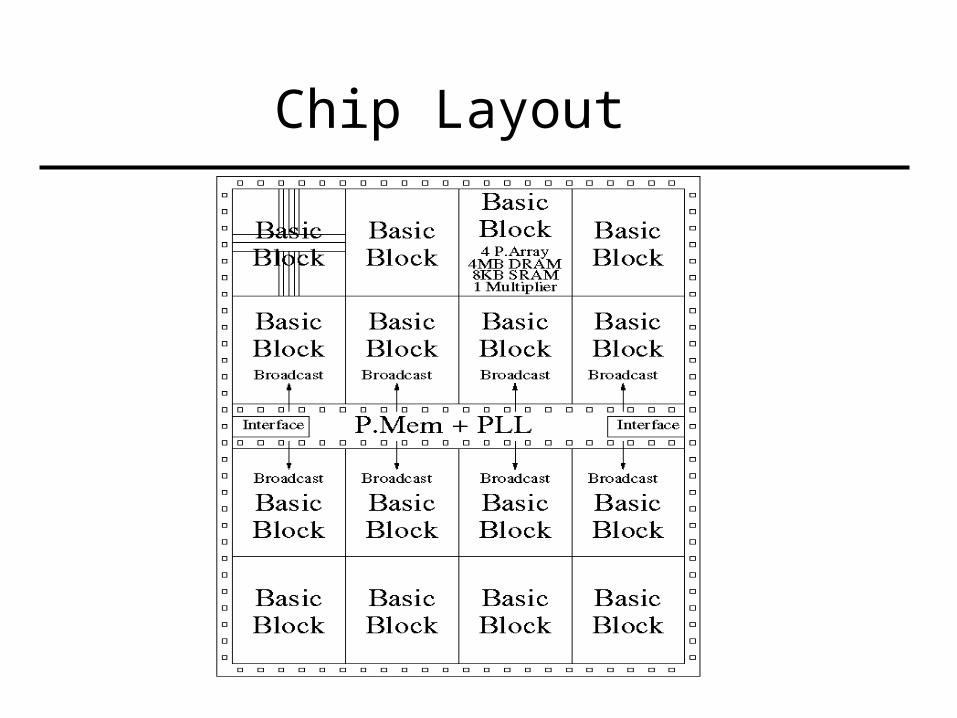
Chip Layout

Basic Block
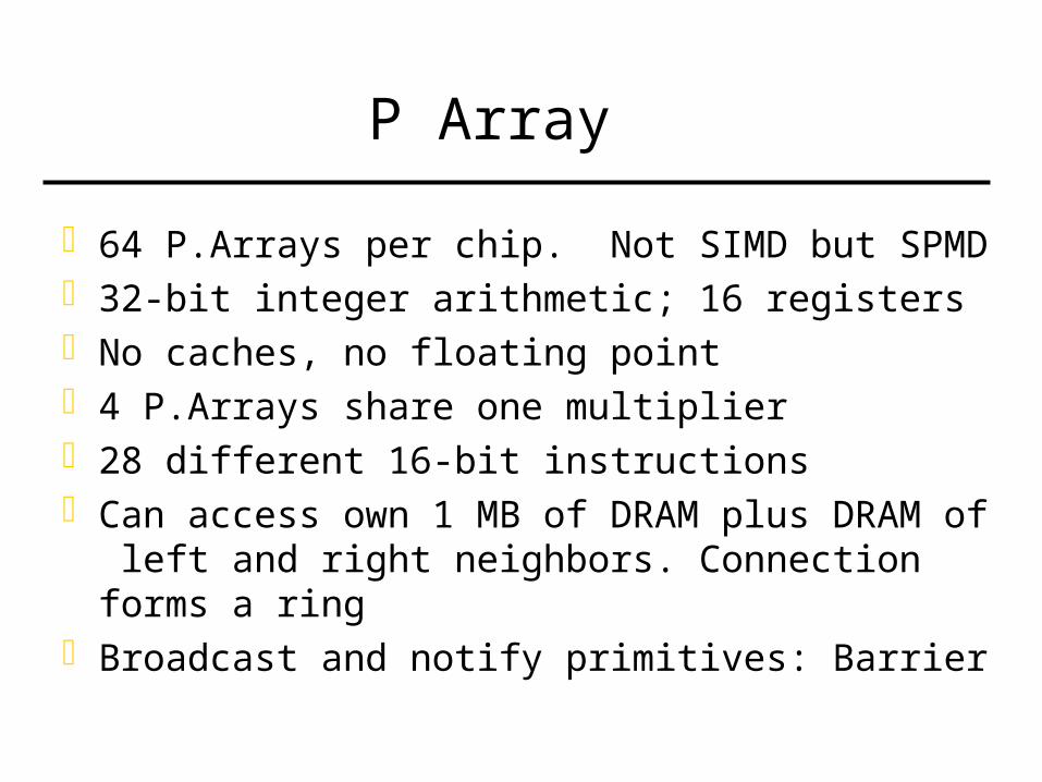
P Array
64 P.Arrays per chip. Not SIMD but SPMD32-bit integer arithmetic; 16 registersNo caches, no floating point4 P.Arrays share one multiplier28 different 16-bit instructionsCan access own 1 MB of DRAM plus DRAM of
left and right neighbors. Connection forms a ring
Broadcast and notify primitives: Barrier

Instruction Memory
Group of 4 P.Arrays share one 8-Kbyte, 4-ported SRAM instruction memory (not I-cache) Holds the P.Array code Small because short code Aggressive access time: 1 cycle = 2.5 ns

P Mem
2-issue in-order: PowerPC 603 16KB I,D caches
Executes serial sectionsCommunication with P.Arrays:
Broadcast/notify or plain write/read to memory Communication with other P.Mems:
Memory in all chips is visibleAccess via the inter-chip networkMust flush caches to ensure data coherence

Area Estimation (mm )
PowerPC 603+caches: 12
SRAM instruction memory: 34
64 Mbytes of DRAM: 330
P.Arrays: 96
Pads + network interf. + refresh logic 20
Rambus interface: 3.4Multipliers: 10
Total = 505
Of which 28% logic, 65% DRAM, 7% SRAM
2
Issues
Communication P.Mem-P.Host: P.Mem cannot be the master of bus Protocol intensive interface: Rambus
Virtual memory: P.Mems and P.Arrays use virtual addresses Small TLB for P.Arrays Special page mapping

EvaluationP.Host P.Host L1 & L2 Bus & Memory Freq: 800 MHz L1 Size: 32 KB Bus: Split Trans Issue Width: 6 L1 RT: 2.5 ns Bus Width: 16 B Dyn Issue: Yes L1 Assoc: 2 Bus Freq: 100 MHz I-Window Size: 96 L1 Line: 64 B Mem RT: 262.5 ns Ld/St Units: 2 L2 Size: 256 KB Int Units: 6 L2 RT: 12.5 ns FP Units: 4 L2 Assoc: 4 Pending Ld/St: 8/8 L2 Line: 64 B BR Penalty: 4 cyc P.Mem P.Mem L1 P.Array Freq: 400 MHz L1 Size: 16 KB Freq: 400 MHz Issue Width: 2 L1 RT: 2.5 ns Issue Width: 1 Dyn Issue: No L1 Assoc: 2 Dyn Issue: No Ld/St Units: 2 L1 Line: 32 B Pending St: 1 Int Units: 2 L2 Cache: No Row Buffers: 3 FP Units: 2 RB Size: 2 KB Pending Ld/St: 8/8 RB Hit: 10 ns BR Penalty: 2 cyc RB Miss: 20 ns

Speedups
Constant Problem Size Scaled Problem Size

Utilization
Low P.Host Utilization

Utilization
High P.Array Utilization Low P.Mem Utilization

Speedups
Varying Logic Frequency

Problems & Future Work
Fabrication technology heat, power dissipation, effect of logic noise on memory, package, yield, cost
Fault tolerance defect memory bank, processor
Compiler, Programming Language.

Conclusion
We have a handle on: A promising technology (MLD) Key applications of industrial interest
Real chance to transform the computing landscape
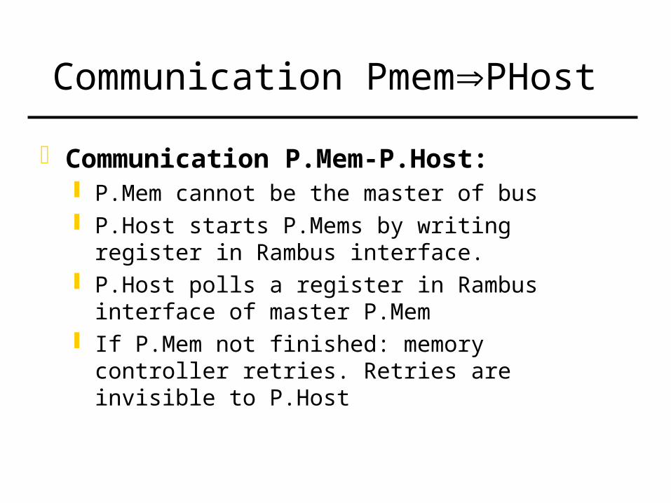
Communication PmemPHost
Communication P.Mem-P.Host: P.Mem cannot be the master of bus P.Host starts P.Mems by writing register in
Rambus interface. P.Host polls a register in Rambus interface of
master P.Mem If P.Mem not finished: memory controller
retries. Retries are invisible to P.Host

Virtual Address Translation


