toward an advanced intelligent memory system university of illinois y. kang, w. huang, s. yoo, d....
TRANSCRIPT

Toward an Advanced Intelligent Memory
System
University of Illinois
Y. Kang, W. Huang, S. Yoo, D. KeenZ. Ge, V. Lam, P. Pattnaik, J. Torrellas
http://iacoma.cs.uiuc.edu
FlexRAM

Rationale
Large & increasing speed gap bottleneck for many apps.
Latency hiding bandwidth regaining techniques: diminishing returns out of order lockup free large cache, deep hierarchies
P/M integration: latency, bandwidth

Technological Landscape
Merged Logic and DRAM (MLD): IBM, Mitsubishi, Samsung, Toshiba and others
Powerful: e.g. IBM SA-27E ASIC (Feb 99) 0.18 m (chips for 1 Gbit DRAM) Logic frequency: 400 MHz IBM PowerPC 603 proc + 16 KB I, D caches =
3% Further advances in the horizon
Opportunity: How to exploit MLD best?
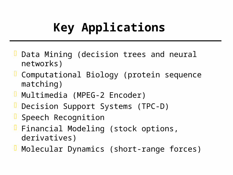
Key Applications
Data Mining (decision trees and neural networks)
Computational Biology (protein sequence matching)
Multimedia (MPEG-2 Encoder) Decision Support Systems (TPC-D)Speech RecognitionFinancial Modeling (stock options, derivatives)Molecular Dynamics (short-range forces)

Example App: Protein Matching
Problem: Find areas of database protein chains that match (modulo some mutations) the sample protein chains

How the Algorithm Works
Generate most-likely mutations
Pick 4 consecutive amino acids from sample
GDSL
GDSI GDSM
ADSI AESI
AETI GETM

Example App: Protein Matching
If match is found: try to extend it
Compare them to every positions in the database proteins

How to Use MLD
Main compute engine of the machine Add a traditional processor to DRAM chip
Incremental gains Include a special (vector/multi) processor Hard to
program
UC Berkeley: IRAMNotre Dame: Execube, PetaflopsMIT: RawStanford: Smart Memories

How to Use MLD (II)
Co-processor, special-purpose processor ATM switch controller Process data beside the disk Graphics accelerator
Stanford: ImagineUC Berkeley: ISTORE

How to Use MLD (III)
Our approach: replace memory chips PIM chip processes the memory-intensive parts
of the program
Illinois: FlexRAMUC Davis: Active PagesUSC-ISI: DIVA
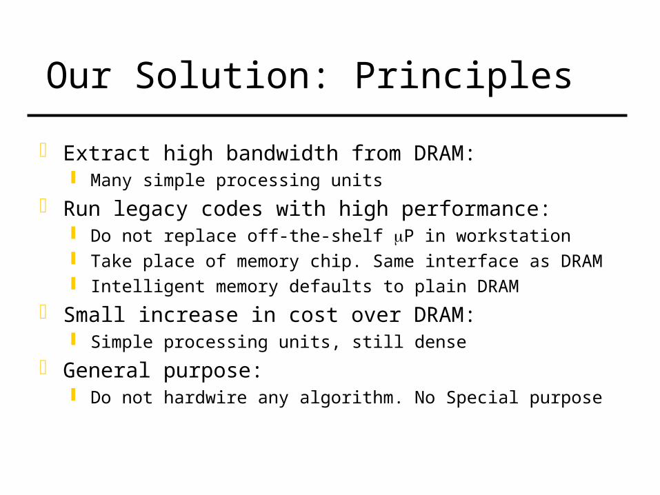
Our Solution: Principles
Extract high bandwidth from DRAM: Many simple processing units
Run legacy codes with high performance: Do not replace off-the-shelf P in workstation Take place of memory chip. Same interface as DRAM Intelligent memory defaults to plain DRAM
Small increase in cost over DRAM: Simple processing units, still dense
General purpose: Do not hardwire any algorithm. No Special purpose

Architecture Proposed

Chip Organization
•Organized in 64 1-Mbyte banks
•Each bank:
•Associated to 1 P.Array
•1 single port
•2 row buffers (2KB)
•P.Array access: 10ns (RB hit) 20ns (miss)
•On-chip memory b/w 102GB/s
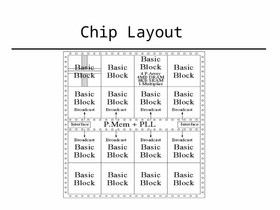
Chip Layout

Basic Block
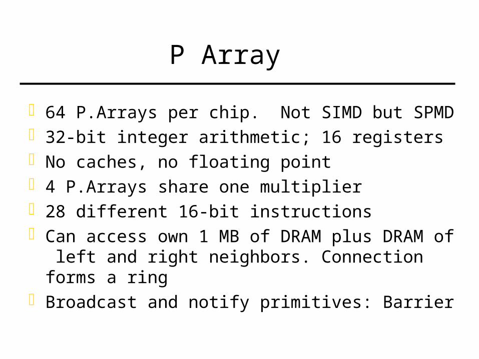
P Array
64 P.Arrays per chip. Not SIMD but SPMD32-bit integer arithmetic; 16 registersNo caches, no floating point4 P.Arrays share one multiplier28 different 16-bit instructionsCan access own 1 MB of DRAM plus DRAM of
left and right neighbors. Connection forms a ring
Broadcast and notify primitives: Barrier

Instruction Memory
Group of 4 P.Arrays share one 8-Kbyte, 4-ported SRAM instruction memory (not I-cache) Holds the P.Array code Small because short code Aggressive access time: 1 cycle = 2.5 ns

P Mem
2-issue in-order: PowerPC 603 16KB I,D caches
Executes serial sectionsCommunication with P.Arrays:
Broadcast/notify or plain write/read to memory Communication with other P.Mems:
Memory in all chips is visibleAccess via the inter-chip networkMust flush caches to ensure data coherence

Area Estimation (mm )
PowerPC 603+caches: 12
SRAM instruction memory: 34
64 Mbytes of DRAM: 330
P.Arrays: 96
Pads + network interf. + refresh logic 20
Rambus interface: 3.4Multipliers: 10
Total = 505
Of which 28% logic, 65% DRAM, 7% SRAM
2
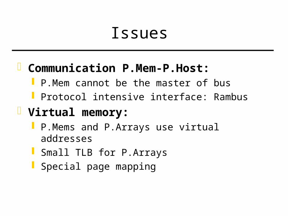
Issues
Communication P.Mem-P.Host: P.Mem cannot be the master of bus Protocol intensive interface: Rambus
Virtual memory: P.Mems and P.Arrays use virtual addresses Small TLB for P.Arrays Special page mapping

EvaluationP.Host P.Host L1 & L2 Bus & Memory Freq: 800 MHz L1 Size: 32 KB Bus: Split Trans Issue Width: 6 L1 RT: 2.5 ns Bus Width: 16 B Dyn Issue: Yes L1 Assoc: 2 Bus Freq: 100 MHz I-Window Size: 96 L1 Line: 64 B Mem RT: 262.5 ns Ld/St Units: 2 L2 Size: 256 KB Int Units: 6 L2 RT: 12.5 ns FP Units: 4 L2 Assoc: 4 Pending Ld/St: 8/8 L2 Line: 64 B BR Penalty: 4 cyc P.Mem P.Mem L1 P.Array Freq: 400 MHz L1 Size: 16 KB Freq: 400 MHz Issue Width: 2 L1 RT: 2.5 ns Issue Width: 1 Dyn Issue: No L1 Assoc: 2 Dyn Issue: No Ld/St Units: 2 L1 Line: 32 B Pending St: 1 Int Units: 2 L2 Cache: No Row Buffers: 3 FP Units: 2 RB Size: 2 KB Pending Ld/St: 8/8 RB Hit: 10 ns BR Penalty: 2 cyc RB Miss: 20 ns

Speedups
Constant Problem Size Scaled Problem Size

Utilization
Low P.Host Utilization

Utilization
High P.Array Utilization Low P.Mem Utilization

Speedups
Varying Logic Frequency

Problems & Future Work
Fabrication technology heat, power dissipation, effect of logic noise on memory, package, yield, cost
Fault tolerance defect memory bank, processor
Compiler, Programming Language.

Conclusion
We have a handle on: A promising technology (MLD) Key applications of industrial interest
Real chance to transform the computing landscape
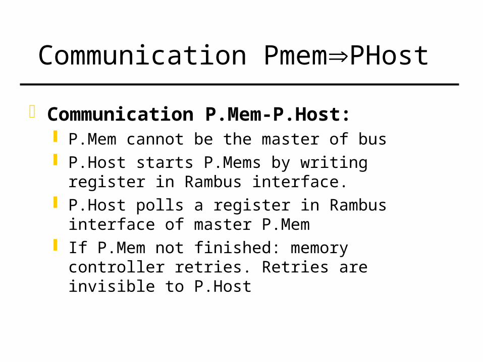
Communication PmemPHost
Communication P.Mem-P.Host: P.Mem cannot be the master of bus P.Host starts P.Mems by writing register in
Rambus interface. P.Host polls a register in Rambus interface of
master P.Mem If P.Mem not finished: memory controller
retries. Retries are invisible to P.Host

Virtual Address Translation