July 2007 Rev 2 1/426
UM0339User manual
SuperH™ (SH) 32-bit RISC seriesSH-4, ST40 system architecture, volume 1: system
This manual describes the ST40 family system architecture. It is split into four volumes:
ST40 System Architecture - Volume 1 System - ADCS 7153464.
ST40 System Architecture - Volume 2 Bus Interfaces - ADCS 7181720.
ST40 System Architecture - Volume 3 Video Devices - ADCS 7225754.
ST40 System Architecture - Volume 4 I/O Devices - ADCS 7225754.
www.st.com
PRELIMINARY DATA
Contents
Preface xxi
Document identification and control xxiST40 documentation suite xxi
ST40 Micro Toolset User’s Guide xxiOS21 User’s Manual xxiiOS21 for ST40 User Manual xxii32-Bit RISC Series, SH-4 CPU Core Architecture xxii32-Bit RISC Series, SH-4, ST40 System Architecture xxii
Conventions used in this guide xxiiiGeneral notation xxiiiHardware notation xxiiiSoftware notation xxiii
1 Overview 1
1.1 ST40 features 11.2 Block diagram 2
1.2.1 CPU 31.2.2 FPU/MAC 31.2.3 MMU 4
1.2.4 Cache 41.2.5 Interrupt 51.2.6 DMA controller 5
STMicroelectronicsADCS 7153464G SH-4, ST40 System Architecture, Volume 1: System
viPRELIMINARY DATA
1.2.7 Debugging and emulation 51.2.8 Power management 61.2.9 Timers 61.2.10 Real-time clock 61.2.11 Serial communication 6
1.2.12 External memory support 6
2 System organization 7
2.1 The SuperHyway 72.1.1 SuperHyway architecture 72.1.2 Packets 92.1.3 Transactions 10
RequestResponseA complete transaction
2.1.4 SuperHyway packet-router 13
2.2 Physical address map 13
3 Interrupt controller (INTC) 15
3.1 Overview 153.1.1 INTC features 153.1.2 Block diagram 16
3.1.3 Pin configuration 173.1.4 Register configuration 17
3.2 Interrupt sources 193.2.1 NMI interrupts 193.2.2 IRL interrupts 203.2.3 On-chip peripheral module interrupts 22
3.2.4 Interrupt exception handling and priority 23
3.3 INTC registers 263.3.1 Interrupt priority registers A to D (IPRA to IPRD) 263.3.2 Interrupt control register (ICR) 27
STMicroelectronicsSH-4, ST40 System Architecture, Volume 1: System ADCS 7153464G

viiPRELIMINARY DATA
Bit 15: NMI input level (NMIL)Bit 14: NMI interrupt mask (MAI)Bit 9: NMI block mode (NMIB)Bit 8: NMI edge select (NMIE)Bit 7: IRL pin modeBits 13 to 10 and 6 to 0: reserved
3.3.3 Interrupt priority registers (INTPRI00, INTPRI04, INTPRI08) 30
3.3.4 Interrupt request registers (INTREQ00, INTREQ04, INTREQ08) 32
3.3.5 Interrupt mask registers (INTMSK00, INTMSK04, INTMSK08) 34
3.3.6 Interrupt mask clear registers (INTMSKCLR00, INTMSKCLR04, INTMSKCLR08) 36
3.3.7 INTC2 mode register (INTC2MODE) 38
3.4 INTC operation 403.4.1 Interrupt sequence 403.4.2 Multiple interrupts 42
4 GPDMA controller (DMAC) 43
4.1 Features 434.2 Address map 45
4.2.1 Channel 0: multiplexed DMA channel 47
4.2.2 Channels 1 to 4: linked list DMA channel 49
4.3 Peripheral allocation 504.4 DMA operation 51
4.4.1 DMA transfer procedure 51StallErrorDisableCompletion
4.4.2 DMA transfer units 53
4.4.3 DMA timing model 53Free-runningTriggered
STMicroelectronicsADCS 7153464G SH-4, ST40 System Architecture, Volume 1: System

viiiPRELIMINARY DATA
Paced
4.4.4 DMA requests 544.4.5 DMA data organization 55
Single location/0DIncrementing/1DRectangular array/2D
4.4.6 Endianness 57
4.4.7 DMA channel arbitration 574.4.8 Extension to basic DMA operations 57
Single linked listMultiplexed channels
4.5 Interfaces 604.6 Register descriptions 61
4.6.1 Global registers 62DMA.VCR.STATUSDMA.VCR.VERSIONDMA.ENABLEDMA.DISABLEDMA.STATUSDMA.INTERRUPTDMA.ERRORDMA.DEFINEDDMA.HANDSHAKE
4.6.2 Channel specific registers 71DMA.CHAN[n].IDENTITYDMA.CHAN[n].ENABLEDMA.CHAN[n].DISABLEDMA.CHAN[n].STATUSDMA.CHAN[n].ACTIONDMA.CHAN[n].POINTERDMA.CHAN[n].REQUESTDMA.CHAN[n].SUBBASEDMA.CHAN[n].SUBENABLEDMA.CHAN[n].SUBDISABLEDMA.CHAN[n].SUB_INTENBDMA.CHAN[n].SUBINT_DISDMA.CHAN[n].SUBINT_STATDMA.CHAN[n].SUBINT_ACT
4.6.3 Memory mapped channel registers 93
STMicroelectronicsSH-4, ST40 System Architecture, Volume 1: System ADCS 7153464G

ixPRELIMINARY DATA
DMA.CHAN[n].CONTROLDMA.CHAN[n].COUNTDMA.CHAN[n].SARDMA.CHAN[n].DARDMA.CHAN[n].NEXT_PTRDMA.CHAN[n].SRC_LENGTHDMA.CHAN[n].SRC_STRIDEDMA.CHAN[n].DST_LENGTHDMA.CHAN[n].DST_STRIDE
5 Parallel input/output (PIO) 107
5.1 PIO ports 0 to 2 1075.2 Register descriptions 109
5.2.1 Output registers 1095.2.2 Input registers 1125.2.3 Configuration registers 1135.2.4 PIO input compare and compare mask registers 116
5.2.5 Pseudoregisters 118
6 Clock and power management 121
6.1 Overview 1216.2 Address map 122
6.2.1 CPG bank 122
6.2.2 CLKGEN bank 123
6.3 Clock functionality 1256.3.1 Internal organization 1256.3.2 PLL1 control 127
DiagramIntroductionAllowable transitionsState definitionsEnabling and disabling PLL1Changing PLL1 divide ratios (clk1 to 3)Changing the PLL1 divide ratio for clock 14Changing PLL1 lock frequency
STMicroelectronicsADCS 7153464G SH-4, ST40 System Architecture, Volume 1: System
xPRELIMINARY DATA
PLL frequency calculation
6.3.3 Configuring PLL2 132IntroductionProcedure to enable and disable PLL2Changing the frequency of PLL2
6.3.4 Register description 134Frequency control register 1 (CPG.FRQCR)CLKGEN.PLL1CR1CLKGEN.PLL1CR2CLKGEN.PLL2CRCLOCKGEN.CLK4CRCLOCKGEN.CPGBYPASSCLKGEN.PLL2_MUXCRCLKGEN.CLK1CRCLKGEN.CLK2CRCLKGEN.CLK3CRCLKGEN.CLK_SELCR
6.4 Watchdog timer 1536.4.1 Block diagram 1536.4.2 Register configuration 1546.4.3 Register descriptions 154
Watchdog timer counter (CPG.WTCNT)Watchdog timer control and status register (CPG.WTCSR)Bit 7: timer enable (TME)Bit 6: timer mode select (WT/NOT_IT)Bit 5: reset select (RSTS)Bit 4: watchdog timer overflow flag (WOVF)Bit 3: interval timer overflow flag (IOVF)Bits 2 to 0: clock select 2 to 0 (CKS2 to CKS0)Writing to CPG.WTCNT and CPG.WTCSR
6.4.4 Using the WDT 159Standby clearing procedureFrequency changing procedureUsing watchdog timer modeUsing interval timer mode
6.5 Power management unit (PMU) 1616.5.1 Types of power-down modes 1626.5.2 Register configuration 164
STMicroelectronicsSH-4, ST40 System Architecture, Volume 1: System ADCS 7153464G

xiPRELIMINARY DATA
6.5.3 Pin configuration 1656.5.4 Register descriptions 165
Standby control register (CPG.STBCR)Bit 7: standby (STBY)Bit 6: peripheral module pin high impedance control (PHZ)Bit 5: peripheral module pin pull-up control (PPU)Bit 4: unusedBit 3: module stop 3 (MSTP3)Bit 2: module stop 2 (MSTP2)Bit 1: module stop 1 (MSTP1)Bit 0: module stop 0 (MSTP0)Peripheral module pin pull-up controlStandby control register 2 (CPG.STBCR2)Bit 7: unusedBit 6: status pin high-impedance control (STHZ)Bits 5 to 2: reservedBit 1: module stop 6 (MSTP6)Bit 0: module stop 5 (MSTP5)Standby control request register (CLOCKGEN.STBREQCR)Standby control acknowledge register (CLOCKGEN.STBACKCR)
6.6 Functionality 1716.6.1 Sleep mode 171
Transition to sleep modeExit from sleep modeExit by interruptExit by reset
6.6.2 Deep sleep mode 172Transition to deep sleep modeExit from deep sleep mode
6.6.3 Standby mode 172Transition to standby modeExit from standby modeExit by interruptExit by reset
6.6.4 Clock pause function 174
6.7 Module standby function 175
STMicroelectronicsADCS 7153464G SH-4, ST40 System Architecture, Volume 1: System
xiiPRELIMINARY DATA
6.7.1 Transition to module standby function(CPG modules) 175
6.7.2 Transition to module standby function (CLOCKGEN modules) 176
6.7.3 Exit from module standby function(CPG modules) 176
6.7.4 Exit from module standby function(CLOCKGEN modules) 177
6.8 STATUS pin change timing 177
7 Real-time clock (RTC) 179
7.1 Overview 1797.1.1 Features 179
7.1.2 Block diagram 1817.1.3 Pin configuration 1827.1.4 Register configuration 1827.1.5 Register initialization 184
7.2 Register descriptions 1857.2.1 64 Hz counter (RTC.R64CNT) 185
7.2.2 Second counter (RTC.RSECCNT) 1867.2.3 Minute counter (RTC.RMINCNT) 1887.2.4 Hour counter (RTC.RHRCNT) 1907.2.5 Day-of-week counter (RTC.RWKCNT) 192
7.2.6 Day counter (RTC.RDAYCNT) 1947.2.7 Month counter (RTC.RMONCNT) 1967.2.8 Year counter (RTC.RYRCNT) 1987.2.9 Second alarm register (RTC.RSECAR) 2007.2.10 Minute alarm register (RTC.RMINAR) 202
7.2.11 Hour alarm register (RTC.RHRAR) 2047.2.12 Day-of-week alarm register (RTC.RWKAR) 2067.2.13 Day alarm register (RTC.RDAYAR) 2087.2.14 Month alarm register (RTC.RMONAR) 210
7.2.15 RTC control register 1 (RTC.RCR1) 2127.2.16 RTC control register 2 (RTC.RCR2) 215
STMicroelectronicsSH-4, ST40 System Architecture, Volume 1: System ADCS 7153464G
xiiiPRELIMINARY DATA
7.3 Operation 2197.3.1 Time setting procedures 2197.3.2 Time reading procedures 2217.3.3 Alarm function 222
7.4 Interrupts 2237.5 Usage notes 223
7.5.1 Register initialization 2237.5.2 Crystal oscillator circuit 224
8 Timer unit (TMU) 227
8.1 Overview 2278.1.1 Features 2278.1.2 Block diagram 229
8.1.3 Pin configuration 2298.1.4 Register configuration 230
8.2 Register descriptions 2328.2.1 Timer output control register (TMU.TOCR) 2328.2.2 Timer start register (TMU.TSTR) 2338.2.3 Timer constant registers (TMU.TCOR) 234
8.2.4 Timer counters (TMU.TCNT) 2358.2.5 Timer control registers (TMU.TCR) 2368.2.6 Input capture register (TMU.TCPR2) 243
8.3 Operation 2448.3.1 Counter operation 244
Example of count operation setting procedureAuto-reload count operationTCNT count timing
8.3.2 Input capture function 248
8.4 Interrupts 2498.5 Usage notes 250
8.5.1 Register writes 2508.5.2 TCNT register reads 250
STMicroelectronicsADCS 7153464G SH-4, ST40 System Architecture, Volume 1: System

xivPRELIMINARY DATA
8.5.3 Resetting the RTC frequency divider 2508.5.4 External clock frequency 250
9 Serial communication interface with FIFO(SCIF) 251
9.1 Overview 2519.1.1 Features 2519.1.2 Block diagram 2539.1.3 Pin configuration 2549.1.4 Register configuration 255
9.2 Register descriptions 2569.2.1 Receive shift register (SCIF.SCRSR) 256
9.2.2 Receive FIFO data register (SCIF.SCFRDR) 2569.2.3 Transmit shift register (SCIF.SCTSR) 2579.2.4 Transmit FIFO data register (SCIF.SCFTDR) 2589.2.5 Serial mode register (SCIF.SCSMR) 259
Bits 15 to 7: reservedBit 6: character length (CHR)Bit 5: parity enable (PE)Bit 4: parity mode (O/E)Bit 3: stop bit length (STOP)Bit 2: reservedBits 1 and 0: clock select 1 and 0 (CKS1, CKS0)
9.2.6 Serial control register (SCIF.SCSCR) 264Bits 15 to 8 and 2: reservedBit 7: transmit interrupt enable (TIE)Bit 6: receive interrupt enable (RIE)Bit 5: transmit enable (TE)Bit 4: receive enable (RE)Bit 3: receive error interrupt enable (REIE)Bit 2: reservedClock enable (CKE0 and CKE1)
9.2.7 Serial status register (SCIF.SCFSR) 270Bits 15 to 12: number of parity errors (PER3 to PER0)Bits 11 to 8: number of framing errors (FER3 to FER0)Bit 7: receive error (ER)
STMicroelectronicsSH-4, ST40 System Architecture, Volume 1: System ADCS 7153464G

xvPRELIMINARY DATA
Bit 6: transmit end (TEND) Bit 5: transmit-FIFO-data-empty (TDFE)Bit 4: break detect (BRK)Bit 3: framing error (FER)Bit 2: parity error (PER)Bit 1: receive-FIFO-data-full (RDF)Bit 0: receive data ready (DR)
9.2.8 Bit rate register (SCIF.SCBRR) 2829.2.9 FIFO control register (SCIF.SCFCR) 284
Bits 15 to 11: reservedBits 10, 9 and 8: RTS output active trigger (RSTRG2, RSTRG1 and RSTRG0)Bits 7 and 6: receive FIFO data number trigger (RTRG1, RTRG0)Bits 5 and 4: transmit FIFO data number trigger (TTRG1, TTRG0)Bit 3: modem control enable (MCE)Bit 2: transmit FIFO data register reset (TFRST)Bit 1: receive FIFO data register reset (RFRST)Bit 0: loopback test (LOOP)
9.2.10 FIFO data count register (SCIF.SCFDR) 2919.2.11 Serial port register (SCIF.SCSPTR) 293
Bits 15 to 8: reservedBit 7: serial port RTS port I/O (RTSIO)Bit 6: serial port RTS port data (RTSDT)Bit 5: serial port CTS port I/O (CTSIO)Bit 4: serial port CTS port data (CTSDT)Bit 3: serial port clock port data (SCKIO)Bit 2: serial port clock port data (SCKDT)Bit 1: serial port break I/O (SPB2IO)Bit 0: serial port break data (SPB2DT)
9.2.12 Line status register (SCIF.SCLSR) 301Bits 15 to 1: reservedBit 0: overrun error (ORER)
9.3 Operation 3039.3.1 Overview 3039.3.2 Serial operation 305
Data transfer formatClockData transfer operations
STMicroelectronicsADCS 7153464G SH-4, ST40 System Architecture, Volume 1: System

xviPRELIMINARY DATA
Serial data reception
9.4 SCIF interrupt sources and the DMAC 3159.5 Usage notes 316
9.5.1 SCIF.SCFTDR writing and the TDFE flag 3169.5.2 SCIF.SCFRDR reading and the RDF flag 317
9.5.3 Break detection and processing 3179.5.4 Sending a break signal 3179.5.5 Receive data sampling timing and receive margin 3189.5.6 SCK/MRESET 319
9.5.7 When using the DMAC 3199.5.8 Serial ports 319
10 User break controller (UBC) 321
10.1 Overview 32110.1.1 Features 32110.1.2 Block diagram 323
10.2 Register overview 32410.3 Register descriptions 327
10.3.1 Access to UBC control registers 32710.3.2 Break address register A (UBC.BARA) 328
Bits 31 to 0: break address A31 to A0 (BAA31 to BAA0)
10.3.3 Break ASID register A (UBC.BASRA) 329Bits 7 to 0: break ASID A7 to A0 (BASA7 to BASA0)
10.3.4 Break address mask register A (UBC.BAMRA) 329Bits 7 to 4: reservedBit 2: break ASID mask A (BASMA):Bits 3, 1, and 0: break address mask A2 to A0 (BAMA2 to BAMA0):
10.3.5 Break bus cycle register A (UBC.BBRA) 331Bits 15 to 7: reservedBits 5 and 4: instruction access/operand access select A (IDA1, IDA0):Bits 3 and 2: read/write select A (RWA1, RWA0)Bits 6, 1, and 0: operand size select A (SZA2 to SZA0)
STMicroelectronicsSH-4, ST40 System Architecture, Volume 1: System ADCS 7153464G
xviiPRELIMINARY DATA
10.3.6 Break address register B (UBC.BARB) 33310.3.7 Break ASID register B (UBC.BASRB) 33310.3.8 Break address mask register B (UBC.BAMRB) 33310.3.9 Break data register B (UBC.BDRB) 334
Bits 31 to 0: break data B31 to B0 (BDB31 to BDB0):
10.3.10 Break data mask register B (UBC.BDMRB) 335Bits 31 to 0: break data mask B31 to B0 (BDMB31 to BDMB0)
10.3.11 Break bus cycle register B (UBC.BBRB) 33610.3.12 Break control register (UBC.BRCR) 337
Bit 15: condition match flag A (CMFA)Bit 14: condition match flag B (CMFB)Bits 13 to 11: reservedBit 10: instruction access break select A (PCBA)Bits 9 and 8: reservedBit 7: data break enable B (DBEB)Bit 6: PC break select B (PCBB)Bits 5 and 4: reservedBit 3: sequence condition select (SEQ)Bits 2 and 1: reservedBit 0: user break debug enable (UBDE)
10.4 Operation 34110.4.1 Explanation of terms relating to accesses 34110.4.2 Explanation of terms relating to instruction intervals 341
Example of sequence of instructions with no branchExample of sequence of instructions with a branch
10.4.3 User break operation sequence 34210.4.4 Instruction access cycle break 34410.4.5 Operand access cycle break 345
10.4.6 Condition match flag setting 346Instruction access with post-execution condition, or operand accessInstruction access with pre-execution condition
10.4.7 Program counter (PC) value saved 34710.4.8 Contiguous A and B settings for sequential conditions 348
Instruction access matches on both channel A and channel BInstruction access match on channel A, operand access
STMicroelectronicsADCS 7153464G SH-4, ST40 System Architecture, Volume 1: System
xviiiPRELIMINARY DATA
match on channel BOperand access match on channel A, instruction access match on channel BOperand access matches on both channel A and channel B
10.5 Usage notes 35010.6 User break debug support function 35210.7 Examples of use 353
10.7.1 Instruction access cycle break condition settings 353Independent channel A channel B mode: user break interrupt generatedChannel A channel B sequential mode: user break interrupt generatedIndependent channel A channel B mode: user break interrupts not generated
10.7.2 Operand access cycle break condition settings 35610.7.3 User break controller stop function 35810.7.4 Transition to user break controller stopped state 358
10.7.5 Cancelling the user break controller stopped state 35910.7.6 Examples of stopping and restarting the user break
controller 359
11 User debug interface (UDI) 361
11.1 Overview 36111.1.1 Features 361
11.1.2 Block diagram 36111.1.3 Pin configuration 36311.1.4 Register configuration 364
11.2 Register descriptions 36711.2.1 Instruction register (SDIR) 367
Bits 15 to 8:Test instruction bits (TI7 to TI0)Bits 7 to 0: reserved
11.2.2 Data register (SDDR) 370Bits 31 to 0: DR Data
11.2.3 Bypass register (SDBPR) 371
STMicroelectronicsSH-4, ST40 System Architecture, Volume 1: System ADCS 7153464G
xixPRELIMINARY DATA
11.2.4 Interrupt factor register (SDINT) 371Bits 15 to 1: reservedBit 0: interrupt request bit (INTREQ)
11.2.5 Boundary scan register (SDBSR) 372
11.3 Operation 37211.3.1 TAP control 37211.3.2 UDI reset 37311.3.3 UDI interrupt 37411.3.4 Bypass 37411.3.5 Boundary scan (EXTEST, SAMPLE/RELOAD) 374
11.4 Usage notes 37511.4.1 SDIR command 37511.4.2 SDIR commands in sleep mode 37511.4.3 Emulator 375
12 Advanced user debugger (AUD) 377
12.1 Overview 37712.1.1 Features 377
12.1.2 Block diagram 378
12.2 AUD interface pins 37912.3 Register summary 380
13 ASE hardware break controller 381
13.1 Overview 38113.1.1 Features 381
13.1.2 Differences between the user break controller and ASE hardware break controller 382
13.1.3 Block diagram 383
13.2 Register summary 384
STMicroelectronicsADCS 7153464G SH-4, ST40 System Architecture, Volume 1: System

xxPRELIMINARY DATA
Appendices
A ST40 system architectural conventions 389
A.1 Introduction 389A.1.1 Memory blocks 389A.1.2 Control registers 390
Register conventionsField conventionsControl register layout
A.1.3 Version control registers 394A.1.4 P-ERROR flags 397A.1.5 M-ERROR flags 401A.1.6 Memory map conventions 401A.1.7 P-MODULE specification standards 402
B Register address list 403
Index 417
STMicroelectronicsSH-4, ST40 System Architecture, Volume 1: System ADCS 7153464G
PRELIMINARY DATA
Preface
This document is part of the SuperH Documentation Suite detailed below. Comments on this or other manuals in the SuperH Documentation Suite should be made by contacting your local STMicroelectronics Limited Sales Office or distributor.
Document identification and controlEach book carries a unique identifier in the form:
ADCS nnnnnnnx
Where, nnnnnnn is the document number and x is the revision.
Whenever making comments on a document the complete identification ADCS nnnnnnnx should be quoted.
ST40 documentation suiteThe ST40 documentation suite comprises the following volumes:
ST40 Micro Toolset User’s Guide
ADCS 7379953. This manual provides an introduction to the ST40 Micro Toolset and instructions for getting a simple OS21 application run on an STMicroelectronics’ MediaRef platform. It also describes how to boot OS21 applications from ROM and how to port applications which use STMicroelectronics’ STLite/OS20 operating systems to OS21.
STMicroelectronicsADCS 7153464G SH-4, ST40 System Architecture, Volume 1: System
xxiiPRELIMINARY DATA
OS21 User’s Manual
ADCS 7358306. This manual describes the generic use of OS21 across supported platforms. It describes all the core features of OS21and their use and details the OS21 function definitions.It also explains how OS21 differs to STLite/OS20, the API targeted at ST20.
OS21 for ST40 User Manual
ADCS 7358673. This manual describes the use of OS21 on ST40 platforms. It describes how specific ST40 facilities are exploited by the OS21 API. It also describes the OS21 board support packages for ST40 platforms.
32-Bit RISC Series, SH-4 CPU Core Architecture
ADCS 7182230. This manual describes the architecture and instruction set of the SH4-1xx (previously known a ST40-C200) core as used by STMicroelectronics.
32-Bit RISC Series, SH-4, ST40 System Architecture
This manual describes the ST40 family system architecture. It is split into four volumes:
ST40 System Architecture - Volume 1 System - ADCS 7153464.
ST40 System Architecture - Volume 2 Bus Interfaces - ADCS 7171720.
ST40 System Architecture - Volume 3 Video Devices - ADCS 7225754.
ST40 System Architecture - Volume 4 I/O Devices - ADCS 7225754.
STMicroelectronicsSH-4, ST40 System Architecture, Volume 1: System ADCS 7153464G

xxiiiPRELIMINARY DATA
Conventions used in this guide
General notation
The notation in this document uses the following conventions:
• Sample code, keyboard input and file names,
• Variables and code variables,
• Equations and math,
• Screens, windows and dialog boxes,
• Instructions.
Hardware notation
The following conventions are used for hardware notation:
• REGISTER NAMES and FIELD NAMES,
• PIN NAMES and SIGNAL NAMES.
Software notation
Syntax definitions are presented in a modified Backus-Naur Form (BNF). Briefly:
1 Terminal strings of the language, that is those not built up by rules of the lan-guage, are printed in teletype font. For example, void.
2 Nonterminal strings of the language, that is those built up by rules of the lan-guage, are printed in italic teletype font. For example, name.
3 If a nonterminal string of the language starts with a nonitalicized part, it is equivalent to the same nonterminal string without that nonitalicized part. For example, vspace-name.
4 Each phrase definition is built up using a double colon and an equals sign to sep-arate the two sides.
5 Alternatives are separated by vertical bars (‘|’).
6 Optional sequences are enclosed in square brackets (‘[’ and ‘]’).
7 Items which may be repeated appear in braces (‘’ and ‘’).
STMicroelectronicsADCS 7153464G SH-4, ST40 System Architecture, Volume 1: System

xxivPRELIMINARY DATA
STMicroelectronicsSH-4, ST40 System Architecture, Volume 1: System ADCS 7153464G

PRELIMINARY DATA
STMicroelectroniADCS 7153464G SH-4, ST40 S
1
Overview1.1 ST40 features The ST40 product family integrates a 32-bit RISC (reduced instruction set computer) microprocessor with a rich set of peripherals.
The processor implements the SH-4 instruction set and has object code upward- compatibility with earlier SH family of architectures. The CPU is coupled with an 8-kbyte I-cache, a 16-kbyte D-cache, an MMU and an FPU with support for floating point 3D-geometry acceleration.
The ST40 product family provides development support functions with a full range of debug features and an emulation mode (ASE). The ASE mode has a dedicated 1KB buffer for emulator firmware, supporting performance counters and branch trace.
The ST40 product family supports Microsoft’s WinCE and other operating systems with little requirement for external logic.
csystem Architecture, Volume 1: System
2 Block diagramPRELIMINARY DATA
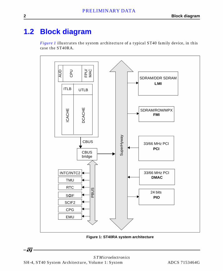
1.2 Block diagramFigure 1 illustrates the system architecture of a typical ST40 family device, in this case the ST40RA.
Figure 1: ST40RA system architecture
ITLB UTLB
ICA
CH
E
DC
AC
HE
INTC/INTC2
TMU
RTC
SCIF
SCIF2
CPG
EMU
PIO
DMAC
PCI
SDRAM/ROM/MPXFMI
LMI
CP
U
AU
D
FP
U/
Sup
erH
yway
MA
C
CBUSbridge
CBUS
1
SDRAM/DDR SDRAM
33/66 MHz PCI
24 bits
33/66 MHz PCI
PB
US
STMicroelectronicsSH-4, ST40 System Architecture, Volume 1: System ADCS 7153464G
Block diagram 3PRELIMINARY DATA
The features of the ST40 product family are summarized below.
1.2.1 CPU
The CPU has the following features:
• SH-4 32-bit RISC architecture,
• operating frequency of 160 MHz,
• 2 way superscalar architecture,
• high code density using fixed length 16-bit instruction,
• load-store architecture,
• delayed branch instructions,
• on-chip multiplier,
• five-stage pipeline.
1.2.2 FPU/MAC
The FPU/MAC is an on-chip floating-point coprocessor which has the following features:
• support for single-precision (32-bit) and double-precision (64-bit),
• support forIEEE754-compliant data types and exceptions,
• 2 rounding modes:
- round to nearest,
- round to zero,
• handling of denormalized numbers:
- truncation to zero,
- interrupt generation for compliance with IEEE754,
• FMAC (multiply-and- accumulate), FDIV (divide) and FSQRT (square root) instructions,
STMicroelectronicsADCS 7153464G SH-4, ST40 System Architecture, Volume 1: System

4 Block diagramPRELIMINARY DATA
• 3-D graphics instructions (single-precision):
- 4-dimensional vector conversion and matrix operations (FTRV), 4 cycles (pitch), 7 cycles (latency),
- 4-dimensional vector (FIPR) inner product, 1 cycle (pitch), 4 cycles (latency),
• Five-stage pipeline.
1.2.3 MMU
The MMU has the following features:
• 4 Gbytes of address space with 256 address space identifiers (8-bit ASIDs),
• single virtual mode and multiple virtual memory mode,
• support for multiple page sizes:
- 1 Kbyte,
- 4 Kbytes,
- 64 Kbytes,
- 1 Mbyte,
• 4-entry fully-associative ITLB for instructions,
• 64-entry fully-associative UTLB for instructions and operands,
• support for software-controlled replacement and random-counter replacement algorithms.
1.2.4 Cache
The ST40 product family has the following cache features:
• 8 Kbytes, direct-mapped instruction cache organized as 256 32 byte lines,
• 16 Kbytes, direct-mapped operand cache:
- organized as 512 32 byte lines,
- RAM mode (8 kbytes of cache plus 8 Kbytes of RAM),
- selectable write method copy-back or write-through,
• single-stage copy-back buffer, single- stage write-through buffer,
STMicroelectronicsSH-4, ST40 System Architecture, Volume 1: System ADCS 7153464G

Block diagram 5PRELIMINARY DATA
• address-mapped cache contents,
• store queue of 32 bytes, 2 entries.
1.2.5 Interrupt
The ST40 product family has the following interrupts:
• 5 independent external interrupts (NMI, IRL3 to IRL0),
• IRL3 to IRL0 configured either as 4 independent interrupts or encoded to provide 15 external interrupt levels,
• on-chip peripheral module interrupts, where the priority level can be set for each module.
1.2.6 DMA controller
The 5-channel physical address DMA controller has the following features:
• 4 general-purpose channels which will perform memory-to-memory or memory-to-peripheral transfers,
• 1 buffered multiplexed channel,
• support for 2D block moves and linked lists.
1.2.7 Debugging and emulation
The ST40 product family has the following debug and emulation features:
• debugging by means of user break interrupts,
• 2 break channels,
• address, data value, access type, and data size can all be set as break conditions,
• supports sequential break function,
• uses Hitachi user debug interface (UDI):
- 5-pin serial interface conformant to JTAG, IEEE Standard TAP and boundary scan architecture,
- supports emulator connection,
- provides host access to the 1KB ASERAM for emulator firmware (accessible only in ASE mode).
STMicroelectronicsADCS 7153464G SH-4, ST40 System Architecture, Volume 1: System
6 Block diagramPRELIMINARY DATA
1.2.8 Power management
The ST40 product family uses the following power management features:
• software configurable PLL,
• dynamically programmable operating frequencies,
• power-down modes:
- 2 sleep modes,
- standby mode,
- module standby function.
1.2.9 Timers
The 3-channel auto-reload 32-bit timer unit has:
• input capture function,
• choice of 7 counter input clocks.
1.2.10 Real-time clock
The real-time clock has the following features:
• on-chip clock and calendar functions,
• built-in 32 kHz crystal oscillator with maximum 1/256 second resolution (cycle interrupts).
1.2.11 Serial communication
The 2 full-duplex communication channels (SCIF1, SCIF2) have the following functions:
• support for asynchronous mode,
• separate FIFOs (16 bytes) provided for transmitter and receiver.
1.2.12 External memory support
See the relevant product datasheet for details.
STMicroelectronicsSH-4, ST40 System Architecture, Volume 1: System ADCS 7153464G

PRELIMINARY DATA
STMicroelectroniADCS 7153464G SH-4, ST40 S
2
System organization 2.1 The SuperHywayThe ST40 system is based around a highly reusable modular structure. Any ST40, implementation, such as the ST40RA chip, is built from a number of modules, in other words peripheral devices, which communicate with each other using 1 or more interconnects. This interconnect provides a memory-mapped packet routing mechanism between modules and is organized to maximize system performance whilst minimizing system cost. As the interface between the interconnect and the modules is highly standardized, the issues associated with integrating families of peripherals with the ST40 processing unit is simplified.
2.1.1 SuperHyway architecture
The SuperHyway architecture provides the ‘glue’ that binds together an ST40 processor with peripheral modules. A connection between the SuperHyway and an on-chip module is called a SuperHyway port. A port supports a bidirectional flow of packets between the SuperHyway and modules.
The distinction between the SuperHyway architecture and implementation is important. This section, defines the abstractions that are used to build implementations containing a packet-routed interconnect. The architecture includes an abstract view of the packets, the packet-router, the port, a peripheral module and the packet-router protocol. The implementation determines how the packet-router, the ports and the required modules are physically represented. It also defines how many modules are implemented and how these are connected to the SuperHyway packet-router.
csystem Architecture, Volume 1: System

8 The SuperHywayPRELIMINARY DATA
Each ST40 device comprises a packet-router and at least 1 module. Each module is connected to the packet-router using at least 1 port. The packet-router provides complete connectivity between modules.
The architectural relationship between the packet-router, the port and the module is illustrated in Figure 2.
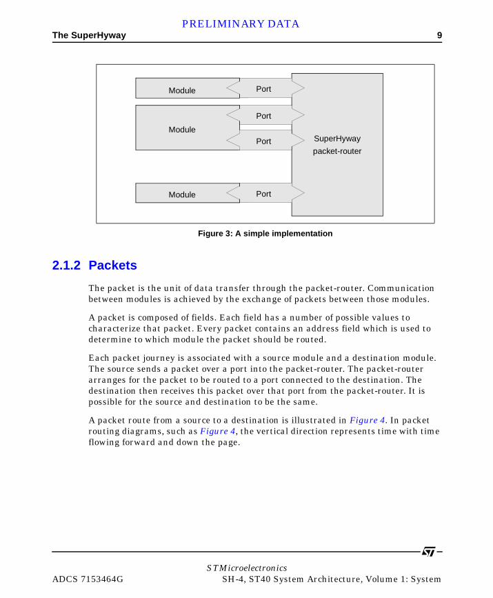
A simple implementation containing a packet-router, 2 single-ported modules and 1 double-ported module is illustrated in Figure 3.
Figure 2: Packet-router, SuperHyway port and ST40RA module architecture
packet-router
Port
Module
Module
A packet-router isconnected to
ports.
A port connectsa packet-router to a
module.
A module isconnected to 1or more ports.
SuperHyway
STMicroelectronicsSH-4, ST40 System Architecture, Volume 1: System ADCS 7153464G
The SuperHyway 9PRELIMINARY DATA
2.1.2 Packets
The packet is the unit of data transfer through the packet-router. Communication between modules is achieved by the exchange of packets between those modules.
A packet is composed of fields. Each field has a number of possible values to characterize that packet. Every packet contains an address field which is used to determine to which module the packet should be routed.
Each packet journey is associated with a source module and a destination module. The source sends a packet over a port into the packet-router. The packet-router arranges for the packet to be routed to a port connected to the destination. The destination then receives this packet over that port from the packet-router. It is possible for the source and destination to be the same.
A packet route from a source to a destination is illustrated in Figure 4. In packet routing diagrams, such as Figure 4, the vertical direction represents time with time flowing forward and down the page.
Figure 3: A simple implementation
PortPortPort
Port
Port
Port
packet-router
Module
Module
Module
SuperHyway
Port
Port
Port
STMicroelectronicsADCS 7153464G SH-4, ST40 System Architecture, Volume 1: System

10 The SuperHywayPRELIMINARY DATA
2.1.3 Transactions
A transaction is an exchange of packets that allows a module to access the state of another module using the packet-router protocol. A transaction consists of the transfer of a request packet from an initiator module to a target module, followed by the transfer of a response packet from that target module back to the initiator module. The request packet initiates the transaction and its contents determine the access to be made. The response packet completes the transaction and its contents indicate the result of the access.
This style of communication is called split phase. The separation between the request packet and the response packet allows systems to be constructed which are tolerant of high latency modules. A requesting module can send multiple requests into the packet-router before any responses are received. This is known as request pipelining and allows the latencies of those transactions to be overlapped.
There is a causal relationship between a request packet and its corresponding response packet since the request packet must be received before the response packet can be sent. Additionally, there is a 1-to-1 correspondence between request packets and response packets.
When a response packet is received by the module that sent the corresponding request, the transaction is complete. It is guaranteed that the destination module has committed to the access associated with the response. This means that, apart from internal latency inside the target module, the access is completed as viewed through all ports to that module. Any subsequent requests to that target module will therefore act after that access. This guarantee means that time-ordering of accesses at a destination can be imposed by waiting for the corresponding response.
Figure 4: A packet route
Source module
PacketDestination module
Packet-router
Packet routed from sourceto packet-router over a port
Packet routed from packet-router to destination over a portPacket
Packet
STMicroelectronicsSH-4, ST40 System Architecture, Volume 1: System ADCS 7153464G
The SuperHyway 11PRELIMINARY DATA
A response packet may also indicate whether the request was valid or not. Some implementations of the SuperHyway allow the transmission of special error responses when the target cannot process the request.
The following sections elaborate on the actions comprising a single transaction.
Request
A request packet is constructed by an initiator (also known as a requester) module when that module needs to make an access to a particular target module. This target module is specified as part of the packet’s address field. The initiator is the source of the request packet and sends that packet into the packet-router. The packet-router arranges for that request packet to be routed from its source to its target. The target receives the request packet from the packet-router and services that access according to the information in the received request packet. The target is known as the responding module because it replies to the request packet using a response packet.
Response
A response packet is constructed by a target module in order to reply to a previous request. The identity of the initiator of that request packet is used to route the response packet. The target module is the source of the response packet and sends that packet into the packet-router. As always, the packet-router arranges for that response packet to be routed from its source to its destination. The destination (i.e. transaction initiator) receives the response packet from the packet-router and matches that response to the original request in order to complete the transaction.
STMicroelectronicsADCS 7153464G SH-4, ST40 System Architecture, Volume 1: System

12 The SuperHywayPRELIMINARY DATA
A complete transaction
A packet routing diagram showing a complete transaction is given in Figure 5.
Figure 5: A transaction
Initiator
Request
Target Packet-router
Request
Request
Response
Response
Response
Transaction initiated
Transaction completed
Access made
module module
STMicroelectronicsSH-4, ST40 System Architecture, Volume 1: System ADCS 7153464G
Physical address map 13PRELIMINARY DATA
2.1.4 SuperHyway packet-router
A variety of SuperHyway packet-router implementations are possible. Implementations include, but are not limited to, a bus, a crossbar and a packet routing network.
All packets passed into the packet-router contain a destination field which is used to route the packet. The packet-router contains a mapping from all possible destination field values to an appropriate port. The mechanism by which this mapping is established and the mapping itself are defined by the implementation.
The packet-router needs to interpret only a few fields of a packet. It must inspect the address field to route the packet. The bulk of the packet does not need to be interpreted by the routing mechanism and is used to convey information between the requesting module and the responding module. The protocol is thus easily extensible.
2.2 Physical address mapSee the relevant product datasheet for this information.
STMicroelectronicsADCS 7153464G SH-4, ST40 System Architecture, Volume 1: System
14 Physical address mapPRELIMINARY DATA
STMicroelectronicsSH-4, ST40 System Architecture, Volume 1: System ADCS 7153464G

PRELIMINARY DATA
STMicroelectroniADCS 7153464G SH-4, ST40 S
3C)
Interrupt controller (INT
3.1 OverviewThe interrupt control system ascertains the priority of interrupt sources and controls interrupt requests to the CPU. The INTC registers set the order of priority of each interrupt, allowing the user to handle interrupt requests according to the user controlled priorities.
3.1.1 INTC features
INTC has the features listed below.
• 15 levels of interrupt priority can be set.
By setting the 3 interrupt-priority registers, the priorities of on-chip peripheral module interrupts can be selected from 15 levels for different request sources.
• NMI noise canceler function is available.
NMI input level bit indicates NMI pin status. By reading this bit in the interrupt exception handler, the pin status can be checked, enabling it to be used as a noise canceler.
• Masking of NMI requests by the SR.BL bit can be set.
It is possible to specify whether NMI requests are to be masked (SH-3 compatible operation) or accepted when the SR.BL bit is 1.
csystem Architecture, Volume 1: System

16 OverviewPRELIMINARY DATA
3.1.2 Block diagram
Figure 6 shows a block diagram of the INTC.
Figure 6: INTC block diagram
INTC
ICRIPR
IPRA to IPRD
INTPRI[n]
Bus interface
RESETOUT
Priorityidentifier
Inputcontrol
4
i3 i2 i1 i0
SR
Interruptrequest
Com
para
tor
Resetsignal
TMURTC
SCIF1SCIF2WDT
UDI
NMI
IRL3 to IRL0
INTREQ[n]INTMSK[n]INTMSKCLR[n]INTC2MODE
STMicroelectronicsSH-4, ST40 System Architecture, Volume 1: System ADCS 7153464G
Overview 17PRELIMINARY DATA
3.1.3 Pin configuration
Table 1 shows the INTC pin configuration.
3.1.4 Register configuration
The INTC has the registers listed in Table 2.
Name Abbreviation I/O Description
Nonmaskable interrupt input pin NMI Input Input of nonmaskable interrupt request signal
Interrupt input pins IRL3 TO IRL0 Input Input of interrupt request signals (maskable by I3 to I0 in the status register (SR))
Table 1: INTC pins
Register name Description TypeInitial
valueAAddress
offsetSize
INTC.ICR Interrupt control,see Section 3.1.1: INTC features on page 15
RW B 0x00 16
INTC.IPRA Interrupt priority level A, see Section 3.3.1: Interrupt priority registers A to D (IPRA to IPRD) on page 26
RW 0x0000 0x04 16
INTC.IPRB Interrupt priority level B,see Section 3.3.1: Interrupt priority registers A to D (IPRA to IPRD) on page 26
RW 0x0000 0x08 16
INTC.IPRC Interrupt priority level C,see Section 3.3.1: Interrupt priority registers A to D (IPRA to IPRD) on page 26
RW 0x0000 0x0C 16
Table 2: INTC and INTC2 registers
STMicroelectronicsADCS 7153464G SH-4, ST40 System Architecture, Volume 1: System

18 OverviewPRELIMINARY DATA
INTC.IPRD Interrupt priority level D,see Section 3.3.1: Interrupt priority registers A to D (IPRA to IPRD) on page 26
RW 0xDA74 0x10 16
INTC2.INTPRI00 Interrupt priority level 00,see Table 6 on page 30
RW 0x00000000 0x00 32
INTC2.INTPRI04 Interrupt priority level 04,see Table 7 on page 31
RW 0x00000000 0x04 32
INTC2.INTPRI08 Interrupt priority level 08,see Table 8 on page 31
RW 0x00000000 0x08 32
INTC2.INTREQ00 Interrupt request level 00,see Table 9 on page 32
RO 0x00000000 0x20 32
INTC2.INTREQ04 Interrupt request level 04,see Table 10 on page 33
RO 0x00000000 0x24 32
INTC2.INTREQ08 Interrupt request level 08,see Table 11 on page 33
RO 0x00000000 0x28 32
INTC2.INTMSK00 Interrupt mask 00,see Table 12 on page 34
RW 0xFFFFFFFF 0x40 32
INTC2.INTMSK04 Interrupt mask 04,see Table 13 on page 35
RW 0xFFFFFFFF 0x44 32
INTC2.INTMSK08 Interrupt mask 08,see Table 14 on page 35
RW 0xFFFFFFFF 0x48 32
INTC2.INTMSKCLR00 Interrupt mask clear 00,see Table 15 on page 36
WO - 0x60 32
INTC2.INTMSKCLR04 Interrupt mask clear 04,see Table 16 on page 37
WO - 0x64 32
Register name Description TypeInitial
valueAAddress
offsetSize
Table 2: INTC and INTC2 registers
STMicroelectronicsSH-4, ST40 System Architecture, Volume 1: System ADCS 7153464G
Interrupt sources 19PRELIMINARY DATA
Note: The unshaded registers control the behavior of interrupts arising from legacy SH peripherals and the shaded registers control the behavior of interrupts arising from peripherals integrated on the SuperHyway.
3.2 Interrupt sourcesThere are 3 types of interrupt sources:
• NMI,
• IRL,
• on-chip supporting modules.
Each interrupt has a priority level (16 to 0) with 16 being the highest and 1 the lowest. When level 0 is set, the interrupt is masked and interrupt requests are ignored.
3.2.1 NMI interrupts
The NMI interrupt has the highest priority level of 16. It is always accepted unless the BL bit in the status register (SR) in the CPU is set to 1.
In sleep or standby mode, the interrupt is accepted regardless of the BL setting.
A setting can also be made to have the NMI interrupt accepted even if the BL bit is set to 1.
INTC2.INTMSKCLR08 Interrupt mask clear 08,see Table 17 on page 37
WO - 0x68 32
INTC2.INTC2MODE INTC2 mode,see Table 18 on page 39
RW 0x00000000 0x80 32
A. Initialized by a power-on reset or manual reset
B. 0x8000 when the NMI pin is high, 0x0000 when the NMI pin is low
Register name Description TypeInitial
valueAAddress
offsetSize
Table 2: INTC and INTC2 registers
STMicroelectronicsADCS 7153464G SH-4, ST40 System Architecture, Volume 1: System

20 Interrupt sourcesPRELIMINARY DATA
In sleep or standby mode, the interrupt is accepted regardless of the BL setting.
Input from the NMI pin is edge-detected. The NMI edge select bit (NMIE) in the interrupt control register (ICR) is used to select either rising or falling edge. When the NMIE bit in the ICR is modified, the NMI interrupt is not detected for a maximum of 6 bus clock cycles after the modification.
NMI interrupt exception handling does not affect the interrupt mask level bits (I3 to I0) in SR.
3.2.2 IRL interrupts
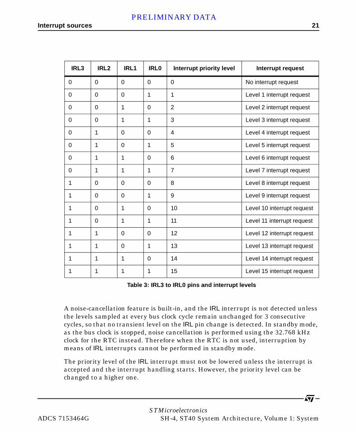
IRL interrupts are input by level at pins IRL3 to IRL0. The priority level is the level indicated by pins IRL3 to IRL0. An IRL3 to IRL0 value of 15 (1111) indicates the highest-level interrupt request (interrupt priority level 15). A value of 0 (0000) indicates no interrupt request (interrupt priority level 0). Figure 7 shows an examples of an IRL interrupt connection. Table 3 and Table 4 show IRL pins and interrupt levels.
Figure 7: Example of IRL interrupt connection
ST40…
Interrupt requests
Priority
encoder
4
IRL3 to IRL0
STMicroelectronicsSH-4, ST40 System Architecture, Volume 1: System ADCS 7153464G
Interrupt sources 21PRELIMINARY DATA
A noise-cancellation feature is built-in, and the IRL interrupt is not detected unless the levels sampled at every bus clock cycle remain unchanged for 3 consecutive cycles, so that no transient level on the IRL pin change is detected. In standby mode, as the bus clock is stopped, noise cancellation is performed using the 32.768 kHz clock for the RTC instead. Therefore when the RTC is not used, interruption by means of IRL interrupts cannot be performed in standby mode.
The priority level of the IRL interrupt must not be lowered unless the interrupt is accepted and the interrupt handling starts. However, the priority level can be changed to a higher one.
IRL3 IRL2 IRL1 IRL0 Interrupt priority level Interrupt request
0 0 0 0 0 No interrupt request
0 0 0 1 1 Level 1 interrupt request
0 0 1 0 2 Level 2 interrupt request
0 0 1 1 3 Level 3 interrupt request
0 1 0 0 4 Level 4 interrupt request
0 1 0 1 5 Level 5 interrupt request
0 1 1 0 6 Level 6 interrupt request
0 1 1 1 7 Level 7 interrupt request
1 0 0 0 8 Level 8 interrupt request
1 0 0 1 9 Level 9 interrupt request
1 0 1 0 10 Level 10 interrupt request
1 0 1 1 11 Level 11 interrupt request
1 1 0 0 12 Level 12 interrupt request
1 1 0 1 13 Level 13 interrupt request
1 1 1 0 14 Level 14 interrupt request
1 1 1 1 15 Level 15 interrupt request
Table 3: IRL3 to IRL0 pins and interrupt levels
STMicroelectronicsADCS 7153464G SH-4, ST40 System Architecture, Volume 1: System

22 Interrupt sourcesPRELIMINARY DATA
The interrupt mask bits (I3 to I0) in SR are not affected by IRL interrupt handling.
Setting the IRLM bit to 1 in the ICR register enables pins IRL0 to IRL3 to be used for 4 independent interrupt requests.
3.2.3 On-chip peripheral module interrupts
On-chip peripheral module interrupts are generated by the following core modules:
• timer unit (TMU),
• realtime clock (RTC),
• serial communication interfaces (SCIF1 and SCIF2),
• watchdog timer (WDT),
• UDI port.
Other modules integrated outside of the core also generate interrupts. These are detailed in the datasheet.
Not every interrupt source is assigned a different interrupt vector. Sources are reflected on the interrupt event register (INTEVT). It is easy to identify sources by using the values of INTEVT as branch offsets (in the exception handler routine).
The priority level (from 0 to 15) can be set for each module by writing to interrupt priority setting registers (IPRA to IPRD, INTPRI00).
The interrupt mask bits (I3 to I0) in SR are not affected by the on-chip peripheral module interrupt handling.
On-chip peripheral module interrupt source flag and interrupt enable flag updating should only be carried out when the BL bit in SR is set to 1. To prevent acceptance of an erroneous interrupt from an interrupt source that should have been updated, first read the on-chip peripheral register containing the relevant flag, then clear the BL bit to 0. This will secure the necessary timing internally. When updating a number of flags, there is no problem if only the register containing the last flag updated is read.
If flag updating is performed while the BL bit is cleared to 0, the program may jump to the interrupt service routine when the INTEVT register value is 0. In this case, interrupt handling is initiated due to the timing relationship between the flag update and interrupt request recognition within the chip. Processing can be continued without any problem by executing an RTE instruction.
STMicroelectronicsSH-4, ST40 System Architecture, Volume 1: System ADCS 7153464G
Interrupt sources 23PRELIMINARY DATA
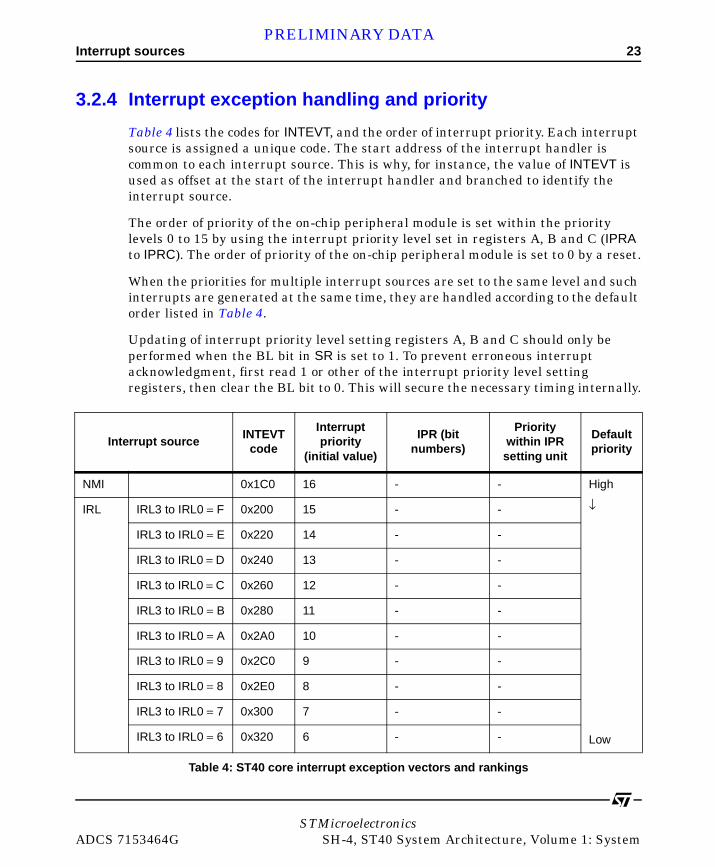
3.2.4 Interrupt exception handling and priority
Table 4 lists the codes for INTEVT, and the order of interrupt priority. Each interrupt source is assigned a unique code. The start address of the interrupt handler is common to each interrupt source. This is why, for instance, the value of INTEVT is used as offset at the start of the interrupt handler and branched to identify the interrupt source.
The order of priority of the on-chip peripheral module is set within the priority levels 0 to 15 by using the interrupt priority level set in registers A, B and C (IPRA to IPRC). The order of priority of the on-chip peripheral module is set to 0 by a reset.
When the priorities for multiple interrupt sources are set to the same level and such interrupts are generated at the same time, they are handled according to the default order listed in Table 4.
Updating of interrupt priority level setting registers A, B and C should only be performed when the BL bit in SR is set to 1. To prevent erroneous interrupt acknowledgment, first read 1 or other of the interrupt priority level setting registers, then clear the BL bit to 0. This will secure the necessary timing internally.
Interrupt sourceINTEVT
code
Interrupt priority
(initial value)
IPR (bit numbers)
Priority within IPR setting unit
Default priority
NMI 0x1C0 16 - - High
↓
Low
IRL IRL3 to IRL0 = F 0x200 15 - -
IRL3 to IRL0 = E 0x220 14 - -
IRL3 to IRL0 = D 0x240 13 - -
IRL3 to IRL0 = C 0x260 12 - -
IRL3 to IRL0 = B 0x280 11 - -
IRL3 to IRL0 = A 0x2A0 10 - -
IRL3 to IRL0 = 9 0x2C0 9 - -
IRL3 to IRL0 = 8 0x2E0 8 - -
IRL3 to IRL0 = 7 0x300 7 - -
IRL3 to IRL0 = 6 0x320 6 - -
Table 4: ST40 core interrupt exception vectors and rankings
STMicroelectronicsADCS 7153464G SH-4, ST40 System Architecture, Volume 1: System
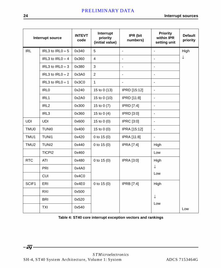
24 Interrupt sourcesPRELIMINARY DATA
IRL IRL3 to IRL0 = 5 0x340 5 - - High
↓
Low
IRL3 to IRL0 = 4 0x360 4 - -
IRL3 to IRL0 = 3 0x380 3 - -
IRL3 to IRL0 = 2 0x3A0 2 - -
IRL3 to IRL0 = 1 0x3C0 1 - -
IRL0 0x240 15 to 0 (13) IPRD [15:12] -
IRL1 0x2A0 15 to 0 (10) IPRD [11:8] -
IRL2 0x300 15 to 0 (7) IPRD [7:4] -
IRL3 0x360 15 to 0 (4) IPRD [3:0] -
UDI UDI 0x600 15 to 0 (0) IPRC [3:0] -
TMU0 TUNI0 0x400 15 to 0 (0) IPRA [15:12] -
TMU1 TUNI1 0x420 0 to 15 (0) IPRA [11:8] -
TMU2 TUNI2 0x440 0 to 15 (0) IPRA [7:4] High
TICPI2 0x460 Low
RTC ATI 0x480 0 to 15 (0) IPRA [3:0] High
↓
LowPRI 0x4A0
CUI 0x4C0
SCIF1 ERI 0x4E0 0 to 15 (0) IPRB [7:4] High
↓
Low
RXI 0x500
BRI 0x520
TXI 0x540
Interrupt sourceINTEVT
code
Interrupt priority
(initial value)
IPR (bit numbers)
Priority within IPR setting unit
Default priority
Table 4: ST40 core interrupt exception vectors and rankings
STMicroelectronicsSH-4, ST40 System Architecture, Volume 1: System ADCS 7153464G

Interrupt sources 25PRELIMINARY DATA
Further information about these interrupts is available elsewhere in this manual.
• TUNI0–TUNI2: Underflow interrupts, see Chapter 8: Timer unit (TMU) on page 227.
• TICPI2:Input capture interrupt, see Chapter 3: Interrupt controller (INTC) on page 15.
• ATI:Alarm interrupt, see Chapter 7: Real-time clock (RTC) on page 179.
• PRI:Periodic interrupt, see Chapter 7: Real-time clock (RTC) on page 179.
• CUI:Carry-up interrupt, Chapter 7: Real-time clock (RTC) on page 179.
• ERI:Receive error interrupt, see Chapter 9: Serial communication interface with FIFO (SCIF) on page 251.
• RXI:Receive-data-full interrupt, see Chapter 9: Serial communication interface with FIFO (SCIF) on page 251.
• TXI:Transmit-data-empty interrupt, see Chapter 9: Serial communication interface with FIFO (SCIF) on page 251.
• TEI:Transmit-data-end interrupt, see Chapter 9: Serial communication interface with FIFO (SCIF) on page 251.
• BRI:Break interrupt, see Chapter 9: Serial communication interface with FIFO (SCIF) on page 251.
• ITI:Interval timer interrupt, see Chapter 7: Real-time clock (RTC) on page 179.
SCIF2 ERI 0x700 0 to 15 (0) IPRC [7:4] High
↓
Low
High
↓
Low
RXI 0x720
BRI 0x740
TXI 0x760
WDT ITI 0x560 0 to 15 (0) IPRB [15:12] —
Other interrupts are device-specific and are listed in the datasheet.
Interrupt sourceINTEVT
code
Interrupt priority
(initial value)
IPR (bit numbers)
Priority within IPR setting unit
Default priority
Table 4: ST40 core interrupt exception vectors and rankings
STMicroelectronicsADCS 7153464G SH-4, ST40 System Architecture, Volume 1: System
26 INTC registersPRELIMINARY DATA
3.3 INTC registers
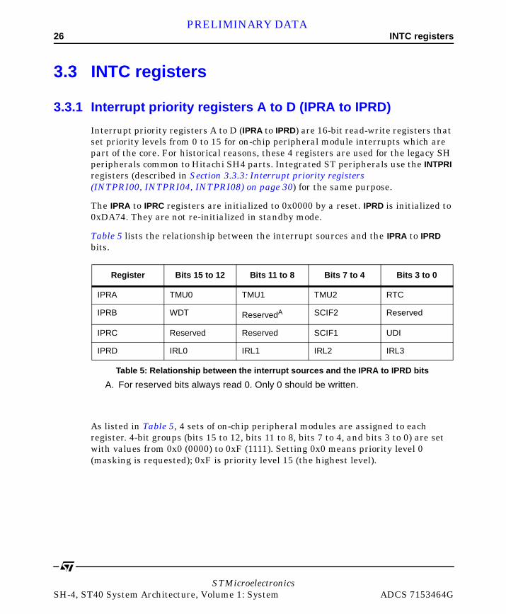
3.3.1 Interrupt priority registers A to D (IPRA to IPRD)
Interrupt priority registers A to D (IPRA to IPRD) are 16-bit read-write registers that set priority levels from 0 to 15 for on-chip peripheral module interrupts which are part of the core. For historical reasons, these 4 registers are used for the legacy SH peripherals common to Hitachi SH4 parts. Integrated ST peripherals use the INTPRI registers (described in Section 3.3.3: Interrupt priority registers (INTPRI00, INTPRI04, INTPRI08) on page 30) for the same purpose.
The IPRA to IPRC registers are initialized to 0x0000 by a reset. IPRD is initialized to 0xDA74. They are not re-initialized in standby mode.
Table 5 lists the relationship between the interrupt sources and the IPRA to IPRD bits.
As listed in Table 5, 4 sets of on-chip peripheral modules are assigned to each register. 4-bit groups (bits 15 to 12, bits 11 to 8, bits 7 to 4, and bits 3 to 0) are set with values from 0x0 (0000) to 0xF (1111). Setting 0x0 means priority level 0 (masking is requested); 0xF is priority level 15 (the highest level).
Register Bits 15 to 12 Bits 11 to 8 Bits 7 to 4 Bits 3 to 0
IPRA TMU0 TMU1 TMU2 RTC
IPRB WDT ReservedA
A. For reserved bits always read 0. Only 0 should be written.
SCIF2 Reserved
IPRC Reserved Reserved SCIF1 UDI
IPRD IRL0 IRL1 IRL2 IRL3
Table 5: Relationship between the interrupt sources and the IPRA to IPRD bits
STMicroelectronicsSH-4, ST40 System Architecture, Volume 1: System ADCS 7153464G

INTC registers 27PRELIMINARY DATA
3.3.2 Interrupt control register (ICR)
The interrupt control register (ICR) is a 16-bit register that sets the input signal detection mode for external interrupt input pin NMI and indicates the input signal level at the NMI pin. This register is initialized by a power-on reset or manual reset. It is not initialized in standby mode.
Bit 15: NMI input level (NMIL)
Sets the level of the signal input at the NMI pin. This bit can be read to determine the NMI pin level. It cannot be modified.
Bit: 15 14 13 12 11 10 9 8
Bit name NMIL MAI — — — — NMIB NMIE
Initial value 0/1 0 0 0 0 0 0 0
Type RO RW — — — — RW RW
Bit 7 6 5 4 3 2 1 0
Bit name IRLM — — — — — — —
Initial value 0 0 0 0 0 0 0 0
Type RW — — — — — — RW
Bit 15: NML Description
0 NMI input level is low.
1 NMI input level is high.
STMicroelectronicsADCS 7153464G SH-4, ST40 System Architecture, Volume 1: System

28 INTC registersPRELIMINARY DATA
Bit 14: NMI interrupt mask (MAI)
Specifies whether or not all interrupts are to be masked while the NMI pin input level is low, irrespective of the CPU’s SR.BL bit.
Bit 9: NMI block mode (NMIB)
Selects whether NMI requests are held pending or immediately detected when the SR.BL bit is 1.
Bit 8: NMI edge select (NMIE)
Selects whether the falling or rising edge of the interrupt request signal to the NMI is detected.
Bit 14: MAI Description
0 Interrupts are enabled even while NMI pin is low (initial value).
1 Interrupts are disabled while NMI pin is lowA.
A. NMI interrupts are accepted in normal operation and in sleep mode. In standby mode, all interrupts are masked, and standby is not cleared, while the NMI pin is low.
Bit 9: NMIB DescriptionA
A. If an interrupt request is accepted while SR.BL = 1, the previous exception information will be lost, and so should be saved beforehand.This bit is cleared automatically when an NMI interrupt is accepted.
0 NMI interrupt requests are held pending when SR.BL = 1 (initial value).
1 NMI interrupt requests are detected when SR.BL = 1.
Bit 8: NMIE Description
0 An interrupt request is detected on the falling edge of NMI input (initial value).
1 An interrupt request is detected on the rising edge of NMI input.
STMicroelectronicsSH-4, ST40 System Architecture, Volume 1: System ADCS 7153464G

INTC registers 29PRELIMINARY DATA
Bit 7: IRL pin mode
Selects whether pins IRL3 to IRL0 are used for level-encoded interrupt requests or for 4 independent interrupt requests.
Bits 13 to 10 and 6 to 0: reserved
These bits are always read as 0, and should only be written with 0.
Bit 7: IRLM Description
0 IRL pins are used for level-encoded interrupt requests (initial value).
1 IRL pins are used for 4 independent interrupt requests.
STMicroelectronicsADCS 7153464G SH-4, ST40 System Architecture, Volume 1: System
30 INTC registersPRELIMINARY DATA
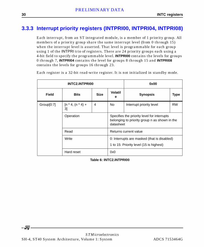
3.3.3 Interrupt priority registers (INTPRI00, INTPRI04, INTPRI08)
Each interrupt, from an ST integrated module, is a member of 1 priority group. All members of a priority group share the same interrupt level (from 0 through 15) when the interrupt level is asserted. That level is programmable for each group using 1 of the INTPRI trio of registers. There are 24 priority groups each using a 4-bit field to specify the programmable level. INTPRI00 contains the levels for groups 0 through 7, INTPRI04 contains the level for groups 8 through 15 and INTPRI08 contains the levels for groups 16 through 23.
Each register is a 32-bit read-write register. It is not initialized in standby mode.
INTC2.INTPRI00 0x00
Field Bits SizeVolatil
eSynopsis Type
Group[0:7] [n * 4, (n * 4) + 3]
4 No Interrupt priority level RW
Operation Specifies the priority level for interrupts belonging to priority group n as shown in the datasheet
Read Returns current value
Write 0: Interrupts are masked (that is disabled)
1 to 15: Priority level (15 is highest)
Hard reset 0x0
Table 6: INTC2.INTPRI00
STMicroelectronicsSH-4, ST40 System Architecture, Volume 1: System ADCS 7153464G

INTC registers 31PRELIMINARY DATA
INTC2.INTPRI04 0x04
Field Bits SizeVolatil
eSynopsis Type
Group[8:15] [(n - 8) * 4, ((n - 8) * 4) + 3]
4 No Interrupt priority level RW
Operation Specifies the priority level for interrupts belonging to priority group[n] as shown in the datasheet
Read Returns current value
Write 0: Interrupts are masked (that is disabled)
1 to 15: Priority level (15 is highest)
Hard reset 0x0
Table 7: INTC2.INTPRI04
INTC2.INTPRI08 0x08
Field Bits SizeVolatil
eSynopsis Type
Group[16:23] [(n -16) * 4, ((n - 16) * 4) + 3]
4 No Interrupt priority level RW
Operation Specifies the priority level for interrupts belonging to priority group[n] as shown in the datasheet
Read Returns current value
Write 0: Interrupts are masked (that is disabled)
1 to 15: Priority level (15 is highest)
Hard reset 0x0
Table 8: INTC2.INTPRI08
STMicroelectronicsADCS 7153464G SH-4, ST40 System Architecture, Volume 1: System

32 INTC registersPRELIMINARY DATA
3.3.4 Interrupt request registers (INTREQ00, INTREQ04, INTREQ08)
The interrupt request registers are 32-bit registers that show which of the interrupts arising from ST integrated modules have been asserted. Regardless of the state of the INTPRI and INTMSK registers the INTREQ registers will indicate all asserted interrupts. The association between bits in the INTREQ registers and interrupts is given in the data sheet for each particular device.
The architecture supports up to 96 ST integrated interrupts. Unused bits are reserved. These bits always read as 0 and writes to them are ignored.
INTC2.INTREQ00 0x20
Field Bits Size Volatile Synopsis Type
IR[0:31] [0:31] 1 Yes Interrupt request level RO
Operation Indicates the request level of the interrupt associated with bit[n], with associations between bits and interrupts being defined in the datasheet for the device
Read 0: Interrupt not being asserted
1: Interrupt being asserted
Write Invalid
Hard reset 0
Table 9: IINTC2.NTREQ00
STMicroelectronicsSH-4, ST40 System Architecture, Volume 1: System ADCS 7153464G

INTC registers 33PRELIMINARY DATA
INTC2.INTREQ04 0x24
Field Bits Size Volatile Synopsis Type
IR[32:63] [32:63] 1 Yes Interrupt request level RO
Operation Indicates the request level of the interrupt associated with bit[n], with associations between bits and interrupts being defined in the datasheet
Read 0: Interrupt not being asserted
1: Interrupt being asserted
Write Invalid
Hard reset 0
Table 10: INTC2.INTREQ04
INTC2.INTREQ08 0x28
Field Bits Size Volatile Synopsis Type
IR[64:95] [64:95] 1 Yes Interrupt request level RO
Operation Indicates the request level of the interrupt associated with bit[n], with associations between bits and interrupts being defined in the datasheet
Read 0: Interrupt not being asserted
1: Interrupt being asserted
Write Invalid
Hard reset 0
Table 11: INTC2.INTREQ08
STMicroelectronicsADCS 7153464G SH-4, ST40 System Architecture, Volume 1: System
34 INTC registersPRELIMINARY DATA
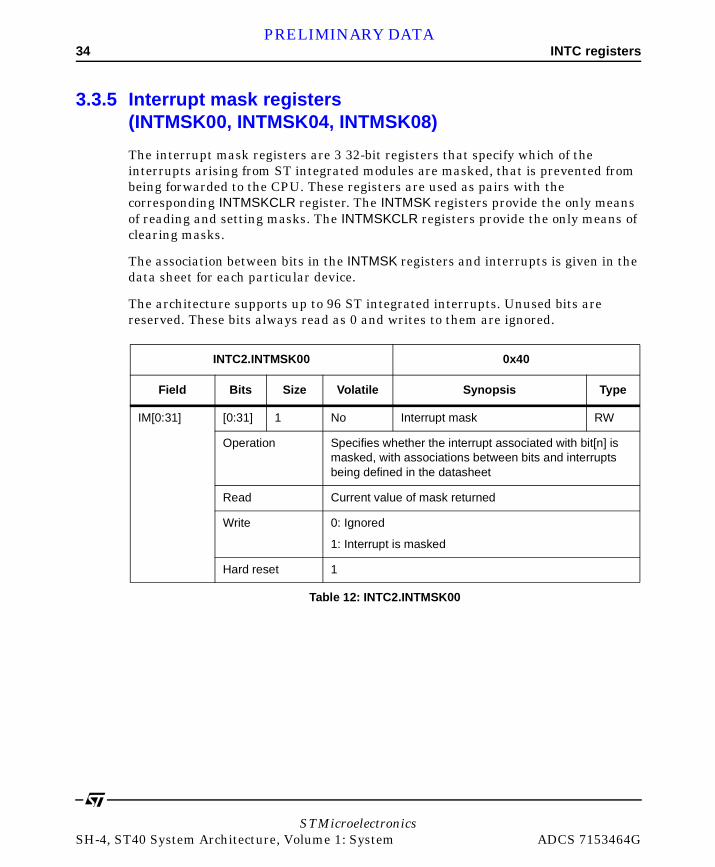
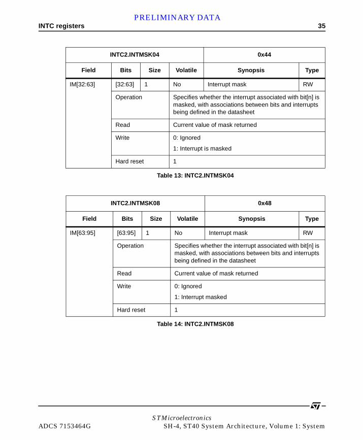
3.3.5 Interrupt mask registers (INTMSK00, INTMSK04, INTMSK08)
The interrupt mask registers are 3 32-bit registers that specify which of the interrupts arising from ST integrated modules are masked, that is prevented from being forwarded to the CPU. These registers are used as pairs with the corresponding INTMSKCLR register. The INTMSK registers provide the only means of reading and setting masks. The INTMSKCLR registers provide the only means of clearing masks.
The association between bits in the INTMSK registers and interrupts is given in the data sheet for each particular device.
The architecture supports up to 96 ST integrated interrupts. Unused bits are reserved. These bits always read as 0 and writes to them are ignored.
INTC2.INTMSK00 0x40
Field Bits Size Volatile Synopsis Type
IM[0:31] [0:31] 1 No Interrupt mask RW
Operation Specifies whether the interrupt associated with bit[n] is masked, with associations between bits and interrupts being defined in the datasheet
Read Current value of mask returned
Write 0: Ignored
1: Interrupt is masked
Hard reset 1
Table 12: INTC2.INTMSK00
STMicroelectronicsSH-4, ST40 System Architecture, Volume 1: System ADCS 7153464G
INTC registers 35PRELIMINARY DATA
INTC2.INTMSK04 0x44
Field Bits Size Volatile Synopsis Type
IM[32:63] [32:63] 1 No Interrupt mask RW
Operation Specifies whether the interrupt associated with bit[n] is masked, with associations between bits and interrupts being defined in the datasheet
Read Current value of mask returned
Write 0: Ignored
1: Interrupt is masked
Hard reset 1
Table 13: INTC2.INTMSK04
INTC2.INTMSK08 0x48
Field Bits Size Volatile Synopsis Type
IM[63:95] [63:95] 1 No Interrupt mask RW
Operation Specifies whether the interrupt associated with bit[n] is masked, with associations between bits and interrupts being defined in the datasheet
Read Current value of mask returned
Write 0: Ignored
1: Interrupt masked
Hard reset 1
Table 14: INTC2.INTMSK08
STMicroelectronicsADCS 7153464G SH-4, ST40 System Architecture, Volume 1: System
36 INTC registersPRELIMINARY DATA
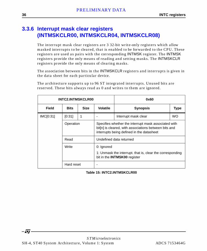
3.3.6 Interrupt mask clear registers (INTMSKCLR00, INTMSKCLR04, INTMSKCLR08)
The interrupt mask clear registers are 3 32-bit write-only registers which allow masked interrupts to be cleared, that is enabled to be forwarded to the CPU. These registers are used as pairs with the corresponding INTMSK register. The INTMSK registers provide the only means of reading and setting masks. The INTMSKCLR registers provide the only means of clearing masks.
The association between bits in the INTMSKCLR registers and interrupts is given in the data sheet for each particular device.
The architecture supports up to 96 ST integrated interrupts. Unused bits are reserved. These bits always read as 0 and writes to them are ignored.
INTC2.INTMSKCLR00 0x60
Field Bits Size Volatile Synopsis Type
IMC[0:31] [0:31] 1 - Interrupt mask clear WO
Operation Specifies whether the interrupt mask associated with bit[n] is cleared, with associations between bits and interrupts being defined in the datasheet
Read Undefined data returned
Write 0: Ignored
1: Unmask the interrupt. that is, clear the corresponding bit in the INTMSK00 register
Hard reset -
Table 15: INTC2.INTMSKCLR00
STMicroelectronicsSH-4, ST40 System Architecture, Volume 1: System ADCS 7153464G

INTC registers 37PRELIMINARY DATA
INTC2.INTMSKCLR04 0x64
Field Bits Size Volatile Synopsis Type
IMC[32:63] [32:63] 1 - Interrupt mask clear WO
Operation Specifies whether the interrupt mask associated with bit j-32 is cleared, with associations between bits and interrupts being defined in the datasheet
Read Undefined data returned
Write 0: Ignored
1: Unmask the interrupt. that is, clear the corresponding bit in the INTMSK04 register
Hard reset -
Table 16: INTC2.INTMSKCLR04
INTC2.INTMSKCLR08 0x68
Field Bits Size Volatile Synopsis Type
IMC[64:95] [64:95] 1 - Interrupt mask clear WO
Operation Specifies whether the interrupt mask associated with bit[n] is cleared, with associations between bits and interrupts being defined in the datasheet
Read Undefined data returned
Write 0: Ignored
1: Unmask the interrupt that is, clear the corresponding bit in the INTMSK08 register
Hard reset -
Table 17: INTC2.INTMSKCLR08
STMicroelectronicsADCS 7153464G SH-4, ST40 System Architecture, Volume 1: System
38 INTC registersPRELIMINARY DATA
3.3.7 INTC2 mode register (INTC2MODE)
The INTC2MODE register is a 32-bit read-write register which is used to restrict the INTEVT code range of the interrupts arising from ST modules. These modules are listed in Table 5: Relationship between the interrupt sources and the IPRA to IPRD bits on page 26. The effect of this restriction is to map all interrupts arising from ST modules onto the same INTEVT codes used by the IRL interrupts as shown in Table 12: INTC2.INTMSK00 on page 34. For example the interrupt having code listed as 0xA00 in Table 4: ST40 core interrupt exception vectors and rankings on page 23 will generate code 0x200 when INTC2MODE.FLAG = 1, and will generate code 0xA00 otherwise.
This register allows ST40 devices to circumvent problems with legacy software which do not handle INTEVT codes which have their top bit set1. In such cases software interrupt service routines have the responsibility to disambiguate interrupts using codes in the IRL range by, among other things, inspecting the INTREQ registers.
1. At the time of writing such legacy software include the WinCE 2.12 operating system.
STMicroelectronicsSH-4, ST40 System Architecture, Volume 1: System ADCS 7153464G

INTC registers 39PRELIMINARY DATA
INTC2.INTC2MODE 0x80
Field Bits Size Volatile Synopsis Type
FLAG 0 1 No INTC2MODE register RW
Operation Specifies whether the range of INTEVT codes passed to the CPU are modified with respect to the values in Table 4: ST40 core interrupt exception vectors and rankings on page 23
Read Returns current data
Write 0: INTEVT code unmodified
1: Top 3 bits of the INTEVT codes for ST modules replaced with 0b’001 before being passed to the CPU
Hard reset 0
[1:31] 31 - Reserved R
Operation Reserved field
Read Undefined
Write 0
Hard reset Undefined
Table 18: INTC2.INTC2MODE
STMicroelectronicsADCS 7153464G SH-4, ST40 System Architecture, Volume 1: System

40 INTC operationPRELIMINARY DATA
3.4 INTC operation
3.4.1 Interrupt sequence
The sequence of interrupt operations is explained below. Figure 8 is a flowchart of the operations.
1 The interrupt request sources send interrupt request signals to the interrupt controller.
2 The interrupt controller selects the highest priority interrupt from the interrupt requests sent, according to the priority levels set in interrupt priority registers A to C (IPRA to IPRC) and the INTPRI registers. Lower priority interrupts are held pending. If 2 of these interrupts have the same priority level or if multiple interrupts occur within a single module, the interrupt with the highest default priority or the highest priority within its IPR setting unit (as indicated in Figure 8) is selected.
3 The priority level of the interrupt selected by the interrupt controller is compared with the interrupt mask bits (I3 to I0) in SR of the CPU. If the request priority level is higher than the level in bits I3–I0, the interrupt controller accepts the interrupt and sends an interrupt request signal to the CPU.
4 The CPU receives an interrupt at a break in instructions.
5 The interrupt source code is set in INTEVT.
6 SR and program counter (PC) are saved to SSR and SPC, respectively.
7 The block bit (BL), mode bit (MD), and register bank bit (RB) in SR are set to 1.
8 The CPU jumps to the start address of the interrupt handler (the sum of the value set in the vector base register (VBR) and 0x00000600). The interrupt handler may branch with the INTEVT register value as it is offset in order to identify the interrupt source. This enables it to branch to the handling routine for the individual interrupt source.
Note: 1 The interrupt mask bits (I3 to I0) in SR are not changed by acceptance of an interrupt in the CPU.
The interrupt source flag should be cleared in the interrupt handler. To ensure that an interrupt request that should have been cleared is not inadvertently accepted again, read the interrupt source flag after it has been cleared, then wait for the interval shown in Table 19.6 (Time for priority decision and SR mask bit comparison) before clearing the BL bit or executing an RTE instruction.
STMicroelectronicsSH-4, ST40 System Architecture, Volume 1: System ADCS 7153464G

INTC operation 41PRELIMINARY DATA
Note: *I3-I0: Interrupt mask bits in status register (SR)
Figure 8: Interrupt operation flowchart
Program execution state
(BL bitin SR=0) or
(sleep or standbymode)?
Interruptgenerated?
NMI?
Set interrupt sourcein INTEVT
Save SR to SSR;save PC to SPC
Set BL, MD, RB bitsin SR to 1
Branch to exceptionhandler
NMIB inICR=1 andNMI?
Level 15interrupt?
I3-I0*=level 14 or
lower?
Level 14interrupt?
I3-I0*=level 13 or
lower?
I3-I0*=level 0?
Level 0interrupt?
No
No
No
No
No
No
No
No
No
No
Yes
Yes
Yes
Yes
Yes
Yes
Yes
Yes
Yes
STMicroelectronicsADCS 7153464G SH-4, ST40 System Architecture, Volume 1: System
42 INTC operationPRELIMINARY DATA
3.4.2 Multiple interrupts
When handling multiple interrupts, an interrupt handler should include the procedure below.
1 Branch to a specific interrupt handler corresponding to a code set in INTEVT. The code in INTEVT can be used as a branch-offset for branching to the specific handler.
2 Clear the cause of the interrupt in each specific handler.
3 Save SSR and SPC to memory.
4 Clear the BL bit in SR, and set the accepted interrupt level in the interrupt mask bits in SR.
5 Handle the interrupt.
6 Set the BL bit in SR to 1.
7 Return the SSR and SPC from memory.
8 Execute the RTE instruction.
When this procedure is followed in order, an interrupt of higher priority than the 1 being handled can be accepted after clearing BL in step 4. Figure 8 shows a sample interrupt operation flowchart.
STMicroelectronicsSH-4, ST40 System Architecture, Volume 1: System ADCS 7153464G

PRELIMINARY DATA
STMicroelectroniADCS 7153464G SH-4, ST40 S
4
GPDMA controller (DMAC)This design includes a sophisticated on-chip five channel general purpose direct memory access controller (DMAC). The DMAC can be used in place of the CPU to perform low-impact high-performance data transfers between memory-mapped device modules and memory, and perform high performance memory-to-memory moves.
4.1 FeaturesThe DMAC has the following features:
• 5 independent dual address DMA channels,
• transfer of information to and from aligned or unaligned data structures of up to 4 Gbytes in the following organizations:
- single location (0D),
- incrementing or decrementing linear arrays (1D),
- incrementing or decrementing rectangular arrays (2D),
• transfer units of 1,2,4,8,16 or 32 bytes,
• triggered1, paced2 or auto-request timing models,
1. A channel is triggered if an external request causes a complete DMA operation to start and complete after 1 or more data units are transferred.
2. A channel is paced if an external request causes a single data unit to be transferred per request. The DMAC may require multiple requests to complete the operation.
csystem Architecture, Volume 1: System

44 FeaturesPRELIMINARY DATA
• support for up to 32 request-generating peripherals1,
• support for 2 interrupt models,
- a single interrupt per DMA channel which signals normal completion on each channel plus a shared error interrupt which signals abnormal completion,
- a single interrupt per DMA channel which signals both normal and abnormal completion on each channel,
• transparent support for both little and big endian data organisations.2
Channel 0 additionally supports multiplexing of up to 32 simultaneously active subchannels on to a single physical channel. Each DMA subchannel is associated with a specific peripheral and defined by a copy of its register state which is stored in main memory.
Channels 1 to 4 additionally allow a series of independent DMA operations to be stored in memory as a linked list. This allows each DMA channel to sequence a set of DMA transfers and allow complex operations such as scatter-gather to be achieved without requiring CPU intervention.
1. A request is a communication between a peripheral and a DMA channel, and is used to trigger or pace movement of data on that channel.
2. The DMAC always uses the same data organisation as the CPU and can be considered as an endian-independent device by software. The endian model used is determined statically following reset.
STMicroelectronicsSH-4, ST40 System Architecture, Volume 1: System ADCS 7153464G

Address map 45PRELIMINARY DATA
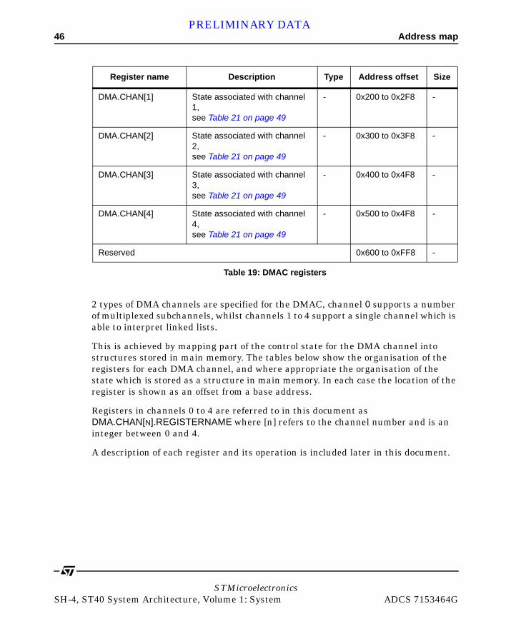
4.2 Address mapThe DMAC address map is organized into 2 regions. The first region is associated with global control and status information, the second with DMA channel-specific information. This second region is divided into a number of independent areas, each area containing control and status information specific to the physical DMA channel.
Register name Description Type Address offset Size
DMA.VCR.STATUS Version control register: module status, see Table 22 on page 62
RW 0x00 32
DMA.VCR.VERSION Version control register: module version, see Table 23 on page 64
RO 0x08 32
DMA.ENABLE Global enable,see Table 24 on page 65
RW 0x10 32
DMA.DISABLE Global disable, see Table 25 on page 66
WO 0x18 32
DMA.STATUS Global DMA status, see Table 26 on page 67
RO 0x20 32
DMA.INTERRUPT Global interrupt status, see Table 27 on page 68
RO 0x28 32
DMA.ERROR Global error status, see Table 28 on page 69
RO 0x30 32
DMA.DEFINED Global DMA channel defined, see Table 29 on page 70
RO 0x38 32
DMA.HANDSHAKE Global request handshake protocol, see Table 30 on page 70
RW 0x40 32
Reserved 0x40 to 0xF8 -
DMA.CHAN[0] State associated with channel 0, see Table 20 on page 47
- 0x100 to 0x1F8 -
Table 19: DMAC registers
STMicroelectronicsADCS 7153464G SH-4, ST40 System Architecture, Volume 1: System
46 Address mapPRELIMINARY DATA
2 types of DMA channels are specified for the DMAC, channel 0 supports a number of multiplexed subchannels, whilst channels 1 to 4 support a single channel which is able to interpret linked lists.
This is achieved by mapping part of the control state for the DMA channel into structures stored in main memory. The tables below show the organisation of the registers for each DMA channel, and where appropriate the organisation of the state which is stored as a structure in main memory. In each case the location of the register is shown as an offset from a base address.
Registers in channels 0 to 4 are referred to in this document as DMA.CHAN[N].REGISTERNAME where [n] refers to the channel number and is an integer between 0 and 4.
A description of each register and its operation is included later in this document.
DMA.CHAN[1] State associated with channel 1, see Table 21 on page 49
- 0x200 to 0x2F8 -
DMA.CHAN[2] State associated with channel 2, see Table 21 on page 49
- 0x300 to 0x3F8 -
DMA.CHAN[3] State associated with channel 3, see Table 21 on page 49
- 0x400 to 0x4F8 -
DMA.CHAN[4] State associated with channel 4, see Table 21 on page 49
- 0x500 to 0x4F8 -
Reserved 0x600 to 0xFF8 -
Register name Description Type Address offset Size
Table 19: DMAC registers
STMicroelectronicsSH-4, ST40 System Architecture, Volume 1: System ADCS 7153464G

Address map 47PRELIMINARY DATA
4.2.1 Channel 0: multiplexed DMA channel
Register name
Description TypeAddress
offset Memory
offset Access
size
IDENTITY Local state
Channel identity, see Table 31 on page 71
RO 0x00 - 32
ENABLE Enable a control bit associated with this channel, see Table 32 on page 75
RW 0x08 - 32
DISABLE Disable a control bit associated with this channel, see Table 33 on page 77
WO 0x10 - 32
STATUS Status of a control bit associated with this channel, see Table 34 on page 80
RW 0x18 - 32
ACTION Cause action on a control bit associated with this channel, see Table 35 on page 83
WO 0x20 - 32
POINTER Pointer to the current or last register memory image, see Table 36 on page 85
RO 0x28 - 32
SUBBASE Base pointer to the table of register images in main memory, see Table 38 on page 88
RW 0x30 - 32
SUBENABLE Subchannel enable, see Table 39 on page 89
RW 0x38 - 32
SUBDISABLE Subchannel disable, see Table 40 on page 90
WO 0x40 - 32
SUBINT_ENB Subchannel interrupt enable, see Table 41 on page 90
RW 0x48 - 32
SUBINT_DIS Subchannel interrupt disable, see Table 42 on page 91
WO 0x50 - 32
Table 20: Channel 0 registers
STMicroelectronicsADCS 7153464G SH-4, ST40 System Architecture, Volume 1: System

48 Address mapPRELIMINARY DATA
SUBINT_STAT Local state
Subchannel interrupt status, see Table 43 on page 91
RO 0x58 - 32
Reserved 0x70 to 0x78
SUBINT_ACT Subchannel interrupt action, see Table 44 on page 92
WO 0x60 - 32
CONTROL Memory mapped state
Channel control, Table 45 on page 93
RW 0x80 0x00 32
COUNT Channel count, see Table 46 on page 99
RW 0x88 0x04 32
SAR Channel source address, see Table 47 on page 100
RW 0x90 0x08 32
DAR Channel destination address, see Table 48 on page 101
RW 0x98 0x0c 32
Reserved 0x60 to 0xf8
- -
Register name
Description TypeAddress
offset Memory
offset Access
size
Table 20: Channel 0 registers
STMicroelectronicsSH-4, ST40 System Architecture, Volume 1: System ADCS 7153464G

Address map 49PRELIMINARY DATA
4.2.2 Channels 1 to 4: linked list DMA channel
Register name Description TypeRegister
offset Memory offset
Size
IDENTITY Local state
Channel identity, seeTable 31 on page 71
RO 0x00 - 32
ENABLE Enable or set a control bit associated with this channel, seeTable 32 on page 75
RW 0x08 - 32
DISABLE Disable or reset a control bit associated with this channel, see Table 33 on page 77
WO 0x10 - 32
STATUS Status of a control bit associated with this channel, see Table 34 on page 80
RW 0x18 - 32
ACTION Cause action on a control bit associated with this channel, see Table 35 on page 83
WO 0x20 - 32
POINTER Pointer to the current or last register set, see Table 36 on page 85
RO 0x28 - 32
REQUEST The number of the request associated with this channel, see Table 37 on page 86
RW 0x30 - 32
Reserved 0x38 to 0x78
- -
CONTROL Memory mapped state
Channel control, see Table 45 on page 93
RW 0x80 0x00 32
COUNT Channel count, see Table 46 on page 99
RW 0x88 0x04 32
SAR Channel source address, see Table 47 on page 100
RW 0x90 0x08 32
Table 21: Channels 1 to 4 registers
STMicroelectronicsADCS 7153464G SH-4, ST40 System Architecture, Volume 1: System

50 Peripheral allocationPRELIMINARY DATA
4.3 Peripheral allocationThe DMAC supports up to 32 independent request sources. The peripheral to request number allocation is described in the relevant product datasheet.
The user may associate any request number with a specific DMA channel by programming the associated control state. This association is automatic for channel 0 and can be set by programming DMA.CHAN[N].REQUEST for channels 1 to 4.
DAR Memory mapped state
Channel destination address, see Table 48 on page 101
RW 0x98 0x0c 32
NEXT_PTR Pointer to the next register set, see Table 49 on page 102
RW 0xA0 0x10 32
SRC_LENGTH 2D source line length, see Table 50 on page 103
RW 0xA8 0x14 32
SRC_STRIDE 2D source line stride, see Table 51 on page 104
RW 0xB0 0x18 32
DST_LENGTH 2D destination line length, see Table 52 on page 105
RW 0xB8 0x1c 32
DST_STRIDE 2D destination line stride, see Table 53 on page 106
RW 0xC0 0x20 32
Reserved 0xC8 to 0xF8
- -
Register name Description TypeRegister
offset Memory offset
Size
Table 21: Channels 1 to 4 registers
STMicroelectronicsSH-4, ST40 System Architecture, Volume 1: System ADCS 7153464G
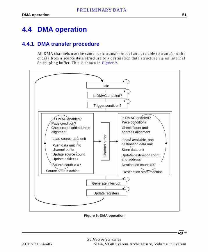
DMA operation 51PRELIMINARY DATA
4.4 DMA operation
4.4.1 DMA transfer procedure
All DMA channels use the same basic transfer model and are able to transfer units of data from a source data structure to a destination data structure via an internal de-coupling buffer. This is shown in Figure 9.
Figure 9: DMA operation
Idle
Is DMAC enabled?
Generate interrupt
Update registers
Is DMAC enabled?
Check count and address alignment
Load source data unit
Push data unit into channel bufferUpdate source count, Update address
Source count ≠ 0?
Is DMAC enabled?
Check count and address alignment
Store data unit
If data available, pop destination data unit
Update destination count, and address
Destination count ≠0?
Destination state machineSource state machine
Cha
nnel
buf
fer
Trigger condition?
Pace condition? Pace condition?
STMicroelectronicsADCS 7153464G SH-4, ST40 System Architecture, Volume 1: System

52 DMA operationPRELIMINARY DATA
The DMA operation is begun when all registers associated with the channel are programmed, and all enables associated with that channel are set.
Depending on the timing model associated with the DMA channel, the transfer may self-start or wait for a peripheral to assert a request before commencing a transfer.
The transfer of data occurs from a source memory structure to a destination memory structure via an internal de-coupling buffer using a specified data unit size. As the source and destination unit sizes may differ the DMAC may be required to load multiple units from the source for every destination unit or vice-versa.
A transfer will continue until 1 of the following conditions occurs.
Stall
When a stall condition occurs the register DMA.CHAN[N].ENABLE.STALL is set. All transfers on this channel are suspended until the stall condition is cleared and software has reset the DMA.CHAN[N].CONTROL.STALL.
Error
An error may occur if the DMAC attempts an access which is unalignable with the specified transfer unit (address or unit size) with alignment checks enabled or the system indicates that a memory operation has failed. This will force the DMA channel to stop until the error is cleared and the DMA channel reprogrammed.
Disable
The channel may be disabled at any time by a write to DMA.DISABLE[N], DMA.CHAN[N].DISABLE. The channel will be stopped until re-enabled by a second write to DMA.ENABLE or DMA.CHAN[N].ENABLE.
Completion
Completion occurs when DMA.CHAN[N].COUNT reaches 0, and the last transfer has completed. On completion the DMAC may interrupt the CPU or trigger an update function refreshing the DMA register state from memory and starting a subsequent transfer.
If an interrupt occurs the CPU is required to intervene before the DMA may continue or a further DMA begin on the same channel.
STMicroelectronicsSH-4, ST40 System Architecture, Volume 1: System ADCS 7153464G
DMA operation 53PRELIMINARY DATA
4.4.2 DMA transfer units
The DMAC is able to transfer data between the source and destination using units of specific size. Supported unit sizes include 1, 2, 4, 8 16 or 32 bytes. This is defined as the SRC_UNIT and DST_UNIT fields of in the DMA.CHAN[N].CONTROL registers for linked list channels, and SRC_UNIT for channel 0.
All transfers are aligned and of a specific size, the DMAC will not generate part word accesses. If the transfer if not alignable to the selected transfer unit, the DMAC will either indicate an alignment error or use the largest alignable transfer unit equal to or smaller than the selected unit.
If the alignment error interrupt is enabled the channel will be stalled until the error condition is cleared. This is indicated by asserting the associated error and setting the bits with the DMA.VCR.STATUS and DMA.ERROR registers.
As channels 1 to 4 support differing unit sizes for the source and destination structures, the DMA channel will segment and assemble the appropriate number of smaller data units to allow the larger unit to be transferred. Channel 0 will use the same transfer unit for both the source and destination transfers.
4.4.3 DMA timing model
The DMAC is able support 3 timing modes. This is selected for each channel by asserting the appropriate value into the DMA.CHAN[N].CONTROL.TIMING register. These are described below.
Free-running
If a channel is free-running, the DMA will occur without requiring a request to begin or control the timing of the transfer. It will continue to operate without further intervention until disabled, complete or an abnormal condition occurs.
This is the model generally used for memory-to-memory moves.
Triggered
A channel is triggered, if a request is required to start the DMA operation. Following the triggering request the DMA continues as if it were free-running until disabled, complete or an abnormal condition occurs.
This is typically used to communicate between devices, or start a memory-to- memory transfer which needs to be dependent on an external request.
STMicroelectronicsADCS 7153464G SH-4, ST40 System Architecture, Volume 1: System

54 DMA operationPRELIMINARY DATA
Paced
A channel is paced, if a single data unit is transferred per request. The request may be associated with either the source or destination memory location. The size of the data unit to be transferred is determined by the information associated with the source if the transfer is source-paced, and the destination if the transfer is destination-paced.
This is typically used by peripheral modules which require low data rate transfers such as UARTs.
4.4.4 DMA requests
The DMAC supports up to 32 physical request channels which may be used to trigger or pace any DMA channel. The association between the DMA channel and request is defined by the DMA.CHAN[N].REQUEST and DMA.CHAN[N].SUBCHAN_ENB registers and allows 1 request to be associated with 1 DMA channel or subchannel.
2 request protocols are supported:
• DREQ,
• DREQ/DRACK.
The first protocol uses the SuperHyway response to determine when a DMA unit (if paced) or complete DMA (if triggered) transfer has completed. This is assumed to be the cycle the final response packet received plus an offset period. The DMAC is able to begin sampling for the request pending the next transfer after this period.
The second protocol uses the DRACK signal to determine that the device has committed to a transfer, may re-sample the DREQ signal when the offset has passed following the acknowledgment.
Devices which support DRACK may choose to improve the efficiency of the DMA transfer to that device by reasserting req before the current data transfer to that device has completed allowing pipelining of multiple data units.
Each request associated with a peripheral is independent and may be mapped onto any DMA channel, and therefore more than 1 request may occur in a single cycle, or a single request may be mapped onto multiple DMA channels.
If a request is associated with multiple DMA channels, the request will be serviced by the lowest numbered channel, which means channel[n] has priority over channel[n + 1]. If multiple requests are associated with a single DMA channel
STMicroelectronicsSH-4, ST40 System Architecture, Volume 1: System ADCS 7153464G
DMA operation 55PRELIMINARY DATA
(channel 0) then the lowest number request will be serviced first, that is request[n] has priority over request[n + 1].
4.4.5 DMA data organization
The DMA is able to transfer data which is organized in a number of different ways. These include:
• single location (0D),
• incrementing or decrementing linear arrays (1D),
• incrementing or decrementing rectangular arrays (2D).
The data organization for the source and destination structures is defined by DMA.CHAN[N].CONTROL.SRC_TYPE, and DMA.CHAN[N].CONTROL.DST_TYPE respectively.
All data structures are specified with respect to an origin or initial byte address and the address of subsequent transfers is calculated from this origin using the information defined for that channel.
Single location/0D
If the data structure is fixed or single location, the same address is used throughout the transfer and no further information is needed.
Incrementing/1D
If the data structure is 1D, this address is incremented or decremented by the number of bytes in the data transfer unit until DMA.CHAN[N].COUNT bytes are transferred.
In an incrementing transfer from address ADDR of COUNT bytes, the following bytes at the following addresses will be transferred:
ADDR to ADDR + (COUNT - 1).
In a decremented transfer from address ADDR of COUNT bytes, the following bytes at the following addresses will be transferred:
ADDR to ADDR - (COUNT - 1).
STMicroelectronicsADCS 7153464G SH-4, ST40 System Architecture, Volume 1: System

56 DMA operationPRELIMINARY DATA
Rectangular array/2D
If the data structure is 2D, 2 additional parameters are defined, LENGTH and STRIDE. The transfer may be considered as a series of line or 1D transfers each of length bytes, each line separated by STRIDE - LENGTH bytes of unused data.
In the case of an incrementing structure the address defines the bottom left corner (lowest address), and the DMA transfers a series of data units, first transferring a line containing LENGTH bytes, before incrementing the address by STRIDE bytes and continuing for the next line. This operation is repeated until the required number of bytes is transferred. For a decrementing structure, the address defines the top right corner (highest address), and all addresses are decremented.
The bytes transferred for an incrementing transfer as follows:
IF (COUNT - total number of bytes transfer) > LENGTH, transfer the bytes at addresses:
ADDR to (ADDR + LENGTH - 1)
(ADDR + STRIDE) to (ADDR + STRIDE + LENGTH - 1)
....
(ADDR + (n - 1) * STRIDE) to (ADDR + (n - 1) * STRIDE + LENGTH - 1)
UNTIL (COUNT - total number of bytes transferred) <= LENGTH, transfer the bytes at addresses:
(ADDR + n * STRIDE) to (ADDR + n * STRIDE + (COUNT - number of bytes transferred))
The transfer is now completed.
The bytes transferred during a decrementing 2D transfer are:
IF (COUNT - total number of bytes transfer) > LENGTH, transfer the bytes at addresses:
ADDR to (ADDR - (LENGTH - 1))
(ADDR - STRIDE) to (ADDR - STRIDE - (LENGTH - 1))
....
(ADDR - (n - 1) * STRIDE) to (ADDR - (n - 1) * STRIDE - (LENGTH - 1))
STMicroelectronicsSH-4, ST40 System Architecture, Volume 1: System ADCS 7153464G

DMA operation 57PRELIMINARY DATA
UNTIL (COUNT - total number of bytes transferred) <= LENGTH, transfer the bytes at addresses:
(ADDR - n * STRIDE) to (ADDR + n * STRIDE - (COUNT - number of bytes transferred)
The transfer is now completed.
4.4.6 Endianness
The DMAC is able to operate in systems which use 1 of 2 possible data organizations, little or big endian. This is determined by sampling a control signal following reset, and which may be considered static during operation.
The DMA is responsible for ensuring that all data has the correct organisation and that the software model of the DMA is independent of this signal.
4.4.7 DMA channel arbitration
The DMA contains a number of independent channels which compete for a single memory port for access to the system, both for control and data information.
To ensure that no channel monopolizes access to the system and excludes all other channels, the DMA implements a least recently used (LRU) algorithm for access to this port.
If DMA channel[n] gains ownership of the memory port for a request packet in cycle m, then channel[n] will become the lowest priority channel in the subsequent cycle, guaranteeing preferential access to other channels in subsequent cycles.
Arbitration is per packet, and ensures in the worst case scenario that each DMA channel is guaranteed to pass 1 request packet in every 5 passed to the system.
4.4.8 Extension to basic DMA operations
The DMAC supports extension to the basic DMA operation using memory mapped register sets. Channel 0 uses this to support a table of independent subchannels from which a request selects a specific register set, whilst channels 1 to 4 support a linked list of DMA operations store in memory.
The organization of each structure is detailed below.
STMicroelectronicsADCS 7153464G SH-4, ST40 System Architecture, Volume 1: System

58 DMA operationPRELIMINARY DATA
Single linked list
This considers the DMA channel as a series of register sets each corresponding to a single DMA operation, stored in memory.
Typically the CPU would set up a linked list structure in memory, set the associated pointer register within the DMAC, enable the DMAC and begin the transfer by a write to DMA.CHAN[N].ACTION.UPDATE. This bootstraps the list, loading the first entry and continuing until completion of all the DMAs in the list.
On completion of each DMA operation (as indicated by COUNT = 0) the channel may do one or more of the following operations:
• generate an interrupt indicating completion,
Figure 10: Organization of tables in memory for a single linked list
IDENTITY
CONTROL
COUNTER
SAR
DAR
POINTER
Current pointer
DMA channel
Linked DMA list in memory
COUNTER = 0
SRC_LENGTH
SRC_STRIDE
DST_LENGTH
DST_STRIDE
CONTROLCOUNTER
SARDAR
POINTERSRC_LENGTHSRC_STRIDEDST_LENGTHDST_STRIDE
CONTROLCOUNTER
SARDAR
POINTERSRC_LENGTHSRC_STRIDEDST_LENGTHDST_STRIDE
CONTROLCOUNTER
SARDAR
POINTERSRC_LENGTHSRC_STRIDEDST_LENGTHDST_STRIDE
0004080C1014181C20
0004080C1014181C20
0004080C1014181C20
00
08
10
18
20
28
30
38
40
causesfetch of next
DMA register set
STMicroelectronicsSH-4, ST40 System Architecture, Volume 1: System ADCS 7153464G

DMA operation 59PRELIMINARY DATA
• trigger a channel update,
• terminate.
A channel update causes the information which defines the DMA channel to be updated from memory. The location of this structure in memory is given by a pointer which is itself updated, allowing a linked list to be maintained. Each channel may support 1 such linked list.
This may be used to extend the channel’s operation to support features such as scatter gather sequences, or building DMA sequences with only the final completion requiring CPU intervention via an interrupt.
Multiplexed channels
These share a single physical DMA channel across up to 32 subchannels each with its own register sets. Each subchannel corresponds to a single DMA and has an associated request channel.
Figure 11: Organization of tables in memory for a multiplexed channel
IDENTITY
CONTROL
COUNTER
SAR
DEST
Current pointer
DMA channelCONTROL
COUNTER
SAR
DEST
Table of DMA register states
Event causes
fetch of DMA register set
from offset event number
Event
Base address
CONTROL
COUNTER
SAR
DEST
CONTROL
COUNTER
SAR
DEST
Subchannel0
Subchannel1
Subchannel2
STMicroelectronicsADCS 7153464G SH-4, ST40 System Architecture, Volume 1: System

60 InterfacesPRELIMINARY DATA
A unit transfer occurs when the request associated with the subchannel is asserted, this causes the information defining that channel’s operation to be loaded from memory.
Depending on the information in the new register set, 1 or more data units will be transferred before the copy of the register set stored in memory is updated and the DMA channel returns to a quiescent status.
On completion of all transfers on a specific subchannel, (as defined by no more data being available to be transferred) the DMAC marks the subchannel as inactive and may signal an interrupt. No further data is transferred on this subchannel. Completion is non-blocking and other subchannels associated with this DMA channel will continue to operate unchanged.
4.5 Interfaces
The DMAC communicates with the system using a number of major interfaces:
• system services such as clock and reset,
• 32 event channels giving flow control information for pacing and triggering with allocation of these channels depending on the system implementation,
Figure 12: DMAC interfaces
Device
channels
DREQ[31:0]
DMA_STALL
ClockReset
Test signals
DRACK[31:0]
DMA_INT[4:0]
SuperHyway
SuperHyway
Interrupt per DMA channel
plus error
initiator
target
DMAC
Global control
DMA
DMA
DMA
Sup
erH
yway
ar
bite
r
SuperHyway
Buf
fer
LITTLE_NOT_BIG
DMA_ERR
SuperHyway
SuperHywayand register decode
channel N
STMicroelectronicsSH-4, ST40 System Architecture, Volume 1: System ADCS 7153464G
Register descriptions 61PRELIMINARY DATA
• 6 interrupts which comprise error plus 1 interrupt per DMA channel,
• SuperHyway target giving access to local registers,
• SuperHyway initiator giving access to memory,
and 2 sets of control signals:
• LITTLE_NOT_BIG if asserted means SuperHyway data organisation is little endian,
• DMA_STALL if asserted, and DMA channel[n] has stall enabled, then all new memory requests on channel[n] are disabled until DMA_STALL is de-asserted.
Each DMA channel may be considered as an independent element communicating using a number of shared interfaces.
4.6 Register descriptionsAll registers are 32 bits and are placed on 64-bit boundaries. They may be accessed either as 64-bit quantities at the register address with the upper 4 bytes reserved, or as 32-bit quantities at the register with all 4 bytes defined.
Accesses to undefined registers or using unsupported access types (or part word accesses) will lead to an error being flagged in the DMA.VCR.STATUS register.
STMicroelectronicsADCS 7153464G SH-4, ST40 System Architecture, Volume 1: System
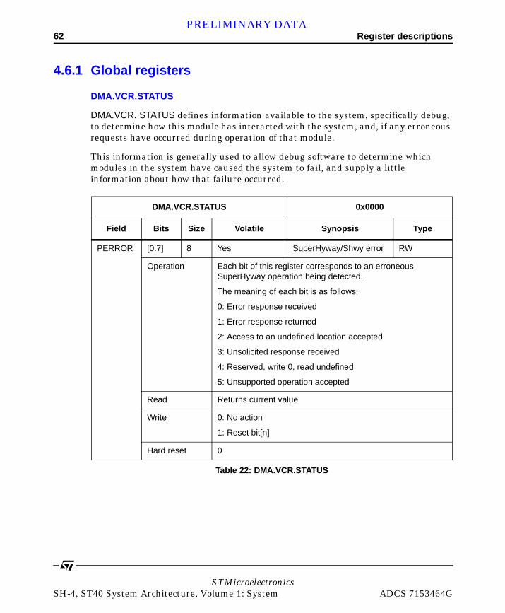
62 Register descriptionsPRELIMINARY DATA
4.6.1 Global registers
DMA.VCR.STATUS
DMA.VCR. STATUS defines information available to the system, specifically debug, to determine how this module has interacted with the system, and, if any erroneous requests have occurred during operation of that module.
This information is generally used to allow debug software to determine which modules in the system have caused the system to fail, and supply a little information about how that failure occurred.
DMA.VCR.STATUS 0x0000
Field Bits Size Volatile Synopsis Type
PERROR [0:7] 8 Yes SuperHyway/Shwy error RW
Operation Each bit of this register corresponds to an erroneous SuperHyway operation being detected.
The meaning of each bit is as follows:
0: Error response received
1: Error response returned
2: Access to an undefined location accepted
3: Unsolicited response received
4: Reserved, write 0, read undefined
5: Unsupported operation accepted
Read Returns current value
Write 0: No action
1: Reset bit[n]
Hard reset 0
Table 22: DMA.VCR.STATUS
STMicroelectronicsSH-4, ST40 System Architecture, Volume 1: System ADCS 7153464G

Register descriptions 63PRELIMINARY DATA
MERROR [8:15] 8 Yes Module error RW
Operation Each bit of this register corresponds to an erroneous module operation being detected.
0: Alignment error
An alignment error will occur if a channel is mis-programming with an unalignable transfer on a channel which enforces alignment checks.
1 to 7: Reserved
Read Returns current value
Write 0: No action
1: Reset bit[n]
Hard reset 0x00
MOD_ID [16:31] 16 No Module identity RO
Operation Used to indicate the module type
Read Returns module ID
Write Ignored
Hard Reset Reserved
DMA.VCR.STATUS 0x0000
Field Bits Size Volatile Synopsis Type
Table 22: DMA.VCR.STATUS
STMicroelectronicsADCS 7153464G SH-4, ST40 System Architecture, Volume 1: System

64 Register descriptionsPRELIMINARY DATA
DMA.VCR.VERSION
DMA.VCR.VERSION defines the module type and revision number.
DMA.VCR.VERSION 0x0008
Field Bits Size Volatile Synopsis Type
MOD_VER [0:15] 16 No Module version RO
Operation Used to indicate the module type
Read Returns module version
Write Ignored
Hard reset 0
MOD_SIZE
[16:31] 16 No Module size RO
Operation Module size defined in blocks of 64 Kbytes
Read Reads 0x0001
Write Ignored
Hard reset 0x0001
Table 23: DMA.VCR.VERSION
STMicroelectronicsSH-4, ST40 System Architecture, Volume 1: System ADCS 7153464G

Register descriptions 65PRELIMINARY DATA
DMA.ENABLE
DMA.ENABLE defines a global mechanism for software to enable one or more channels rapidly.1
DMA.ENABLE 0x0010
Field Bits Size Volatile Synopsis Type
CHANNEL [0:4] 6 Yes DMA enable RW
Operation Bit[n] is used to enable channel[n]
Read 1: DMA channel[n] enabled
0: DMA channel[n] disabled
Write 1: Enable DMA channel[n]
0: No action
Hard reset 0x00
- [6:31] 26 - Reserved -
Operation Reserved
Read Undefined
Write 0
Hard reset Undefined
Table 24: DMA.ENABLE
1. A channel is enabled only when both the channel and global enables are set
STMicroelectronicsADCS 7153464G SH-4, ST40 System Architecture, Volume 1: System
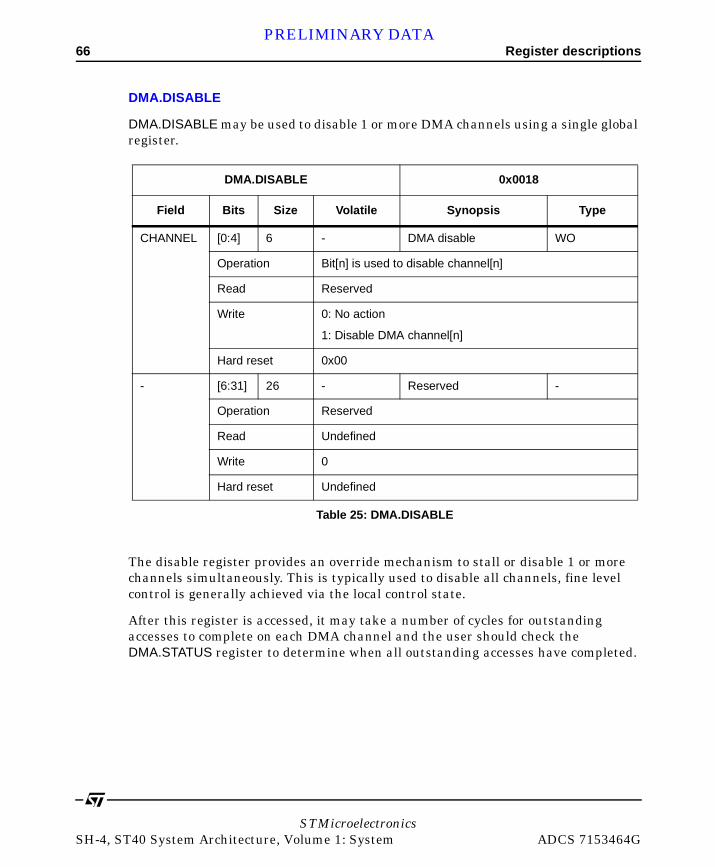
66 Register descriptionsPRELIMINARY DATA
DMA.DISABLE
DMA.DISABLE may be used to disable 1 or more DMA channels using a single global register.
The disable register provides an override mechanism to stall or disable 1 or more channels simultaneously. This is typically used to disable all channels, fine level control is generally achieved via the local control state.
After this register is accessed, it may take a number of cycles for outstanding accesses to complete on each DMA channel and the user should check the DMA.STATUS register to determine when all outstanding accesses have completed.
DMA.DISABLE 0x0018
Field Bits Size Volatile Synopsis Type
CHANNEL [0:4] 6 - DMA disable WO
Operation Bit[n] is used to disable channel[n]
Read Reserved
Write 0: No action
1: Disable DMA channel[n]
Hard reset 0x00
- [6:31] 26 - Reserved -
Operation Reserved
Read Undefined
Write 0
Hard reset Undefined
Table 25: DMA.DISABLE
STMicroelectronicsSH-4, ST40 System Architecture, Volume 1: System ADCS 7153464G
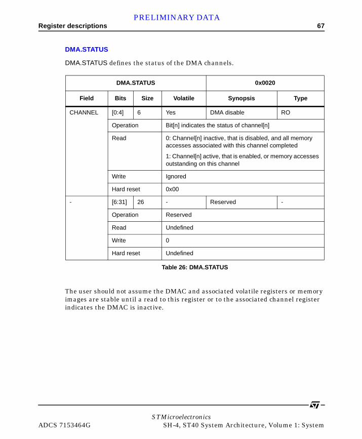
Register descriptions 67PRELIMINARY DATA
DMA.STATUS
DMA.STATUS defines the status of the DMA channels.
The user should not assume the DMAC and associated volatile registers or memory images are stable until a read to this register or to the associated channel register indicates the DMAC is inactive.
DMA.STATUS 0x0020
Field Bits Size Volatile Synopsis Type
CHANNEL [0:4] 6 Yes DMA disable RO
Operation Bit[n] indicates the status of channel[n]
Read 0: Channel[n] inactive, that is disabled, and all memory accesses associated with this channel completed
1: Channel[n] active, that is enabled, or memory accesses outstanding on this channel
Write Ignored
Hard reset 0x00
- [6:31] 26 - Reserved -
Operation Reserved
Read Undefined
Write 0
Hard reset Undefined
Table 26: DMA.STATUS
STMicroelectronicsADCS 7153464G SH-4, ST40 System Architecture, Volume 1: System

68 Register descriptionsPRELIMINARY DATA
DMA.INTERRUPT
DMA.INTERRUPT summarizes the interrupt status of all channels. It may be read to determine which channel caused an interrupt to be asserted.
To clear or determine the cause of the interrupt on a specific channel, the associated channel register DMA.CHAN[N].STATUS and DMA.CHAN[N].CONTROL registers should be accessed.
DMA.INTERRUPT 0x0028
Field Bits Size Volatile Synopsis Type
CHANNEL [0:4] 6 Yes DMA interrupt status RO
Operation If bit[n] is set, an unserviced DMA interrupt occurred on channel[n]
Read 0: No outstanding interrupts on channel[n]
1: Unserviced interrupt on channel[n]
Write Ignored
Hard reset 0x00
- [6:31] 26 - Reserved -
Operation Reserved
Read Undefined
Write 0
Hard reset Undefined
Table 27: DMA.INTERRUPT
STMicroelectronicsSH-4, ST40 System Architecture, Volume 1: System ADCS 7153464G

Register descriptions 69PRELIMINARY DATA
DMA.ERROR
DMA.ERROR summarizes the error status of all channels. It may be read to determine which channel caused an error condition to occur.
To clear or determine the cause of the interrupt on a specific channel, the associated channel register DMA.CHAN[N].STATUS and DMA.CHAN[N].CONTROL registers should be accessed.
DMA.ERROR 0x0030
Field Bits Size Volatile Synopsis Type
ERROR [0:4] 6 Yes DMA error status RO
Operation If bit[n] is set, an unserviced error interrupt occurred on channel[n]
Read Returns current value
Write Ignored
Hard reset 0x00
- [6:31] 26 - Reserved -
Operation Reserved
Read Undefined
Write 0
Hard reset Undefined
Table 28: DMA.ERROR
STMicroelectronicsADCS 7153464G SH-4, ST40 System Architecture, Volume 1: System

70 Register descriptionsPRELIMINARY DATA
DMA.DEFINED
DMA.DEFINED is a five channel implementation of the DMAC, future variants which implement different numbers or types of channel.
DMA.HANDSHAKE
DMA.HANDSHAKE defines the protocol for a request from a peripheral.
DMA.DEFINED 0x0038
Field Bits Size Volatile Synopsis Type
DEFINED [0:31] 32 No DMA channel defined RO
Operation If bit[n] set, channel[n] is implemented
Read 0x0000001F
Write Ignored
Hard reset 0x0000001F
Table 29: DMA.DEFINED
DMA.HANDSHAKE 0x0040
Field Bits Size Volatile Synopsis Type
CHANNEL [0:31] 32 No DMA request handshake
RW
Operation If bit[n] is set, DMA request channel[n] implements DREQ/ DRACK protocol.
If bit[n] is not set, it implements DREQ only.
Read Returns current value
Write Updates current value
Hard reset 0x00
Table 30: DMA.HANDSHAKE
STMicroelectronicsSH-4, ST40 System Architecture, Volume 1: System ADCS 7153464G

Register descriptions 71PRELIMINARY DATA
4.6.2 Channel-specific registers
DMA.CHAN[n].IDENTITY
DMA.CHAN[N].IDENTITY describes the type and facilities of a DMA channel.
DMA.CHAN[n].IDENTITY (n = 0 to 4)
((n + 1) * 0x100) + 0x00
Field Bits Size Volatile Synopsis Type
TYPE [0:3] 4 No Channel DMA type RO
Operation Identifies DMA channel type. Valid values are:
0000: No channel
0001: Reserved
0010: Single linked list, list of basic DMAs
0011: Reserved
0100: Table of multiplexed single DMAs
0100 to 1111: Reserved
Read Channel 0: 0x4
Channel[1:4] = 0x2
Write Ignored
Hard reset Channel 0: 0x4
Channel[1:4] = 0x2
Table 31: DMA.CHAN[n].IDENTITY
STMicroelectronicsADCS 7153464G SH-4, ST40 System Architecture, Volume 1: System

72 Register descriptionsPRELIMINARY DATA
TIMING [4:7] 4 No Channel timing model RO
Operation Identifies supported timings models on this channel. Valid values are:
0000: Free running only
0001= Triggered (on hardware event, complete DMA)
0010: Paced (on hardware event, transfer single data unit and wait for next event)
0011: Both triggering and pacing supported on this channel
0100 to1111 Reserved
Read Channel[0:4] = 0x3
Write Ignored
Hard reset Channel[0:4] = 0x3
DMA.CHAN[n].IDENTITY (n = 0 to 4)
((n + 1) * 0x100) + 0x00
Field Bits Size Volatile Synopsis Type
Table 31: DMA.CHAN[n].IDENTITY
STMicroelectronicsSH-4, ST40 System Architecture, Volume 1: System ADCS 7153464G

Register descriptions 73PRELIMINARY DATA
UNIT [8:15] 8 No DMA data units RO
Operation Identifies the data units supported by the channel, valid values are:
Bit 8 set: Support for single byte units
Bit 9 set: Support for 2 byte units
Bit 10 set: Support for 4 byte units
Bit 11 set: Support for 8 byte units
Bit 12 set: Support for 16 byte units
Bit 13 set: Support for 32 byte units
Bit 14 to 15: Reserved
Read Channel[0:4]: 0x3F
Write Ignored
Hard reset Channel[0:4]: 0x3F
DATA [16:23] 8 No Channel data structures RO
Operation Defines the data structures supported by this channel.
Bit 16 set: Support for fixed address (0D)
Bit 17 set: Support for 1D incrementing
Bit 18 set: Support for 1D decrementing
Bit 19 set: Support for 2D incrementing
Bit 20 set: Support for 2D decrementing
Bit 21 to 23: Reserved
Read Channel[0:4]: 0x1F
Write Ignored
Hard reset Channel[0:4]: 0x1F
DMA.CHAN[n].IDENTITY (n = 0 to 4)
((n + 1) * 0x100) + 0x00
Field Bits Size Volatile Synopsis Type
Table 31: DMA.CHAN[n].IDENTITY
STMicroelectronicsADCS 7153464G SH-4, ST40 System Architecture, Volume 1: System
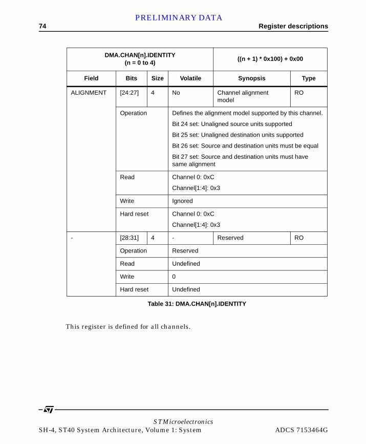
74 Register descriptionsPRELIMINARY DATA
This register is defined for all channels.
ALIGNMENT [24:27] 4 No Channel alignment model
RO
Operation Defines the alignment model supported by this channel.
Bit 24 set: Unaligned source units supported
Bit 25 set: Unaligned destination units supported
Bit 26 set: Source and destination units must be equal
Bit 27 set: Source and destination units must have same alignment
Read Channel 0: 0xC
Channel[1:4]: 0x3
Write Ignored
Hard reset Channel 0: 0xC
Channel[1:4]: 0x3
- [28:31] 4 - Reserved RO
Operation Reserved
Read Undefined
Write 0
Hard reset Undefined
DMA.CHAN[n].IDENTITY (n = 0 to 4)
((n + 1) * 0x100) + 0x00
Field Bits Size Volatile Synopsis Type
Table 31: DMA.CHAN[n].IDENTITY
STMicroelectronicsSH-4, ST40 System Architecture, Volume 1: System ADCS 7153464G

Register descriptions 75PRELIMINARY DATA
DMA.CHAN[n].ENABLE
DMA.CHAN[n].ENABLE controls the behavior of a channel.
DMA.CHAN[n].ENABLE (n = 0 to 4)
((n + 1) * 0x100) + 0x08
Field Bits Size Volatile Synopsis Type
CHANNEL [0] 1 Yes Enable DMA channel RW
Operation Enables this DMA channel
Read If set, channel is enabled
Write 0: No action
1: Enable
Hard reset 0
COMPLETE [1] 1 Yes Enable DMA complete RW
Operation Enables the channel complete interrupt
Read If set, DMA complete interrupt enabled
Write 0: No action
1: Enable
Hard reset 0
BUS_ERROR [2] 1 Yes Enable bus errors RW
Operation Enables DMA bus error interrupts
Read If set, DMA error interrupt enabled
Write 0: No action
1: Enable
Hard reset 0
Table 32: DMA.CHAN[n].ENABLE
STMicroelectronicsADCS 7153464G SH-4, ST40 System Architecture, Volume 1: System
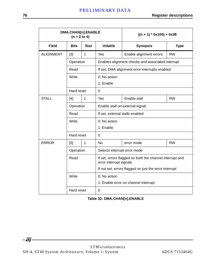
76 Register descriptionsPRELIMINARY DATA
ALIGNMENT [3] 1 Yes Enable alignment errors RW
Operation Enables alignment checks and associated interrupt
Read If set, DMA alignment error interrupts enabled
Write 0: No action
1: Enable
Hard reset 0
STALL [4] 1 Yes Enable stall RW
Operation Enable stall on external signal
Read If set, external stalls enabled
Write 0: No action
1: Enable
Hard reset 0
ERROR [5] 1 No error mode RW
Operation Selects interrupt error mode
Read If set, errors flagged on both the channel interrupt and error interrupt signals
If not set, errors flagged on just the error interrupt
Write 0: No action
1: Enable error on channel interrupt
Hard reset 0
DMA.CHAN[n].ENABLE (n = 0 to 4)
((n + 1) * 0x100) + 0x08
Field Bits Size Volatile Synopsis Type
Table 32: DMA.CHAN[n].ENABLE
STMicroelectronicsSH-4, ST40 System Architecture, Volume 1: System ADCS 7153464G
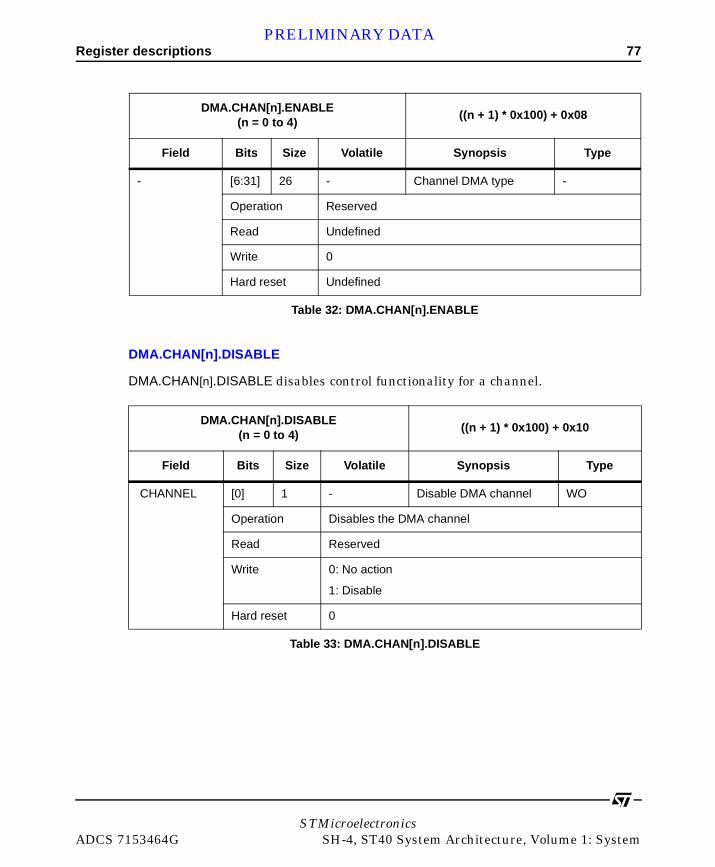
Register descriptions 77PRELIMINARY DATA
DMA.CHAN[n].DISABLE
DMA.CHAN[n].DISABLE disables control functionality for a channel.
- [6:31] 26 - Channel DMA type -
Operation Reserved
Read Undefined
Write 0
Hard reset Undefined
DMA.CHAN[n].ENABLE (n = 0 to 4)
((n + 1) * 0x100) + 0x08
Field Bits Size Volatile Synopsis Type
Table 32: DMA.CHAN[n].ENABLE
DMA.CHAN[n].DISABLE (n = 0 to 4)
((n + 1) * 0x100) + 0x10
Field Bits Size Volatile Synopsis Type
CHANNEL [0] 1 - Disable DMA channel WO
Operation Disables the DMA channel
Read Reserved
Write 0: No action
1: Disable
Hard reset 0
Table 33: DMA.CHAN[n].DISABLE
STMicroelectronicsADCS 7153464G SH-4, ST40 System Architecture, Volume 1: System

78 Register descriptionsPRELIMINARY DATA
COMPLETE [1] 1 - Disable DMA complete WO
Operation Disables interrupts on DMA complete
Read Reserved
Write 0: No action
1: Disable
Hard reset 0
BUS_ERROR [2] 1 - Disable bus errors WO
Operation Disables interrupts on channel’s bus errors
Read Reserved
Write 0: No action
1: Disable
Hard reset 0
ALIGNMENT [3] 1 - Disable alignment errors WO
Operation Disables interrupt on misaligned accesses on the channel
Read Reserved
Write 0: No action
1: Disable
Hard reset 0
DMA.CHAN[n].DISABLE (n = 0 to 4)
((n + 1) * 0x100) + 0x10
Field Bits Size Volatile Synopsis Type
Table 33: DMA.CHAN[n].DISABLE
STMicroelectronicsSH-4, ST40 System Architecture, Volume 1: System ADCS 7153464G
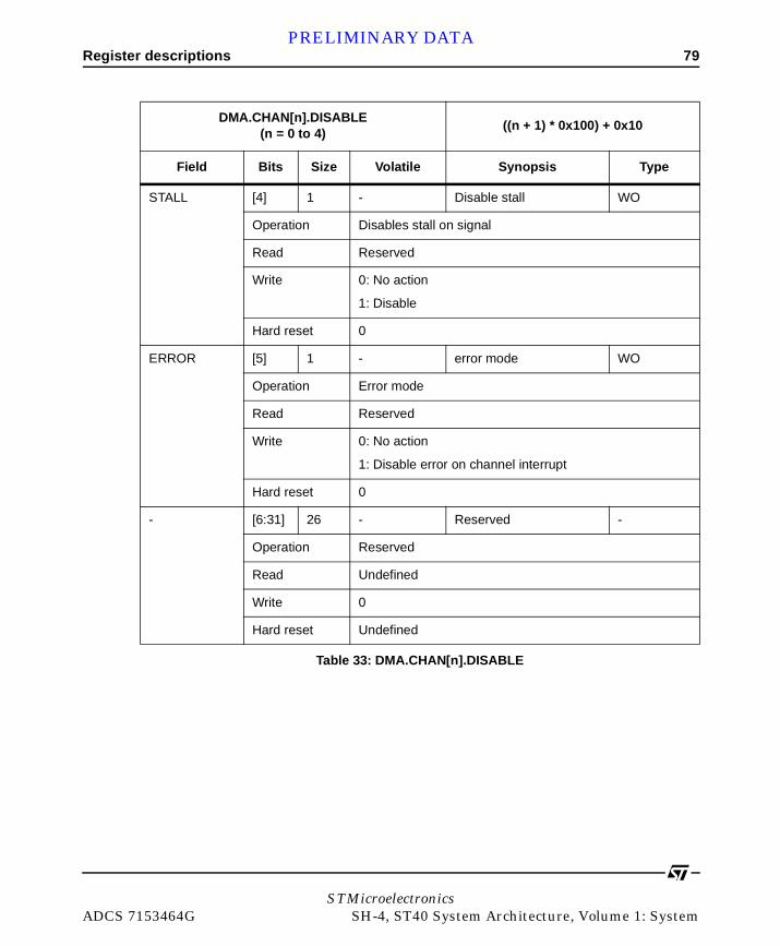
Register descriptions 79PRELIMINARY DATA
STALL [4] 1 - Disable stall WO
Operation Disables stall on signal
Read Reserved
Write 0: No action
1: Disable
Hard reset 0
ERROR [5] 1 - error mode WO
Operation Error mode
Read Reserved
Write 0: No action
1: Disable error on channel interrupt
Hard reset 0
- [6:31] 26 - Reserved -
Operation Reserved
Read Undefined
Write 0
Hard reset Undefined
DMA.CHAN[n].DISABLE (n = 0 to 4)
((n + 1) * 0x100) + 0x10
Field Bits Size Volatile Synopsis Type
Table 33: DMA.CHAN[n].DISABLE
STMicroelectronicsADCS 7153464G SH-4, ST40 System Architecture, Volume 1: System
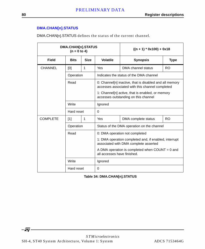
80 Register descriptionsPRELIMINARY DATA
DMA.CHAN[n].STATUS
DMA.CHAN[n].STATUS defines the status of the current channel.
DMA.CHAN[n].STATUS (n = 0 to 4)
((n + 1) * 0x100) + 0x18
Field Bits Size Volatile Synopsis Type
CHANNEL [0] 1 Yes DMA channel status RO
Operation Indicates the status of the DMA channel
Read 0: Channel[n] inactive, that is disabled and all memory accesses associated with this channel completed
1: Channel[n] active, that is enabled, or memory accesses outstanding on this channel
Write Ignored
Hard reset 0
COMPLETE [1] 1 Yes DMA complete status RO
Operation Status of the DMA operation on the channel
Read 0: DMA operation not completed
1: DMA operation completed and, if enabled, interrupt associated with DMA complete asserted
A DMA operation is completed when COUNT = 0 and all accesses have finished.
Write Ignored
Hard reset 0
Table 34: DMA.CHAN[n].STATUS
STMicroelectronicsSH-4, ST40 System Architecture, Volume 1: System ADCS 7153464G

Register descriptions 81PRELIMINARY DATA
BUS_ERROR [2] 1 Yes Bus error status RO
Operation Indicates the status of the bus errors on this channel
Read 0: No outstanding bus errors on the channel
1: Memory access from the channel returned an outstanding bus error to this device and, if enabled, interrupt associated with errors on channel is asserted
Write Ignored
Hard reset 0
ALIGNMENT [3] 1 Yes Alignment status RO
Operation Status of alignment errors on the channel
Read 0: No unaligned accesses occurred
1: Unit transfer size and address cannot be aligned and, if enabled, interrupt associated with errors on the channel is asserted
Write Ignored
Hard reset 0
STALL [4] 1 Yes Stall status RO
Operation Status of stall on the channel
Read 0: Channel not stalled
1: Channel stalled by external stall request
Write Ignored
Hard reset 0
DMA.CHAN[n].STATUS (n = 0 to 4)
((n + 1) * 0x100) + 0x18
Field Bits Size Volatile Synopsis Type
Table 34: DMA.CHAN[n].STATUS
STMicroelectronicsADCS 7153464G SH-4, ST40 System Architecture, Volume 1: System

82 Register descriptionsPRELIMINARY DATA
UPDATE [6] 1 Yes Update status WO
Operation Status of link list update request
Read 0: No request outstanding
1: Linked list update request outstanding
Write Ignored
Hard reset 0
- [5]
[7:31]
26 - - -
Operation Reserved
Read Undefined
Write 0
Hard reset Undefined
DMA.CHAN[n].STATUS (n = 0 to 4)
((n + 1) * 0x100) + 0x18
Field Bits Size Volatile Synopsis Type
Table 34: DMA.CHAN[n].STATUS
STMicroelectronicsSH-4, ST40 System Architecture, Volume 1: System ADCS 7153464G

Register descriptions 83PRELIMINARY DATA
DMA.CHAN[n].ACTION
DMA.CHAN[n].ACTION causes an action associated with a channel.
DMA.CHAN[n].ACTION (n = 0 to 4)
((n + 1) * 0x100) + 0x20
Field Bits Size Volatile Synopsis Type
CHANNEL [0] 1 - - -
Operation Reserved
Read Undefined
Write 0
Hard reset Undefined
COMPLETE [1] 1 - DMA complete status WO
Operation Change status of DMA complete on channel
Read Undefined
Write 0: No action
1: Reset DMA complete status bit and associated interrupt
Hard reset 0
BUS_ERROR [2] 1 - Bus error status WO
Operation Change status of bus error on channel
Read Undefined
Write 0: No action
1: Reset DMA bus error status bit and associated interrupt
Hard reset 0
Table 35: DMA.CHAN[n].ACTION
STMicroelectronicsADCS 7153464G SH-4, ST40 System Architecture, Volume 1: System
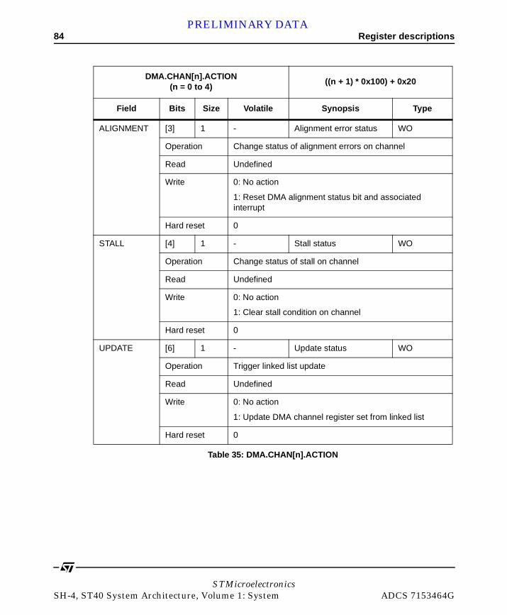
84 Register descriptionsPRELIMINARY DATA
ALIGNMENT [3] 1 - Alignment error status WO
Operation Change status of alignment errors on channel
Read Undefined
Write 0: No action
1: Reset DMA alignment status bit and associated interrupt
Hard reset 0
STALL [4] 1 - Stall status WO
Operation Change status of stall on channel
Read Undefined
Write 0: No action
1: Clear stall condition on channel
Hard reset 0
UPDATE [6] 1 - Update status WO
Operation Trigger linked list update
Read Undefined
Write 0: No action
1: Update DMA channel register set from linked list
Hard reset 0
DMA.CHAN[n].ACTION (n = 0 to 4)
((n + 1) * 0x100) + 0x20
Field Bits Size Volatile Synopsis Type
Table 35: DMA.CHAN[n].ACTION
STMicroelectronicsSH-4, ST40 System Architecture, Volume 1: System ADCS 7153464G

Register descriptions 85PRELIMINARY DATA
DMA.CHAN[n].POINTER
DMA.CHAN[n].POINTER contains the value of the pointer used to fetch the current control information.
- [5], [7:31]
26 - -
Operation Reserved
Read Undefined
Write 0
Hard reset Undefined
DMA.CHAN[n].ACTION (n = 0 to 4)
((n + 1) * 0x100) + 0x20
Field Bits Size Volatile Synopsis Type
Table 35: DMA.CHAN[n].ACTION
DMA.CHAN[n].POINTER (n = 0 to 4)
((n + 1) * 0x100) + 0x28
Field Bits Size Volatile Synopsis Type
ADDRESS [3:31] 29 Yes Current channel pointer RO
Operation Indicates location of last register update
Read Returns current value
Write Ignored
Hard reset 0
Table 36: DMA.CHAN[n].POINTER
STMicroelectronicsADCS 7153464G SH-4, ST40 System Architecture, Volume 1: System
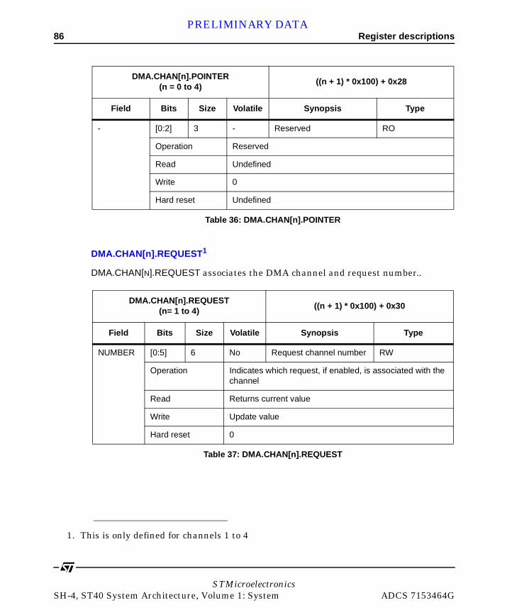
86 Register descriptionsPRELIMINARY DATA
DMA.CHAN[n].REQUEST1
DMA.CHAN[N].REQUEST associates the DMA channel and request number..
- [0:2] 3 - Reserved RO
Operation Reserved
Read Undefined
Write 0
Hard reset Undefined
DMA.CHAN[n].POINTER (n = 0 to 4)
((n + 1) * 0x100) + 0x28
Field Bits Size Volatile Synopsis Type
Table 36: DMA.CHAN[n].POINTER
1. This is only defined for channels 1 to 4
DMA.CHAN[n].REQUEST (n= 1 to 4)
((n + 1) * 0x100) + 0x30
Field Bits Size Volatile Synopsis Type
NUMBER [0:5] 6 No Request channel number RW
Operation Indicates which request, if enabled, is associated with the channel
Read Returns current value
Write Update value
Hard reset 0
Table 37: DMA.CHAN[n].REQUEST
STMicroelectronicsSH-4, ST40 System Architecture, Volume 1: System ADCS 7153464G

Register descriptions 87PRELIMINARY DATA
OFFSET [8:15] 8 No subchannel interrupt RW
Operation Minimum offset between acknowledgment of request, and subsequent sampling of same request
Read Returns current state
Write Updates current state
Hard reset 0
- [6:7]
[16:31]
2
16
- Reserved RO
Operation Reserved
Read Undefined
Write 0
Hard reset Undefined
DMA.CHAN[n].REQUEST (n= 1 to 4)
((n + 1) * 0x100) + 0x30
Field Bits Size Volatile Synopsis Type
Table 37: DMA.CHAN[n].REQUEST
STMicroelectronicsADCS 7153464G SH-4, ST40 System Architecture, Volume 1: System

88 Register descriptionsPRELIMINARY DATA
DMA.CHAN[n].SUBBASE1
For channel 0, DMA.CHAN[N].SUBBASE points to the base address of the channel table stored in memory.
1. Only defined for channel 0
DMA.CHAN[n].SUBBASE(n = 0)
((n + 1) * 0x100) + 0x30
Field Bits Size Volatile Synopsis Type
ADDRESS [8:31] 24 No Table base address RW
Operation Pointer to base address of subchannel table
Read Returns current value
Write Updates current value
Hard reset 0
- [0:7] 8 - Reserved
Operation Reserved
Read Undefined
Write 0
Hard reset Undefined
Table 38: DMA.CHAN[n].SUBBASE
STMicroelectronicsSH-4, ST40 System Architecture, Volume 1: System ADCS 7153464G

Register descriptions 89PRELIMINARY DATA
DMA.CHAN[n].SUBENABLE1
For channel 0 DMA.CHAN[N].SUBENABLE defines which subchannel is enabled.
If subchannel[i] is enabled and request[i] is asserted then the following actions occur:
1 The information is stored in memory for subchannel[i] to be loaded in the register state.
2 1 or more transfer units are completed on subchannel[i].
3 The information is stored in memory for subchannel[i] to be updated with new register state.
If channel 0 is enabled and subchannel[i] is not enabled then events on request[i] will be ignored.
1. Only defined for channel 0
DMA.CHAN[n].SUBENABLE(n = 0)
((n + 1) * 0x100) + 0x38
Field Bits Size Volatile Synopsis Type
SUBCHANNEL [0:31] 32 Yes Enable subchannel RW
Operation Enables DMA subchannel
Read If set, current subchannel enabled
Write 0: No action
1: Enables subchannel[i]
Hard reset 0
Table 39: DMA.CHAN[n].SUBENABLE
STMicroelectronicsADCS 7153464G SH-4, ST40 System Architecture, Volume 1: System
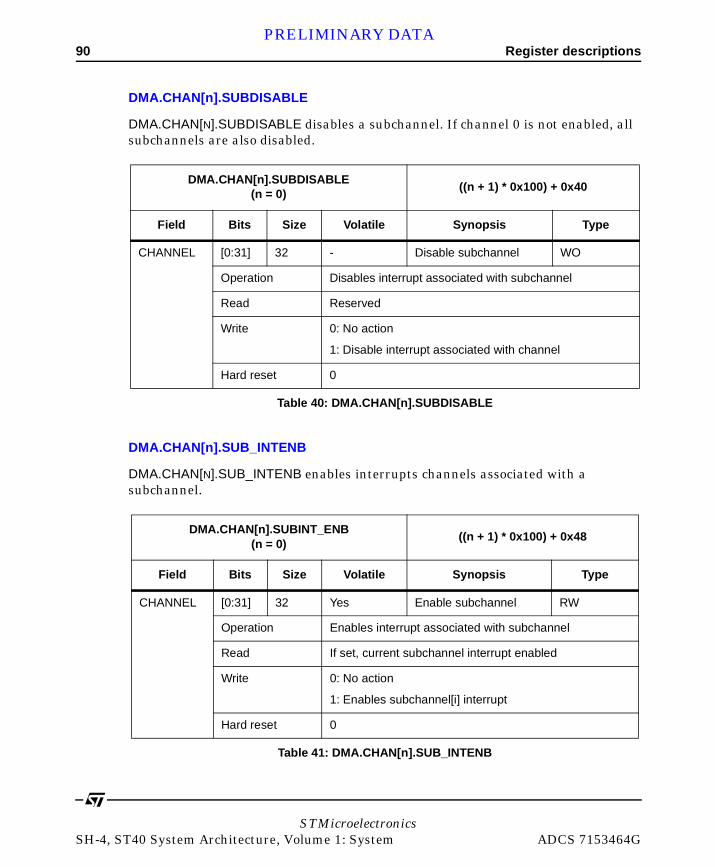
90 Register descriptionsPRELIMINARY DATA
DMA.CHAN[n].SUBDISABLE
DMA.CHAN[N].SUBDISABLE disables a subchannel. If channel 0 is not enabled, all subchannels are also disabled.
DMA.CHAN[n].SUB_INTENB
DMA.CHAN[N].SUB_INTENB enables interrupts channels associated with a subchannel.
DMA.CHAN[n].SUBDISABLE(n = 0)
((n + 1) * 0x100) + 0x40
Field Bits Size Volatile Synopsis Type
CHANNEL [0:31] 32 - Disable subchannel WO
Operation Disables interrupt associated with subchannel
Read Reserved
Write 0: No action
1: Disable interrupt associated with channel
Hard reset 0
Table 40: DMA.CHAN[n].SUBDISABLE
DMA.CHAN[n].SUBINT_ENB(n = 0)
((n + 1) * 0x100) + 0x48
Field Bits Size Volatile Synopsis Type
CHANNEL [0:31] 32 Yes Enable subchannel RW
Operation Enables interrupt associated with subchannel
Read If set, current subchannel interrupt enabled
Write 0: No action
1: Enables subchannel[i] interrupt
Hard reset 0
Table 41: DMA.CHAN[n].SUB_INTENB
STMicroelectronicsSH-4, ST40 System Architecture, Volume 1: System ADCS 7153464G
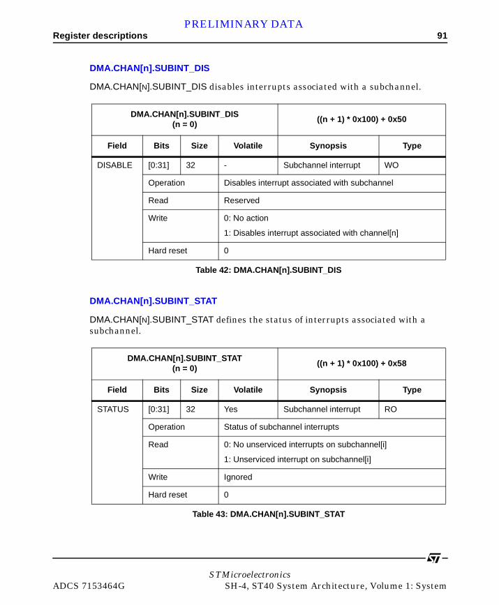
Register descriptions 91PRELIMINARY DATA
DMA.CHAN[n].SUBINT_DIS
DMA.CHAN[N].SUBINT_DIS disables interrupts associated with a subchannel.
DMA.CHAN[n].SUBINT_STAT
DMA.CHAN[N].SUBINT_STAT defines the status of interrupts associated with a subchannel.
DMA.CHAN[n].SUBINT_DIS(n = 0)
((n + 1) * 0x100) + 0x50
Field Bits Size Volatile Synopsis Type
DISABLE [0:31] 32 - Subchannel interrupt WO
Operation Disables interrupt associated with subchannel
Read Reserved
Write 0: No action
1: Disables interrupt associated with channel[n]
Hard reset 0
Table 42: DMA.CHAN[n].SUBINT_DIS
DMA.CHAN[n].SUBINT_STAT(n = 0)
((n + 1) * 0x100) + 0x58
Field Bits Size Volatile Synopsis Type
STATUS [0:31] 32 Yes Subchannel interrupt RO
Operation Status of subchannel interrupts
Read 0: No unserviced interrupts on subchannel[i]
1: Unserviced interrupt on subchannel[i]
Write Ignored
Hard reset 0
Table 43: DMA.CHAN[n].SUBINT_STAT
STMicroelectronicsADCS 7153464G SH-4, ST40 System Architecture, Volume 1: System

92 Register descriptionsPRELIMINARY DATA
DMA.CHAN[n].SUBINT_ACT
DMA.CHAN[N].SUBINT_ACT clears interrupt status associated with a subchannel.
DMA.CHAN[n].SUBINT_ACT(n = 0)
((n + 1) * 0x100) + 0x60
Field Bits Size Volatile Synopsis Type
CONTROL [0:31] 32 - Subchannel interrupt WO
Operation Clear interrupt associated with subchannel
Read Reserved
Write 0: No action
1: Clear interrupt status associated with bit[i]
Hard reset 0
Table 44: DMA.CHAN[n].SUBINT_ACT
STMicroelectronicsSH-4, ST40 System Architecture, Volume 1: System ADCS 7153464G
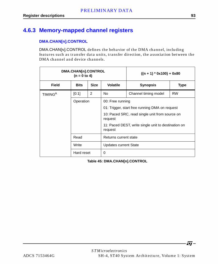
Register descriptions 93PRELIMINARY DATA
4.6.3 Memory-mapped channel registers
DMA.CHAN[n].CONTROL
DMA.CHAN[N].CONTROL defines the behavior of the DMA channel, including features such as transfer data units, transfer direction, the association between the DMA channel and device channels.
DMA.CHAN[n].CONTROL(n = 0 to 4)
((n + 1) * 0x100) + 0x80
Field Bits Size Volatile Synopsis Type
TIMINGA [0:1] 2 No Channel timing model RW
Operation 00: Free running
01: Trigger, start free running DMA on request
10: Paced SRC, read single unit from source on request
11: Paced DEST, write single unit to destination on request
Read Returns current state
Write Updates current State
Hard reset 0
Table 45: DMA.CHAN[n].CONTROL
STMicroelectronicsADCS 7153464G SH-4, ST40 System Architecture, Volume 1: System

94 Register descriptionsPRELIMINARY DATA
LIST_ENB [7] 1 No link list enable RW
Operation Defines whether the DMA is part of a linked list, and if so the behavior on normal DMA completion (channels 1 to 4 only)
0: Not part of, or is the final element of, the linked list
The DMAC asserts the channel complete interrupt if the associated interrupt is enabled.
1: An element within a list
The DMAC does not assert the channel complete and updates the memory mapped register from the linked list.
Read Returns current state
Write Updates current state
Hard reset Undefined
SUB_OFFSETB [8:15] 8 No Subchannel offset RW
Operation Minimum offset between acknowledgment of a request, and subsequent sampling of the same event
Read Returns current state
Write Updates current state
Hard reset 0
DMA.CHAN[n].CONTROL(n = 0 to 4)
((n + 1) * 0x100) + 0x80
Field Bits Size Volatile Synopsis Type
Table 45: DMA.CHAN[n].CONTROL
STMicroelectronicsSH-4, ST40 System Architecture, Volume 1: System ADCS 7153464G

Register descriptions 95PRELIMINARY DATA
SRC_TYPE [16:18] 3 No Source data type RW
Operation Defines the source data structure:
000: Constant source
001: Linear incrementing source
010: Linear decrementing source
011: 2D incrementing source
100: 2D decrementing source
101 to 111: Reserved
Read Returns current state
Write Updates current state
Hard reset 0
SRC_UNITC [19:21] 3 No Source transfer unit RW
Operation Defines the source transfer unit:
000: Byte
001: 2 bytes
010: 4 bytes
011: 8 bytes
100: 16 bytes
101: 32 bytes
110 to 111: Reserved
Read Returns current state
Write Updates current state
Hard reset 0
DMA.CHAN[n].CONTROL(n = 0 to 4)
((n + 1) * 0x100) + 0x80
Field Bits Size Volatile Synopsis Type
Table 45: DMA.CHAN[n].CONTROL
STMicroelectronicsADCS 7153464G SH-4, ST40 System Architecture, Volume 1: System

96 Register descriptionsPRELIMINARY DATA
SRC_UPDATE [22] 1 No Disable source update RW
Operation Defines whether the addressing information associated with a source data structure is updated when reading from a linked list
0: Source update enabled
1: Source update disabled
The information which may be updated includes SAR, SRC_STRIDE, SRC_LENGTH and the 2D transfer offset.
Read Returns current state
Write Updates current state
Hard reset Undefined
DST_TYPE [24:26] 3 No Destination data type RW
Operation Defines the destination data structure
000: Constant source
001: Linear incrementing source
010: Linear decrementing source
011: 2D incrementing source
100: 2D decrementing source
101 to 111: Reserved
Read Returns current state
Write Updates current state
Hard reset 0
DMA.CHAN[n].CONTROL(n = 0 to 4)
((n + 1) * 0x100) + 0x80
Field Bits Size Volatile Synopsis Type
Table 45: DMA.CHAN[n].CONTROL
STMicroelectronicsSH-4, ST40 System Architecture, Volume 1: System ADCS 7153464G

Register descriptions 97PRELIMINARY DATA
DST_UNITC [27:29] 3 No Destination transfer unit RW
Operation Defines the destination transfer unit
000: byte
001: 2 bytes
010: 4 bytes
011: 8 bytes
100: 16 bytes
101: 32 bytes
110 to 111: Reserved
Read Returns current state
Write Updates current state
Hard reset 0
DST_UPDATE [30] 1 No Disable destination update
RW
Operation Defines whether the addressing information associated with a destination data structure is updated when reading from a linked list
0: Destination update enabled
The information which may be updated includes DAR, DST_STRIDE, DST_LENGTH and the 2D transfer offset.
1: Destination update disabled
Read Returns current state
Write Updates current state
Hard reset Undefined
DMA.CHAN[n].CONTROL(n = 0 to 4)
((n + 1) * 0x100) + 0x80
Field Bits Size Volatile Synopsis Type
Table 45: DMA.CHAN[n].CONTROL
STMicroelectronicsADCS 7153464G SH-4, ST40 System Architecture, Volume 1: System

98 Register descriptionsPRELIMINARY DATA
- [2:6]
[23]
[31]
5
1
1
- Reserved
Operation Reserved
Read Undefined
Write 0
Hard reset Undefined
A. Channel 0: source and destination pacing are equivalent
B. Channel 0: defined, channel 1 to 4 reserved
C. Channel 0: source and destination units are the same, DST_UNIT must be equal to SRC_UNIT
DMA.CHAN[n].CONTROL(n = 0 to 4)
((n + 1) * 0x100) + 0x80
Field Bits Size Volatile Synopsis Type
Table 45: DMA.CHAN[n].CONTROL
STMicroelectronicsSH-4, ST40 System Architecture, Volume 1: System ADCS 7153464G

Register descriptions 99PRELIMINARY DATA
DMA.CHAN[n].COUNT
DMA.CHAN[N].COUNT defines the number of bytes to be transferred before this DMA channel completes.
If alignment checks are available and enabled, then this must be an integer multiple of larger of the 2 data units as defined in the DMA.CHAN[N].CONTROL register. If an alignment error occurs, this channel is disabled and no further transfers occur.
DMA.CHAN[n].COUNT(n = 0 to 4)
((n + 1) * 0x100) + 0x88
Field Bits Size Volatile Synopsis Type
BYTES [0:31] 32 Yes Transfer count RW
Operation Number of bytes remaining to be transferred on this channel
Read Returns current value
Write Updates current value
Hard reset 0
Table 46: DMA.CHAN[n].COUNT
STMicroelectronicsADCS 7153464G SH-4, ST40 System Architecture, Volume 1: System

100 Register descriptionsPRELIMINARY DATA
DMA.CHAN[n].SAR
DMA.CHAN[N].SAR defines the starting address of the data source.
If alignment checks are available and enabled, then this must be an integer multiple of larger of the source data unit as defined in the DMA.CHAN[N].CONTROL register. If an alignment error occurs, this channel will be disabled and no further transfers will occur.
If alignment checks are disabled, then the DMA channel will use the largest alignable data unit equal to or smaller than that defined in the DMA.CHAN[N].CONTROL register
DMA.CHAN[n].SAR(n = 0 to 4)
((n + 1) * 0x100) + 0x90
Field Bits Size Volatile Synopsis Type
ADDRESS [0:31] 32 Yes Source address RW
Operation Indicates the address from which the next transfer unit is fetched
This address is incremented or decremented as DMA channel[n] proceeds in accordance with the setting of DMA.CHAN[N].CONTROL.
A write to this register causes internal address state associated with the source data transfer within the DMA to be reset.
Read Returns current value
Write Updates current value
Hard reset 0
Table 47: DMA.CHAN[n].SAR
STMicroelectronicsSH-4, ST40 System Architecture, Volume 1: System ADCS 7153464G
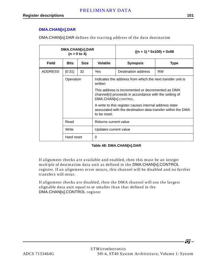
Register descriptions 101PRELIMINARY DATA
DMA.CHAN[n].DAR
DMA.CHAN[N].DAR defines the starting address of the data destination
If alignment checks are available and enabled, then this must be an integer multiple of destination data unit as defined in the DMA.CHAN[N].CONTROL register. If an alignment error occurs, this channel will be disabled and no further transfers will occur.
If alignment checks are disabled, then the DMA channel will use the largest alignable data unit equal to or smaller than that defined in the DMA.CHAN[N].CONTROL register
DMA.CHAN[n].DAR(n = 0 to 4)
((n + 1) * 0x100) + 0x98
Field Bits Size Volatile Synopsis Type
ADDRESS [0:31] 32 Yes Destination address RW
Operation Indicates the address from which the next transfer unit is written
This address is incremented or decremented as DMA channel[n] proceeds in accordance with the setting of DMA.CHAN[N].CONTROL.
A write to this register causes internal address state associated with the destination data transfer within the DMA to be reset.
Read Returns current value
Write Updates current value
Hard reset 0
Table 48: DMA.CHAN[n].DAR
STMicroelectronicsADCS 7153464G SH-4, ST40 System Architecture, Volume 1: System
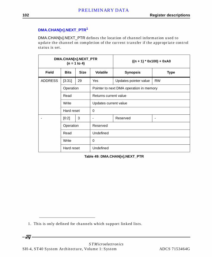
102 Register descriptionsPRELIMINARY DATA
DMA.CHAN[n].NEXT_PTR1
DMA.CHAN[N].NEXT_PTR defines the location of channel information used to update the channel on completion of the current transfer if the appropriate control status is set.
1. This is only defined for channels which support linked lists.
DMA.CHAN[n].NEXT_PTR(n = 1 to 4)
((n + 1) * 0x100) + 0xA0
Field Bits Size Volatile Synopsis Type
ADDRESS [3:31] 29 Yes Updates pointer value RW
Operation Pointer to next DMA operation in memory
Read Returns current value
Write Updates current value
Hard reset 0
- [0:2] 3 - Reserved -
Operation Reserved
Read Undefined
Write 0
Hard reset Undefined
Table 49: DMA.CHAN[n].NEXT_PTR
STMicroelectronicsSH-4, ST40 System Architecture, Volume 1: System ADCS 7153464G

Register descriptions 103PRELIMINARY DATA
DMA.CHAN[n].SRC_LENGTH1
DMA.CHAN[N].SRC_LENGTH defines the length of a line for a 2D data structure.
If alignment checks are available and enabled, then this must be an integer multiple of the source unit as defined in the DMA.CHAN[N].CONTROL register. If an alignment error occurs, this channel will be disabled and no further transfers will occur.
If alignment is not enabled, the DMAC module is responsible for selecting the largest datum size appropriate for the address and length values which is equal to or smaller than that defined in the DMA.CHAN[N].CONTROL register.
1. This is only defined for channels which support 2D transfer structures
DMA.CHAN[n].SRC_LENGTH(n = 1 to 4)
((n + 1) * 0x100) + 0xA8
Field Bits Size Volatile Synopsis Type
COUNT [0:15] 16 Yes Transfer count RW
Operation Length of a line in a source 2D data type
Read Returns current value
Write Updates current value
Hard reset 0
- [16:31] 16 - Reserved -
Operation Reserved
Read Undefined
Write 0
Hard reset Undefined
Table 50: DMA.CHAN[n].SRC_LENGTH
STMicroelectronicsADCS 7153464G SH-4, ST40 System Architecture, Volume 1: System
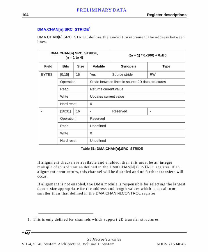
104 Register descriptionsPRELIMINARY DATA
DMA.CHAN[n].SRC_STRIDE1
DMA.CHAN[N].SRC_STRIDE defines the amount to increment the address between lines.
If alignment checks are available and enabled, then this must be an integer multiple of source unit as defined in the DMA.CHAN[N].CONTROL register. If an alignment error occurs, this channel will be disabled and no further transfers will occur.
If alignment is not enabled, the DMA module is responsible for selecting the largest datum size appropriate for the address and length values which is equal to or smaller than that defined in the DMA.CHAN[N].CONTROL register
1. This is only defined for channels which support 2D transfer structures
DMA.CHAN[n].SRC_STRIDE,(n = 1 to 4)
((n + 1) * 0x100) + 0xB0
Field Bits Size Volatile Synopsis Type
BYTES [0:15] 16 Yes Source stride RW
Operation Stride between lines in source 2D data structures
Read Returns current value
Write Updates current value
Hard reset 0
- [16:31] 16 - Reserved -
Operation Reserved
Read Undefined
Write 0
Hard reset Undefined
Table 51: DMA.CHAN[n].SRC_STRIDE
STMicroelectronicsSH-4, ST40 System Architecture, Volume 1: System ADCS 7153464G

Register descriptions 105PRELIMINARY DATA
DMA.CHAN[n].DST_LENGTH1
DMA.CHAN[N].DST_LENGTH defines the length of a line for a 2D data structure.
If alignment checks are available and enabled, then this must be an integer multiple of the destination data unit as defined in the DMA.CHAN[N].CONTROL register. If an alignment error occurs, this channel will be disabled and no further transfers will occur.
If alignment is not enabled, the DMAC module is responsible for selecting the largest datum size appropriate for the address and length values which is equal to or smaller than that defined in the DMA.CHAN[N].CONTROL register.
1. This is only defined for channels which support 2D transfer structures
DMA.CHAN[n].DST_LENGTH (n = 1 to 4)
((n + 1) * 0x100) + 0xB8
Field Bits Size Volatile Synopsis Type
COUNT [0:15] 16 Yes Transfer count RW
Operation Length of a line in a destination 2D data type
Read Returns current value
Write Updates current value
Hard reset 0
- [16:31] 16 - Reserved -
Operation Reserved
Read Undefined
Write 0
Hard reset Undefined
Table 52: DMA.CHAN[n].DST_LENGTH
STMicroelectronicsADCS 7153464G SH-4, ST40 System Architecture, Volume 1: System
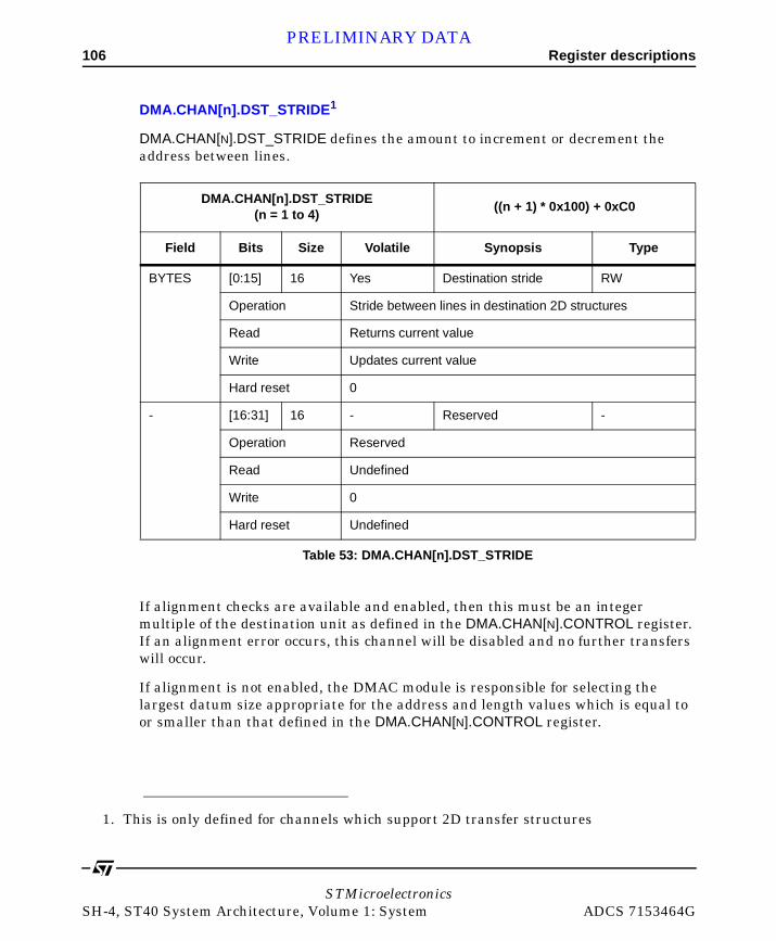
106 Register descriptionsPRELIMINARY DATA
DMA.CHAN[n].DST_STRIDE1
DMA.CHAN[N].DST_STRIDE defines the amount to increment or decrement the address between lines.
If alignment checks are available and enabled, then this must be an integer multiple of the destination unit as defined in the DMA.CHAN[N].CONTROL register. If an alignment error occurs, this channel will be disabled and no further transfers will occur.
If alignment is not enabled, the DMAC module is responsible for selecting the largest datum size appropriate for the address and length values which is equal to or smaller than that defined in the DMA.CHAN[N].CONTROL register.
1. This is only defined for channels which support 2D transfer structures
DMA.CHAN[n].DST_STRIDE (n = 1 to 4)
((n + 1) * 0x100) + 0xC0
Field Bits Size Volatile Synopsis Type
BYTES [0:15] 16 Yes Destination stride RW
Operation Stride between lines in destination 2D structures
Read Returns current value
Write Updates current value
Hard reset 0
- [16:31] 16 - Reserved -
Operation Reserved
Read Undefined
Write 0
Hard reset Undefined
Table 53: DMA.CHAN[n].DST_STRIDE
STMicroelectronicsSH-4, ST40 System Architecture, Volume 1: System ADCS 7153464G

PRELIMINARY DATA
STMicroelectroniADCS 7153464G SH-4, ST40 S
5
Parallel input/output (PIO)The ST40 has 24 bits of parallel input/output (PIO), configured in three 8-bit groups (ports). Each bit is programmable as an output, an input, a bidirectional pin, or as an alternate function output pin. The alternate function connects signals from device peripherals to the pins of the device through the PIO.
Each 8-bit group can also be compared against a register and an interrupt generated when the value is not equal.
Output drivers for the PIO pins, both in PIO mode and the alternate function mode, can be programmed to be push-pull, open drain, or weak pull-up. The weak pull-up configuration avoids the need for pull-up resistors on unused pins while still allowing them to be driven for test purposes.
Each of the 8-bit groups operates as described in the following section.
5.1 PIO ports 0 to 2Each of the 8 bits of a PIO port has a corresponding bit in the PIO registers associated with each port. These registers hold:
• output data for the port (POUT),
• the input data read from the pin (PIN),
• PIO bit configuration registers (PC0, PC1 and PC2),
• the 2 input compare function registers (PCOMP and PMASK).
csystem Architecture, Volume 1: System
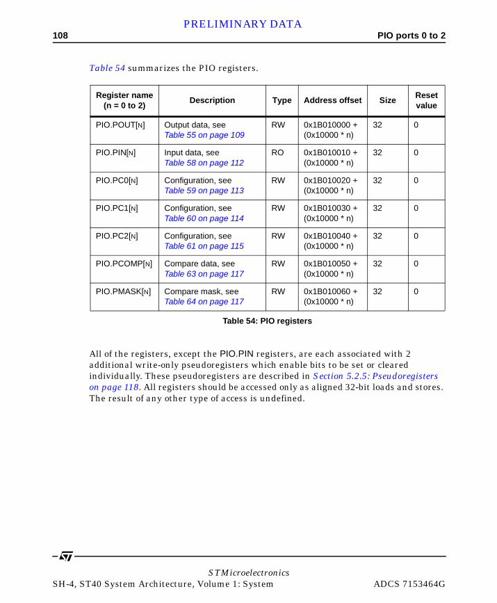
108 PIO ports 0 to 2PRELIMINARY DATA
Table 54 summarizes the PIO registers.
All of the registers, except the PIO.PIN registers, are each associated with 2 additional write-only pseudoregisters which enable bits to be set or cleared individually. These pseudoregisters are described in Section 5.2.5: Pseudoregisters on page 118. All registers should be accessed only as aligned 32-bit loads and stores. The result of any other type of access is undefined.
Register name(n = 0 to 2)
Description Type Address offset SizeReset value
PIO.POUT[N] Output data, seeTable 55 on page 109
RW 0x1B010000 + (0x10000 * n)
32 0
PIO.PIN[N] Input data, seeTable 58 on page 112
RO 0x1B010010 + (0x10000 * n)
32 0
PIO.PC0[N] Configuration, seeTable 59 on page 113
RW 0x1B010020 + (0x10000 * n)
32 0
PIO.PC1[N] Configuration, seeTable 60 on page 114
RW 0x1B010030 + (0x10000 * n)
32 0
PIO.PC2[N] Configuration, seeTable 61 on page 115
RW 0x1B010040 + (0x10000 * n)
32 0
PIO.PCOMP[N] Compare data, seeTable 63 on page 117
RW 0x1B010050 + (0x10000 * n)
32 0
PIO.PMASK[N] Compare mask, seeTable 64 on page 117
RW 0x1B010060 + (0x10000 * n)
32 0
Table 54: PIO registers
STMicroelectronicsSH-4, ST40 System Architecture, Volume 1: System ADCS 7153464G

Register descriptions 109PRELIMINARY DATA
5.2 Register descriptions
5.2.1 Output registers
The 3 PIO.POUT registers are used to specify the data to be output from the port.
PIO.POUT[n](n = 0 to 2)
0x1B010000 + (0x10000 * n)
Field Bits Size Volatile Synopsis Type
POUT [0:7] 8 No Output data for the port RW
Operation Specifies the output of the port[n]
Read Returns the current value
Write 0: De-assert pin[i] of port[n]
1: Assert pin[i] of port[n]
If bit[i] is written, pin[i] is affected.
Hard reset 0x00
[8:31] 24 - Reserved
Operation Reserved
Read Undefined
Write 0
Hard reset Undefined
Table 55: PIO.POUT[n]
STMicroelectronicsADCS 7153464G SH-4, ST40 System Architecture, Volume 1: System

110 Register descriptionsPRELIMINARY DATA
The 3 PIO.SET_POUT pseudoregisters are used to set individual bits in the PIO.POUT Registers.
PIO.SET_POUT[n](n = 0 to 2)
0x1B010004 + (0x10000 * n)
Field Bits Size Volatile Synopsis Type
[0:7] 8 No Sets output data for the port
WO
Operation Sets the output data for port[n]
Read Undefined
Write 0: Leave bit[i] unchanged
1: Set bit[i] in the POUT[N] register
Hard reset -
[8:31] 24 - Reserved
Operation Reserved
Read Undefined
Write 0
Hard reset Undefined
Table 56: PIO.SET_POUT[n]
STMicroelectronicsSH-4, ST40 System Architecture, Volume 1: System ADCS 7153464G

Register descriptions 111PRELIMINARY DATA
The 3 PIO.CLEAR_POUT[N] pseudoregisters are used to clear individual bits in the POUT.
PIO.CLEAR_POUT[n](n = 0 to 2)
0x1B010008 + (0x10000 * n)
Field Bits Size Volatile Synopsis Type
[0:7] 8 No Clears output data for the port
WO
Operation Clears the output data for port[n]
Read Undefined
Write 1: Clear bit[i] in the corresponding PIO.POUT[N] register
0: Leave bit[i] unchanged
Hard reset -
[8:31] 24 - Reserved
Operation Reserved
Read Undefined
Write 0
Hard reset Undefined
Table 57: PIO.CLEAR_POUT[n]
STMicroelectronicsADCS 7153464G SH-4, ST40 System Architecture, Volume 1: System
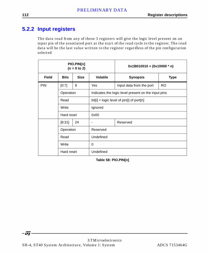
112 Register descriptionsPRELIMINARY DATA
5.2.2 Input registers
The data read from any of these 3 registers will give the logic level present on an input pin of the associated port at the start of the read cycle to the register. The read data will be the last value written to the register regardless of the pin configuration selected
PIO.PIN[n](n = 0 to 2)
0x1B010010 + (0x10000 * n)
Field Bits Size Volatile Synopsis Type
PIN [0:7] 8 Yes Input data from the port RO
Operation Indicates the logic level present on the input pins
Read bit[i] = logic level of pin[i] of port[n]
Write Ignored
Hard reset 0x00
[8:31] 24 - Reserved
Operation Reserved
Read Undefined
Write 0
Hard reset Undefined
Table 58: PIO.PIN[n]
STMicroelectronicsSH-4, ST40 System Architecture, Volume 1: System ADCS 7153464G
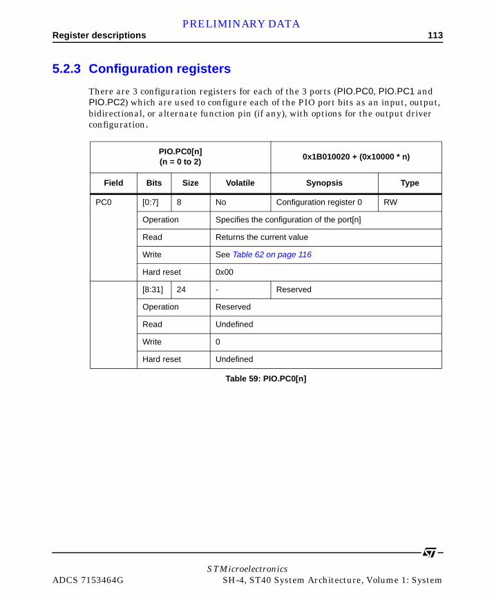
Register descriptions 113PRELIMINARY DATA
5.2.3 Configuration registers
There are 3 configuration registers for each of the 3 ports (PIO.PC0, PIO.PC1 and PIO.PC2) which are used to configure each of the PIO port bits as an input, output, bidirectional, or alternate function pin (if any), with options for the output driver configuration.
PIO.PC0[n] (n = 0 to 2)
0x1B010020 + (0x10000 * n)
Field Bits Size Volatile Synopsis Type
PC0 [0:7] 8 No Configuration register 0 RW
Operation Specifies the configuration of the port[n]
Read Returns the current value
Write See Table 62 on page 116
Hard reset 0x00
[8:31] 24 - Reserved
Operation Reserved
Read Undefined
Write 0
Hard reset Undefined
Table 59: PIO.PC0[n]
STMicroelectronicsADCS 7153464G SH-4, ST40 System Architecture, Volume 1: System
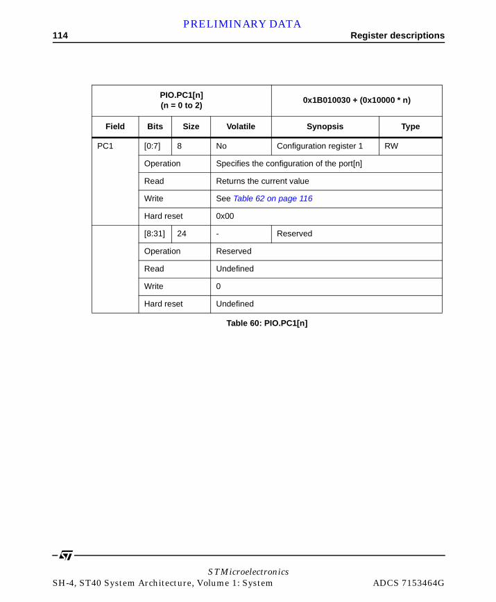
114 Register descriptionsPRELIMINARY DATA
PIO.PC1[n] (n = 0 to 2)
0x1B010030 + (0x10000 * n)
Field Bits Size Volatile Synopsis Type
PC1 [0:7] 8 No Configuration register 1 RW
Operation Specifies the configuration of the port[n]
Read Returns the current value
Write See Table 62 on page 116
Hard reset 0x00
[8:31] 24 - Reserved
Operation Reserved
Read Undefined
Write 0
Hard reset Undefined
Table 60: PIO.PC1[n]
STMicroelectronicsSH-4, ST40 System Architecture, Volume 1: System ADCS 7153464G
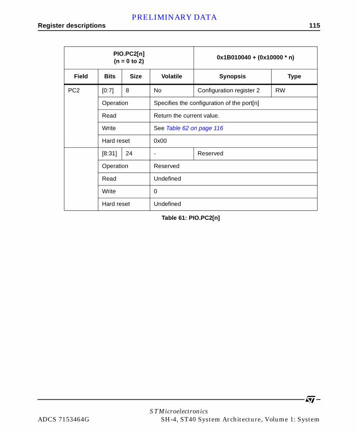
Register descriptions 115PRELIMINARY DATA
PIO.PC2[n](n = 0 to 2)
0x1B010040 + (0x10000 * n)
Field Bits Size Volatile Synopsis Type
PC2 [0:7] 8 No Configuration register 2 RW
Operation Specifies the configuration of the port[n]
Read Return the current value.
Write See Table 62 on page 116
Hard reset 0x00
[8:31] 24 - Reserved
Operation Reserved
Read Undefined
Write 0
Hard reset Undefined
Table 61: PIO.PC2[n]
STMicroelectronicsADCS 7153464G SH-4, ST40 System Architecture, Volume 1: System
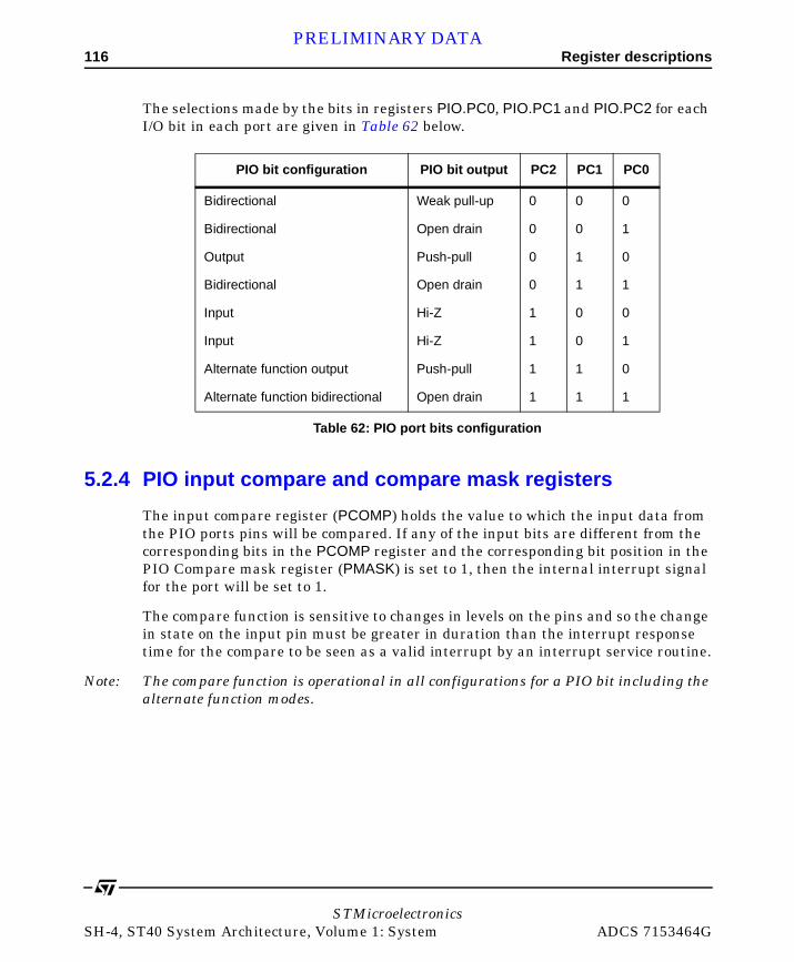
116 Register descriptionsPRELIMINARY DATA
The selections made by the bits in registers PIO.PC0, PIO.PC1 and PIO.PC2 for each I/O bit in each port are given in Table 62 below.
5.2.4 PIO input compare and compare mask registers
The input compare register (PCOMP) holds the value to which the input data from the PIO ports pins will be compared. If any of the input bits are different from the corresponding bits in the PCOMP register and the corresponding bit position in the PIO Compare mask register (PMASK) is set to 1, then the internal interrupt signal for the port will be set to 1.
The compare function is sensitive to changes in levels on the pins and so the change in state on the input pin must be greater in duration than the interrupt response time for the compare to be seen as a valid interrupt by an interrupt service routine.
Note: The compare function is operational in all configurations for a PIO bit including the alternate function modes.
PIO bit configuration PIO bit output PC2 PC1 PC0
Bidirectional Weak pull-up 0 0 0
Bidirectional Open drain 0 0 1
Output Push-pull 0 1 0
Bidirectional Open drain 0 1 1
Input Hi-Z 1 0 0
Input Hi-Z 1 0 1
Alternate function output Push-pull 1 1 0
Alternate function bidirectional Open drain 1 1 1
Table 62: PIO port bits configuration
STMicroelectronicsSH-4, ST40 System Architecture, Volume 1: System ADCS 7153464G

Register descriptions 117PRELIMINARY DATA
PIO.PCOMP[n] (n = 0 to 2)
0x1B010050 + (0x10000 * n)
Field Bits Size Volatile Synopsis Type
PCOMP [0:7] 8 Yes Input data from the port RO
Operation Indicates the logic level present on the input pins
Read bit[i] = logic level of pin[i] of port[n]
Write Ignored
Hard reset 0x00
[8:31] 24 - Reserved
Operation Reserved
Read Undefined
Write 0
Hard reset Undefined
Table 63: PIO.PCOMP[n]
PIO.PMASK[n](n = 0 to 2)
0x1B010060 + (0x10000 * n)
Field Bits Size Volatile Synopsis Type
PMask [0:7] 8 Yes Input data from the port RO
Operation Indicates the logic level present on the input pins
Read bit[i] = logic level of pin[i] of port[n]
Write Ignored
Hard reset 0x00
Table 64: PIO.PMASK[n]
STMicroelectronicsADCS 7153464G SH-4, ST40 System Architecture, Volume 1: System

118 Register descriptionsPRELIMINARY DATA
5.2.5 Pseudoregisters
Except for the PIO. PIN[N] register, all the PIO registers are each associated with a pair of pseudoregisters, at separate addresses, which allow individual bits within the register to be set or cleared.
These pseudoregisters are all of size 32-bits and write-only.
The PIO.SET pseudoregister allows bits to be set individually. Writing a 1 in this register sets the corresponding bit in the associated register, a 0 leaves the bit unchanged. The PIO.SET register is offset 4 bytes from its associated register.
The PIO.CLEAR pseudoregister allows bits to be cleared individually. Writing a 1 in this register resets the corresponding bit in the associated register, a 0 leaves the bit unchanged. The PIO.CLEAR register’s address is offset 8 bytes from its associated register’s address. These registers may only be accessed with aligned 32-bit loads and stores. The result of other accesses is undefined.
[8:31] 24 - Reserved
Operation Reserved
Read Undefined
Write 0
Hard reset Undefined
PIO.PMASK[n](n = 0 to 2)
0x1B010060 + (0x10000 * n)
Field Bits Size Volatile Synopsis Type
Table 64: PIO.PMASK[n]
STMicroelectronicsSH-4, ST40 System Architecture, Volume 1: System ADCS 7153464G
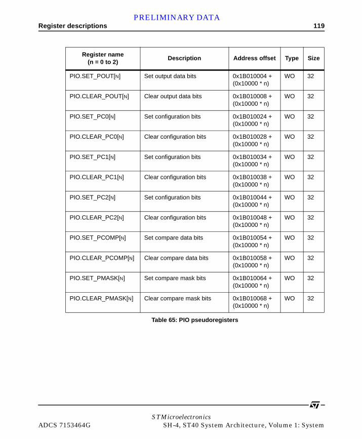
Register descriptions 119PRELIMINARY DATA
Register name(n = 0 to 2)
Description Address offset Type Size
PIO.SET_POUT[N] Set output data bits 0x1B010004 + (0x10000 * n)
WO 32
PIO.CLEAR_POUT[N] Clear output data bits 0x1B010008 + (0x10000 * n)
WO 32
PIO.SET_PC0[N] Set configuration bits 0x1B010024 + (0x10000 * n)
WO 32
PIO.CLEAR_PC0[N] Clear configuration bits 0x1B010028 + (0x10000 * n)
WO 32
PIO.SET_PC1[N] Set configuration bits 0x1B010034 + (0x10000 * n)
WO 32
PIO.CLEAR_PC1[N] Clear configuration bits 0x1B010038 + (0x10000 * n)
WO 32
PIO.SET_PC2[N] Set configuration bits 0x1B010044 + (0x10000 * n)
WO 32
PIO.CLEAR_PC2[N] Clear configuration bits 0x1B010048 + (0x10000 * n)
WO 32
PIO.SET_PCOMP[N] Set compare data bits 0x1B010054 + (0x10000 * n)
WO 32
PIO.CLEAR_PCOMP[N] Clear compare data bits 0x1B010058 + (0x10000 * n)
WO 32
PIO.SET_PMASK[N] Set compare mask bits 0x1B010064 + (0x10000 * n)
WO 32
PIO.CLEAR_PMASK[N] Clear compare mask bits 0x1B010068 + (0x10000 * n)
WO 32
Table 65: PIO pseudoregisters
STMicroelectronicsADCS 7153464G SH-4, ST40 System Architecture, Volume 1: System

120 Register descriptionsPRELIMINARY DATA
STMicroelectronicsSH-4, ST40 System Architecture, Volume 1: System ADCS 7153464G

PRELIMINARY DATA
STMicroelectroniADCS 7153464G SH-4, ST40 S
6ment
Clock and power manage
6.1 OverviewEach ST40 system contains a clock controller macro which is used to control the clocking, power-down and watchdog timers in the system.
These are organized as below.
• One or more clock generators (CPG/CLOCKGEN) each of which supports up to ten clock domains derived from two independently controllable PLLs.
• A power management unit (PMU) used to control the power and clocking status for on-chip modules or systems which may be used to disable clocks to specific modules.
• A watchdog timer (WDT) which triggers specific functions following periods of inactivity such as frequency resynchonizations or soft reset conditions.
The first clock controller block, referred to as CLOCKGEN A, controls the PMU and WDT features in addition to its own clock domains. The clocks associated with this block are labelled A11 though A15, A2M and A21 through A25 respectively.
Further CLOCKGEN blocks, if present, are referred to as CLOCKGEN B,C,D and so on. Each block has control clock domains labelled from 11 through 25, as for CLOCKGEN A. The blocks may also be allocated some PMU functionality.
This chapter discusses the general organization and architecture common to all ST40 systems. However, specific details may vary on some platforms, and the information presented here may be superseded by the product datasheet.
Details of a specific system’s clock and power management organization are available in the product datasheet.
csystem Architecture, Volume 1: System

122 Address mapPRELIMINARY DATA
6.2 Address mapThe address map is divided into a number of regions, a single CPG region which is always associated with CLOCKGEN A, and one or more CLKGEN regions associated with each CLOCKGEN bank. These are labeled CLKGEN[n] where n refers to the bank number A, B, C and so on.
A single bank of four registers controls the CPG block with a separate register bank for each CLOCKGEN block. The base addresses for each register bank is shown in the datasheet.
Some instances of a CLOCKGEN block may not use the full functionality available, so some registers may be reserved and some functions restricted. See the product datasheet for details.
6.2.1 CPG bank
CPG bank registers are mapped in the ST40 CPU core area starting at the base address given in the system address map.
Name Description TypeAddress
offsetAccess
size
CPG.FRQCR Frequency control register, seeSection 6.3.4.1
RW 0x00 16
CPG.STBCR Standby control register, see Section 6.5.4.1
RW 0x04 8
CPG.WTCNT Watchdog timer counter, see Section 6.4.3.1
RW 0x08 R:8, W:16
CPG.WTCSR Watchdog timer status register, seeSection 6.4.3.2
RW 0x0C R:8, W:16
CPG.STBCR2 Standby control register 2, seeSection 6.5.4.2
RW 0x10 8
CPG.FRQCR2
Frequency control register 2 is not implemented on ST40 devices.
- 0xC0 16
Table 66: CPGL bank registers
STMicroelectronicsSH-4, ST40 System Architecture, Volume 1: System ADCS 7153464G

Address map 123PRELIMINARY DATA
These registers except for CPG.FRQCR2 are common to all ST40 and SH-4 variants produced by Hitachi and ST and control features with a direct impact on the CPU such as the CPU clock frequency, and system watchdog behavior.
6.2.2 CLKGEN bank
Each CLOCKGEN block has a dedicated register bank to control its function. If there is more than one CLOCKGEN block in an ST40 implementation then each block and registers functions independently.
Each register is offset from the base address of the CLOCKGEN bank given in the system address map.
Register name
where n = [A:Z]Description Type
Address offset
bank [N]
Access size
CLKGEN[N].PLL1CR1 PLL1 control reg 1, see Section 6.3.4.2
Other 0x00 32
CLKGEN[N].PLL1CR2 PLL1 control reg2, see Section 6.3.4.3
RW 0x08 32
CLKGEN[N].PLL2CR PLL2 control register, see Section 6.3.4.4
RW 0x10 32
CLKGEN[N].STBREQCR Standby module req, see Section 6.5.4.1
RW 0x18 32
CLKGEN[N].STBREQCR_SET Set Standby module req, see Section 6.5.4.3
RW 0x20 32
CLKGEN[N].STBREQCR_CLR Clear Standby module req, see Section 6.5.4.3
RW 0x28 32
CLKGEN[N].STBACKCR Standby module ack, see Section 6.5.4.4
RW 0x30 32
CLKGEN[N].CLK4CR Clk4 control register selects the proper ratio for pll1_clk4, see Section 6.3.4.5
RW 0x38 32
Table 67: CLOCKGEN bank registers
STMicroelectronicsADCS 7153464G SH-4, ST40 System Architecture, Volume 1: System

124 Address mapPRELIMINARY DATA
CLKGEN[N].CPG_BYPASS when 1 set by-pass of ratio hardware filtering inside CLOCKGEN, see Section 6.3.4.6
RW 0x40 32
CLKGEN[N].PLL2_MUXCR Pll2_mux_clk control reg Selects the proper ratio for pll2_mux_clk, see Section 6.3.4.7
RW 0x48 32
CLKGEN[N].CLK1CR Clk1 control register selects the proper ratio for pll1_clk1 when CPG_BYPASS is set to 1, see Section 6.3.4.8
RW 0x50 32
CLKGEN[N].CLK2CR Clk2 control register selects the proper ratio for pll1_clk2 when CPG_BYPASS is set to 1, see Section 6.3.4.9
RW 0x58 32
CLKGEN[N].CLK3CR Clk3 control register selects the proper ratio for pll1_clk3 when CPG_BYPASS is set to 1, see Section 6.3.4.10
RW 0x60 32
CLKGEN[N].CLK_SELCR External mux clock selection Control reg. (Control to CLOCKCON) see Section 6.3.4.11
RW 0x68 32
Register name
where n = [A:Z]Description Type
Address offset
bank [N]
Access size
Table 67: CLOCKGEN bank registers
STMicroelectronicsSH-4, ST40 System Architecture, Volume 1: System ADCS 7153464G

Clock functionality 125PRELIMINARY DATA
6.3 Clock functionality
6.3.1 Internal organization
The internal organization of each clock controller is shown in Figure 14.
Figure 13: CLOCKGEN architecture
GCK
Clock domain A11
Clock domain A12
Clock domain A13
Clock Domain A21
Clock Domain A22
Clock Domain A2M
Clock Domain A24
Clock Domain A25
Clock Domain A23
ST40-CLOCKGEN27 MHz
PLL1div 1/2
x1x2
x2/3x3x4x6x8
Clock domain A14
RATIOFILTER
PLL2
: 11
: 4
: 8
: 16
Dividersbank 2
: 21
PLL1CR1PLL1CR2
CPG_BYPASSCLK1CR
CLK2CRCLK3CR
CLK4CR
ratio
clkstop
PLL2_MUXCRPLL2CR
STBREQCR
STBACKCR
pwr_down_req [7:0]
pwr_down_ack[7:0]
CLK_SELCR
clk_sel [7:0]STBus
main_1clk
main_2clk
Dividersbank1
CPGL
FRQCR
FRQCR2
STBCR2
STBCR
CLOCKGEN bank
Bank
XTAL in
CLOCKGEN A only
STMicroelectronicsADCS 7153464G SH-4, ST40 System Architecture, Volume 1: System
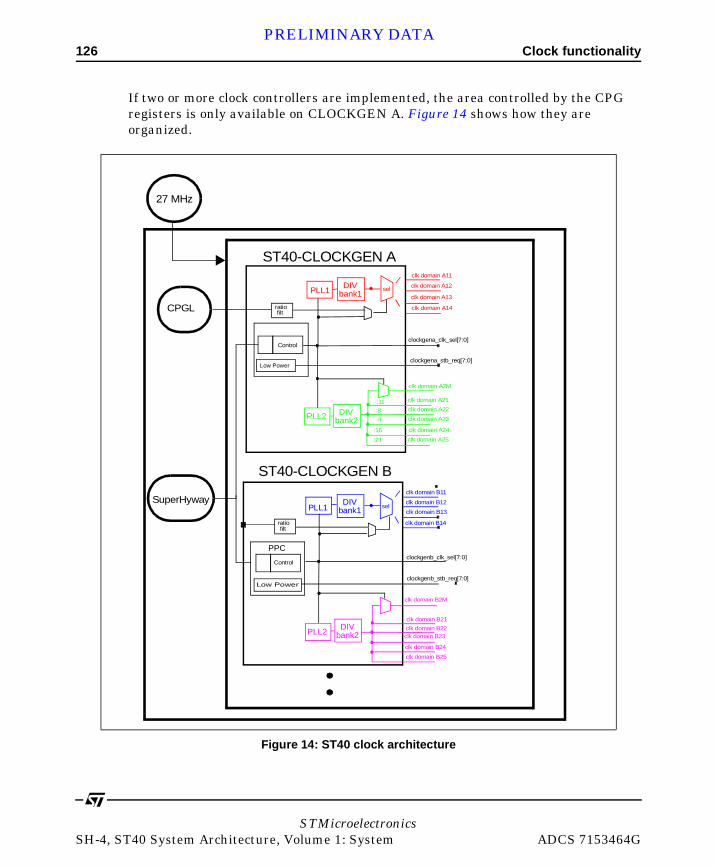
126 Clock functionalityPRELIMINARY DATA
If two or more clock controllers are implemented, the area controlled by the CPG registers is only available on CLOCKGEN A. Figure 14 shows how they are organized.
Figure 14: ST40 clock architecture
PLL1
PLL2
DIVclk domain A11
clk domain A12
clk domain A13
clk domain A14
selbank1
DIVbank2
clk domain A22
clk domain A23
clk domain A24
clk domain A2M
clk domain A21
clk domain A25
ratiofilt
Control
PLL1
PLL2
DIVclk domain B11
clk domain B12
clk domain B13
clk domain B14
selbank1
DIVbank2
clk domain B22clk domain B23
clk domain B24
clk domain B2M
clk domain B21
clk domain B25
ratiofilt
Control
PPC
Low Power
CPGL
:11
:4
:8
:16
:21
SuperHyway
ST40-CLOCKGEN A
ST40-CLOCKGEN B
clockgenb_clk_sel[7:0]
clockgena_stb_req[7:0]
clockgena_clk_sel[7:0]
clockgenb_stb_req[7:0]
27 MHz
Low Power
STMicroelectronicsSH-4, ST40 System Architecture, Volume 1: System ADCS 7153464G
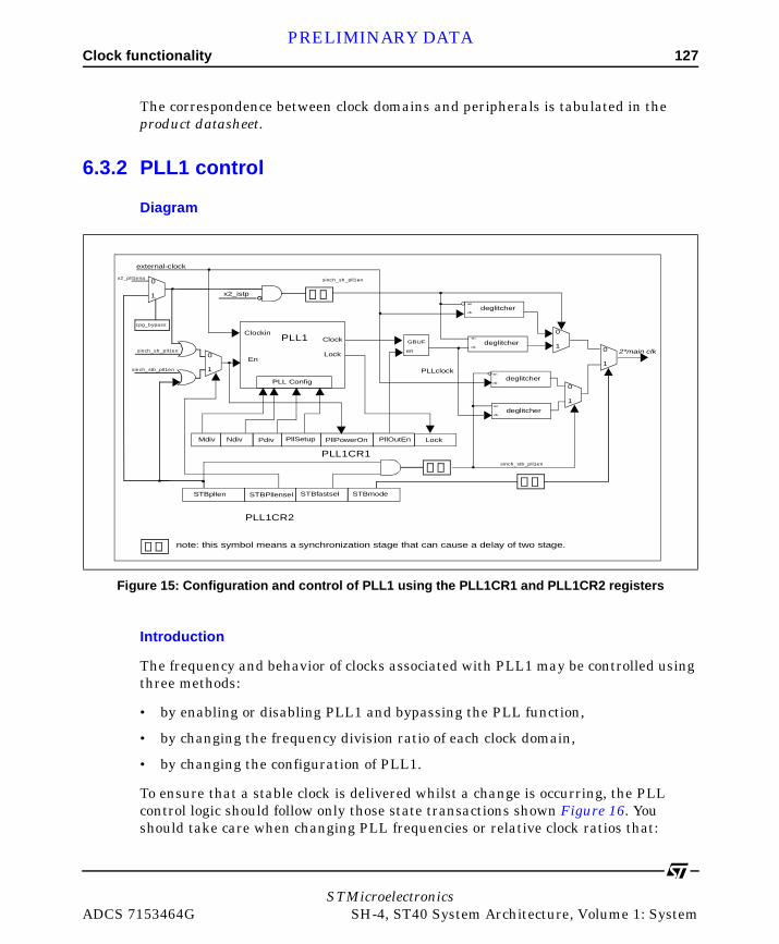
Clock functionality 127PRELIMINARY DATA
The correspondence between clock domains and peripherals is tabulated in the product datasheet.
6.3.2 PLL1 control
Diagram
Introduction
The frequency and behavior of clocks associated with PLL1 may be controlled using three methods:
• by enabling or disabling PLL1 and bypassing the PLL function,
• by changing the frequency division ratio of each clock domain,
• by changing the configuration of PLL1.
To ensure that a stable clock is delivered whilst a change is occurring, the PLL control logic should follow only those state transactions shown Figure 16. You should take care when changing PLL frequencies or relative clock ratios that:
Figure 15: Configuration and control of PLL1 using the PLL1CR1 and PLL1CR2 registers
PLL1
Mdiv Ndiv
PLL1CR1
Pdiv PllSetup PllPowerOn
PLL Config
EnLock
Clock
PllOutEn
en
GBUF
0
1
Lock
PLLclock
Clockin
external-clock
2*main clk
x2_pll1ena
0
10
1
STBpllen
PLL1CR2
STBPllensel STBfastsel
deglitcherclk
en
deglitcherclk
en
deglitcherclk
en
0
1
STBmode
note: this symbol means a synchronization stage that can cause a delay of two stage.
x2_istp
sinch_sh_pll1en
sinch_sh_pll1en
sinch_stb_pll1en
sinch_stb_pll1en
deglitcherclk
en
0
1
cpg_bypass
STMicroelectronicsADCS 7153464G SH-4, ST40 System Architecture, Volume 1: System

128 Clock functionalityPRELIMINARY DATA
• the PLL is stable before re-enabling clocks,
• there is no communications traffic between semi-synchronous domains when changing relative clock ratios.
The PLL frequency is defined by the contents of the MDIV, NDIV and PDIV in the CLKGEN.PLL1CR1 register. For details of allowable values refer to the datasheet.
Allowable transitions
States labelled sh_xxx are available for CLOCKGEN A only,
States labeled st_xxx are available for all CLOCKGEN macros.
Figure 16: CLOCKGEN A PLL1 valid states
sh_run_slow
st_leaving_slow
start-up (mode 0 to 5)
program PLL1CR1(PLL dividers)
after PLL locked
program PLL1CR1
and CPGL-WDT(PLL dividers)
_fast: clock source is PLL1_slow: clock source is external xosc @ 27 MHz
sh2st_slow
st2sh_slow
st2sh_fast
sh2st_fast
sh_: control by FRQCRst_: control by PLL1CR2
ratio encodedratio encoded
cpg_bypass=0cpg_bypass=0
st_run_slow
ratio encodedcpg_bypass=0
st_run_fast
ratio encodedcpg_bypass=0
sh_run_fast
no ratio encodedcpg_bypass=1
start-up (mode 6 & 7)
CLOCKGEN PLL1 valid states(related to PLL1)
no ratio encodedcpg_bypass=1
STMicroelectronicsSH-4, ST40 System Architecture, Volume 1: System ADCS 7153464G
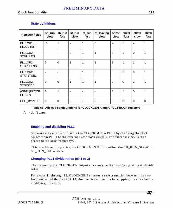
Clock functionality 129PRELIMINARY DATA
State definitions
Enabling and disabling PLL1
Software may enable or disable the CLOCKGEN A PLL1 by changing the clock source from PLL1 to the external xosc clock directly. The internal clock is then preset to the xosc frequency/2.
This is achieved by placing the CLOCKGEN PLL in either the SH_RUN_SLOW or ST_RUN_SLOW state.
Changing PLL1 divide ratios (clk1 to 3)
The frequency of a CLOCKGEN output clock may be changed by updating its divide ratio.
For clocks 11 through 13, CLOCKGEN ensures a safe transition between the two frequencies, whilst for clock 14, the user is responsible for stopping the clock before modifying the ratios.
Register fieldssh_run slow
sh_run fast
st_run slow
st_run fast
st_leaving slow
sh2st slow
sh2st fast
st2sh slow
st2sh fast
PLL1CR1.PLLOUTEN
-A
A. - don’t care
1 - 1 0 - 1 - 1
PLL1CR2.STBPLLEN
- - 0 1 1 0 1 0 1
PLL1CR2.STBPLLENSEL
0 0 1 1 1 1 1 1 1
PLL1CR2.STFASTSEL
- - 0 1 0 0 1 0 1
PLL1CR2.STBMODE
0 0 1 1 1 0 0 1 1
(CPGL)FRQCR.PLL1EN
0 1 - - - 0 1 0 1
CPG_BYPASS 0 0 - - 0 0 0 0 0
Table 68: Allowed configurations for CLOCKGEN A and CPGL.FRQCR registers
STMicroelectronicsADCS 7153464G SH-4, ST40 System Architecture, Volume 1: System

130 Clock functionalityPRELIMINARY DATA
Whilst the transition is guaranteed for clocks 11 through 13, the user must ensure the target module functions correctly during this period. Some modules such as UARTs require stable frequencies during operation. Others are associated with more than one clock and are unable to function correctly if the ratio between those clocks changes whilst the module is active.
Restrictions may apply. As an example, in some ST40 systems, the CPU has direct dependencies on two clock domains, I-Clk and P-Clk. Changes in relative frequency between these clocks whilst the CPU is active may lead to undefined behavior. For the ST40 CPU, I-Clk must be an integer multiple of the P-Clk frequency. The maximum supported frequencies are in the product datasheet.
Two methods are supported for changing PLL1 divide ratios.
• CPGL mode (allowed only for CLOCKGEN A clocks)
If CLKGEN.CPG_BYPASS is inactive (set to 0), CLOCKGEN A is in CPGL mode. The frequency of clocks 11 through 13 may be changed by reprogramming CPG.FRQCR. CPGL mode is the default for CLOCKGEN A clocks.
• ST mode
If CLKGEN.CPG_BYPASS is active (set to 1), the CLOCKGEN macro is in ST mode. The frequency of clocks 11 through 13 may be changed by programming CLKGEN.CLK1CR, CLKGEN.CLK2CR and CLKGEN.CLK3CR respectively.
Changing the PLL1 divide ratio for clock 14
The frequency of clock 14 may be changed by updating the CLKGEN.CLK4CR register. The following procedure ensures safe operation.
1 Stop clock 14 by asserting (setting to 1) CLKGEN.CLK4CR.CLKSTOP.
2 Change the field ratio of CLKGEN.CLK4CR.
3 Restart clock 14 by de-asserting (setting to 0) CLKGEN.CLK4CR.CLKSTOP.
Changing PLL1 lock frequency
The ST40 CLOCKGEN macro includes a highly flexible PLL which may be programmed to output a range of frequencies. This is achieved by updating the MDIV, NDIV and PDIV fields of CLKGEN.PLL1CR1. However whilst the PLL is locking-on the new frequency, the clock outputted by the macro is unstable. Software should ensure there is no activity in parts of the system associated with the PLL. There are two methods of handling this. You can either put the system to
STMicroelectronicsSH-4, ST40 System Architecture, Volume 1: System ADCS 7153464G

Clock functionality 131PRELIMINARY DATA
sleep, and use the watchdog to restart the system when the PLL clocks are stable, or bypass the PLL and use an external clock during the period of instability.
Examples of these procedures are described below.
SH procedure: CLOCKGENA only
1 Move CLOCKGEN to state sh_run_slow.
This action disables the PLL1 and sets the CLOCKGEN clock source to the external crystal (27 MHz).
Note: the maximum clock rate is half of the input clock rate (see Figure 14 and Figure 15).
2 Update PLL1 using the MDIV, NDIV and PDIV fields of CLKGEN.PLL1CR1.
Only values defined in the datasheet are valid, other values may lead to undefined behavior.
3 Program the WDT to provide the specified oscillation stabilization time before timing out.
The WDT should have the following settings:
CPG.WTCSR register: TME bit = 0, WDT stopped,
CPG.WTCSR register: CKS2 to CKS0 bits, WDT count clock division ratio,
CPG.WTCNT register: initial counter value,
CPG.WTCNT register: initial counter value.
4 Move CLOCKGEN to STATE sh_run_fast.
This puts the CPU in a suspend state until the WDT countdown completes, at which point the PLL is re-enabled and clocks 11 through 14 are restarted using the new PLL frequency.
ST procedure
1 Move CLOCKGEN to state st_run_slow.
This action disables PLL1 and selects the external crystal clock as the input to the system bypassing PLL1. The internal clock frequency is a divisor of half the external clock ratio as determined by the clock 11 through 14 divide ratios.
2 Update PLL1 using the MDIV, NDIV and PDIV fields of CLKGEN.PLL1CR1.
Only values defined in the datasheet are valid, other values may lead to undefined behavior.
STMicroelectronicsADCS 7153464G SH-4, ST40 System Architecture, Volume 1: System

132 Clock functionalityPRELIMINARY DATA
3 Move CLOCKGEN to state st_leaving_slow.
PLL1 is enabled, but is still bypassed.
4 Wait for PLL1CR1.LOCK to reach 1.
This indicates the PLL has stabilized.
5 Move CLOCKGEN to state st_run_fast.
The clock source for clocks 11 through 14 to the PLL is changed rather than the external x-tal clock.
Note: no clocks are stopped using the ST procedure.
PLL frequency calculation
Details of the relationship between CLKGEN.PLL1CR1.[MDIV, NDIV, PDIV] and the PLL frequency are available in the product datasheet.
6.3.3 Configuring PLL2
Introduction
Figure 17: Configuration and control of PLL2 using the PLL2CR registers
PLL2
Mdiv Ndiv Pdiv PllSetup PllPowerOn
PLL ConfigEn
Lock
Clock
PllOutEn
en
GBUF
LockSelect
0
1
Lock
PLLclockClockinexternal-clock1
0
pci_host
pci_clkin
PCIclock
STMicroelectronicsSH-4, ST40 System Architecture, Volume 1: System ADCS 7153464G

Clock functionality 133PRELIMINARY DATA
There are two ways of changing the frequency of clocks associated with the PLL2 clock:
• enabling or disabling PLL2,
• changing the configuration of PLL2.
The procedures are discussed below, for details on specific PLL settings refer to the datasheet for that device.
Procedure to enable and disable PLL2
CLOCKGEN PLL2 is disabled by writing 0 to CLKGEN.PLL2CR.PLLOUTEN and CLKGEN.PLL2CR.LOCKSELECT.
It is enabled by writing 1 to CLKGEN.PLL2CR.PLLOUTEN and CLKGEN.PLL2CR.LOCKSELECT.
In some systems it may be possible to bypass PLL2, see datasheet for details.
Changing the frequency of PLL2
The PLL2 derived clocks are generated by CLOCKGEN using PLL2 which is a programmable PLL.
PLL2 takes the input frequency from the external qx_xtalout27 clock, which runs at 27 MHz. It is possible to change the output frequency of this PLL by changing the value of its MDIV, NDIV and PDIV. This can be achieved programming the corresponding fields of the configuration register PLL2CR.
To change the PLL2 output frequency to a value different from at start up, use the following procedure.
1 Write 0 in the PLL2CR register fields PLLOUTEN and LOCKSELECT.
This allows CLOCKGEN to stop the PLL2 clockout (PLL2 clock = 0).
2 Disable PLL2 by setting PLL2CR.PLLPOWERON to 0.
3 Change the division and multiply ratios of PLL2 by updating the values of the MDIV, NDIV and PDIV fields of the PLL2CR register, as defined by the datasheet.
4 Restart PLL2 by setting PLL2CR.PLLPOWERON to 1.
5 Set the LOCKSELECT field of PLL2CR to 1 to enable output of the PLL2 clock when the lock is achieved.
STMicroelectronicsADCS 7153464G SH-4, ST40 System Architecture, Volume 1: System
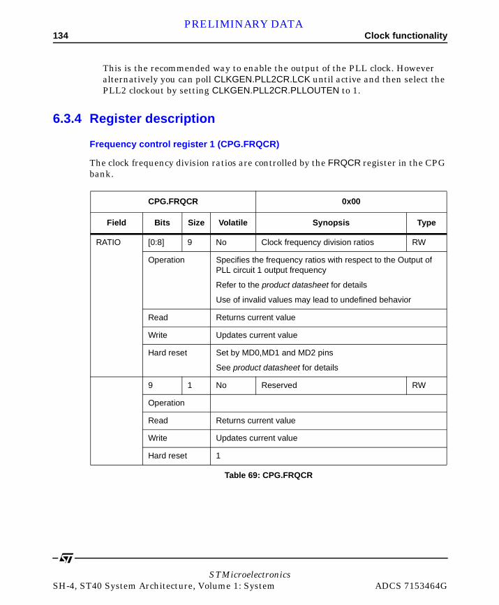
134 Clock functionalityPRELIMINARY DATA
This is the recommended way to enable the output of the PLL clock. However alternatively you can poll CLKGEN.PLL2CR.LCK until active and then select the PLL2 clockout by setting CLKGEN.PLL2CR.PLLOUTEN to 1.
6.3.4 Register description
Frequency control register 1 (CPG.FRQCR)
The clock frequency division ratios are controlled by the FRQCR register in the CPG bank.
CPG.FRQCR 0x00
Field Bits Size Volatile Synopsis Type
RATIO [0:8] 9 No Clock frequency division ratios RW
Operation Specifies the frequency ratios with respect to the Output of PLL circuit 1 output frequency
Refer to the product datasheet for details
Use of invalid values may lead to undefined behavior
Read Returns current value
Write Updates current value
Hard reset Set by MD0,MD1 and MD2 pins
See product datasheet for details
9 1 No Reserved RW
Operation
Read Returns current value
Write Updates current value
Hard reset 1
Table 69: CPG.FRQCR
STMicroelectronicsSH-4, ST40 System Architecture, Volume 1: System ADCS 7153464G
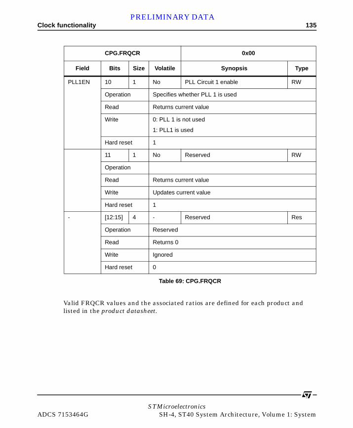
Clock functionality 135PRELIMINARY DATA
Valid FRQCR values and the associated ratios are defined for each product and listed in the product datasheet.
PLL1EN 10 1 No PLL Circuit 1 enable RW
Operation Specifies whether PLL 1 is used
Read Returns current value
Write 0: PLL 1 is not used
1: PLL1 is used
Hard reset 1
11 1 No Reserved RW
Operation
Read Returns current value
Write Updates current value
Hard reset 1
- [12:15] 4 - Reserved Res
Operation Reserved
Read Returns 0
Write Ignored
Hard reset 0
CPG.FRQCR 0x00
Field Bits Size Volatile Synopsis Type
Table 69: CPG.FRQCR
STMicroelectronicsADCS 7153464G SH-4, ST40 System Architecture, Volume 1: System

136 Clock functionalityPRELIMINARY DATA
CLKGEN.PLL1CR1
This register defines the behavior of PLL 1.
CLOCKGEN.PLL1CR1
PLL1 control Register0x00
Field Bits Size Volatile Synopsis Type
MDIV [0:7] 8 - Pre-divider Other
Operation Parameter for programming PLL1
Read Returns current value
Write Updates current value
Note: this register has a write lockA
Only certain values, as defined in the product datasheet, may be written. All other values are reserved and give undefined behavior.
Hard reset See datasheet
NDIV [8:15] 8 - Feedback divider Other
Operation Parameter for programming PLL1
Read Returns current value
Write Updates current value
Note: this register has a write lock A
Only certain values, as defined in the product datasheet, may be written. All other values are reserved and give undefined behavior.
Hard reset See the product datasheet
Table 70: CLOCKGEN.PLL1CR1
STMicroelectronicsSH-4, ST40 System Architecture, Volume 1: System ADCS 7153464G

Clock functionality 137PRELIMINARY DATA
PDIV [16:18] 3 - Post divider Other
Operation Parameter for programming PLL1
Read Returns current value
Write Updates current value
Note: this register has a write lockA
Only certain values, as defined in the product datasheet, may be written. All other values are reserved and give undefined behavior.
Hard reset See datasheet
SETUP [19:27] 9 - Loop characteristics Other
Operation Parameter for programming PLL1
Read Returns current value
Write Updates current value
Note: this register has a write lockA
Only certain values, as defined in the product datasheet, may be written. All other values are reserved and give undefined behavior.
Hard reset See datasheet
POWERON 28 1 - PLL1 Power On RO
Operation Specifies the power setting of PLL1
Read 1: power on
0: power off
Write Ignored
Hard reset See the product datasheet
CLOCKGEN.PLL1CR1
PLL1 control Register0x00
Field Bits Size Volatile Synopsis Type
Table 70: CLOCKGEN.PLL1CR1
STMicroelectronicsADCS 7153464G SH-4, ST40 System Architecture, Volume 1: System
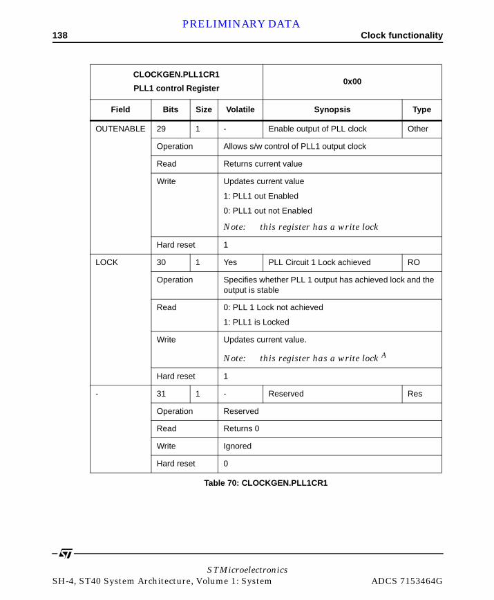
138 Clock functionalityPRELIMINARY DATA
OUTENABLE 29 1 - Enable output of PLL clock Other
Operation Allows s/w control of PLL1 output clock
Read Returns current value
Write Updates current value
1: PLL1 out Enabled
0: PLL1 out not Enabled
Note: this register has a write lock
Hard reset 1
LOCK 30 1 Yes PLL Circuit 1 Lock achieved RO
Operation Specifies whether PLL 1 output has achieved lock and the output is stable
Read 0: PLL 1 Lock not achieved
1: PLL1 is Locked
Write Updates current value.
Note: this register has a write lock A
Hard reset 1
- 31 1 - Reserved Res
Operation Reserved
Read Returns 0
Write Ignored
Hard reset 0
CLOCKGEN.PLL1CR1
PLL1 control Register0x00
Field Bits Size Volatile Synopsis Type
Table 70: CLOCKGEN.PLL1CR1
STMicroelectronicsSH-4, ST40 System Architecture, Volume 1: System ADCS 7153464G

Clock functionality 139PRELIMINARY DATA
CLKGEN.PLL1CR2
This register defines the behavior of PLL 1.
A. CLOCKGEN.PLL1CR1 is writable if (PLL1CR2.STBPLLENSEL = 0 and FRQCR.PLL1EN = 0) or (PLL1CR2.STBPLLENSEL= 1 andPLL1CR2.STBPLLEN = 0)
CLOCKGEN.PLL1CR2
PLL1 control Register0x08
Field Bits Size Volatile Synopsis Type
STBPLLEN 0 1 - PLL1 enable RW
Operation Alternative enable to the FRQCR.PLL1EN field See Figure 15
This field specifies whether PLL1 is enabled when STBPLLENSEL is 1, otherwise it has no effect
Read Returns current value
Write 1: enabled
0: not enabled AND selected the external-clock as input clock
Hard reset 0
Table 71: CLOCKGEN.PLL1CR2
STMicroelectronicsADCS 7153464G SH-4, ST40 System Architecture, Volume 1: System

140 Clock functionalityPRELIMINARY DATA
STBPLLENSEL
1 1 - PLL1 enable selector. RW
Operation Selects if PLL1 is enabled by FRQCR.PLL1EN or STBPLLEN.
See Figure 15
Read Returns current value
Write Updates current value
0: FRQCR.PLL1EN specifies enablingA
1: STBPLLEN specifies enabling
Hard reset 0
STBFASTSEL
2 1 - Clock selector RW
Operation Select if 2*main clock is set to PLL1_CLOCK (fast) or to external clock from the xtal.
The switch is synchronized
Note: Selection take place only if STBMODE field is set to 1 see Figure 15
Read Returns current value
Write Updates current value
1: 2*main_clock equal to PLL1 clock (fast clock)
0: 2*main_clock equal to external clock
Hard reset 0
CLOCKGEN.PLL1CR2
PLL1 control Register0x08
Field Bits Size Volatile Synopsis Type
Table 71: CLOCKGEN.PLL1CR2
STMicroelectronicsSH-4, ST40 System Architecture, Volume 1: System ADCS 7153464G
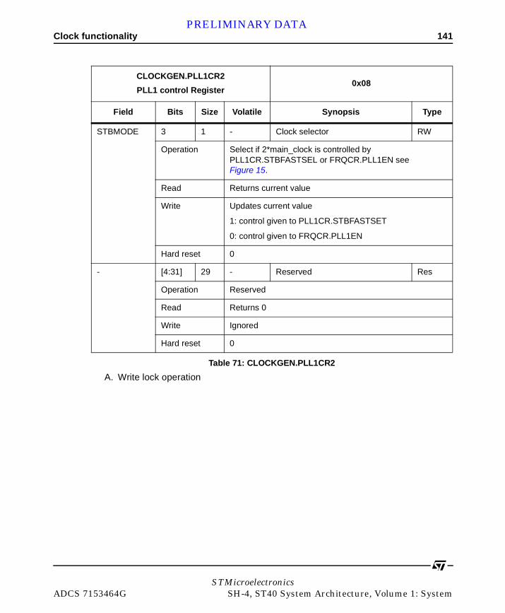
Clock functionality 141PRELIMINARY DATA
STBMODE 3 1 - Clock selector RW
Operation Select if 2*main_clock is controlled by PLL1CR.STBFASTSEL or FRQCR.PLL1EN see Figure 15.
Read Returns current value
Write Updates current value
1: control given to PLL1CR.STBFASTSET
0: control given to FRQCR.PLL1EN
Hard reset 0
- [4:31] 29 - Reserved Res
Operation Reserved
Read Returns 0
Write Ignored
Hard reset 0
A. Write lock operation
CLOCKGEN.PLL1CR2
PLL1 control Register0x08
Field Bits Size Volatile Synopsis Type
Table 71: CLOCKGEN.PLL1CR2
STMicroelectronicsADCS 7153464G SH-4, ST40 System Architecture, Volume 1: System
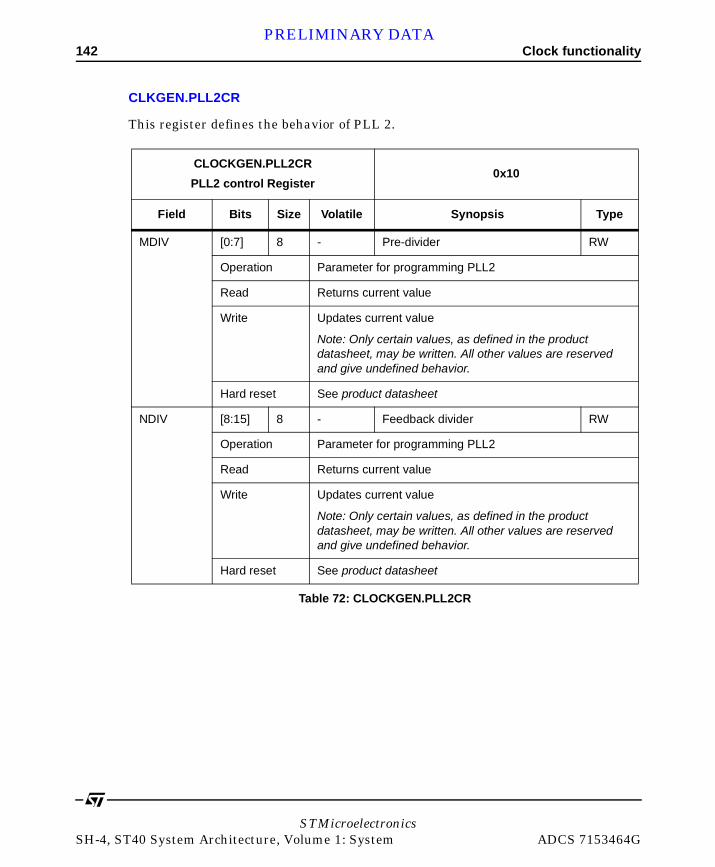
142 Clock functionalityPRELIMINARY DATA
CLKGEN.PLL2CR
This register defines the behavior of PLL 2.
CLOCKGEN.PLL2CR
PLL2 control Register0x10
Field Bits Size Volatile Synopsis Type
MDIV [0:7] 8 - Pre-divider RW
Operation Parameter for programming PLL2
Read Returns current value
Write Updates current value
Note: Only certain values, as defined in the product datasheet, may be written. All other values are reserved and give undefined behavior.
Hard reset See product datasheet
NDIV [8:15] 8 - Feedback divider RW
Operation Parameter for programming PLL2
Read Returns current value
Write Updates current value
Note: Only certain values, as defined in the product datasheet, may be written. All other values are reserved and give undefined behavior.
Hard reset See product datasheet
Table 72: CLOCKGEN.PLL2CR
STMicroelectronicsSH-4, ST40 System Architecture, Volume 1: System ADCS 7153464G
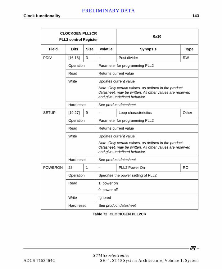
Clock functionality 143PRELIMINARY DATA
PDIV [16:18] 3 - Post divider RW
Operation Parameter for programming PLL2
Read Returns current value
Write Updates current value
Note: Only certain values, as defined in the product datasheet, may be written. All other values are reserved and give undefined behavior.
Hard reset See product datasheet
SETUP [19:27] 9 - Loop characteristics Other
Operation Parameter for programming PLL2
Read Returns current value
Write Updates current value
Note: Only certain values, as defined in the product datasheet, may be written. All other values are reserved and give undefined behavior.
Hard reset See product datasheet
POWERON 28 1 - PLL2 Power On RO
Operation Specifies the power setting of PLL2
Read 1: power on
0: power off
Write Ignored
Hard reset See product datasheet
CLOCKGEN.PLL2CR
PLL2 control Register0x10
Field Bits Size Volatile Synopsis Type
Table 72: CLOCKGEN.PLL2CR
STMicroelectronicsADCS 7153464G SH-4, ST40 System Architecture, Volume 1: System

144 Clock functionalityPRELIMINARY DATA
PLLOUTEN 29 1 - Enable output of PLL2 clock RW
Operation Allows s/w control of PLL2 output clock
Read Returns current value
Write Updates current value
1: PLL out Enabled
0: PLL out not Enabled
Hard reset See product datasheet
LOCKSELECT
30 1 Yes Selects how the PLL2 is enabled RW
Operation Specifies whether PLL2 output should be enabled when lock is achieved or as indicated by PLLOUTEN field
Read Returns current value
Write 0: PLLOUTEN setting governs PLL2 output
1: Lock setting governs PLL PCIoutput
Hard reset See product datasheet
LOCK 31 1 Yes PLL2 Lock achieved RO
Operation Specifies whether PLL2 output has achieved lock and the output is stable
Read 0: PLL2 Lock not achieved
1: PLL2 is Locked
Write Updates current value
Hard reset See product datasheet
CLOCKGEN.PLL2CR
PLL2 control Register0x10
Field Bits Size Volatile Synopsis Type
Table 72: CLOCKGEN.PLL2CR
STMicroelectronicsSH-4, ST40 System Architecture, Volume 1: System ADCS 7153464G

Clock functionality 145PRELIMINARY DATA
CLOCKGEN.CLK4CR
CLK4CR allows software to change the division ratio of this clock.
CLOCKGEN.CLK4CR
PLL1 Clock 4 control register0x38
Field Bits Size Volatile Synopsis Type
RATIO [0:2] 3 - Division ratio of PLL1CLK4 clock with respect of output of PLL1 div 2
RW
Operation
Read Returns current value
Write 000: ratio 1:1
001: ratio 1:2
010: ratio 1:3
011: ratio 2:3
100: ratio 1:4
101: ratio 1:6
110: ratio 1:8
111: ratio 1:8.
Hard reset see datasheet
CLKSTOP 3 1 - PLL1 enable selector. RW
Operation This bit allows stopping of the PLL1CLK4 clock
Read Returns current value
Write Updates current value
A0: PLL1CLK4 clock active
1: PLL1CLK4 clock stopped
Hard reset 0
Table 73: CLOCKGEN.CLK4CR
STMicroelectronicsADCS 7153464G SH-4, ST40 System Architecture, Volume 1: System

146 Clock functionalityPRELIMINARY DATA
To safely change the value of the division ratio of the PLL1CLK4 clock the following sequence should be followed:
1 Stop PLL1CLK4 clock by setting CLK4CR.CLKSTOP = 0
2 Write the new setting in CLK4CR.RATIO
3 Restart PLL1CLK4 clock by setting PLL1CLK4.CLKSTOP = 1
- [4:31] 28 - Reserved Res
Operation Reserved
Read Returns 0
Write Ignored
Hard reset 0
CLOCKGEN.CLK4CR
PLL1 Clock 4 control register0x38
Field Bits Size Volatile Synopsis Type
Table 73: CLOCKGEN.CLK4CR
STMicroelectronicsSH-4, ST40 System Architecture, Volume 1: System ADCS 7153464G

Clock functionality 147PRELIMINARY DATA
CLOCKGEN.CPGBYPASS
CLOCKGEN.CPGBYPASS
Field Bits Size Volatile Synopsis Type
BYPASS [0] 1 No master control source for clocks 11 - 13
RW
Operation 0: PLL1 clocks 1, 2, 3 controlled by CPG.FRQCR
1= PLL1 clocks controlled as below
CLKGEN.CLK1CR controls clock 11
CLKGEN.CLK2CR controls clock 12
CLKGEN.CLK3CR controls clock 13
Read Returns current value
Write Updated
Hard reset See product datasheet
- [1:31] 28 — Reserved Res
Operation Reserved
Read Reserved
Write 0: ignored, other values undefined
Hard reset 0
Table 74: CLOCKGEN.CPGBYPASS
STMicroelectronicsADCS 7153464G SH-4, ST40 System Architecture, Volume 1: System

148 Clock functionalityPRELIMINARY DATA
CLKGEN.PLL2_MUXCR
CLOCKGEN.PLL2_MUXCR
Field Bits Size Volatile Synopsis Type
MUXCTRL [1:0] 2 No Controls division ratio of clock 2M with respect to the output of PLL2
RW
Operation 00: Ratio 1:8
01: Ratio 1:16
10: Ratio 1:21
11: Ratio 1:1
Read Returns current value
Write Updates current value
Hard reset See product datasheet
- [2:31] 28 — Reserved Res
Operation Reserved
Read Reserved
Write 0: ignored, other values undefined
Hard reset 0
Table 75: CLOCKGEN.PLL2_MUXCR
STMicroelectronicsSH-4, ST40 System Architecture, Volume 1: System ADCS 7153464G

Clock functionality 149PRELIMINARY DATA
CLKGEN.CLK1CR
CLOCKGEN.CLK1CR
Field Bits Size Volatile Synopsis Type
RATIO [2:0] 2 No clock ratio control when CLKGEN.CPG_BYPASS active
RW
Operation Controls the ratio of clock with respect to PLL1 division 2
000: 1:1 100: 1:4
001: 1:2 101: 1:6
010: 1:3 110: 1:8
011: 2:3 111: 1:8
Read Returns current value
Write Updated
Hard reset See product datasheet
CLKSTOP [3] 1 No Clock 11 enable override RO
Operation 1: clock 11 disabled
0: clock 11 enabled
Read Returns current value
Write Updated
Hard reset See product datasheet
- [2:31] 28 - Reserved Res
Operation Reserved
Read Reserved
Write 0: ignored, other values undefined
Hard reset 0
Table 76: CLOCKGEN.CLK1CR
STMicroelectronicsADCS 7153464G SH-4, ST40 System Architecture, Volume 1: System
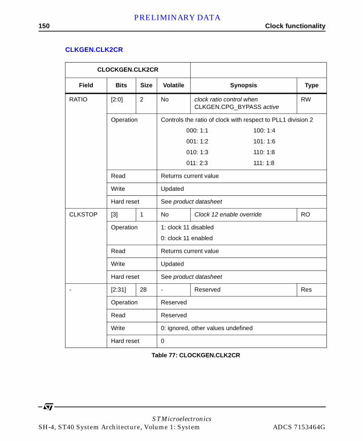
150 Clock functionalityPRELIMINARY DATA
CLKGEN.CLK2CR
CLOCKGEN.CLK2CR
Field Bits Size Volatile Synopsis Type
RATIO [2:0] 2 No clock ratio control when CLKGEN.CPG_BYPASS active
RW
Operation Controls the ratio of clock with respect to PLL1 division 2
000: 1:1 100: 1:4
001: 1:2 101: 1:6
010: 1:3 110: 1:8
011: 2:3 111: 1:8
Read Returns current value
Write Updated
Hard reset See product datasheet
CLKSTOP [3] 1 No Clock 12 enable override RO
Operation 1: clock 11 disabled
0: clock 11 enabled
Read Returns current value
Write Updated
Hard reset See product datasheet
- [2:31] 28 - Reserved Res
Operation Reserved
Read Reserved
Write 0: ignored, other values undefined
Hard reset 0
Table 77: CLOCKGEN.CLK2CR
STMicroelectronicsSH-4, ST40 System Architecture, Volume 1: System ADCS 7153464G

Clock functionality 151PRELIMINARY DATA
CLKGEN.CLK3CR
CLOCKGEN.CLK3CR
Field Bits Size Volatile Synopsis Type
RATIO [2:0] 2 No clock ratio control when CLKGEN.CPG_BYPASS active
RW
Operation Controls the ratio of clock with respect to PLL1 division 2
000: 1:1 100: 1:4
001: 1:2 101: 1:6
010: 1:3 110: 1:8
011: 2:3 111: 1:8
Read Returns current value
Write Updated
Hard reset See product datasheet
CLKSTOP [3] 1 No Clock 13 enable override RO
Operation 1: clock 11 disabled
0: clock 11 enabled
Read Returns current value
Write Updated
Hard reset See product datasheet
- [2:31] 28 - Reserved Res
Operation Reserved
Read Reserved
Write 0: ignored, other values undefined
Hard reset 0
Table 78: CLOCKGEN.CLK3CR
STMicroelectronicsADCS 7153464G SH-4, ST40 System Architecture, Volume 1: System

152 Clock functionalityPRELIMINARY DATA
CLKGEN.CLK_SELCR
CLOCKGEN.CLK_SELCR
Field Bits Size Volatile Synopsis Type
EXTCLKSEL [7:0] 8 No Clock mux control RW
Operation See product datasheet
Read Returns current value
Write Updates current value
Hard reset see product datasheet
- [2:31] 28 - Reserved Res
Operation Reserved
Read Reserved
Write 0: ignored, other values undefined
Hard reset 0
Table 79: CLOCKGEN.CLK_SELCR
STMicroelectronicsSH-4, ST40 System Architecture, Volume 1: System ADCS 7153464G

Watchdog timer 153PRELIMINARY DATA
6.4 Watchdog timer
6.4.1 Block diagram
Figure 18 shows a block diagram of the WDT.
Figure 18: Block diagram of WDT
Standby release
Internal reset request
Interrupt request
Standbycontrol
Resetcontrol
Interruptcontrol
WTCSR WTCNT
Bus interface
Clock selection
Overflow
Frequency divider
Clock selector
Clock
WDT
WTCSR: Watchdog timer control/status registerWTCNT: Watchdog timer counter
Standby mode
Frequency divider 2 ×1 clock
STMicroelectronicsADCS 7153464G SH-4, ST40 System Architecture, Volume 1: System

154 Watchdog timerPRELIMINARY DATA
6.4.2 Register configuration
The WDT has the two registers summarized in Table 80. These registers control clock selection and timer mode switching.
Note: Use word-size access when writing. Perform the write with the upper byte set to 0x5A or 0xA5, respectively. Byte-size and longword-size writes cannot be used.
Use byte access when reading.
6.4.3 Register descriptions
Watchdog timer counter (CPG.WTCNT)
The watchdog timer counter (CPG.WTCNT is an 8-bit read/write counter that counts up on the selected clock. When CPG.WTCNT overflows, a reset is generated in watchdog timer mode, or an interrupt in interval timer mode. CPG.WTCNT is initialized to 0x00 only by a power-on reset via the NOT_RESET pin.
To write to the CPG.WTCNT counter, use a word-size access with the upper byte set to 0x5A. To read CPG.WTCNT, use a byte-size access.
Name Abbreviation TypeInitial value
Area 7 address
Access size
Watchdog timer counter CPG.WTCNT RW* 0x00 0x1FC00008 R: 8, W: 16*
Watchdog timer control/status register
CPG.WTCSR RW* 0x00 0x1FC0000C R: 8, W: 16*
Table 80: WDT registers
Bit 7 6 5 4 3 2 1 0
Initial value 0 0 0 0 0 0 0 0
RW RW RW RW RW RW RW RW RW
STMicroelectronicsSH-4, ST40 System Architecture, Volume 1: System ADCS 7153464G
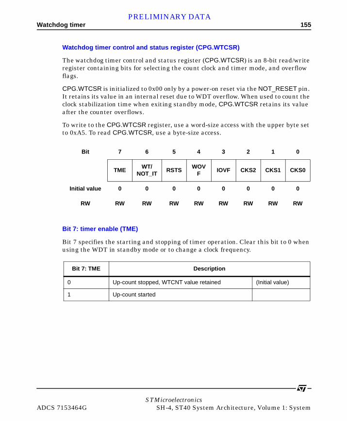
Watchdog timer 155PRELIMINARY DATA
Watchdog timer control and status register (CPG.WTCSR)
The watchdog timer control and status register (CPG.WTCSR) is an 8-bit read/write register containing bits for selecting the count clock and timer mode, and overflow flags.
CPG.WTCSR is initialized to 0x00 only by a power-on reset via the NOT_RESET pin. It retains its value in an internal reset due to WDT overflow. When used to count the clock stabilization time when exiting standby mode, CPG.WTCSR retains its value after the counter overflows.
To write to the CPG.WTCSR register, use a word-size access with the upper byte set to 0xA5. To read CPG.WTCSR, use a byte-size access.
Bit 7: timer enable (TME)
Bit 7 specifies the starting and stopping of timer operation. Clear this bit to 0 when using the WDT in standby mode or to change a clock frequency.
Bit 7 6 5 4 3 2 1 0
TMEWT/
NOT_ITRSTS
WOVF
IOVF CKS2 CKS1 CKS0
Initial value 0 0 0 0 0 0 0 0
RW RW RW RW RW RW RW RW RW
Bit 7: TME Description
0 Up-count stopped, WTCNT value retained (Initial value)
1 Up-count started
STMicroelectronicsADCS 7153464G SH-4, ST40 System Architecture, Volume 1: System
156 Watchdog timerPRELIMINARY DATA
Bit 6: timer mode select (WT/NOT_IT)
Bit 6 specifies whether the WDT is used as a watchdog timer or interval timer.
Note: the up-count may not be performed correctly if WT/NOT_IT is modified while the WDT is running.
Bit 5: reset select (RSTS)
Bit 5 specifies the kind of reset to be performed when CPG.WTCNT overflows in watchdog timer mode. This setting is ignored in interval timer mode.
Bit 4: watchdog timer overflow flag (WOVF)
Bit 4 indicates that CPG.WTCNT has overflowed in watchdog timer mode. This flag is not set in interval timer mode.
Bit 6: WT/NOT_IT Description
0 Interval timer mode (Initial value)
1 Watchdog timer mode
Bit 5: RSTS Description
0 Power-on reset (Initial value)
1 Manual reset
Bit 4: WOVF Description
0 No overflow (Initial value)
1 CPG.WTCNT has overflowed in watchdog timer mode
STMicroelectronicsSH-4, ST40 System Architecture, Volume 1: System ADCS 7153464G

Watchdog timer 157PRELIMINARY DATA
Bit 3: interval timer overflow flag (IOVF)
Bit 3 indicates that CPG.WTCNT has overflowed in interval timer mode. This flag is not set in watchdog timer mode.
Bits 2 to 0: clock select 2 to 0 (CKS2 to CKS0)
These bits select the clock used for the CPG.WTCNT count from eight clocks obtained by dividing the frequency divider two input clock. The overflow periods shown in the following table are based on a 150 MHz X1 output from the main clock divider. The up-count may not be performed correctly if bits CKS2 to CKS0 are modified while the WDT is running. Always stop the WDT before modifying these bits.
Bit 3: IOVF Description
0 No overflow (Initial value)
1 CPG.WTCNT has overflowed in interval timer mode
Bit 2: CKS2 Bit 1: CKS1 Bit 0: CKS0Description
Clock division ratio Overflow period
0 0 0 1/32 55 µs
1 1/64 109 µs
1 0 1/128 219 µs
1 1/256 437 µs
1 0 0 1/512 874 µs
1 1/1024 1.75 ms
1 0 1/2048 3.5 ms
1 1/4096 6.99 ms
STMicroelectronicsADCS 7153464G SH-4, ST40 System Architecture, Volume 1: System

158 Watchdog timerPRELIMINARY DATA
Writing to CPG.WTCNT and CPG.WTCSR
The watchdog timer counter (CPG.WTCNT) and watchdog timer control and status register (CPG.WTCSR) differ from other registers in being more difficult to write to. These registers must be written to with a word transfer instruction. They cannot be written to with a byte or longword transfer instruction.
When writing to CPG.WTCNT, perform the transfer with the upper byte set to 0x5A and the lower byte containing the write data.
When writing to CPG.WTCSR, perform the transfer with the upper byte set to 0xA5 and the lower byte containing the write data.
This transfer procedure writes the lower byte data to CPG.WTCNT or CPG.WTCSR.
The write formats are shown in Figure 19.
Figure 19: Writing to WTCNT and WTCSR
15 8 7 0
H'5A Write dataAddress: H'FFC00008 (H'1FC00008)
15 8 7 0
H'A5 Write dataAddress: H'FFC0000C (H'1FC0000C)
WTCSR write
WTCNT write
STMicroelectronicsSH-4, ST40 System Architecture, Volume 1: System ADCS 7153464G
Watchdog timer 159PRELIMINARY DATA
6.4.4 Using the WDT
Standby clearing procedure
The WDT is used when clearing standby mode by means of an NMI or other interrupt. The procedure is shown below. As the WDT does not operate when standby mode is cleared with a reset, the NOT_RESET pin should be held low until the clock stabilizes.
1 Be sure to set the TME bit in the CPG.WTCSR register to 0 before making a transition to standby mode. If the TME bit is set to 1, an inadvertent reset or interval timer interrupt may be caused when the count overflows.
2 Select the count clock to be used with bits CKS2 to CKS0 in the CPG.WTCSR register, and set the initial value in the CPG.WTCNT counter. Make these settings so that the time until the count overflows is at least as long as the clock oscillation stabilization time.
3 Make a transition to standby mode, and stop the clock, by executing a SLEEP instruction.
4 The WDT starts counting on detection of an NMI signal transition edge or an interrupt.
5 When the WDT count overflows, the CPG starts clock supply and the processor resumes operation. The WOVF flag in the CPG.WTCSR register is not set at this time.
6 The counter stops at a value of 0x000x01. The value at which the counter stops depends on the clock ratio.
Frequency changing procedure
The WDT is used in a frequency change using the PLL. It is not used when the frequency is changed simply by making a frequency divider switch.
1 Be sure to set the TME bit in the CPG.WTCSR register to 0 before making a frequency change. If the TME bit is set to 1, an inadvertent reset or interval timer interrupt may be caused when the count overflows.
2 Select the count clock to be used with bits CKS2 to CKS0 in the CPG.WTCSR register, and set the initial value in the CPG.WTCNT counter. Make these settings so that the time until the count overflows is at least as long as the clock oscillation stabilization time.
3 When the frequency control register (CPG.FRQCR) is modified, the clock stops, and the standby state is entered temporarily. The WDT starts counting.
STMicroelectronicsADCS 7153464G SH-4, ST40 System Architecture, Volume 1: System
160 Watchdog timerPRELIMINARY DATA
4 When the WDT count overflows, the CPG starts clock supply and the processor resumes operation. The WOVF flag in the CPG.WTCSR register is not set at this time.
5 The counter stops at a value of 0x00-0x01. The value at which the counter stops depends on the clock ratio.
Using watchdog timer mode
1 Set the WT/NOT_IT bit in the CPG.WTCSR register to 1, select the type of reset with the RSTS bit, and the count clock with bits CKS2-CKS0, and set the initial value in the CPG.WTCNT counter.
2 When the TME bit in the CPG.WTCSR register is set to 1, the count starts in watchdog timer mode.
3 During operation in watchdog timer mode, write 0x00 to the counter periodically so that it does not overflow.
4 When the counter overflows, the WDT sets the WOVF flag in the CPG.WTCSR register to 1, and generates a reset of the type specified by the RSTS bit. The counter then continues counting.
Using interval timer mode
When the WDT is operating in interval timer mode, an interval timer interrupt is generated each time the counter overflows. This enables interrupts to be generated at fixed intervals.
1 Set the WT/NOT_IT bit in the CPG.WTCSR register to 0. Select the count clock with bits CKS2 to CKS0, and set the initial value in the CPG.WTCNT counter.
2 When the TME bit in the CPG.WTCSR register is set to 1, the count starts in interval timer mode.
3 When the counter overflows, the WDT sets the IOVF flag in the CPG.WTCSR register to 1, and sends an interval timer interrupt request to INTC. The counter continues counting.
STMicroelectronicsSH-4, ST40 System Architecture, Volume 1: System ADCS 7153464G

Power management unit (PMU) 161PRELIMINARY DATA
6.5 Power management unit (PMU)The power management unit is responsible for controlling clock shutdown and startup for each of the on-chip modules. The power states are organized into a number of power down modes, each of which specify which modules are operating and which are halted. There are two sets of registers in the power management
unit. The CPG bank registers STBCR and STBCR2 control the power down modes and also the individual power-down state of legacy SH peripherals. The CLOCKGEN bank registers controls the power-down state of the ST40RA peripherals (PCI, DMAC, LMI and FMI).
Figure 20: Power management module function
PMU
STBCR
STBCR2
STATUS0
STATUS1
Clock domains (From CPG/CLOCKGEN)
... Module 1 Module 2 Module 3 Module n
STBREQCR
STBACKCR
CPG CLOCKGEN
STMicroelectronicsADCS 7153464G SH-4, ST40 System Architecture, Volume 1: System
162 Power management unit (PMU)PRELIMINARY DATA
6.5.1 Types of power-down modes
The following power-down modes and functions are provided:
• sleep mode,
• deep sleep mode,
• standby mode,
• module standby function (for individual power-down of on-chip peripheral modules).
Table 81 shows the conditions for entering these modes from the program execution state, the status of the CPU and peripheral modules in each mode, and the method of exiting each mode.
Powerdown mode
Entering conditions
Status
Exiting method
CPG CPUOn-chip
memory
On-chip peripheral modules
PinsExternal memory
Sleep SLEEP instruction executed while STBY bit is 0 in STBCR
Operating Halted (registers held)
Held Operating Held Refresh-ing
Interrupt
Reset
Deep sleep
DMAC module is put into standby Followed by the memory interface(s) being put into standby. Then the SLEEP instruction is executed while STBY bit is 0 in STBCR.
Operating Halted (registers held)
Held Operating (DMA halted)
Held Self- refresh-ing
Interrupt
Reset
Table 81: Status of CPU and peripheral modules in power-down modes
STMicroelectronicsSH-4, ST40 System Architecture, Volume 1: System ADCS 7153464G

Power management unit (PMU) 163PRELIMINARY DATA
Note: The RTC operates when the START bit in RTC.RCR2 is 1 (see chapter about Real-time clock).
SLEEP instruction is executed while STBY bit is 0 in STBCR.
Stand-by
SLEEP instruction executed while STBY bit is 1 in STBCR
Halted Halted (registers held)
Held Halted* Held All external memory Self- refresh-ing
Interrupt
Reset
Module standby
Setting MSTP bit to 1 in STBCR
or setting a bit in the STBREQCR.
Operating Operating Held Specified modules halted*
Held Refresh-ing
Clearing MSTP
bit/STBREQCR bit to 0
Reset
Powerdown mode
Entering conditions
Status
Exiting method
CPG CPUOn-chip
memory
On-chip peripheral modules
PinsExternal memory
Table 81: Status of CPU and peripheral modules in power-down modes
STMicroelectronicsADCS 7153464G SH-4, ST40 System Architecture, Volume 1: System

164 Power management unit (PMU)PRELIMINARY DATA
6.5.2 Register configuration
Table 82 and Table 83 show the registers used for power-down mode control.
DescriptionRegister
nameType
Initial value
CPG offsetAccess
size
Standby control register CPG.STBCR RW 0x00 0x04 8
Standby control register 2
CPG.STBCR2
RW 0x00 0x10 8
Table 82: CPG bank power down registers
Description Register name TypeInitial value
CLOCKGEN offset
Access size
Standby module request CLOCKGEN.STBREQCR RW 0x00 0x18 32
Set Standby module req CLOCKGEN.STBREQCR_SET WO - 0x20 32
Clear Standby module req
CLOCKGEN.STBREQCR_CLR WO - 0x28 32
Standby module acknowledge
CLOCKGEN.STBACKCR RO 0x00 0x30 32
Table 83: CLOCKGEN bank power-down registers
STMicroelectronicsSH-4, ST40 System Architecture, Volume 1: System ADCS 7153464G
Power management unit (PMU) 165PRELIMINARY DATA
6.5.3 Pin configuration
Table 84 shows the pins used for power-down mode control.
6.5.4 Register descriptions
Standby control register1 (CPG.STBCR)
The standby control register (CPG.STBCR) is an 8-bit read/write register that specifies the power- down mode status. It is initialized to 0x00 by a power- on reset via the NOT_RESET pin or due to watchdog timer overflow.
Pin Name Abbreviation I/O Function
Processor status 1
Processor status 0
STATUS1
STATUS0
Output Indicate the processors operating
statusA
HH: ResetHL: Sleep modeLH: Standby modeLL: Normal operation
A. H: high levelL: low level
Table 84: Power-down mode pins
1. Please Check the product datasheet to determine which STBCR bits are implemented for your device.
Bit 7 6 5 4 3 2 1 0
STBY PHZ PPU MSTP4 MSTP3 MSTP2 MSTP1 MSTP0
Initial value 0 0 0 0 0 0 0 0
RW RW RW RW RW RW RW RW RW
STMicroelectronicsADCS 7153464G SH-4, ST40 System Architecture, Volume 1: System
166 Power management unit (PMU)PRELIMINARY DATA
Bit 7: standby (STBY)
Bit 7 specifies a transition to standby mode.
Bit 6: peripheral module pin high impedance control (PHZ)
Bit 6 controls the state of peripheral module related pins in standby mode. When the PHZ bit is set to 1, peripheral module related pins go to the high-impedance state in standby mode.
For the relevant pins, see, Section 6.5.3: Pin configuration on page 165.
Bit 5: peripheral module pin pull-up control (PPU)
Bit 5 controls the state of peripheral module related pins. When the PPU bit is cleared to 0, the pull-up resistor is turned on for peripheral module related pins in the input or high-impedance state.
For the relevant pins, see Section : Peripheral module pin pull-up control on page 168.
Bit 4: unused
This bit has no functional use.
Bit 7: STBY Description
0 Transition to sleep mode on execution of SLEEP instruction (Initial value)
1 Transition to standby mode on execution of SLEEP instruction
Bit 6: PHZ Description
0 Peripheral module related pins are in normal state (Initial value)
1 Peripheral module related pins go to high-impedance state
Bit 5: PPU Description
0 Peripheral module related pin pull-up resistors are on (Initial value)
1 Peripheral module related pin pull-up resistors are off
STMicroelectronicsSH-4, ST40 System Architecture, Volume 1: System ADCS 7153464G

Power management unit (PMU) 167PRELIMINARY DATA
Bit 3: module stop 3 (MSTP3)
Bit 3 specifies stopping of the clock supply to serial communication interface channel 2 (SCIF2) among the on-chip peripheral modules. The clock supply to the SCIF2 is stopped when the MSTP3 bit is set to 1.
Bit 2: module stop 2 (MSTP2)
Bit 2 specifies stopping of the clock supply to the timer unit (TMU) among the on-chip peripheral modules. The clock supply to the TMU is stopped when the MSTP2 bit is set to 1.
Bit 1: module stop 1 (MSTP1)
Bit 1 specifies stopping of the clock supply to the realtime clock (RTC) among the on- chip peripheral modules. The clock supply to the RTC is stopped when the MSTP1 bit is set to 1. When the clock supply is stopped, RTC registers cannot be accessed but the counters continue to operate.
Bit 3: MSTP3
Description
0 SCIF2 operates (Initial value)
1 SCIF2 clock supply is stopped
Bit 2: MSTP2
Description
0 TMU operates (Initial value)
1 TMU clock supply is stopped
Bit 1: MSTP1
Description
0 RTC operates (Initial value)
1 RTC clock supply is stopped
STMicroelectronicsADCS 7153464G SH-4, ST40 System Architecture, Volume 1: System
168 Power management unit (PMU)PRELIMINARY DATA
Bit 0: module stop 0 (MSTP0)
Bit 0 specifies stopping of the clock supply to serial communication interface channel 1 (SCIF1) among the on-chip peripheral modules. The clock supply to SCIF1 is stopped when the MSTP0 bit is set to 1.
Peripheral module pin pull-up control
When bit 5 in the standby control register (CPG.STBCR) is set to 0, peripheral module related pins are pulled up when in the input or high-impedance state.
Bit 0: MSTP0
Description
0 SCIF1 operates (Initial value)
1 SCIF1 clock supply is stopped
SCIF1 related pins MD0/SCK MD1/TXD2 MD2/RXD2
MD7/TXD MD8/RTS2 SCK2/NOT_MRESET
RXD CTS2
DMA related pins NOT_DREQ0 DACK0 DRAK0
NOT_DREQ1 DACK1 DRAK1
TMU related pin TCLK
Table 85: Relevant pins
STMicroelectronicsSH-4, ST40 System Architecture, Volume 1: System ADCS 7153464G

Power management unit (PMU) 169PRELIMINARY DATA
Standby control register 2 1(CPG.STBCR2)
Standby control register 2 (CPG.STBCR2) is an 8-bit read/write register that specifies additional standby behavior. It is initialized to 0x00 by a power-on reset via the NOT_RESET pin or due to watchdog timer overflow.
Bit 7: unused
Bit 6: status pin high-impedance control (STHZ)
This bit selects whether the STATUS0 and STATUS1 pins are set to high-impedance when in hardware standby mode.
Bits 5 to 2: reserved
Only zero should only be written to these bits; operation cannot be guaranteed if one is written. These bits are always read as zero.
1. Please check the datasheet to determine which bits are implemented for your device
Bit 7 6 5 4 3 2 1 0
- STHZ - - - - MSTP6 MSTP5
Initial value 0 0 0 0 0 0 0 0
RW RW RW R R R R RW RW
Bit 6: STHZ Description
0 Sets STATUS0/1 Pins to high Impedance when in hardware standby mode
(Initial value)
1 Drives STATUS0/1 Pins to LH when in hardware standby mode.
STMicroelectronicsADCS 7153464G SH-4, ST40 System Architecture, Volume 1: System
170 Power management unit (PMU)PRELIMINARY DATA
Bit 1: module stop 6 (MSTP6)
Bit 1 specifies that the clock supply to the store queue (SQ) in the cache controller (CCN) is stopped. Setting the MSTP6 bit to 1 stops the clock supply to the SQ, and the SQ functions are therefore unavailable.
Bit 0: module stop 5 (MSTP5)
Specifies that. of the internal modules, the clock supply to the user break controller (UBC) is stopped.
Standby control request register (CLOCKGEN.STBREQCR)
Standby control may be effected by the use of the STBREQCR (standby request) and STBACK (standby acknowledge) registers. These registers implement the power down protocol for ST modules. Each bit of these registers corresponds to an SuperHyway module. A module may be requested to be powered down by writing a 1 to the appropriate bit in the STBREQCR register. When that module has completed its power down sequence, and the clock to it has been stopped, the corresponding bit in the STBACKCR is set. This procedure allows precise software control of putting modules into standby.
To enable independent setting and clearing of the STBREQCR bits two auxiliary pseudo registers are provided. The STBREQCR_SET pseudo register allows STBREQCR bits to be set independently. Writing 1 in STBREQCR_SET sets the corresponding bit in STBREQCR, a 0 leaves the bit unchanged. The STBREQCR_CLR pseudo register allows bits to be cleared individually. Writing a 1 in STBREQCR_CLR resets the corresponding bit in STBREQCR, a 0 leaves the bit unchanged. See the product datasheet for details of these registers.
Bit 1: MSTP6 Description
0 SQ operating (Initial value)
1 Clock supply to SQ is stopped
Bit 0: MSTP5 Description
0 UBCoperating (Initial value)
1 Clock supply to UBC is stopped
STMicroelectronicsSH-4, ST40 System Architecture, Volume 1: System ADCS 7153464G

Functionality 171PRELIMINARY DATA
Standby control acknowledge register (CLOCKGEN.STBACKCR)
See the datasheet for details of this register.
6.6 Functionality
6.6.1 Sleep mode
Transition to sleep mode
If a SLEEP instruction is executed when the STBY bit in CPG.STBCR is cleared to 0, the chip switches from the program execution state to sleep mode. After execution of the SLEEP instruction, the CPU halts but its register contents are retained. The on-chip peripheral modules continue to operate, and the clock continues to be output from the CLKOUT pin.
In sleep mode, a high-level signal is output at the STATUS1 pin, and a low-level signal at the STATUS0 pin.
Exit from sleep mode
Sleep mode is exited by means of an interrupt (NMI, IRL, or on-chip peripheral module) or a reset. In sleep mode, interrupts are accepted even if the BL bit in the SR register is 1. If necessary, SPC and SSR should be saved to the stack before executing the SLEEP instruction.
Exit by interrupt
When an NMI, IRL, or on-chip peripheral module interrupt is generated, sleep mode is exited and interrupt exception handling is executed. The code corresponding to the interrupt source is set in the INTEVT register.
Exit by reset
Sleep mode is exited by means of a power-on or manual reset via the NOT_RESET pin, or a power-on or manual reset executed when the watchdog timer overflows.
STMicroelectronicsADCS 7153464G SH-4, ST40 System Architecture, Volume 1: System
172 FunctionalityPRELIMINARY DATA
6.6.2 Deep sleep mode
Deep sleep mode is similar to sleep mode except that additionally DMAC and the memory interfaces are in a low power state.
Transition to deep sleep mode
To enter deep sleep mode first power down the DMAC then power down the memory interfaces. This is accomplished using the module standby procedure described in Section 6.7.2. Then if a SLEEP instruction is executed when the STBY bit in CPG.STBCR is cleared to 0 the chip switches from the program execution state to deep sleep mode. After execution of the SLEEP instruction, the CPU halts but its register contents are retained.
Except for the powered down modules, on-chip peripheral modules continue to operate, and the clock continues to be output from the CLKOUT pin.
In deep sleep mode, a high-level signal is output at the STATUS1 pin, and a low-level signal at the STATUS0 pin.
Exit from deep sleep mode
As with sleep mode, deep sleep mode is exited by means of an interrupt (NMI, IRL, or on-chip peripheral module or a reset. Software can then power up the modules which were powered down when deep sleep was entered. See Section 6.7.4 for the procedure for powering up these modules.
6.6.3 Standby mode
Transition to standby mode
If a SLEEP instruction is executed when the STBY bit in CPG.STBCR is set to 1, the chip switches from the program execution state to standby mode. In standby mode, the on-chip peripheral modules halt as well as the CPU. Clock output from the CLKOUT pin is also stopped.
The CPU and cache register contents are retained. Some on-chip peripheral module registers are initialized. The state of the peripheral module registers in standby mode is shown in Table 86.
STMicroelectronicsSH-4, ST40 System Architecture, Volume 1: System ADCS 7153464G
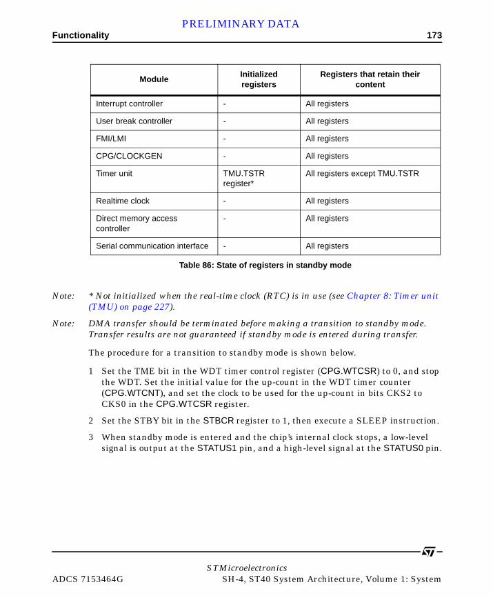
Functionality 173PRELIMINARY DATA
Note: * Not initialized when the real-time clock (RTC) is in use (see Chapter 8: Timer unit (TMU) on page 227).
Note: DMA transfer should be terminated before making a transition to standby mode. Transfer results are not guaranteed if standby mode is entered during transfer.
The procedure for a transition to standby mode is shown below.
1 Set the TME bit in the WDT timer control register (CPG.WTCSR) to 0, and stop the WDT. Set the initial value for the up-count in the WDT timer counter (CPG.WTCNT), and set the clock to be used for the up-count in bits CKS2 to CKS0 in the CPG.WTCSR register.
2 Set the STBY bit in the STBCR register to 1, then execute a SLEEP instruction.
3 When standby mode is entered and the chip’s internal clock stops, a low-level signal is output at the STATUS1 pin, and a high-level signal at the STATUS0 pin.
ModuleInitialized registers
Registers that retain their content
Interrupt controller - All registers
User break controller - All registers
FMI/LMI - All registers
CPG/CLOCKGEN - All registers
Timer unit TMU.TSTR register*
All registers except TMU.TSTR
Realtime clock - All registers
Direct memory access controller
- All registers
Serial communication interface - All registers
Table 86: State of registers in standby mode
STMicroelectronicsADCS 7153464G SH-4, ST40 System Architecture, Volume 1: System
174 FunctionalityPRELIMINARY DATA
Exit from standby mode
Standby mode is exited by means of an interrupt (NMI, IRL, or on-chip peripheral module or a reset via the NOT_RESET pin.
Exit by interrupt
A hot start can be performed by means of the on-chip WDT. When an NMI, IRL1, or on- chip peripheral module (except interval timer)2 interrupt is detected, the WDT starts counting. After the count overflows, clocks are supplied to the entire chip, standby mode is exited, and the STATUS1 and STATUS0 pins both go low. Interrupt exception handling is then executed, and the code corresponding to the interrupt source is set in the INTEVT register. In standby mode, interrupts are accepted even if the BL bit in the SR register is 1, and so, if necessary, SPC and SSR should be saved to the stack before executing the SLEEP instruction.
The phase of the CLKOUT pin clock output may be unstable immediately after an interrupt is detected, until standby mode is exited.
Exit by reset
Standby mode is exited by means of a reset (power-on manual) via the NOT_RESET pin. The NOT_RESET pin should be held low until clock oscillation stabilizes. The internal clock continues to be output at the CLKOUT pin.
6.6.4 Clock pause function
In standby mode, it is possible to stop or change the frequency of the clock input from the EXTAL pin. This function is used as follows.
1 Enter standby mode following the transition procedure described above.
2 When standby mode is entered and the chip’s internal clock stops, a low-level signal is output at the STATUS1 pin, and a high-level signal at the STATUS0 pin.
3 The input clock is stopped, or its frequency changed, after the STATUS1 pin goes low and the STATUS0 pin high.
1. Only when the RTC clock (32.768 kHz) is operating (see Chapter 3: Interrupt controller (INTC) on page 15), standby mode can be exited by means of IRL3–IRL0 (when the IRL3–IRL0 level is higher than the SR register I3–I0 mask level).
2. Standby mode can be exited by means of an RTC interrupt.
STMicroelectronicsSH-4, ST40 System Architecture, Volume 1: System ADCS 7153464G
Module standby function 175PRELIMINARY DATA
4 When the frequency is changed, input an NMI or IRL interrupt after the change. When the clock is stopped, input an NMI or IRL interrupt after applying the clock.
5 After the time set in the WDT, clock supply begins inside the chip, the STATUS1 and STATUS0 pins both go low, and operation is resumed from interrupt exception handling.
6.7 Module standby function
6.7.1 Transition to module standby function(CPG modules)
Setting the MSTP4 to MSTP0 bits in the standby control register to 1 enables the clock supply to the corresponding on-chip peripheral modules to be halted. Use of this function allows power consumption in sleep mode to be further reduced.
In the module standby state, the on-chip peripheral module external pins retain their states prior to halting of the modules, and most registers retain their states prior to halting of the modules.
Bit Description
MSTP3 0 SCIF2 operates
1 Clock supplied to SCIF2 is stopped
MSTP2 0 TMU operates
1 Clock supplied to TMU is stopped, and register is initialized*1
MSTP1 0 RTC operates
1 Clock supplied to RTC is stopped*2
MSTP0 0 SCIF1 operates
1 Clock supplied to SCIF1 is stopped
STMicroelectronicsADCS 7153464G SH-4, ST40 System Architecture, Volume 1: System

176 Module standby functionPRELIMINARY DATA
Note: 1. The register initialized is the same as in standby mode, but initialization is not performed if the RTC clock is not in use (see Chapter 8: Timer unit (TMU) on page 227.
2. The counter operates when the START bit in RCR2 is 1 (see Chapter 7: Real-time clock (RTC) on page 179.
6.7.2 Transition to module standby function (CLOCKGEN modules)
The modules controlled by the CLOCKGEN register bank use a different method for entering and exiting the power down state from those controlled by the CPG register bank. The CLOCKGEN controlled modules employ a software handshake mechanism which allows software to control the order in which the clock used by each module is started and stopped.
The FMI, LMI, DMAC and PCI modules can be stopped (that is powered down) by setting the appropriate bit of the CLOCKGEN.STBREQCR register. Sometime later the hardware will set the corresponding bit in the CLOCKGEN.STBACKCR to 1 indicating that the clock to the module has been stopped. The time delay between these events depends on the particular module being requested to stop and its state at the time of the request. Software should normally stop modules one by one, checking that a module has stopped before requesting that the next module is stopped taking care to avoid any potential deadlock condition.
6.7.3 Exit from module standby function(CPG modules)
The module standby function is exited by setting the MSTP4 to MSTP0 bits to 0, or by a power-on reset via the NOT_RESET pin or a power-on reset caused by watchdog timer overflow.
STMicroelectronicsSH-4, ST40 System Architecture, Volume 1: System ADCS 7153464G

STATUS pin change timing 177PRELIMINARY DATA
6.7.4 Exit from module standby function(CLOCKGEN modules)
The FMI, LMI, DMAC and PCI modules can be started (that is powered up) by writing a 0 into the appropriate field of the CLOCKGEN.STBREQCR. Sometime later the hardware will set the corresponding bit in the CLOCKGEN.STBACKCR to 0 indicating that the clock to the module has been re-started. The time delay between these events depends on the particular module being requested to start and its state at the time it was stopped. Software should normally start modules one by one, checking that a module has started before requesting the next module is started.
6.8 STATUS pin change timing The STATUS1 and STATUS0 pin change timing is shown below.
The meaning of the STATUS pin settings is as follows:
The meaning of the clock units is as follows:
• Bcyc: Bus clock cycle,
• Pcyc: Peripheral clock cycle.
Pin setting Meaning STATUS1 pin STATUS0 pin
HH Reset High High
HL Sleep High Low
LH Standby Low High
LL Normal Low Low
Table 87: STATUS pin settings
STMicroelectronicsADCS 7153464G SH-4, ST40 System Architecture, Volume 1: System
178 STATUS pin change timingPRELIMINARY DATA
STMicroelectronicsSH-4, ST40 System Architecture, Volume 1: System ADCS 7153464G
PRELIMINARY DATA
STMicroelectroniADCS 7153464G SH-4, ST40 S
7
Real-time clock (RTC) 7.1 OverviewThe system includes an on-chip real-time clock (RTC) and a 32.768 kHz crystal oscillator for use by the RTC.
7.1.1 Features
The RTC has the following features:
• clock and calendar functions (BCD display), counts:
- seconds,
- minutes,
- hours,
- day of the week,
- days,
- months,
- years,
• 1 to 64 Hz timer (binary display),
- the 64 Hz counter register indicates a state of 64 Hz to 1 Hz within the RTC frequency divider,
• start and stop functions,
• 30 second adjustment function,
csystem Architecture, Volume 1: System
180 OverviewPRELIMINARY DATA
• alarm interrupts,
- comparison with second, minute, hour, day-of-week, day, or month can be selected as the alarm interrupt condition,
• periodic interrupts,
- an interrupt period of 1/256 second, 1/64 second, 1/16 second, 1/4 second, 1/2 second, 1 second, or 2 seconds can be selected,
• carry interrupt,
- carry interrupt function indicating a second counter carry, or a 64 Hz counter carry when the 64 Hz counter is read,
• automatic leap year adjustment.
STMicroelectronicsSH-4, ST40 System Architecture, Volume 1: System ADCS 7153464G
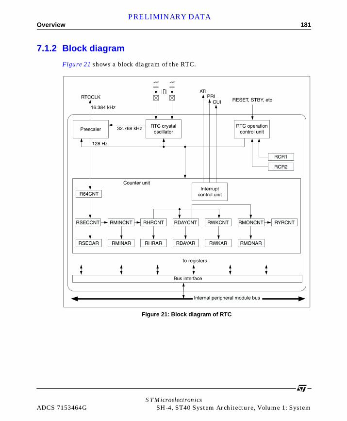
Overview 181PRELIMINARY DATA
7.1.2 Block diagram
Figure 21 shows a block diagram of the RTC.
Figure 21: Block diagram of RTC
R64CNT
RTCCLK
16.384 kHz
32.768 kHz
128 Hz
ATIPRI
CUI
RCR1
RCR2
RYRCNTRMONCNTRWKCNTRDAYCNTRHRCNTRMINCNTRSECCNT
RSECAR RMINAR RHRAR RDAYAR RWKAR RMONAR
PrescalerRTC crystal
oscillatorRTC operation
control unit
RESET, STBY, etc
Counter unitInterrupt
control unit
To registers
Bus interface
Internal peripheral module bus
STMicroelectronicsADCS 7153464G SH-4, ST40 System Architecture, Volume 1: System
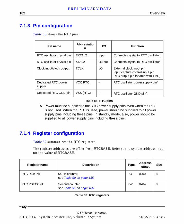
182 OverviewPRELIMINARY DATA
7.1.3 Pin configuration
Table 88 shows the RTC pins.
7.1.4 Register configuration
Table 89 summarizes the RTC registers.
The register addresses are offset from RTCBASE. Refer to the system address map for the value of RTCBASE.
Pin nameAbbreviatio
nI/O Function
RTC oscillator crystal pin EXTAL2 Input Connects crystal to RTC oscillator
RTC oscillator crystal pin XTAL2 Output Connects crystal to RTC oscillator
Clock input/clock output TCLK I/O External clock input pinInput capture control input pinRTC output pin (shared with TMU)
Dedicated RTC power supply
VCC RTC - RTC oscillator power supply pin*
Dedicated RTC GND pin VSS (RTC) - RTC oscillator GND pinA
A. Power must be supplied to the RTC power supply pins even when the RTC is not used. When the RTC is used, power should be supplied to all power supply pins including these pins. In standby mode, also, power should be supplied to all power supply pins including these pins.
Table 88: RTC pins
Register name Description TypeAddress
offsetSize
RTC.R64CNT 64 Hz counter, see Table 90 on page 185
RO 0x00 8
RTC.RSECCNT Second counter, see Table 91 on page 186
RW 0x04 8
Table 89: RTC registers
STMicroelectronicsSH-4, ST40 System Architecture, Volume 1: System ADCS 7153464G

Overview 183PRELIMINARY DATA
RTC.RMINCNT Minute counter, see Table 92 on page 188
RW 0x08 8
RTC.RHRCNT Hour counter, see Table 93 on page 190
RW 0x0C 8
RTC.RWKCNT Day of week counter, see Table 94 on page 192
RW 0x10 8
RTC.RDAYCNT Day counter, see Table 95 on page 194
RW 0x14 8
RTC.RMONCNT Month counter, see Table 96 on page 196
RW 0x18 8
RTC.RYRCNT Year counter, see Table 97 on page 198
RW 0x1C 16
RTC.RSECAR Second alarm register, see Table 98 on page 200
RW 0x20 8
RTC.RMINAR Minute alarm register, see Table 99 on page 202
RW 0x24 8
RTC.RHRAR Hour alarm register, see Table 100 on page 204
RW 0x28 8
RTC.RWKAR Day of week alarm register, see Table 101 on page 206
RW 0x2C 8
RTC.RDAYAR Day alarm register, see Table 102 on page 208
RW 0x30 8
RTC.RMONAR Month alarm register, see Table 103 on page 210
RW 0x34 8
RTC.RCR1 RTC control register 1, see Table 104 on page 212
RW 0x38 8
Register name Description TypeAddress
offsetSize
Table 89: RTC registers
STMicroelectronicsADCS 7153464G SH-4, ST40 System Architecture, Volume 1: System

184 OverviewPRELIMINARY DATA
7.1.5 Register initialization
Register name Power-on reset Manual reset Standby mode Initial value
RTC.R64CNT Counts Counts Counts Undefined
RTC.RSECCNT Counts Counts Counts Undefined
RTC.RMINCNT Counts Counts Counts Undefined
RTC.RHRCNT Counts Counts Counts Undefined
RTC.RWKCNT Counts Counts Counts Undefined
RTC.RDAYCNT Counts Counts Counts Undefined
RTC.RMONCNT Counts Counts Counts Undefined
RTC.RYRCNT Counts Counts Counts Undefined
RTC.RSECAR InitializedA
A. The ENB bit in each register is initialized.
Held Held UndefinedA
RTC.RMINAR InitializedA Held Held UndefinedA
RTC.RHRAR InitializedA Held Held UndefinedA
RTC.RWKAR InitializedA Held Held UndefinedA
RTC.RDAYAR InitializedA Held Held UndefinedA
RTC.RMONAR InitializedA Held Held UndefinedA
RTC.RCR1 Initialized Initialized Held 0x00B
B. The value of the CF bit and AF bit is undefined.
RTC.RCR2 Initialized InitializedC
C. Bits other than the RTCEN bit and START bit are initialized.
Held 0x09D
D. The value of the PEF bit is undefined.
RTC.R64CNT Counts Counts Counts Undefined
RTC.RSECCNT Counts Counts Counts Undefined
RTC.RMINCNT Counts Counts Counts Undefined
STMicroelectronicsSH-4, ST40 System Architecture, Volume 1: System ADCS 7153464G
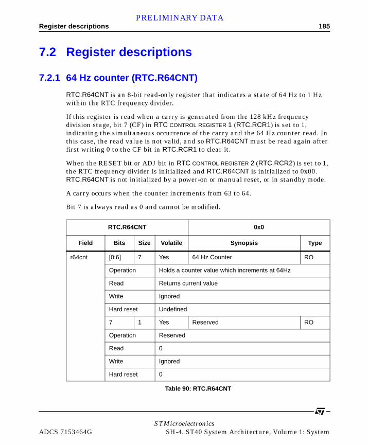
Register descriptions 185PRELIMINARY DATA
7.2 Register descriptions
7.2.1 64 Hz counter (RTC.R64CNT)
RTC.R64CNT is an 8-bit read-only register that indicates a state of 64 Hz to 1 Hz within the RTC frequency divider.
If this register is read when a carry is generated from the 128 kHz frequency division stage, bit 7 (CF) in RTC CONTROL REGISTER 1 (RTC.RCR1) is set to 1, indicating the simultaneous occurrence of the carry and the 64 Hz counter read. In this case, the read value is not valid, and so RTC.R64CNT must be read again after first writing 0 to the CF bit in RTC.RCR1 to clear it.
When the RESET bit or ADJ bit in RTC CONTROL REGISTER 2 (RTC.RCR2) is set to 1, the RTC frequency divider is initialized and RTC.R64CNT is initialized to 0x00. RTC.R64CNT is not initialized by a power-on or manual reset, or in standby mode.
A carry occurs when the counter increments from 63 to 64.
Bit 7 is always read as 0 and cannot be modified.
RTC.R64CNT 0x0
Field Bits Size Volatile Synopsis Type
r64cnt [0:6] 7 Yes 64 Hz Counter RO
Operation Holds a counter value which increments at 64Hz
Read Returns current value
Write Ignored
Hard reset Undefined
7 1 Yes Reserved RO
Operation Reserved
Read 0
Write Ignored
Hard reset 0
Table 90: RTC.R64CNT
STMicroelectronicsADCS 7153464G SH-4, ST40 System Architecture, Volume 1: System
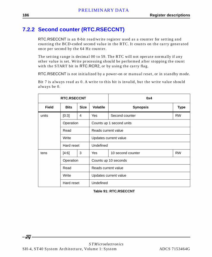
186 Register descriptionsPRELIMINARY DATA
7.2.2 Second counter (RTC.RSECCNT)
RTC.RSECCNT is an 8-bit read/write register used as a counter for setting and counting the BCD-coded second value in the RTC. It counts on the carry generated once per second by the 64 Hz counter.
The setting range is decimal 00 to 59. The RTC will not operate normally if any other value is set. Write processing should be performed after stopping the count with the START bit in RTC.RCR2, or by using the carry flag.
RTC.RSECCNT is not initialized by a power-on or manual reset, or in standby mode.
Bit 7 is always read as 0. A write to this bit is invalid, but the write value should always be 0.
RTC.RSECCNT 0x4
Field Bits Size Volatile Synopsis Type
units [0:3] 4 Yes Second counter RW
Operation Counts up 1 second units
Read Reads current value
Write Updates current value
Hard reset Undefined
tens [4:6] 3 Yes 10 second counter RW
Operation Counts up 10 seconds
Read Reads current value
Write Updates current value
Hard reset Undefined
Table 91: RTC.RSECCNT
STMicroelectronicsSH-4, ST40 System Architecture, Volume 1: System ADCS 7153464G

Register descriptions 187PRELIMINARY DATA
7 1 Yes Reserved RO
Operation Reserved
Read 0
Write Ignored
Hard reset 0
RTC.RSECCNT 0x4
Field Bits Size Volatile Synopsis Type
Table 91: RTC.RSECCNT
STMicroelectronicsADCS 7153464G SH-4, ST40 System Architecture, Volume 1: System
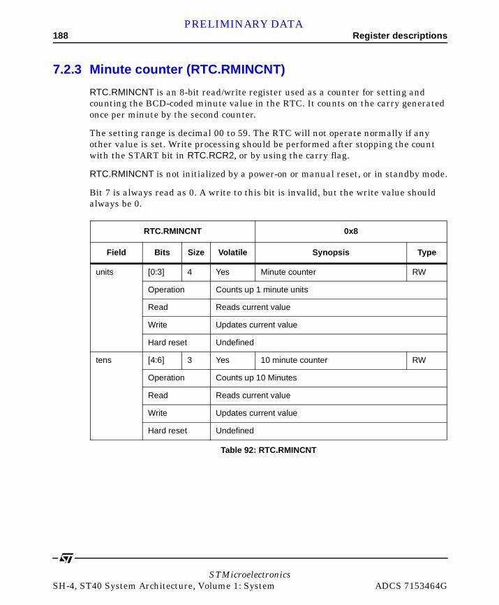
188 Register descriptionsPRELIMINARY DATA
7.2.3 Minute counter (RTC.RMINCNT)
RTC.RMINCNT is an 8-bit read/write register used as a counter for setting and counting the BCD-coded minute value in the RTC. It counts on the carry generated once per minute by the second counter.
The setting range is decimal 00 to 59. The RTC will not operate normally if any other value is set. Write processing should be performed after stopping the count with the START bit in RTC.RCR2, or by using the carry flag.
RTC.RMINCNT is not initialized by a power-on or manual reset, or in standby mode.
Bit 7 is always read as 0. A write to this bit is invalid, but the write value should always be 0.
RTC.RMINCNT 0x8
Field Bits Size Volatile Synopsis Type
units [0:3] 4 Yes Minute counter RW
Operation Counts up 1 minute units
Read Reads current value
Write Updates current value
Hard reset Undefined
tens [4:6] 3 Yes 10 minute counter RW
Operation Counts up 10 Minutes
Read Reads current value
Write Updates current value
Hard reset Undefined
Table 92: RTC.RMINCNT
STMicroelectronicsSH-4, ST40 System Architecture, Volume 1: System ADCS 7153464G

Register descriptions 189PRELIMINARY DATA
7 1 Yes Reserved RO
Operation Reserved
Read 0
Write Ignored
Hard reset 0
RTC.RMINCNT 0x8
Field Bits Size Volatile Synopsis Type
Table 92: RTC.RMINCNT
STMicroelectronicsADCS 7153464G SH-4, ST40 System Architecture, Volume 1: System
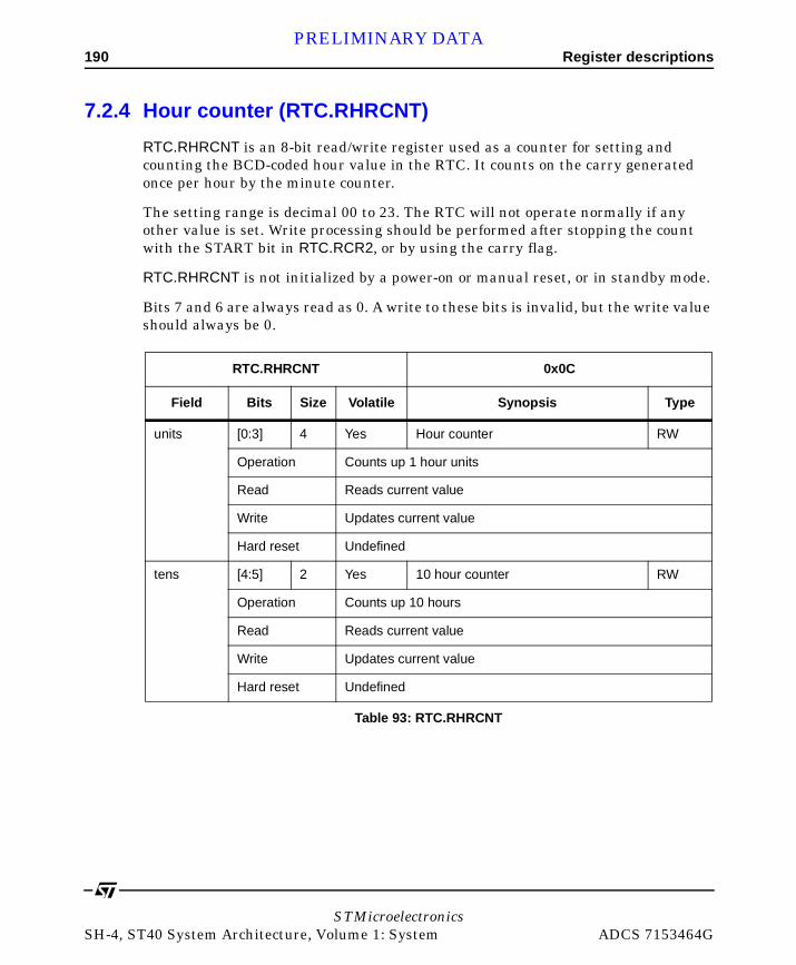
190 Register descriptionsPRELIMINARY DATA
7.2.4 Hour counter (RTC.RHRCNT)
RTC.RHRCNT is an 8-bit read/write register used as a counter for setting and counting the BCD-coded hour value in the RTC. It counts on the carry generated once per hour by the minute counter.
The setting range is decimal 00 to 23. The RTC will not operate normally if any other value is set. Write processing should be performed after stopping the count with the START bit in RTC.RCR2, or by using the carry flag.
RTC.RHRCNT is not initialized by a power-on or manual reset, or in standby mode.
Bits 7 and 6 are always read as 0. A write to these bits is invalid, but the write value should always be 0.
RTC.RHRCNT 0x0C
Field Bits Size Volatile Synopsis Type
units [0:3] 4 Yes Hour counter RW
Operation Counts up 1 hour units
Read Reads current value
Write Updates current value
Hard reset Undefined
tens [4:5] 2 Yes 10 hour counter RW
Operation Counts up 10 hours
Read Reads current value
Write Updates current value
Hard reset Undefined
Table 93: RTC.RHRCNT
STMicroelectronicsSH-4, ST40 System Architecture, Volume 1: System ADCS 7153464G
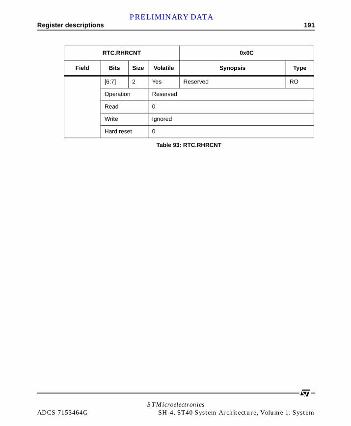
Register descriptions 191PRELIMINARY DATA
[6:7] 2 Yes Reserved RO
Operation Reserved
Read 0
Write Ignored
Hard reset 0
RTC.RHRCNT 0x0C
Field Bits Size Volatile Synopsis Type
Table 93: RTC.RHRCNT
STMicroelectronicsADCS 7153464G SH-4, ST40 System Architecture, Volume 1: System

192 Register descriptionsPRELIMINARY DATA
7.2.5 Day-of-week counter (RTC.RWKCNT)
RTC.RWKCNT is an 8-bit read/write register used as a counter for setting and counting the BCD-coded day-of- week value in the RTC. It counts on the carry generated once per day by the hour counter.
The setting range is decimal 0 to 6. The RTC will not operate normally if any other value is set. Write processing should be performed after stopping the count with the START bit in RTC.RCR2, or by using the carry flag.
RTC.RWKCNT is not initialized by a power-on or manual reset, or in standby mode.
Bits 7 to 3 are always read as 0. A write to these bits is invalid, but the write value should always be 0.
RTC.RWKCNT 0x10
Field Bits Size Volatile Synopsis Type
units [0:2] 3 Yes Day of week RW
Operation Indicates day of week
Read Returns day of week code:
0: Sunday
1: Monday
2: Tuesday
3: Wednesday
4: Thursday
5: Friday
6: Saturday
Write Updates current value
Hard reset Undefined
Table 94: RTC.RWKCNT
STMicroelectronicsSH-4, ST40 System Architecture, Volume 1: System ADCS 7153464G

Register descriptions 193PRELIMINARY DATA
[3:7] 5 Yes Reserved RO
Operation Reserved
Read 0
Write Ignored
Hard reset 0
RTC.RWKCNT 0x10
Field Bits Size Volatile Synopsis Type
Table 94: RTC.RWKCNT
STMicroelectronicsADCS 7153464G SH-4, ST40 System Architecture, Volume 1: System

194 Register descriptionsPRELIMINARY DATA
7.2.6 Day counter (RTC.RDAYCNT)
RTC.RDAYCNT is an 8-bit read/write register used as a counter for setting and counting the BCD-coded day value in the RTC. It counts on the carry generated once per day by the hour counter.
The setting range is decimal 01 to 31. The RTC will not operate normally if any other value is set. Write processing should be performed after stopping the count with the START bit in RTC.RCR2, or by using the carry flag. RTC.RDAYCNT is not initialized by a power-on or manual reset, or in standby mode.
The setting range for RTC.RDAYCNT depends on the month and whether the year is a leap year, so care is required when making the setting. Bits 7 and 6 are always read as 0. A write to these bits is invalid, but the write value should always be 0.
RTC.RDAYCNT 0x14
Field Bits Size Volatile Synopsis Type
units [0:3] 4 Yes Day counter RW
Operation Counts up 1 day units
Read Reads current value
Write Updates current value
Hard reset Undefined
tens [4:5] 2 Yes 10 day counter RW
Operation Counts up 10 days
Read Reads current value
Write Updates current value
Hard reset Undefined
Table 95: RTC.RDAYCNT
STMicroelectronicsSH-4, ST40 System Architecture, Volume 1: System ADCS 7153464G

Register descriptions 195PRELIMINARY DATA
[6:7] 2 Yes Reserved RO
Operation Reserved
Read 0
Write Ignored
Hard reset 0
RTC.RDAYCNT 0x14
Field Bits Size Volatile Synopsis Type
Table 95: RTC.RDAYCNT
STMicroelectronicsADCS 7153464G SH-4, ST40 System Architecture, Volume 1: System

196 Register descriptionsPRELIMINARY DATA
7.2.7 Month counter (RTC.RMONCNT)
RTC.RMONCNT is an 8-bit read/write register used as a counter for setting and counting the BCD-coded month value in the RTC. It counts on the carry generated once per month by the day counter.
The setting range is decimal 01 to 12. The RTC will not operate normally if any other value is set. Write processing should be performed after stopping the count with the START bit in RTC.RCR2, or by using the carry flag.
RTC.RMONCNT is not initialized by a power-on or manual reset, or in standby mode.
Bits 7 to 5 are always read as 0. A write to these bits is invalid, but the write value should always be 0
RTC.RMONCNT 0x18
Field Bits Size Volatile Synopsis Type
units [0:3] 4 Yes Month counter RW
Operation Counts up 1 month units
Read Reads current value
Write Updates current value
Hard reset Undefined
tens 4 1 Yes 10 month Counter RW
Operation Counts up 10 Months
Read Reads current value
Write Updates current value
Only values 0 to 9 are defined.
Hard reset Undefined
Table 96: RTC.RMONCNT
STMicroelectronicsSH-4, ST40 System Architecture, Volume 1: System ADCS 7153464G

Register descriptions 197PRELIMINARY DATA
[5:7] 3 Yes Reserved RO
Operation Reserved
Read 0
Write Ignored
Hard reset 0
RTC.RMONCNT 0x18
Field Bits Size Volatile Synopsis Type
Table 96: RTC.RMONCNT
STMicroelectronicsADCS 7153464G SH-4, ST40 System Architecture, Volume 1: System

198 Register descriptionsPRELIMINARY DATA
7.2.8 Year counter (RTC.RYRCNT)
RTC.RYRCNT is a 16-bit read/write register used as a counter for setting and counting the BCD-coded year value in the RTC. It counts on the carry generated once per year by the month counter.
The setting range is decimal 0000 to 9999. The RTC will not operate normally if any other value is set. Write processing should be performed after stopping the count with the START bit in RTC.RCR2, or by using the carry flag.
RTC.RYRCNT is not initialized by a power-on or manual reset, or in standby mode.
RTC.RYRCNT 0x1C
Field Bits Size Volatile Synopsis Type
units [0:3] 4 Yes Year Counter RW
Operation Counts up 1 year units
Read Reads current value
Write Updates current value
Hard reset Undefined
tens [4:7] 4 Yes 10 year Counter RW
Operation Counts up 10 years
Read Reads current value
Write Updates current value
Only values 0 to 9 are defined.
Hard reset Undefined
Table 97: RTC.RYRCNT
STMicroelectronicsSH-4, ST40 System Architecture, Volume 1: System ADCS 7153464G
Register descriptions 199PRELIMINARY DATA
hundreds [8:11] 4 Yes 100 year Counter RW
Operation Counts up 100 years
Read Reads current value
Write Updates current value
Only values 0 to 9 are defined.
Hard reset Undefined
thousands [12:15] 4 Yes 1000 year Counter RW
Operation Counts up 1000 years
Read Reads current value
Write Updates current value
Hard reset Undefined
RTC.RYRCNT 0x1C
Field Bits Size Volatile Synopsis Type
Table 97: RTC.RYRCNT
STMicroelectronicsADCS 7153464G SH-4, ST40 System Architecture, Volume 1: System

200 Register descriptionsPRELIMINARY DATA
7.2.9 Second alarm register (RTC.RSECAR)
RTC.RSECAR is an 8-bit read/write register used as an alarm register for the RTC’s BCD-coded second value counter, RTC.RSECCNT. When the ENB bit is set to 1, the RTC.RSECAR value is compared with the RTC.RSECCNT value. Comparison between the counter and the alarm register is performed for those registers among RTC.RSECAR, RTC.RMINAR, RTC.RHRAR, RTC.RWKAR, RTC.RDAYAR, and RTC.RMONAR in which the ENB bit is set to 1, and the RTC.RCR1 alarm flag is set when the respective values all match.
The setting range is decimal 00 to 59 + ENB bit. The RTC will not operate normally if any other value is set.
The ENB bit in RTC.RSECAR is initialized to 0 by a power-on reset. The other fields in RTC.RSECAR are not initialized by a power-on or manual reset, or in standby mode.
RTC.RSECAR 0x20
Field Bits Size Volatile Synopsis Type
units [0:3] 4 No Second value RW
Operation 1 second value for comparison
Read Reads current value
Write Updates current value
Hard reset Undefined
tens [4:6] 3 No 10 Second Value RW
Operation 10 second value for comparison
Read Reads current value
Write Only values
Hard reset Undefined
Table 98: RTC.RSECAR
STMicroelectronicsSH-4, ST40 System Architecture, Volume 1: System ADCS 7153464G
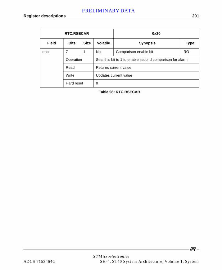
Register descriptions 201PRELIMINARY DATA
enb 7 1 No Comparison enable bit RO
Operation Sets this bit to 1 to enable second comparison for alarm
Read Returns current value
Write Updates current value
Hard reset 0
RTC.RSECAR 0x20
Field Bits Size Volatile Synopsis Type
Table 98: RTC.RSECAR
STMicroelectronicsADCS 7153464G SH-4, ST40 System Architecture, Volume 1: System

202 Register descriptionsPRELIMINARY DATA
7.2.10 Minute alarm register (RTC.RMINAR)
RTC.RMINAR is an 8-bit read/write register used as an alarm register for the RTC’s BCD-coded minute value counter, RTC.RMINCNT. When the ENB bit is set to 1, the RTC.RMINAR value is compared with the RTC.RMINCNT value. Comparison between the counter and the alarm register is performed for those registers among RTC.RSECAR, RTC.RMINAR, RTC.RHRAR, RTC.RWKAR, RTC.RDAYAR, and RTC.RMONAR in which the ENB bit is set to 1, and the RTC.RCR1 alarm flag is set when the respective values all match.
The setting range is decimal 00 to 59 + ENB bit. The RTC will not operate normally if any other value is set.
The ENB bit in RTC.RMINAR is initialized by a power-on reset. The other fields in RTC.RMINAR are not initialized by a power-on or manual reset, or in standby mode.
RTC.RMINAR 0x24
Field Bits Size Volatile Synopsis Type
units [0:3] 4 No Minute value RW
Operation 1 minute comparison value
Read Reads current value
Write Updates current value
Hard reset Undefined
tens [4:6] 3 No 10 minute value RW
Operation 1 minute comparison value
Read Reads current value
Write Updates current value
Hard reset Undefined
Table 99: RTC.RMINAR
STMicroelectronicsSH-4, ST40 System Architecture, Volume 1: System ADCS 7153464G

Register descriptions 203PRELIMINARY DATA
ENB 7 1 No Comparison enable bit RO
Operation Enables comparison for alarm
Read Returns current value
Write 1: Enable minute comparison
Hard reset 0
RTC.RMINAR 0x24
Field Bits Size Volatile Synopsis Type
Table 99: RTC.RMINAR
STMicroelectronicsADCS 7153464G SH-4, ST40 System Architecture, Volume 1: System

204 Register descriptionsPRELIMINARY DATA
7.2.11 Hour alarm register (RTC.RHRAR)
RTC.RHRAR is an 8-bit read/write register used as an alarm register for the RTC’s BCD-coded hour value counter, RTC.RHRCNT. When the ENB bit is set to 1, the RTC.RHRAR value is compared with the RTC.RHRCNT value. Comparison between the counter and the alarm register is performed for those registers among RTC.RSECAR, RTC.RMINAR, RTC.RHRAR, RTC.RWKAR, RTC.RDAYAR, and RTC.RMONAR in which the ENB bit is set to 1, and the RTC.RCR1 alarm flag is set when the respective values all match.
The setting range is decimal 00 to 23 + ENB bit. The RTC will not operate normally if any other value is set.
The ENB bit in RTC.RHRAR is initialized by a power-on reset. The other fields in RTC.RHRAR are not initialized by a power-on or manual reset, or in standby mode.
Bit 6 is always read as 0. A write to this bit is invalid, but the write value should always be 0.
RTC.RHRAR 0x28
Field Bits Size Volatile Synopsis Type
units [0:3] 4 No Hour Value RW
Operation 1 Hour comparison value
Read Reads current value
Write Updates current value
Hard reset Undefined
tens [4:5] 2 No 10 Hour Value RW
Operation 10 Hour comparison value
Read Reads current value
Write Updates current value
Hard reset Undefined
Table 100: RTC.RHRAR
STMicroelectronicsSH-4, ST40 System Architecture, Volume 1: System ADCS 7153464G

Register descriptions 205PRELIMINARY DATA
6 1 Yes Reserved RO
Operation Reserved
Read 0
Write Ignored
Hard reset 0
enb 7 1 No Comparison enable bit RO
Operation Enables hour comparison for alarm
Read Returns current value
Write 1: Enables hour comparison
Hard reset 0
RTC.RHRAR 0x28
Field Bits Size Volatile Synopsis Type
Table 100: RTC.RHRAR
STMicroelectronicsADCS 7153464G SH-4, ST40 System Architecture, Volume 1: System
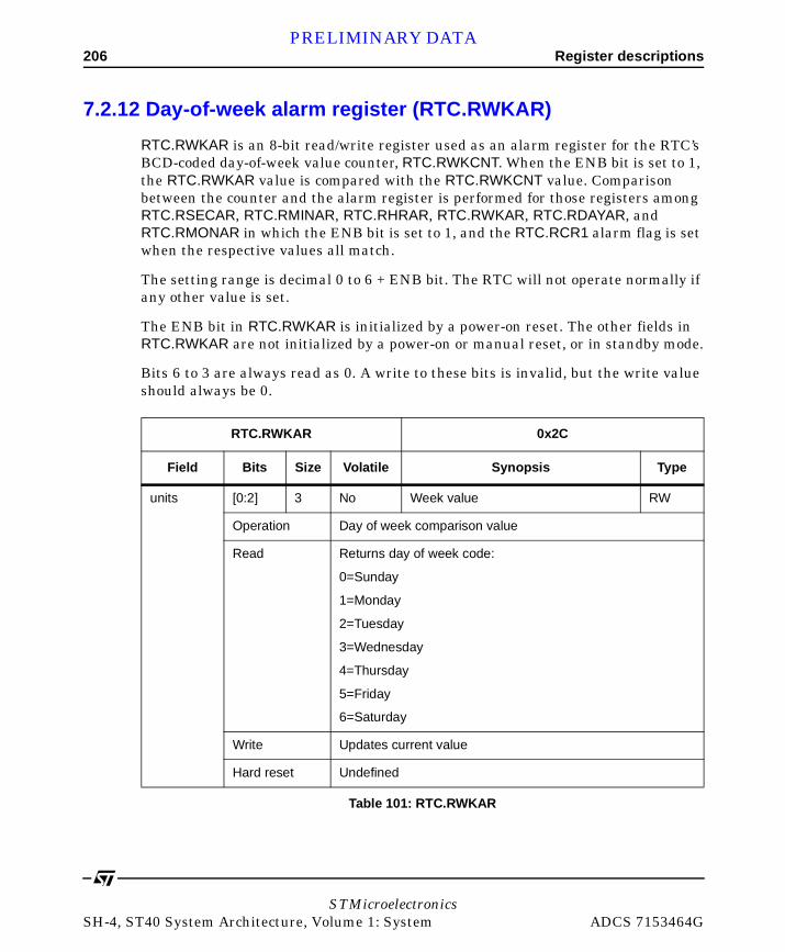
206 Register descriptionsPRELIMINARY DATA
7.2.12 Day-of-week alarm register (RTC.RWKAR)
RTC.RWKAR is an 8-bit read/write register used as an alarm register for the RTC’s BCD-coded day-of-week value counter, RTC.RWKCNT. When the ENB bit is set to 1, the RTC.RWKAR value is compared with the RTC.RWKCNT value. Comparison between the counter and the alarm register is performed for those registers among RTC.RSECAR, RTC.RMINAR, RTC.RHRAR, RTC.RWKAR, RTC.RDAYAR, and RTC.RMONAR in which the ENB bit is set to 1, and the RTC.RCR1 alarm flag is set when the respective values all match.
The setting range is decimal 0 to 6 + ENB bit. The RTC will not operate normally if any other value is set.
The ENB bit in RTC.RWKAR is initialized by a power-on reset. The other fields in RTC.RWKAR are not initialized by a power-on or manual reset, or in standby mode.
Bits 6 to 3 are always read as 0. A write to these bits is invalid, but the write value should always be 0.
RTC.RWKAR 0x2C
Field Bits Size Volatile Synopsis Type
units [0:2] 3 No Week value RW
Operation Day of week comparison value
Read Returns day of week code:
0=Sunday
1=Monday
2=Tuesday
3=Wednesday
4=Thursday
5=Friday
6=Saturday
Write Updates current value
Hard reset Undefined
Table 101: RTC.RWKAR
STMicroelectronicsSH-4, ST40 System Architecture, Volume 1: System ADCS 7153464G
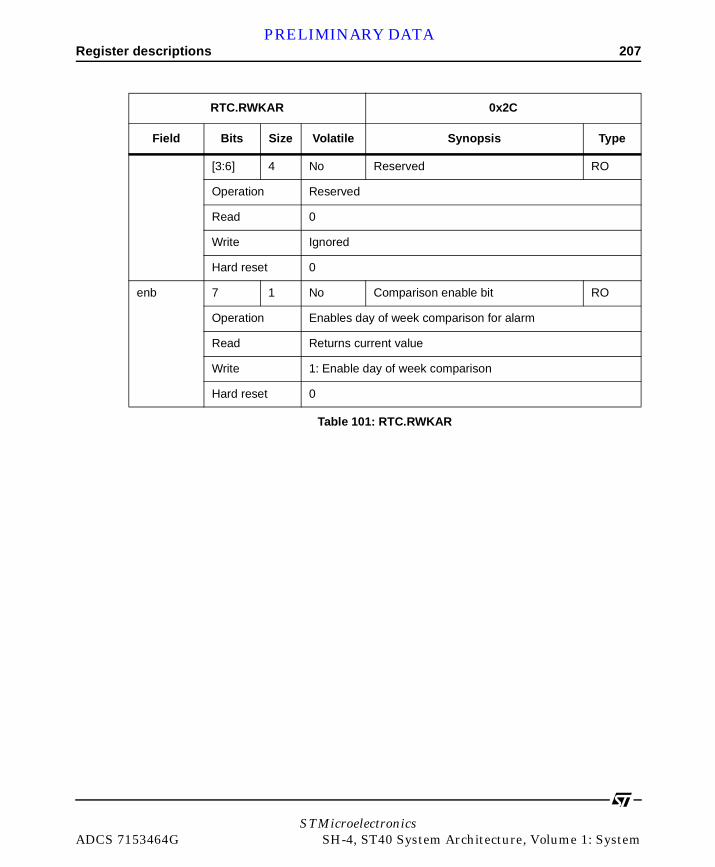
Register descriptions 207PRELIMINARY DATA
[3:6] 4 No Reserved RO
Operation Reserved
Read 0
Write Ignored
Hard reset 0
enb 7 1 No Comparison enable bit RO
Operation Enables day of week comparison for alarm
Read Returns current value
Write 1: Enable day of week comparison
Hard reset 0
RTC.RWKAR 0x2C
Field Bits Size Volatile Synopsis Type
Table 101: RTC.RWKAR
STMicroelectronicsADCS 7153464G SH-4, ST40 System Architecture, Volume 1: System
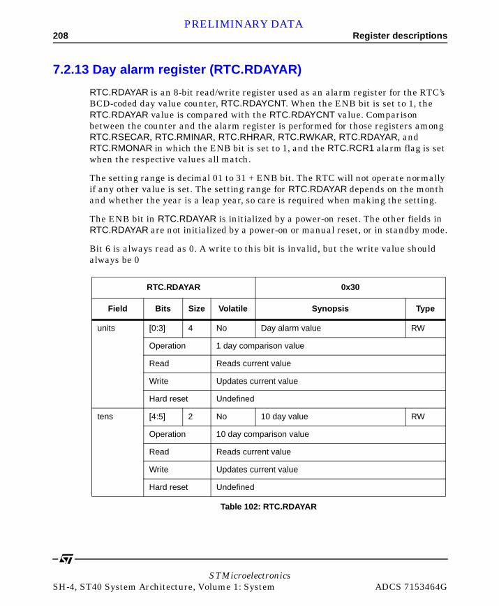
208 Register descriptionsPRELIMINARY DATA
7.2.13 Day alarm register (RTC.RDAYAR)
RTC.RDAYAR is an 8-bit read/write register used as an alarm register for the RTC’s BCD-coded day value counter, RTC.RDAYCNT. When the ENB bit is set to 1, the RTC.RDAYAR value is compared with the RTC.RDAYCNT value. Comparison between the counter and the alarm register is performed for those registers among RTC.RSECAR, RTC.RMINAR, RTC.RHRAR, RTC.RWKAR, RTC.RDAYAR, and RTC.RMONAR in which the ENB bit is set to 1, and the RTC.RCR1 alarm flag is set when the respective values all match.
The setting range is decimal 01 to 31 + ENB bit. The RTC will not operate normally if any other value is set. The setting range for RTC.RDAYAR depends on the month and whether the year is a leap year, so care is required when making the setting.
The ENB bit in RTC.RDAYAR is initialized by a power-on reset. The other fields in RTC.RDAYAR are not initialized by a power-on or manual reset, or in standby mode.
Bit 6 is always read as 0. A write to this bit is invalid, but the write value should always be 0
RTC.RDAYAR 0x30
Field Bits Size Volatile Synopsis Type
units [0:3] 4 No Day alarm value RW
Operation 1 day comparison value
Read Reads current value
Write Updates current value
Hard reset Undefined
tens [4:5] 2 No 10 day value RW
Operation 10 day comparison value
Read Reads current value
Write Updates current value
Hard reset Undefined
Table 102: RTC.RDAYAR
STMicroelectronicsSH-4, ST40 System Architecture, Volume 1: System ADCS 7153464G
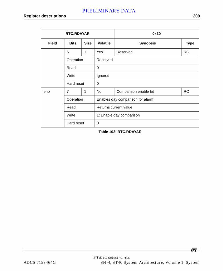
Register descriptions 209PRELIMINARY DATA
6 1 Yes Reserved RO
Operation Reserved
Read 0
Write Ignored
Hard reset 0
enb 7 1 No Comparison enable bit RO
Operation Enables day comparison for alarm
Read Returns current value
Write 1: Enable day comparison
Hard reset 0
RTC.RDAYAR 0x30
Field Bits Size Volatile Synopsis Type
Table 102: RTC.RDAYAR
STMicroelectronicsADCS 7153464G SH-4, ST40 System Architecture, Volume 1: System
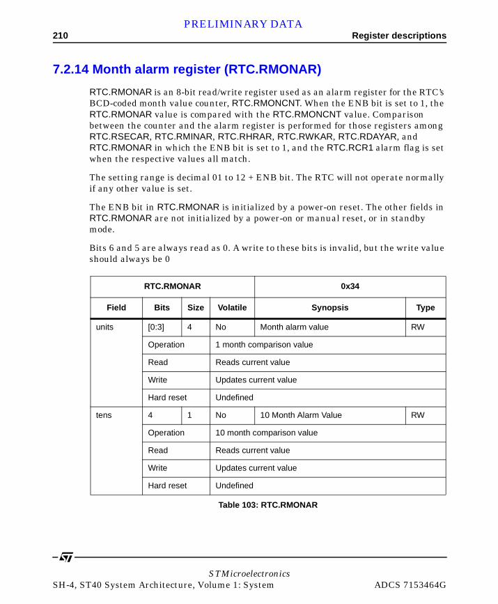
210 Register descriptionsPRELIMINARY DATA
7.2.14 Month alarm register (RTC.RMONAR)
RTC.RMONAR is an 8-bit read/write register used as an alarm register for the RTC’s BCD-coded month value counter, RTC.RMONCNT. When the ENB bit is set to 1, the RTC.RMONAR value is compared with the RTC.RMONCNT value. Comparison between the counter and the alarm register is performed for those registers among RTC.RSECAR, RTC.RMINAR, RTC.RHRAR, RTC.RWKAR, RTC.RDAYAR, and RTC.RMONAR in which the ENB bit is set to 1, and the RTC.RCR1 alarm flag is set when the respective values all match.
The setting range is decimal 01 to 12 + ENB bit. The RTC will not operate normally if any other value is set.
The ENB bit in RTC.RMONAR is initialized by a power-on reset. The other fields in RTC.RMONAR are not initialized by a power-on or manual reset, or in standby mode.
Bits 6 and 5 are always read as 0. A write to these bits is invalid, but the write value should always be 0
RTC.RMONAR 0x34
Field Bits Size Volatile Synopsis Type
units [0:3] 4 No Month alarm value RW
Operation 1 month comparison value
Read Reads current value
Write Updates current value
Hard reset Undefined
tens 4 1 No 10 Month Alarm Value RW
Operation 10 month comparison value
Read Reads current value
Write Updates current value
Hard reset Undefined
Table 103: RTC.RMONAR
STMicroelectronicsSH-4, ST40 System Architecture, Volume 1: System ADCS 7153464G
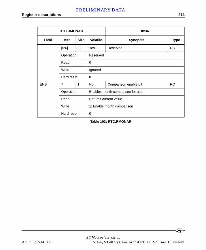
Register descriptions 211PRELIMINARY DATA
[5:6] 2 Yes Reserved RO
Operation Reserved
Read 0
Write Ignored
Hard reset 0
ENB 7 1 No Comparison enable bit RO
Operation Enables month comparison for alarm
Read Returns current value
Write 1: Enable month comparison
Hard reset 0
RTC.RMONAR 0x34
Field Bits Size Volatile Synopsis Type
Table 103: RTC.RMONAR
STMicroelectronicsADCS 7153464G SH-4, ST40 System Architecture, Volume 1: System
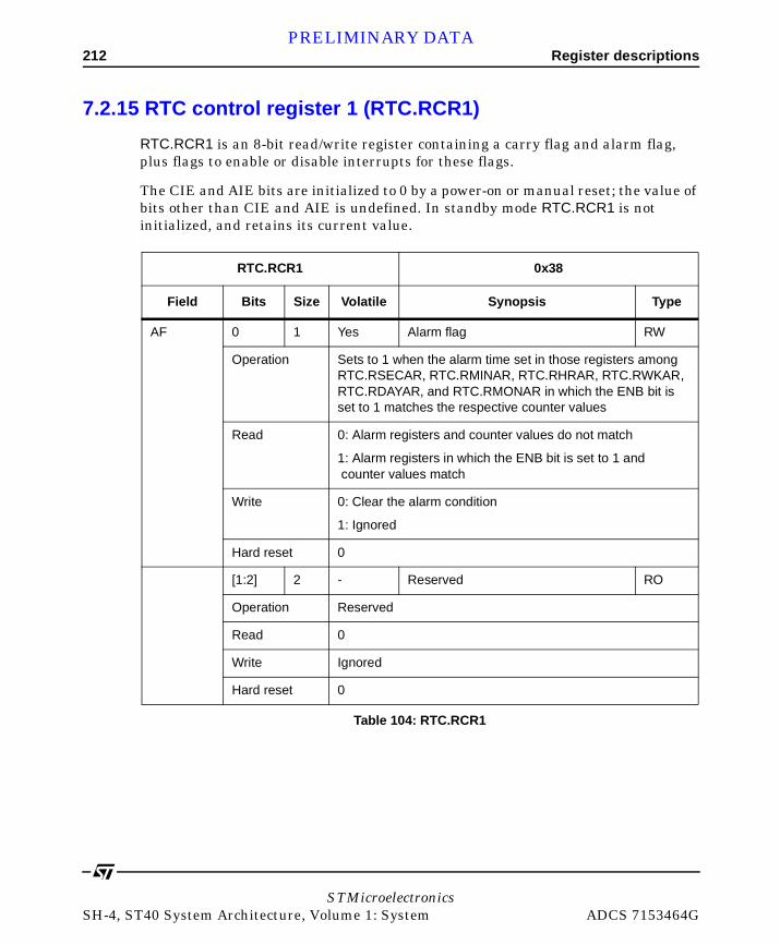
212 Register descriptionsPRELIMINARY DATA
7.2.15 RTC control register 1 (RTC.RCR1)
RTC.RCR1 is an 8-bit read/write register containing a carry flag and alarm flag, plus flags to enable or disable interrupts for these flags.
The CIE and AIE bits are initialized to 0 by a power-on or manual reset; the value of bits other than CIE and AIE is undefined. In standby mode RTC.RCR1 is not initialized, and retains its current value.
RTC.RCR1 0x38
Field Bits Size Volatile Synopsis Type
AF 0 1 Yes Alarm flag RW
Operation Sets to 1 when the alarm time set in those registers among RTC.RSECAR, RTC.RMINAR, RTC.RHRAR, RTC.RWKAR, RTC.RDAYAR, and RTC.RMONAR in which the ENB bit is set to 1 matches the respective counter values
Read 0: Alarm registers and counter values do not match
1: Alarm registers in which the ENB bit is set to 1 and counter values match
Write 0: Clear the alarm condition
1: Ignored
Hard reset 0
[1:2] 2 - Reserved RO
Operation Reserved
Read 0
Write Ignored
Hard reset 0
Table 104: RTC.RCR1
STMicroelectronicsSH-4, ST40 System Architecture, Volume 1: System ADCS 7153464G

Register descriptions 213PRELIMINARY DATA
aie 3 1 Yes Alarm interrupt enable flag RW
Operation Enables or disables interrupt generation when the alarm flag (AF) is set to 1
Read Returns current value
Write 0: Alarm interrupt is not generated when AF flag is set to 1(initial value)
1: Alarm interrupt is generated when AF flag is set to 1
Hard reset 0
cie 4 1 Yes Carry interrupt enable flag RW
Operation Enables or disables interrupt generation when the carry flag (CF) is set to 1
Read Returns current value
Write 0: Alarm interrupt is not generated when AF flag is set to 1(initial value)
1: Carry interrupt is generated when CF flag is set to 1
Hard reset 0
[5:6] 2 - Reserved RO
Operation Reserved
Read Undefined
Write Ignored
Hard reset Undefined
RTC.RCR1 0x38
Field Bits Size Volatile Synopsis Type
Table 104: RTC.RCR1
STMicroelectronicsADCS 7153464G SH-4, ST40 System Architecture, Volume 1: System
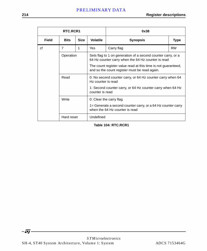
214 Register descriptionsPRELIMINARY DATA
cf 7 1 Yes Carry flag RW
Operation Sets flag to 1 on generation of a second counter carry, or a 64 Hz counter carry when the 64 Hz counter is read
The count register value read at this time is not guaranteed, and so the count register must be read again.
Read 0: No second counter carry, or 64 Hz counter carry when 64 Hz counter is read
1: Second counter carry, or 64 Hz counter carry when 64 Hz counter is read
Write 0: Clear the carry flag
1= Generate a second counter carry, or a 64 Hz counter carry when the 64 Hz counter is read
Hard reset Undefined
RTC.RCR1 0x38
Field Bits Size Volatile Synopsis Type
Table 104: RTC.RCR1
STMicroelectronicsSH-4, ST40 System Architecture, Volume 1: System ADCS 7153464G
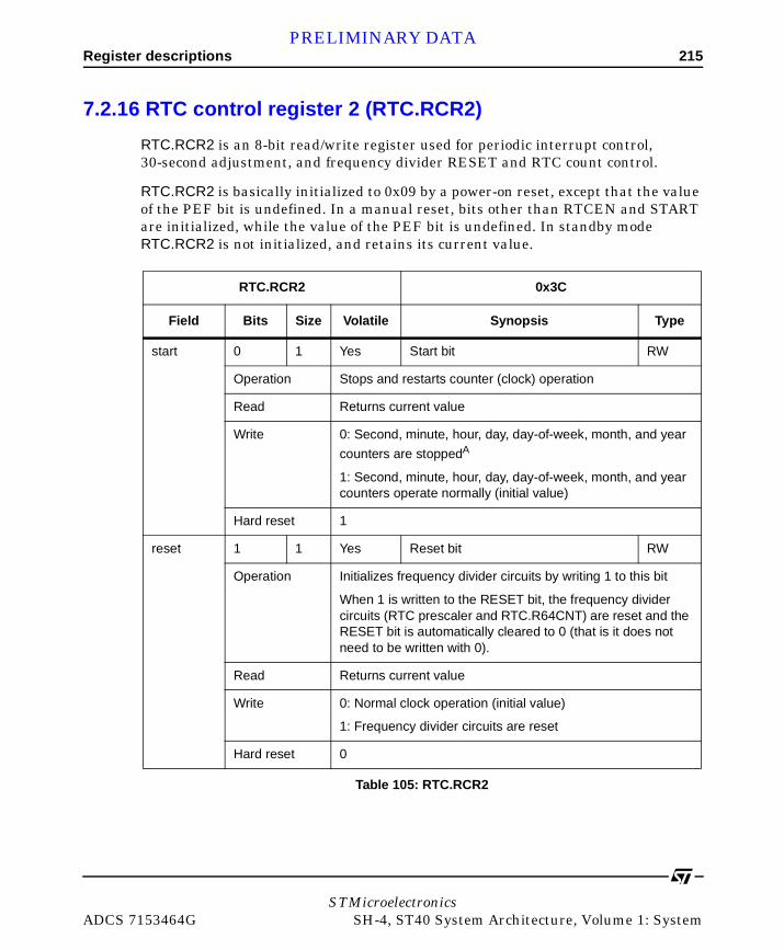
Register descriptions 215PRELIMINARY DATA
7.2.16 RTC control register 2 (RTC.RCR2)
RTC.RCR2 is an 8-bit read/write register used for periodic interrupt control, 30-second adjustment, and frequency divider RESET and RTC count control.
RTC.RCR2 is basically initialized to 0x09 by a power-on reset, except that the value of the PEF bit is undefined. In a manual reset, bits other than RTCEN and START are initialized, while the value of the PEF bit is undefined. In standby mode RTC.RCR2 is not initialized, and retains its current value.
RTC.RCR2 0x3C
Field Bits Size Volatile Synopsis Type
start 0 1 Yes Start bit RW
Operation Stops and restarts counter (clock) operation
Read Returns current value
Write 0: Second, minute, hour, day, day-of-week, month, and year
counters are stoppedA
1: Second, minute, hour, day, day-of-week, month, and year counters operate normally (initial value)
Hard reset 1
reset 1 1 Yes Reset bit RW
Operation Initializes frequency divider circuits by writing 1 to this bit
When 1 is written to the RESET bit, the frequency divider circuits (RTC prescaler and RTC.R64CNT) are reset and the RESET bit is automatically cleared to 0 (that is it does not need to be written with 0).
Read Returns current value
Write 0: Normal clock operation (initial value)
1: Frequency divider circuits are reset
Hard reset 0
Table 105: RTC.RCR2
STMicroelectronicsADCS 7153464G SH-4, ST40 System Architecture, Volume 1: System
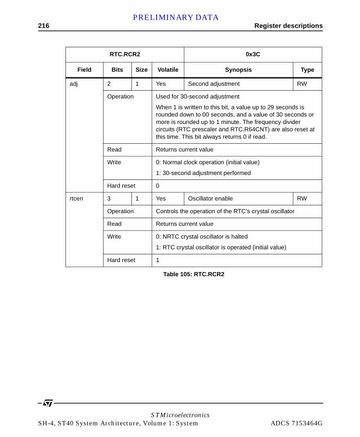
216 Register descriptionsPRELIMINARY DATA
adj 2 1 Yes Second adjustment RW
Operation Used for 30-second adjustment
When 1 is written to this bit, a value up to 29 seconds is rounded down to 00 seconds, and a value of 30 seconds or more is rounded up to 1 minute. The frequency divider circuits (RTC prescaler and RTC.R64CNT) are also reset at this time. This bit always returns 0 if read.
Read Returns current value
Write 0: Normal clock operation (initial value)
1: 30-second adjustment performed
Hard reset 0
rtcen 3 1 Yes Oscillator enable RW
Operation Controls the operation of the RTC’s crystal oscillator
Read Returns current value
Write 0: NRTC crystal oscillator is halted
1: RTC crystal oscillator is operated (initial value)
Hard reset 1
RTC.RCR2 0x3C
Field Bits Size Volatile Synopsis Type
Table 105: RTC.RCR2
STMicroelectronicsSH-4, ST40 System Architecture, Volume 1: System ADCS 7153464G

Register descriptions 217PRELIMINARY DATA
pes0, PES1,pes2
[4:6] 3 Yes Periodic interrupt enable RW
Operation Specifies the period for periodic interrupts
Read Returns current value
Write Bit 6: Bit 5: Bit 4: DescriptionPES2 PES1 PES0
0 0 0 No periodic interrupt generation (initial value)
- 1 0 Periodic interrupt generatedat 1/256-second intervals
- - 1 Periodic interrupt generatedat 1/64-second intervals
1 0 0 Periodic interrupt generated at 1/16-second intervals
- - 1 Periodic interrupt generated at 1/4-second intervals
- 1 0 Periodic interrupt generated at 1/2-second intervals
- - 1 Periodic interrupt generated at 1-second intervals
- - - Periodic interrupt generated at 2-second intervals
Hard reset 0
RTC.RCR2 0x3C
Field Bits Size Volatile Synopsis Type
Table 105: RTC.RCR2
STMicroelectronicsADCS 7153464G SH-4, ST40 System Architecture, Volume 1: System

218 Register descriptionsPRELIMINARY DATA
pef 7 1 Yes Periodic interrupt flag RW
Operation Allows interrupt generation at the interval specified by bits PES2 to PES0
Read Returns current value
Write 0: Interrupt is not generated
1: Interrupt is generated
Hard reset Undefined
A. The 64 Hz counter continues to operate unless stopped by means of the RTCEN bit.
RTC.RCR2 0x3C
Field Bits Size Volatile Synopsis Type
Table 105: RTC.RCR2
STMicroelectronicsSH-4, ST40 System Architecture, Volume 1: System ADCS 7153464G

Operation 219PRELIMINARY DATA
7.3 Operation Examples of the use of the RTC are shown below.
7.3.1 Time setting procedures
Figure 22 shows examples of the time setting procedures.
Figure 22: Examples of time-setting procedures
Stop clockReset frequency divider
Set second/minute/hour/day/day-of-week/month/year
Start clock operation
Set RCR2.RESET to 1Clear RCR2.START to 0
In any order
Set RCR2.START to 1
(a) Setting time after stopping clock
Clear carry flag
Write to counter register
Carry flag = 1?
No
Yes
Clear RCR1.CF to 0(Write 1 to RCR1.AF so that alarm flag is not cleared)
Set RYRCNT first and RSECCNT last
Read RCR1 register and check CF bit
(b) Setting time while clock is running
STMicroelectronicsADCS 7153464G SH-4, ST40 System Architecture, Volume 1: System

220 OperationPRELIMINARY DATA
The procedure for setting the time after stopping the clock is shown in the first flow diagram in Figure 22. The programming for this method is simple, and it is useful for setting all the counters, from second to year.
The procedure for setting the time while the clock is running is shown in the second flow diagram in Figure 22. This method is useful for modifying only certain counter values (for example, only the second data or hour data). If a carry occurs during the write operation, the write data is automatically updated and there will be an error in the set data. The carry flag should therefore be used to check the write status. If the carry flag (RTC.RCR1.CF) is set to 1, the write must be repeated.
The interrupt function can also be used to determine the carry flag status.
STMicroelectronicsSH-4, ST40 System Architecture, Volume 1: System ADCS 7153464G

Operation 221PRELIMINARY DATA
7.3.2 Time reading procedures
Figure 23 shows examples of the time-reading procedures.
Figure 23: Examples of time-reading procedures
Disable carry interrupts
Clear carry flag
Read counter register
Carry flag = 1?
Clear RCR1.CIE to 0
Clear RCR1.CF to 0(Write 1 to RCR1.AF so that alarm flag is not cleared)
Read RCR1 register and check CF bit
(a) Reading time without using interrupts
No
Yes
Clear carry flag
Enable carry interrupts
Clear carry flag
Read counter register
Interrupt generated?Yes
Disable carry interrupts
No
(b) Reading time using interrupts
Set RCR1.CIE to 1
Clear RCR1.CF to 0(Write 1 to RCR1.AF so that alarm flag is not cleared)
Clear RCR1.CIE to 0
STMicroelectronicsADCS 7153464G SH-4, ST40 System Architecture, Volume 1: System

222 OperationPRELIMINARY DATA
If a carry occurs while the time is being read, the correct time will not be obtained and the read must be repeated. The procedure for reading the time without using interrupts is shown in the first flow diagram, and the procedure using carry interrupts in the second flow diagram in Figure 23. The method without using interrupts is normally used to keep the program simple.
7.3.3 Alarm function
The use of the alarm function is illustrated in Figure 24.
An alarm can be generated by the second, minute, hour, day of the week, day or month value, or a combination of these. Write 1 to the ENB bit in the alarm registers involved in the alarm setting, and set the alarm time in the lower bits. Write 0 to the ENB bit in registers not involved in the alarm setting.
When the counter and the alarm time match, RTC.RCR1.AF is set to 1. Alarm detection can be confirmed by reading this bit, but normally an interrupt is used. If 1 has been written to RTC.RCR1.AIE, an alarm interrupt is generated in the event of alarm, enabling the alarm to be detected.
Figure 24: Example of use of alarm function
Clock running
Disable alarm interrupts
Set alarm time
Clear alarm flag
Enable alarm interrupts
Monitor alarm time(Wait for interrupt or check
alarm flag)
Clear RCR1.AIE to prevent erroneous interrupts
Be sure to reset the flag as it may have been set during alarm time setting
Set RCR1.AIE to 1
STMicroelectronicsSH-4, ST40 System Architecture, Volume 1: System ADCS 7153464G

Interrupts 223PRELIMINARY DATA
The alarm flag remains set while the counter and alarm time match. If the alarm flag is cleared by writing 0 during this period, it will therefore be set again immediately afterward. This needs to be taken into consideration when writing the program.
7.4 Interrupts There are 3 kinds of RTC interrupt:
• alarm interrupts,
• periodic interrupts,
• carry interrupts.
An alarm interrupt request (ATI) is generated when the alarm flag (AF) in RTC.RCR1 is set to 1 while the alarm interrupt enable bit (AIE) is also set to 1.
A periodic interrupt request (PRI) is generated when the periodic interrupt enable bits (PES2 to PES0) in RTC.RCR2 are set to a value other than 000 and the periodic interrupt flag (PEF) is set to 1.
A carry interrupt request (CUI) is generated when the carry flag (CF) in RTC.RCR1 is set to 1 while the carry interrupt enable bit (CIE) is also set to 1.
7.5 Usage notes
7.5.1 Register initialization
After powering on and making the RTC.RCR1 register settings, reset the frequency divider (by setting RTC.RCR2.RESET to 1) and make initial settings for all the other registers.
STMicroelectronicsADCS 7153464G SH-4, ST40 System Architecture, Volume 1: System

224 Usage notesPRELIMINARY DATA
7.5.2 Crystal oscillator circuit
Crystal oscillator circuit constants (recommended values) are shown in Table 106, and the RTC crystal oscillator circuit in Figure 25.
Note: 1 Select either the CIN or COUT side for the frequency adjustment variable capacitor according to requirements such as the adjustment range and degree of stability. The typical value of both CIN and COUT is 15 pF.
2 Built-in resistance value RF (typical value) = 10 MΩ, RD (typical value) = 400 kΩ
3 CIN and COUT values include floating capacitance due to the wiring. Take care when using a solid-earth board.
fosc Cin Cout
32.768 kHz 10-22 pF 10-22 pF
Table 106: Crystal oscillator circuit constants (recommended values)
Figure 25: Example of crystal oscillator circuit connection
R1RD
XTAL2EXTAL2
CIN COUTCRTC
VDD-RTC
1.8 V
ST40RA
STMicroelectronicsSH-4, ST40 System Architecture, Volume 1: System ADCS 7153464G

Usage notes 225PRELIMINARY DATA
4 The crystal oscillation stabilization time depends on the mounted circuit constants and floating capacitance and should be decided after consultation with the crystal resonator manufacturer.
5 Place the crystal resonator and load capacitors CIN and COUT as close as possible to the chip. (Correct oscillation may not be possible if there is externally induced noise in the EXTAL2 and XTAL2 pins).
6 Ensure that the crystal resonator connection pin (EXTAL2 and XTAL2) wiring is routed as far away as possible from other power lines (except GND) and signal lines.
7 The typical value of CRTC is 100 nF.
STMicroelectronicsADCS 7153464G SH-4, ST40 System Architecture, Volume 1: System

226 Usage notesPRELIMINARY DATA
STMicroelectronicsSH-4, ST40 System Architecture, Volume 1: System ADCS 7153464G

PRELIMINARY DATA
STMicroelectroniADCS 7153464G SH-4, ST40 S
8
Timer unit (TMU) 8.1 OverviewThis chapter describes the on-chip 32-bit timer unit (TMU) module comprising three 32-bit timer channels (channels 0 to 2).
8.1.1 Features
The TMU has the following features:
• auto-reload type 32-bit down-counter provided for each channel,
• input capture function provided in channel 2,
• selection of rising edge or falling edge as external clock input edge when external clock is selected or input capture function is used,
• 32-bit timer constant register for auto-reload use, read/write at any time, and 32-bit down-counter provided for each channel,
• selection of 7 counter input clocks for each channel,
- external clock (TCLK),
- on-chip RTC output clock,
- 5 internal clocks (P/4, P/16, P/64, P/256, P/1024) (P is the peripheral module clock),
• each channel can also operate in module standby mode when the on-chip RTC output clock is selected as the counter input clock, that is, timer operation continues even when the clock has been stopped for the TMU,
csystem Architecture, Volume 1: System

228 OverviewPRELIMINARY DATA
- timer count operations using an external or internal clock are only possible when a clock is supplied to the timer unit,
• synchronous read operation,1
• 2 interrupt sources,
- 1 underflow source (channels 0 to 2),
- 1 input capture source (channel 2),
• DMAC data transfer request capability,
- on channel 2, a data transfer request is sent to the DMAC when an input capture interrupt is generated.
1. As the timer counters (TCNT) are serially modified 32-bit registers and the internal peripheral module bus is 16 bits wide, there is a time difference when reading the upper 16 bits and lower 16 bits of TCNT. To prevent counter read value drift due to this time difference, a synchronization circuit is provided that allows simultaneous reading of all 32 bits of the TCNT data.
STMicroelectronicsSH-4, ST40 System Architecture, Volume 1: System ADCS 7153464G

Overview 229PRELIMINARY DATA
8.1.2 Block diagram
Figure 26 shows a block diagram of the TMU.
8.1.3 Pin configuration
Table 107 shows the TMU pins.
Figure 26: Block diagram of TMU
TUNI1 TCLK RTCCLK TUNI2 TICPI2PCLK/4, 16, 64*TUNI0
TOCR
TSTR
TCPR2TCNT2TCOR2TCR2TCNT1TCOR1TCR1TCNT0TCOR0TCR0
RESET, STBY,etc.
TMUcontrol unit
PrescalerTCLK
control unit
To each channel
Counter unit
To each channel
Interruptcontrol unit Counter unit
Interruptcontrol unit Counter unit
Interruptcontrol unit
Ch 2
Bus interface
Ch 1Ch 0
Note: * Signals with 1/4, 1/16, and 1/64 the Pφ frequency, supplied to the on-chip peripheral functions.
Internal peripheral module bus
Pin Name Abbreviation I/O Function
Clock input/clock output TCLK I/O External clock input pin/input capture control input pin
RTC output pin (shared with RTC)
Table 107: TMU pins
STMicroelectronicsADCS 7153464G SH-4, ST40 System Architecture, Volume 1: System

230 OverviewPRELIMINARY DATA
8.1.4 Register configuration
Table 108 summarizes the TMU registers. All addresses are given as offsets to the TMU base address. Refer to the system address map for the value of TMUBASE.
ChannelRegister
nameDescription Type
Address offset
Access size
Common TMU.TOCR Timer output control register,see Table 110 on page 232
RW 0x00 8
TMU.TSTR Timer start register, see Table 111 on page 233
RW 0x04 8
0 TMU.TCOR0 Timer constant register 0, see Table 112 on page 235
RW 0x08 32
TMU.TCNT0 Timer counter 0, see Table 113 on page 236
RW 0x0C 32
TMU.TCR0 Timer control register 0, see Table 114 on page 237
RW 0x10 16
1 TMU.TCOR1 Timer constant register 1, see Table 112 on page 235
RW 0x14 32
TMU.TCNT1 Timer counter 1, see Table 113 on page 236
RW 0x18 32
TMU.TCR1 Timer control register 1, see Table 114 on page 237
RW 0x1C 16
2 TMU.TCOR2 Timer constant register 2, see Table 112 on page 235
RW 0x20 32
TMU.TCNT2 Timer counter 2, see Table 113 on page 236
RW 0x24 32
TMU.TCR2 Timer control register 2, see Table 115 on page 239
RW 0x28 16
TMU.TCPR2 Input capture register, see Table 116 on page 243
RO 0x2C 32
Table 108: TMU registers
STMicroelectronicsSH-4, ST40 System Architecture, Volume 1: System ADCS 7153464G

Overview 231PRELIMINARY DATA
Register namePower-on
resetManual reset Standby mode Initial value
TMU.TOCR Initialized Initialized Held 0x00
TMU.TSTR Initialized Initialized InitializedA 0x00
TMU.TCOR0 Initialized Initialized Held 0xFFFFFFFF
TMU.TCNT0 Initialized Initialized HeldB 0xFFFFFFFF
TMU.TCR0 Initialized Initialized Held 0x0000
TMU.TCOR1 Initialized Initialized Held 0xFFFFFFFF
TMU.TCNT1 Initialized Initialized HeldA 0xFFFFFFFF
TMU.TCR1 Initialized Initialized Held 0x0000
TMU.TCOR2 Initialized Initialized Held 0xFFFFFFFF
TMU.TCNT2 Initialized Initialized HeldA 0xFFFFFFFF
TMU.TCR2 Initialized Initialized Held 0x0000
TMU.TCPR2 Held Held Held Undefined
Table 109: Initialization of TMU registers
A. Not initialized in standby mode when the input clock is the on-chip RTC output clock
B. Counts in module standby mode when the input clock is the on-chip RTC output clock.
STMicroelectronicsADCS 7153464G SH-4, ST40 System Architecture, Volume 1: System
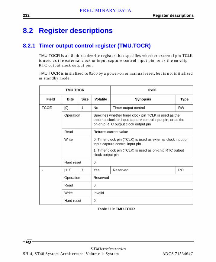
232 Register descriptionsPRELIMINARY DATA
8.2 Register descriptions
8.2.1 Timer output control register (TMU.TOCR)
TMU.TOCR is an 8-bit read/write register that specifies whether external pin TCLK is used as the external clock or input capture control input pin, or as the on-chip RTC output clock output pin.
TMU.TOCR is initialized to 0x00 by a power-on or manual reset, but is not initialized in standby mode.
TMU.TOCR 0x00
Field Bits Size Volatile Synopsis Type
TCOE [0] 1 No Timer output control RW
Operation Specifies whether timer clock pin TCLK is used as the external clock or input capture control input pin, or as the on-chip RTC output clock output pin
Read Returns current value
Write 0: Timer clock pin (TCLK) is used as external clock input or input capture control input pin
1: Timer clock pin (TCLK) is used as on-chip RTC output clock output pin
Hard reset 0
- [1:7] 7 Yes Reserved RO
Operation Reserved
Read 0
Write Invalid
Hard reset 0
Table 110: TMU.TOCR
STMicroelectronicsSH-4, ST40 System Architecture, Volume 1: System ADCS 7153464G

Register descriptions 233PRELIMINARY DATA
8.2.2 Timer start register (TMU.TSTR)
TMU.TSTR is an 8-bit read/write register that specifies whether the channel 0 to 2 timer counters (TCNT) are operated or stopped.
TMU.TSTR is initialized to 0x00 by a power-on or manual reset. In module standby mode, TMU.TSTR is not initialized when the input clock selected by each channel is the on-chip RTC output clock (RTCCLK), and is initialized only when the input clock is the external clock (TCLK) or internal clock (Pø)
TMU.TSTR 0x04
Field Bits Size Volatile Synopsis Type
STR0 [0] 1 No Counter 0 start RW
Operation Specifies whether timer counter 0 (TMU.TCNT0) is operated or stopped
Read Returns current value
Write 0: TMU.TCNT0 count operation is stopped
1: TMU.TCNT0 performs count operation
Hard reset 0
STR1 [1] 1 No Counter 1 start RW
Operation Specifies whether timer counter 1 (TMU.TCNT1) is operated or stopped
Read Returns current value
Write 0: TMU.TCNT1 count operation is stopped
1: TMU.TCNT1 performs count operation
Hard reset 0
Table 111: TMU.TSTR
STMicroelectronicsADCS 7153464G SH-4, ST40 System Architecture, Volume 1: System
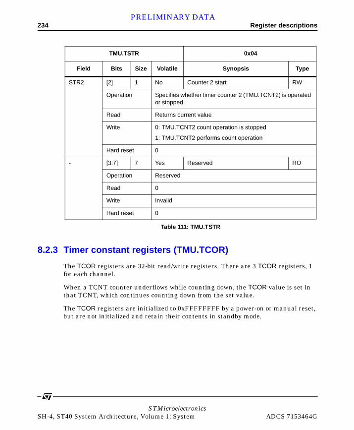
234 Register descriptionsPRELIMINARY DATA
8.2.3 Timer constant registers (TMU.TCOR)
The TCOR registers are 32-bit read/write registers. There are 3 TCOR registers, 1 for each channel.
When a TCNT counter underflows while counting down, the TCOR value is set in that TCNT, which continues counting down from the set value.
The TCOR registers are initialized to 0xFFFFFFFF by a power-on or manual reset, but are not initialized and retain their contents in standby mode.
STR2 [2] 1 No Counter 2 start RW
Operation Specifies whether timer counter 2 (TMU.TCNT2) is operated or stopped
Read Returns current value
Write 0: TMU.TCNT2 count operation is stopped
1: TMU.TCNT2 performs count operation
Hard reset 0
- [3:7] 7 Yes Reserved RO
Operation Reserved
Read 0
Write Invalid
Hard reset 0
TMU.TSTR 0x04
Field Bits Size Volatile Synopsis Type
Table 111: TMU.TSTR
STMicroelectronicsSH-4, ST40 System Architecture, Volume 1: System ADCS 7153464G

Register descriptions 235PRELIMINARY DATA
8.2.4 Timer counters (TMU.TCNT)
The TCNT registers are 32-bit read/write registers. There are 3 TCNT registers, 1 for each channel.
Each TCNT counts down on the input clock selected by TPSC2 to TPSC0 in the timer control register (TCR).
When a TCNT counter underflows while counting down, the underflow flag (UNF) is set in the corresponding timer control register (TCR). At the same time, the timer constant register (TCOR) value is set in TCNT, and the count-down operation continues from the set value.
As the TCNT registers are serially modified 32-bit registers and the internal peripheral module bus is 16 bits wide, there is a time difference when reading the upper 16 bits and lower 16 bits of TCNT. To prevent counter read value drift due to this time difference, a synchronization circuit is provided. When the upper 16 bits are read, the lower 16 bits are simultaneously stored in a buffer register. After the upper 16 bits are read, the lower 16 bits are read from the buffer register.
The TCNT registers are initialized to 0xFFFF FFFF by a power-on or manual reset, but are not initialized and retain their contents in standby mode.
TMU.TCOR[n](n = 0 to 2)
0x08 + (n * 0x0C)
Field Bits Size Volatile Synopsis Type
- [0:31] 32 No Timer constant RW
Operation Reloads TCNT [n] when it underflows
Read Returns current value
Write Updates current value
Hard reset 0xFFFF FFFF
Table 112: TMU.TCOR[n]
STMicroelectronicsADCS 7153464G SH-4, ST40 System Architecture, Volume 1: System
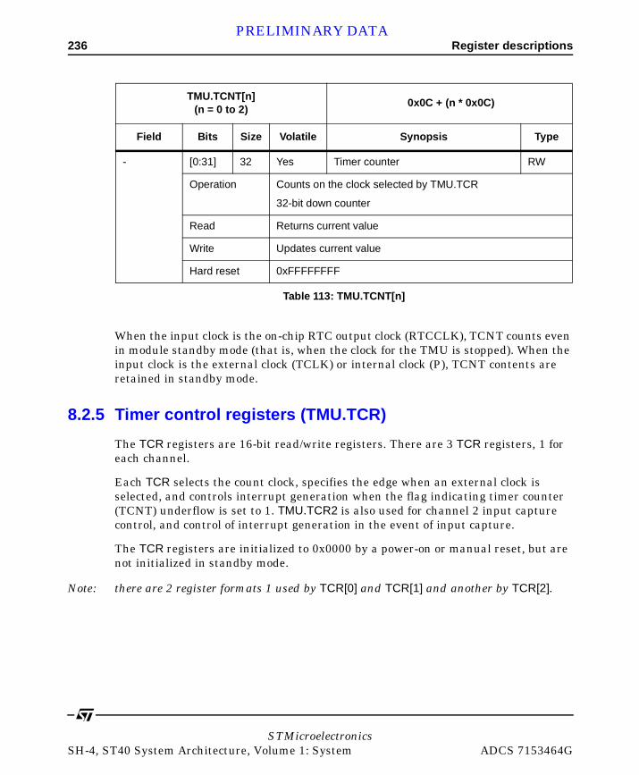
236 Register descriptionsPRELIMINARY DATA
When the input clock is the on-chip RTC output clock (RTCCLK), TCNT counts even in module standby mode (that is, when the clock for the TMU is stopped). When the input clock is the external clock (TCLK) or internal clock (P), TCNT contents are retained in standby mode.
8.2.5 Timer control registers (TMU.TCR)
The TCR registers are 16-bit read/write registers. There are 3 TCR registers, 1 for each channel.
Each TCR selects the count clock, specifies the edge when an external clock is selected, and controls interrupt generation when the flag indicating timer counter (TCNT) underflow is set to 1. TMU.TCR2 is also used for channel 2 input capture control, and control of interrupt generation in the event of input capture.
The TCR registers are initialized to 0x0000 by a power-on or manual reset, but are not initialized in standby mode.
Note: there are 2 register formats 1 used by TCR[0] and TCR[1] and another by TCR[2].
TMU.TCNT[n](n = 0 to 2)
0x0C + (n * 0x0C)
Field Bits Size Volatile Synopsis Type
- [0:31] 32 Yes Timer counter RW
Operation Counts on the clock selected by TMU.TCR
32-bit down counter
Read Returns current value
Write Updates current value
Hard reset 0xFFFFFFFF
Table 113: TMU.TCNT[n]
STMicroelectronicsSH-4, ST40 System Architecture, Volume 1: System ADCS 7153464G
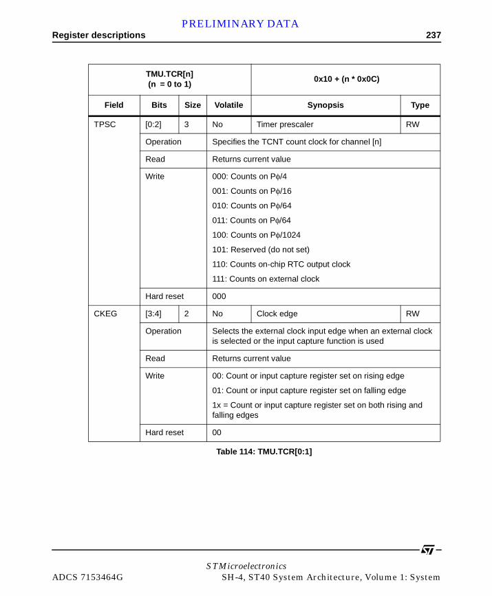
Register descriptions 237PRELIMINARY DATA
TMU.TCR[n](n = 0 to 1)
0x10 + (n * 0x0C)
Field Bits Size Volatile Synopsis Type
TPSC [0:2] 3 No Timer prescaler RW
Operation Specifies the TCNT count clock for channel [n]
Read Returns current value
Write 000: Counts on Pφ/4
001: Counts on Pφ/16
010: Counts on Pφ/64
011: Counts on Pφ/64
100: Counts on Pφ/1024
101: Reserved (do not set)
110: Counts on-chip RTC output clock
111: Counts on external clock
Hard reset 000
CKEG [3:4] 2 No Clock edge RW
Operation Selects the external clock input edge when an external clock is selected or the input capture function is used
Read Returns current value
Write 00: Count or input capture register set on rising edge
01: Count or input capture register set on falling edge
1x = Count or input capture register set on both rising and falling edges
Hard reset 00
Table 114: TMU.TCR[0:1]
STMicroelectronicsADCS 7153464G SH-4, ST40 System Architecture, Volume 1: System

238 Register descriptionsPRELIMINARY DATA
UNIE [5] 1 No Underflow interrupt control RW
Operation Controls enabling or disabling of interrupt generation when the UNF status flag is set to 1, indicating TCNT underflow
Read Returns current value
Write 0: Interrupt due to underflow (TUNI) is not enabled
1: Interrupt due to underflow (TUNI) is enabled
Hard reset 0
- [6:7] 2 - Reserved RO
Operation Reserved
Read 0
Write Ignored
Hard reset 0
UNF [8] 1 Yes Underflow flag RW
Operation Status flag that indicates the occurrence of underflow
Read 0= TCNT has not underflowed
1= TCNT has underflowed
Write 0= Clears flag to 0
1= Write ignored
Hard reset 0
- [9:15] 7 - Reserved RO
Operation Reserved
Read 0
Write Invalid
Hard reset 0
TMU.TCR[n](n = 0 to 1)
0x10 + (n * 0x0C)
Field Bits Size Volatile Synopsis Type
Table 114: TMU.TCR[0:1]
STMicroelectronicsSH-4, ST40 System Architecture, Volume 1: System ADCS 7153464G
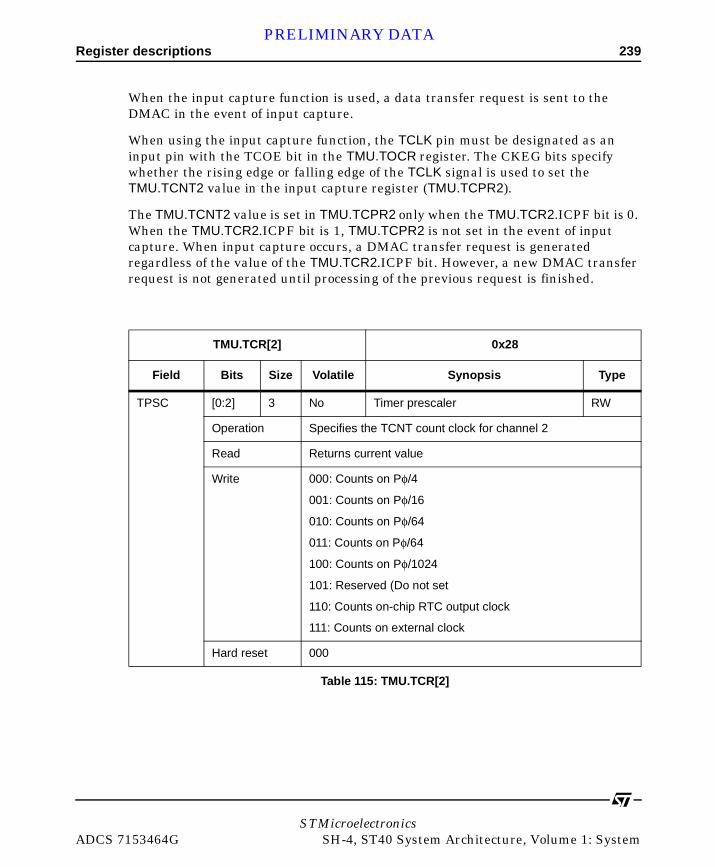
Register descriptions 239PRELIMINARY DATA
When the input capture function is used, a data transfer request is sent to the DMAC in the event of input capture.
When using the input capture function, the TCLK pin must be designated as an input pin with the TCOE bit in the TMU.TOCR register. The CKEG bits specify whether the rising edge or falling edge of the TCLK signal is used to set the TMU.TCNT2 value in the input capture register (TMU.TCPR2).
The TMU.TCNT2 value is set in TMU.TCPR2 only when the TMU.TCR2.ICPF bit is 0. When the TMU.TCR2.ICPF bit is 1, TMU.TCPR2 is not set in the event of input capture. When input capture occurs, a DMAC transfer request is generated regardless of the value of the TMU.TCR2.ICPF bit. However, a new DMAC transfer request is not generated until processing of the previous request is finished.
TMU.TCR[2] 0x28
Field Bits Size Volatile Synopsis Type
TPSC [0:2] 3 No Timer prescaler RW
Operation Specifies the TCNT count clock for channel 2
Read Returns current value
Write 000: Counts on Pφ/4
001: Counts on Pφ/16
010: Counts on Pφ/64
011: Counts on Pφ/64
100: Counts on Pφ/1024
101: Reserved (Do not set
110: Counts on-chip RTC output clock
111: Counts on external clock
Hard reset 000
Table 115: TMU.TCR[2]
STMicroelectronicsADCS 7153464G SH-4, ST40 System Architecture, Volume 1: System
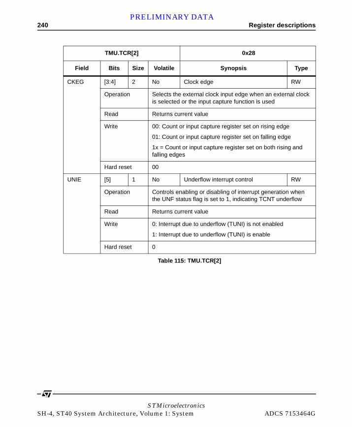
240 Register descriptionsPRELIMINARY DATA
CKEG [3:4] 2 No Clock edge RW
Operation Selects the external clock input edge when an external clock is selected or the input capture function is used
Read Returns current value
Write 00: Count or input capture register set on rising edge
01: Count or input capture register set on falling edge
1x = Count or input capture register set on both rising and falling edges
Hard reset 00
UNIE [5] 1 No Underflow interrupt control RW
Operation Controls enabling or disabling of interrupt generation when the UNF status flag is set to 1, indicating TCNT underflow
Read Returns current value
Write 0: Interrupt due to underflow (TUNI) is not enabled
1: Interrupt due to underflow (TUNI) is enable
Hard reset 0
TMU.TCR[2] 0x28
Field Bits Size Volatile Synopsis Type
Table 115: TMU.TCR[2]
STMicroelectronicsSH-4, ST40 System Architecture, Volume 1: System ADCS 7153464G

Register descriptions 241PRELIMINARY DATA
ICPE [6:7] 2 No Input capture control RW
Operation Specifies whether the input capture function is used, and control enabling or disabling of interrupt generation when the function is used
Read Returns current value
Write 00: Input capture function not used
01: Reserved (do not set)
10: Input capture function used, but interrupt due to input capture (TICPI2) not enabled
Data transfer request is sent to DMAC in the event of input capture
11: Input capture function used, and interrupt due to input capture (TICPI2) enabled
Data transfer request is sent to DMAC in the event of input capture
Hard reset 0
UNF [8] 1 Yes Underflow flag RW
Operation Indicates the occurrence of underflow
Read 0: TCNT has not underflowed
1: TCNT has underflowed
Write 0: Clear flag to 0
1= Ignored
Hard reset 0
TMU.TCR[2] 0x28
Field Bits Size Volatile Synopsis Type
Table 115: TMU.TCR[2]
STMicroelectronicsADCS 7153464G SH-4, ST40 System Architecture, Volume 1: System

242 Register descriptionsPRELIMINARY DATA
ICPF [9] 1 Yes Input capture interrupt flag RW
Operation Indicates the occurrence of input capture
This status flag is provided in channel 2 only.
Read 0: Input capture has not occurred
1: Input capture has occurred
Write 0: Clear flag to 0
1: Ignored
Hard reset 0
- [10:15] 6 No Reserved RO
Operation Reserved
Read 0
Write Invalid
Hard reset 0
TMU.TCR[2] 0x28
Field Bits Size Volatile Synopsis Type
Table 115: TMU.TCR[2]
STMicroelectronicsSH-4, ST40 System Architecture, Volume 1: System ADCS 7153464G

Register descriptions 243PRELIMINARY DATA
8.2.6 Input capture register (TMU.TCPR2)
TMU.TCPR2 is a 32-bit read-only register for use with the input capture function, provided only in channel 2.
The input capture function is controlled by means of the input capture control bits (ICPE1, ICPE0) and clock edge bits (CKEG1, CKEG0) in TMU.TCR2. When input capture occurs, the TMU.TCNT2 value is copied into TMU.TCPR2. The value is set in TMU.TCPR2 only when the ICPF bit in TMU.TCR2 is 0.
TMU.TCPR2 is not initialized by a power-on or manual reset, or in standby mode.
TMU.TCPR2 0x2C
Field Bits Size Volatile Synopsis Type
[0:31] 32 No Input capture value RO
Operation Gives the value of TMU.TCNT2 when capture occurs
Read Returns current value
Write Ignored
Hard reset 0xFFFFFFFF
Table 116: TMU.TCPR2
STMicroelectronicsADCS 7153464G SH-4, ST40 System Architecture, Volume 1: System
244 OperationPRELIMINARY DATA
8.3 OperationEach channel has a 32-bit timer counter (TCNT) that performs count-down operations, and a 32-bit timer constant register (TCOR). The channels have an auto- reload function that allows cyclic count operations, and can also perform external event counting. Channel 2 also has an input capture function.
8.3.1 Counter operation
When 1 of bits STR0 to STR2 is set to 1 in the timer start register (TMU.TSTR), the timer counter (TCNT) for the corresponding channel starts counting. When TCNT underflows, the UNF flag is set in the corresponding timer control register (TCR). If the UNIE bit in TCR is set to 1 at this time, an interrupt request is sent to the CPU. At the same time, the value is copied from TCOR into TCNT, and the count-down continues (auto-reload function).
Example of count operation setting procedure
Figure 27 shows an example of the count operation setting procedure.
1 Select the count clock with bits TPSC2 to TPSC0 in the timer control register (TCR). When an external clock is selected, set the TCLK pin to input mode with the TCOE bit in TMU.TOCR, and select the external clock edge with bits CKEG1 and CKEG0 in TCR.
2 Specify whether an interrupt is to be generated on TCNT underflow with the UNIE bit in TCR.
3 When the input capture function is used, set the ICPE bits in TCR, including specification of whether the interrupt function is to be used.
4 Set a value in the timer constant register (TCOR).
5 Set the initial value in the timer counter (TCNT).
6 Set the STR bit to 1 in the timer start register (TMU.TSTR) to start the count
.
STMicroelectronicsSH-4, ST40 System Architecture, Volume 1: System ADCS 7153464G

Operation 245PRELIMINARY DATA
Figure 27: Example of count operation setting procedure
1
2
Operation selection
Select count clock
Underflow interruptgeneration setting
When input capture function is used
3
4
5
6
Input capture interruptgeneration setting
Timer constantregister setting
Set initial timercounter value
Start count
Note: When an interrupt is generated, clear the source flag in the interrupt handler. If the interrupt enabled state is set without clearing the flag, another interrupt will be generated.
STMicroelectronicsADCS 7153464G SH-4, ST40 System Architecture, Volume 1: System

246 OperationPRELIMINARY DATA
Auto-reload count operation
Figure 28 shows the TCNT auto-reload operation.
TCNT count timing
Operating on internal clock
Any of 5 count clocks (Pø/4, Pø/16, Pø/64, Pø/256, or Pø/1024) scaled from the peripheral module clock can be selected as the count clock by means of the TPSC2 to TPSC0 bits in TCR.
Figure 29 shows the timing in this case.
Figure 28: TCNT auto-reload operation
TCOR
H'00000000
STR0–STR2
UNF
TCNT value TCOR value set in TCNT on underflow
Time
Figure 29: Count timing when operating on internal clock
Pφ
Internal clock
TCNT N + 1 N N – 1
STMicroelectronicsSH-4, ST40 System Architecture, Volume 1: System ADCS 7153464G

Operation 247PRELIMINARY DATA
Operating on external clock
External clock pin (TCLK) input can be selected as the timer clock by means of the TPSC2 to TPSC0 bits in TCR. The detected edge (rising, falling, or both edges) can be selected with the CKEG1 and CKEG0 bits in TCR. Figure 30 shows the timing for both-edge detection.
Operating on-chip RTC output clock
The on-chip RTC output clock can be selected as the timer clock by means of the TPSC2 to TPSC0 bits in TCR. Figure 31 shows the timing in this case.
Figure 30: Count timing when operating on external clock
Figure 31: Count timing when operating on on-chip RTC output clock
N + 1 N – 1N
Pφ
External clockinput pin
TCNT
N + 1 N N – 1
RTC output clock
TCNT
STMicroelectronicsADCS 7153464G SH-4, ST40 System Architecture, Volume 1: System
248 OperationPRELIMINARY DATA
8.3.2 Input capture function
Channel 2 has an input capture function.
The procedure for using the input capture function follows.
1 Use the TCOE bit in the timer output control register (TMU.TOCR) to set the TCLK pin to input mode.
2 Use bits TPSC2 to TPSC0 in the timer control register (TCR) to set an internal clock or the on-chip RTC output clock as the timer operating clock.
3 Use bits IPCE1 and IPCE0 in TCR to specify use of the input capture function, and whether interrupts are to generated when this function is used.
4 Use bits CKEG1 and CKEG0 in TCR to specify whether the rising or falling edge of the TCLK signal is to be used to set the timer counter (TCNT) value in the input capture register (TMU.TCPR2).
This function cannot be used in standby mode.
When input capture occurs, the TMU.TCNT2 value is set in TMU.TCPR2 only when the ICPF bit in TMU.TCR2 is 0. Also, a new DMAC transfer request is not generated until processing of the previous request is finished.
Figure 32 shows the operation timing when the input capture function is used (with TCLK rising edge detection).
STMicroelectronicsSH-4, ST40 System Architecture, Volume 1: System ADCS 7153464G

Interrupts 249PRELIMINARY DATA
8.4 Interrupts There are 4 TMU interrupt sources, comprising underflow interrupts and the input capture interrupt (when the input capture function is used). Underflow interrupts are generated on channels 0 to 2, and input capture interrupts on channel 2 only.
An underflow interrupt request is generated (for each channel) according to the AND of UNF and the interrupt enable bit (UNIE) in TCR.
When the input capture function is used and an input capture request is generated, an interrupt is requested if the input capture input flag (ICPF) in TMU.TCR2 is 1 and the input capture control bits (ICPE1, ICPE0) in TMU.TCR2 are 11.
The TMU interrupt sources are summarized in Table 117.
Figure 32: Operation timing when using input capture function
TCOR
H'00000000
TCLK
TCPR2
TICPI2
TCNT valueTCOR value set in TCNT on underflow
TCNT value set
Time
STMicroelectronicsADCS 7153464G SH-4, ST40 System Architecture, Volume 1: System
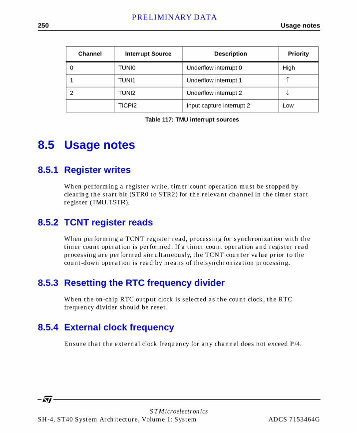
250 Usage notesPRELIMINARY DATA
8.5 Usage notes
8.5.1 Register writes
When performing a register write, timer count operation must be stopped by clearing the start bit (STR0 to STR2) for the relevant channel in the timer start register (TMU.TSTR).
8.5.2 TCNT register reads
When performing a TCNT register read, processing for synchronization with the timer count operation is performed. If a timer count operation and register read processing are performed simultaneously, the TCNT counter value prior to the count-down operation is read by means of the synchronization processing.
8.5.3 Resetting the RTC frequency divider
When the on-chip RTC output clock is selected as the count clock, the RTC frequency divider should be reset.
8.5.4 External clock frequency
Ensure that the external clock frequency for any channel does not exceed P/4.
Channel Interrupt Source Description Priority
0 TUNI0 Underflow interrupt 0 High
1 TUNI1 Underflow interrupt 1 ↑
2 TUNI2 Underflow interrupt 2 ↓
TICPI2 Input capture interrupt 2 Low
Table 117: TMU interrupt sources
STMicroelectronicsSH-4, ST40 System Architecture, Volume 1: System ADCS 7153464G

PRELIMINARY DATA
STMicroelectroniADCS 7153464G SH-4, ST40 S
9 IFO
Serial communicationinterface with F(SCIF)
9.1 OverviewThis chapter describes a single-channel serial communication interface module with built-in FIFO registers (SCIF). The SCIF can perform asynchronous serial communication.
16 stage FIFO registers are provided for both transmission and reception, enabling fast, efficient, and continuous communication.
9.1.1 Features
SCIF features are listed below.
• Asynchronous serial communication in which synchronization is achieved character by character. Serial data communication can be carried out with standard asynchronous communication chips such as UART or ACIA.
There is a choice of eight serial data transfer formats:
- data length: 7 or 8 bits,
- stop bit length: 1 or 2 bits
- parity: even, odd or none.
csystem Architecture, Volume 1: System

252 OverviewPRELIMINARY DATA
• Receive error detection:
- parity,
- framing,
- overrun errors.
• Break detection: if the receive data following that in which a framing error occurred is also at the space 0 level, and there is a frame error, a break is detected. When a framing error occurs, a break can also be detected by reading the RXD pin level directly from the serial port register (SCIF.SCSPTR).
• Full duplex communication capability: the transmitter and receiver are independent units, enabling transmission and reception to be performed simultaneously.
The transmitter and receiver both have a 16 stage FIFO buffer structure, enabling fast and continuous serial data transmission and reception.
• On-chip baud rate generator allows any bit rate to be selected.
• Choice of serial clock source: internal clock from baud rate generator or external clock from SCK pin.
• 4 interrupt sources: there are 4 interrupt sources that can issue requests independently:
- TRANSMIT-FIFO-DATA-EMPTY,
- BREAK,
- RECEIVE-FIFO-DATA-FULL,
- RECEIVE-ERROR.
• The DMA controller (DMAC) can be activated to execute a data transfer by issuing a DMA transfer request in the event of a TRANSMIT-FIFO-DATA-EMPTY or RECEIVE-FIFO-DATA-FULL interrupt.
• When not in use, the SCIF can be stopped by halting its clock supply to reduce power consumption.
• Modem control functions (RTS and CTS) are provided.
• The amount of data in the transmit and receive FIFO registers, and the number of receive errors in the receive data in the receive FIFO register, can be ascertained.
• A TIME-OUT ERROR (DR) can be detected during reception.
STMicroelectronicsSH-4, ST40 System Architecture, Volume 1: System ADCS 7153464G
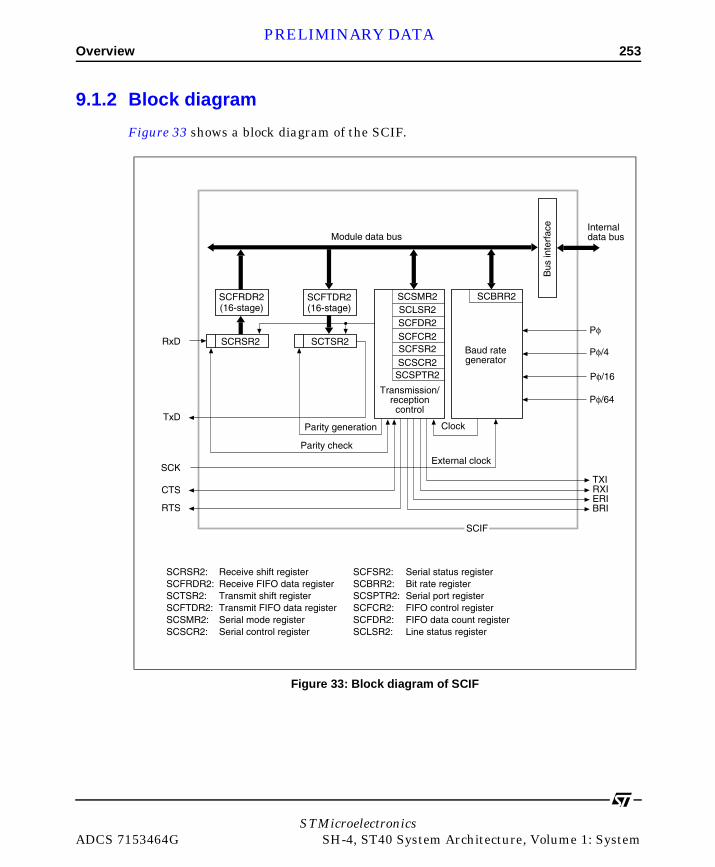
Overview 253PRELIMINARY DATA
9.1.2 Block diagram
Figure 33 shows a block diagram of the SCIF.
Figure 33: Block diagram of SCIF
Module data bus
SCFRDR2(16-stage)
SCRSR2RxD2
TxD2
SCK2
CTS2
RTS2
SCFTDR2(16-stage)
SCTSR2
SCSMR2SCLSR2SCFDR2SCFCR2SCFSR2
SCBRR2
Parity generation
Parity check
Transmission/receptioncontrol
Baud rategenerator
Clock
External clock
Pφ
Pφ/4
Pφ/16
Pφ/64
TXIRXIERIBRI
SCIF
Bus
inte
rfac
e Internal data bus
SCSCR2SCSPTR2
SCRSR2: Receive shift registerSCFRDR2: Receive FIFO data registerSCTSR2: Transmit shift registerSCFTDR2: Transmit FIFO data registerSCSMR2: Serial mode registerSCSCR2: Serial control register
SCFSR2: Serial status registerSCBRR2: Bit rate registerSCSPTR2: Serial port registerSCFCR2: FIFO control registerSCFDR2: FIFO data count registerSCLSR2: Line status register
STMicroelectronicsADCS 7153464G SH-4, ST40 System Architecture, Volume 1: System
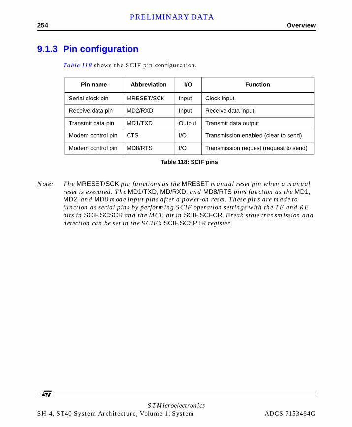
254 OverviewPRELIMINARY DATA
9.1.3 Pin configuration
Table 118 shows the SCIF pin configuration.
Note: The MRESET/SCK pin functions as the MRESET manual reset pin when a manual reset is executed. The MD1/TXD, MD/RXD, and MD8/RTS pins function as the MD1, MD2, and MD8 mode input pins after a power-on reset. These pins are made to function as serial pins by performing SCIF operation settings with the TE and RE bits in SCIF.SCSCR and the MCE bit in SCIF.SCFCR. Break state transmission and detection can be set in the SCIF’s SCIF.SCSPTR register.
Pin name Abbreviation I/O Function
Serial clock pin MRESET/SCK Input Clock input
Receive data pin MD2/RXD Input Receive data input
Transmit data pin MD1/TXD Output Transmit data output
Modem control pin CTS I/O Transmission enabled (clear to send)
Modem control pin MD8/RTS I/O Transmission request (request to send)
Table 118: SCIF pins
STMicroelectronicsSH-4, ST40 System Architecture, Volume 1: System ADCS 7153464G
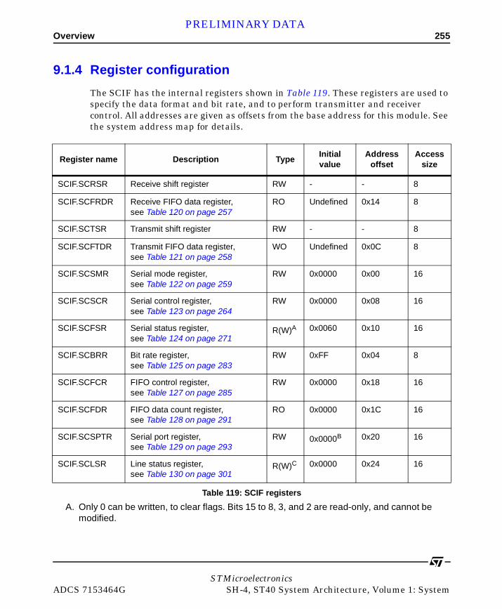
Overview 255PRELIMINARY DATA
9.1.4 Register configuration
The SCIF has the internal registers shown in Table 119. These registers are used to specify the data format and bit rate, and to perform transmitter and receiver control. All addresses are given as offsets from the base address for this module. See the system address map for details.
Register name Description TypeInitial value
Address offset
Access size
SCIF.SCRSR Receive shift register RW - - 8
SCIF.SCFRDR Receive FIFO data register, see Table 120 on page 257
RO Undefined 0x14 8
SCIF.SCTSR Transmit shift register RW - - 8
SCIF.SCFTDR Transmit FIFO data register, see Table 121 on page 258
WO Undefined 0x0C 8
SCIF.SCSMR Serial mode register, see Table 122 on page 259
RW 0x0000 0x00 16
SCIF.SCSCR Serial control register,see Table 123 on page 264
RW 0x0000 0x08 16
SCIF.SCFSR Serial status register,see Table 124 on page 271
R(W)A 0x0060 0x10 16
SCIF.SCBRR Bit rate register, see Table 125 on page 283
RW 0xFF 0x04 8
SCIF.SCFCR FIFO control register, see Table 127 on page 285
RW 0x0000 0x18 16
SCIF.SCFDR FIFO data count register, see Table 128 on page 291
RO 0x0000 0x1C 16
SCIF.SCSPTR Serial port register, see Table 129 on page 293
RW 0x0000B 0x20 16
SCIF.SCLSR Line status register, see Table 130 on page 301
R(W)C 0x0000 0x24 16
Table 119: SCIF registers
A. Only 0 can be written, to clear flags. Bits 15 to 8, 3, and 2 are read-only, and cannot be modified.
STMicroelectronicsADCS 7153464G SH-4, ST40 System Architecture, Volume 1: System

256 Register descriptionsPRELIMINARY DATA
9.2 Register descriptionsThis section describes all register states for the SCIF module.
Note: all addresses are given as offsets from the base address for this module. See the system address map for details.
9.2.1 Receive shift register (SCIF.SCRSR)
SCIF.SCRSR is the register used to receive serial data.
The SCIF sets serial data input from the RXD pin in SCIF.SCRSR in the order received, starting with the LSB (bit 0), and converts it to parallel data. When 1one byte of data has been received, it is transferred to the receive FIFO register, SCIF.SCFRDR, automatically.
SCIF.SCRSR cannot be directly read or written to by the CPU.
9.2.2 Receive FIFO data register (SCIF.SCFRDR)
SCIF.SCFRDR is a 16 stage FIFO register that stores received serial data.
When the SCIF has received 1 byte of serial data, it transfers the received data from SCIF.SCRSR to SCIF.SCFRDR where it is stored, and completes the receive operation. SCIF.SCRSR is then enabled for reception, and consecutive receive operations can be performed until the receive FIFO register is full (16 data bytes).
SCIF.SCFRDR is a read-only register, and cannot be written to by the CPU.
If a read is performed when there is no receive data in the receive FIFO register, an undefined value will be returned. When the receive FIFO register is full of receive
B. The value of bits 6, 4 and 0 is undefined.
C. Only 0 can be written, to clear flags. Bits 15 to 1 are read-only, and cannot be modified.
Bit 7 6 5 4 3 2 1 0
RW - - - - - - - -
STMicroelectronicsSH-4, ST40 System Architecture, Volume 1: System ADCS 7153464G

Register descriptions 257PRELIMINARY DATA
data, subsequent serial data is lost. The contents of SCIF.SCFRDR are undefined after a power-on reset or manual reset.
9.2.3 Transmit shift register (SCIF.SCTSR)
SCIF.SCTSR is the register used to transmit serial data.
To perform serial data transmission, the SCIF first transfers transmit data from SCIF.SCFTDR to SCIF.SCTSR, then sends the data to the TXD pin starting with the LSB (bit 0).
When transmission of 1 byte is completed, the next transmit data is transferred from SCIF.SCFTDR to SCIF.SCTSR, and transmission started, automatically.
SCIF.SCTSR cannot be directly read or written to by the CPU.
SCIF.SCFRDR 0x14
Field Bits Size Volatile Synopsis Type
SCIF.SCFRDR
[0:7] 8 Yes 16-byte receive FIFO data register RO
Operation Holds data transferred from the SCIF.SCRSR register
Read Returns and removes the next data item in the FIFO
If the FIFO is empty an undefined value is returned.
Write Invalid
Hard reset Undefined
Table 120: SCIF.SCFRDR
Bit 7 6 5 4 3 2 1 0
RW — — — — — — — —
STMicroelectronicsADCS 7153464G SH-4, ST40 System Architecture, Volume 1: System

258 Register descriptionsPRELIMINARY DATA
9.2.4 Transmit FIFO data register (SCIF.SCFTDR)
SCIF.SCFTDR is a 16 stage FIFO register that stores data for serial transmission.
If SCIF.SCTSR is empty when transmit data has been written to SCIF.SCFTDR, the SCIF transfers the transmit data written in SCIF.SCFTDR to SCIF.SCTSR and starts serial transmission.
SCIF.SCFTDR is a write-only register, and cannot be read by the CPU.
The next data cannot be written when SCIF.SCFTDR is filled with 16 bytes of transmit data. Data written in this case is ignored. The contents of SCIF.SCFTDR are undefined after a power-on reset or manual reset.
SCIF.SCFTDR 0x0C
Field Bits Size Volatile Synopsis Type
SCFTDR [0:7] 8 Yes 16-byte transmit FIFO data register WO
Operation Stores data for serial transmission
Read Invalid
Write Appends data to the FIFO register to be copied to SCIF.SCTSR
If the FIFO is full the write is ignored.
Hard reset Undefined
Table 121: SCIF.SCFTDR
STMicroelectronicsSH-4, ST40 System Architecture, Volume 1: System ADCS 7153464G
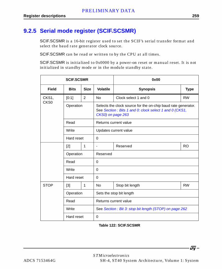
Register descriptions 259PRELIMINARY DATA
9.2.5 Serial mode register (SCIF.SCSMR)
SCIF.SCSMR is a 16-bit register used to set the SCIF’s serial transfer format and select the baud rate generator clock source.
SCIF.SCSMR can be read or written to by the CPU at all times.
SCIF.SCSMR is initialized to 0x0000 by a power-on reset or manual reset. It is not initialized in standby mode or in the module standby state.
SCIF.SCSMR 0x00
Field Bits Size Volatile Synopsis Type
CKS1, CKS0
[0:1] 2 No Clock select 1 and 0 RW
Operation Selects the clock source for the on-chip baud rate generator. See Section : Bits 1 and 0: clock select 1 and 0 (CKS1, CKS0) on page 263
Read Returns current value
Write Updates current value
Hard reset 0
[2] 1 - Reserved RO
Operation Reserved
Read 0
Write 0
Hard reset 0
STOP [3] 1 No Stop bit length RW
Operation Sets the stop bit length
Read Returns current value
Write See Section : Bit 3: stop bit length (STOP) on page 262
Hard reset 0
Table 122: SCIF.SCSMR
STMicroelectronicsADCS 7153464G SH-4, ST40 System Architecture, Volume 1: System
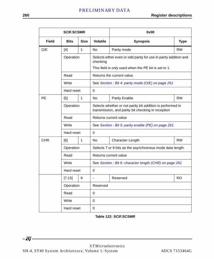
260 Register descriptionsPRELIMINARY DATA
O/E [4] 1 No Parity mode RW
Operation Selects either even or odd parity for use in parity addition and checking
This field is only used when the PE bit is set to 1.
Read Returns the current value.
Write See Section : Bit 4: parity mode (O/E) on page 261
Hard reset 0
PE [5] 1 No Parity Enable RW
Operation Selects whether or not parity bit addition is performed in transmission, and parity bit checking in reception
Read Returns current value
Write See Section : Bit 5: parity enable (PE) on page 261
Hard reset 0
CHR [6] 1 No Character Length RW
Operation Selects 7 or 8 bits as the asynchronous mode data length.
Read Returns current value
Write See Section : Bit 6: character length (CHR) on page 261
Hard reset 0
[7:15] 9 - Reserved RO
Operation Reserved
Read 0
Write 0
Hard reset 0
SCIF.SCSMR 0x00
Field Bits Size Volatile Synopsis Type
Table 122: SCIF.SCSMR
STMicroelectronicsSH-4, ST40 System Architecture, Volume 1: System ADCS 7153464G
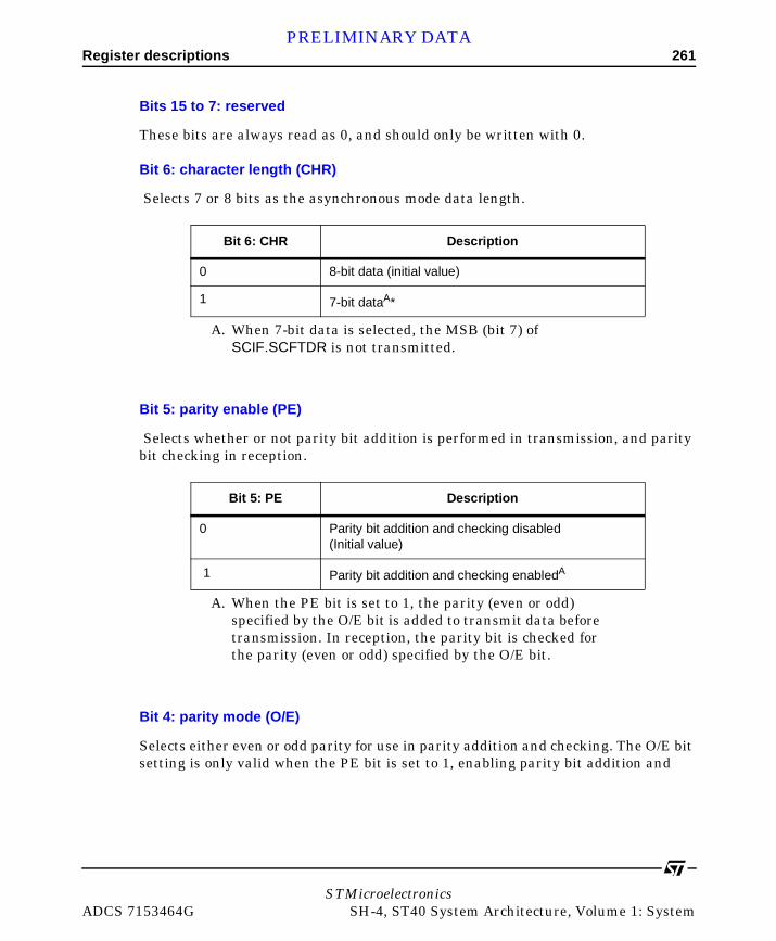
Register descriptions 261PRELIMINARY DATA
Bits 15 to 7: reserved
These bits are always read as 0, and should only be written with 0.
Bit 6: character length (CHR)
Selects 7 or 8 bits as the asynchronous mode data length.
Bit 5: parity enable (PE)
Selects whether or not parity bit addition is performed in transmission, and parity bit checking in reception.
Bit 4: parity mode (O/E)
Selects either even or odd parity for use in parity addition and checking. The O/E bit setting is only valid when the PE bit is set to 1, enabling parity bit addition and
Bit 6: CHR Description
0 8-bit data (initial value)
1 7-bit dataA*
A. When 7-bit data is selected, the MSB (bit 7) of SCIF.SCFTDR is not transmitted.
Bit 5: PE Description
0 Parity bit addition and checking disabled (Initial value)
1 Parity bit addition and checking enabledA
A. When the PE bit is set to 1, the parity (even or odd) specified by the O/E bit is added to transmit data before transmission. In reception, the parity bit is checked for the parity (even or odd) specified by the O/E bit.
STMicroelectronicsADCS 7153464G SH-4, ST40 System Architecture, Volume 1: System

262 Register descriptionsPRELIMINARY DATA
checking. The O/E bit setting is invalid when parity addition and checking is disabled.
Bit 3: stop bit length (STOP)
Selects 1 or 2 bits as the stop bit length.
Bit 4: O/E Description
0 Even parityA (initial value)
A. When even parity is set, parity bit addition is performed in transmission so that the total number of 1 bits in the transmit character plus the parity bit is even. In reception, a check is performed to see if the total number of 1 bits in the receive character plus the parity bit is even.
1 Odd parityB
B. When odd parity is set, parity bit addition is performed in transmission so that the total number of 1 bits in the transmit character plus the parity bit is odd. In reception, a check is performed to see if the total number of 1 bits in the receive character plus the parity bit is odd.
Bit 3: STOP Description
0 1 stop bitA (initial value)
A. In transmission, 1 bit (stop bit) is added to the end of a transmit character before it is sent.
1 2 stop bitsB
B. In transmission, 2 bits (stop bits) are added to the end of a transmit character before it is sent.
STMicroelectronicsSH-4, ST40 System Architecture, Volume 1: System ADCS 7153464G

Register descriptions 263PRELIMINARY DATA
In reception, only the first stop bit is checked, regardless of the stop bit setting. If the second stop bit is 1, it is treated as a stop bit; if it is 0, it is treated as the start bit of the next transmit character.
Bit 2: reserved
This bit is always read as 0, and should only be written with 0.
Bits 1 and 0: clock select 1 and 0 (CKS1, CKS0)
These bits select the clock source for the on-chip baud rate generator. The clock source can be selected from Pø, Pø/4, Pø/16, and Pø/64, according to the setting of bits CKS1 and CKS0. For the relation between the clock source, the bit rate register setting, and the baud rate, see Section 9.2.8: Bit rate register (SCIF.SCBRR) on page 282.
Bit 1: CKS1 Bit 0: CKS0 Description
0 0 PφA clock (initial value)
A. Pø: Peripheral clock
1 Pφ/4 clock
1 0 Pφ/16 clock
1 Pφ/64 clock
STMicroelectronicsADCS 7153464G SH-4, ST40 System Architecture, Volume 1: System
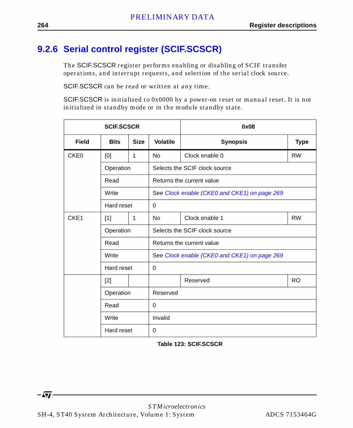
264 Register descriptionsPRELIMINARY DATA
9.2.6 Serial control register (SCIF.SCSCR)
The SCIF.SCSCR register performs enabling or disabling of SCIF transfer operations, and interrupt requests, and selection of the serial clock source.
SCIF.SCSCR can be read or written at any time.
SCIF.SCSCR is initialized to 0x0000 by a power-on reset or manual reset. It is not initialized in standby mode or in the module standby state.
SCIF.SCSCR 0x08
Field Bits Size Volatile Synopsis Type
CKE0 [0] 1 No Clock enable 0 RW
Operation Selects the SCIF clock source
Read Returns the current value
Write See Clock enable (CKE0 and CKE1) on page 269
Hard reset 0
CKE1 [1] 1 No Clock enable 1 RW
Operation Selects the SCIF clock source
Read Returns the current value
Write See Clock enable (CKE0 and CKE1) on page 269
Hard reset 0
[2] Reserved RO
Operation Reserved
Read 0
Write Invalid
Hard reset 0
Table 123: SCIF.SCSCR
STMicroelectronicsSH-4, ST40 System Architecture, Volume 1: System ADCS 7153464G

Register descriptions 265PRELIMINARY DATA
REIE [3] 1 No Receive error interrupt enable RW
Operation Enables or disables generation of receive-error interrupt (ERI) and BREAK interrupt (BRI) requests
Read Returns the current value
Write See Bit 3: receive error interrupt enable (REIE) on page 269.
Hard reset 0
RE [4] 1 No Receive enable RW
Operation Enables or disables the start of serial reception by the SCIF
Read Returns the current value
Write See Bit 4: receive enable (RE) on page 268
Hard reset 0
TE [5] 1 No Transmit enable RW
Operation Enables or disables the start of serial transmission by the SCIF
Read Returns the current value
Write See Bit 5: transmit enable (TE) on page 268.
Hard reset 0
RIE [6] 1 No Receive interrupt enable RW
Operation Enables or disables generation of a receive interrupts
Read Returns the current value
Write See Bit 6: receive interrupt enable (RIE) on page 267
Hard reset 0
SCIF.SCSCR 0x08
Field Bits Size Volatile Synopsis Type
Table 123: SCIF.SCSCR
STMicroelectronicsADCS 7153464G SH-4, ST40 System Architecture, Volume 1: System

266 Register descriptionsPRELIMINARY DATA
Bits 15 to 8 and 2: reserved
These bits are always read as 0, and should only be written with 0.
TIE [7] 1 No Transmit interrupt enable RW
Operation Enables or disables transmit interrupts
Read Returns the current value
Write See Bit 7: transmit interrupt enable (TIE) on page 267
Hard reset 0
[8:15] No Reserved RO
Operation Reserved
Read 0
Write Invalid
Hard reset 0
SCIF.SCSCR 0x08
Field Bits Size Volatile Synopsis Type
Table 123: SCIF.SCSCR
STMicroelectronicsSH-4, ST40 System Architecture, Volume 1: System ADCS 7153464G

Register descriptions 267PRELIMINARY DATA
Bit 7: transmit interrupt enable (TIE)
Bit 7 enables or disables TRANSMIT-FIFO-DATA-EMPTY interrupt (TXI) request generation when serial transmit data is transferred from SCIF.SCFTDR to SCIF.SCTSR. The number of data bytes in the transmit FIFO register falls to or below the transmit trigger set number, and the TDFE flag in the serial status register (SCIF.SCFSR) is set to 1.
Bit 6: receive interrupt enable (RIE)
Bit 6 enables or disables generation of the following requests:
• a receive data full interrupt (RXI) request when the RDF flag or DR flag in SCIF.SCFSR is set to 1,
• a receive error interrupt (ERI) request when the ER flag in SCIF.SCFSR is set to 1,
• a BREAK interrupt (BRI) request when the BRK flag in SCIF.SCFSR or the ORER flag in SCIF.SCLSR is set to 1.
Bit 7: TIE Description
0 TRANSMIT-FIFO-DATA-EMPTY interrupt (TXI)
request disabledA
(initial value)
A. TXI interrupt requests can be cleared by writing transmit data exceeding the transmit trigger set number to SCIF.SCFTDR, reading 1 from the TDFE flag, then clearing it to 0, or by clearing the TIE bit to 0.
1 Transmit-FIFO-data-empty interrupt (TXI) request enabled
Bit 6: RIE Description
0 Disables the RXI, ERI and BRI requests (initial
value)A
1 Enables the RXI, ERI and BRI requests
STMicroelectronicsADCS 7153464G SH-4, ST40 System Architecture, Volume 1: System

268 Register descriptionsPRELIMINARY DATA
Bit 5: transmit enable (TE)
Bit 5 enables or disables the start of serial transmission by the SCIF.
Bit 4: receive enable (RE)
Bit 4 enables or disables the start of serial reception by the SCIF.
A. An RXI interrupt request can be cleared by reading 1 from the RDF or DR flag, then clearing the flag to 0, or by clearing the RIE bit to 0. ERI and BRI interrupt requests can be cleared by reading 1 from the ER, BRK, or ORER flag, then clearing the flag to 0, or by clearing the RIE and REIE bits to 0.
Bit 5: TE Description
0 Transmission disabled (initial value)
1 Transmission enabledA
A. Serial transmission is started when transmit data is written to SCIF.SCFTDR in this state.
Serial mode register (SCIF.SCSMR) and FIFO control register (SCIF.SCFCR) settings must be made, the transmission format decided, and the transmit FIFO reset, before the TE bit is set to 1.
Bit 4: RE Description
0 Reception disabledA (initial value)
A. Clearing the RE bit to 0 does not affect the DR, ER, BRK, RDF, FER, PER, and ORER flags, which retain their states.
1 Reception enabledB
STMicroelectronicsSH-4, ST40 System Architecture, Volume 1: System ADCS 7153464G

Register descriptions 269PRELIMINARY DATA
Bit 3: receive error interrupt enable (REIE)
Bit 3 enables or disables generation of receive error interrupt (ERI) and BREAK interrupt (BRI) requests. The REIE bit setting is valid only when the RIE bit is 0.
Bit 2: reserved
This bit is always read as 0, and cannot be modified.
Clock enable (CKE0 and CKE1)
These bits select the SCIF clock source and enable or disable clock output from the SCK pin. The combination of CKE1 and CKE0 determine whether the SCK pin functions as serial clock output pin or the serial clock input pin.
B. Serial transmission is started when a start bit is detected in this state. Serial mode register (SCIF.SCSMR) and FIFO control register (SCIF.SCFCR) settings must be made, the reception format decided, and the receive FIFO reset, before the RE bit is set to 1.
Bit 3: REIE Description
0 ERI and BRI requests disabledA (initial value)
A. ERI and BRI requests can be cleared by reading 1 from the ER, BRK, or ORER flag, then clearing the flag to 0, or by clearing the RIE and REIE bits to 0. When REIE is set to 1, ERI and BRI requests are generated even if RIE is cleared to 0. In DMAC transfer, this setting is made if the interrupt controller is to be notified of ERI and BRI requests.
1 ERI and BRI requests enabled
STMicroelectronicsADCS 7153464G SH-4, ST40 System Architecture, Volume 1: System

270 Register descriptionsPRELIMINARY DATA
Note: however, the setting of the CKE0 bit is valid only when CKE1: 0 (internal clock operation). When CKE1: 1 (external clock) CKE0 is ignored. These bits must be set before determining the SCIF’s operating mode with SCIF.SCSMR.
9.2.7 Serial status register (SCIF.SCFSR)
SCIF.SCFSR is a 16-bit register. The lower 8 bits consist of status flags that indicate the operating status of the SCIF, and the upper 8 bits indicate the number of receive errors in the data in the receive FIFO register.
SCIF.SCFSR can be read or written to by the CPU at all times. However, 1 cannot be written to flags ER, TEND, TDFE, BRK, RDF, and DR.
Note: in order to clear these flags they must be read as 1 beforehand. The FER flag and PER flag are read-only flags and cannot be modified.
SCIF.SCFSR is initialized to 0x0060 by a power-on reset or manual reset. It is not initialized in standby mode or in the module standby state.
Bit 1: CKE1 Bit 0: CKE0 Description
0 0 Use internal clock
SCK pin functions as input pin, input signal ignored (initial value)
0 1 Use internal clock
SCK pin functions as clock outputA
A. Outputs a clock with a frequency 16 times the bit rate.
STMicroelectronicsSH-4, ST40 System Architecture, Volume 1: System ADCS 7153464G
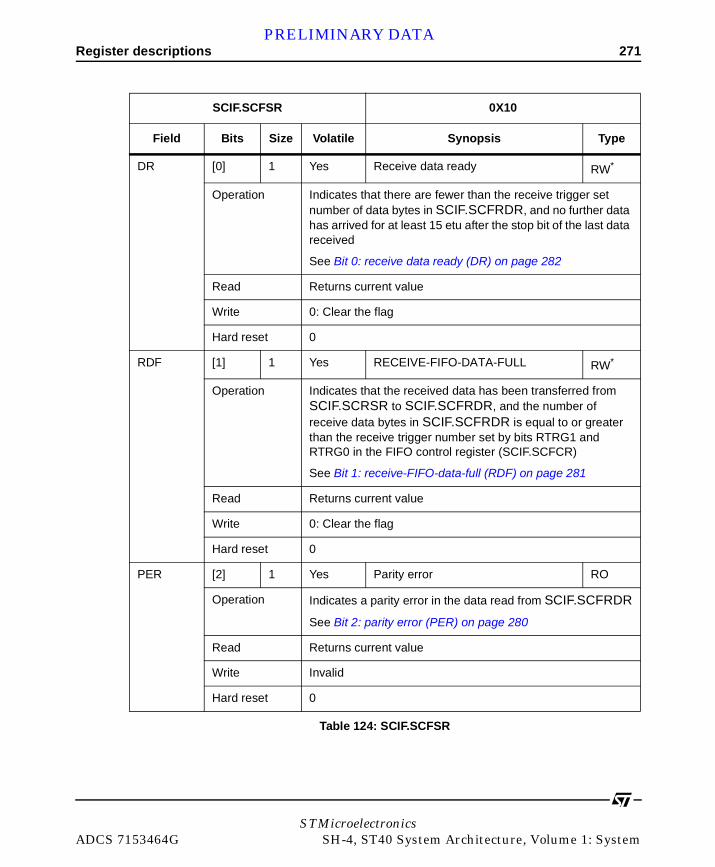
Register descriptions 271PRELIMINARY DATA
SCIF.SCFSR 0X10
Field Bits Size Volatile Synopsis Type
DR [0] 1 Yes Receive data ready RW*
Operation Indicates that there are fewer than the receive trigger set number of data bytes in SCIF.SCFRDR, and no further data has arrived for at least 15 etu after the stop bit of the last data received
See Bit 0: receive data ready (DR) on page 282
Read Returns current value
Write 0: Clear the flag
Hard reset 0
RDF [1] 1 Yes RECEIVE-FIFO-DATA-FULL RW*
Operation Indicates that the received data has been transferred from SCIF.SCRSR to SCIF.SCFRDR, and the number of receive data bytes in SCIF.SCFRDR is equal to or greater than the receive trigger number set by bits RTRG1 and RTRG0 in the FIFO control register (SCIF.SCFCR)
See Bit 1: receive-FIFO-data-full (RDF) on page 281
Read Returns current value
Write 0: Clear the flag
Hard reset 0
PER [2] 1 Yes Parity error RO
Operation Indicates a parity error in the data read from SCIF.SCFRDR
See Bit 2: parity error (PER) on page 280
Read Returns current value
Write Invalid
Hard reset 0
Table 124: SCIF.SCFSR
STMicroelectronicsADCS 7153464G SH-4, ST40 System Architecture, Volume 1: System
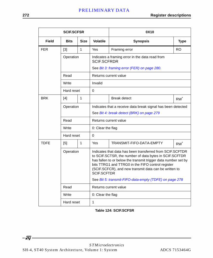
272 Register descriptionsPRELIMINARY DATA
FER [3] 1 Yes Framing error RO
Operation Indicates a framing error in the data read from SCIF.SCFRDR
See Bit 3: framing error (FER) on page 280.
Read Returns current value
Write Invalid
Hard reset 0
BRK [4] 1 Break detect RW*
Operation Indicates that a receive data break signal has been detected
See Bit 4: break detect (BRK) on page 279
Read Returns current value
Write 0: Clear the flag
Hard reset 0
TDFE [5] 1 Yes TRANSMIT-FIFO-DATA-EMPTY RW*
Operation Indicates that data has been transferred from SCIF.SCFTDR to SCIF.SCTSR, the number of data bytes in SCIF.SCFTDR has fallen to or below the transmit trigger data number set by bits TTRG1 and TTRG0 in the FIFO control register (SCIF.SCFCR), and new transmit data can be written to SCIF.SCFTDR
See Bit 5: transmit-FIFO-data-empty (TDFE) on page 278
Read Returns current value
Write 0: Clear the flag
Hard reset 1
SCIF.SCFSR 0X10
Field Bits Size Volatile Synopsis Type
Table 124: SCIF.SCFSR
STMicroelectronicsSH-4, ST40 System Architecture, Volume 1: System ADCS 7153464G

Register descriptions 273PRELIMINARY DATA
TEND [6] 1 Yes Transmit end RW*
Operation Indicates that there is no valid data in SCIF.SCFTDR when the last bit of the transmit character is sent, and transmission has been ended
See Bit 6: transmit end (TEND) on page 277.
Read Returns current value
Write 0: Clear the flag
Hard reset 1
ER [7] 1 Receive error RW*
Operation Indicates that a framing error or parity error occurred during reception.See Bit 7: receive error (ER) on page 274.
Read Returns current value
Write *Only 0 can be written. This clears the flag
Hard reset 0
FER3 to FER0
[8:11] 4 Yes Number of framing errors RO
Operation These bits indicate the number of data bytes in which a framing error occurred in the receive data stored in SCIF.SCFRDR
See Bits 11 to 8: number of framing errors (FER3 to FER0) on page 274
Read Returns current value
Write Invalid
Hard reset 0
SCIF.SCFSR 0X10
Field Bits Size Volatile Synopsis Type
Table 124: SCIF.SCFSR
STMicroelectronicsADCS 7153464G SH-4, ST40 System Architecture, Volume 1: System

274 Register descriptionsPRELIMINARY DATA
Bits 15 to 12: number of parity errors (PER3 to PER0)
Bits 15 to 12 indicate the number of data bytes in which a parity error occurred in the receive data stored in SCIF.SCFRDR. After the ER bit in SCIF.SCFSR is set, the value indicated by bits 15 to 12 is the number of data bytes in which a parity error occurred. If all 16 bytes of receive data in SCIF.SCFRDR have parity errors, the value indicated by bits PER3 to PER0 will be 0.
Bits 11 to 8: number of framing errors (FER3 to FER0)
Bits 11 to 8 indicate the number of data bytes in which a framing error occurred in the receive data stored in SCIF.SCFRDR. After the ER bit in SCIF.SCFSR is set, the value indicated by bits 11 to 8 is the number of data bytes in which a framing error occurred. If all 16 bytes of receive data in SCIF.SCFRDR have framing errors, the value indicated by bits FER3 to FER0 will be 0.
Bit 7: receive error (ER)
Bit 7 indicates that a framing error or parity error occurred during reception. The ER flag is not affected and retains its previous state when the RE bit in SCIF.SCSCR is cleared to 0. When a receive error occurs, the receive data is still transferred to SCIF.SCFRDR, and reception continues. The FER and PER bits in SCIF.SCFSR can be used to determine whether there is a receive error in the data read from SCIF.SCFRDR.
PER3 toPER0
[12:15] 4 Yes Number of parity errors RO
Operation These bits indicate the number of data bytes in which a parity error occurred in the receive data stored in SCIF.SCFRDR
See Bits 15 to 12: number of parity errors (PER3 to PER0) on page 274.
Read Returns current value
Write Invalid
Hard reset 0
SCIF.SCFSR 0X10
Field Bits Size Volatile Synopsis Type
Table 124: SCIF.SCFSR
STMicroelectronicsSH-4, ST40 System Architecture, Volume 1: System ADCS 7153464G

Register descriptions 275PRELIMINARY DATA
.
STMicroelectronicsADCS 7153464G SH-4, ST40 System Architecture, Volume 1: System

276 Register descriptionsPRELIMINARY DATA
Bit 7: ER Description
0 No framing error or parity error occurred during reception (initial value)
Clearing conditions are:
Power-on reset
Manual reset
When 0 is written to ER after reading ER = 1
1 A framing error or parity error occurred during reception
Setting conditions are:
When the SCIF checks whether the stop bit at the end of the receive data is 1
When reception ends, and the stop bit is 0A
When, in reception, the number of 1 bits in the receive data plus the parity bit does not match the parity setting (even or odd) specified by the O/E bit in SCIF.SCSMR
A. In 2 stop bit mode, only the first stop bit is checked for a value of 1. The second stop bit is not checked.
STMicroelectronicsSH-4, ST40 System Architecture, Volume 1: System ADCS 7153464G

Register descriptions 277PRELIMINARY DATA
Bit 6: transmit end (TEND)
Bit 6 indicates that there is no valid data in SCIF.SCFTDR when the last bit of the transmit character is sent, and transmission has been ended.
Bit 6: TEND Description
0 Transmission in progress
Clearing conditions are:
When transmit data is written to SCIF.SCFTDR, and 0 is written to TEND after reading TEND = 1.
When data is written to SCIF.SCFTDR by the DMAC
1 Transmission ended (initial value)
Setting conditions are:
When there is a power-on reset or manual reset.
When the TE bit in SCIF.SCSCR is 0.
When there is no transmit data in SCIF.SCFTDR on transmission of the last bit of a 1-byte serial transmit character.
STMicroelectronicsADCS 7153464G SH-4, ST40 System Architecture, Volume 1: System
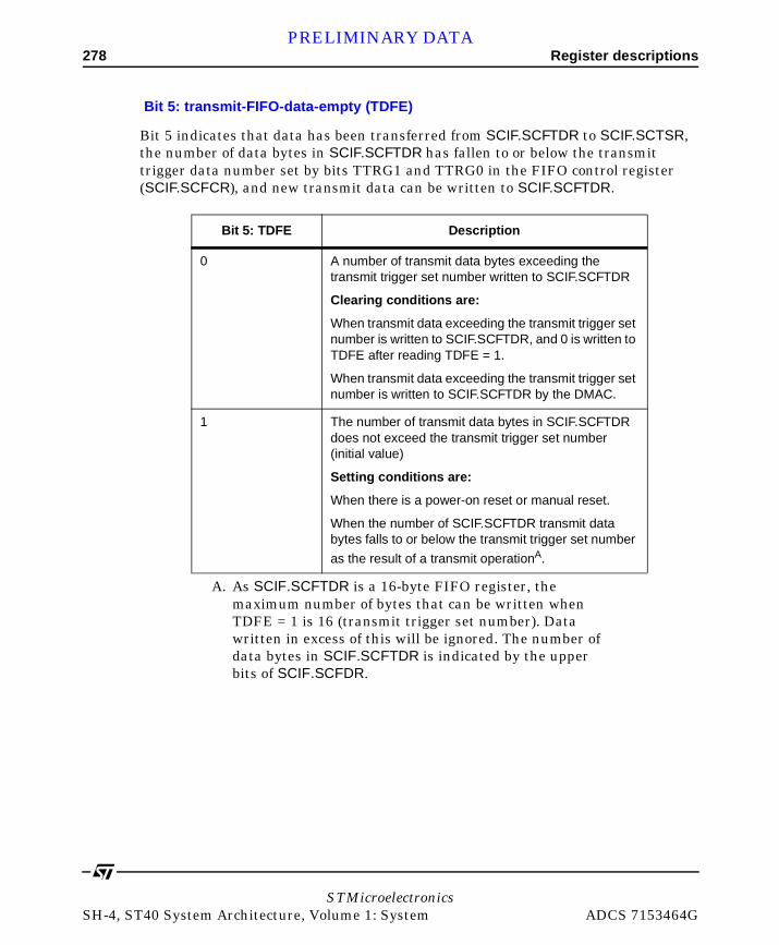
278 Register descriptionsPRELIMINARY DATA
Bit 5: transmit-FIFO-data-empty (TDFE)
Bit 5 indicates that data has been transferred from SCIF.SCFTDR to SCIF.SCTSR, the number of data bytes in SCIF.SCFTDR has fallen to or below the transmit trigger data number set by bits TTRG1 and TTRG0 in the FIFO control register (SCIF.SCFCR), and new transmit data can be written to SCIF.SCFTDR.
Bit 5: TDFE Description
0 A number of transmit data bytes exceeding the transmit trigger set number written to SCIF.SCFTDR
Clearing conditions are:
When transmit data exceeding the transmit trigger set number is written to SCIF.SCFTDR, and 0 is written to TDFE after reading TDFE = 1.
When transmit data exceeding the transmit trigger set number is written to SCIF.SCFTDR by the DMAC.
1 The number of transmit data bytes in SCIF.SCFTDR does not exceed the transmit trigger set number (initial value)
Setting conditions are:
When there is a power-on reset or manual reset.
When the number of SCIF.SCFTDR transmit data bytes falls to or below the transmit trigger set number
as the result of a transmit operationA.
A. As SCIF.SCFTDR is a 16-byte FIFO register, the maximum number of bytes that can be written when TDFE = 1 is 16 (transmit trigger set number). Data written in excess of this will be ignored. The number of data bytes in SCIF.SCFTDR is indicated by the upper bits of SCIF.SCFDR.
STMicroelectronicsSH-4, ST40 System Architecture, Volume 1: System ADCS 7153464G
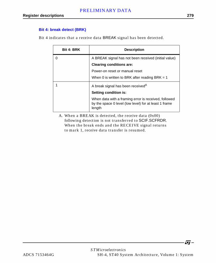
Register descriptions 279PRELIMINARY DATA
Bit 4: break detect (BRK)
Bit 4 indicates that a receive data BREAK signal has been detected.
Bit 4: BRK Description
0 A BREAK signal has not been received (initial value)
Clearing conditions are:
Power-on reset or manual reset
When 0 is written to BRK after reading BRK = 1
1 A break signal has been receivedA
Setting condition is:
When data with a framing error is received, followed by the space 0 level (low level) for at least 1 frame length
A. When a BREAK is detected, the receive data (0x00) following detection is not transferred to SCIF.SCFRDR. When the break ends and the RECEIVE signal returns to mark 1, receive data transfer is resumed.
STMicroelectronicsADCS 7153464G SH-4, ST40 System Architecture, Volume 1: System
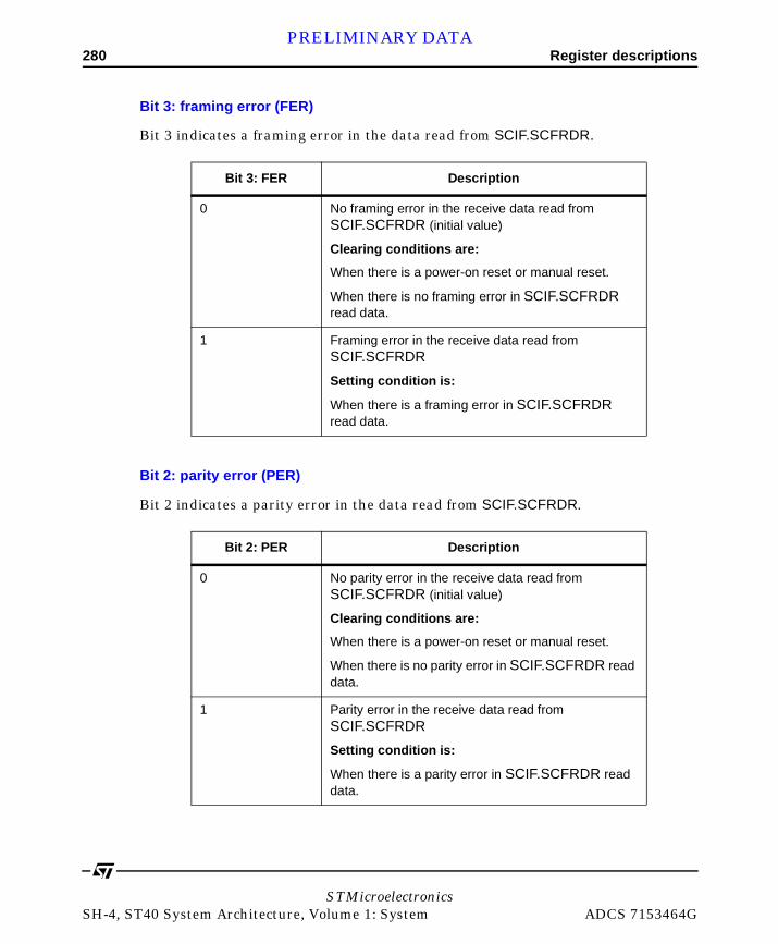
280 Register descriptionsPRELIMINARY DATA
Bit 3: framing error (FER)
Bit 3 indicates a framing error in the data read from SCIF.SCFRDR.
Bit 2: parity error (PER)
Bit 2 indicates a parity error in the data read from SCIF.SCFRDR.
Bit 3: FER Description
0 No framing error in the receive data read from SCIF.SCFRDR (initial value)
Clearing conditions are:
When there is a power-on reset or manual reset.
When there is no framing error in SCIF.SCFRDR read data.
1 Framing error in the receive data read from SCIF.SCFRDR
Setting condition is:
When there is a framing error in SCIF.SCFRDR read data.
Bit 2: PER Description
0 No parity error in the receive data read from SCIF.SCFRDR (initial value)
Clearing conditions are:
When there is a power-on reset or manual reset.
When there is no parity error in SCIF.SCFRDR read data.
1 Parity error in the receive data read from SCIF.SCFRDR
Setting condition is:
When there is a parity error in SCIF.SCFRDR read data.
STMicroelectronicsSH-4, ST40 System Architecture, Volume 1: System ADCS 7153464G
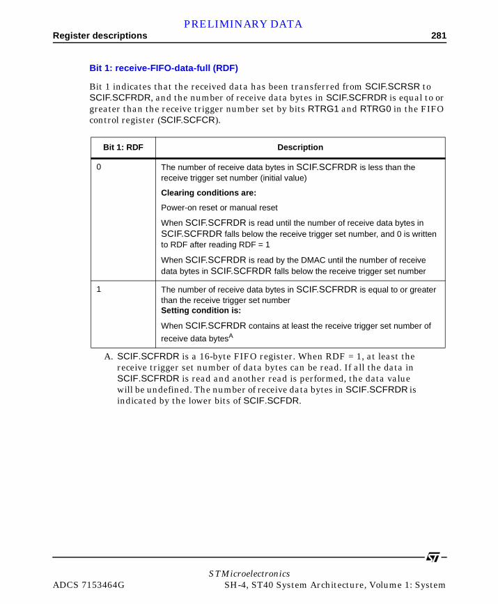
Register descriptions 281PRELIMINARY DATA
Bit 1: receive-FIFO-data-full (RDF)
Bit 1 indicates that the received data has been transferred from SCIF.SCRSR to SCIF.SCFRDR, and the number of receive data bytes in SCIF.SCFRDR is equal to or greater than the receive trigger number set by bits RTRG1 and RTRG0 in the FIFO control register (SCIF.SCFCR).
Bit 1: RDF Description
0 The number of receive data bytes in SCIF.SCFRDR is less than the receive trigger set number (initial value)
Clearing conditions are:
Power-on reset or manual reset
When SCIF.SCFRDR is read until the number of receive data bytes in SCIF.SCFRDR falls below the receive trigger set number, and 0 is written to RDF after reading RDF = 1
When SCIF.SCFRDR is read by the DMAC until the number of receive data bytes in SCIF.SCFRDR falls below the receive trigger set number
1 The number of receive data bytes in SCIF.SCFRDR is equal to or greater than the receive trigger set numberSetting condition is:
When SCIF.SCFRDR contains at least the receive trigger set number of
receive data bytesA
A. SCIF.SCFRDR is a 16-byte FIFO register. When RDF = 1, at least the receive trigger set number of data bytes can be read. If all the data in SCIF.SCFRDR is read and another read is performed, the data value will be undefined. The number of receive data bytes in SCIF.SCFRDR is indicated by the lower bits of SCIF.SCFDR.
STMicroelectronicsADCS 7153464G SH-4, ST40 System Architecture, Volume 1: System
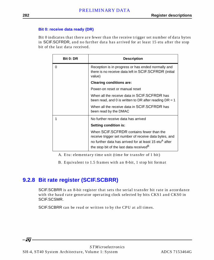
282 Register descriptionsPRELIMINARY DATA
Bit 0: receive data ready (DR)
Bit 0 indicates that there are fewer than the receive trigger set number of data bytes in SCIF.SCFRDR, and no further data has arrived for at least 15 etu after the stop bit of the last data received.
9.2.8 Bit rate register (SCIF.SCBRR)
SCIF.SCBRR is an 8-bit register that sets the serial transfer bit rate in accordance with the baud rate generator operating clock selected by bits CKS1 and CKS0 in SCIF.SCSMR.
SCIF.SCBRR can be read or written to by the CPU at all times.
Bit 0: DR Description
0 Reception is in progress or has ended normally and there is no receive data left in SCIF.SCFRDR (initial value)
Clearing conditions are:
Power-on reset or manual reset
When all the receive data in SCIF.SCFRDR has been read, and 0 is written to DR after reading DR = 1
When all the receive data in SCIF.SCFRDR has been read by the DMAC
1 No further receive data has arrived
Setting condition is:
When SCIF.SCFRDR contains fewer than the receive trigger set number of receive data bytes, and
no further data has arrived for at least 15 etuA after
the stop bit of the last data receivedB
A. Etu: elementary time unit (time for transfer of 1 bit)
B. Equivalent to 1.5 frames with an 8-bit, 1 stop bit format
STMicroelectronicsSH-4, ST40 System Architecture, Volume 1: System ADCS 7153464G

Register descriptions 283PRELIMINARY DATA
SCIF.SCBRR is initialized to H’FF by a power-on reset or manual reset. It is not initialized in standby mode or in the module standby state.
The SCIF.SCBRR setting is found from the following equation. Asynchronous mode
Where:
B = Bit rate (bits/s)
N =SCIF.SCBRR setting for baud rate generator (0 ≤ N ≤ 255)
Pφ = Peripheral module operating frequency (MHz)
n = Baud rate generator input clock (n = 0 to 3)
(See Table 126 for the relation between n and the clock.)
SCIF.SCBRR 0x04
Field Bits Size Volatile Synopsis Type
SCBRR [0:7] 8 Bit rate register RW
Operation Specifies the serial transfer bit rate in accordance with the baud rate generator operating clock
Read Returns current value
Write Updates current Value
Hard reset 0xFF
Table 125: SCIF.SCBRR
Pφ
64 22n 1–
B××------------------------------------- 10
61–× N=
STMicroelectronicsADCS 7153464G SH-4, ST40 System Architecture, Volume 1: System
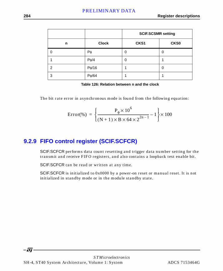
284 Register descriptionsPRELIMINARY DATA
The bit rate error in asynchronous mode is found from the following equation:
9.2.9 FIFO control register (SCIF.SCFCR)
SCIF.SCFCR performs data count resetting and trigger data number setting for the transmit and receive FIFO registers, and also contains a loopback test enable bit.
SCIF.SCFCR can be read or written at any time.
SCIF.SCFCR is initialized to 0x0000 by a power-on reset or manual reset. It is not initialized in standby mode or in the module standby state.
SCIF.SCSMR setting
n Clock CKS1 CKS0
0 Pφ 0 0
1 Pφ/4 0 1
2 Pφ/16 1 0
3 Pφ/64 1 1
Table 126: Relation between n and the clock
Error %( )Pφ 10
6×
N 1+( ) B× 64× 22n 1–×
-------------------------------------------------------------- 1–
100×=
STMicroelectronicsSH-4, ST40 System Architecture, Volume 1: System ADCS 7153464G
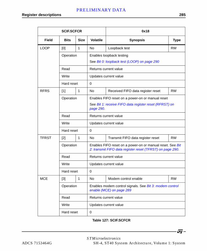
Register descriptions 285PRELIMINARY DATA
SCIF.SCFCR 0x18
Field Bits Size Volatile Synopsis Type
LOOP [0] 1 No Loopback test RW
Operation Enables loopback testing
See Bit 0: loopback test (LOOP) on page 290
Read Returns current value
Write Updates current value
Hard reset 0
RFRS [1] 1 No Received FIFO data register reset RW
Operation Enables FIFO reset on a power-on or manual reset
See Bit 1: receive FIFO data register reset (RFRST) on page 290.
Read Returns current value
Write Updates current value
Hard reset 0
TFRST [2] 1 No Transmit FIFO data register reset RW
Operation Enables FIFO reset on a power-on or manual reset. See Bit 2: transmit FIFO data register reset (TFRST) on page 290.
Read Returns current value
Write Updates current value
Hard reset 0
MCE [3] 1 No Modem control enable RW
Operation Enables modem control signals. See Bit 3: modem control enable (MCE) on page 289
Read Returns current value
Write Updates current value
Hard reset 0
Table 127: SCIF.SCFCR
STMicroelectronicsADCS 7153464G SH-4, ST40 System Architecture, Volume 1: System
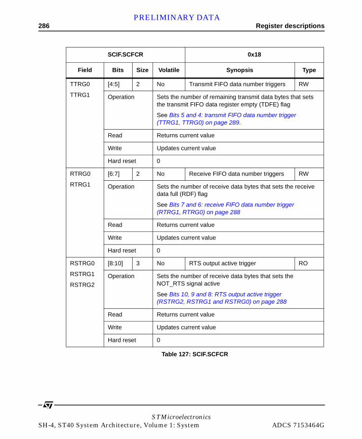
286 Register descriptionsPRELIMINARY DATA
TTRG0
TTRG1
[4:5] 2 No Transmit FIFO data number triggers RW
Operation Sets the number of remaining transmit data bytes that sets the transmit FIFO data register empty (TDFE) flag
See Bits 5 and 4: transmit FIFO data number trigger (TTRG1, TTRG0) on page 289.
Read Returns current value
Write Updates current value
Hard reset 0
RTRG0
RTRG1
[6:7] 2 No Receive FIFO data number triggers RW
Operation Sets the number of receive data bytes that sets the receive data full (RDF) flag
See Bits 7 and 6: receive FIFO data number trigger (RTRG1, RTRG0) on page 288
Read Returns current value
Write Updates current value
Hard reset 0
RSTRG0
RSTRG1
RSTRG2
[8:10] 3 No RTS output active trigger RO
Operation Sets the number of receive data bytes that sets the NOT_RTS signal active
See Bits 10, 9 and 8: RTS output active trigger (RSTRG2, RSTRG1 and RSTRG0) on page 288
Read Returns current value
Write Updates current value
Hard reset 0
SCIF.SCFCR 0x18
Field Bits Size Volatile Synopsis Type
Table 127: SCIF.SCFCR
STMicroelectronicsSH-4, ST40 System Architecture, Volume 1: System ADCS 7153464G

Register descriptions 287PRELIMINARY DATA
Bits 15 to 11: reserved
Bits 15 to 11 are always read as 0, and should only be written with 0.
[11:15] 5 Yes Reserved RO
Operation Reserved.
Read 0
Write 0 (should only be written with 0)
Hard reset 0
SCIF.SCFCR 0x18
Field Bits Size Volatile Synopsis Type
Table 127: SCIF.SCFCR
STMicroelectronicsADCS 7153464G SH-4, ST40 System Architecture, Volume 1: System

288 Register descriptionsPRELIMINARY DATA
Bits 10, 9 and 8: RTS output active trigger (RSTRG2, RSTRG1 and RSTRG0)
Bits 10, 9 and 8 set the NOT_RTS signal active when the number of received data stored in the receive FIFO data register (SCFRDR) exceeds the trigger number, as shown in the table.
Bits 7 and 6: receive FIFO data number trigger (RTRG1, RTRG0)
Bits 7 and 6 are used to set the number of receive data bytes that sets the receive data full (RDF) flag in the serial status register (SCIF.SCFSR).
The RDF flag is set when the number of receive data bytes in SCIF.SCFRDR is equal to or greater than the trigger set number shown in the following table.
Bit 10: RSTRG2 Bit 9: RSTRG1 Bit 8: RSTRG0RTS output
active trigger
0 0 0 15 (initial value)
0 0 1 1
0 1 0 4
0 1 1 6
1 0 0 8
1 0 1 10
1 1 0 12
1 1 1 14
Bit 7: RTRG1 Bit 6: RTRG0Receive trigger
number
0 0 1 (initial value)
1 4
1 0 8
1 14
STMicroelectronicsSH-4, ST40 System Architecture, Volume 1: System ADCS 7153464G

Register descriptions 289PRELIMINARY DATA
Bits 5 and 4: transmit FIFO data number trigger (TTRG1, TTRG0)
Bits 5 and 4 are used to set the number of remaining transmit data bytes that sets the transmit FIFO data register empty (TDFE) flag in the serial status register (SCIF.SCFSR). The TDFE flag is set when the number of transmit data bytes in SCIF.SCFTDR is equal to or less than the trigger set number shown in the following table.
Bit 3: modem control enable (MCE)
Bit 3 enables the CTS and RTS modem control signals.
Bit 5: TTRG1 Bit 4: TTRG0Transmit trigger
number
Empty bytes in SCIF.SCFTDR
when TDFE flag is set
0 0 8 8
1 4 12
1 0 2 14
1 1 15
Bit 3: MCE Description
0 Modem signals disabledA (initial value)
A. CTS is fixed at active 0 regardless of the input value, and RTS output is also fixed at 0.
1 Modem signals enabled
STMicroelectronicsADCS 7153464G SH-4, ST40 System Architecture, Volume 1: System

290 Register descriptionsPRELIMINARY DATA
Bit 2: transmit FIFO data register reset (TFRST)
Bit 2 invalidates the transmit data in the transmit FIFO data register and resets it to the empty state.
Bit 1: receive FIFO data register reset (RFRST)
Bit 1 invalidates the receive data in the receive FIFO data register and resets it to the empty state. A reset operation is performed in the event of a power-on reset or manual reset.
Bit 0: loopback test (LOOP)
Bit 0 internally connects the transmit output pin (TXD) and receive input pin (RXD), and the RTS pin and CTS pin, enabling loopback testing.
Bit 2: TFRST
Description
0 Reset operation disabledA (initial value)
A. A reset operation is performed in the event of a power-on reset or manual reset.
1 Reset operation enabled
Bit 1: RFRST Description
0 Reset operation disabled (initial value)
1 Reset operation enabled
Bit 0: LOOP Description
0 Loopback test disabled (initial value)
1 Loopback test enabled
STMicroelectronicsSH-4, ST40 System Architecture, Volume 1: System ADCS 7153464G

Register descriptions 291PRELIMINARY DATA
9.2.10 FIFO data count register (SCIF.SCFDR)
SCIF.SCFDR is a 16-bit register that indicates the number of data bytes stored in SCIF.SCFTDR and SCIF.SCFRDR.
The upper bits show the number of transmit data bytes in SCIF.SCFTDR, and the lower bits show the number of receive data bytes in SCIF.SCFRDR.
SCIF.SCFDR can be read by the CPU at all times.
SCIF.SCFDR 0x1C
Field Bits Size Volatile Synopsis Type
R0
R1
R2
R3
R4
[0:4] 8 Yes Received data count RO
Operation These bits show the number of receive data bytes in SCIF.SCFRDR
Read Returns the current count
A value of 0x00 indicates that there is no receive data, and a value of 0x10 indicates that SCIF.SCFRDR is full of receive data.
Write Invalid
Hard reset 0x00
[5:7] 3 Yes Reserved RO
Operation Reserved.
Read 0
Write 0 (should only be written with 0)
Hard reset 0
Table 128: SCIF.SCFDR
STMicroelectronicsADCS 7153464G SH-4, ST40 System Architecture, Volume 1: System

292 Register descriptionsPRELIMINARY DATA
T0 to T4 [8:12] 8 Yes Transmitted data count RO
Operation Shows the number of untransmitted data bytes in SCIF.SCFTDR
Read Returns the current count
A value of 0x00 indicates that there is no transmit data, and a value of 0x10 indicates that SCIF.SCFTDR is full of transmit data
Write Invalid
Hard reset 0x00
[13:15] 3 Yes Reserved RO
Operation Reserved
Read 0
Write 0 (should only be written with 0)
Hard reset 0
SCIF.SCFDR 0x1C
Field Bits Size Volatile Synopsis Type
Table 128: SCIF.SCFDR
STMicroelectronicsSH-4, ST40 System Architecture, Volume 1: System ADCS 7153464G
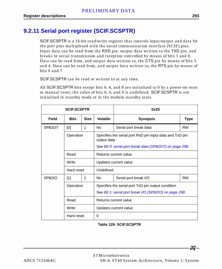
Register descriptions 293PRELIMINARY DATA
9.2.11 Serial port register (SCIF.SCSPTR)
SCIF.SCSPTR is a 16-bit read/write register that controls input/output and data for the port pins multiplexed with the serial communication interface (SCIF) pins. Input data can be read from the RXD pin, output data written to the TXD pin, and breaks in serial transmission and reception controlled by means of bits 1 and 0. Data can be read from, and output data written to, the CTS pin by means of bits 5 and 4. Data can be read from, and output data written to, the RTS pin by means of bits 6 and 7.
SCIF.SCSPTR can be read or written to at any time.
All SCIF.SCSPTR bits except bits 6, 4, and 0 are initialized to 0 by a power-on reset or manual reset; the value of bits 6, 4, and 0 is undefined. SCIF.SCSPTR is not initialized in standby mode or in the module standby state.
SCIF.SCSPTR 0x20
Field Bits Size Volatile Synopsis Type
SPB2DT [0] 1 No Serial port break data RW
Operation Specifies the serial port RxD pin input data and TxD pin output data
See Bit 0: serial port break data (SPB2DT) on page 298.
Read Returns current value
Write Updates current value
Hard reset Undefined
SPB2IO [1] 1 No Serial port break I/O RW
Operation Specifies the serial port TxD pin output condition
See Bit 1: serial port break I/O (SPB2IO) on page 298.
Read Returns current value
Write Updates current value
Hard reset 0
Table 129: SCIF.SCSPTR
STMicroelectronicsADCS 7153464G SH-4, ST40 System Architecture, Volume 1: System
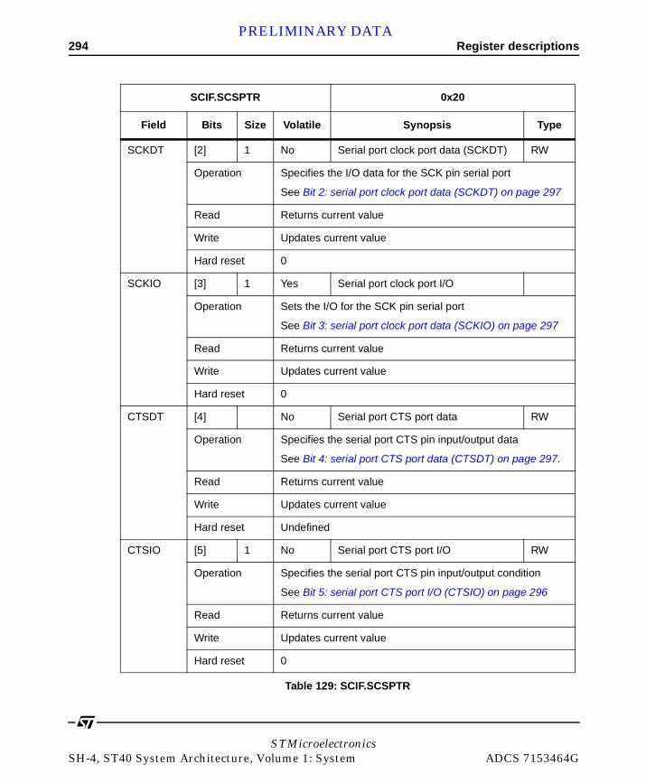
294 Register descriptionsPRELIMINARY DATA
SCKDT [2] 1 No Serial port clock port data (SCKDT) RW
Operation Specifies the I/O data for the SCK pin serial port
See Bit 2: serial port clock port data (SCKDT) on page 297
Read Returns current value
Write Updates current value
Hard reset 0
SCKIO [3] 1 Yes Serial port clock port I/O
Operation Sets the I/O for the SCK pin serial port
See Bit 3: serial port clock port data (SCKIO) on page 297
Read Returns current value
Write Updates current value
Hard reset 0
CTSDT [4] No Serial port CTS port data RW
Operation Specifies the serial port CTS pin input/output data
See Bit 4: serial port CTS port data (CTSDT) on page 297.
Read Returns current value
Write Updates current value
Hard reset Undefined
CTSIO [5] 1 No Serial port CTS port I/O RW
Operation Specifies the serial port CTS pin input/output condition
See Bit 5: serial port CTS port I/O (CTSIO) on page 296
Read Returns current value
Write Updates current value
Hard reset 0
SCIF.SCSPTR 0x20
Field Bits Size Volatile Synopsis Type
Table 129: SCIF.SCSPTR
STMicroelectronicsSH-4, ST40 System Architecture, Volume 1: System ADCS 7153464G

Register descriptions 295PRELIMINARY DATA
Bits 15 to 8: reserved
Bits 15 to 8 are always read as 0, and should only be written with 0.
RTSDT [6] No Serial port RTS port data RW
Operation Specifies the serial port RTS pin input/output data
See Bit 6: serial port RTS port data (RTSDT) on page 296.
Read Returns current value
Write Updates current value
Hard reset Undefined
RTSIO [7] 1 No Serial port RTS port I/O RW
Operation Specifies the serial port RTS pin input/output condition
See Bit 7: serial port RTS port I/O (RTSIO) on page 296.
Read Returns current value
Write Updates current value
Hard reset 0
[8:15] 8 Yes Reserved RO
Operation Reserved
Read 0x00
Write 0 (should only be written with 0)
Hard reset 0
SCIF.SCSPTR 0x20
Field Bits Size Volatile Synopsis Type
Table 129: SCIF.SCSPTR
STMicroelectronicsADCS 7153464G SH-4, ST40 System Architecture, Volume 1: System

296 Register descriptionsPRELIMINARY DATA
Bit 7: serial port RTS port I/O (RTSIO)
Bit 7 specifies the serial port RTS pin input/output condition. When the RTS pin is actually set as a port output pin and outputs the value set by the RTSDT bit, the MCE bit in SCIF.SCFCR should be cleared to 0.
Bit 6: serial port RTS port data (RTSDT)
Bit 6 specifies the serial port RTS pin input/output data. Input or output is specified by the RTSIO bit (see the description of bit 7, RTSIO, for details). In output mode, the RTSDT bit value is output to the RTS pin. The RTS pin value is read from the RTSDT bit regardless of the value of the RTSIO bit. The initial value of this bit after a power-on reset or manual reset is undefined.
Bit 5: serial port CTS port I/O (CTSIO)
Bit 5 specifies the serial port CTS pin input/output condition. When the CTS pin is actually set as a port output pin and outputs the value set by the CTSDT bit, the MCE bit in SCIF.SCFCR should be cleared to 0.
Bit 7: RTSIO Description
0 RTSDT bit value is not output to RTS pin (initial value)
1 RTSDT bit value is output to RTS pin
Bit 6: RTSDT Description
0 Input/output data is low level
1 Input/output data is high level
Bit 5: CTSIO Description
0 CTSDT bit value is not output to CTS pin (initial value)
1 CTSDT bit value is output to CTS pin
STMicroelectronicsSH-4, ST40 System Architecture, Volume 1: System ADCS 7153464G
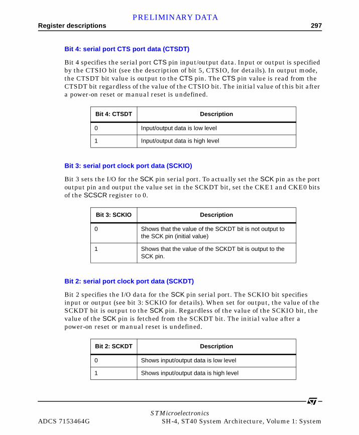
Register descriptions 297PRELIMINARY DATA
Bit 4: serial port CTS port data (CTSDT)
Bit 4 specifies the serial port CTS pin input/output data. Input or output is specified by the CTSIO bit (see the description of bit 5, CTSIO, for details). In output mode, the CTSDT bit value is output to the CTS pin. The CTS pin value is read from the CTSDT bit regardless of the value of the CTSIO bit. The initial value of this bit after a power-on reset or manual reset is undefined.
Bit 3: serial port clock port data (SCKIO)
Bit 3 sets the I/O for the SCK pin serial port. To actually set the SCK pin as the port output pin and output the value set in the SCKDT bit, set the CKE1 and CKE0 bits of the SCSCR register to 0.
Bit 2: serial port clock port data (SCKDT)
Bit 2 specifies the I/O data for the SCK pin serial port. The SCKIO bit specifies input or output (see bit 3: SCKIO for details). When set for output, the value of the SCKDT bit is output to the SCK pin. Regardless of the value of the SCKIO bit, the value of the SCK pin is fetched from the SCKDT bit. The initial value after a power-on reset or manual reset is undefined.
Bit 4: CTSDT Description
0 Input/output data is low level
1 Input/output data is high level
Bit 3: SCKIO Description
0 Shows that the value of the SCKDT bit is not output to the SCK pin (initial value)
1 Shows that the value of the SCKDT bit is output to the SCK pin.
Bit 2: SCKDT Description
0 Shows input/output data is low level
1 Shows input/output data is high level
STMicroelectronicsADCS 7153464G SH-4, ST40 System Architecture, Volume 1: System

298 Register descriptionsPRELIMINARY DATA
Bit 1: serial port break I/O (SPB2IO)
Bit 1 specifies the serial port TXD pin output condition. When the TXD pin is actually set as a port output pin and outputs the value set by the SPB2DT bit, the TE bit in SCIF.SCSCR should be cleared to 0.
Bit 0: serial port break data (SPB2DT)
Bit 0 specifies the serial port RXD pin input data and TXD pin output data. The TXD pin output condition is specified by the SPB2IO bit (see the description of bit 1, SPB2IO, for details). When the TXD pin is designated as an output, the value of the SPB2DT bit is output to the TXD pin. The RXD pin value is read from the SPB2DT bit regardless of the value of the SPB2IO bit. The initial value of this bit after a power-on reset or manual reset is undefined.
Bit 1: SPB2IO Description
0 SPB2DT bit value is not output to the TxD pin (initial value)
1 SPB2DT bit value is output to the TxD pin
Bit 0: SPB2DT
Description
0 Input/output data is low level
1 Input/output data is high level
STMicroelectronicsSH-4, ST40 System Architecture, Volume 1: System ADCS 7153464G

Register descriptions 299PRELIMINARY DATA
SCIF I/O port block diagrams are shown in Figure 34 to Figure 37.
Figure 34: MD8/RTS pin
Reset
Internal data bus
SPTRW
D7
D6
SCIF
RQ DRTSIO
C
Reset
Mode setting register
SPTRR
SPTRW
RQ DRTSDT
C
MD8/RTS2
SPTRW: Write to SPTRSPTRR: Read SPTR
Note: * The RTS2 pin function is designated as modem control by the MCE bit in SCFCR2.
Modem control enable signal*
RTS2 signal
STMicroelectronicsADCS 7153464G SH-4, ST40 System Architecture, Volume 1: System
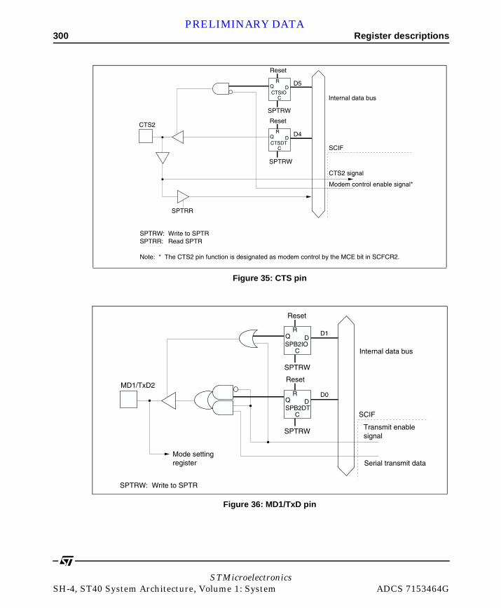
300 Register descriptionsPRELIMINARY DATA
Figure 35: CTS pin
Figure 36: MD1/TxD pin
Reset
Internal data bus
SPTRW
D5
D4
SCIF
RQ DCTSIO
C
Reset
SPTRR
SPTRW
RQ DCTSDT
C
CTS2
SPTRW: Write to SPTRSPTRR: Read SPTR
Note: * The CTS2 pin function is designated as modem control by the MCE bit in SCFCR2.
Modem control enable signal*
CTS2 signal
Reset
Internal data bus
SPTRW
Mode setting register
SCIF
RQ D
D1
D0
SPB2IOC
Reset
SPTRW
RQ DSPB2DT
C
MD1/TxD2
SPTRW: Write to SPTR
Transmit enable signal
Serial transmit data
STMicroelectronicsSH-4, ST40 System Architecture, Volume 1: System ADCS 7153464G
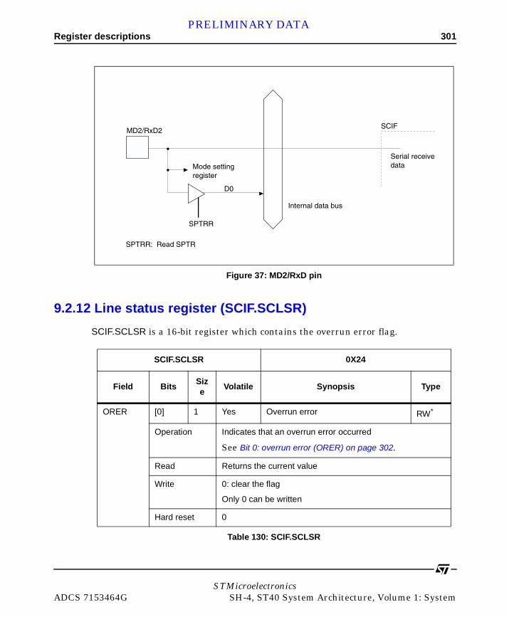
Register descriptions 301PRELIMINARY DATA
9.2.12 Line status register (SCIF.SCLSR)
SCIF.SCLSR is a 16-bit register which contains the overrun error flag.
Figure 37: MD2/RxD pin
Internal data bus
Mode setting register
SCIFMD2/RxD2
SPTRR
D0
Serial receive data
SPTRR: Read SPTR
SCIF.SCLSR 0X24
Field BitsSize
Volatile Synopsis Type
ORER [0] 1 Yes Overrun error RW*
Operation Indicates that an overrun error occurred
See Bit 0: overrun error (ORER) on page 302.
Read Returns the current value
Write 0: clear the flag
Only 0 can be written
Hard reset 0
Table 130: SCIF.SCLSR
STMicroelectronicsADCS 7153464G SH-4, ST40 System Architecture, Volume 1: System
302 Register descriptionsPRELIMINARY DATA
Bits 15 to 1: reserved
Bits 15 to 1 are always read as 0, and should only be written with 0.
Bit 0: overrun error (ORER)
Bit 0 indicates that an overrun error occurred during reception, causing abnormal termination.
[1:15] 15 Yes Reserved RO
Operation Reserved
Read 0
Write 0
Hard reset 0
SCIF.SCLSR 0X24
Field BitsSize
Volatile Synopsis Type
Table 130: SCIF.SCLSR
Bit 0: ORER Description
0 Reception in progress, or reception has ended
normallyA*1 (initial value)
Clearing conditions are:
Power-on reset or manual reset
When 0 is written to ORER after reading ORER = 1
A. The ORER flag is not affected and retains its previous state when the RE bit in SCIF.SCSCR is cleared to 0.
1 An overrun error occurred during receptionB*2
Setting condition is:
When the next serial reception is completed while the receive FIFO is full
STMicroelectronicsSH-4, ST40 System Architecture, Volume 1: System ADCS 7153464G
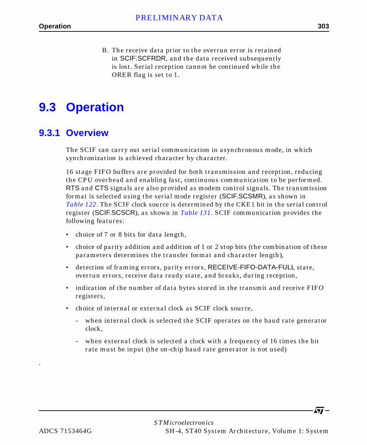
Operation 303PRELIMINARY DATA
9.3 Operation
9.3.1 Overview
The SCIF can carry out serial communication in asynchronous mode, in which synchronization is achieved character by character.
16 stage FIFO buffers are provided for both transmission and reception, reducing the CPU overhead and enabling fast, continuous communication to be performed. RTS and CTS signals are also provided as modem control signals. The transmission format is selected using the serial mode register (SCIF.SCSMR), as shown in Table 122. The SCIF clock source is determined by the CKE1 bit in the serial control register (SCIF.SCSCR), as shown in Table 131. SCIF communication provides the following features:
• choice of 7 or 8 bits for data length,
• choice of parity addition and addition of 1 or 2 stop bits (the combination of these parameters determines the transfer format and character length),
• detection of framing errors, parity errors, RECEIVE-FIFO-DATA-FULL state, overrun errors, receive data ready state, and breaks, during reception,
• indication of the number of data bytes stored in the transmit and receive FIFO registers,
• choice of internal or external clock as SCIF clock source,
- when internal clock is selected the SCIF operates on the baud rate generator clock,
- when external clock is selected a clock with a frequency of 16 times the bit rate must be input (the on-chip baud rate generator is not used)
.
B. The receive data prior to the overrun error is retained in SCIF.SCFRDR, and the data received subsequently is lost. Serial reception cannot be continued while the ORER flag is set to 1.
STMicroelectronicsADCS 7153464G SH-4, ST40 System Architecture, Volume 1: System

304 OperationPRELIMINARY DATA
SCIF.SCSMR settings SCIF transfer format
Bit 6:
CHR
Bit 5: PE
Bit 3: STO
PMode
Data length
Multiprocessor bit
Parity bit
Stop bit
length
0 0 0 Asynchronous mode
8-bit data
No No 1 bit
- - 1 - - - - 2 bits
- 1 0 - - - Yes 1 bit
- - 1 - - - - 2 bits
1 0 0 - 7-bit data
- No 1 bit
- - 1 - - - - 2 bits
- 1 0 - - - Yes 1 bit
- - 1 - - - - 2 bits
SCIF.SCSCR setting SCIF transmit/receive clock
Bit 1: CKE1
Bit 0: CKE0
ModeClock source
SCK pin function
0 0 Asynchronous mode
Internal SCIF does not use SCK pin
0 1 Asynchronous mode
Internal Output clock with frequency of 16 times the bit rate.
1 0 Asynchronous mode
External Inputs clock with frequency of 16 times the bit rate
1 1 Asynchronous mode
External Inputs clock with frequency of 16 times the bit rate
Table 131: SCIF.SCSCR settings for SCIF clock source selection
STMicroelectronicsSH-4, ST40 System Architecture, Volume 1: System ADCS 7153464G

Operation 305PRELIMINARY DATA
9.3.2 Serial operation
Data transfer format
Table 132 shows the data transfer formats that can be used. Any of the 8 transfer formats can be selected according to the SCIF.SCSMR settings. In Table 132 S = start bit, STOP = stop bit and P = parity bit.
SCIF.SCSMR settings Serial transfer format and frame length
CHR PE STOP 1 2 3 4 5 6 7 8 9 10 11 12
0 0 0 S 8-bit data STOP
0 0 1 S 8-bit data STOP STOP
0 1 0 S 8-bit data P STOP
0 1 1 S 8-bit data P STOP STOP
1 0 0 S 7-bit data STOP
1 0 1 S 7-bit data STOP STOP
1 1 0 S 7-bit data P STOP
1 1 1 S 7-bit data P STOP STOP
Table 132: Serial transfer formats
STMicroelectronicsADCS 7153464G SH-4, ST40 System Architecture, Volume 1: System

306 OperationPRELIMINARY DATA
Clock
Either an internal clock generated by the on-chip baud rate generator or an external clock input at the SCK pin can be selected as the SCIF’s serial clock, according to the setting of the CKE1 bit in SCIF.SCSCR. For details of SCIF clock source selection, see Table 131.
When an external clock is input at the SCK pin, the clock frequency should be 16 times the bit rate used.
Data transfer operations
SCIF initialization
Before transmitting and receiving data, it is necessary to clear the TE and RE bits in SCIF.SCSCR to 0, then initialize the SCIF as described below.
When the transfer format is changed, the TE and RE bits must be cleared to 0 before making the change using the following procedure. When the TE bit is cleared to 0, SCIF.SCTSR is initialized.
Note: clearing the TE and RE bits to 0 does not change the contents of SCIF.SCFSR, SCIF.SCFTDR, or SCIF.SCFRDR.
The TE bit should be cleared to 0 after all transmit data has been sent and the TEND flag in SCIF.SCFSR has been set. TEND can also be cleared to 0 during transmission, but the data being transmitted will go to the mark state after the clearance. Before setting TE again to start transmission, the TFRST bit in SCIF.SCFCR should first be set to 1 to reset SCIF.SCFTDR.
When an external clock is used the clock should not be stopped during operation, including initialization, since operation will be unreliable in this case.
Figure 38 shows a sample SCIF initialization flowchart.
STMicroelectronicsSH-4, ST40 System Architecture, Volume 1: System ADCS 7153464G

Operation 307PRELIMINARY DATA
Figure 38: Sample SCIF initialization flowchart
Initialization
Clear TE and RE bitsin SCSCR2 to 0
Set TFRST and RFRST bitsin SCFCR2 to 1
Set CKE1 bit in SCSCR2 (leaving TE and RE bits
cleared to 0)
Set data transfer formatin SCSMR2
Set value in SCBRR2
1-bit interval elapsed?
Set RTRG1–0, TTRG1–0,and MCE bits in SCFCR2
Clear TFRST and RFRST bits to 0
Set TE and RE bitsin SCSCR2 to 1,
and set RIE, TIE, and REIE bits
End
Wait
No
Yes
1. Set the clock selection in SCSCR2.
Be sure to clear bits RIE and TIE, and bits TE and RE, to 0.
2. Set the data transfer format in SCSMR2.
3. Write a value corresponding to the bit rate into SCBRR2. (Not necessary if an external clock is used.)
4. Wait at least one bit interval, then set the TE bit or RE bit in SCSCR2 to 1. Also set the RIE, REIE, and TIE bits.
Setting the TE and RE bits enables the TxD2 and RxD2 pins to be used. When transmitting, the SCIF will go to the mark state; when receiving, it will go to the idle state, waiting for a start bit.
STMicroelectronicsADCS 7153464G SH-4, ST40 System Architecture, Volume 1: System

308 OperationPRELIMINARY DATA
Serial data transmission
Figure 39 shows a sample flowchart for serial transmission.
Use the following procedure for serial data transmission after enabling the SCIF for transmission.
Figure 39: Sample serial transmission flowchart
Start of transmission
Read TDFE flag in SCFSR2
TDFE = 1?
Write transmit data (16 - transmittrigger set number) to SCFTDR2,read 1 from TDFE flag and TENDflag in SCFSR2, then clear to 0
All data transmitted?
Read TEND flag in SCFSR2
TEND = 1?
Break output?
Clear SPB2DT to 0 andset SPB2IO to 1
Clear TE bit in SCSCR2 to 0
End of transmission
No
Yes
No
Yes
No
Yes
No
Yes
1. SCIF status check and transmit data write:
Read SCFSR2 and check that the TDFE flag is set to 1, then write transmit data to SCFTDR2, read 1 from the TDFE and TEND flags, then clear these flags to 0.
The number of transmit data bytes that can be written is 16 - (transmit trigger set number).
2. Serial transmission continuation procedure:
To continue serial transmission, read 1 from the TDFE flag to confirm that writing is possible, then write data to SCFTDR2, and then clear the TDFE flag to 0.
3. Break output at the end of serial transmission:
To output a break in serial transmission, clear the SPB2DT bit to 0 and set the SPB2IO bit to 1 in SCSPTR2, then clear the TE bit in SCSCR2 to 0.
In steps 1 and 2, it is possible to ascertain the number of data bytes that can be written from the number of transmit data bytes in SCFTDR2 indicated by the upper 8 bits of SCFDR2.
STMicroelectronicsSH-4, ST40 System Architecture, Volume 1: System ADCS 7153464G

Operation 309PRELIMINARY DATA
In serial transmission, the SCIF operates as described below.
1 When data is written into SCIF.SCFTDR, the SCIF transfers the data from SCIF.SCFTDR to SCIF.SCTSR and starts transmitting. Confirm that the TDFE flag in the serial status register (SCIF.SCFSR) is set to 1 before writing transmit data to SCIF.SCFTDR. The number of data bytes that can be written is at least 16 (transmit trigger setting).
2 When data is transferred from SCIF.SCFTDR to SCIF.SCTSR and transmission is started, consecutive transmit operations are performed until there is no transmit data left in SCIF.SCFTDR. When the number of transmit data bytes in SCIF.SCFTDR falls to or below the transmit trigger number set in the FIFO control register (SCIF.SCFCR), the TDFE flag is set. If the TIE bit in SCIF.SCSCR is set to 1 at this time, a TRANSMIT-FIFO-DATA-EMPTY interrupt (TXI) request is generated. The serial transmit data is sent from the TXD pin in the following order:
2.1 start bit: one 0-bit is output,
2.2 transmit data: 8-bit or 7-bit data is output in LSB first order,
2.3 parity bit: 1 parity bit (even or odd parity) is output (a format in which a parity bit is not output can also be selected),
2.4 stop bit(s): 1 or two 1-bits (stop bits) are output,
2.5 mark state: 1 is output continuously until the start bit that starts the next transmission is sent.
3 The SCIF checks the SCIF.SCFTDR transmit data at the timing for sending the stop bit. If data is present, the data is transferred from SCIF.SCFTDR to SCIF.SCTSR, the stop bit is sent, and then serial transmission of the next frame is started. If there is no transmit data, the TEND flag in SCIF.SCFSR is set to 1, the stop bit is sent, and then the line goes to the mark state in which 1 is output.
Figure 40 shows an example of the operation for transmission in asynchronous mode.
STMicroelectronicsADCS 7153464G SH-4, ST40 System Architecture, Volume 1: System
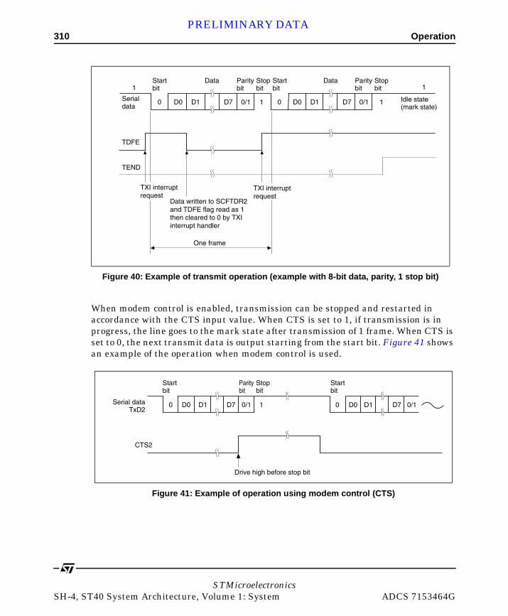
310 OperationPRELIMINARY DATA
When modem control is enabled, transmission can be stopped and restarted in accordance with the CTS input value. When CTS is set to 1, if transmission is in progress, the line goes to the mark state after transmission of 1 frame. When CTS is set to 0, the next transmit data is output starting from the start bit. Figure 41 shows an example of the operation when modem control is used.
Figure 40: Example of transmit operation (example with 8-bit data, parity, 1 stop bit)
1
0 D0 D1 D7 0/1 1 0 D0 D1 D7 0/1 1
1
TDFE
TEND
Serial data
Start bit
Data Parity bit
Stop bit
Start bit
Idle state (mark state)
Data Parity bit
Stop bit
TXI interrupt request
Data written to SCFTDR2 and TDFE flag read as 1 then cleared to 0 by TXI interrupt handler
One frame
TXI interrupt request
Figure 41: Example of operation using modem control (CTS)
Serial dataTxD2
0 D0 D1 D7 0/1 01 D0 D1 D7 0/1
CTS2
Drive high before stop bit
Startbit
Paritybit
Stopbit
Startbit
STMicroelectronicsSH-4, ST40 System Architecture, Volume 1: System ADCS 7153464G
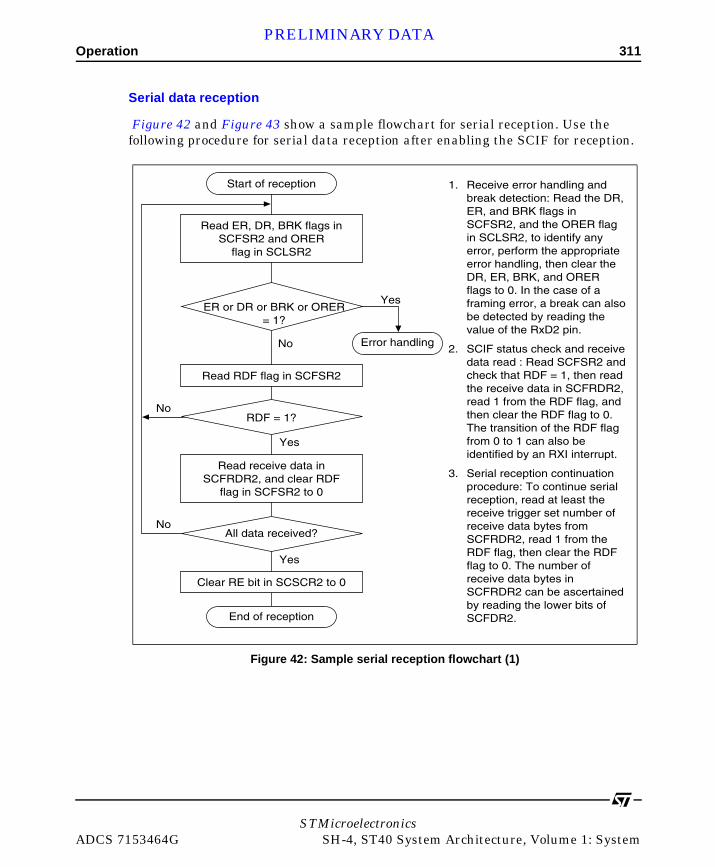
Operation 311PRELIMINARY DATA
Serial data reception
Figure 42 and Figure 43 show a sample flowchart for serial reception. Use the following procedure for serial data reception after enabling the SCIF for reception.
Figure 42: Sample serial reception flowchart (1)
Start of reception
Read ER, DR, BRK flags inSCFSR2 and ORER
flag in SCLSR2
ER or DR or BRK or ORER= 1?
Read RDF flag in SCFSR2
RDF = 1?
Read receive data inSCFRDR2, and clear RDF
flag in SCFSR2 to 0
All data received?
Clear RE bit in SCSCR2 to 0
End of reception
Yes
No
Yes
Yes
No
No
Error handling
1. Receive error handling and break detection: Read the DR, ER, and BRK flags in SCFSR2, and the ORER flag in SCLSR2, to identify any error, perform the appropriate error handling, then clear the DR, ER, BRK, and ORER flags to 0. In the case of a framing error, a break can also be detected by reading the value of the RxD2 pin.
2. SCIF status check and receive data read : Read SCFSR2 and check that RDF = 1, then read the receive data in SCFRDR2, read 1 from the RDF flag, and then clear the RDF flag to 0. The transition of the RDF flag from 0 to 1 can also be identified by an RXI interrupt.
3. Serial reception continuation procedure: To continue serial reception, read at least the receive trigger set number of receive data bytes from SCFRDR2, read 1 from the RDF flag, then clear the RDF flag to 0. The number of receive data bytes in SCFRDR2 can be ascertained by reading the lower bits of SCFDR2.
STMicroelectronicsADCS 7153464G SH-4, ST40 System Architecture, Volume 1: System

312 OperationPRELIMINARY DATA
In serial reception, the SCIF operates as described below.
Figure 43: Sample serial reception flowchart (2)
Error handling
Receive error handling
ER = 1?
BRK = 1?
Break handling
DR = 1?
Read receive data in SCFRDR2
Clear DR, ER, BRK flags in SCFSR2,
and ORER flag in SCLSR2, to 0
End
Yes
Yes
Yes
No
Overrun error handling
ORER = 1?
Yes
No
No
No
1. Whether a framing error or parity error has occurred in the receive data read from SCFRDR2 can be ascertained from the FER and PER bits in SCFSR2.
2. When a break signal is received, receive data is not transferred to SCFRDR2 while the BRK flag is set. However, note that the last data in SCFRDR2 is H'00 (the break data in which a framing error occurred is stored).
STMicroelectronicsSH-4, ST40 System Architecture, Volume 1: System ADCS 7153464G
Operation 313PRELIMINARY DATA
1 The SCIF monitors the transmission line, and if a 0 start bit is detected, performs internal synchronization and starts reception.
2 The received data is stored in SCIF.SCRSR in LSB to MSB order.
3 The parity bit and stop bit are received. After receiving these bits, the SCIF carries out the following checks:
3.1 stop bit check: the SCIF checks whether the stop bit is 1 (if there are 2 stop bits, only the first is checked),
3.2 the SCIF checks whether receive data can be transferred from the receive shift register (SCIF.SCRSR) to SCIF.SCFRDR,
3.3 overrun error check: the SCIF checks that the ORER flag is 0, indicating that no overrun error has occurred,
3.4 break check: the SCIF checks that the BRK flag is 0, indicating that the break state is not set. If all the above checks are passed, the receive data is stored in SCIF.SCFRDR.
Note: Reception continues when a receive error occurs.
4 If the RIE bit in SCIF.SCSCR is set to 1 when the RDF or DR flag changes to 1, a RECEIVE-FIFO-DATA-FULL interrupt (RXI) request is generated. If the RIE bit or REIE bit in SCIF.SCSCR is set to 1 when the ER flag changes to 1, a receive error interrupt (ERI) request is generated. If the RIE bit or REIE bit in SCIF.SCSCR is set to 1 when the BRK or ORER flag changes to 1, a break reception interrupt (BRI) request is generated.
Figure 44 shows an example of the operation for reception.
STMicroelectronicsADCS 7153464G SH-4, ST40 System Architecture, Volume 1: System
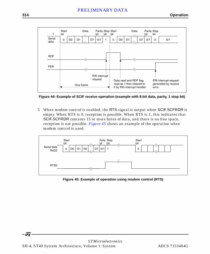
314 OperationPRELIMINARY DATA
5 When modem control is enabled, the RTS signal is output when SCIF.SCFRDR is empty. When RTS is 0, reception is possible. When RTS is 1, this indicates that SCIF.SCFRDR contains 15 or more bytes of data, and there is no free space, reception is not possible. Figure 45 shows an example of the operation when modem control is used.
Figure 44: Example of SCIF receive operation (example with 8-bit data, parity, 1 stop bit)
1
0 D0 D1 D7 0/1 1 0 D0 D1 D7 0/1 0/10
RDF
FER
Serial data
Start bit
Data Parity bit
Stop bit
Start bit
Data Parity bit
Stop bit
RXI interrupt request
One frame
Data read and RDF flag read as 1 then cleared to 0 by RXI interrupt handler
ERI interrupt request generated by receive error
Figure 45: Example of operation using modem control (RTS)
D0 D1 D2 D7 0/1 1 00
RTS2
Serial dataRxD2
Start bit
Parity bit
Stopbit
Start bit
STMicroelectronicsSH-4, ST40 System Architecture, Volume 1: System ADCS 7153464G
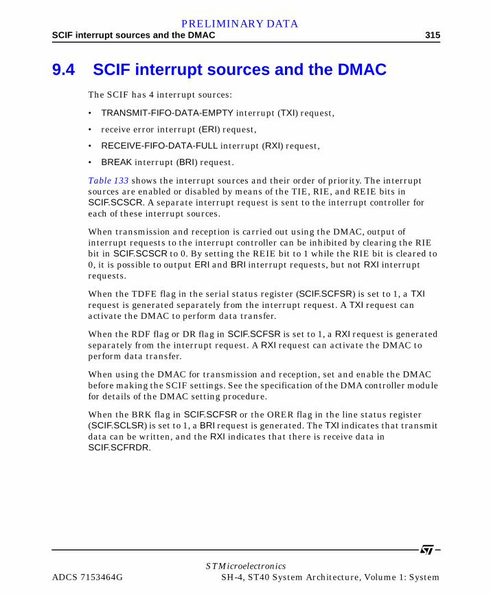
SCIF interrupt sources and the DMAC 315PRELIMINARY DATA
9.4 SCIF interrupt sources and the DMACThe SCIF has 4 interrupt sources:
• TRANSMIT-FIFO-DATA-EMPTY interrupt (TXI) request,
• receive error interrupt (ERI) request,
• RECEIVE-FIFO-DATA-FULL interrupt (RXI) request,
• BREAK interrupt (BRI) request.
Table 133 shows the interrupt sources and their order of priority. The interrupt sources are enabled or disabled by means of the TIE, RIE, and REIE bits in SCIF.SCSCR. A separate interrupt request is sent to the interrupt controller for each of these interrupt sources.
When transmission and reception is carried out using the DMAC, output of interrupt requests to the interrupt controller can be inhibited by clearing the RIE bit in SCIF.SCSCR to 0. By setting the REIE bit to 1 while the RIE bit is cleared to 0, it is possible to output ERI and BRI interrupt requests, but not RXI interrupt requests.
When the TDFE flag in the serial status register (SCIF.SCFSR) is set to 1, a TXI request is generated separately from the interrupt request. A TXI request can activate the DMAC to perform data transfer.
When the RDF flag or DR flag in SCIF.SCFSR is set to 1, a RXI request is generated separately from the interrupt request. A RXI request can activate the DMAC to perform data transfer.
When using the DMAC for transmission and reception, set and enable the DMAC before making the SCIF settings. See the specification of the DMA controller module for details of the DMAC setting procedure.
When the BRK flag in SCIF.SCFSR or the ORER flag in the line status register (SCIF.SCLSR) is set to 1, a BRI request is generated. The TXI indicates that transmit data can be written, and the RXI indicates that there is receive data in SCIF.SCFRDR.
STMicroelectronicsADCS 7153464G SH-4, ST40 System Architecture, Volume 1: System

316 Usage notesPRELIMINARY DATA
See the Exceptions chapter of the CPU Architecture manual, for priorities and the relationship with non-SCIF interrupts.
9.5 Usage notesNote the following when using the SCIF.
9.5.1 SCIF.SCFTDR writing and the TDFE flag
The TDFE flag in the serial status register (SCIF.SCFSR) is set when the number of transmit data bytes written in the transmit FIFO data register (SCIF.SCFTDR) has fallen to or below the transmit trigger number set by bits TTRG1 and TTRG0 in the FIFO control register (SCIF.SCFCR). After TDFE is set, transmit data up to the number of empty bytes in SCIF.SCFTDR can be written, allowing efficient continuous transmission.
However, if the number of data bytes written in SCIF.SCFTDR is equal to or less than the transmit trigger number, the TDFE flag will be set to 1 again after being read as 1 and cleared to 0. TDFE clearing should therefore be carried out when SCIF.SCFTDR contains more than the transmit trigger number of transmit data bytes.
The number of transmit data bytes in SCIF.SCFTDR can be found from the upper 8 bits of the FIFO data count register (SCIF.SCFDR).
Interrupt source
DescriptionDMAC
activation
Priority on reset
release
ERI Interrupt initiated by receive-error flag (ER) Not possible High
Low
RXI Interrupt initiated by receive-FIFO-data-full flag (RDF) or receive data ready flag (DR)
Possible
BRI Interrupt initiated by break flag (BRK) or overrun error flag (ORER)
Not possible
TXI Interrupt initiated by TRANSMIT-FIFO-DATA-EMPTY flag (TDFE)
Possible
Table 133: SCIF interrupt sources
STMicroelectronicsSH-4, ST40 System Architecture, Volume 1: System ADCS 7153464G

Usage notes 317PRELIMINARY DATA
9.5.2 SCIF.SCFRDR reading and the RDF flag
The RDF flag in the serial status register (SCIF.SCFSR) is set when the number of receive data bytes in the receive FIFO data register (SCIF.SCFRDR) has become equal to or greater than the receive trigger number set by bits RTRG1 and RTRG0 in the FIFO control register (SCIF.SCFCR). After RDF is set, receive data equivalent to the trigger number can be read from SCIF.SCFRDR, allowing efficient continuous reception.
However, if the number of data bytes in SCIF.SCFRDR is equal to or greater than the trigger number, the RDF flag will be set to 1 again if it is cleared to 0. RDF should therefore be cleared to 0 after being read as 1 after all the receive data has been read.
The number of receive data bytes in SCIF.SCFRDR can be found from the lower 8 bits of the FIFO data count register (SCIF.SCFDR).
9.5.3 Break detection and processing
BREAK signals can be detected by reading the RXD pin directly when a framing error (FER) is detected. In the BREAK state the input from the RXD pin consists of all 0s, so the FER flag is set and the parity error flag (PER) may also be set. Although the SCIF stops transferring receive data to SCIF.SCFRDR after receiving a BREAK, the receive operation continues.
9.5.4 Sending a break signal
The input/output condition and level of the TXD pin are determined by bits SPB2IO and SPB2DT in the serial port register (SCIF.SCSPTR). This feature can be used to send a BREAK signal.
After the serial transmitter is initialized, the TXD pin function is not selected and the value of the SPB2DT bit substitutes for the mark state until the TE bit is set to 1 (that is transmission is enabled). The SPB2IO and SPB2DT bits should therefore be set to 1 (designating output and high level) beforehand.
To send a BREAK signal during serial transmission, clear the SPB2DT bit to 0 (designating low level), then clear the TE bit to 0 (halting transmission). When the TE bit is cleared to 0, the transmitter is initialized, regardless of its current state, and 0 is output from the TXD pin.
STMicroelectronicsADCS 7153464G SH-4, ST40 System Architecture, Volume 1: System
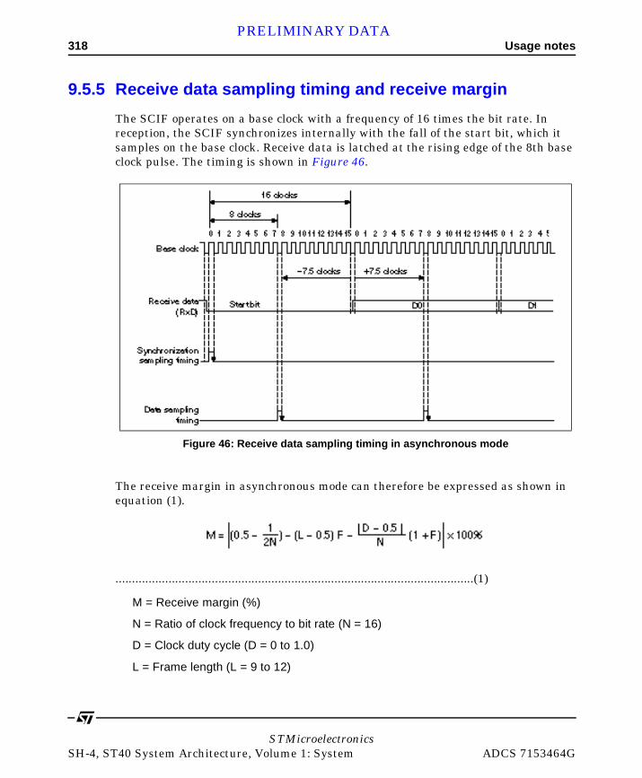
318 Usage notesPRELIMINARY DATA
9.5.5 Receive data sampling timing and receive margin
The SCIF operates on a base clock with a frequency of 16 times the bit rate. In reception, the SCIF synchronizes internally with the fall of the start bit, which it samples on the base clock. Receive data is latched at the rising edge of the 8th base clock pulse. The timing is shown in Figure 46.
The receive margin in asynchronous mode can therefore be expressed as shown in equation (1).
............................................................................................................(1)
M = Receive margin (%)
N = Ratio of clock frequency to bit rate (N = 16)
D = Clock duty cycle (D = 0 to 1.0)
L = Frame length (L = 9 to 12)
Figure 46: Receive data sampling timing in asynchronous mode
STMicroelectronicsSH-4, ST40 System Architecture, Volume 1: System ADCS 7153464G

Usage notes 319PRELIMINARY DATA
F = Absolute deviation of clock frequency
From equation (1), if F = 0 and D = 0.5, the receive margin is 46.875%, as given by equation (2).
When D = 0.5 and F = 0:
M = (0.5 – 1 / (2 × 16) ) × 100% = 46.875% ....................................................(2)
This is a theoretical value. A reasonable margin to allow in system designs is 20% to 30%.
9.5.6 SCK/MRESET
As the manual reset pin is multiplexed with the SCK pin, a manual reset must not be executed while the SCIF is operating in external clock mode.
9.5.7 When using the DMAC
When using the DMAC for transmission and reception, inhibit output of RXI and TXI requests to the interrupt controller. If interrupt request output is enabled, interrupt requests to the interrupt controller will be cleared by the DMAC without regard to the interrupt handler.
9.5.8 Serial ports
Note: when the SCIF pin value is read using a serial port, the value read will be the value 2 peripheral clock cycles earlier.
STMicroelectronicsADCS 7153464G SH-4, ST40 System Architecture, Volume 1: System

320 Usage notesPRELIMINARY DATA
STMicroelectronicsSH-4, ST40 System Architecture, Volume 1: System ADCS 7153464G

PRELIMINARY DATA
STMicroelectroniADCS 7153464G SH-4, ST40 S
10
User break controller (UBC) 10.1 OverviewThe user break controller (UBC) provides functions that simplify program debugging. When break conditions are set in the UBC, a user break interrupt is generated according to the contents of the bus cycle generated by the CPU. This function makes it easy to design an effective self-monitoring debugger, enabling programs to be debugged with the chip alone, without using an in-circuit emulator.
10.1.1 Features
The UBC has the features described below.
• Two break channels (A and B): user break interrupts can be generated on independent conditions for channels A and B, or on sequential conditions (sequential break setting: channel A then channel B).
• Five break compare conditions:
- address (selection of 32-bit virtual address and ASID for comparison),
- data: channel B only, 32-bit mask capability,
- bus cycle: instruction access or operand access,
- read/write,
- operand size: byte, word, longword, quadword.
csystem Architecture, Volume 1: System
322 OverviewPRELIMINARY DATA
• Address comparison has the following options:
- all bits compared,
- lower 10 bits masked,
- lower 12 bits masked,
- lower 16 bits masked,
- lower 20 bits masked,
- all bits masked.
• ASID comparison has the following options:
- all bits compared,
- all bits masked.
• An instruction access cycle break can be effected before or after the instruction is executed.
STMicroelectronicsSH-4, ST40 System Architecture, Volume 1: System ADCS 7153464G
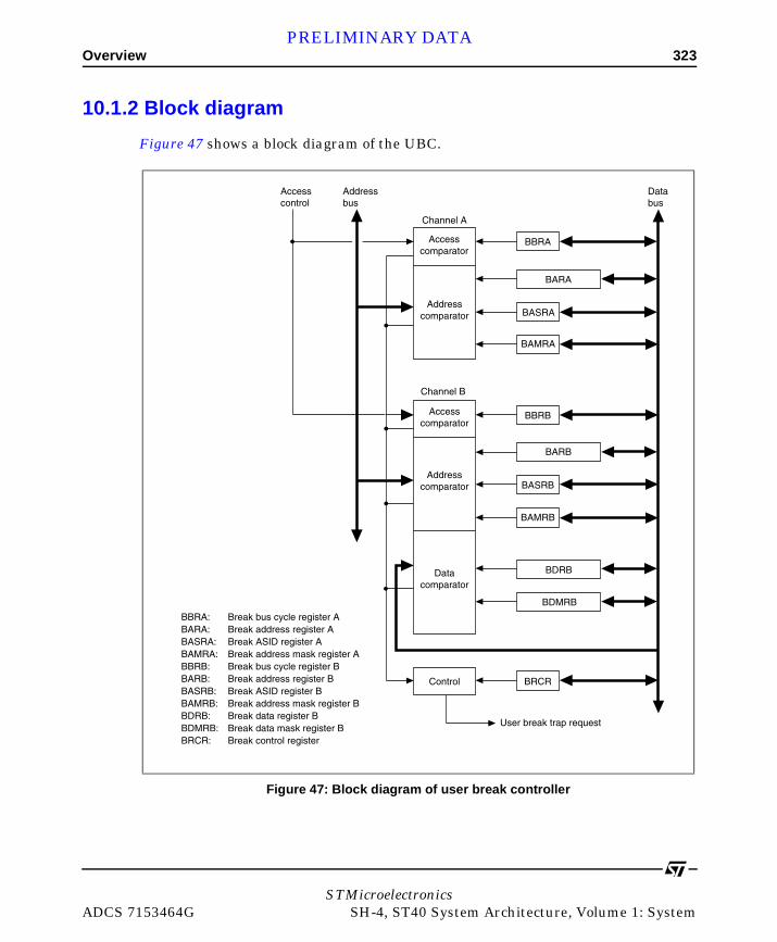
Overview 323PRELIMINARY DATA
10.1.2 Block diagram
Figure 47 shows a block diagram of the UBC.
Figure 47: Block diagram of user break controller
Access control
Addressbus
Databus
Channel A
Accesscomparator
Addresscomparator
Channel B
Accesscomparator
Addresscomparator
Datacomparator
BBRA
BARA
BASRA
BAMRA
BBRB
BARB
BASRB
BAMRB
BDRB
BDMRB
BRCRControl
User break trap request
BBRA: Break bus cycle register ABARA: Break address register ABASRA: Break ASID register ABAMRA: Break address mask register ABBRB: Break bus cycle register BBARB: Break address register BBASRB: Break ASID register BBAMRB: Break address mask register BBDRB: Break data register BBDMRB: Break data mask register BBRCR: Break control register
STMicroelectronicsADCS 7153464G SH-4, ST40 System Architecture, Volume 1: System

324 Register overviewPRELIMINARY DATA
10.2 Register overviewTable 134 shows a summary of the UBC registers.
Register name
Description TypeAddress offset
Access size
Initial value
P4 Area
UBC.BARA Break address register A,see Section 10.3.2: Break address register A (UBC.BARA) on page 328
RW 0xFF200000 0x1F200000 32 Undefined
UBC.BAMRA Break address mask register A,see Section 10.3.4: Break address mask register A (UBC.BAMRA) on page 329
RW 0xFF200004 0x1F200004 8 Undefined
UBC.BBRA Break bus cycle register A,see Section 10.3.5: Break bus cycle register A (UBC.BBRA) on page 331
RW 0xFF200008 0x1F200008 16 0x0000
UBC.BASRA Break ASID register A,see Section 10.3.3: Break ASID register A (UBC.BASRA) on page 329
RW 0xFF000014 0x1F000014 8 Undefined
Table 134: UBC registers
STMicroelectronicsSH-4, ST40 System Architecture, Volume 1: System ADCS 7153464G
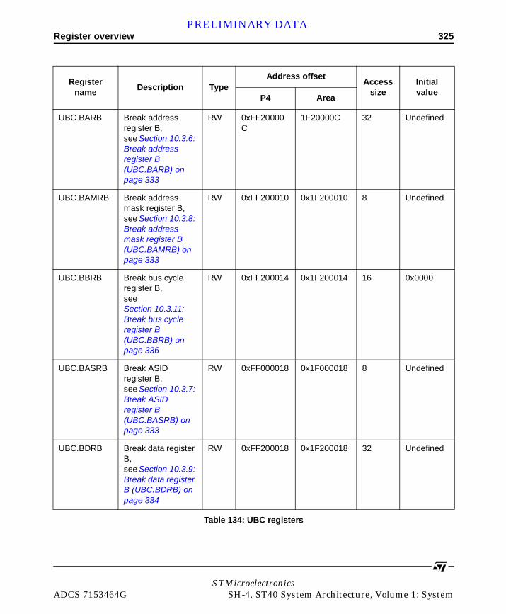
Register overview 325PRELIMINARY DATA
UBC.BARB Break address register B,see Section 10.3.6: Break address register B (UBC.BARB) on page 333
RW 0xFF20000C
1F20000C 32 Undefined
UBC.BAMRB Break address mask register B,see Section 10.3.8: Break address mask register B (UBC.BAMRB) on page 333
RW 0xFF200010 0x1F200010 8 Undefined
UBC.BBRB Break bus cycle register B,see Section 10.3.11: Break bus cycle register B (UBC.BBRB) on page 336
RW 0xFF200014 0x1F200014 16 0x0000
UBC.BASRB Break ASID register B,see Section 10.3.7: Break ASID register B (UBC.BASRB) on page 333
RW 0xFF000018 0x1F000018 8 Undefined
UBC.BDRB Break data register B,see Section 10.3.9: Break data register B (UBC.BDRB) on page 334
RW 0xFF200018 0x1F200018 32 Undefined
Register name
Description TypeAddress offset
Access size
Initial value
P4 Area
Table 134: UBC registers
STMicroelectronicsADCS 7153464G SH-4, ST40 System Architecture, Volume 1: System

326 Register overviewPRELIMINARY DATA
UBC.BDMRB Break data mask register B,see Section 10.3.10: Break data mask register B (UBC.BDMRB) on page 335
RW 0xFF20001C
0x1F20001C 32 Undefined
UBC.BRCR Break control register,see Section 10.3.12: Break control register (UBC.BRCR) on page 337
RW 0xFF200020 0x1F200020 16 0x0000A
A. Some bits are not initialized. See Section 10.3.12: Break control register (UBC.BRCR) on page 337, for details.
Register name
Description TypeAddress offset
Access size
Initial value
P4 Area
Table 134: UBC registers
STMicroelectronicsSH-4, ST40 System Architecture, Volume 1: System ADCS 7153464G

Register descriptions 327PRELIMINARY DATA
10.3 Register descriptions
10.3.1 Access to UBC control registers
The access size must be the same as the control register size. If the sizes are different, a write will not be effected in a UBC register write operation, and a read operation will return an undefined value. UBC control register contents cannot be transferred to a floating-point register using a floating-point memory load instruction.
When a UBC control register is updated, use either of the following methods to make the updated value valid.
• Execute an RTE instruction after the memory store instruction that updated the register. The updated value will be valid from the RTE instruction jump destination onward.
• Execute instructions requiring 5 states for execution after the memory store instruction that updated the register. As the ST40 executes 2 instructions in parallel and a minimum of 0.5 state is required for execution of 1 instruction, 11 instructions must be inserted. The updated value will be valid from the 6th state onward.
STMicroelectronicsADCS 7153464G SH-4, ST40 System Architecture, Volume 1: System

328 Register descriptionsPRELIMINARY DATA
10.3.2 Break address register A (UBC.BARA)
Break address register A (UBC.BARA) is a 32-bit read/write register that specifies the virtual address used in the channel A break conditions. UBC.BARA is not initialized by a power-on reset or manual reset.
Bit 31 30 29 28 27 26 25 24
BAA31 BAA30 BAA29 BAA28BAA2
7BAA26
BAA25
BAA24
Initial value - - - - - - - -
Type RW RW RW RW RW RW RW RW
Bit 23 22 21 20 19 18 17 16
BAA23 BAA22 BAA21 BAA20BAA1
9BAA18
BAA17
BAA16
Initial value - - - - - - - -
Type RW RW RW RW RW RW RW RW
Bit 15 14 13 12 11 10 9 8
BAA15 BAA14 BAA13 BAA12 BAA11 BAA10 BAA9 BAA8
Initial value - - - - - - - -
Type RW RW RW RW RW RW RW RW
Bit 7 6 5 4 3 2 1 0
BAA7 BAA6 BAA5 BAA4 BAA3 BAA2 BAA1 BAA0
Initial value - - - - - - - -
Type RW RW RW RW RW RW RW RW
STMicroelectronicsSH-4, ST40 System Architecture, Volume 1: System ADCS 7153464G
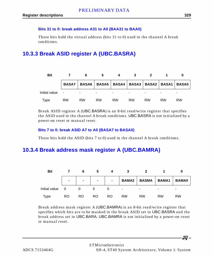
Register descriptions 329PRELIMINARY DATA
Bits 31 to 0: break address A31 to A0 (BAA31 to BAA0)
These bits hold the virtual address (bits 31 to 0) used in the channel A break conditions.
10.3.3 Break ASID register A (UBC.BASRA)
Break ASID register A (UBC.BASRA) is an 8-bit read/write register that specifies the ASID used in the channel A break conditions. UBC.BASRA is not initialized by a power-on reset or manual reset.
Bits 7 to 0: break ASID A7 to A0 (BASA7 to BASA0)
These bits hold the ASID (bits 7 to 0) used in the channel A break conditions.
10.3.4 Break address mask register A (UBC.BAMRA)
Break address mask register A (UBC.BAMRA) is an 8-bit read/write register that specifies which bits are to be masked in the break ASID set in UBC.BASRA and the break address set in UBC.BARA. UBC.BAMRA is not initialized by a power-on reset or manual reset.
Bit 7 6 5 4 3 2 1 0
BASA7 BASA6 BASA5 BASA4 BASA3 BASA2 BASA1 BASA0
Initial value - - - - - - - -
Type RW RW RW RW RW RW RW RW
Bit 7 6 5 4 3 2 1 0
- - - - BAMA2 BASMA BAMA1 BAMA0
Initial value 0 0 0 0 - - - -
Type RO RO RO RO RW RW RW RW
STMicroelectronicsADCS 7153464G SH-4, ST40 System Architecture, Volume 1: System
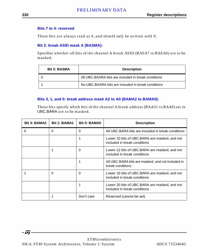
330 Register descriptionsPRELIMINARY DATA
Bits 7 to 4: reserved
These bits are always read as 0, and should only be written with 0.
Bit 2: break ASID mask A (BASMA):
Specifies whether all bits of the channel A break ASID (BASA7 to BASA0) are to be masked.
Bits 3, 1, and 0: break address mask A2 to A0 (BAMA2 to BAMA0):
These bits specify which bits of the channel A break address (BAA31 to BAA0) set in UBC.BARA are to be masked.
Bit 2: BASMA Description
0 All UBC.BASRA bits are included in break conditions
1 No UBC.BASRA bits are included in break conditions
Bit 3: BAMA2 Bit 1: BAMA1 Bit 0: BAMA0 Description
0 0 0 All UBC.BARA bits are included in break conditions
1 Lower 10 bits of UBC.BARA are masked, and not included in break conditions
1 0 Lower 12 bits of UBC.BARA are masked, and not included in break conditions
1 All UBC.BARA bits are masked, and not included in break conditions
1 0 0 Lower 16 bits of UBC.BARA are masked, and not included in break conditions
1 Lower 20 bits of UBC.BARA are masked, and not included in break conditions
1 Don’t care Reserved (cannot be set)
STMicroelectronicsSH-4, ST40 System Architecture, Volume 1: System ADCS 7153464G

Register descriptions 331PRELIMINARY DATA
10.3.5 Break bus cycle register A (UBC.BBRA)
Break bus cycle register A (UBC.BBRA) is a 16-bit read/write register that sets 3 conditions:
• instruction access/operand access,
• read/write,
• operand size
from among the channel A break conditions.
UBC.BBRA is initialized to 0x0000 by a power-on reset or manual reset. It retains its value in standby mode.
Bits 15 to 7: reserved
These bits are always read as 0, and should only be written with 0.
Bit 15 14 13 12 11 10 9 8
- - - - - - - -
Initial value
0 0 0 0 0 0 0 0
Type RO RO RO RO RO RO RO RO
Bit 7 6 5 4 3 2 1 0
- SZA2 IDA1 IDA0 RWA1 RWA0 SZA1 SZA0
Initial value
0 0 0 0 0 0 0 0
Type RO RW RW RW RW RW RW RW
STMicroelectronicsADCS 7153464G SH-4, ST40 System Architecture, Volume 1: System
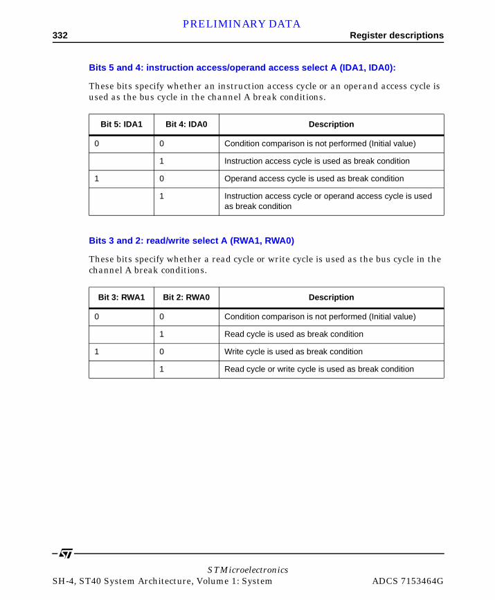
332 Register descriptionsPRELIMINARY DATA
Bits 5 and 4: instruction access/operand access select A (IDA1, IDA0):
These bits specify whether an instruction access cycle or an operand access cycle is used as the bus cycle in the channel A break conditions.
Bits 3 and 2: read/write select A (RWA1, RWA0)
These bits specify whether a read cycle or write cycle is used as the bus cycle in the channel A break conditions.
Bit 5: IDA1 Bit 4: IDA0 Description
0 0 Condition comparison is not performed (Initial value)
1 Instruction access cycle is used as break condition
1 0 Operand access cycle is used as break condition
1 Instruction access cycle or operand access cycle is used as break condition
Bit 3: RWA1 Bit 2: RWA0 Description
0 0 Condition comparison is not performed (Initial value)
1 Read cycle is used as break condition
1 0 Write cycle is used as break condition
1 Read cycle or write cycle is used as break condition
STMicroelectronicsSH-4, ST40 System Architecture, Volume 1: System ADCS 7153464G
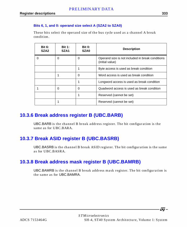
Register descriptions 333PRELIMINARY DATA
Bits 6, 1, and 0: operand size select A (SZA2 to SZA0)
These bits select the operand size of the bus cycle used as a channel A break condition.
10.3.6 Break address register B (UBC.BARB)
UBC.BARB is the channel B break address register. The bit configuration is the same as for UBC.BARA.
10.3.7 Break ASID register B (UBC.BASRB)
UBC.BASRB is the channel B break ASID register. The bit configuration is the same as for UBC.BASRA.
10.3.8 Break address mask register B (UBC.BAMRB)
UBC.BAMRB is the channel B break address mask register. The bit configuration is the same as for UBC.BAMRA.
Bit 6: SZA2
Bit 1: SZA1
Bit 0: SZA0
Description
0 0 0 Operand size is not included in break conditions(initial value)
1 Byte access is used as break condition
1 0 Word access is used as break condition
1 Longword access is used as break condition
1 0 0 Quadword access is used as break condition
1 Reserved (cannot be set)
1 Reserved (cannot be set)
STMicroelectronicsADCS 7153464G SH-4, ST40 System Architecture, Volume 1: System

334 Register descriptionsPRELIMINARY DATA
10.3.9 Break data register B (UBC.BDRB)
Break data register B (UBC.BDRB) is a 32-bit read/write register that specifies the data (bits 31 to 0) to be used in the channel B break conditions. UBC.BDRB is not initialized by a power-on reset or manual reset.
Bit 31 30 29 28 27 26 25 24
BDB31 BDB30 BDB29 BDB28 BDB27 BDB26 BDB25 BDB24
Initial value
- - - - - - - -
Type RW RW RW RW RW RW RW RW
Bit 23 22 21 20 19 18 17 16
BDB23 BDB22 BDB21 BDB20 BDB19 BDB18 BDB17 BDB16
Initial value
- - - - - - - -
RW RW RW RW RW RW RW RW RW
Bit 15 14 13 12 11 10 9 8
BDB15 BDB14 BDB13 BDB12 BDB11 BDB10 BDB9 BDB8
Initial value
- - - - - - - -
RW RW RW RW RW RW RW RW RW
Bit 7 6 5 4 3 2 1 0
BDB7 BDB6 BDB5 BDB4 BDB3 BDB2 BDB1 BDB0
Initial value
- - - - - - - -
RW RW RW RW RW RW RW RW RW
STMicroelectronicsSH-4, ST40 System Architecture, Volume 1: System ADCS 7153464G

Register descriptions 335PRELIMINARY DATA
Bits 31 to 0: break data B31 to B0 (BDB31 to BDB0):
These bits hold the data (bits 31 to 0) to be used in the channel B break conditions.
10.3.10 Break data mask register B (UBC.BDMRB)
Bit 31 30 29 28 27 26 25 24
BDMB31 BDMB30 BDMB29 BDMB28 BDMB27 BDMB26 BDMB25 BDMB24
Initial value
- - - - - - - -
Type RW RW RW RW RW RW RW RW
Bit 23 22 21 20 19 18 17 16
BDMB23 BDMB22 BDMB21 BDMB20 BDMB19 BDMB18 BDMB17 BDMB16
Initial value
- - - - - - - -
Type RW RW RW RW RW RW RW RW
Bit 15 14 13 12 11 10 9 8
BDMB15 BDMB14 BDMB13 BDMB12 BDMB11 BDMB10 BDMB9 BDMB8
Initial value
- - - - - - - -
Type RW RW RW RW RW RW RW RW
Bit 7 6 5 4 3 2 1 0
BDMB7 BDMB6 BDMB5 BDMB4 BDMB3 BDMB2 BDMB1 BDMB0
Initial value
- - - - - - - -
Type RW RW RW RW RW RW RW RW
STMicroelectronicsADCS 7153464G SH-4, ST40 System Architecture, Volume 1: System
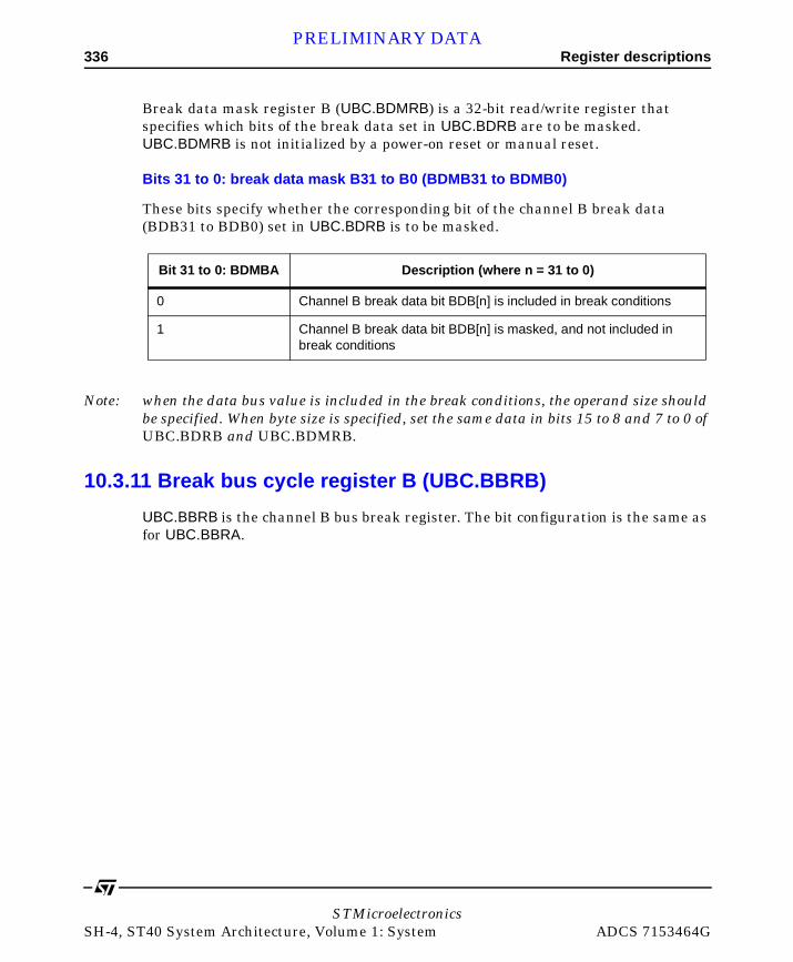
336 Register descriptionsPRELIMINARY DATA
Break data mask register B (UBC.BDMRB) is a 32-bit read/write register that specifies which bits of the break data set in UBC.BDRB are to be masked. UBC.BDMRB is not initialized by a power-on reset or manual reset.
Bits 31 to 0: break data mask B31 to B0 (BDMB31 to BDMB0)
These bits specify whether the corresponding bit of the channel B break data (BDB31 to BDB0) set in UBC.BDRB is to be masked.
Note: when the data bus value is included in the break conditions, the operand size should be specified. When byte size is specified, set the same data in bits 15 to 8 and 7 to 0 of UBC.BDRB and UBC.BDMRB.
10.3.11 Break bus cycle register B (UBC.BBRB)
UBC.BBRB is the channel B bus break register. The bit configuration is the same as for UBC.BBRA.
Bit 31 to 0: BDMBA Description (where n = 31 to 0)
0 Channel B break data bit BDB[n] is included in break conditions
1 Channel B break data bit BDB[n] is masked, and not included in break conditions
STMicroelectronicsSH-4, ST40 System Architecture, Volume 1: System ADCS 7153464G
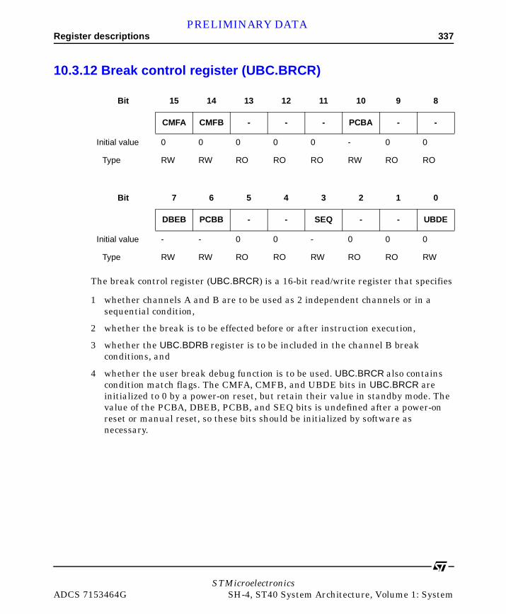
Register descriptions 337PRELIMINARY DATA
10.3.12 Break control register (UBC.BRCR)
The break control register (UBC.BRCR) is a 16-bit read/write register that specifies
1 whether channels A and B are to be used as 2 independent channels or in a sequential condition,
2 whether the break is to be effected before or after instruction execution,
3 whether the UBC.BDRB register is to be included in the channel B break conditions, and
4 whether the user break debug function is to be used. UBC.BRCR also contains condition match flags. The CMFA, CMFB, and UBDE bits in UBC.BRCR are initialized to 0 by a power-on reset, but retain their value in standby mode. The value of the PCBA, DBEB, PCBB, and SEQ bits is undefined after a power-on reset or manual reset, so these bits should be initialized by software as necessary.
Bit 15 14 13 12 11 10 9 8
CMFA CMFB - - - PCBA - -
Initial value 0 0 0 0 0 - 0 0
Type RW RW RO RO RO RW RO RO
Bit 7 6 5 4 3 2 1 0
DBEB PCBB - - SEQ - - UBDE
Initial value - - 0 0 - 0 0 0
Type RW RW RO RO RW RO RO RW
STMicroelectronicsADCS 7153464G SH-4, ST40 System Architecture, Volume 1: System

338 Register descriptionsPRELIMINARY DATA
Bit 15: condition match flag A (CMFA)
Set to 1 when a break condition set for channel A is satisfied. This flag is not cleared to 0 (to confirm that the flag is set again after once being set, it should be cleared with a write.)
Bit 14: condition match flag B (CMFB)
Set to 1 when a break condition set for channel B is satisfied. This flag is not cleared to 0 (to confirm that the flag is set again after once being set, it should be cleared with a write.)
Bits 13 to 11: reserved
These bits are always read as 0, and should only be written with 0.
Bit 10: instruction access break select A (PCBA)
Specifies whether a channel A instruction access cycle break is to be effected before or after the instruction is executed. This bit is not initialized by a power-on reset or manual reset.
Bit 15: CMFA Description
0 Channel A break condition is not matched (initial value)
1 Channel A break condition match has occurred
Bit 14: CMFB Description
0 Channel B break condition is not matched (initial value)
1 Channel B break condition match has occurred
Bit 10: PCBA Description
0 Channel A PC break is effected before instruction execution
1 Channel A PC break is effected after instruction execution
STMicroelectronicsSH-4, ST40 System Architecture, Volume 1: System ADCS 7153464G

Register descriptions 339PRELIMINARY DATA
Bits 9 and 8: reserved
These bits are always read as 0, and should only be written with 0.
Bit 7: data break enable B (DBEB)
Specifies whether the data bus condition is to be included in the channel B break conditions. This bit is not initialized by a power-on reset or manual reset.
Note: when the data bus is included in the break conditions, bits IDB1 to 0 in break bus cycle register B (UBC.BBRB) should be set to 10 or 11.
Bit 6: PC break select B (PCBB)
Specifies whether a channel B instruction access cycle break is to be effected before or after the instruction is executed. This bit is not initialized by a power-on reset or manual reset.
Bits 5 and 4: reserved
These bits are always read as 0, and should only be written with 0.
Bit 7: DBEB Description
0 Data bus condition is not included in channel B conditions
1 Data bus condition is included in channel B conditions
Bit 6: PCBB Description
0 Channel B PC break is effected before instruction execution
1 Channel B PC break is effected after instruction execution
STMicroelectronicsADCS 7153464G SH-4, ST40 System Architecture, Volume 1: System
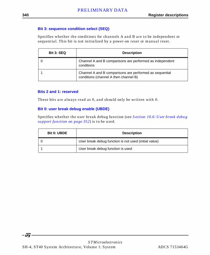
340 Register descriptionsPRELIMINARY DATA
Bit 3: sequence condition select (SEQ)
Specifies whether the conditions for channels A and B are to be independent or sequential. This bit is not initialized by a power-on reset or manual reset.
Bits 2 and 1: reserved
These bits are always read as 0, and should only be written with 0.
Bit 0: user break debug enable (UBDE)
Specifies whether the user break debug function (see Section 10.6: User break debug support function on page 352) is to be used.
Bit 3: SEQ Description
0 Channel A and B comparisons are performed as independent conditions
1 Channel A and B comparisons are performed as sequential conditions (channel A then channel B)
Bit 0: UBDE Description
0 User break debug function is not used (initial value)
1 User break debug function is used
STMicroelectronicsSH-4, ST40 System Architecture, Volume 1: System ADCS 7153464G

Operation 341PRELIMINARY DATA
10.4 Operation
10.4.1 Explanation of terms relating to accesses
An instruction access is an access that obtains an instruction. An operand access is any memory access for the purpose of instruction execution. For example, the access to address PC + dispx2 + 4 in the instruction MOV.W @ (disp, PC), Rn (an access very close to the program counter) is an operand access. The fetching of an instruction from the branch destination when a branch instruction is executed is also an instruction access. As the term “data” is used to distinguish data from an address, the term “operand access” is used in this section.
In the ST40, all operand accesses are treated as either read accesses or write accesses. The following instructions require special attention:
• PREF, OCBP, and OCBWB instructions: treated as read accesses,
• MOVCA and OCBI instructions: treated as write accesses,
• TAS instruction: treated as 1 read access and 1 write access.
The operand accesses for the PREF, OCBP, OCBWB, and OCBI instructions are accesses with no access data.
The ST40 handles all operand accesses as having a data size. The data size can be byte, word, longword, or quadword. The operand data size for the PREF, OCBP, OCBWB, MOVCA, and OCBI instructions is treated as longword.
10.4.2 Explanation of terms relating to instruction intervals
In this section, “1 (2, 3,...) instruction(s) after...”, as a measure of the distance between 2 instructions, is defined as follows. A branch is counted as an interval of 2 instructions.
STMicroelectronicsADCS 7153464G SH-4, ST40 System Architecture, Volume 1: System

342 OperationPRELIMINARY DATA
Example of sequence of instructions with no branch
Example of sequence of instructions with a branch
The example of a sequence of instructions with no branch should be applied when the branch destination of a delayed branch instruction is the instruction itself + 4.
10.4.3 User break operation sequence
The sequence of operations from setting of break conditions to user break exception handling is described below.
1 Specify pre- or post-execution breaking in the case of an instruction access, inclusion or exclusion of the data bus value in the break conditions in the case of an operand access, and use of independent or sequential channel A and channel B break conditions, in the break control register (UBC.BRCR).
2 Set the break addresses in the break address registers for each channel (UBC.BARA, UBC.BARB), the ASIDs corresponding to the break space in the break ASID registers (UBC.BASRA, UBC.BASRB), and the address and ASID masking methods in the break address mask registers (UBC.BAMRA, UBC.BAMRB).
100 Instruction A (0 instructions after instruction A)
102 Instruction B (1 instruction after instruction A)
104 Instruction [c](2 instructions after instruction A)
106 Instruction [d](3 instructions after instruction A)
100 Instruction A:BT/S L200 (0 instructions after instruction A)
102 Instruction B (1 instruction after instruction A, 0 instructions after instruction B)
L200 200 Instruction [c](3 instructions after instruction A, 2 instructions after instruction B)
202 Instruction [d](4 instructions after instruction A, 3 instructions after instruction B)
STMicroelectronicsSH-4, ST40 System Architecture, Volume 1: System ADCS 7153464G
Operation 343PRELIMINARY DATA
3 If the data bus value is to be included in the break conditions, also set the break data in the break data register (UBC.BDRB) and the data mask in the break data mask register (UBC.BDMRB).
4 Set the break bus conditions in the break bus cycle registers (UBC.BBRA, UBC.BBRB).
5 If either of the instruction access/operand access select group (IDA[n] and IDB[n] bits) or read/write select group (RWA[n] and RWB[n] bits) of the UBC.BBRA OR UBC.BBRB registers are set to 00, a user break interrupt is not generated on the corresponding channel.
6 Make the UBC.BBRA and UBC.BBRB settings after all other break-related register settings have been completed. If breaks are enabled with UBC.BBRA/UBC.BBRB while the break address, data, or mask register, or the break control register is in the initial state after a reset, a break may be generated inadvertently.
7 The operation when a break condition is satisfied depends on the BL bit (in the CPU’s SR register). When the BL bit is 0, exception handling is started and the condition match flag (CMFA, CMFB) for the respective channel is set for the matched condition. When the BL bit is 1, the condition match flag (CMFA, CMFB) for the respective channel is set for the matched condition but exception handling is not started.
The condition match flags (CMFA, CMFB) are set by a branch condition match, but are not reset. Therefore, a memory store instruction should be used on the UBC.BRCR register to clear the flags to 0. See Section 10.4.6: Condition match flag setting on page 346, for the exact setting conditions for the condition match flags.
8 When sequential condition mode has been selected, and the channel B condition is matched after the channel A condition has been matched, a break is effected at the instruction at which the channel B condition was matched. See Section 10.4.8: Contiguous A and B settings for sequential conditions on page 348, for the operation when the channel A condition match and channel B condition match occur close together. With sequential conditions, only the channel B condition match flag is set. When sequential condition mode has been selected, if it is wished to clear the channel A match when the channel A condition has been matched but the channel B condition has not yet been matched, this can be done by writing 0 to the SEQ bit in the UBC.BRCR register.
STMicroelectronicsADCS 7153464G SH-4, ST40 System Architecture, Volume 1: System

344 OperationPRELIMINARY DATA
10.4.4 Instruction access cycle break
1 When an instruction access, read or word setting is made in the break bus cycle register (UBC.BBRA, UBC.BBRB), an instruction access cycle can be used as a break condition. In this case, breaking before or after execution of the relevant instruction can be selected with the PCBA/PCBB bit in the break control register (UBC.BRCR). When an instruction access cycle is used as a break condition, clear the LSB of the break address registers (UBC.BARA, UBC.BARB) to 0. A break will not be generated if this bit is set to 1.
2 When a pre-execution break is specified, the break is effected when it is confirmed that the instruction is to be fetched and executed. Therefore, an overrun-fetched instruction (an instruction that is fetched but not executed when a branch or exception occurs) cannot be used in a break. However, if a TLB miss or TLB protection violation exception occurs at the time of the fetch of an instruction subject to a break, the break exception handling is carried out first. The instruction TLB exception handling is performed when the instruction is re- executed (see Exception Types and Priorities in the ST40 CPU Architecture Manual). Also, since a delayed branch instruction and the delay slot instruction are executed as a single instruction, if a pre-execution break is specified for a delay slot instruction, the break will be effected before execution of the delayed branch instruction. However, a pre-execution break cannot be specified for the delay slot instruction for an RTE instruction.
3 With a pre-execution break, the instruction set as a break condition is executed, then a break interrupt is generated before the next instruction is executed. When a post-execution break is set for a delayed branch instruction, the delay slot is executed and the break is effected before execution of the instruction at the branch destination (when the branch is made) or the instruction 2 instructions ahead of the branch instruction (when the branch is not made).
4 When an instruction access cycle is set for channel B, break data register B (UBC.BDRB) is ignored in judging whether there is an instruction access match. Therefore, a break condition specified by the DBEB bit in UBC.BRCR is not executed.
STMicroelectronicsSH-4, ST40 System Architecture, Volume 1: System ADCS 7153464G

Operation 345PRELIMINARY DATA
10.4.5 Operand access cycle break
1 In the case of an operand access cycle break, the bits included in address bus comparison vary as shown in Table 135 according to the data size specification in the break bus cycle register (UBC.BBRA, UBC.BBRB).
2 When data value is included in the break conditions in channel B, set the DBEB bit in the break control register (UBC.BRCR) to 1. In this case, break data register B (UBC.BDRB) and break data mask register B (UBC.BDMRB) settings are necessary in addition to the address condition. A user break interrupt is generated when all 3 conditions (address, ASID, and data) are matched. When a quadword access occurs, the 64-bit access data is divided into an upper 32 bits and lower 32 bits, and interpreted as two 32-bit data units. A break is generated if either of the 32-bit data units satisfies the data match condition.
Set the IDB1 and IDB0 bits in break bus cycle register B (UBC.BBRB) to 10 or 11. When byte data is specified, the same data should be set in the 2 bytes comprising bits 15 to 8 and bits 7 to 0 in break data register B (UBC.BDRB) and break data mask register B (UBC.BDMRB). When word or byte is set, bits 31 to 16 of UBC.BDRB and UBC.BDMRB are ignored.
3 When the DBEB bit in the break control register (UBC.BRCR) is set to 1, a break is not generated by an operand access with no access data (an operand access in a PREF, OCBP, OCBWB, or OCBI instruction).
Data size Address bits compared
Quadword (100) Address bits A31 to A3
Longword (011) Address bits A31 to A2
Word (010) Address bits A31 to A1
Byte (001) Address bits A31 to A0
Not included in condition (000) In quadword access, address bits A31 to A3
In longword access, address bits A31 to A2
In word access, address bits A31 to A1
In byte access, address bits A31 to A0
Table 135: Bits included in address bus comparison
STMicroelectronicsADCS 7153464G SH-4, ST40 System Architecture, Volume 1: System
346 OperationPRELIMINARY DATA
10.4.6 Condition match flag setting
Instruction access with post-execution condition, or operand access
The flag is set when execution of the instruction that causes the break is completed. As an exception to this, however, in the case of an instruction with more than 1 operand access the flag may be set on detection of the match condition alone, without waiting for execution of the instruction to be completed.
Example 1
Example 2
Instruction access with pre-execution condition
The flag is set when the break match condition is detected.
Example 1
Example 2
100 BT L200 (branch performed)
102 Instruction (operand access break on channel A): flag not set
110 FADD (FPU exception)
112 Instruction (operand access break on channel A): flag not set
110 Instruction (pre-execution break on channel A): flag set
112 Instruction (pre-execution break on channel B): flag not set
110 Instruction (pre-execution break on channel B, instruction access TLB miss): flag set
STMicroelectronicsSH-4, ST40 System Architecture, Volume 1: System ADCS 7153464G
Operation 347PRELIMINARY DATA
10.4.7 Program counter (PC) value saved
1 When instruction access (pre-execution) is set as a break condition, the program counter (PC) value saved to SPC in user break interrupt handling is the address of the instruction at which the break condition match occurred. In this case, a user break interrupt is generated and the fetched instruction is not executed.
2 When instruction access (post-execution) is set as a break condition, the program counter (PC) value saved to SPC in user break interrupt handling is the address of the instruction to be executed after the instruction at which the break condition match occurred. In this case, the fetched instruction is executed, and a user break interrupt is generated before execution of the next instruction.
3 When an instruction access (post-execution) break condition is set for a delayed branch instruction, the delay slot instruction is executed and a user break is effected before execution of the instruction at the branch destination (when the branch is made) or the instruction 2 instructions ahead of the branch instruction (when the branch is not made). In this case, the PC value saved to SPC is the address of the branch destination (when the branch is made) or the instruction following the delay slot instruction (when the branch is not made).
4 When operand access (address only) is set as a break condition, the address of the instruction to be executed after the instruction at which the condition match occurred is saved to SPC.
5 When operand access (address + data) is set as a break condition, execution of the instruction at which the condition match occurred is completed. A user break interrupt is generated before execution of instructions from 1 instruction later to 4 instructions later. It is not possible to specify at which instruction, from 1 later to 4 later, the interrupt will be generated. The start address of the instruction after the instruction for which execution is completed at the point at which user break interrupt handling is started is saved to SPC.
6 If an instruction between 1 instruction later and 4 instructions later causes another exception, control is performed as follows. Designating the exception caused by the break as exception 1, and the exception caused by an instruction between 1 instruction later and 4 instructions later as exception 2, the fact that memory updating and register updating that essentially cannot be performed by exception 2 cannot be performed is guaranteed irrespective of the existence of exception 1. The program counter value saved is the address of the first instruction for which execution is suppressed. Whether exception 1 or exception 2 is used for the exception jump destination and the value written to the exception register (EXPEVT, INTEVT) is not guaranteed. However, if exception 2 is from a source not synchronized with an instruction (external interrupt or
STMicroelectronicsADCS 7153464G SH-4, ST40 System Architecture, Volume 1: System

348 OperationPRELIMINARY DATA
peripheral module interrupt), exception 1 is used for the exception jump destination and the value written to the exception register (EXPEVT, INTEVT).
10.4.8 Contiguous A and B settings for sequential conditions
When channel A match and channel B match timings are close together, a sequential break may not be guaranteed. Rules relating to the guaranteed range are given below.
Instruction access matches on both channel A and channel B
Instruction access match on channel A, operand access match on channel B
Operand access match on channel A, instruction access match on channel B
Instruction B is 0 instructions after instruction A
Equivalent to setting the same address. Do not use this setting.
Instruction B is 1 instruction after instruction A
Sequential operation is not guaranteed.
Instruction B is 2 or more instructions after instruction A
Sequential operation is guaranteed.
Instruction B is 0 or 1 instruction after instruction A
Sequential operation is not guaranteed.
Instruction B is 2 or more instructions after instruction A
Sequential operation is guaranteed.
Instruction B is 0 to 3 instructions after instruction A
Sequential operation is not guaranteed.
Instruction B is 4 or more instructions after instruction A
Sequential operation is guaranteed.
STMicroelectronicsSH-4, ST40 System Architecture, Volume 1: System ADCS 7153464G

Operation 349PRELIMINARY DATA
Operand access matches on both channel A and channel B
Do not make a setting such that a single operand access will match the break conditions of both channel A and channel B. There are no other restrictions. For example, sequential operation is guaranteed even if 2 accesses within a single instruction match channel A and channel B conditions in turn.
STMicroelectronicsADCS 7153464G SH-4, ST40 System Architecture, Volume 1: System

350 Usage notesPRELIMINARY DATA
10.5 Usage notes 1 Do not execute a post-execution instruction access break for the SLEEP
instruction.
2 Do not make an operand access break setting between 1 and 3 instructions before a SLEEP instruction.
3 The value of the BL bit referenced in a user break exception depends on the break setting, as follows.
3.1 Pre-execution instruction access break: the BL bit value before the executed instruction is referenced.
3.2 Post-execution instruction access break: the OR of the BL bit values before and after the executed instruction is referenced.
3.3 Operand access break (address or data): the BL bit value after the executed instruction is referenced.
3.4 Instruction that modifies the BL bit: see Table 136.
3.5 RTE delay slot: the BL bit value before execution of a delay slot instruction is the same as the BL bit value before execution of an RTE instruction. The BL bit value after execution of a delay slot instruction is the same as the first BL bit value for the first instruction executed on returning by means of an RTE
SL.BLPre-execution instruction
access
Post-execution
instruction access
Pre-execution instruction
access
Post-execution
instruction access
Operand access
(address/data)
0 to 0 Accepted Accepted Accepted Accepted Accepted
1 to 0 Masked Masked Masked Masked Accepted
0 to 1 Accepted Masked Accepted Masked Masked
1 to 1 Masked Masked Masked Masked Masked
Table 136: Break setting for an instruction that modifies the BL bit
STMicroelectronicsSH-4, ST40 System Architecture, Volume 1: System ADCS 7153464G
Usage notes 351PRELIMINARY DATA
instruction (the same as the value of the BL bit in SSR before execution of the RTE instruction).
3.6 If an interrupt or exception is accepted with the BL bit cleared to 0, the value of the BL bit before execution of the first instruction of the exception handling routine is 1.
4 If channels A and B both match independently at virtually the same time, and, as a result, the SPC value is the same for both user break interrupts, only 1 user break interrupt is generated, but both the CMFA bit and the CMFB bit are set.
For example:
5 The PCBA or PCBB bit in UBC.BRCR is invalid for an instruction access break setting.
6 When the SEQ bit in UBC.BRCR is 1, the internal sequential break state is initialized by a channel B condition match.
For example:
7 In the event of contention between a re-execution type exception and a post-execution break in a multistep instruction, the re-execution type exception is generated. In this case, the CMF bit may or may not be set to 1 when the break condition occurs.
8 A post-execution break is classified as a completion type exception. Consequently, in the event of contention between a completion type exception and a post-execution break, the post-execution break is suppressed in accordance with the priorities of the 2 events. For example, in the case of contention between a TRAPA instruction and a post-execution break, the user break is suppressed. However, in this case, the CMF bit is set by the occurrence of the break condition.
110 Instruction (post-execution instruction break on channel A) → SPC = 112, CMFA = 1
112 Instruction (pre-execution instruction break on channel B) → SPC = 112, CMFB = 1
A → A → B (user break generated) B → (no break generated)
STMicroelectronicsADCS 7153464G SH-4, ST40 System Architecture, Volume 1: System

352 User break debug support functionPRELIMINARY DATA
10.6 User break debug support functionThe user break debug support function enables the processing used in the event of a user break exception to be changed. When a user break exception occurs, if the UBDE bit is set to 1 in the UBC.BRCR register, the DBR register value will be used as the branch destination address instead of [VBR + offset]. The value of R15 is saved in the SGR register regardless of the value of the UBDE bit in the UBC.BRCR register or the kind of exception event. A flowchart of the user break debug support function is shown in Figure 48.
Figure 48: User break debug support function flowchart
SPC ← PCSSR ← SR
SR.BL ← B'1
SR.MD ← B'1
SR.RB ← B'1
Exception/interruptgeneration
Exception Exception/interrupt/trap?
Trap
Interrupt
PC ← H'A0000000PC ← VBR + vector offset
Exception handler
Execute RTE instructionPC ← SPCSR ← SSR
SGR ← R15
TRA ← TRAPA (imm)
PC ← DBR
Debug program
R15 ← SGR(STC instruction)
Reset exception?
(BRCR.UBDE == 1) &&(user break exception)?
End of exceptionoperations
INTEVT ← interrupt codeEXPEVT ← exception code
YesNo
NoYes
Hardware operation
STMicroelectronicsSH-4, ST40 System Architecture, Volume 1: System ADCS 7153464G

Examples of use 353PRELIMINARY DATA
10.7 Examples of use
10.7.1 Instruction access cycle break condition settings
Independent channel A channel B mode: user break interrupt generated
Under these conditions a user break is generated after execution of the instruction at address 0x00000404 with ASID = 0x80, or before execution of an instruction at addresses 0x00008000 to 0x000083FE with ASID = 0x70.
Register settings
UBC.BASRA = 0x80,
UBC.BARA = 0x00000404,
UBC.BAMRA = 0x00,
UBC.BBRA = 0x0014,
UBC.BASRB = 0x70,
UBC.BARB = 0x00008010,
UBC.BAMRB = 0x01,
UBC.BBRB = 0x0014,
UBC.BDRB = 0x00000000,
UBC.BDMRB = 0x00000000,
UBC.BRCR = 0x0400.
Conditions set
Independent channel A channel B mode
Channel A
ASID: 0x80
Address: 0x00000404
Address mask: 0x00
STMicroelectronicsADCS 7153464G SH-4, ST40 System Architecture, Volume 1: System
354 Examples of usePRELIMINARY DATA
Bus cycle: instruction access (post-instruction- execution), read (operand size not included in conditions)
Channel B
ASID: 0x70
Address: 0x00008010
Address mask: 0x01
Data: 0x00000000
Data mask: 0x00000000
Bus cycle: instruction access (pre-instruction- execution), read (operand size not included in conditions)
Channel A channel B sequential mode: user break interrupt generated
Under these conditions the instruction at address 0x00037266 with ASID = 0x80 is executed, then a user break is generated before execution of the instruction at address 0x0003722E with ASID = 0x70.
Register settings
UBC.BASRA = 0x80,
UBC.BARA = 0x00037226,
UBC.BAMRA = 0x00,
UBC.BBRA = 0x0016,
UBC.BASRB = 0x70,
UBC.BARB = 0x0003722E,
UBC.BAMRB = 0x00,
UBC.BBRB = 0x0016,
UBC.BDRB = 0x00000000,
UBC.BDMRB = 0x00000000,
UBC.BRCR = 0x0008.
STMicroelectronicsSH-4, ST40 System Architecture, Volume 1: System ADCS 7153464G

Examples of use 355PRELIMINARY DATA
Conditions set
Channel A channel B sequential mode
Channel A
ASID: 0x80
Address: 0x00037226
Address mask: 0x00
Bus cycle: instruction access (pre-instruction- execution), read, word
Channel B
ASID: 0x70
Address: 0x0003722E
Address mask: 0x00
Data: 0x00000000
Data mask: 0x00000000
Bus cycle: instruction access (pre-instruction- execution), read, word
Independent channel A channel B mode: user break interrupts not generated
Under these conditions a user break interrupt is not generated on channel A since the instruction access is not a write cycle.
A user break interrupt is not generated on channel B since instruction access is performed on an even address.
Register settings
UBC.BASRA = 0x80
UBC.BARA = 0x00027128
UBC.BAMRA = 0x00
UBC.BBRA = 0x001A
UBC.BASRB = 0x70
UBC.BARB = 0x00031415
STMicroelectronicsADCS 7153464G SH-4, ST40 System Architecture, Volume 1: System
356 Examples of usePRELIMINARY DATA
UBC.BAMRB = 0x00
UBC.BBRB = 0x0014
UBC.BDRB = 0x00000000
UBC.BDMRB = 0x00000000
UBC.BRCR = 0x0000
Conditions set
Independent channel A and channel B mode
Channel A
ASID: 0x80
Address: 0x00027128
Address mask: 0x00
Bus cycle: CPU, instruction access (pre-instruction- execution), write, word
Channel B
ASID: 0x70
Address: 0x00031415
Address mask: 0x00
Data: 0x00000000
Data mask: 0x00000000
Bus cycle: CPU, instruction access (pre-instruction- execution), read (operand size not included in conditions)
10.7.2 Operand access cycle break condition settings
Under these conditions on channel A, a user break interrupt is generated in the event of a longword read at address 0x00123454, a word read at address 0x00123456, or a byte read at address 0x00123456, with ASID = 0x80.
On channel B, a user break interrupt is generated when 0xA512 is written by word access to any address from 0x000AB000 to 0x000ABFFE with ASID = 0x70.
STMicroelectronicsSH-4, ST40 System Architecture, Volume 1: System ADCS 7153464G

Examples of use 357PRELIMINARY DATA
Register settings
UBC.BASRA = 0x80
UBC.BARA = 0x00123456
UBC.BAMRA = 0x00
UBC.BBRA = 0x0024
UBC.BASRB = 0x70
UBC.BARB = 0x000ABCDE
UBC.BAMRB = 0x02
UBC.BBRB = 0x002A
UBC.BDRB = 0x0000A512
UBC.BDMRB = 0x00000000
UBC.BRCR = 0x0080
Conditions set
Independent channel A channel B mode
Channel A
ASID: 0x80
Address: 0x00123456
Address mask: 0x00
Bus cycle: operand access, read (operand size not included in conditions)
Channel B
ASID: 0x70
Address: 0x000ABCDE
Address mask: 0x02
Data: 0x0000A512
Data mask: 0x00000000
Bus cycle: operand access, write, word data break enabled
STMicroelectronicsADCS 7153464G SH-4, ST40 System Architecture, Volume 1: System

358 Examples of usePRELIMINARY DATA
10.7.3 User break controller stop function
This function stops the clock supplied to the user break controller and is used to minimize power dissipation when the chip is operating.
Note: If you use this function, you cannot use the user break controller.
10.7.4 Transition to user break controller stopped state
Setting the MSTP5 bit of the CPG.STBGR2 (inside the CPG) to 1 stops the clock supply and causes the user break controller to enter the stopped state. Follow steps 1 to 5 below to set the MSTP5 bit to 1 and enter the stopped state.
1 Initialize UBC.BBRA and UBC.BBRB to 0.
2 Initialize UBC.BBCR to 0.
3 Make a dummy read of UBC.BBCR.
4 Read CPG.STBCR2, then set the MSTP5 bit in the read data to 1 and write back.
5 Make 2 dummy reads of CPG.STBCR2.
Make sure that, if an exception or interrupt occurs while performing steps 1 to 5, you do not change the values of these registers in the exception handling routine.
Do not read or write the following registers while the user break controller clock is stopped:
• UBC.BARA,
• UBC.BAMRA,
• UBC.BBRA,
• UBC.BARB,
• UBC.BAMRB,
• UBC.BBRB,
• UBC.BDRB,
• UBC.BDMRB,
• UBC.BRCR.
If these registers are read or written, the value cannot be guaranteed.
STMicroelectronicsSH-4, ST40 System Architecture, Volume 1: System ADCS 7153464G
Examples of use 359PRELIMINARY DATA
10.7.5 Cancelling the user break controller stopped state
The clock supply can be restarted by setting the CPG.MSTP5 bit of STBCR2 (inside the CPG) to 0. The user break controller can then be operated again. Follow steps 6 and 7 below to clear the MSTP5 bit to 0 to cancel the stopped state. This is similar to the transition to the stopped state.
6 Read CPG.STBCR2, then clear the MSTP5 bit in the read data to 0 and write the modified data back.
7 Make 2 dummy reads of CPG.STBGR2.
As with the transition to the stopped state, if an exception or interrupt occurs while processing steps 6 and 7, make sure that the values in these registers are not changed in the exception handling routine.
10.7.6 Examples of stopping and restarting the user break controller
The following are example programs:
; Transition to user break controller stopped state; (1)Initialize BBRA and BBRB to 0.
mov #0, R0mov.l#BBRA, R1mov.w R0, @R1mov.l#BBRB, R1mov.w R0, @R1
; (2)Initialize BBCR to 0.mov.l #BBCR, R1mov.w R0, @R1
; (3)Dummy read BRCR.mov.w R1, R0
; (4)Read STBCR2, then set MSTP5 bit in the read data to 1 and write
it backmov.l #STBCR2, R1mov.b @R0, R1or #H’1, R0mov.bR0, @R1
; (5)Twice dummy read STBCR2.mov.b @R1, R0mov.b @R1, R0
STMicroelectronicsADCS 7153464G SH-4, ST40 System Architecture, Volume 1: System
360 Examples of usePRELIMINARY DATA
; Canceling user break controller stopped state; (6)Read STBCR2, then clear MSTP5 bit in the read data to 0 and write
it backmov.l #STBCR2, R1mov.b @R1, R0
and #H’FE, R0mov.b R0, @R1
; (7)Twice dummy read STBGR2.mov.b@R1, R0mov.b@R1, R0
STMicroelectronicsSH-4, ST40 System Architecture, Volume 1: System ADCS 7153464G

PRELIMINARY DATA
STMicroelectroniADCS 7153464G SH-4, ST40 S
11
User debug interface (UDI) 11.1 Overview11.1.1 Features
The user debug interface (UDI) is a serial input/output interface conforming to JTAG, IEEE 1149.1, and IEEE Standard Test Access Port and Boundary- Scan Architecture. The ST40’s UDI supports boundary-scan, and is used for emulator connection. The functions of this interface should not be used when using an emulator. Refer to the emulator manual for the method of connecting the emulator. The UDI uses 6 pins (DCK, TMS, TDI, TDO, NOT_TRST, and NOT_ASEBRK/BRKACK). The pin functions and serial transfer protocol conform to the JTAG specifications.
11.1.2 Block diagram
Figure 49 shows a block diagram of the UDI. The TAP (test access port) controller and control registers are reset independently of the chip reset pin by driving the NOT_TRST pin low or setting TMS to 1 and applying DCK for at least 5 clock cycles. The other circuits are reset and initialized in an ordinary reset. The UDI circuit has 6 internal registers: SDBPR, SDBSR, SDIR, SDDRH, and SDDRL (these last 2 together designated SDDR) and SDINT. The SDBPR register supports the JTAG bypass mode, SDBSR is a shift register forming a JTAG boundary scan, SDIR is the command register, SDDR is the data register and SDINT is the UDI interrupt register. SDIR can be accessed directly from the TDI and TDO pins.
csystem Architecture, Volume 1: System

362 OverviewPRELIMINARY DATA
Figure 49: Block diagram of UDI circuit
SDIR
SDDRH
SDDRL
SDBPR
MUX
TCK
/BRKACK
TMS
TDI
TDO
SDINT
Interrupt/resetetc.
TAPcontroller
Breakcontrol
Decoder
Shi
ft re
gist
er
SD
BS
R
Per
iphe
ral m
odul
e bu
s
DCK
STMicroelectronicsSH-4, ST40 System Architecture, Volume 1: System ADCS 7153464G
Overview 363PRELIMINARY DATA
11.1.3 Pin configuration
Table 137 shows the UDI pin configuration.
Pin name Description I/O FunctionWhen not
used
DCK Clock pin Input Same as the JTAG serial clock input pin (TCK). Data is transferred from data input pin TDI to the UDI circuit, and data is read from data output pin TDO, in synchronization with this signal.
OpenA
TMS Mode pin Input The mode select input pin. Changing this signal in synchronization with DCK determines the meaning of the data input from TDI. The protocol conforms to the JTAG (IEEE Std 1149.1) specification.
OpenA
NOT_TRST Reset pin Input The input pin that resets the UDI. This signal is received asynchronously with respect to DCK, and effects a reset of the JTAG interface circuit when low. NOT_TRST must be driven low for a certain period when powering on, regardless of whether or not JTAG is used. This differs from the IEEE specification.
Fix at groundB
TDI Data input pin
Input The data input pin. Data is sent to the UDI circuit by changing this signal in synchronization with DCK.
OpenA
TDO Data output pin
Output The data output pin. Data is sent to the UDI circuit by reading this signal in synchronization with DCK.
OpenA
NOT_ASEBRK/BRKACK
Emulator pin Input/output
Dedicated emulator pin OpenA
Table 137: UDI pins
A. Pulled up inside the chip. When designing a board that allows use of an emulator, or when using interrupts and resets via the UDI, there is no problem in connecting a pull-up resistance externally.
STMicroelectronicsADCS 7153464G SH-4, ST40 System Architecture, Volume 1: System
364 OverviewPRELIMINARY DATA
The maximum frequency of DCK (TMS, TDI, TDO) is 20 MHz. Make the DCK or ST40 CPG setting so that the DCK frequency is lower than that of the ST40’s on-chip peripheral module clock.
11.1.4 Register configuration
Table 138 shows the UDI registers. Except for SDBPR and SDBSR, these registers are mapped in the control register space and can be referenced by the CPU.
B. When designing a board that enables the use of an emulator, or when using interrupts and resets via the UDI, drive NOT_TRST low for a period overlapping NOT_RESET at power-on, and also provide for control by NOT_TRST alone.
Register name
Description Initial valueA
CPU side
TypeP4
addressArea 7
addressAccess
size
UDI.SDIR Instruction register,see Section 11.2.1: Instruction register (SDIR) on page 367
0xFFFFFFFD
Fixed valuesBRO 0xFFF00000 0x1FF00000 16
UDI.SDDR/SDDRH
Data register H,see Section 11.2.2: Data register (SDDR) on page 370
Undefined RW 0xFFF00008 0x1FF00008 32/16
UDI.SDDRL Data register L,see Section 11.2.2: Data register (SDDR) on page 370
Undefined RW 0xFFF0000A 0x1FF0000A 16
Table 138: UDI registers on CPU side
STMicroelectronicsSH-4, ST40 System Architecture, Volume 1: System ADCS 7153464G

Overview 365PRELIMINARY DATA
UDI.SDBPR Bypass register,see Section 11.2.3: Bypass register (SDBPR) on page 371
Undefined - - - -
UDI.SDINT Interrupt factor register,see Section 11.2.4: Interrupt factor register (SDINT) on page 371
0x00000000 RW 0xFFF00014 0x1FF00014 18
UDI.SDBSR Boundary scan registersee Section 11.2.5: Boundary scan register (SDBSR) on page 372
Undefined - - - -
A. Initialized when the NOT_TRST pin goes low or when the TAP is in the test-logic-reset state.
B. The value read from UDI is fixed (0xFFFF FFFD)
Register name
Description Initial valueA
CPU side
TypeP4
addressArea 7
addressAccess
size
Table 138: UDI registers on CPU side
STMicroelectronicsADCS 7153464G SH-4, ST40 System Architecture, Volume 1: System

366 OverviewPRELIMINARY DATA
Register name
Description Initial valueAUDI side
Type Access size
UDI.SDIR Instruction register, see Section 11.2.1: Instruction register (SDIR) on page 367
0xFFFFFFFD
Fixed valuesBRW 16
UDI.SDDR/SDDRH
Data register H, see Section 11.2.2: Data register (SDDR) on page 370
Undefined - 32
UDI.SDDRL Data register L, see Section 11.2.2: Data register (SDDR) on page 370
Undefined - -
UDI.SDBPR Bypass register, see Section 11.2.3: Bypass register (SDBPR) on page 371
Undefined RW 1
UDI.SDINT Interrupt factor register, see Section 11.2.4: Interrupt factor register (SDINT) on page 371
0x00000000 WOC 32
UDI.SDBSR Boundary scan register see Section 11.2.5: Boundary scan register (SDBSR) on page 372
Undefined - -
Table 139: UDI registers on UDI side
A. Initialized when the NOT_TRST pin goes low or when the TAP is in the test-logic-reset state.
B. The value read from UDI is fixed (0xFFFF FFFD)
C. 1 can be written to the LSB using the UDI interrupt command.
STMicroelectronicsSH-4, ST40 System Architecture, Volume 1: System ADCS 7153464G
Register descriptions 367PRELIMINARY DATA
11.2 Register descriptions
11.2.1 Instruction register (SDIR)
The instruction register (SDIR) is a 16-bit register that can only be read by the CPU. In the initial state, bypass mode is set. The value (command) is set from the serial input pin (TDI). SDIR is initialized by the NOT_TRST pin or in the TAP test-logic-reset state. When this register is written to from the UDI, writing is possible regardless of the CPU mode. Operation is undefined if a reserved command is set in this register.
Bits 15 to 8:
Bit 15 14 13 12 11 10 9 8
TI7 TI6 TI5 TI4 T13 T12 T11 T10
Initial value 1 1 1 1 1 1 1 1
RW RO RO RO RO RO RO RO RO
Bit 7 6 5 4 3 2 1 0
- - - - - - - -
Initial value 1 1 1 1 1 1 1 1
RW RO RO RO RO RO RO RO RO
Bit 15:T17
Bit 14:T16
Bit 13:T15
Bit 12:T14
Bit 11: TI3
Bit 10: TI2
Bit 9: TI1
Bit 8: TI0
Description
0 0 0 0 0 0 0 0 EXTEST
0 0 0 0 0 1 0 0 SAMPLE/PRELOAD
0 1 1 0 - - - - UDI reset negate
0 1 1 1 - - - - UDI reset assert
STMicroelectronicsADCS 7153464G SH-4, ST40 System Architecture, Volume 1: System

368 Register descriptionsPRELIMINARY DATA
1 0 1 - - - - - UDI interrupt
1 1 1 1 1 1 1 1 Bypass mode (initial value)
Other than above Reserved
Bit 15:T17
Bit 14:T16
Bit 13:T15
Bit 12:T14
Bit 11: TI3
Bit 10: TI2
Bit 9: TI1
Bit 8: TI0
Description
STMicroelectronicsSH-4, ST40 System Architecture, Volume 1: System ADCS 7153464G
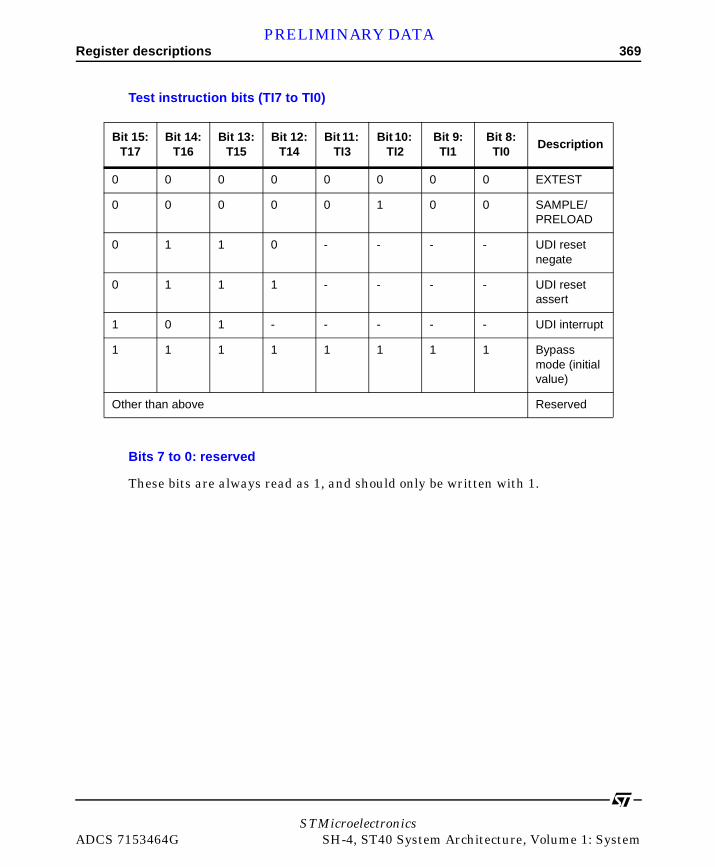
Register descriptions 369PRELIMINARY DATA
Test instruction bits (TI7 to TI0)
Bits 7 to 0: reserved
These bits are always read as 1, and should only be written with 1.
Bit 15:T17
Bit 14:T16
Bit 13:T15
Bit 12:T14
Bit 11: TI3
Bit 10: TI2
Bit 9: TI1
Bit 8: TI0
Description
0 0 0 0 0 0 0 0 EXTEST
0 0 0 0 0 1 0 0 SAMPLE/PRELOAD
0 1 1 0 - - - - UDI reset negate
0 1 1 1 - - - - UDI reset assert
1 0 1 - - - - - UDI interrupt
1 1 1 1 1 1 1 1 Bypass mode (initial value)
Other than above Reserved
STMicroelectronicsADCS 7153464G SH-4, ST40 System Architecture, Volume 1: System
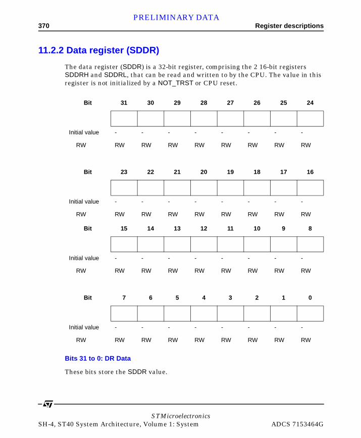
370 Register descriptionsPRELIMINARY DATA
11.2.2 Data register (SDDR)
The data register (SDDR) is a 32-bit register, comprising the 2 16-bit registers SDDRH and SDDRL, that can be read and written to by the CPU. The value in this register is not initialized by a NOT_TRST or CPU reset.
Bits 31 to 0: DR Data
These bits store the SDDR value.
Bit 31 30 29 28 27 26 25 24
Initial value - - - - - - - -
RW RW RW RW RW RW RW RW RW
Bit 23 22 21 20 19 18 17 16
Initial value - - - - - - - -
RW RW RW RW RW RW RW RW RW
Bit 15 14 13 12 11 10 9 8
Initial value - - - - - - - -
RW RW RW RW RW RW RW RW RW
Bit 7 6 5 4 3 2 1 0
Initial value - - - - - - - -
RW RW RW RW RW RW RW RW RW
STMicroelectronicsSH-4, ST40 System Architecture, Volume 1: System ADCS 7153464G
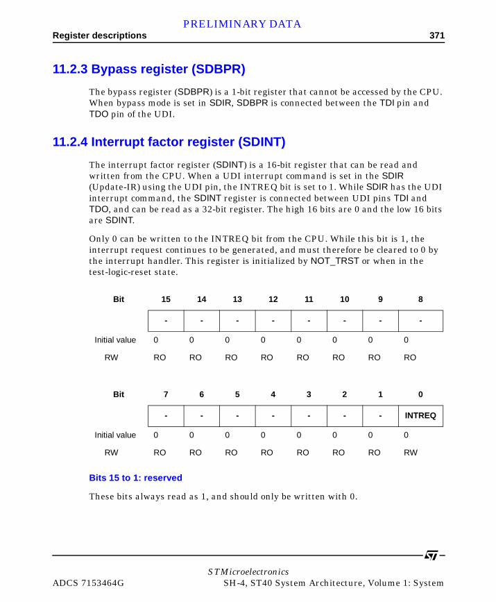
Register descriptions 371PRELIMINARY DATA
11.2.3 Bypass register (SDBPR)
The bypass register (SDBPR) is a 1-bit register that cannot be accessed by the CPU. When bypass mode is set in SDIR, SDBPR is connected between the TDI pin and TDO pin of the UDI.
11.2.4 Interrupt factor register (SDINT)
The interrupt factor register (SDINT) is a 16-bit register that can be read and written from the CPU. When a UDI interrupt command is set in the SDIR (Update-IR) using the UDI pin, the INTREQ bit is set to 1. While SDIR has the UDI interrupt command, the SDINT register is connected between UDI pins TDI and TDO, and can be read as a 32-bit register. The high 16 bits are 0 and the low 16 bits are SDINT.
Only 0 can be written to the INTREQ bit from the CPU. While this bit is 1, the interrupt request continues to be generated, and must therefore be cleared to 0 by the interrupt handler. This register is initialized by NOT_TRST or when in the test-logic-reset state.
Bits 15 to 1: reserved
These bits always read as 1, and should only be written with 0.
Bit 15 14 13 12 11 10 9 8
- - - - - - - -
Initial value 0 0 0 0 0 0 0 0
RW RO RO RO RO RO RO RO RO
Bit 7 6 5 4 3 2 1 0
- - - - - - - INTREQ
Initial value 0 0 0 0 0 0 0 0
RW RO RO RO RO RO RO RO RW
STMicroelectronicsADCS 7153464G SH-4, ST40 System Architecture, Volume 1: System

372 OperationPRELIMINARY DATA
Bit 0: interrupt request bit (INTREQ)
Shows the existence of an interrupt request from the UDI interrupt command. The interrupt request can be cleared by writing 0 to this bit from the CPU. When 1 is written to this bit, the existing value is retained.
11.2.5 Boundary scan register (SDBSR)
The boundary scan register (SDBSR) is a shift register on the pad for controlling the chip’s I/O pins. Using the EXTEST and SAMPLE/PRELOAD commands, it can perform a JTAG (IEEE Std 1149.1)-compatible boundary scan test.
11.3 Operation
11.3.1 TAP control
Figure 50 shows the internal states of the TAP control circuit. These conform to the state transitions specified by JTAG.
• The transition condition is the TMS value at the rising edge of DCK.
• The TDI value is sampled at the rising edge of DCK, and shifted at the falling edge.
• The TDO value changes at the falling edge of DCK. When not in the Shift-DR or Shift-IR state, TDO is in the high-impedance state.
• In a transition to NOT_TRST = 0, a transition is made to the Test-Logic-Reset state asynchronously with respect to DCK.
STMicroelectronicsSH-4, ST40 System Architecture, Volume 1: System ADCS 7153464G

Operation 373PRELIMINARY DATA
11.3.2 UDI reset
A power-on reset is effected by an SDIR command. A reset is effected by sending a UDI reset assert command, and then sending a UDI reset negate command, from the UDI pin (see Figure 51). The interval required between the UDI reset assert command and the UDI reset negate command is the same as the length of time the reset pin is held low in order to effect a power-on reset.
Figure 50: TAP control state transition diagram
1
0
0
0
Run-Test/Idle Select-DR-Scan
Capture-DR
Shift-DR
Exit1-DR
Pause-DR
Exit2-DR
Update-DR
Test-Logic-Reset
0
1 1
1
0
0
1
0
1
1
1
1 0
0
0
0
Select-IR-Scan
Capture-IR
Shift-IR
Exit1-IR
Pause-IR
Exit2-IR
Update-IR
1
1
0
0
1
0
1
1
1
1 0
0
STMicroelectronicsADCS 7153464G SH-4, ST40 System Architecture, Volume 1: System
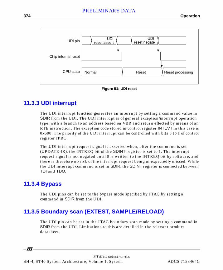
374 OperationPRELIMINARY DATA
11.3.3 UDI interrupt
The UDI interrupt function generates an interrupt by setting a command value in SDIR from the UDI. The UDI interrupt is of general exception/interrupt operation type, with a branch to an address based on VBR and return effected by means of an RTE instruction. The exception code stored in control register INTEVT in this case is 0x600. The priority of the UDI interrupt can be controlled with bits 3 to 1 of control register IPRC.
The UDI interrupt request signal is asserted when, after the command is set (UPDATE-IR), the INTREQ bit of the SDINT register is set to 1. The interrupt request signal is not negated until 0 is written to the INTREQ bit by software, and there is therefore no risk of the interrupt request being unexpectedly missed. While the UDI interrupt command is set in SDIR, the SDINT register is connected between TDI and TDO.
11.3.4 Bypass
The UDI pins can be set to the bypass mode specified by JTAG by setting a command in SDIR from the UDI.
11.3.5 Boundary scan (EXTEST, SAMPLE/RELOAD)
The UDI pin can be set in the JTAG boundary scan mode by setting a command in SDIR from the UDI. Limitations to this are detailed in the relevant product datasheet.
Figure 51: UDI reset
Hitachi-UDI pin
Chip internal reset
CPU state
Hitachi-UDIreset assert
Normal
Hitachi-UDIreset negate
Reset processingReset
STMicroelectronicsSH-4, ST40 System Architecture, Volume 1: System ADCS 7153464G

Usage notes 375PRELIMINARY DATA
11.4 Usage notes
11.4.1 SDIR command
Once an SDIR command has been set, it remains unchanged until initialization by asserting NOT_TRST or placing the TAP in the test-logic-reset state, or until another command (other than a UDI interrupt command) is written from the UDI.
11.4.2 SDIR commands in sleep mode
Sleep mode is cleared by a UDI interrupt or UDI reset, and these exception requests are accepted in this mode. In standby mode, neither a UDI interrupt nor a UDI reset is accepted.]
11.4.3 Emulator
The UDI is used for emulator connection. Therefore, UDI functions cannot be used when an emulator is used.
STMicroelectronicsADCS 7153464G SH-4, ST40 System Architecture, Volume 1: System

376 Usage notesPRELIMINARY DATA
STMicroelectronicsSH-4, ST40 System Architecture, Volume 1: System ADCS 7153464G
PRELIMINARY DATA
STMicroelectroniADCS 7153464G SH-4, ST40 S
12
Advanced userdebugger (AUD) 12.1 OverviewThe advanced user debugger (AUD) provides the function to support debugging of user programs. This function traces such events as branch and memory access that occur when a program is executed and outputs them.
12.1.1 Features
Features of the AUD are as follows:
• 6 input/output pins,
• memory mapped control and status register,
• branch tracing function: tracing of branch destination and branch source addresses,
• window data tracing function: support of A and B 2-channel windows,
- for tracing addresses for CPU memory accesses made in the range and their data,
- support of 8-, 16-, 32- and 64-bit data lengths,
• for outputting address differential information by small bit count,
• incorporation of 8-level FIFO,
• full trade mode: for outputting all traced data
• real-time trace mode: for obtaining traced data in real-time,
• AUD output clock ratio select function: support of 1, 1/2, 1/4 and 1/8 CPU clock ratios. ,
csystem Architecture, Volume 1: System

378 OverviewPRELIMINARY DATA
12.1.2 Block diagram
Figure 52 shows a block diagram of the AUD.
Figure 52: Block diagram of AUD
FPU Store BUS
CPU Store BUS
CPU Branch Trace
CPU Address BUS
FPUCPU
32bit
32bit
32bit
64bit
AUCSR
AUWASR
AUWAER
AUWBSR
AUWBER
AUD
Comparator
FIFO
Sync logic & State machine
AUDCK
AUDATA3-0 4
1
AUDSYNC1
PIN
Load2 BUS
Load1 BUS 32bit
32bit
STMicroelectronicsSH-4, ST40 System Architecture, Volume 1: System ADCS 7153464G
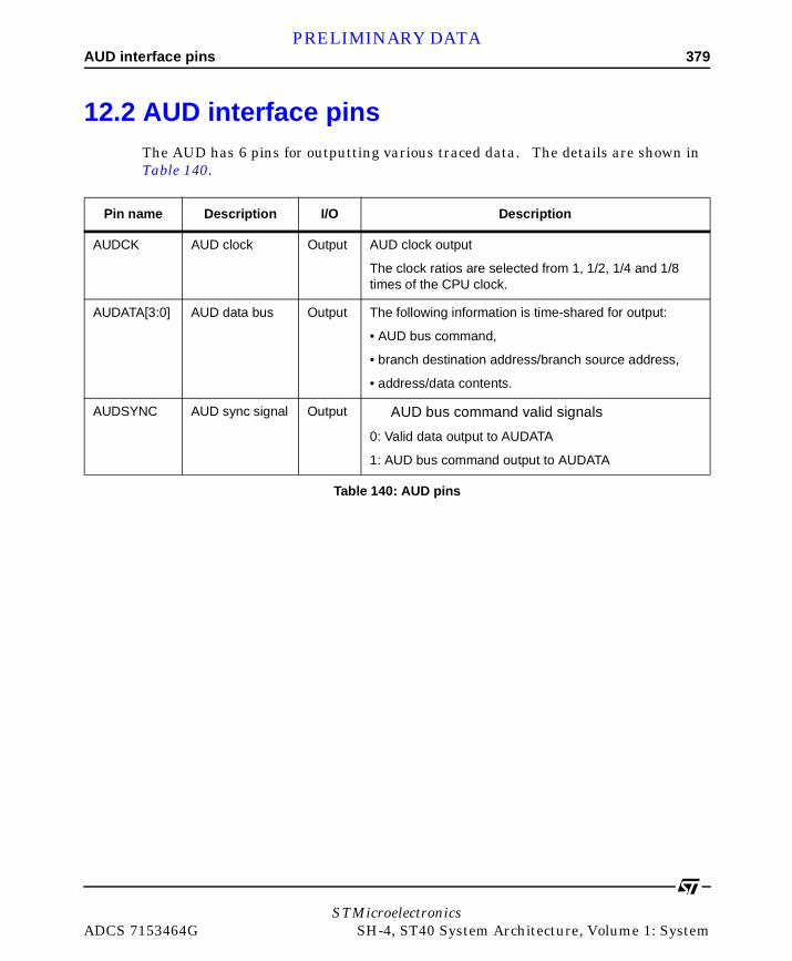
AUD interface pins 379PRELIMINARY DATA
12.2 AUD interface pinsThe AUD has 6 pins for outputting various traced data. The details are shown in Table 140.
Pin name Description I/O Description
AUDCK AUD clock Output AUD clock output
The clock ratios are selected from 1, 1/2, 1/4 and 1/8 times of the CPU clock.
AUDATA[3:0] AUD data bus Output The following information is time-shared for output:
• AUD bus command,
• branch destination address/branch source address,
• address/data contents.
AUDSYNC AUD sync signal Output AUD bus command valid signals
0: Valid data output to AUDATA
1: AUD bus command output to AUDATA
Table 140: AUD pins
STMicroelectronicsADCS 7153464G SH-4, ST40 System Architecture, Volume 1: System
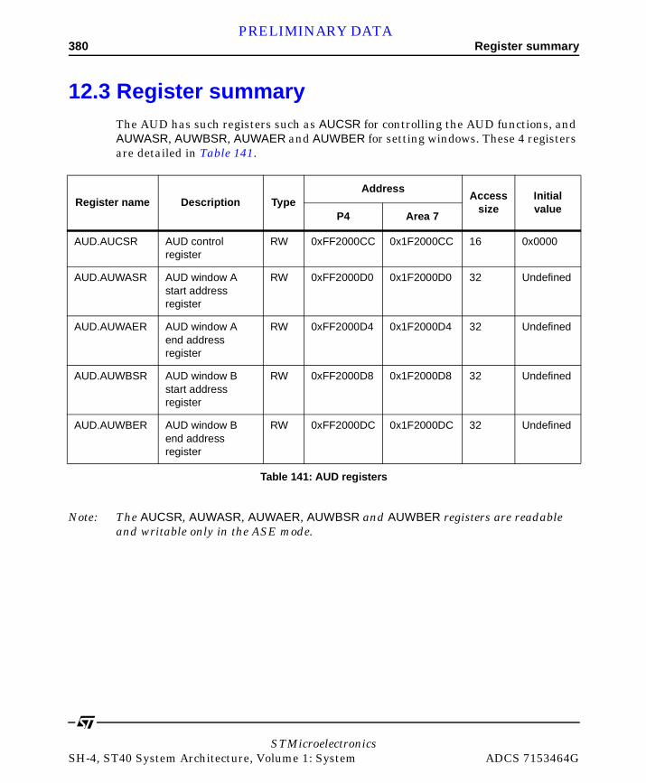
380 Register summaryPRELIMINARY DATA
12.3 Register summaryThe AUD has such registers such as AUCSR for controlling the AUD functions, and AUWASR, AUWBSR, AUWAER and AUWBER for setting windows. These 4 registers are detailed in Table 141.
Note: The AUCSR, AUWASR, AUWAER, AUWBSR and AUWBER registers are readable and writable only in the ASE mode.
Register name Description TypeAddress
Access size
Initial value
P4 Area 7
AUD.AUCSR AUD control register
RW 0xFF2000CC 0x1F2000CC 16 0x0000
AUD.AUWASR AUD window A start address register
RW 0xFF2000D0 0x1F2000D0 32 Undefined
AUD.AUWAER AUD window A end address register
RW 0xFF2000D4 0x1F2000D4 32 Undefined
AUD.AUWBSR AUD window B start address register
RW 0xFF2000D8 0x1F2000D8 32 Undefined
AUD.AUWBER AUD window B end address register
RW 0xFF2000DC 0x1F2000DC 32 Undefined
Table 141: AUD registers
STMicroelectronicsSH-4, ST40 System Architecture, Volume 1: System ADCS 7153464G
PRELIMINARY DATA
STMicroelectroniADCS 7153464G SH-4, ST40 S
13
ASE hardware break controller 13.1 OverviewThe ASE hardware break controller is partly responsible for emulation functions. When break conditions are set, the controller generates an ASE hardware break interrupt in response to the content of the CPU bus cycle. This function facilitates the creation of a self-monitoring debugger.
13.1.1 Features
The ASE hardware break controller has the following features:
• 4 channels (S, T, U, and V),
• conditions set independently for the individual channels, or ASE hardware break interrupts can be requested with sequential conditions (sequential settings: channel U → channel V, channel T → channel U → channel V, channel S → channel T → channel U → channel V),
• 32-bit logical address and ASID compare:
- address compare: compare all bits, mask lower 10 bits, mask lower 12 bits, mask lower 16 bits, mask lower 20 bits, mask all bits,
- ASID compare: compare all bits, mask all bits,
• data: channel V only, 32-bit maskable,
• bus cycle: instruction access, operand access
• read/write
csystem Architecture, Volume 1: System
382 OverviewPRELIMINARY DATA
• data size: byte, word, longword, quadword
• break on instruction access cycle can be set for either before or after instruction execution.
13.1.2 Differences between the user break controller and ASE hardware break controller
1 The user break controller has 2 channels (A and B); the ASE hardware break controller has 4 channels (S, T, U, and V) which are completely independent from A and B.
2 The branch is to address VBR + 0x00000100 or DBR on a user break, and address 0xFC000000 on an ASE hardware break.
3 There is a change to privileged mode on a user break; the change is to ASE mode on an ASE hardware break.
STMicroelectronicsSH-4, ST40 System Architecture, Volume 1: System ADCS 7153464G

Overview 383PRELIMINARY DATA
13.1.3 Block diagram
Figure 53 illustrates the block diagram of the User break controller and the ASE hardware break controller.
Figure 53: Block diagram of user break controller and ASE hardware break controller
Access comparator
Channel A
Address comparator
BBRA
BARA
BASRA*
BAMRA
Access comparator
Channel B
Address comparator
BBRB
BARB
BASRB*
BAMRB
Data comparator
BDRB
BDMRB
Access comparator
Channels S,T,U
Address comparator
BBRS
BARS
BASRS*
BAMRS
Access comparator
Channel V
Address comparator
BBRV
BARV
BASRV*
BAMRV
Data comparator
BDRV
BDMRV
Control
BRCR
BRCRA
BRCRS
IOBAR
IOBDR
ASEEVT
Break interrupt request
Access control
Local address
bus Data bus
STMicroelectronicsADCS 7153464G SH-4, ST40 System Architecture, Volume 1: System

384 Register summaryPRELIMINARY DATA
13.2 Register summaryTable 142 shows the control register configuration of the ASE hardware break controller. The BRCR is the same as that listed for the user break controller.
Register name Description
ASE.BARS Break address register S
ASE.BAMRS Break address mask register S
ASE.BBRS Break bus cycle register S
ASE.BASRS Break ASID register SA
ASE.BART Break address register T
ASE.BAMRT Break address mask register T
ASE.BBRT Break bus cycle register T
ASE.BASRT Break ASID register TA
ASE.BARU Break address register U
ASE.BAMRU Break address mask register U
ASE.BBRU Break bus cycle register U
ASE.BASRU Break ASID register UA
ASE.BARV Break address register V
ASE.BAMRV Break address mask register V
ASE.BBRV Break bus cycle register V
ASE.BASRV Break ASID register VA
ASE.BDRV Break data register V
ASE.BDMRV Break data mask register V
ASE.BRCRA ASE Break control register
Table 142: ASE hardware break controller registers
STMicroelectronicsSH-4, ST40 System Architecture, Volume 1: System ADCS 7153464G
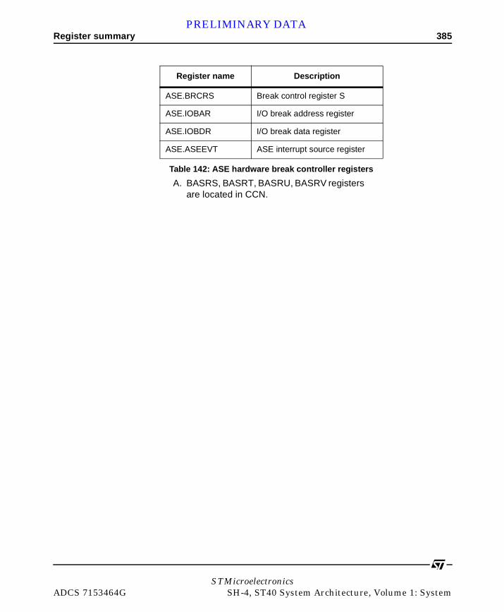
Register summary 385PRELIMINARY DATA
ASE.BRCRS Break control register S
ASE.IOBAR I/O break address register
ASE.IOBDR I/O break data register
ASE.ASEEVT ASE interrupt source register
A. BASRS, BASRT, BASRU, BASRV registers are located in CCN.
Register name Description
Table 142: ASE hardware break controller registers
STMicroelectronicsADCS 7153464G SH-4, ST40 System Architecture, Volume 1: System
386 Register summaryPRELIMINARY DATA
STMicroelectronicsSH-4, ST40 System Architecture, Volume 1: System ADCS 7153464G
PRELIMINARY DATA
Appendices
STMicroelectronicsADCS 7153464G SH-4, ST40 System Architecture, Volume 1: System
388PRELIMINARY DATA
STMicroelectronicsSH-4, ST40 System Architecture, Volume 1: System ADCS 7153464G
PRELIMINARY DATA
STMicroelectroniADCS 7153464G SH-4, ST40 S
A
ST40 system architectural conventions A.1 IntroductionThe ST40 follows architectural conventions which present a consistent interface to ST40 modules.
Note: since systems are typically a mixture of legacy blocks and new IP, in places it is not practical to follow these convention strictly. Nonetheless this appendix documents some of those conventions and describes the semantics of the formats used in this document.
A.1.1 Memory blocks
There are three types of memory blocks:
• control blocks (CB),
• data blocks (DB),
• undefined blocks (UB).
A control block contains a collection of memory-mapped registers holding a variety of status and control information for an ST40 module. There is a 1-to-1 association between ST40 modules and control blocks. Most control blocks contain a Version Control Register (VCR). A VCR identifies the module associated with that control block, the version number of that module, the memory blocks associated with that module (if any) and the module’s error status.
A data block is a contiguous range of data memory blocks associated with a module. These blocks are not control blocks and do not contain a VCR. Data blocks are typically used to provide access to memory. A module may be associated with 0, 1 or more data blocks. The set of data blocks associated with a module must be
csystem Architecture, Volume 1: System
390PRELIMINARY DATA
contiguous in physical address space. Each data block is associated with exactly 1 module.
All blocks which are neither control blocks nor data blocks are undefined blocks. Undefined blocks do not provide useful functionality and all accesses to undefined blocks are errors. Packets destined for an undefined block are routed to the Debug module where an error is recorded. Control blocks are typically 64 Kbytes to 16 Mbytes for the ST40 implementation.
A.1.2 Control registers
A control register is a memory-mapped register held in a control block. Control registers are 32 or 64-bit wide and allocated on addresses that are 4- or 8-byte aligned.
Each control register has a unique name. Control register names are composed hierarchically by concatenating sub-names together separated by a period (‘.’). The left-most sub-name indicates the module that implements that control register. Succeeding sub-names repeatedly refine the classification of the control register. A control register can be refined to a field by concatenating the control register name with the field name separated by a period (‘.’). A field can be refined to a single bit by concatenating the field with the bit name separated by a period (‘.’).
An example control register is DMA.VCR. This name refers to the VCR register within the DMA module. An example field is DMA.VCR.STATUS.PERR_FLAGS. This name refers to the PERR_FLAGS field within the DMA.VCR control register. An example bit is DMA.VCR.STSUS.PERR_FLAGS.ERR_RCV. This name refers to the ERR_RCV bit within the DMA.VCR.PERR_FLAGS field.
Control registers are accessed using the SuperHyway. The set of transactions that are supported by a control register depends on the implementation of that control register. Control registers are typically read using a whole-word LoadWord transaction and written using a whole-word StoreWord transaction. It is possible to have control registers that support other transactions, though these are much less common.
Each control block is fully populated by an array of control registers. For ST40 there are 16 Mbytes of control registers space in each control block. Typically, however, each module will only implement a very small proportion of the available control registers.
The semantics of a control register are, in general, specific to that control register and defined by the architecture of the module that implements that control register. However, there are conventions which all control registers adhere to. Additionally,
STMicroelectronicsSH-4, ST40 System Architecture, Volume 1: System ADCS 7153464G

391PRELIMINARY DATA
there is a standard table format for describing the layout of control registers. These are described in the following sections.
Register conventions
Each control register is either reserved, undefined or defined.
Reserved control registers
Reserved control registers are used to reserve parts of the control block address space. A read from a reserved control register always returns 0. Writes to a reserved control register are always ignored.
In some ST40 implementations reserved registers have specific functionality. Software must therefore not make assumptions about these registers. A read should be considered to contain undefined data, and writes should only be of zero.
If a control register is reserved, it is possible that this control register will have a different implementation in future components in the ST40 family.
Undefined control registers
Undefined control registers are used to identify parts of the control block address space where the behavior of accesses is not well defined by the architecture. The specification of a particular undefined control register may elaborate on the actual behavior.
Typically, an access causing a request to an undefined control register will result in an error flag being set in the VCR of the module that deals with the request. Additionally, a response from an access to an undefined control register might result in an error flag being set in the VCR of the module that deals with the response.
A read from an undefined control register will typically return an undefined value or an implementation defined value. A write to an undefined control register will typically be ignored or lead to behavior that is architecturally undefined.
If a control register is undefined, it is possible that this control register will have a different implementation in future components in the ST40 family.
Defined control registers
Defined control registers are implemented and the behavior of accesses is well defined. A defined control register is composed of 1 or more fields. Each field is a collection of bits in the control register. All bits in a defined control register belong to a field. Further categorization of a defined control register is performed at the field level.
STMicroelectronicsADCS 7153464G SH-4, ST40 System Architecture, Volume 1: System

392PRELIMINARY DATA
Field conventions
Each field in a defined control register is either reserved or defined.
Reserved fields
Reserved fields are used to reserve parts of a control register. A read from a reserved field always returns 0. Writes to a reserved field are always ignored.
If a field is reserved, it is possible that this control field will have a different implementation in future components in the ST40 family.
Defined fields
A defined field is either read-only, read/write or other.
A read-only field indicates that the value of the field cannot be changed by software. A read from a read-only field returns the value associated with that field. A write to a read-only field is ignored.
A read/write field indicates that the value of the field has conventional read and write behavior. A read from a read-write field returns the value of that field. A write to a read/write field sets the value of the field.
An other field indicates that the field has atypical semantics. The specification of an other field describes the actual semantics.
In addition to the above defined field types, a field is also either volatile or non-volatile. A non-volatile field is never changed autonomously by hardware, while a volatile field may be changed autonomously by hardware. When a field is volatile, its specification describes the actual semantics. A non-volatile read-only field has an immutable value.
When the value of a field is not architecturally defined, the field is said to have an undefined value. For example, a writable field might have an undefined value between hard reset and the first time that it is written.
A field may have some values which are reserved. These values must not be written into that field, otherwise the behavior of the access is not well defined by the architecture. The specification of a particular writable field which has reserved values will enumerate the reserved values and may elaborate on the actual behavior. It is possible that all values apart from 1 specific value may be reserved. In this case, the field must be programmed with that specific value.
STMicroelectronicsSH-4, ST40 System Architecture, Volume 1: System ADCS 7153464G

393PRELIMINARY DATA
Control register layout
The standard table format for describing the layout of a control register is illustrated in Table 143.
The fields in square brackets in this table are place-holders for the following information:
• [register name]: the name of the register,
• [address offset]: the byte-offset of the register in the control block of the module containing the register,
• [field]: the name of the field,
• [bits]: the bit numbers occupied by this field. The least significant bit in a control register is bit 0; the most significant bit in a control register is bit 63. A single number indicates a single bit. The notation [x:y] represents the inclusive contiguous range of bits starting at bit x and ending at bit y,
• [size]: the number of bits occupied by this field,
• [volatile]: yes indicates that the field is volatile, while no indicates that the field is not volatile,
• [synopsis]: a summary of the purpose of this field,
• [type]: the type of this field. This can be Res to indicate a reserved field, RO to indicate a read-only field, RW to indicate a read-write field or Other to indicate an other field,
• [operation]: defines the operation of this field,
[register name] [address offset]
Field Bits Size Volatile Synopsis Type
[field] [bits] [size] [volatile] [synopsis] [type]
Operation [operation]
Read [read]
Write [write]
Hard reset [hard reset]
Table 143: Standard table format for describing a control register layout
STMicroelectronicsADCS 7153464G SH-4, ST40 System Architecture, Volume 1: System
394PRELIMINARY DATA
• [read]: defines the behavior of this field for a valid read access,
• [write]: defines the behavior of this field for a valid write access,
• [hard reset]: defines the value of this field after a hard reset.
The set of rows used to describe a field are repeated for each field in the control register.
A.1.3 Version control registers
The control register at offset 0 of every control block is the version control register of the module that implements that control block. Thus, the physical address of a control block is the same as the physical address of the VCR in that control block.
Every VCR uses the same layout. This allows software to parse a VCR value without knowledge of the implementation of the module that provided the VCR. It is architecturally guaranteed that no VCR will ever have a value of 0.
The VCR of each module contains the fields listed below.
• PERR_FLAGS: this field contains the packet error flags (P-ERROR flags) which report the error status of the interface between this module and the packet-router. The set of supported flags and their standard semantics are described in Appendix A: P-ERROR flags on page 397. Further information on the supported P-ERROR flags of the module is given in the VCR description for that module.
• MERR_FLAGS: this field contains module specific error flags (M-ERROR flags). The set of supported flags (if any) and their semantics are given in the VCR description for that module.
• MOD_VERS: this field is provided to allow software to distinguish different versions of a module. This allows software to take appropriate action if there are differences between module versions.
• MOD_ID: this field is provided to allow software to identify and distinguish different modules.
• BOT_MB: if this module is associated with 1 or more data blocks then this value indicates the destination value for the data block with the lowest address. If this module is associated with 0 data blocks then this value will be the destination value for the control block of this module.
• TOP_MB: if this module is associated with 1 or more data blocks then this value indicates the destination value for the data block with the highest address. If
STMicroelectronicsSH-4, ST40 System Architecture, Volume 1: System ADCS 7153464G

395PRELIMINARY DATA
this module is associated with 0 data blocks then this value will be the destination value for the control block of this module.
Note: If a module is associated with data blocks, then these data blocks will be contiguous in the address space. This allows ranges of data blocks to be described as the inclusive range from the value of bot_mb to the value of top_mb.
The VCR format is illustrated in Table 144.
[MODULE].VCR 0x000000
Field Bits Size Volatile Synopsis Type
PERR_FLAGS [0:7] 8 Yes P-port error flags Varies
Operation See Appendix A: P-ERROR flags on page 397
Read See Appendix A: P-ERROR flags on page 397
Write See Appendix A: P-ERROR flags on page 397
Hard reset 0
MERR_FLAGS [8:15] 8 Yes P-MODULE error flags (module specific)
Varies
Operation See Appendix A: M-ERROR flags on page 401
Read See Appendix A: M-ERROR flags on page 401
Write See Appendix A: M-ERROR flags on page 401
Hard reset 0
MOD_VERS [16:31] 16 No Module version RO
Operation Indicates module version number
Read Returns [MOD_VERS]
Write Ignored
Hard reset [MOD_VERS]
Table 144: Standard VCR format
STMicroelectronicsADCS 7153464G SH-4, ST40 System Architecture, Volume 1: System
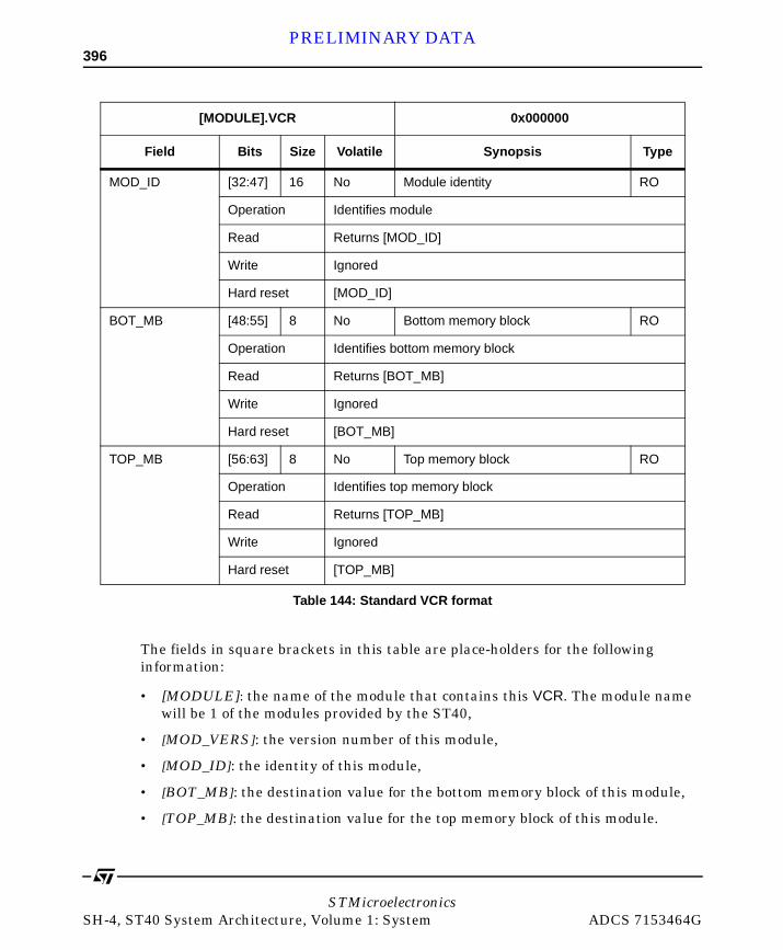
396PRELIMINARY DATA
The fields in square brackets in this table are place-holders for the following information:
• [MODULE]: the name of the module that contains this VCR. The module name will be 1 of the modules provided by the ST40,
• [MOD_VERS]: the version number of this module,
• [MOD_ID]: the identity of this module,
• [BOT_MB]: the destination value for the bottom memory block of this module,
• [TOP_MB]: the destination value for the top memory block of this module.
MOD_ID [32:47] 16 No Module identity RO
Operation Identifies module
Read Returns [MOD_ID]
Write Ignored
Hard reset [MOD_ID]
BOT_MB [48:55] 8 No Bottom memory block RO
Operation Identifies bottom memory block
Read Returns [BOT_MB]
Write Ignored
Hard reset [BOT_MB]
TOP_MB [56:63] 8 No Top memory block RO
Operation Identifies top memory block
Read Returns [TOP_MB]
Write Ignored
Hard reset [TOP_MB]
[MODULE].VCR 0x000000
Field Bits Size Volatile Synopsis Type
Table 144: Standard VCR format
STMicroelectronicsSH-4, ST40 System Architecture, Volume 1: System ADCS 7153464G

397PRELIMINARY DATA
A.1.4 P-ERROR flags
The P-ERROR flags are a set of 8 flags in a ST40 module’s VCR which indicate errors in the interface between that module and the packet-router. 2 of these error flags are reserved and always read 0. The remaining 6 error flags are used in a standard way by all ST40 modules, though not all modules implement all of these flags. If a module does not implement a particular P-ERROR flag, then that flag has reserved behavior.
All P-ERROR flags are 0 after hard reset. Implemented P-ERROR flags are volatile and are set to 1 by hardware whenever the associated error condition arises. The P-ERROR flags will be cleared autonomously by hardware only at hard reset. Software can read and write these flags at any time using appropriate accesses.
It is possible for multiple error conditions to be triggered by a single request. The actual behavior in such cases is specified by the module receiving that request.
The complete set of supported P-ERROR flags is given in Table 145.
Bit Name Bit Size Volatile Synopsis Type
ERR_RCV 0 1 Yes An error response has been received RW or Res
Operation Indicates that an earlier request from that module was invalid
This bit is set by the module hardware if an error response is received by that module from the packet-router. It is cleared autonomously by hardware only at hard reset.
Read Returns current value
Write Updates the current value if this bit is implemented by this module
Ignored if this bit is not implemented by this module
Software may write to this bit at any time.
Hard reset 0
Table 145: P-ERROR flags
STMicroelectronicsADCS 7153464G SH-4, ST40 System Architecture, Volume 1: System
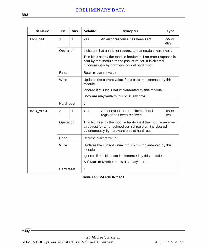
398PRELIMINARY DATA
ERR_SNT 1 1 Yes An error response has been sent RW or RES
Operation Indicates that an earlier request to that module was invalid
This bit is set by the module hardware if an error response is sent by that module to the packet-router. It is cleared autonomously by hardware only at hard reset.
Read Returns current value
Write Updates the current value if this bit is implemented by this module
Ignored if this bit is not implemented by this module
Software may write to this bit at any time.
Hard reset 0
BAD_ADDR 2 1 Yes A request for an undefined control register has been received
RW or Res
Operation This bit is set by the module hardware if the module receives a request for an undefined control register. It is cleared autonomously by hardware only at hard reset.
Read Returns current value
Write Updates the current value if this bit is implemented by this module
Ignored if this bit is not implemented by this module
Software may write to this bit at any time.
Hard reset 0
Bit Name Bit Size Volatile Synopsis Type
Table 145: P-ERROR flags
STMicroelectronicsSH-4, ST40 System Architecture, Volume 1: System ADCS 7153464G
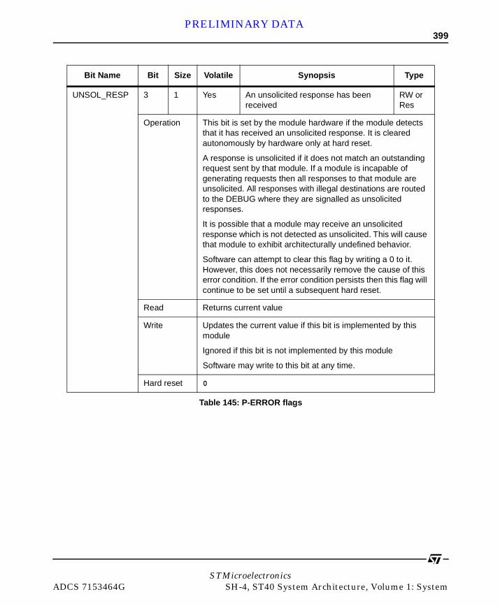
399PRELIMINARY DATA
UNSOL_RESP 3 1 Yes An unsolicited response has been received
RW or Res
Operation This bit is set by the module hardware if the module detects that it has received an unsolicited response. It is cleared autonomously by hardware only at hard reset.
A response is unsolicited if it does not match an outstanding request sent by that module. If a module is incapable of generating requests then all responses to that module are unsolicited. All responses with illegal destinations are routed to the DEBUG where they are signalled as unsolicited responses.
It is possible that a module may receive an unsolicited response which is not detected as unsolicited. This will cause that module to exhibit architecturally undefined behavior.
Software can attempt to clear this flag by writing a 0 to it. However, this does not necessarily remove the cause of this error condition. If the error condition persists then this flag will continue to be set until a subsequent hard reset.
Read Returns current value
Write Updates the current value if this bit is implemented by this module
Ignored if this bit is not implemented by this module
Software may write to this bit at any time.
Hard reset 0
Bit Name Bit Size Volatile Synopsis Type
Table 145: P-ERROR flags
STMicroelectronicsADCS 7153464G SH-4, ST40 System Architecture, Volume 1: System

400PRELIMINARY DATA
BAD_DEST 4 1 Yes A request with an illegal destination has been received
RW or Res
Operation This bit is set by the module hardware if a request with an illegal destination is received by that module from the packet-router. This bit will be cleared autonomously by hardware only at hard reset.
Read Returns current value
Write If this bit is implemented by this module, writes update the current value. If this bit is not implemented by this module, writes are ignored. Software may write to this bit at any time.
Hard reset 0
BAD_OPC 5 1 Yes A request with an unsupported opcode has been received
RW or Res
Operation This bit is set by the module hardware if a request with an unsupported opcode is received by that module from the packet-router. This error can arise because not all modules support all packet-router opcodes. This bit will be cleared autonomously by hardware only at hard reset.
Read Returns current value
Write Updates the current value if this bit is implemented by this module
Ignored if this bit is not implemented by this module
Software may write to this bit at any time.
Hard reset 0
- [6:7] 2 - Reserved Res
Operation Reserved
Read Returns 0
Write Ignored
Hard reset 0
Bit Name Bit Size Volatile Synopsis Type
Table 145: P-ERROR flags
STMicroelectronicsSH-4, ST40 System Architecture, Volume 1: System ADCS 7153464G
401PRELIMINARY DATA
A.1.5 M-ERROR flags
The M-ERROR flags are a set of 8 flags in a module’s VCR which indicate errors specific to that module. If a module does not implement a particular M-ERROR flag, then that flag has reserved behavior.
All M-ERROR flags are 0 after hard reset. Implemented M-ERROR flags are volatile and are set to 1 by hardware whenever the associated error condition arises. The M-ERROR flags will be cleared autonomously by hardware only after hard reset. Software can read and write these flags at any time using appropriate accesses.
A.1.6 Memory map conventions
The ST40 physical memory map is organized so that each control block contains a VCR at offset 0. Additionally, the address range of each data block is described by the VCR of its associated control block. In general, each control block is allocated at a higher address than its data block.
This organization allows software to scan the ST40 memory map to locate control blocks and data blocks. The software can run on a ST40 CPU, or it can run on the host and access ST40 memory using the debug link protocol. The scanning can be achieved in a safe manner with accesses that do not cause major changes to the architectural state of the system. The scanning algorithm scans downwards through the memory map reading 8-byte words from addresses aligned to 224 bytes.
This scan should start at the highest address aligned to 224 i.e. 0xFF000000. The BOT_MB and TOP_MB information in the VCR of each control block should be used to ensure that data blocks are skipped over in the scanning sequence. It is important to ensure that data blocks are not read from, since data blocks may correspond to areas of data that have to be configured carefully and to address space that is implemented using off-chip state. It is possible that reads from off-chip state could modify the state of external memory-mapped peripherals.
STMicroelectronicsADCS 7153464G SH-4, ST40 System Architecture, Volume 1: System

402PRELIMINARY DATA
Each 8-byte quadword that is read is to the first 8-byte quad word in a memory block. If the access is to an undefined block then the access will be to an illegal destination address. This will cause the following behavior:
• DEBUG.VCR.PERR_FLAGS.BAD_ADDR will be set since the access will cause a request to an illegal destination to be sent to the DEBUG module.
• DEBUG.VCR.PERR_FLAGS.ERR_SNT will be set since the access will cause an error response to be returned by the DEBUG.
• If the access is to a control block then the access will return the value of the VCR for that control block without setting any error bit nor generating an error response.
These different behaviors can be used to distinguish accesses to an undefined block from accesses to a control block. The scanning algorithm detects data blocks through the VCR values of control blocks. The scanning algorithm itself makes no accesses to locations within data blocks.
This algorithm can be used to classify each ST40 memory block between 0x00000000 and 0xFF000000 (inclusive) as a control block, a data block or an undefined block. Since each VCR value contains a module identity and module version, it is possible for software to check for the presence of particular modules and to handle different module versions appropriately.
A.1.7 P-MODULE specification standards
The specification of each module defines the functionality provided by that module. Each module defines the following:
• The memory map of each memory block associated with that module. In particular, the memory map of each control block associated with that module indicates whether each control register in that block has defined, reserved or undefined behavior.
• The interactions of that module with the SuperHyway packet-router. This includes the set of transactions that can be initiated by that module, and the transactions that can be serviced by that module. The behavior and signalling of error cases is also fully described.
• The format of all control registers defined by that module and the behavior of all fields in each control register for different types of access.
STMicroelectronicsSH-4, ST40 System Architecture, Volume 1: System ADCS 7153464G
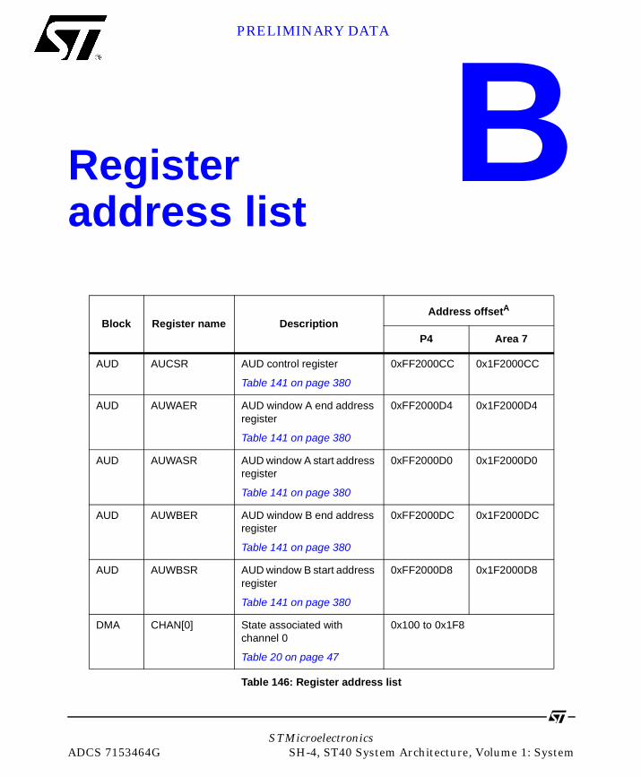
PRELIMINARY DATA
STMicroelectroniADCS 7153464G SH-4, ST40 S
B
Register address listBlock Register name DescriptionAddress offsetA
P4 Area 7
AUD AUCSR AUD control register
Table 141 on page 380
0xFF2000CC 0x1F2000CC
AUD AUWAER AUD window A end address register
Table 141 on page 380
0xFF2000D4 0x1F2000D4
AUD AUWASR AUD window A start address register
Table 141 on page 380
0xFF2000D0 0x1F2000D0
AUD AUWBER AUD window B end address register
Table 141 on page 380
0xFF2000DC 0x1F2000DC
AUD AUWBSR AUD window B start address register
Table 141 on page 380
0xFF2000D8 0x1F2000D8
DMA CHAN[0] State associated with channel 0
Table 20 on page 47
0x100 to 0x1F8
Table 146: Register address list
csystem Architecture, Volume 1: System

404PRELIMINARY DATA
DMA CHAN[0].ACTION
Cause action on a control bit associated with this channel
Table 35 on page 83
0x20
DMA CHAN[0].CONTROL
Channel control
Table 45 on page 93
0x80
DMA CHAN[0].COUNT
Channel count
Table 46 on page 99
0x88
DMA CHAN[0].DAR
Channel destination address
Table 48 on page 101
0x98
DMA CHAN[0].DISABLE
Disable a control bit associated with this channel
Table 33 on page 77
0x10
DMA CHAN[0].ENABLE
Enable a control bit associated with this channel
Table 32 on page 75
0x08
DMA CHAN[0].IDENTITY
Channel identity
Table 31 on page 71
0x00
DMA CHAN[0].POINTER
Pointer to the current or last register memory image
Table 36 on page 85
0x28
DMA CHAN[0].SAR
Channel source address
Table 47 on page 100
0x90
DMA CHAN[0].STATUS
Status of a control bit associated with this channel
Table 34 on page 80
0x18
Block Register name DescriptionAddress offsetA
P4 Area 7
Table 146: Register address list
STMicroelectronicsSH-4, ST40 System Architecture, Volume 1: System ADCS 7153464G

405PRELIMINARY DATA
DMA CHAN[0].SUBBASE
Base pointer to the table of register images in main memory
Table 38 on page 88
0x30
DMA CHAN[0].SUBDISABLE
Subheading disable
Table 40 on page 90
0x40
DMA CHAN[0].SUBENABLE
Subchannel enable
Table 39 on page 89
0x38
DMA CHAN[0].SUBINT_ACT
Subchannel interrupt action
Table 44 on page 92
0x60
DMA CHAN[0].SUBINT_DIS
Subchannel interrupt disable
Table 42 on page 91
0x50
DMA CHAN[0].SUBINT_ENB
Subchannel interrupt enable
Table 41 on page 90
0x48
DMA CHAN[0].SUBINT_STAT
Subchannel interrupt status
Table 44 on page 92
0x58
DMA CHAN[1:4].CONTROL
Channel control
Table 45 on page 93
0x80
DMA CHAN[1:4].COUNT
Channel count
Table 46 on page 99
0x88
DMA CHAN[1:4].DAR
Channel destination address
Table 48 on page 101
0x98
DMA CHAN[1:4].DISABLE
Disable or reset a control bit associated with this channel
Table 33 on page 77
0x10
Block Register name DescriptionAddress offsetA
P4 Area 7
Table 146: Register address list
STMicroelectronicsADCS 7153464G SH-4, ST40 System Architecture, Volume 1: System
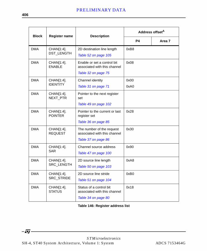
406PRELIMINARY DATA
DMA CHAN[1:4].DST_LENGTH
2D destination line length
Table 52 on page 105
0xB8
DMA CHAN[1:4].ENABLE
Enable or set a control bit associated with this channel
Table 32 on page 75
0x08
DMA CHAN[1:4].IDENTITY
Channel identity
Table 31 on page 71
0x00
0xA0
DMA CHAN[1:4].NEXT_PTR
Pointer to the next register set
Table 49 on page 102
DMA CHAN[1:4].POINTER
Pointer to the current or last register set
Table 36 on page 85
0x28
DMA CHAN[1:4].REQUEST
The number of the request associated with this channel
Table 37 on page 86
0x30
DMA CHAN[1:4].SAR
Channel source address
Table 47 on page 100
0x90
DMA CHAN[1:4].SRC_LENGTH
2D source line length
Table 50 on page 103
0xA8
DMA CHAN[1:4].SRC_STRIDE
2D source line stride
Table 51 on page 104
0xB0
DMA CHAN[1:4].STATUS
Status of a control bit associated with this channel
Table 34 on page 80
0x18
Block Register name DescriptionAddress offsetA
P4 Area 7
Table 146: Register address list
STMicroelectronicsSH-4, ST40 System Architecture, Volume 1: System ADCS 7153464G

407PRELIMINARY DATA
DMA CHAN[1] State associated with channel 1
Table 21 on page 49
0x200 to 0x2F8
DMA CHAN[2] State associated with channel 2
Table 21 on page 49
0x300 to 0x3F8
DMA CHAN[3] State associated with channel 3
Table 21 on page 49
0x400 to 0x4F8
DMA CHAN[4] State associated with channel 4
Table 21 on page 49
0x500 to 0x4F8
DMA CHANNEL[1:4].ACTION
Cause action on a control bit associated with this channel
Table 35 on page 83
0x20
DMA DEFINED Global DMA channel defined
Table 29 on page 70
0x38
DMA DISABLE Global disable
Table 25 on page 66
0x18
DMA ENABLE Global enable
Table 24 on page 65
0x10
DMA ERROR Global error status
Table 28 on page 69
0x30
DMA HANDSHAKE Global request handshake protocol
Table 30 on page 70
0x40
Block Register name DescriptionAddress offsetA
P4 Area 7
Table 146: Register address list
STMicroelectronicsADCS 7153464G SH-4, ST40 System Architecture, Volume 1: System
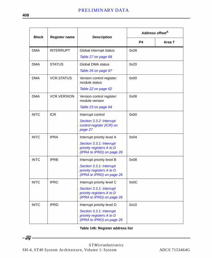
408PRELIMINARY DATA
DMA INTERRUPT Global interrupt status
Table 27 on page 68
0x28
DMA STATUS Global DMA status
Table 26 on page 67
0x20
DMA VCR.STATUS Version control register: module status
Table 22 on page 62
0x00
DMA VCR.VERSION Version control register: module version
Table 23 on page 64
0x08
INTC ICR Interrupt control
Section 3.3.2: Interrupt control register (ICR) on page 27
0x00
INTC IPRA Interrupt priority level A
Section 3.3.1: Interrupt priority registers A to D (IPRA to IPRD) on page 26
0x04
INTC IPRB Interrupt priority level B
Section 3.3.1: Interrupt priority registers A to D (IPRA to IPRD) on page 26
0x08
INTC IPRC Interrupt priority level C
Section 3.3.1: Interrupt priority registers A to D (IPRA to IPRD) on page 26
0x0C
INTC IPRD Interrupt priority level D
Section 3.3.1: Interrupt priority registers A to D (IPRA to IPRD) on page 26
0x10
Block Register name DescriptionAddress offsetA
P4 Area 7
Table 146: Register address list
STMicroelectronicsSH-4, ST40 System Architecture, Volume 1: System ADCS 7153464G
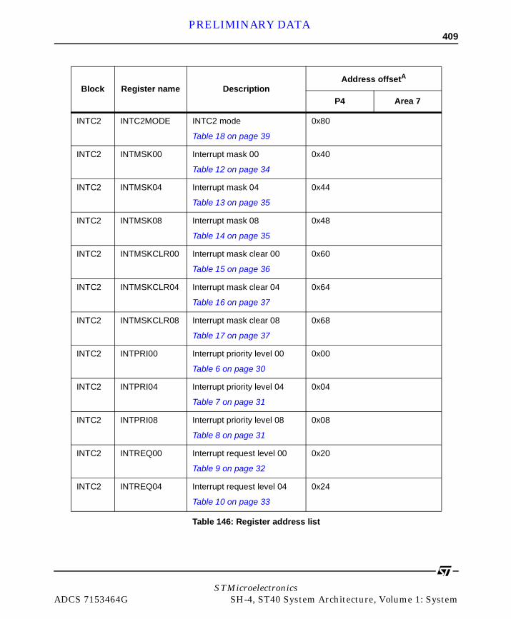
409PRELIMINARY DATA
INTC2 INTC2MODE INTC2 mode
Table 18 on page 39
0x80
INTC2 INTMSK00 Interrupt mask 00
Table 12 on page 34
0x40
INTC2 INTMSK04 Interrupt mask 04
Table 13 on page 35
0x44
INTC2 INTMSK08 Interrupt mask 08
Table 14 on page 35
0x48
INTC2 INTMSKCLR00 Interrupt mask clear 00
Table 15 on page 36
0x60
INTC2 INTMSKCLR04 Interrupt mask clear 04
Table 16 on page 37
0x64
INTC2 INTMSKCLR08 Interrupt mask clear 08
Table 17 on page 37
0x68
INTC2 INTPRI00 Interrupt priority level 00
Table 6 on page 30
0x00
INTC2 INTPRI04 Interrupt priority level 04
Table 7 on page 31
0x04
INTC2 INTPRI08 Interrupt priority level 08
Table 8 on page 31
0x08
INTC2 INTREQ00 Interrupt request level 00
Table 9 on page 32
0x20
INTC2 INTREQ04 Interrupt request level 04
Table 10 on page 33
0x24
Block Register name DescriptionAddress offsetA
P4 Area 7
Table 146: Register address list
STMicroelectronicsADCS 7153464G SH-4, ST40 System Architecture, Volume 1: System
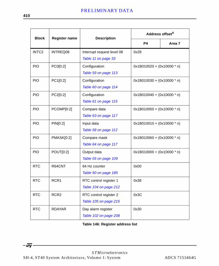
410PRELIMINARY DATA
INTC2 INTREQ08 Interrupt request level 08
Table 11 on page 33
0x28
PIO PC0[0:2] Configuration
Table 59 on page 113
0x1B010020 + (0x10000 * n)
PIO PC1[0:2] Configuration
Table 60 on page 114
0x1B010030 + (0x10000 * n)
PIO PC2[0:2] Configuration
Table 61 on page 115
0x1B010040 + (0x10000 * n)
PIO PCOMP[0:2] Compare data
Table 63 on page 117
0x1B010050 + (0x10000 * n)
PIO PIN[0:2] Input data
Table 58 on page 112
0x1B010010 + (0x10000 * n)
PIO PMASK[0:2] Compare mask
Table 64 on page 117
0x1B010060 + (0x10000 * n)
PIO POUT[0:2] Output data
Table 55 on page 109
0x1B010000 + (0x10000 * n)
RTC R64CNT 64 Hz counter
Table 90 on page 185
0x00
RTC RCR1 RTC control register 1
Table 104 on page 212
0x38
RTC RCR2 RTC control register 2
Table 105 on page 215
0x3C
RTC RDAYAR Day alarm register
Table 102 on page 208
0x30
Block Register name DescriptionAddress offsetA
P4 Area 7
Table 146: Register address list
STMicroelectronicsSH-4, ST40 System Architecture, Volume 1: System ADCS 7153464G

411PRELIMINARY DATA
RTC RDAYCNT Day counter
Table 95 on page 194
0x14
RTC RHRAR Hour alarm register
Table 100 on page 204
0x28
RTC RHRCNT Hour counter
Table 93 on page 190
0x0C
RTC RMINAR Minute alarm register
Table 99 on page 202
0x24
RTC RMINCNT Minute counter
Table 92 on page 188
0x08
RTC RMONAR Month alarm register
Table 103 on page 210
0x34
RTC RMONCNT Month counter
Table 96 on page 196
0x18
RTC RSECAR Second alarm register
Table 98 on page 200
0x20
RTC RSECCNT Second counter
Table 91 on page 186
0x04
RTC RWKAR Day of week alarm register
Table 101 on page 206
0x2C
RTC RWKCNT Day of week counter
Table 94 on page 192
0x10
RTC RYRCNT Year counter
Table 97 on page 198
0x1C
Block Register name DescriptionAddress offsetA
P4 Area 7
Table 146: Register address list
STMicroelectronicsADCS 7153464G SH-4, ST40 System Architecture, Volume 1: System
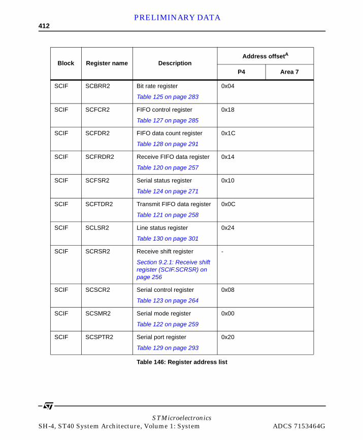
412PRELIMINARY DATA
SCIF SCBRR2 Bit rate register
Table 125 on page 283
0x04
SCIF SCFCR2 FIFO control register
Table 127 on page 285
0x18
SCIF SCFDR2 FIFO data count register
Table 128 on page 291
0x1C
SCIF SCFRDR2 Receive FIFO data register
Table 120 on page 257
0x14
SCIF SCFSR2 Serial status register
Table 124 on page 271
0x10
SCIF SCFTDR2 Transmit FIFO data register
Table 121 on page 258
0x0C
SCIF SCLSR2 Line status register
Table 130 on page 301
0x24
SCIF SCRSR2 Receive shift register
Section 9.2.1: Receive shift register (SCIF.SCRSR) on page 256
-
SCIF SCSCR2 Serial control register
Table 123 on page 264
0x08
SCIF SCSMR2 Serial mode register
Table 122 on page 259
0x00
SCIF SCSPTR2 Serial port register
Table 129 on page 293
0x20
Block Register name DescriptionAddress offsetA
P4 Area 7
Table 146: Register address list
STMicroelectronicsSH-4, ST40 System Architecture, Volume 1: System ADCS 7153464G
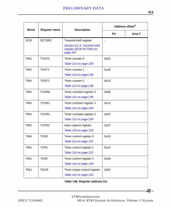
413PRELIMINARY DATA
SCIF SCTSR2 Transmit shift register
Section 9.2.3: Transmit shift register (SCIF.SCTSR) on page 257
-
TMU TCNT0 Timer counter 0
Table 113 on page 236
0x0C
TMU TCNT1 Timer counter 1
Table 113 on page 236
0x18
TMU TCNT2 Timer counter 2
Table 113 on page 236
0x24
TMU TCOR0 Timer constant register 0
Table 112 on page 235
0x08
TMU TCOR1 Timer constant register 1
Table 112 on page 235
0x14
TMU TCOR2 Timer constant register 2
Table 112 on page 235
0x20
TMU TCPR2 Input capture register
Table 116 on page 243
0x2C
TMU TCR0 Timer control register 0
Table 114 on page 237
0x10
TMU TCR1 Timer control register 1
Table 114 on page 237
0x1C
TMU TCR2 Timer control register 2
Table 115 on page 239
0x28
TMU TOCR Timer output control register
Table 110 on page 232
0x00
Block Register name DescriptionAddress offsetA
P4 Area 7
Table 146: Register address list
STMicroelectronicsADCS 7153464G SH-4, ST40 System Architecture, Volume 1: System

414PRELIMINARY DATA
TMU TSTR Timer start register
Table 111 on page 233
0x04
UBC BAMRA Break address mask register A
Section 10.3.4: Break address mask register A (UBC.BAMRA) on page 329
0xFF200004 0x1F200004
UBC BAMRB Break address mask register B
Section 10.3.8: Break address mask register B (UBC.BAMRB) on page 333
0xFF200010 0x1F200010
UBC BARA Break address register A
Section 10.3.2: Break address register A (UBC.BARA) on page 328
0xFF200000 0x1F200000
UBC BARB Break address register B
Section 10.3.6: Break address register B (UBC.BARB) on page 333
0xFF20000C 1F20000C
UBC BASRA Break ASID register A
Section 10.3.3: Break ASID register A (UBC.BASRA) on page 329
0xFF000014 0x1F000014
UBC BASRB Break ASID register B
Section 10.3.7: Break ASID register B (UBC.BASRB) on page 333
0xFF000018 0x1F000018
Block Register name DescriptionAddress offsetA
P4 Area 7
Table 146: Register address list
STMicroelectronicsSH-4, ST40 System Architecture, Volume 1: System ADCS 7153464G
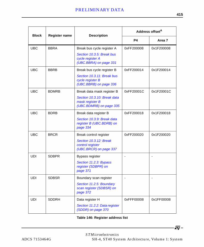
415PRELIMINARY DATA
UBC BBRA Break bus cycle register A
Section 10.3.5: Break bus cycle register A (UBC.BBRA) on page 331
0xFF200008 0x1F200008
UBC BBRB Break bus cycle register B
Section 10.3.11: Break bus cycle register B (UBC.BBRB) on page 336
0xFF200014 0x1F200014
UBC BDMRB Break data mask register B
Section 10.3.10: Break data mask register B (UBC.BDMRB) on page 335
0xFF20001C 0x1F20001C
UBC BDRB Break data register B
Section 10.3.9: Break data register B (UBC.BDRB) on page 334
0xFF200018 0x1F200018
UBC BRCR Break control register
Section 10.3.12: Break control register (UBC.BRCR) on page 337
0xFF200020 0x1F200020
UDI SDBPR Bypass register
Section 11.2.3: Bypass register (SDBPR) on page 371
- -
UDI SDBSR Boundary scan register
Section 11.2.5: Boundary scan register (SDBSR) on page 372
- -
UDI SDDRH Data register H
Section 11.2.2: Data register (SDDR) on page 370
0xFFF00008 0x1FF00008
Block Register name DescriptionAddress offsetA
P4 Area 7
Table 146: Register address list
STMicroelectronicsADCS 7153464G SH-4, ST40 System Architecture, Volume 1: System
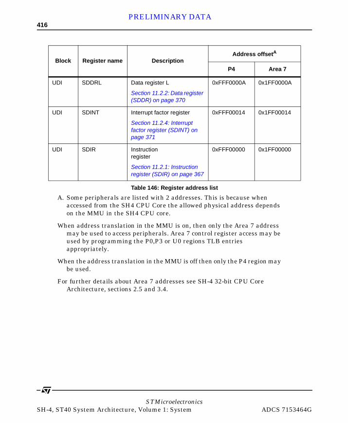
416PRELIMINARY DATA
UDI SDDRL Data register L
Section 11.2.2: Data register (SDDR) on page 370
0xFFF0000A 0x1FF0000A
UDI SDINT Interrupt factor register
Section 11.2.4: Interrupt factor register (SDINT) on page 371
0xFFF00014 0x1FF00014
UDI SDIR Instruction register
Section 11.2.1: Instruction register (SDIR) on page 367
0xFFF00000 0x1FF00000
A. Some peripherals are listed with 2 addresses. This is because when accessed from the SH4 CPU Core the allowed physical address depends on the MMU in the SH4 CPU core.
When address translation in the MMU is on, then only the Area 7 address may be used to access peripherals. Area 7 control register access may be used by programming the P0,P3 or U0 regions TLB entries appropriately.
When the address translation in the MMU is off then only the P4 region may be used.
For further details about Area 7 addresses see SH-4 32-bit CPU Core Architecture, sections 2.5 and 3.4.
Block Register name DescriptionAddress offsetA
P4 Area 7
Table 146: Register address list
STMicroelectronicsSH-4, ST40 System Architecture, Volume 1: System ADCS 7153464G

417PRELIMINARY DATA
Index
AAddress 4-5, 9, 11, 13, 23, 40, 43, 45-46,
48-50, 52, 55-56, 61, 73, 81, 85, 88, 100-106, 108, 118-119, 122-123, 154, 182, 230, 255-256, 321-322, 324-325, 328-330, 333, 341-345, 347-348, 350, 352-357, 364, 374, 377, 379-382, 384-385, 390-391, 394-395, 401-406, 414
Address map 13, 45, 122-123, 182, 230, 256
Af 212Aie 213Alarm 180, 183, 200-213, 222-223,
410-411Alarm interrupts 180, 223Aligned 43, 53, 81, 108, 118, 390, 401Alignment 52-53, 63, 74, 76, 78, 81, 84,
99-101, 103-106AND 249Architectural state 401ASE 1, 5, 380-385
BBackus-Naur Form xxiiiBad_addr 398Bad_dest 400Bad_opc 400BNF. See Backus-naur Form.
Bootstrap 58BOT_MB 396Bot_mb 394-396, 401Branch instruction 341, 344, 347Break 5, 40, 173, 252, 254, 265, 267,
269, 272, 279, 293, 298, 303, 313, 315-317, 321-326, 328-340, 342-356, 381-385, 414-415
BRK 267-270, 272, 279, 313, 315-316Byte 154, 333, 345
CCACHE 4Cache 4-5, 172Carry interrupt 180, 213, 222-223Cf 214Channel 5-6, 43-55, 57-61, 63, 65-81,
83-86, 88-94, 98-106, 109, 167-168, 227-228, 233-237, 239, 242-244, 248-250, 321, 328-340, 342-345, 348-349, 351, 353-357, 381-382, 403-407
Character 251, 260, 262-263, 273, 277, 303
CHR 260-261, 304-305Cie 213CKE 264, 269-270, 303-304, 306CKEG 237, 239-240, 243-244, 247-248CKS 155, 157, 159-160, 173, 259, 263,
STMicroelectronicsADCS 7153464G SH-4, ST40 System Architecture, Volume 1: System

418PRELIMINARY DATA
282, 284Clock output pin 232Clock pause function 174Compatibility 1Configuration register (CFG) 107,
113-115Control block 389-391, 393-395, 401-402Control registers (CR) 17, 20, 27, 122,
159, 164-165, 168-169, 173, 175, 183, 185, 230, 235, 244, 248, 255, 268-269, 271-272, 278, 281, 303, 309, 316-317, 326-327, 337, 342-345, 361, 364, 374, 380, 384-385, 390-394, 398, 402-403, 408, 410, 412-413, 415
COUNT 48-49, 55-57, 404-405CPG 122, 134, 154-162, 164-165,
168-169, 171-173, 175-176, 364Crystal oscillator 6, 179, 216, 224CTSDT 294, 296-297
DDAR 48, 50, 97, 404-405Data 3, 5, 9, 36-37, 39, 43-44, 51-57,
60-61, 72-73, 93, 95-97, 99-101, 103-105, 107-112, 116-117, 119, 136-137, 142-143, 158, 220, 228, 239, 241, 251-252, 254-258, 261, 267-268, 270-274, 276-282, 284-286, 288-298, 303-306, 308-311, 313-318, 325-326, 334-336, 339, 341-345, 347, 350, 354-357, 361, 363-364, 366, 370, 377, 379, 381-382, 384-385, 389, 401, 410, 412, 415-416
Data block 389-390, 394-395, 401-402Day 179-180, 183, 192, 194, 196,
206-209, 215, 222, 410-411DBR 352, 382DEBUG 5, 399, 402Debug 1, 5, 62, 337, 340, 352, 361, 390,
401DEBUG.VCR 402Delayed branch 3, 342, 344, 347Denormalize 3DMA 43-47, 49-62, 64-72, 75, 77, 80,
83-86, 88-94, 99-106, 162, 168, 173, 252, 315, 390, 403, 407-408
DMA.STATUS 45, 66-67, 408DMAC 5, 44-45, 53-54, 161, 228, 239,
241, 248, 252, 269, 277-278, 281-282, 315-316, 319
Double 8Dreq 70
EENB 184, 200, 202, 204, 206, 208, 210,
212, 222Enb 201, 203, 205, 207, 209, 211Endian 44
Big-endian 44, 57Endianess 57Little-endian 61
ER 267-270, 273-274, 276, 313, 316Err_rcv 390, 397Err_snt 398Errors 78, 81, 84, 252, 270, 273-274,
303, 390, 397, 401Event 22-23, 40, 60, 72, 94, 176-177,
222, 236, 239, 241, 252, 290, 351-352, 356, 377
Exception 3, 15, 20, 22-23, 38-39, 171, 174-175, 316, 342-344, 346-348, 350-352, 374-375
EXTAL 174, 182
FFDIV 3FER 268, 270, 272-274, 280, 317
STMicroelectronicsSH-4, ST40 System Architecture, Volume 1: System ADCS 7153464G
419PRELIMINARY DATA
FIFO 6, 25, 251-252, 255-258, 267-272, 278, 281, 284-286, 288-291, 302-303, 309, 316-317, 377, 412
FIPR 4Floating-point 3, 327FMAC 3FPU 1, 3Frame 252, 279, 282, 305, 309-310FSQRT 3FTRV 4Function 5-6, 15, 52, 107, 113, 116, 162,
165, 174-177, 179-180, 182, 220, 227, 229, 237, 239-241, 243-244, 248-249, 254, 304, 317, 321, 337, 340, 352, 363, 374, 377, 381
Functions 1, 6, 162, 179, 252, 254, 270, 321, 361, 375, 380-381
GGraphics 4
HHour 179-180, 183, 190, 192, 194,
204-205, 215, 220, 222, 411
IICPE 241, 243-244, 249Identifier 4IEEE754 3IF 56Instruction set 1, 344INTC 15-17, 19, 25-26, 38-40, 160, 409Interrupt controller 40, 173, 269, 315,
319IOVF 155, 157, 160IRL 5, 17, 19-24, 26, 29, 38, 171-172,
174-175IRLM 22, 29
JJTAG 5, 361, 363, 372, 374
LLeap year 180, 194, 208Link 82, 94, 401LIST 94Load 3Load instruction 327Loading 58LoadWord 390LOCK 138, 144Long 159
MMap 38, 401Matrix 4MCE 254, 285, 289, 296MDIV 136, 139, 142, 145Memory 4-5, 7, 42-44, 46-47, 49, 52-54,
57-61, 67, 80-81, 88-89, 93, 102, 162, 173, 327, 341, 343, 347, 377, 389-390, 401, 404-405
Memory block 389, 396, 402Memory map 401-402Merr_flags 394-395Minute 179-180, 183, 188, 190, 202,
215-216, 222, 411Misaligned 78MMU 1, 4MOD_ID 396Mod_id 63, 394, 396MOD_VERS 396Mod_vers 394-395Mode 1, 3-6, 19-21, 26-29, 38, 40, 53, 76,
79, 107, 154-157, 159-162, 164-166, 171-176, 182, 184-186, 188, 190, 192,
STMicroelectronicsADCS 7153464G SH-4, ST40 System Architecture, Volume 1: System

420PRELIMINARY DATA
194, 196, 198, 200, 202, 204, 206, 208, 210, 212, 215, 227, 231-236, 243-244, 248, 254, 259-261, 264, 268, 270, 276, 283-284, 293, 296-297, 303-304, 309, 318-319, 331, 337, 343, 353-357, 361, 363, 367, 371, 374-375, 377, 380, 382, 409
Privileged 382Switch 154
MODULE 395-396Month 179-180, 183, 194, 196, 198, 208,
210-211, 215, 222, 411MOV.W 341MSTP 163, 165, 167-170, 175-176
NName 17, 45, 47, 49, 154, 164-165, 182,
229, 254-255, 364, 366, 379, 384, 390, 393, 396-397, 403
NDIV 136, 142NMI 5, 15, 17, 19-20, 23, 27-28, 159,
171-172, 174-175Notation 393
OO/E 260-262, 276Object 1OCBI 341, 345OCBP 341, 345OCBWB 341, 345On-chip peripheral 5, 22-23, 26, 162,
167-168, 171-172, 174-175, 364Opcode 400Operand 4, 321, 331-333, 336, 341-343,
345-350, 354, 356-357, 381OR 350OTHER 136-138, 140-141, 143Outputs 296, 298, 377
PPacket-router 7-11, 13, 394, 397-398,
400, 402Parity 251-252, 260-262, 271, 273-274,
276, 280, 303-304, 309-310, 313-314, 317
PC 40, 107, 113-116, 338-339, 347PCI 161, 176-177PDIV 137, 143PE 260-261, 304-305Pef 218PER 268, 270-271, 274, 280, 317Performance counters 1Periodic 215, 217-218, 223Periodic interrupts 180, 217, 223Perr_flags 390, 394Pes 217Physical memory 401PHZ 165-166Pipe-lining 10Pipelining 54PLL 6, 127, 134, 136-139, 142-144, 159PLL1EN 134PMU 161POWER 6Power management 121, 161Power-on reset 19, 27, 154-156, 169, 176,
200, 202, 204, 206, 208, 210, 215, 254, 257-259, 264, 270, 276-284, 290, 293, 296-298, 302, 328-329, 331, 334, 336-340, 373
P-port 8, 395P-protocol 10PPU 165-166Precision
Double 3Single 3-4
STMicroelectronicsSH-4, ST40 System Architecture, Volume 1: System ADCS 7153464G
421PRELIMINARY DATA
PREF 341, 345Priority 5, 15, 17-23, 26, 30-31, 40, 42,
54-55, 57, 250, 315-316, 374, 408-409
Priority Register 26, 30Process 11
RRDF 267-268, 270-271, 281, 286, 288,
313, 315-317RE 254, 265, 268-269, 274, 302, 306REAL-TIME 6Register 15, 17-20, 22-23, 26-27, 30-40,
44-47, 49-50, 52-54, 57-71, 74-75, 77, 80, 83-86, 88-90, 93-94, 99-101, 103-119, 122-123, 134, 136-139, 142, 145, 154-155, 158-165, 167, 169-176, 179, 182, 184-186, 188, 190, 192, 194, 196, 198, 200, 202, 204, 206, 208, 210, 212, 214-215, 222-223, 228, 230, 232-237, 239-240, 243-244, 248, 250-252, 254-259, 263-264, 267, 269-270, 278, 281-284, 291, 293, 301, 303, 313, 316-317, 324-329, 331, 333-337, 339, 342-345, 347-348, 352-356, 361, 364-367, 370-371, 377, 380, 384-385, 389-391, 393, 404-406, 408-410, 412-416
DR 252, 267-268, 270-271, 282, 313, 315-316
EXPEVT 347-348Field Type
READ-ONLY 63-64, 67-74, 80-81, 85-87, 91, 108, 112, 117, 138, 144, 185, 187, 189, 191, 193, 195, 197, 201, 203, 205, 207, 209, 211-213, 232, 234, 238, 242-243, 257, 259-260, 264, 266, 271-274, 286-287, 291-292, 294-295, 302, 395-396
READ-WRITE 30-31, 34-35, 62-63,
65, 70, 75-76, 86-90, 93-97, 99-106, 109, 113-115, 182-183, 186, 188, 190, 192, 194, 196, 198-200, 202, 204, 206, 208, 210, 212-218, 238, 240-241, 397-400
RESERVED 135, 138, 141, 146-152, 397-400
FPSCR FieldENABLE 47, 49, 137, 143, 404, 406FLAG 39
INTEVT 22-23, 38-40, 42, 171, 174, 347-348, 374
R 17-19, 39, 108, 122, 134-135, 154-155, 164-165, 169, 230, 232-237, 239-242, 255, 259-260, 264-266, 271-273, 283, 285-286, 291, 293-295, 301, 324-326, 328-329, 331, 334-335, 337, 352, 364, 366, 370, 380
SR 17, 20, 22-23, 40, 42, 171, 174, 343SR.BL 15, 28SSR 40, 42, 171, 174, 351VBR 40, 374
RegistersFloating point 327Program Counter 40, 341, 347
REIE 265, 268-269, 313, 315RESERVED 39, 135, 138, 141, 146-152,
212-213, 259-260, 264, 266, 286, 294-295, 302, 400
Reserved bits 26RESET 154-155, 159, 165, 169, 171,
174, 176, 185, 215, 364Reset 19, 23, 26-27, 30-37, 39, 44, 49, 52,
57, 60, 62-106, 108-115, 117-118, 134-152, 154-156, 159-160, 162-163, 165, 171-172, 174, 184-218, 223, 231-243, 250, 254, 257-260, 264-266, 268-274, 276-287, 290-298, 301-302, 306, 316, 319, 328-329, 331, 334, 336-340, 343, 361, 363-364, 367,
STMicroelectronicsADCS 7153464G SH-4, ST40 System Architecture, Volume 1: System

422PRELIMINARY DATA
369-370, 373-375, 392-401, 405Response 10-11, 54, 62, 116, 381, 391,
397-399, 402RIE 265, 267-269, 313, 315RISC 1, 3Rising edge 28, 227, 237, 239-240, 248,
318, 372RSTS 155-156, 160RTC 21-22, 24-26, 163, 167, 173-176,
179, 181-186, 188, 190, 192, 194, 196, 198, 200, 202, 204, 206, 208, 210, 212, 215-216, 219-220, 222-224, 227, 229, 231-233, 236-237, 239, 247-248, 250, 410-411
RTCCLK 233, 236Rtcen 216RTE 22, 40, 42, 327, 344, 350-351, 374RTS 168, 252, 254, 289-290, 293,
295-296, 299, 303, 314RTSDT 295-296RTSIO 295-296
SSAR 48-49, 96, 404, 406SCIF 6, 22, 24-26, 167-168, 170, 175,
251-259, 261, 263-265, 267-274, 276-285, 288-289, 291-293, 296, 298-299, 301-309, 311-319, 412
Second 6, 45, 52, 54, 179-180, 182-183, 186, 188, 200-201, 214-216, 220, 222, 263, 276, 411
Section 7, 11, 107-108, 163, 166, 172, 174, 176, 256, 259-260, 263-266, 271-274, 285-286, 293-295, 301, 326, 341, 343, 391, 394-395
Segment 53Serial status register 255, 412SETUP 137, 143
SLEEP 159, 162-163, 166, 171-174, 350Sleep 6, 19-20, 28, 162, 165-166,
171-172, 175, 375SPC 40, 42, 171, 174, 347, 351SRC 50, 53, 93, 95-96, 406Stack 171, 174Standard 251, 361, 391, 393-395, 397,
402Standby 6, 19-21, 26-28, 122, 155, 159,
162-166, 168-176, 182, 184-186, 188, 190, 192, 194, 196, 198, 200, 202, 204, 206, 208, 210, 212, 215, 227, 231-236, 243, 248, 259, 264, 270, 283-284, 293, 331, 337, 375
Status bit 83-84Status register (SR) 19-20, 22-23, 40,
255, 267, 288-289, 309, 315-317, 412Status register field
ASID 4, 321-322, 324, 329-330, 333, 342, 345, 353-357, 381, 384, 414
BL 19-20, 22-23, 40, 42, 171, 174, 343, 350-351
M 318-319, 395, 401MD 40, 134, 168, 254, 299-301S 381-382, 384
STBY 162-163, 165-166, 171-173STOP 259, 262-263, 304-305Store 5, 57, 108, 118, 256, 258, 370StoreWord 390STR 233-234, 244, 250SUB 94SuperH SH-Series
documentation suitenotation xxiii
Superscalar 3Symbol 393Synchronization 228, 235, 250-251, 303,
313, 363
STMicroelectronicsSH-4, ST40 System Architecture, Volume 1: System ADCS 7153464G

423PRELIMINARY DATA
TTCLK 168, 182, 227, 229, 232-233, 236,
239, 244, 247-248TCNT 228, 233-241, 244, 246, 248, 250TCOE 232, 239, 244, 248TCOR 234-235, 244TCR 235-236, 244, 246-249TDFE 267, 270, 272, 278, 286, 289, 309,
315-316TEND 270, 273, 277, 306, 309TIE 266-267, 309, 315TLB 344TME 155, 159-160, 173TMU 22, 24-26, 167-168, 173, 175-176,
182, 227, 229-237, 239, 243-244, 248-250, 413-414
TMUBASE 230TOP_MB 396Top_mb 394-396, 401TPSC 235, 237, 239, 244, 246-248Tracing 377TRAPA 351Type 5, 19, 30-37, 39, 46, 61-71, 75, 77,
80, 83, 85-86, 88-93, 99-106, 108-115, 117, 134, 136, 139, 142, 145, 147-152, 160, 162, 185-186, 188, 190, 192, 194, 196, 198, 200, 202, 204, 206, 208, 210, 212, 215, 227, 232-233, 235-237, 239, 243, 257-259, 264, 271, 283, 285, 291, 293, 301, 344, 351, 374, 389, 392-393, 395, 397, 402
UUDI 22, 24, 26Undefined block 389-390, 402UNF 235, 238, 240-241, 244, 249UNIE 238, 240, 244, 249Unsol_resp 399
VVCR 389-391, 394-397, 401-402Volatile 30-37, 39, 62, 64-71, 75, 77, 80,
83, 85-86, 88-93, 99-106, 109-115, 117, 134, 136, 139, 142, 145, 147-152, 185-186, 188, 190, 192, 194, 196, 198, 200, 202, 204, 206, 208, 210, 212, 215, 232-233, 235-237, 239, 243, 257-259, 264, 271, 283, 285, 291, 293, 301, 392-393, 395, 397, 401
WWatchdog timer 22, 122, 154-158, 160,
165, 169, 171, 176WDT 22, 25-26, 153-157, 159-160,
173-175WinCE 1WOVF 155-156, 159-160WT/IT 155-156, 160WTCNT 122, 155, 158
XYZXTAL 182Year 179, 183, 194, 198-199, 208, 215,
220, 411
STMicroelectronicsADCS 7153464G SH-4, ST40 System Architecture, Volume 1: System

424PRELIMINARY DATA
STMicroelectronicsSH-4, ST40 System Architecture, Volume 1: System ADCS 7153464G

UM0339 Revision history
425/426
Revision history
Table 1. Document revision history
Date Revision Changes
24-May-2002 1 Initial release
12-Jul-2006 2Second revision based on ADCS 7153464_G 9 May 2003Changed cover page and disclaimer
UM0339
426/426
Please Read Carefully:
Information in this document is provided solely in connection with ST products. STMicroelectronics NV and its subsidiaries (“ST”) reserve theright to make changes, corrections, modifications or improvements, to this document, and the products and services described herein at anytime, without notice.
All ST products are sold pursuant to ST’s terms and conditions of sale.
Purchasers are solely responsible for the choice, selection and use of the ST products and services described herein, and ST assumes noliability whatsoever relating to the choice, selection or use of the ST products and services described herein.
No license, express or implied, by estoppel or otherwise, to any intellectual property rights is granted under this document. If any part of thisdocument refers to any third party products or services it shall not be deemed a license grant by ST for the use of such third party productsor services, or any intellectual property contained therein or considered as a warranty covering the use in any manner whatsoever of suchthird party products or services or any intellectual property contained therein.
UNLESS OTHERWISE SET FORTH IN ST’S TERMS AND CONDITIONS OF SALE ST DISCLAIMS ANY EXPRESS OR IMPLIEDWARRANTY WITH RESPECT TO THE USE AND/OR SALE OF ST PRODUCTS INCLUDING WITHOUT LIMITATION IMPLIEDWARRANTIES OF MERCHANTABILITY, FITNESS FOR A PARTICULAR PURPOSE (AND THEIR EQUIVALENTS UNDER THE LAWSOF ANY JURISDICTION), OR INFRINGEMENT OF ANY PATENT, COPYRIGHT OR OTHER INTELLECTUAL PROPERTY RIGHT.
UNLESS EXPRESSLY APPROVED IN WRITING BY AN AUTHORIZED ST REPRESENTATIVE, ST PRODUCTS ARE NOTRECOMMENDED, AUTHORIZED OR WARRANTED FOR USE IN MILITARY, AIR CRAFT, SPACE, LIFE SAVING, OR LIFE SUSTAININGAPPLICATIONS, NOR IN PRODUCTS OR SYSTEMS WHERE FAILURE OR MALFUNCTION MAY RESULT IN PERSONAL INJURY,DEATH, OR SEVERE PROPERTY OR ENVIRONMENTAL DAMAGE. ST PRODUCTS WHICH ARE NOT SPECIFIED AS "AUTOMOTIVEGRADE" MAY ONLY BE USED IN AUTOMOTIVE APPLICATIONS AT USER’S OWN RISK.
Resale of ST products with provisions different from the statements and/or technical features set forth in this document shall immediately voidany warranty granted by ST for the ST product or service described herein and shall not create or extend in any manner whatsoever, anyliability of ST.
ST and the ST logo are trademarks or registered trademarks of ST in various countries.
Information in this document supersedes and replaces all information previously supplied.
The ST logo is a registered trademark of STMicroelectronics. All other names are the property of their respective owners.
© 2007 STMicroelectronics - All rights reserved
STMicroelectronics group of companies
Australia - Belgium - Brazil - Canada - China - Czech Republic - Finland - France - Germany - Hong Kong - India - Israel - Italy - Japan - Malaysia - Malta - Morocco - Singapore - Spain - Sweden - Switzerland - United Kingdom - United States of America
www.st.com


