drv8837c 1-a low-voltage h-bridge driver datasheet (rev. a)
TRANSCRIPT

VCC
nSLEEP
0 to 11 V
Con
trol
ler
DRV8837C
H-Bridge PWM Driver
PWM
Protection
1 A BDCBLDC
Copyright © 2016, Texas Instruments Incorporated
3.3 or 5.0 V
Product
Folder
Sample &Buy
Technical
Documents
Tools &
Software
Support &Community
An IMPORTANT NOTICE at the end of this data sheet addresses availability, warranty, changes, use in safety-critical applications,intellectual property matters and other important disclaimers. PRODUCTION DATA.
DRV8837CSLVSD61A –JULY 2016–REVISED JULY 2016
DRV8837C 1-A Low-Voltage H-Bridge Driver
1
1 Features1• H-Bridge Motor Driver
– Drives a DC Motor or Other Loads– Low MOSFET On-Resistance: HS + LS 1 Ω
• 1-A Maximum Drive Current• 0- to 11-V Operating Supply-Voltage Range• Standard PWM Interface (IN1/IN2)• Low-Power Sleep Mode With 120-nA Maximum
Sleep Current– nSLEEP pin
• Small Package and Footprint– 8 WSON (With Thermal Pad)– 2.0 × 2.0 mm
• Protection Features– VCC Undervoltage Lockout (UVLO)– Overcurrent Protection (OCP)– Thermal Shutdown (TSD)
2 Applications• Cameras• DSLR Lenses• Consumer Products• Toys• Robotics• Medical Devices
3 DescriptionThe DRV8837C device provides an integrated motordriver solution for cameras, consumer products, toys,and other low-voltage or battery-powered motioncontrol applications. The device can drive one DCmotor or other devices like solenoids. The outputdriver block consists of N-channel power MOSFETsconfigured as an H-bridge to drive the motor winding.An internal charge pump generates needed gatedrive voltages.
The DRV8837C device can supply up to 1 A of outputcurrent. The device operates on a motor powersupply voltage from 0 to 11 V, and control logic canoperate on 1.8-V to 5-V rails.
The DRV8837C device has a PWM (IN/IN) inputinterface.
Internal shutdown functions are provided forovercurrent protection, short circuit protection,undervoltage lockout, and overtemperature.
Device Information(1)
PART NUMBER PACKAGE BODY SIZE (NOM)DRV8837C WSON (8) 2.00 mm × 2.00 mm
(1) For all available packages, see the orderable addendum atthe end of the data sheet.
DRV8837C Simplified Diagram
2
DRV8837CSLVSD61A –JULY 2016–REVISED JULY 2016 www.ti.com
Product Folder Links: DRV8837C
Submit Documentation Feedback Copyright © 2016, Texas Instruments Incorporated
Table of Contents1 Features .................................................................. 12 Applications ........................................................... 13 Description ............................................................. 14 Revision History..................................................... 25 Pin Configuration and Functions ......................... 36 Specifications......................................................... 4
6.1 Absolute Maximum Ratings ...................................... 46.2 ESD Ratings.............................................................. 46.3 Recommended Operating Conditions....................... 46.4 Thermal Information .................................................. 46.5 Electrical Characteristics........................................... 56.6 Timing Requirements ................................................ 66.7 Typical Characteristics .............................................. 7
7 Detailed Description .............................................. 87.1 Overview ................................................................... 87.2 Functional Block Diagram ......................................... 87.3 Feature Description................................................... 97.4 Device Functional Modes........................................ 10
8 Application and Implementation ........................ 118.1 Application Information............................................ 118.2 Typical Application .................................................. 11
9 Power Supply Recommendations ...................... 129.1 Bulk Capacitance .................................................... 12
10 Layout................................................................... 1410.1 Layout Guidelines ................................................. 1410.2 Layout Example .................................................... 1410.3 Power Dissipation ................................................. 14
11 Device and Documentation Support ................. 1511.1 Documentation Support ........................................ 1511.2 Receiving Notification of Documentation Updates 1511.3 Community Resources.......................................... 1511.4 Trademarks ........................................................... 1511.5 Electrostatic Discharge Caution............................ 1511.6 Glossary ................................................................ 15
12 Mechanical, Packaging, and OrderableInformation ........................................................... 15
4 Revision HistoryNOTE: Page numbers for previous revisions may differ from page numbers in the current version.
Changes from Original (July 2016) to Revision A Page
• Changed the device status from Product Preview to Production Data .................................................................................. 1
1VM 8 VCC
2OUT1 7 nSLEEP
3OUT2 6 IN1
4GND 5 IN2
Not to scale
ThermalPad
3
DRV8837Cwww.ti.com SLVSD61A –JULY 2016–REVISED JULY 2016
Product Folder Links: DRV8837C
Submit Documentation FeedbackCopyright © 2016, Texas Instruments Incorporated
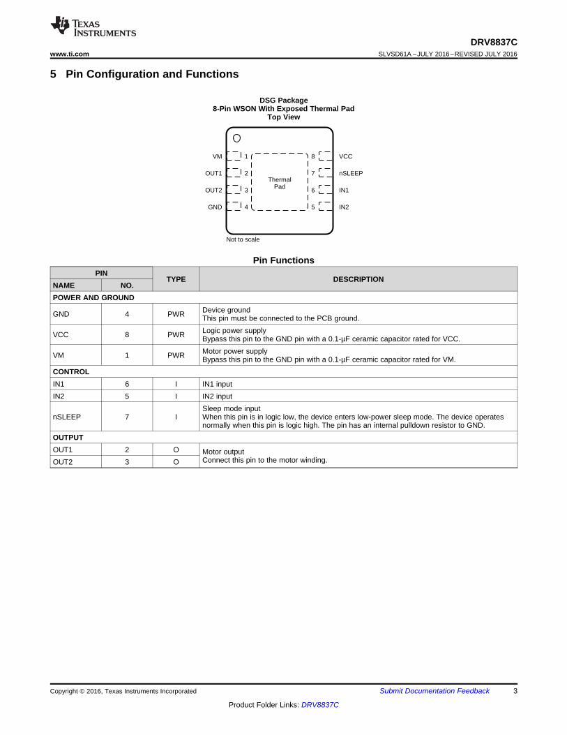
5 Pin Configuration and Functions
DSG Package8-Pin WSON With Exposed Thermal Pad
Top View
Pin FunctionsPIN
TYPE DESCRIPTIONNAME NO.POWER AND GROUND
GND 4 PWR Device groundThis pin must be connected to the PCB ground.
VCC 8 PWR Logic power supplyBypass this pin to the GND pin with a 0.1-µF ceramic capacitor rated for VCC.
VM 1 PWR Motor power supplyBypass this pin to the GND pin with a 0.1-µF ceramic capacitor rated for VM.
CONTROLIN1 6 I IN1 inputIN2 5 I IN2 input
nSLEEP 7 ISleep mode inputWhen this pin is in logic low, the device enters low-power sleep mode. The device operatesnormally when this pin is logic high. The pin has an internal pulldown resistor to GND.
OUTPUTOUT1 2 O Motor output
Connect this pin to the motor winding.OUT2 3 O

4
DRV8837CSLVSD61A –JULY 2016–REVISED JULY 2016 www.ti.com
Product Folder Links: DRV8837C
Submit Documentation Feedback Copyright © 2016, Texas Instruments Incorporated
(1) Stresses beyond those listed under Absolute Maximum Ratings may cause permanent damage to the device. These are stress ratingsonly, and functional operation of the device at these or any other conditions beyond those indicated under Recommended OperatingConditions is not implied. Exposure to absolute-maximum-rated conditions for extended periods may affect device reliability.
(2) All voltage values are with respect to network ground pin.
6 Specifications
6.1 Absolute Maximum RatingsOver operating free-air temperature range (unless otherwise noted) (1) (2)
MIN MAX UNITMotor power-supply voltage VM –0.3 12 VLogic power-supply voltage VCC –0.3 7 VControl pin voltage IN1, IN2, nSLEEP –0.5 7 VPeak drive current OUT1, OUT2 Internally limited AOperating virtual junction temperature, TJ –40 150 ºCStorage temperature, Tstg –60 150 ºC
(1) JEDEC document JEP155 states that 500-V HBM allows safe manufacturing with a standard ESD control process.(2) JEDEC document JEP157 states that 250-V CDM allows safe manufacturing with a standard ESD control process.
6.2 ESD RatingsVALUE UNIT
V(ESD)Electrostaticdischarge
Human-body model (HBM), per ANSI/ESDA/JEDEC JS-001 (1) ±4000V
Charged-device model (CDM), per JEDEC specification JESD22-C101 (2) ±1000
6.3 Recommended Operating ConditionsOver operating free-air temperature range (unless otherwise noted)
MIN MAX UNITVVM Motor power-supply voltage 0 11 VVCC Logic power-supply voltage 1.8 7 VIOUT Motor peak current 0 1 AfPWM Externally applied PWM frequency 0 250 kHzVLOGIC Logic level input voltage 0 5.5 VTA Operating ambient temperature –40 85 °C
(1) For more information about traditional and new thermal metrics, see the Semiconductor and IC Package Thermal Metrics applicationreport.
6.4 Thermal Informationover operating free-air temperature range (unless otherwise noted)
THERMAL METRIC (1)DRV8837C
UNITDSG (WSON)8 PINS
RθJA Junction-to-ambient thermal resistance 60.9 °C/WRθJC(top) Junction-to-case (top) thermal resistance 71.4 °C/WRθJB Junction-to-board thermal resistance 32.2 °C/WψJT Junction-to-top characterization parameter 1.6 °C/WψJB Junction-to-board characterization parameter 32.8 °C/WRθJC(bot) Junction-to-case (bottom) thermal resistance 9.8 °C/W

5
DRV8837Cwww.ti.com SLVSD61A –JULY 2016–REVISED JULY 2016
Product Folder Links: DRV8837C
Submit Documentation FeedbackCopyright © 2016, Texas Instruments Incorporated
(1) Not tested in production; limits are based on characterization data
6.5 Electrical CharacteristicsTA = 25°C, over recommended operating conditions unless otherwise noted
PARAMETER TEST CONDITIONS MIN TYP MAX UNITPOWER SUPPLIES (VM, VCC)VVM VM operating voltage 0 11 V
IVM VM operating supply current
VVM = 5 V; VCC = 3 V;No PWM 40 100 μA
VVM = 5 V; VCC = 3 V;50 kHz PWM 0.8 1.5 mA
IVMQ VM sleep mode supply current VVM = 5 V; VCC = 3 V;nSLEEP = 0 30 95 nA
VCC VCC operating voltage 1.8 7 V
IVCC VCC operating supply current
VVM = 5 V; VCC = 3 V;No PWM 300 500 μA
VVM = 5 V; VCC = 3 V;50 kHz PWM 0.7 1.5 mA
IVCCQ VCC sleep mode supply current VVM = 5 V; VCC = 3 V;nSLEEP = 0 5 25 nA
CONTROL INPUTS (IN1/PH, IN2/EN, nSLEEP)VIL Input logic-low voltage 0.25 × VCC VVIH Input logic-high voltage 0.5 × VCC VVHYS Input logic hysteresis 0.08 × VCC VIIL Input logic-low current VINx = 0 V –5 5 μAIIH Input logic-high current VINx = 3.3 V 50 μARPD Pulldown resistance 100 kΩMOTOR DRIVER OUTPUTS (OUT1, OUT2)
RDS(ON) HS + LS FET on-resistance VVM = 5 V; VCC = 3.3 V;IO = 200 mA; TJ = 25°C 1000 mΩ
IOFF Off-state leakage current VOUTx = 0 V –200 200 nAPROTECTION CIRCUITS
VUVLO VCC undervoltage lockoutVCC falling 1.7 VVCC rising 1.8 V
IOCP Overcurrent protection trip level 1.2 AtDEG Overcurrent deglitch time 1 μstRETRY Overcurrent retry time 1 msTTSD
(1) Thermal shutdown temperature Die temperature TJ 150 160 180 °C
z
z
z
IN2
OUT1
1 4
DRV8837C
5 6
80%
20%
80%
20%
OUTx
OUT2
IN1
z
2
3
6
DRV8837CSLVSD61A –JULY 2016–REVISED JULY 2016 www.ti.com
Product Folder Links: DRV8837C
Submit Documentation Feedback Copyright © 2016, Texas Instruments Incorporated
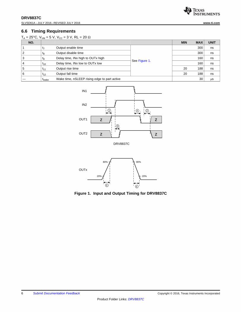
6.6 Timing RequirementsTA = 25°C, VVM = 5 V, VCC = 3 V, RL = 20 Ω
NO. MIN MAX UNIT1 t7 Output enable time
See Figure 1.
300 ns2 t8 Output disable time 300 ns3 t9 Delay time, INx high to OUTx high 160 ns4 t10 Delay time, INx low to OUTx low 160 ns5 t11 Output rise time 20 188 ns6 t12 Output fall time 20 188 ns— twake Wake time, nSLEEP rising edge to part active 30 μs
Figure 1. Input and Output Timing for DRV8837C
Ambient Temperature (°C)
RD
S(O
N) H
S+
LS (:
)
-40 -20 0 20 40 60 80 1000.5
0.75
1
1.25
1.5
1.75
2
2.25
2.5
2.75
D005
VM = 2 V, VCC = 2 VVM = 5 V, VCC = 3 VVM = 11 V, VCC = 7 V
Ambient Temperature (qC)
VM
Ope
ratin
g C
urre
nt, 5
0 kH
z P
WM
(m
A)
-40 -20 0 20 40 60 80 1000.535
0.54
0.545
0.55
0.555
0.56
0.565
0.57
0.575
D003Ambient Temperature (qC)
VC
C O
pera
ting
Cur
rent
, 50
KH
z P
WM
(m
A)
-40 -20 0 20 40 60 80 1000.44
0.46
0.48
0.5
0.52
0.54
0.56
0.58
D004
Ambient Temperature (qC)
VM
Sle
ep C
urre
nt (
nA)
-40 -20 0 20 40 60 80 10030
35
40
45
50
55
60
65
70
D001Ambient Temperature (°C)
VC
C S
leep
Cur
rent
(nA
)
-40 -20 0 20 40 60 80 1000
20
40
60
80
100
D002
7
DRV8837Cwww.ti.com SLVSD61A –JULY 2016–REVISED JULY 2016
Product Folder Links: DRV8837C
Submit Documentation FeedbackCopyright © 2016, Texas Instruments Incorporated
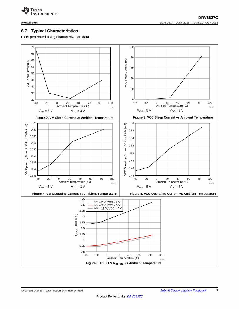
6.7 Typical CharacteristicsPlots generated using characterization data.
VVM = 5 V VCC = 3 V
Figure 2. VM Sleep Current vs Ambient Temperature
VVM = 5 V VCC = 3 V
Figure 3. VCC Sleep Current vs Ambient Temperature
VVM = 5 V VCC = 3 V
Figure 4. VM Operating Current vs Ambient Temperature
VVM = 5 V VCC = 3 V
Figure 5. VCC Operating Current vs Ambient Temperature
Figure 6. HS + LS RDS(ON) vs Ambient Temperature
VMPower
Logic
Charge Pump
VM
OUT1
nSLEEP
VM
IN1
IN2
GND PPAD
Gate Drive
VM
OUT2Gate Drive
BDCCore Logic
Control Inputs
Overcurrent
Undervoltage
Thermal
VCC
VCC
BDC
Copyright © 2016, Texas Instruments Incorporated
8
DRV8837CSLVSD61A –JULY 2016–REVISED JULY 2016 www.ti.com
Product Folder Links: DRV8837C
Submit Documentation Feedback Copyright © 2016, Texas Instruments Incorporated
7 Detailed Description
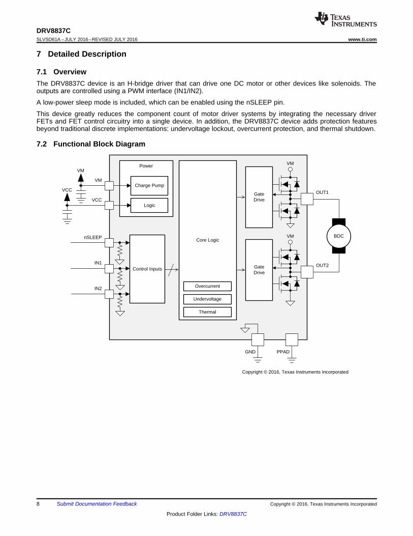
7.1 OverviewThe DRV8837C device is an H-bridge driver that can drive one DC motor or other devices like solenoids. Theoutputs are controlled using a PWM interface (IN1/IN2).
A low-power sleep mode is included, which can be enabled using the nSLEEP pin.
This device greatly reduces the component count of motor driver systems by integrating the necessary driverFETs and FET control circuitry into a single device. In addition, the DRV8837C device adds protection featuresbeyond traditional discrete implementations: undervoltage lockout, overcurrent protection, and thermal shutdown.
7.2 Functional Block Diagram

9
DRV8837Cwww.ti.com SLVSD61A –JULY 2016–REVISED JULY 2016
Product Folder Links: DRV8837C
Submit Documentation FeedbackCopyright © 2016, Texas Instruments Incorporated
7.3 Feature Description
7.3.1 Bridge ControlThe DRV8837C device is controlled using a PWM input interface, also called an IN/IN interface. Each output iscontrolled by a corresponding input pin.
Table 1 shows the logic for the DRV8837C device.
Table 1. DRV8837C Device LogicnSLEEP IN1 IN2 OUT1 OUT2 FUNCTION (DC MOTOR)
0 X X Z Z Coast1 0 0 Z Z Coast1 0 1 L H Reverse1 1 0 H L Forward1 1 1 L L Brake
7.3.2 Sleep ModeIf the nSLEEP pin is brought to a logic-low state, the DRV8837C device enters a low-power sleep mode. In thisstate, all unnecessary internal circuitry is powered down.
7.3.3 Power Supplies and Input PinsThe input pins can be driven within the recommended operating conditions with or without the VCC, VM, or bothpower supplies present. No leakage current path exists to the supply. Each input pin has a weak pulldownresistor (approximately 100 kΩ) to ground.
The VCC and VM supplies can be applied and removed in any order. When the VCC supply is removed, thedevice enters a low-power state and draws very little current from the VM supply. The VCC and VM pins can beconnected together if the supply voltage is between 1.8 and 7 V.
The VM voltage supply does not have any undervoltage-lockout protection (UVLO). As long as VCC > 1.8 V, theinternal device logic remains active which means that the VM pin voltage can drop to 0 V, however, the load maynot be sufficiently driven at low VM voltages.
7.3.4 Protection CircuitsThe DRV8837C is fully protected against VCC undervoltage, overcurrent, and overtemperature events.
VCC undervoltage lockout If at any time the voltage on the VCC pin falls below the undervoltage lockoutthreshold voltage, all FETs in the H-bridge are disabled. Operation resumes when the VCC pinvoltage rises above the UVLO threshold.
Overcurrent protection (OCP) An analog current-limit circuit on each FET limits the current through the FET byremoving the gate drive. If this analog current limit persists for longer than tDEG, all FETs in the H-bridge are disabled. Operation resumes automatically after tRETRY has elapsed. Overcurrentconditions are detected on both the high-side and low-side devices. A short to the VM pin, GND, orfrom the OUT1 pin to theOUT2 pin results in an overcurrent condition.
Thermal shutdown (TSD) If the die temperature exceeds safe limits, all FETs in the H-bridge are disabled. Afterthe die temperature falls to a safe level, operation automatically resumes.
Table 2. Fault BehaviorFAULT CONDITION H-BRIDGE RECOVERY
VCC undervoltage (UVLO) VCC < 1.7 V Disabled VCC > 1.8 VOvercurrent (OCP) IOUT > 1.2 A (MIN) Disabled (retries
automatically)tRETRY elapses
Thermal Shutdown (TSD) TJ > 150°C (MIN) Disabled (retriesautomatically)
TJ < 150°C
10
DRV8837CSLVSD61A –JULY 2016–REVISED JULY 2016 www.ti.com
Product Folder Links: DRV8837C
Submit Documentation Feedback Copyright © 2016, Texas Instruments Incorporated
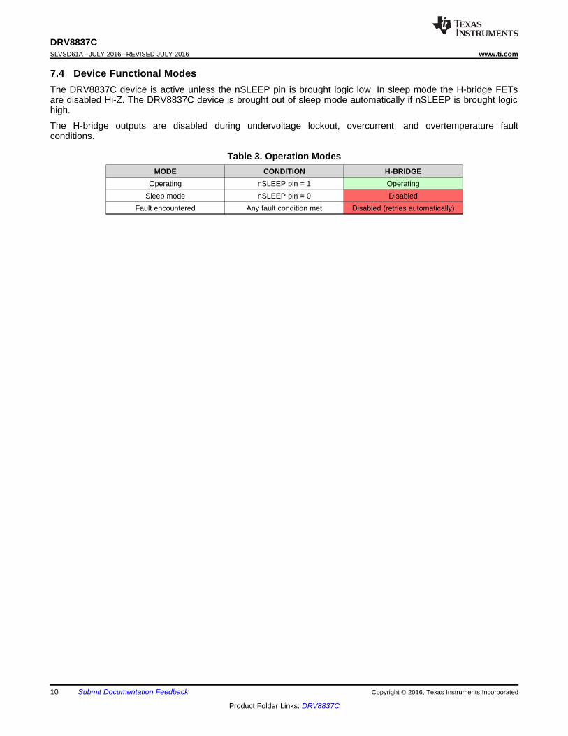
7.4 Device Functional ModesThe DRV8837C device is active unless the nSLEEP pin is brought logic low. In sleep mode the H-bridge FETsare disabled Hi-Z. The DRV8837C device is brought out of sleep mode automatically if nSLEEP is brought logichigh.
The H-bridge outputs are disabled during undervoltage lockout, overcurrent, and overtemperature faultconditions.
Table 3. Operation ModesMODE CONDITION H-BRIDGE
Operating nSLEEP pin = 1 OperatingSleep mode nSLEEP pin = 0 Disabled
Fault encountered Any fault condition met Disabled (retries automatically)

VM
OUT1
OUT2
GND
VCC
nSLEEP
IN1
IN2
8
7
6
5
1
2
3
4
DRV8837C
The
rmal
Pad
M
VCC
0.1 µF
VM
0.1 µF
Copyright © 2016, Texas Instruments Incorporated
11
DRV8837Cwww.ti.com SLVSD61A –JULY 2016–REVISED JULY 2016
Product Folder Links: DRV8837C
Submit Documentation FeedbackCopyright © 2016, Texas Instruments Incorporated
8 Application and Implementation
NOTEInformation in the following applications sections is not part of the TI componentspecification, and TI does not warrant its accuracy or completeness. TI’s customers areresponsible for determining suitability of components for their purposes. Customers shouldvalidate and test their design implementation to confirm system functionality.
8.1 Application InformationThe DRV8837C device is device is used to drive one DC motor or other devices like solenoids. The followingdesign procedure can be used to configure the DRV8837C device.
8.2 Typical Application
Figure 7. Schematic of DRV8837C Application
8.2.1 Design RequirementsTable 4 lists the required parameters for a typical usage case.
Table 4. System Design RequirementsDESIGN PARAMETER REFERENCE EXAMPLE VALUE
Motor supply voltage VM 9 VLogic supply voltage VCC 3.3 VTarget RMS current IOUT 0.8 A
8.2.2 Detailed Design Procedure
8.2.2.1 Motor VoltageThe appropriate motor voltage depends on the ratings of the motor selected and the desired RPM. A highervoltage spins a brushed dc motor faster with the same PWM duty cycle applied to the power FETs. A highervoltage also increases the rate of current change through the inductive motor windings.
8.2.2.2 Low-Power OperationWhen entering sleep mode, TI recommends setting all inputs as a logic low to minimize system power.
12
DRV8837CSLVSD61A –JULY 2016–REVISED JULY 2016 www.ti.com
Product Folder Links: DRV8837C
Submit Documentation Feedback Copyright © 2016, Texas Instruments Incorporated
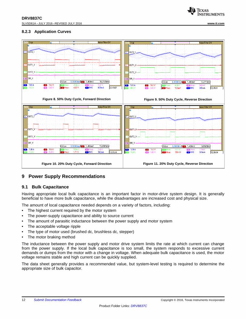
8.2.3 Application Curves
Figure 8. 50% Duty Cycle, Forward Direction Figure 9. 50% Duty Cycle, Reverse Direction
Figure 10. 20% Duty Cycle, Forward Direction Figure 11. 20% Duty Cycle, Reverse Direction
9 Power Supply Recommendations
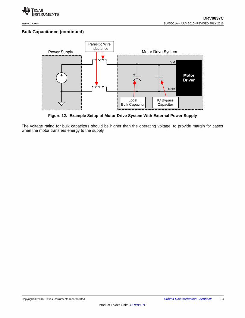
9.1 Bulk CapacitanceHaving appropriate local bulk capacitance is an important factor in motor-drive system design. It is generallybeneficial to have more bulk capacitance, while the disadvantages are increased cost and physical size.
The amount of local capacitance needed depends on a variety of factors, including:• The highest current required by the motor system• The power-supply capacitance and ability to source current• The amount of parasitic inductance between the power supply and motor system• The acceptable voltage ripple• The type of motor used (brushed dc, brushless dc, stepper)• The motor braking method
The inductance between the power supply and motor drive system limits the rate at which current can changefrom the power supply. If the local bulk capacitance is too small, the system responds to excessive currentdemands or dumps from the motor with a change in voltage. When adequate bulk capacitance is used, the motorvoltage remains stable and high current can be quickly supplied.
The data sheet generally provides a recommended value, but system-level testing is required to determine theappropriate size of bulk capacitor.
Local
Bulk Capacitor
Parasitic Wire
Inductance
+–
Motor
Driver
Power Supply Motor Drive System
VM
GND
+
IC Bypass
Capacitor
13
DRV8837Cwww.ti.com SLVSD61A –JULY 2016–REVISED JULY 2016
Product Folder Links: DRV8837C
Submit Documentation FeedbackCopyright © 2016, Texas Instruments Incorporated
Bulk Capacitance (continued)
Figure 12. Example Setup of Motor Drive System With External Power Supply
The voltage rating for bulk capacitors should be higher than the operating voltage, to provide margin for caseswhen the motor transfers energy to the supply
2TOT DS(ON) OUT(RMS)P R (I )= ´
0.1 µF
VCC
SLEEPn
IN1
IN2
VM
OUT1
OUT2
GND
0.1 µF
14
DRV8837CSLVSD61A –JULY 2016–REVISED JULY 2016 www.ti.com
Product Folder Links: DRV8837C
Submit Documentation Feedback Copyright © 2016, Texas Instruments Incorporated
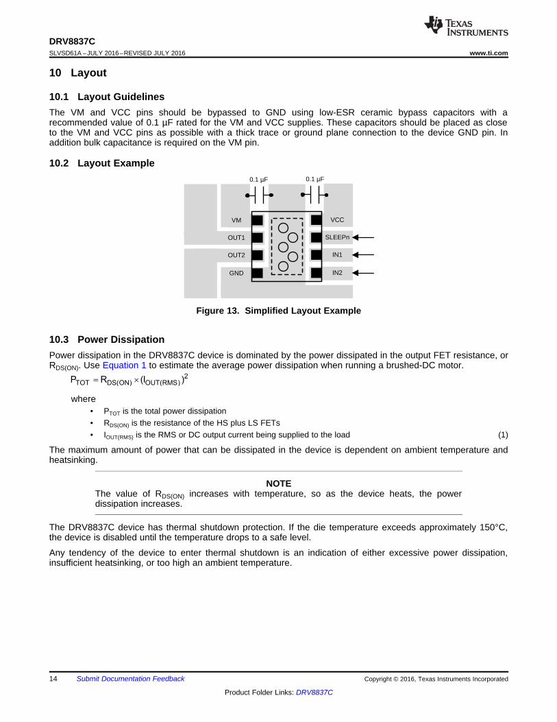
10 Layout
10.1 Layout GuidelinesThe VM and VCC pins should be bypassed to GND using low-ESR ceramic bypass capacitors with arecommended value of 0.1 µF rated for the VM and VCC supplies. These capacitors should be placed as closeto the VM and VCC pins as possible with a thick trace or ground plane connection to the device GND pin. Inaddition bulk capacitance is required on the VM pin.
10.2 Layout Example
Figure 13. Simplified Layout Example
10.3 Power DissipationPower dissipation in the DRV8837C device is dominated by the power dissipated in the output FET resistance, orRDS(ON). Use Equation 1 to estimate the average power dissipation when running a brushed-DC motor.
where• PTOT is the total power dissipation• RDS(ON) is the resistance of the HS plus LS FETs• IOUT(RMS) is the RMS or DC output current being supplied to the load (1)
The maximum amount of power that can be dissipated in the device is dependent on ambient temperature andheatsinking.
NOTEThe value of RDS(ON) increases with temperature, so as the device heats, the powerdissipation increases.
The DRV8837C device has thermal shutdown protection. If the die temperature exceeds approximately 150°C,the device is disabled until the temperature drops to a safe level.
Any tendency of the device to enter thermal shutdown is an indication of either excessive power dissipation,insufficient heatsinking, or too high an ambient temperature.
15
DRV8837Cwww.ti.com SLVSD61A –JULY 2016–REVISED JULY 2016
Product Folder Links: DRV8837C
Submit Documentation FeedbackCopyright © 2016, Texas Instruments Incorporated
11 Device and Documentation Support
11.1 Documentation Support
11.1.1 Related DocumentationFor related documentation see the following:• Calculating Motor Driver Power Dissipation (SLVA504)• DRV8837C Evaluation Module User's Guide (SLVUAS3)• Understanding Motor Driver Current Ratings (SLVA505)
11.2 Receiving Notification of Documentation UpdatesTo receive notification of documentation updates, navigate to the device product folder on ti.com. In the upperright corner, click on Alert me to register and receive a weekly digest of any product information that haschanged. For change details, review the revision history included in any revised document.
11.3 Community ResourcesThe following links connect to TI community resources. Linked contents are provided "AS IS" by the respectivecontributors. They do not constitute TI specifications and do not necessarily reflect TI's views; see TI's Terms ofUse.
TI E2E™ Online Community TI's Engineer-to-Engineer (E2E) Community. Created to foster collaborationamong engineers. At e2e.ti.com, you can ask questions, share knowledge, explore ideas and helpsolve problems with fellow engineers.
Design Support TI's Design Support Quickly find helpful E2E forums along with design support tools andcontact information for technical support.
11.4 TrademarksE2E is a trademark of Texas Instruments.All other trademarks are the property of their respective owners.
11.5 Electrostatic Discharge CautionThis integrated circuit can be damaged by ESD. Texas Instruments recommends that all integrated circuits be handled withappropriate precautions. Failure to observe proper handling and installation procedures can cause damage.
ESD damage can range from subtle performance degradation to complete device failure. Precision integrated circuits may be moresusceptible to damage because very small parametric changes could cause the device not to meet its published specifications.
11.6 GlossarySLYZ022 — TI Glossary.
This glossary lists and explains terms, acronyms, and definitions.
12 Mechanical, Packaging, and Orderable InformationThe following pages include mechanical, packaging, and orderable information. This information is the mostcurrent data available for the designated devices. This data is subject to change without notice and revision ofthis document. For browser-based versions of this data sheet, refer to the left-hand navigation.

PACKAGE OPTION ADDENDUM
www.ti.com 10-Dec-2020
Addendum-Page 1
PACKAGING INFORMATION
Orderable Device Status(1)
Package Type PackageDrawing
Pins PackageQty
Eco Plan(2)
Lead finish/Ball material
(6)
MSL Peak Temp(3)
Op Temp (°C) Device Marking(4/5)
Samples
DRV8837CDSGR ACTIVE WSON DSG 8 3000 RoHS & Green NIPDAU Level-2-260C-1 YEAR -40 to 85 837C
DRV8837CDSGT ACTIVE WSON DSG 8 250 RoHS & Green NIPDAU Level-2-260C-1 YEAR -40 to 85 837C
(1) The marketing status values are defined as follows:ACTIVE: Product device recommended for new designs.LIFEBUY: TI has announced that the device will be discontinued, and a lifetime-buy period is in effect.NRND: Not recommended for new designs. Device is in production to support existing customers, but TI does not recommend using this part in a new design.PREVIEW: Device has been announced but is not in production. Samples may or may not be available.OBSOLETE: TI has discontinued the production of the device.
(2) RoHS: TI defines "RoHS" to mean semiconductor products that are compliant with the current EU RoHS requirements for all 10 RoHS substances, including the requirement that RoHS substancedo not exceed 0.1% by weight in homogeneous materials. Where designed to be soldered at high temperatures, "RoHS" products are suitable for use in specified lead-free processes. TI mayreference these types of products as "Pb-Free".RoHS Exempt: TI defines "RoHS Exempt" to mean products that contain lead but are compliant with EU RoHS pursuant to a specific EU RoHS exemption.Green: TI defines "Green" to mean the content of Chlorine (Cl) and Bromine (Br) based flame retardants meet JS709B low halogen requirements of <=1000ppm threshold. Antimony trioxide basedflame retardants must also meet the <=1000ppm threshold requirement.
(3) MSL, Peak Temp. - The Moisture Sensitivity Level rating according to the JEDEC industry standard classifications, and peak solder temperature.
(4) There may be additional marking, which relates to the logo, the lot trace code information, or the environmental category on the device.
(5) Multiple Device Markings will be inside parentheses. Only one Device Marking contained in parentheses and separated by a "~" will appear on a device. If a line is indented then it is a continuationof the previous line and the two combined represent the entire Device Marking for that device.
(6) Lead finish/Ball material - Orderable Devices may have multiple material finish options. Finish options are separated by a vertical ruled line. Lead finish/Ball material values may wrap to twolines if the finish value exceeds the maximum column width.
Important Information and Disclaimer:The information provided on this page represents TI's knowledge and belief as of the date that it is provided. TI bases its knowledge and belief on informationprovided by third parties, and makes no representation or warranty as to the accuracy of such information. Efforts are underway to better integrate information from third parties. TI has taken andcontinues to take reasonable steps to provide representative and accurate information but may not have conducted destructive testing or chemical analysis on incoming materials and chemicals.TI and TI suppliers consider certain information to be proprietary, and thus CAS numbers and other limited information may not be available for release.
In no event shall TI's liability arising out of such information exceed the total purchase price of the TI part(s) at issue in this document sold by TI to Customer on an annual basis.

PACKAGE OPTION ADDENDUM
www.ti.com 10-Dec-2020
Addendum-Page 2
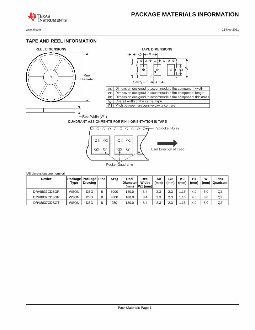
TAPE AND REEL INFORMATION
*All dimensions are nominal
Device PackageType
PackageDrawing
Pins SPQ ReelDiameter
(mm)
ReelWidth
W1 (mm)
A0(mm)
B0(mm)
K0(mm)
P1(mm)
W(mm)
Pin1Quadrant
DRV8837CDSGR WSON DSG 8 3000 180.0 8.4 2.3 2.3 1.15 4.0 8.0 Q2
DRV8837CDSGR WSON DSG 8 3000 180.0 8.4 2.3 2.3 1.15 4.0 8.0 Q2
DRV8837CDSGT WSON DSG 8 250 180.0 8.4 2.3 2.3 1.15 4.0 8.0 Q2
PACKAGE MATERIALS INFORMATION
www.ti.com 11-Nov-2021
Pack Materials-Page 1

*All dimensions are nominal
Device Package Type Package Drawing Pins SPQ Length (mm) Width (mm) Height (mm)
DRV8837CDSGR WSON DSG 8 3000 210.0 185.0 35.0
DRV8837CDSGR WSON DSG 8 3000 210.0 185.0 35.0
DRV8837CDSGT WSON DSG 8 250 210.0 185.0 35.0
PACKAGE MATERIALS INFORMATION
www.ti.com 11-Nov-2021
Pack Materials-Page 2
www.ti.com
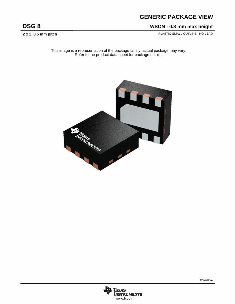
GENERIC PACKAGE VIEW
This image is a representation of the package family, actual package may vary.Refer to the product data sheet for package details.
WSON - 0.8 mm max heightDSG 8PLASTIC SMALL OUTLINE - NO LEAD2 x 2, 0.5 mm pitch
4224783/A

www.ti.com
PACKAGE OUTLINE
C
8X 0.320.18
1.6 0.12X1.5
0.9 0.1
6X 0.5
8X 0.40.2
0.050.00
0.8 MAX
A 2.11.9
B
2.11.9
0.320.18
0.40.2
(0.2) TYP
WSON - 0.8 mm max heightDSG0008APLASTIC SMALL OUTLINE - NO LEAD
4218900/D 04/2020
PIN 1 INDEX AREA
SEATING PLANE
0.08 C
1
4 5
8
PIN 1 ID0.1 C A B0.05 C
THERMAL PADEXPOSED
9
NOTES: 1. All linear dimensions are in millimeters. Any dimensions in parenthesis are for reference only. Dimensioning and tolerancing per ASME Y14.5M. 2. This drawing is subject to change without notice. 3. The package thermal pad must be soldered to the printed circuit board for thermal and mechanical performance.
SCALE 5.500
ALTERNATIVE TERMINAL SHAPETYPICAL
www.ti.com
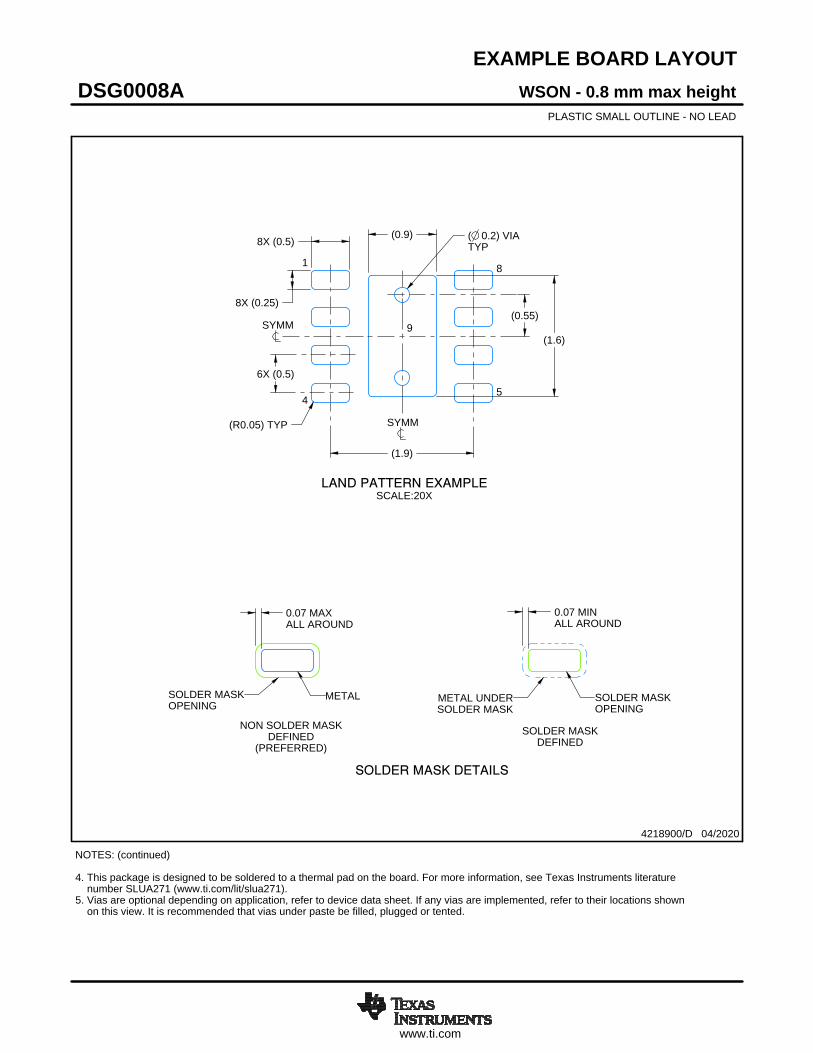
EXAMPLE BOARD LAYOUT
0.07 MINALL AROUND
0.07 MAXALL AROUND
8X (0.25)
(1.6)
(1.9)
6X (0.5)
(0.9) ( 0.2) VIATYP
(0.55)
8X (0.5)
(R0.05) TYP
WSON - 0.8 mm max heightDSG0008APLASTIC SMALL OUTLINE - NO LEAD
4218900/D 04/2020
SYMM
1
45
8
LAND PATTERN EXAMPLESCALE:20X
SYMM 9
NOTES: (continued) 4. This package is designed to be soldered to a thermal pad on the board. For more information, see Texas Instruments literature number SLUA271 (www.ti.com/lit/slua271).5. Vias are optional depending on application, refer to device data sheet. If any vias are implemented, refer to their locations shown on this view. It is recommended that vias under paste be filled, plugged or tented.
SOLDER MASKOPENINGSOLDER MASK
METAL UNDER
SOLDER MASKDEFINED
METALSOLDER MASKOPENING
SOLDER MASK DETAILS
NON SOLDER MASKDEFINED
(PREFERRED)
www.ti.com
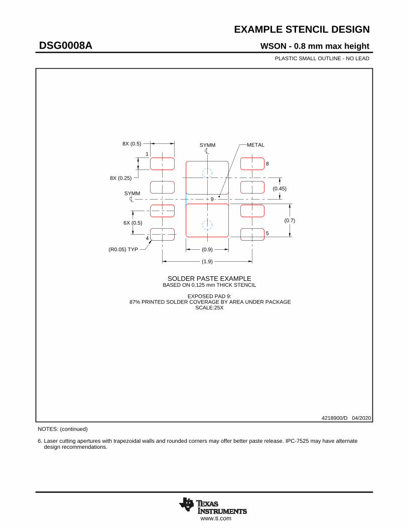
EXAMPLE STENCIL DESIGN
(R0.05) TYP
8X (0.25)
8X (0.5)
(0.9)
(0.7)
(1.9)
(0.45)
6X (0.5)
WSON - 0.8 mm max heightDSG0008APLASTIC SMALL OUTLINE - NO LEAD
4218900/D 04/2020
NOTES: (continued) 6. Laser cutting apertures with trapezoidal walls and rounded corners may offer better paste release. IPC-7525 may have alternate design recommendations.
SOLDER PASTE EXAMPLEBASED ON 0.125 mm THICK STENCIL
EXPOSED PAD 9:
87% PRINTED SOLDER COVERAGE BY AREA UNDER PACKAGESCALE:25X
SYMM1
45
8
METAL
SYMM9

IMPORTANT NOTICE AND DISCLAIMERTI PROVIDES TECHNICAL AND RELIABILITY DATA (INCLUDING DATA SHEETS), DESIGN RESOURCES (INCLUDING REFERENCE DESIGNS), APPLICATION OR OTHER DESIGN ADVICE, WEB TOOLS, SAFETY INFORMATION, AND OTHER RESOURCES “AS IS” AND WITH ALL FAULTS, AND DISCLAIMS ALL WARRANTIES, EXPRESS AND IMPLIED, INCLUDING WITHOUT LIMITATION ANY IMPLIED WARRANTIES OF MERCHANTABILITY, FITNESS FOR A PARTICULAR PURPOSE OR NON-INFRINGEMENT OF THIRD PARTY INTELLECTUAL PROPERTY RIGHTS.These resources are intended for skilled developers designing with TI products. You are solely responsible for (1) selecting the appropriate TI products for your application, (2) designing, validating and testing your application, and (3) ensuring your application meets applicable standards, and any other safety, security, regulatory or other requirements.These resources are subject to change without notice. TI grants you permission to use these resources only for development of an application that uses the TI products described in the resource. Other reproduction and display of these resources is prohibited. No license is granted to any other TI intellectual property right or to any third party intellectual property right. TI disclaims responsibility for, and you will fully indemnify TI and its representatives against, any claims, damages, costs, losses, and liabilities arising out of your use of these resources.TI’s products are provided subject to TI’s Terms of Sale or other applicable terms available either on ti.com or provided in conjunction with such TI products. TI’s provision of these resources does not expand or otherwise alter TI’s applicable warranties or warranty disclaimers for TI products.TI objects to and rejects any additional or different terms you may have proposed. IMPORTANT NOTICE
Mailing Address: Texas Instruments, Post Office Box 655303, Dallas, Texas 75265Copyright © 2021, Texas Instruments Incorporated