dsp processor core-based wireless system design
TRANSCRIPT

Mika Kuulusa
Tampereen teknillinen korkeakouluJulkaisuja 296
Tampere University of TechnologyPublications 296
Tampere 2000
DSP Processor Core-Based Wireless System Design
Mika Kuulusa
DSP Processor Core-Based Wireless System Design
Dr.Tech. Thesis, 156 pages18th August 2000
Contact Information:
Mika Kuulusa
Tampere University of Technology
Digital and Computer Systems Laboratory
P.O.Box 553
33101 TAMPERE
Tel: 03 – 365 3872 work, 040 – 727 5512 mobile
Fax: 03 – 365 3095 work
E-mail: [email protected]
ABSTRACT
This thesis considers the design of wireless communications systems which are implemented
as highly integrated embedded systems comprised of a mixture of hardware components and
software. An introductionary part presents digital communications systems, classification of
processors, programmable digital signal processing (DSP) processors, and development and
implementation of a flexible DSP processor architecture. This introduction is followed by a
total of seven publications comprising the research work. In this thesis the following topics
have been considered.
Most of the presented research work is based on a customizable fixed-point DSP processor
which has been implemented as a highly optimized hard core for use in typical DSP
applications. The studied topics cover a plethora of aspects starting from the initial
development of the processor architecture. Several real-time DSP applications, such as
MPEG audio decoding and GSM speech coding, have been developed and their performance
with this particular processor have been evaluated.
The processor core itself as a bare hardware circuit is not usable without various software
tools, function libraries, a C-compiler, and a real-time operating system. The set of
development tools was gradually refined and several architectural enhancements were
implemented during further development of the initial processor core. Furthermore, the
modified Harvard memory architecture with one program memory bank was replaced with a
parallel program memory architecture. With this architecture the processor accesses several
instructions in parallel to compensate for a potentially slow read access time, a characteristic
which is typical of, for example, flash memory devices.
The development flow for heterogenous hardware/software systems is also studied. As
a case study, a configurable hardware block performing two trigonometric transforms
was embedded into a wireless LAN system described as a dataflow graph. Furthermore,
implementation aspects of an emerging communications system were studied. A high-level
feasibility study of a W-CDMA radio transceiver for a mobile terminal was carried out to
serve as a justification for partitioning various baseband functions into application-specific
hardware units and DSP software to be executed on a programmable DSP processor.

PREFACE
The research work described in this thesis was carried out during the years 1996 – 2000
in the Digital and Computer Systems Laboratory at the Tampere University of Technology,
Tampere, Finland.
I would like to express my warmest gratitude to my thesis advisor, Prof. Jari Nurmi,
for his skillful guidance and support during the course of the research work. I gratefully
acknowledge the research support received from Prof. Jarkko Niittylahti and Prof. Jukka
Saarinen, the head of the laboratory. In particular I am indebted to my background mentor,
Prof. Jarmo Takala, whose encouragement and open-hearted support have had a significant
role in making this thesis a reality. I would also like to thank Teemu Parkkinen, M.Sc., for
our constructive teamwork. Moreover, I express sincere thanks to my dear colleagues for
their valuable assistance and for making the atmosphere at the laboratory so inspiring and
innovative. I would also like to thank Prof. Jorma Skytta and Jarno Knuutila, Dr.Tech, for
their constructive feedback and comments on the manuscript.
During the past years I have had the utmost pleasure of working in collaboration with VLSI
Solution and Nokia Research Center, both in Tampere, Finland. I have had the privilege
to work with the talented silicon architects at VLSI Solution. I would like to express my
sincere gratitude to Prof. Jari Nurmi and Tapani Ritoniemi, M.Sc., for providing me with
this exceptional opportunity. In addition I would like to thank Janne Takala, M.Sc., Pasi
Ojala, M.Sc., Juha Rostrom, M.Sc., and Henrik Herranen for their enthusiastic support.
Furthermore, it has been a great pleasure to work with the people at Nokia Research Center.
In particular, the numerous technical sessions and workshops have been both exciting and
fruitful.
The research work was financially supported by the National Technology Agency (TEKES),
Tampere Graduate School in Information Science and Engineering (TISE), and Tampere
University of Technology. Moreover, I gratefully acknowledge the research grants received
from the Ulla Tuominen Foundation, the Jenny and Antti Wihuri Foundation, the Foundation
of Finnish Electronics Engineers, the Foundation of Advancement of Technology, the
Foundation of Advancement of Telecommunications, and the Finnish Cultural Foundation.

iv Preface
Most of all I wish to express my deepest gratitude to my parents Vesa and Paula Kuulusa,
my brother Juha, and my sister Nina for their love, encouragement, and compassion during
all these years. Without their full support it would not have been possible to accomplish this
long-spanning project.
Tampere, August 2000
Mika Kuulusa
TABLE OF CONTENTS
Abstract . . . . . . . . . . . . . . . . . . . . . . . . . . . . . . . . . . . . . . . . i
Preface . . . . . . . . . . . . . . . . . . . . . . . . . . . . . . . . . . . . . . . . . iii
Table of Contents . . . . . . . . . . . . . . . . . . . . . . . . . . . . . . . . . . . v
List of Publications . . . . . . . . . . . . . . . . . . . . . . . . . . . . . . . . . . vii
List of Figures . . . . . . . . . . . . . . . . . . . . . . . . . . . . . . . . . . . . . ix
List of Tables . . . . . . . . . . . . . . . . . . . . . . . . . . . . . . . . . . . . . xi
List of Abbreviations . . . . . . . . . . . . . . . . . . . . . . . . . . . . . . . . . . xiii
Part I Introduction 1
1. Introduction to Thesis . . . . . . . . . . . . . . . . . . . . . . . . . . . . . . . 3
1.1 Objectives of Research . . . . . . . . . . . . . . . . . . . . . . . . . . . . 3
1.2 Outline of Thesis . . . . . . . . . . . . . . . . . . . . . . . . . . . . . . . 4
2. Wireless Communications System Design . . . . . . . . . . . . . . . . . . . . . 5
2.1 Digital Signal Processing . . . . . . . . . . . . . . . . . . . . . . . . . . . 5
2.2 Wireless Communications Systems . . . . . . . . . . . . . . . . . . . . . . 6
2.3 Wireless System Design . . . . . . . . . . . . . . . . . . . . . . . . . . . 9
2.3.1 System Design Flow . . . . . . . . . . . . . . . . . . . . . . . . . 9
2.3.2 Processor Core-Based Design . . . . . . . . . . . . . . . . . . . . 12
3. Programmable Processor Architectures . . . . . . . . . . . . . . . . . . . . . . 15
3.1 Instruction-Set Architectures . . . . . . . . . . . . . . . . . . . . . . . . . 15
3.1.1 Memory Organization . . . . . . . . . . . . . . . . . . . . . . . . 16
3.1.2 Operand Location . . . . . . . . . . . . . . . . . . . . . . . . . . . 17
3.1.3 Memory Addressing . . . . . . . . . . . . . . . . . . . . . . . . . 17
vi Table of Contents
3.1.4 Number Systems . . . . . . . . . . . . . . . . . . . . . . . . . . . 18
3.2 Enhancing Processor Performance . . . . . . . . . . . . . . . . . . . . . . 19
3.2.1 Pipelining . . . . . . . . . . . . . . . . . . . . . . . . . . . . . . . 19
3.2.2 Instruction-Level Parallelism . . . . . . . . . . . . . . . . . . . . . 20
3.2.3 Data-Level Parallelism . . . . . . . . . . . . . . . . . . . . . . . . 22
3.2.4 Task-Level Parallelism . . . . . . . . . . . . . . . . . . . . . . . . 23
4. Programmable DSP Processors . . . . . . . . . . . . . . . . . . . . . . . . . . 25
4.1 Historical Perspective . . . . . . . . . . . . . . . . . . . . . . . . . . . . . 25
4.2 Fundamentals . . . . . . . . . . . . . . . . . . . . . . . . . . . . . . . . . 26
4.3 Conventional DSP Processors . . . . . . . . . . . . . . . . . . . . . . . . . 28
4.4 VLIW DSP Processors . . . . . . . . . . . . . . . . . . . . . . . . . . . . 32
5. Customizable Fixed-Point DSP Processor Core . . . . . . . . . . . . . . . . . . 35
5.1 Background . . . . . . . . . . . . . . . . . . . . . . . . . . . . . . . . . . 35
5.2 Architecture . . . . . . . . . . . . . . . . . . . . . . . . . . . . . . . . . . 35
5.2.1 Program Control Unit . . . . . . . . . . . . . . . . . . . . . . . . 37
5.2.2 Datapath . . . . . . . . . . . . . . . . . . . . . . . . . . . . . . . 40
5.2.3 Data Address Generator . . . . . . . . . . . . . . . . . . . . . . . 41
5.3 Implementation . . . . . . . . . . . . . . . . . . . . . . . . . . . . . . . . 42
5.3.1 Processor Hardware . . . . . . . . . . . . . . . . . . . . . . . . . 42
5.3.2 Software Tools . . . . . . . . . . . . . . . . . . . . . . . . . . . . 46
6. Summary of Publications . . . . . . . . . . . . . . . . . . . . . . . . . . . . . 49
6.1 Customizable Fixed-Point DSP Processor Core . . . . . . . . . . . . . . . 49
6.2 Specification of Wireless Communications Systems . . . . . . . . . . . . . 51
6.3 Author’s Contribution to Published Work . . . . . . . . . . . . . . . . . . 52
7. Conclusions . . . . . . . . . . . . . . . . . . . . . . . . . . . . . . . . . . . . 55
7.1 Main Results . . . . . . . . . . . . . . . . . . . . . . . . . . . . . . . . . 55
7.2 Future Trends . . . . . . . . . . . . . . . . . . . . . . . . . . . . . . . . . 58
Bibliography . . . . . . . . . . . . . . . . . . . . . . . . . . . . . . . . . . . . . . 61
Part II Publications 75
LIST OF PUBLICATIONS
This thesis is divided into two parts. Part I has an introduction to the scope of the research
work covered by the thesis. Part II contains reprints of the related publications. In the text
these publications are referred to as [P1], [P2], . . . , [P7].
[P1] M. Kuulusa and J. Nurmi, “A parameterized and extensible DSP core architecture,”
in Proc. Int. Symposium on IC Technology, Systems & Applications, Singapore, Sep.
10–12 1997, pp. 414–417.
[P2] M. Kuulusa, J. Nurmi, J. Takala, P. Ojala, and H. Herranen, “Flexible DSP core for
embedded systems,” IEEE Design & Test of Computers, vol. 14, no. 4, pp. 60–68,
Oct./Dec. 1997.
[P3] M. Kuulusa, T. Parkkinen, and J. Niittylahti, “MPEG-1 layer II audio decoder
implementation for a parameterized DSP core,” in Proc. Int. Conference on Signal
Processing Applications and Technology, Orlando, FL, U.S.A., Nov. 1–4 1999
(CD-ROM).
[P4] M. Kuulusa, J. Nurmi, and J. Niittylahti, “A parallel program memory architecture
for a DSP,” in Proc. Int. Symposium on Integrated Circuits, Devices & Systems,
Singapore, Sep. 10–12 1999, pp. 475–479.
[P5] J. Takala, M. Kuulusa, P. Ojala, and J. Nurmi, “Enhanced DSP core for embedded
applications,” in Proc. Int. Workshop on Signal Processing Systems: Design and
Implementation, Taipei, Taiwan, Oct. 20–22 1999, pp. 271–280.
[P6] M. Kuulusa, J. Takala, and J. Saarinen, “Run-time configurable hardware model
in a dataflow simulation,” in Proc. IEEE Asia-Pacific Conference on Circuits and
Systems, Chiangmai, Thailand, Nov. 24–27 1998, pp. 763–766.
[P7] M. Kuulusa and J. Nurmi, “Baseband implementation aspects for W-CDMA
mobile terminals,” in Proc. Baiona Workshop on Emerging Technologies in
Telecommunications, Baiona, Spain, Sep. 6–8 1999, pp. 292–296.

LIST OF FIGURES
1 Block diagram of a simplified, generalized DSP system . . . . . . . . . . . 6
2 Functional block diagram of a wireless communications system . . . . . . 7
3 Functional block diagram of a W-CDMA transceiver for mobile terminals . 8
4 System-level design process of embedded systems . . . . . . . . . . . . . . 10
5 Example of an integrated DECT communications platform . . . . . . . . . 12
6 Classification of processor memory architectures . . . . . . . . . . . . . . 16
7 Common data memory addressing modes . . . . . . . . . . . . . . . . . . 18
8 Illustration of instruction issue mechanisms in processors . . . . . . . . . . 21
9 Illustration of two SIMD instructions . . . . . . . . . . . . . . . . . . . . . 23
10 Block diagram of an integrated cellular baseband processor . . . . . . . . . 24
11 Example of an assembly source code implementing a 64-tap FIR filter . . . 27
12 Simplified block diagrams of two conventional DSP processors . . . . . . . 30
13 Simplified block diagrams of two VLIW DSP processors . . . . . . . . . . 33
14 Base architecture of the customizable fixed-point DSP processor . . . . . . 36
15 Pipeline structure of the customizable fixed-point DSP processor . . . . . . 38
16 Functional block diagram of the Program Control Unit . . . . . . . . . . . 38
17 Illustration of the Instruction Address Generation operation . . . . . . . . . 39
18 Functional block diagram of the hardware looping unit . . . . . . . . . . . 39
19 Functional block diagram of two Datapaths . . . . . . . . . . . . . . . . . 40
20 Functional block diagram of two Data Address Generators . . . . . . . . . 42
21 Circuit layouts of a 16x16-bit two’s complement array multiplier . . . . . . 43
22 Circuit schematic of an RTL model of a Datapath . . . . . . . . . . . . . . 44
23 Circuit layout of the VS-DSP2 processor core . . . . . . . . . . . . . . . . 45

x List of Figures
24 Graphical user interface of the instruction-set simulator . . . . . . . . . . . 46
25 Comparison of three DSP processor core versions . . . . . . . . . . . . . . 57
LIST OF TABLES
1 Summary of conventional DSP processor features . . . . . . . . . . . . . . 31
2 Summary of VLIW DSP processor features . . . . . . . . . . . . . . . . . 34


LIST OF ABBREVIATIONS
AALU Address Arithmetic-Logic Unit
A/D Analog-to-Digital
ADC Analog-to-Digital Converter
ADPCM Adaptive Differential Pulse-Code Modulation
AGC Automatic Gain Control
AFC Automatic Frequency Control
ALU Arithmetic-Logic Unit
ANSI American National Standards Institute
ASIC Application-Specific Integrated Circuit
ASIP Application-Specific Instruction-Set Processor
ATM Asynchronous Transfer Mode
CDMA Code Division Multiple Access
CISC Complex Instruction-Set Computer
CMOS Complementary Metal Oxide Semiconductor
CMP Chip-Multiprocessor
CPU Central Processing Unit
DAB Digital Audio Broadcasting
DAC Digital-to-Analog Converter
DECT Digital Enhanced Cordless Telecommunications
DMA Direct Memory Access
xiv List of Abbreviations
DRAM Dynamic Random Access Memory
DSL Digital Subscriber Line
DSP Digital Signal Processing
DVB-T Terrestrial Digital Video Broadcasting
EDA Electronic Design Automation
EEPROM Electronically Erasable Programmable Read-Only Memory
FED Frequency Error Detector
FFT Fast Fourier Transform
FHT Fast Hartley Transform
FIFO First in, First out
FIR Finite Impulse Response
FPGA Field-Programmable Gate Array
FSM Finite-State Machine
GPS Global Positioning System
GSM Global System for Mobile Communications
HDL Hardware Description Language
HLL High-Level Language
IAG Instruction Address Generator
IC Integrated Circuit
IDCT Inverse Discrete Cosine Transform
IEC International Electrotechnical Commission
IEEE Institute of Electrical and Electronics Engineers
ILP Instruction-Level Parallelism
IP Intellectual Property
IPC Instructions per Clock Cycle

xv
IR Instruction Register
ISO International Organization for Standardization
ISA Instruction-Set Architecture
ISS Instruction-Set Simulator
ITU International Telecommunication Union
LAN Local Area Network
LMS Least Mean Square
MAC Multiply-Accumulate
MCU Microcontroller Unit
MIMD Multiple Instruction Stream, Multiple Data Stream
MIPS Million Instructions Per Second
MPEG Motion Pictures Expert Group
OFDM Orthogonal Frequency Division Multiplex
PC Program Counter (or Personal Computer)
PCU Program Control Unit
RAM Random Access Memory
RISC Reduced Instruction-Set Computer
ROM Read-Only Memory
RTL Register Transfer-Level
RTOS Real-Time Operating System
RTT Radio Transmission Technology
SIMD Single Instruction Stream, Multiple Data Stream
SIR Symbol to Interference Ratio
SMT Simultaneous Multithreading
SNR Signal-to-Noise Ratio

xvi List of Abbreviations
SOC System-on-a-Chip
SRAM Static Random Access Memory
TLP Task-Level Parallelism
UART Universal Asynchronous Receiver/Transmitter
UMTS Universal Mobile Telecommunications System
USB Universal Serial Bus
VHDL VHSIC Hardware Description Language
VHSIC Very High Speed Integrated Circuit
VLES Variable-Length Execution Set
VLIW Very Long Instruction Word
VLSI Very Large-Scale Integration
W-CDMA Wideband Code-Division Multiple Access
WLAN Wireless Local Area Network

Part I
INTRODUCTION

1. INTRODUCTION TO THESIS
The field of DSP is currently the most attractive, fastest growing segment of the
semiconductor industry. As microprocessor chips propelled the PC era, likewise streamlined
DSP processors now constitute the driving force behind the broadband communications
era in the form of advanced wireless and wireline systems. Mobile phones and other
wireless terminals are the ultimate mass-production devices for consumer markets. In order
to illustrate the magnitude of the volume, it has been estimated that approximately 275
million mobile phones were manufactured worldwide in 1999 [Nok99]. In addition to
conventional voice services, the public will soon have wireless access to real-time video
and data services at any time, anywhere. This access will mainly be enabled by sophisticated
communications engines based on the latest technologies integrated into a system on a chip.
It is evident that this kind of chip will be a high-performance multiprocessor system which
incorporates three to four programmable processor cores, considerable amounts of on-chip
memory, optimized hardware accelerators, and various interfaces for connecting the chip to
the off-chip world. Central components in these chips are programmable DSP processor
cores which, in contrast to application-specific integrated circuits, provide greater flexibility
and faster time to market.
1.1 Objectives of Research
The objective of the research presented in this thesis was to develop a new architecture for a
programmable DSP processor. The main emphasis was on creating a flexible processor core
that provides a straightforward means for optimizing the hardware operation and its functions
specifically for a given application field. In order to achieve such freedom, one of the key
concepts is the definition of central functional parameters in a DSP processor architecture.
By using a distinct set of core parameters, the customization of the instruction-set
architecture of the processor could be greatly facilitated. In addition, such a processor
requires extension mechanisms that would permit the addition of application-specific
functionality to the processor hardware. The realization of this kind of parameterized and
extensible architecture was to be closely linked with the processor hardware design that was
to be carried out with optimized transistor-level circuit layouts. Furthermore, the hardware
implementation should achieve a number of important non-functional properties that, for

4 1. Introduction to Thesis
programmable DSP processor cores, include small die area, low power consumption, and
high performance. The viability of a chosen processor architecture was to be evaluated
through careful analysis of real-time DSP applications.
In addition, it was imperative to establish a profound view of wireless communications
systems, which is the principal segment of the electronics industry where programmable DSP
processor cores are the key enabling technology. The main idea was to study a wide range
of issues involving the specification, modeling, simulation, design, and implementation of
emerging communications systems, such as next-generation wireless mobile cellular and
local area networks.
1.2 Outline of Thesis
This thesis is comprised of two parts; the introductionary Part I, followed by Part II consisting
of seven publications containing the main research results. The organization of Part I is as
follows:
In Chapter 2 wireless communications system design is discussed. The chapter presents
a concise view of digital signal processing, wireless systems, and processor core-based
system design. Chapter 3 describes fundamental issues associated with programmable
processor architectures. In Chapter 4 programmable DSP processors are studied in detail.
This chapter gives a brief history of DSP processors and presents the architectural features
that are unique to DSP processors. Moreover, two main classes of DSP processors are
distinguished and their features are examined in detail. A customizable fixed-point DSP
processor is presented in Chapter 5. The architecture of this DSP processor core is described
and the implementation of processor hardware and software development tools is reviewed.
In Chapter 6 a summary of the publications is given and the Author’s contribution to the
publications is clarified. Finally, Chapter 7 gives the conclusions and the thesis concludes
with a discussion on future trends in wireless system design and DSP processors.
2. WIRELESS COMMUNICATIONS SYSTEM DESIGN
This chapter provides an overview of the application area covered by this thesis. The
fields of wireless communications systems and digital signal processing are very broad.
Thus, instead of trying to cover these extensive fields in great detail, this chapter prepares
the reader with the fundamental concepts behind DSP systems, their primary application
area, and the plethora of issues associated with the design of processor core-based wireless
communications systems.
2.1 Digital Signal Processing
Real-world signals are analog by nature. However, digital computers operate on data
represented by binary numbers that are composed of a restricted number of bits.
In digital signal processing (DSP), analog signals are represented by sequences of
finite-precision numbers, and processing is implemented using digital computations
[Opp89]. Thus, as opposed to a continuous-time, continuous-amplitude analog signal, a
digital signal is characterized as discrete-time and discrete-amplitude. Compared to analog
systems, performing signal manipulation with DSP systems has numerous advantages:
systems provide predictable accuracy, they are not affected by component aging and
operating environment, and they permit advanced operations which may be impractical
or even impossible to realize with analog components. For example, complex adaptive
filtering, data compression, and error correction algorithms can only be implemented
using DSP techniques [Ife93]. DSP systems also provide greater flexibility since they
are often realized as programmable systems that allow the system to perform a variety
of functions without modifying the digital hardware itself. Furthermore, the tremendous
advances in semiconductor technologies permit efficient hardware implementations that are
characterized by high reliability, smaller size, lower cost, low power consumption, and high
performance.
A block diagram of a DSP system is depicted in Fig. 1. As shown in the figure, a DSP
system receives input, processes it, and generates output according to a given algorithm or
algorithms. The analog and digital domains interact by using analog-to-digital (A/D) and
digital-to-analog (D/A) converters. A/D conversion is the process of converting an analog

6 2. Wireless Communications System Design
Input
Filter
Digital
Processor
A/D
Converter
D/A
Converter
Output
FilterInput
Signal
Output
Signal
0101...01
0110...11
0010...00
1010...01
0011...00
0110...10
1100...11
0011...01
Figure 1. Block diagram of a simplified, generalized digital signal processing system. The waveforms
and digits illustrate signal representation in the system. The A/D converter block includes
a sample-and-hold circuit [Bat88]. A/D: analog-to-digital, D/A: digital-to-analog.
signal, i.e. a voltage or current, into a sequence of discrete-time, quantized binary numbers,
or samples [vdP94]. Thus, the A/D conversion process and the conversion rate are referred
to as sampling and sampling rate (alternatively sampling frequency), respectively. In order
to avoid aliasing of frequency spectra in A/D conversion, the input signal bandwidth must be
limited at least to half the sampling frequency with an analog filter preceeding the converter
[Opp89]. D/A conversion is the opposite process in which binary numbers are translated
into an analog signal. In D/A conversion, analog filtering is required to reject the repeated
spectra around the integer multiples of the sampling frequency because signal reproduction
in only a certain frequency band is of interest. Sampling introduces some error in digital
signals. This error is due to quantization noise and thermal noise generated by analog
components [vdP94].
The main component of a DSP system, shown in Fig. 1, is the digital processor. In
practice, this part can be based on a microprocessor, programmable DSP processor,
application-specific hardware, or a mixture of these. The digital processor implements one
or several DSP algorithms. The basic DSP operations are convolution, correlation, filtering,
transformations, and modulation [Ife93]. Using the basic operations, more complex DSP
algorithms can be constructed for a variety of applications, such as speech and video coding.
Real-time systems are constrained by strict requirements concerning the repetition period of
an algorithm or a function [Kop97]. Thus, a real-time DSP system is a DSP system which
processes and produces signals in real-time.
2.2 Wireless Communications Systems
Currently, there is a progressive shift from conventional analog systems to fully digital
systems which provide mobility, better quality of service, interactivity, and high data-rates
for accessing real-time audio, real-time video, and data. These attributes are and will be
2.2. Wireless Communications Systems 7
Source
Encoding
Speech
Audio
Video
Data
Channel
Encoding
Digital
Modulator
D/A
Conversion
RF
Back-End
Source
Decoding
Speech
Audio
Video
Data
Channel
Decoding
Digital
Demodulator
A/D
Conversion
RF
Front-End
Physical
Channel
Transmitter
Receiver
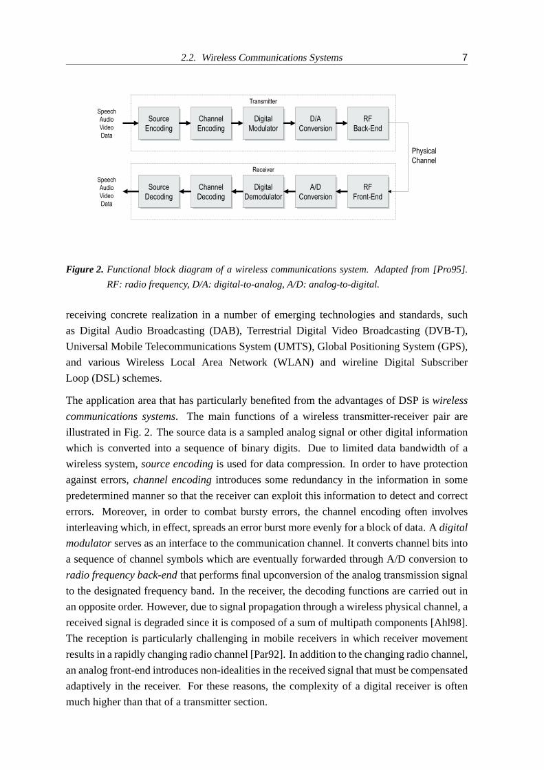
Figure 2. Functional block diagram of a wireless communications system. Adapted from [Pro95].
RF: radio frequency, D/A: digital-to-analog, A/D: analog-to-digital.
receiving concrete realization in a number of emerging technologies and standards, such
as Digital Audio Broadcasting (DAB), Terrestrial Digital Video Broadcasting (DVB-T),
Universal Mobile Telecommunications System (UMTS), Global Positioning System (GPS),
and various Wireless Local Area Network (WLAN) and wireline Digital Subscriber
Loop (DSL) schemes.
The application area that has particularly benefited from the advantages of DSP is wireless
communications systems. The main functions of a wireless transmitter-receiver pair are
illustrated in Fig. 2. The source data is a sampled analog signal or other digital information
which is converted into a sequence of binary digits. Due to limited data bandwidth of a
wireless system, source encoding is used for data compression. In order to have protection
against errors, channel encoding introduces some redundancy in the information in some
predetermined manner so that the receiver can exploit this information to detect and correct
errors. Moreover, in order to combat bursty errors, the channel encoding often involves
interleaving which, in effect, spreads an error burst more evenly for a block of data. A digital
modulator serves as an interface to the communication channel. It converts channel bits into
a sequence of channel symbols which are eventually forwarded through A/D conversion to
radio frequency back-end that performs final upconversion of the analog transmission signal
to the designated frequency band. In the receiver, the decoding functions are carried out in
an opposite order. However, due to signal propagation through a wireless physical channel, a
received signal is degraded since it is composed of a sum of multipath components [Ahl98].
The reception is particularly challenging in mobile receivers in which receiver movement
results in a rapidly changing radio channel [Par92]. In addition to the changing radio channel,
an analog front-end introduces non-idealities in the received signal that must be compensated
adaptively in the receiver. For these reasons, the complexity of a digital receiver is often
much higher than that of a transmitter section.
8 2. Wireless Communications System Design
Gain
Control
Rake
Finger
Bank
Wideband
Power
Multipath
Combiner
Symbol
Scaling
SIR
Estimation
FED
Code
Generators
AFC
AGC
Complex
Channel Estimation
Narrowband
Power
Mux
Multipath Delay
Estimation
Pulse Shaping
FilteringFrequency
Control
Channel
Bits
SIR
Multipath
Profile
From A/D
Converter
Channel
Bits
Code Generators
Special
Chip Sequences
Quadrature
ModulationSpreading/Scrambling
MuxSymbol
Mapping
Pulse Shaping
FilteringTo D/A
Converter
Transmitter
Receiver
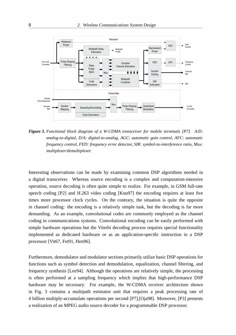
Figure 3. Functional block diagram of a W-CDMA transceiver for mobile terminals [P7]. A/D:
analog-to-digital, D/A: digital-to-analog, AGC: automatic gain control, AFC: automatic
frequency control, FED: frequency error detector, SIR: symbol-to-interference ratio, Mux:
multiplexer/demultiplexer.
Interesting observations can be made by examining common DSP algorithms needed in
a digital transceiver. Whereas source encoding is a complex and computation-intensive
operation, source decoding is often quite simple to realize. For example, in GSM full-rate
speech coding [P2] and H.263 video coding [Knu97] the encoding requires at least five
times more processor clock cycles. On the contrary, the situation is quite the opposite
in channel coding: the encoding is a relatively simple task, but the decoding is far more
demanding. As an example, convolutional codes are commonly employed as the channel
coding in communications systems. Convolutional encoding can be easily performed with
simple hardware operations but the Viterbi decoding process requires special functionality
implemented as dedicated hardware or as an application-specific instruction in a DSP
processor [Vit67, Fet91, Hen96].
Furthermore, demodulator and modulator sections primarily utilize basic DSP operations for
functions such as symbol detection and demodulation, equalization, channel filtering, and
frequency synthesis [Lee94]. Although the operations are relatively simple, the processing
is often performed at a sampling frequency which implies that high-performance DSP
hardware may be necessary. For example, the W-CDMA receiver architecture shown
in Fig. 3 contains a multipath estimator unit that requires a peak processing rate of
4 billion multiply-accumulate operations per second [P7],[Oja98]. Moreover, [P3] presents
a realization of an MPEG audio source decoder for a programmable DSP processor.
2.3. Wireless System Design 9
2.3 Wireless System Design
Wireless communications systems, such as mobile phones and other wireless terminals, are
ultra high-volume consumer market products which are implemented as highly integrated
systems. These systems are portable, battery-powered embedded systems that are strongly
influenced by constraints on system cost, size, and power consumption [Teu98]. Moreover,
the development of such an embedded system should be favorably characterized by attibutes
such as fast design turn-around, design flexibility, and reliability.
Currently, system implementations are based on advanced communications platforms
which employ the latest semiconductor technologies and components integrated into a
system-level application-specific integrated circuit that is more commonly referred to as a
system-on-a-chip (SOC) [Cha99]. This kind of chip is a high-performance multiprocessor
system which incorporates various types of hardware cores: programmable processors,
application-specific integrated circuit (ASIC) blocks, on-chip memories, peripherals, analog
components, and various interface circuits.
2.3.1 System Design Flow
Embedded system design for wireless terminals is strongly influenced by system-level
considerations. At system level, primary influences include wireless operating environment,
receiver mobility, applications, and constraints on system cost, size, power consumption,
flexibility, and design time [Knu99]. In [Cam96], an embedded system is defined as a
real-time system performing a dedicated, fixed function or functions where the correctness
of the design is crucial. Specification and design of these systems consists of describing a
system’s desired functionality and mapping that functionality for implementation by a set
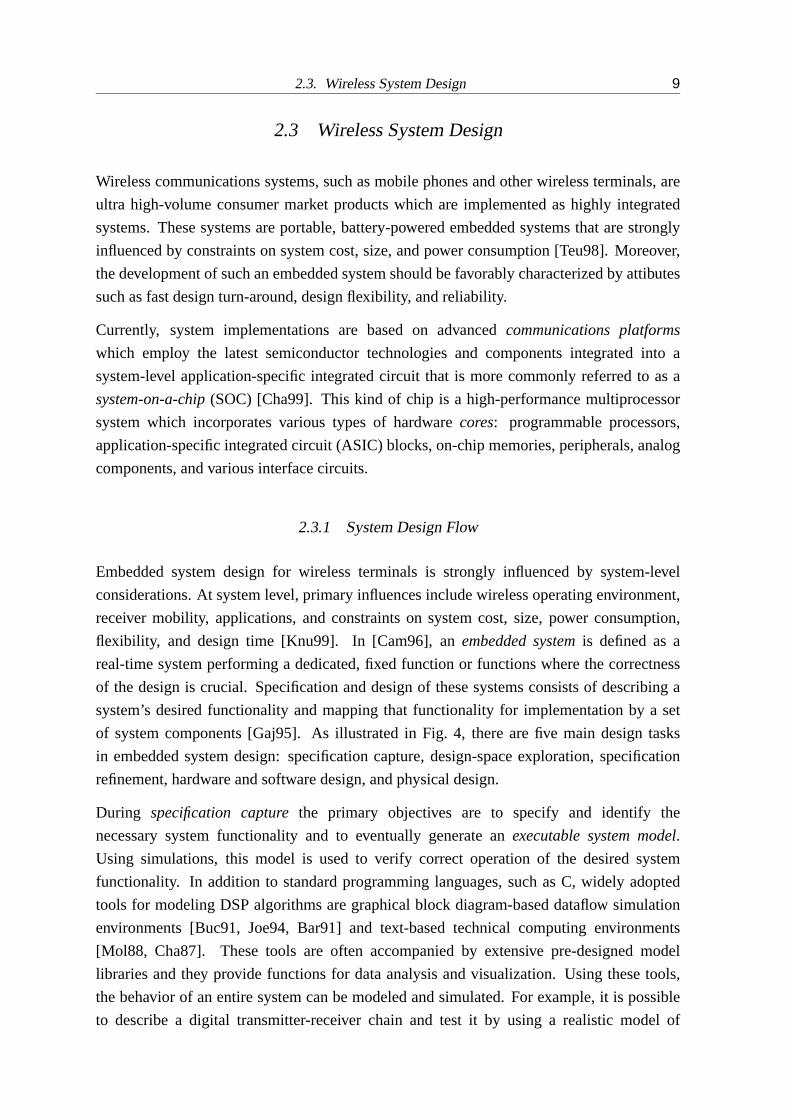
of system components [Gaj95]. As illustrated in Fig. 4, there are five main design tasks
in embedded system design: specification capture, design-space exploration, specification
refinement, hardware and software design, and physical design.
During specification capture the primary objectives are to specify and identify the
necessary system functionality and to eventually generate an executable system model.
Using simulations, this model is used to verify correct operation of the desired system
functionality. In addition to standard programming languages, such as C, widely adopted
tools for modeling DSP algorithms are graphical block diagram-based dataflow simulation
environments [Buc91, Joe94, Bar91] and text-based technical computing environments
[Mol88, Cha87]. These tools are often accompanied by extensive pre-designed model
libraries and they provide functions for data analysis and visualization. Using these tools,
the behavior of an entire system can be modeled and simulated. For example, it is possible
to describe a digital transmitter-receiver chain and test it by using a realistic model of
10 2. Wireless Communications System Design
Specification Refinement
Hardware and Software Design
Physical Design
Design-Space Exploration
Specification Capture
Functional Specification
System-Level Description
RT-Level Description
Physical Description(to manufacturing and testing)
Model Creation Description Generation
Executable Model Functional Simulation
Transformation Allocation Partitioning Estimation
Memories Interfaces Arbitration Generation
MCU DSP ASIC Memory Peripherals
C/C++ Code RTL Code Memory-Mapped Address Space
Code Compilation/Assembly Coding Placement,Routing,Timing
Validation-
Verification
Simulation and
Cosimulation
Software Synthesis High-Level Synthesis Logic Synthesis
Task:
Product:
Figure 4. System-level design process of embedded systems. Adapted from [Gaj95].
the radio transmission channel. In addition, most dataflow simulation environments allow
heterogenous simulations with implementation-level hardware descriptions [P6].
In design-space exploration the modeled functionality is transformed and partitioned into a
number of target architectures, or platforms, that contain different sets of allocated system
components, such as programmable processors, ASICs, and memory. Using estimation,
the objective is to find a feasible architecture that meets the criteria for real-time operation,
performance, cost, and power consumption. A software function is estimated in terms of
program code size and worst-case run-time for a function, i.e. the number of processor
clock cycles. For a given processor, software power consumption can be approximated if a
reliable metric, such as mW/MHz, is provided for active and idle modes by the processor
vendor. In contrast, an ASIC-based function is estimated with respect to the number of
logic gates or transistors, die area, and power consumption. For CMOS technologies, power
consumption of digital hardware circuits depends primarily on the internal activity factor,
operating voltage, and operating frequency [Cha95]. However, power consumption in ASIC
cores is highly dependent on the internal fine-structure and thus it is relatively hard to
estimate. In practice, comparing an implementation of a function realized as an ASIC core
and a program executed on a programmable processor can be very difficult and laborious if
very accurate estimates are needed.

2.3. Wireless System Design 11
After design-space exploration a suitable target architecture has been formed. In
specification refinement a more detailed description of the system architecture is created
by specifying bus structures and arbitration, system timing, and interfaces between cores
and off-chip elements. This system-level description contains some implementation details,
but the functionality is mainly composed of behavioral models. In hardware/software
co-simulation, verification is carried out by combining hardware description language
(HDL) and instruction-set simulators to permit co-simulation of a complete system. Due
to the use of HDL simulators, simulation speed can become a bottleneck in the verification
of complex systems. Recently, simulation environments employing C/C++ language-based
models have been reported to accelerate co-simulation by a factor of three [Sem00]. In
addition to co-simulation, C/C++ models may soon provide a path to implementation with
hardware synthesis [Gho99, DM99].
Hardware and software design is a concurrent task that involves description of both
hardware and software components by separate design teams. This task is carried out as
hardware/software co-design where the correct interaction of implementations is verified
using co-simulation. For software, target components are programmable processors, such
as embedded RISC and DSP processors [Hen90, Lap96]. Software is tested, profiled, and
debugged by executing program code in processor models that emulate the operation of a
real processor. With respect to the simulation accuracy and speed, various processor models
can be utilized [Cha96]. Currently, typical processor models are instruction-set simulators
that allow cycle-accurate simulation of an entire processor architecture at a speed of 0.1-0.3
million instruction cycles per second [P2]. Furthermore, when a physical prototype of a
processor is available, it is possible to perform software emulation in real-time using an
evaluation board, such as the one reported in [P5]. Hardware design is based on modeling the
desired functions at register-transfer level (RTL) by using standard languages, such as VHDL
and Verilog [IEE87, Tho91]. With the aid of logic synthesis tools, these RTL descriptions
are transformed into gate-level netlists that essentially capture the fine-structure of an ASIC.
As opposed to ASIC and programmable processors, an increasingly popular approach
to improve flexibility and performance is application-specific instruction-set processors
(ASIPs). These tailored processors execute specialized functions with a customized set of
resources and relatively small program kernels [Nur94, Lie94, Goo95].
In physical design a transistor-level chip layout is generated. System components are placed
and wired using automatic tools according to a chip floorplan. In order to create the
physical layout of a synthesized ASIC core, placement and routing of standard library cells
is required [Smi97]. For programmable processors, executable program code is compiled
from high-level language and assembly source codes.
12 2. Wireless Communications System Design
EBM
EMCInterrupt
Controller ARM
RISC MCU
OAK
DSP
RAMCacheDual
Port
RAM
RAMRAM
Ctrl
DMA
Controller
USB IF UARTSmartcard
IF
Parallel
Port
Bus
Bridge
Peripheral
Bus IF
G726
ADPCM
Echo Canceller
DECT
Burst Mode
Control
Shared
RAM
ROM RAM
Codec
Radio
IF
ADC DAC
DECT Communications Platform
FPGA
FPGA RF Section
MCU
DRAM
Flash
EEPROM
SRAM
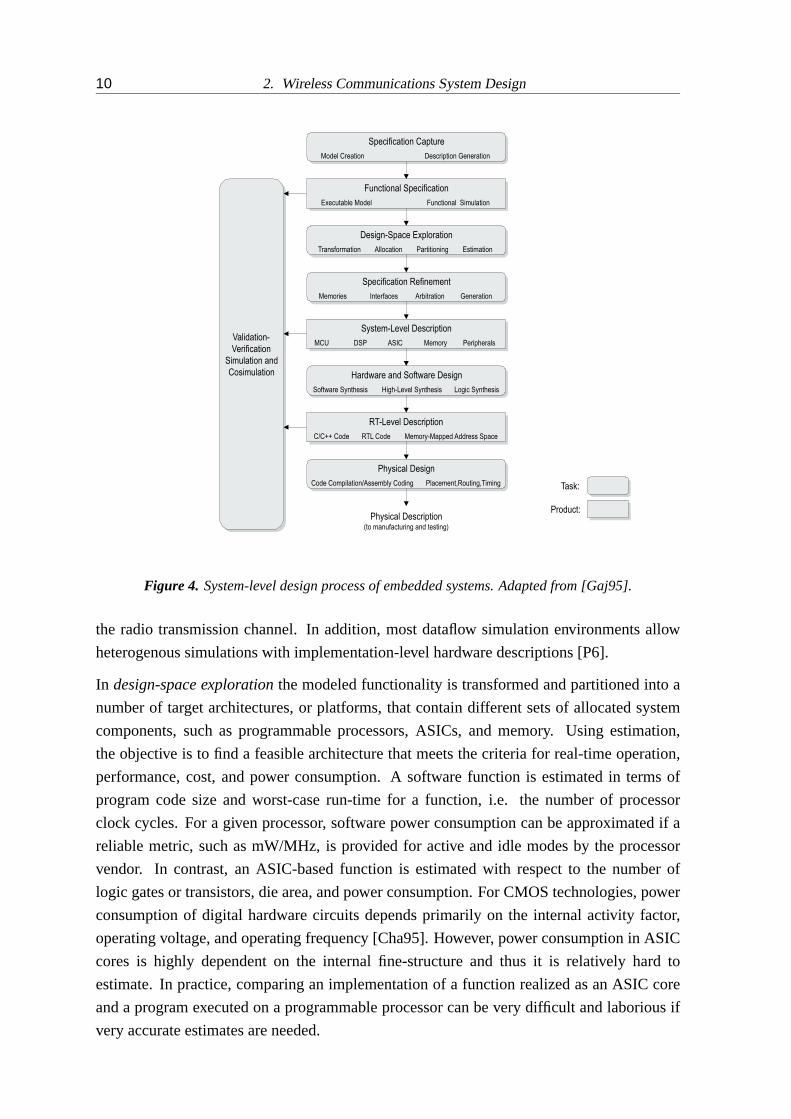
Figure 5. Example of an integrated DECT communications platform. System is based on three
programmable processors: an embedded RISC processor, a DSP processor and an ASIP
for ADPCM vocoding and echo cancellation [Cha99]. EMC: external memory controller,
EBM: external bus master, IF: interface.
2.3.2 Processor Core-Based Design
Earlier single-chip systems have preferred implementations based mainly on ASIC cores
which, due to tailored arhitecture, have a potential for smaller power consumption,
smaller die area, and especially better performance. However, the rapid advances in
CMOS technologies have enabled development of large, complex systems on a chip by
exploiting reusable programmable processor cores which are now characterized by low
power consumption due to voltage scaling, high-performance hardware circuitry, and a
diminishing die area when compared to the size of the on-chip memories. For a system
developer, these pre-designed, pre-verified cores provide an attractive means for importing
advanced technology into a system. Most importantly, processor core use shortens the time
to market for new system designs and allows straightforward product differentiation through
programmability. As an example, Fig. 5 depicts an integration platform for Digital Enhanced
Cordless Telecommunications (DECT) applications [Cha99, ETS92]. The system is based
on three buses and contains a total of three programmable processors, various memory
blocks, and a variety of digital interfaces and data converters.
Typically embedded processor cores are delivered either in a soft or hard form. Soft cores
are processor cores delivered as synthesizable RTL HDL code and optimized synthesis
scripts and thus they can quickly be retargeted to a new semiconductor technology provided
that a standard-cell library is available. Hard cores, in turn, are designed for a certain

2.3. Wireless System Design 13
semiconductor technology and delivered as fixed transistor-level layouts, typically in the
GDSII format. As opposed to soft cores, hard cores generally perform better in terms of
die area and power consumption. However, when core portability is of primary concern, a
soft core should be preferred. Another issue is the business model used by the processor
core vendor. A licensable core is handed over to a system developer as a complete
design [Lap96]. Thus the core licensee may have the potential to change the design
if the core is soft. The most widely-used licensable processor cores are ARM, MIPS,
PineDSPCore, and OakDSPCore [ARM95, Sch98, Be’93, Ova94]. Hard cores are often
foundry-captive cores because the core vendor has considerable intellectual property in an
optimized transistor-level design. Therefore, in a chip floorplan, a foundry-captive core is
introduced as a black box. For example, designs incorporating a DSP processor from the
TMS320C54x family are explicitly manufactured by the core vendor [Lee97, Tex95].
According to system partitioning, different software functions should be mapped to
appropriate processor types when possible. A coarse mapping to microcontroller units
(MCU) and digital signal processing (DSP) processors can be performed by examining
the properties of the system tasks. Whereas control-dominated software functions are
better-suited to MCUs, DSP processors are an ideal target for most computation-intensive
signal processing tasks.
The processing capacity of an embedded processor is specified by its internal clock frequency
that effectively specifies the number of clock cycles per second that can be utilized for
program execution. For functions under strict real-time constraints, the processor load should
be profiled to guarantee correct behavior during active operation. Generally, this requires
estimation of the worst-case run-times for real-time system tasks. The estimation should also
take into account the overhead resulting, for example, from interrupt processing, bus sharing,
and memory access latencies. In this context, a metric called cycle budget is used to refer
to the maximum number of clock cycles per second for a given processor. Often the term
million instructions per second (MIPS) is used as a synonym for cycle budget. This loose
metric is generally computed by multiplying the processor clock frequency by its instruction
issue width or the number of multiply-accumulate units. Consequently a given MIPS value
assumes a single-cycle fully parallel execution of instructions at all times thus the value
generally specifies a theoretical peak performance. Therefore, more reliable metrics for
processor performance are application benchmarks, such as general computing applications
and certain algorithm kernels.
To conclude, the increasing demand for implementation flexibility implies that functionality
should be pushed towards software as much as possible while still fulfilling a given set of
constraints, especially for performance and power consumption.

3. PROGRAMMABLE PROCESSOR ARCHITECTURES
This chapter covers various classifications which can be used to differentiate programmable
processors. The chapter presents a comprehensive description of the primary characteristics
found in modern instruction-set architectures and discusses a number of techniques which
are applied to programmable processors to enhance their instruction throughput and
computational performance.
3.1 Instruction-Set Architectures
An instruction-set architecture (ISA) can be viewed as a set of resources provided by a
processor architecture that are available to the programmer or a compiler designer [Heu97].
These resources are defined in terms of memory organization, size and type of register sets,
and the way instructions access their operands both from registers and memory.
In the early phases of processor evolution, designers began to develop instruction sets so that
the processor directly supported many complex constructs found in high-level languages.
This approach lead to very complex instruction sets. Often execution of an instruction was
a long sequence of operations carried out sequentially in a processor that had very restricted
hardware resources. An execution sequence was essentially stored as a set of microcodes
that correspond to low-level control programs. In retrospect today these types of processors
are referred to as complex instruction-set computer (CISC) machines. CISC-type processors
are typically characterized by long and variable-length instruction words, a wide range of
addressing modes, one arithmetic-logic unit, and a single main memory that is used to store
both program code and data.
Due to the very complex control flow, the performance of CISC machines was very
difficult to improve. It was shown that by decomposing one complex instruction into a
number of simple instructions and by allowing parallel execution of these instructions, the
performance could be improved significantly. Moreover, data memory accesses use distinct
register loads and stores, and data operations have only register operands. These are the
fundamental concepts of the reduced instruction-set computer (RISC) design philosophy.
Other key characteristics of a RISC machine are: fixed-length 32-bit instruction word, large
general-purpose register files, simplified addressing modes, pipelining, and program code
generation with sophisticated software compilers [Bet97, Heu97].

16 3. Programmable Processor Architectures
a) b) c)
Program
Memory
Data
Memory
Processor
Program and Data
Memory
Processor
Program
Memory
Data
Memory
Processor
Data
Memory
Figure 6. Processor memory architectures: a) von Neumann architecture, b) basic Harvard
architecture, and c) modified Harvard architecture. [Lee88].
3.1.1 Memory Organization
All programmable processor architectures require memory for two main purposes: to store
data values and instruction words constituting executable programs. In this context, different
memory organizations are categorized into three types of architectures: von Neumann, basic
Harvard, and modified Harvard.
The configuration of these memory architectures is illustrated in Fig. 6. In the past, a single
memory was employed for both data and programs. This architecture is known as von
Neumann architecture. However, the memory architecture poses a bottleneck in memory
accesses since an instruction fetch requires a separate access and thus always blocks a
potential data memory access. Consequently, the evident bottleneck was circumvented with
Harvard architecture that holds separate memories for both program and data. In the basic
Harvard architecture, program and data memory accesses can be made simultaneously and
thus program execution does not hinder data memory transfers. This architecture is currently
found in virtually all high-performance microprocessors in the form of separate cache
memories for instructions and data [Hen90]. However, the modified Harvard architecture is
the dominant memory architecture employed in DSP processors. The memory architecture
incorporates two data memories to permit simultaneous fetch of two operands.
In addition, a number of variations have been reported in DSP processor systems. For
example, using a special DSP instruction in a single instruction repeat loop, a third
operand can be fetched from the program memory, thus effectively fetching a total of
three input operands at a time [Tex97a]. Memory architectures supporting four parallel
data memory transfers have been reported in [Suc98]. Moreover, some recent DSP
processor architectures incorporate a supplementary program memory which contains wide
microcodes to realize highly parallel instructions without enlarging the width of the native
instruction word [Kie98, Suc98].
3.1. Instruction-Set Architectures 17
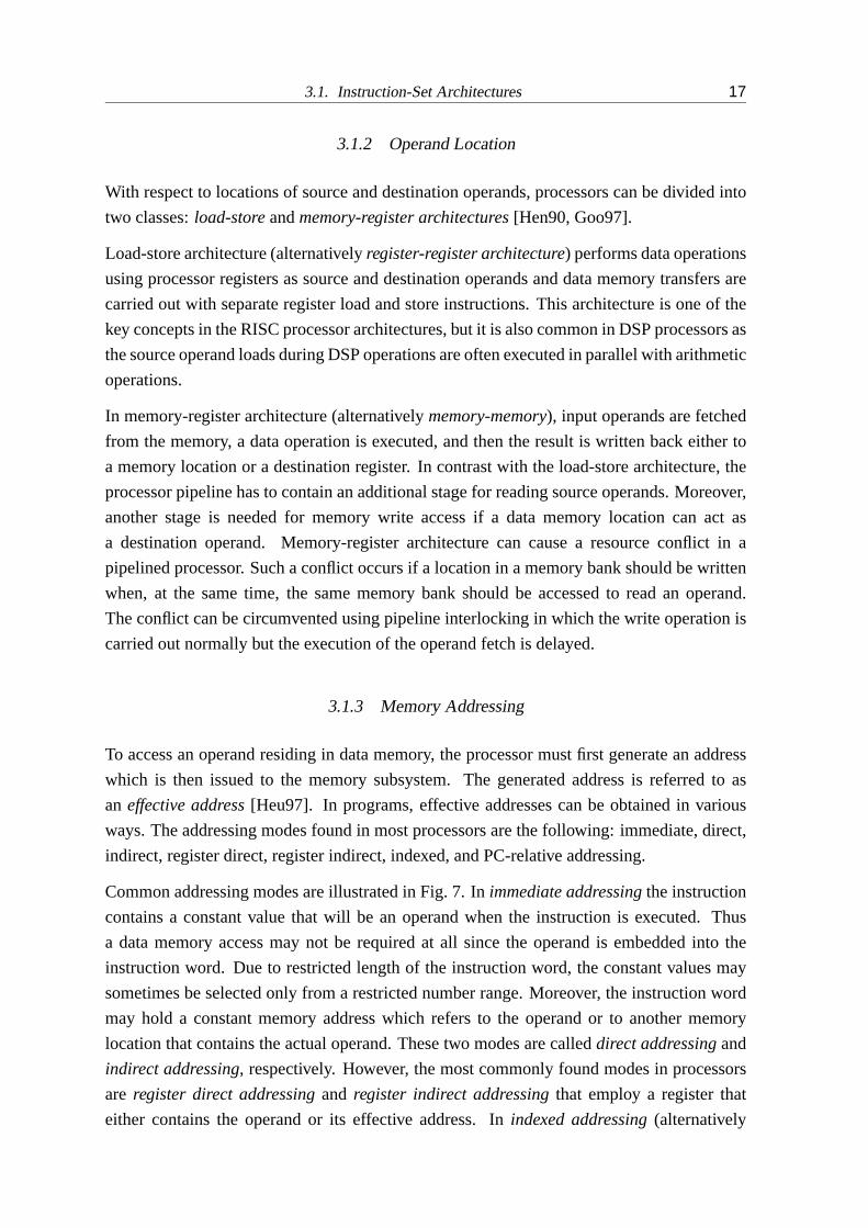
3.1.2 Operand Location
With respect to locations of source and destination operands, processors can be divided into
two classes: load-store and memory-register architectures [Hen90, Goo97].
Load-store architecture (alternatively register-register architecture) performs data operations
using processor registers as source and destination operands and data memory transfers are
carried out with separate register load and store instructions. This architecture is one of the
key concepts in the RISC processor architectures, but it is also common in DSP processors as
the source operand loads during DSP operations are often executed in parallel with arithmetic
operations.
In memory-register architecture (alternatively memory-memory), input operands are fetched
from the memory, a data operation is executed, and then the result is written back either to
a memory location or a destination register. In contrast with the load-store architecture, the
processor pipeline has to contain an additional stage for reading source operands. Moreover,
another stage is needed for memory write access if a data memory location can act as
a destination operand. Memory-register architecture can cause a resource conflict in a
pipelined processor. Such a conflict occurs if a location in a memory bank should be written
when, at the same time, the same memory bank should be accessed to read an operand.
The conflict can be circumvented using pipeline interlocking in which the write operation is
carried out normally but the execution of the operand fetch is delayed.
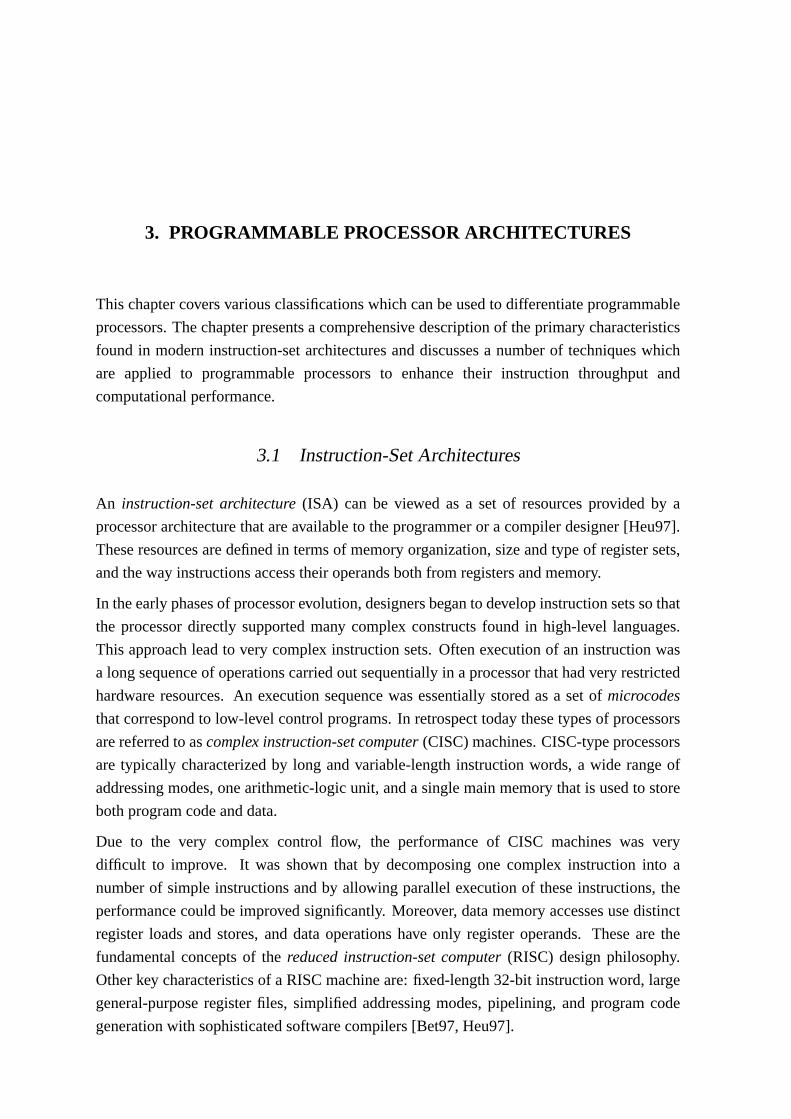
3.1.3 Memory Addressing
To access an operand residing in data memory, the processor must first generate an address
which is then issued to the memory subsystem. The generated address is referred to as
an effective address [Heu97]. In programs, effective addresses can be obtained in various
ways. The addressing modes found in most processors are the following: immediate, direct,
indirect, register direct, register indirect, indexed, and PC-relative addressing.
Common addressing modes are illustrated in Fig. 7. In immediate addressing the instruction
contains a constant value that will be an operand when the instruction is executed. Thus
a data memory access may not be required at all since the operand is embedded into the
instruction word. Due to restricted length of the instruction word, the constant values may
sometimes be selected only from a restricted number range. Moreover, the instruction word
may hold a constant memory address which refers to the operand or to another memory
location that contains the actual operand. These two modes are called direct addressing and
indirect addressing, respectively. However, the most commonly found modes in processors
are register direct addressing and register indirect addressing that employ a register that
either contains the operand or its effective address. In indexed addressing (alternatively

18 3. Programmable Processor Architectures
Operand
Op Constant Address
Op Constant Value
Op Reg
Operand
Operand
Operand
a)
b)
c)
f)
e)
Operand
d)g)
Operand
Memory
Operand
Operand Address
Memory
Register
Register
Register
Program Counter
Memory
Memory
Memory
Op Constant Address
Op ConstantReg
Op ConstantReg
Op Constant
Figure 7. Common addressing modes: a) immediate, b) direct, c) indirect, d) register direct, e)
register indirect, f) indexed, and g) PC-relative addressing. A grey block represents an
instruction word. [Heu97].
offset or displacement addressing) the effective address is formed by adding a small constant
to the value stored in a register. In PC-relative addressing the explicit register utilized in
the address calculation is the program counter (PC). PC-relative addressing is particularly
well-suited for relocatable program modules in which the program and data sections can be
placed in any memory location and accessed with valid effective addresses.
3.1.4 Number Systems
In digital computers a numeric value is represented with a data word composed of a specified
number of binary digits, or bits. Therefore, due to the finite word length all computer
arithmetics are implemented as operations with a finite accuracy. Generally, the number
systems found in programmable procesors can be divided into two classes: fixed-point and
floating-point numbers [Hwa79].
In fixed-point numbers the binary point (alternatively radix point) is in a specific position of
a data word. Although there are several ways to represent signed binary numbers, only the
two’s complement format is considered in this context. This format is clearly the dominant
one of the fixed-point number representations because the arithmetic operations are simple
to realize in hardware. Two commonly used numbers are integer and fractional numbers.
The difference between these two is that whereas integer numbers have the binary point
at the extreme right, fractional numbers normally have the binary point right of the most
3.2. Enhancing Processor Performance 19
significant bit, i.e. the sign bit. Assuming two’s complement format and a data word x
of length N, a fractional number is bounded to −1≤ x < 1 and a signed integer number to
−2N−1≤ x < 2N−1. In the technical literature fractional numbers are often referred to as Q15
and Q31 for 16-bit and 32-bit data words, respectively. An interesting observation from the
hardware design point of view is that in practice the standard integer and fractional arithmetic
operations can be implemented with the same hardware units with only minor adjustments.
Floating-point numbers are composed of a mantissa (alternatively significand) and an
exponent in a single data word [Lap96]. The exponent is always an integer that defines
the conceptual location of the binary point with respect to the value stored in the mantissa.
The mantissa contains a signed value which is scaled by a factor specified by the
exponent. In this context, an exponent base of 2 is assumed. Thus, a numerical value
x of a floating-point number with a signed mantissa m and exponent e is computed with
the expression x = m×2e. In 1985, a common framework for binary floating-point
arithmetic was specified in ANSI/IEEE standard 754 [ANS85]. The standard not only
specifies floating-point number formats for 32-bit and 64-bit data words but also defines
a comprehensive set of rules for how operations, rounding, and exception conditions are
to be performed. The hardware required for native floating-point arithmetic is extensive.
Moreover, a floating-point format typically has a data word that has at least 32 bits, which
consequently results in larger data memory consumption. For these reasons the most
low-cost DSP processors do not implement the 754 standard for the sake of reduced hardware
cost. Instead, most fixed-point DSP processors provide support for proprietary floating-point
arithmetic by incorporating additional hardware and special instructions for normalization
and derive-exponent operations [Lap96].
Block floating-point numbers are an important alternative for a fixed-point processor in
gaining some of the increased dynamic range without the hardware overhead associated
with floating-point arithmetic [Wil63]. In this scheme a single exponent is utilized for
an array of fixed-point values. This format lends itself particularly well to block-based
signal processing that is found in applications such as digital filtering [Sri88, Kal96] and
fast transforms [Eri92, Bid95].
3.2 Enhancing Processor Performance
3.2.1 Pipelining
In the context of processor operation, pipelining is a hardware implementation technique
whereby execution of multiple instructions overlaps in time. The steps, or operations,
required to execute an instruction are carried out in discrete steps in the processor pipeline.
These steps are referred to as pipeline stages. Operations during the pipeline stages are
20 3. Programmable Processor Architectures
separated using pipeline registers. An instruction cycle is defined as the period of time that
is used to shift an instruction to the next pipeline stage. This can be one or more processor
clock cycles.
Pipelining significantly improves instruction throughput since ideally a program is executed
in such a manner that one instruction is completed on every clock cycle. Thus increased
instruction throughput translates into higher performance. This basic form of pipelined
processor which sequentially issues one instruction per clock cycle is called a scalar
processor (alternatively single-issue processor). To the programmer the processor pipeline
can be either visible or hidden. A visible pipeline relies on the programmer’s knowledge
that, for certain instructions, the result may not yet be available for the next instruction. In a
hidden pipeline, the processor itself takes care of these situations.
However, due to data and control dependencies between instructions and limited processor
resources, the performance is often slightly degraded. Still, with careful design of the
processor ISA the instruction throughput can be made very close to the ideal operation,
i.e. a single clock cycle per instruction. In order to avoid various pipeline hazards, the
pipelined operation often requires sophisticated hardware structures for pipeline interlocking
and forwarding (alternatively bypassing) of the computed results. Detailed treatment of
this broad subject is beyond the scope of this thesis, but excellent coverage can be found
in [Hen90].
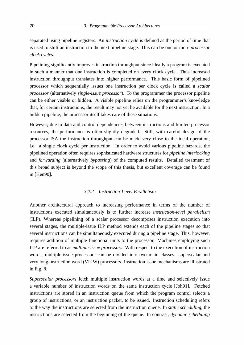
3.2.2 Instruction-Level Parallelism
Another architectural approach to increasing performance in terms of the number of
instructions executed simultaneously is to further increase instruction-level parallelism
(ILP). Whereas pipelining of a scalar processor decomposes instruction execution into
several stages, the multiple-issue ILP method extends each of the pipeline stages so that
several instructions can be simultaneously executed during a pipeline stage. This, however,
requires addition of multiple functional units to the processor. Machines employing such
ILP are referred to as multiple-issue processors. With respect to the execution of instruction
words, multiple-issue processors can be divided into two main classes: superscalar and
very long instruction word (VLIW) processors. Instruction issue mechanisms are illustrated
in Fig. 8.
Superscalar processors fetch multiple instruction words at a time and selectively issue
a variable number of instruction words on the same instruction cycle [Joh91]. Fetched
instructions are stored in an instruction queue from which the program control selects a
group of instructions, or an instruction packet, to be issued. Instruction scheduling refers
to the way the instructions are selected from the instruction queue. In static scheduling, the
instructions are selected from the beginning of the queue. In contrast, dynamic scheduling

3.2. Enhancing Processor Performance 21
...
...
...
...
...
...
...
d)
c)
b)
a)
Clock
Cycle
N N N+1 N+1
N N+1 N+2 N+3 N+4
N N N+1 N+1
N+5 N+6 N+7
N
N+1
N+2
N+3
N+4
N+5
N+6
N+7
N+8
N+9
N+10
N+11
N+12
N+13
N+14
N+15
N+16
N+17
N+18 N+19
N+20
N+21
N+22
N N+4 N+7N+1 N+2 N+3 N+5 N+6
3 4 5 61 2 7 8
Figure 8. Illustration of instruction issue mechanisms in processors: a) scalar non-pipelined, b)
scalar pipelined, c) superscalar pipelined, and d) VLIW pipelined. White blocks represent
unused issue slots or no-operation fields for superscalar and VLIW processors, respectively.
allows the instructions to be issued out of order. Thus dynamic scheduling is more commonly
called out-of-order instruction execution. A superscalar processor always contains special
hardware that selects which of the currently fetched instructions can be grouped together and
then issued. The main drawback of superscalar operation is that this hardware can be very
expensive in terms of silicon area. The superscalar approach is currently employed mostly
in general-purpose processors. Classical examples of superscalar architectures include
high-performance RISC microprocessors, such as PowerPC [Ken97], Alpha [Kes98], HP-PA
[Kum97], and Sparc [Gre95] families, and the well-known CISC microprocessors based on
the x86 ISA [Alp93, Gol99].
In contrast to the superscalar approach, VLIW processors employ significantly wider
instruction words to enforce static instruction issue and scheduling. In effect, a wide
instruction word is a compiler-scheduled instruction packet that has instruction fields for all
the functional units in the processor. The instruction field either specifies a useful operation
or the field contains a no-operation. The main advantage of the VLIW approach is reduced
implementation cost. As opposed to superscalar processors, program control hardware can
be made minimal because complicated instruction grouping and dispatch mechanisms are not
needed. An obvious drawback of the VLIW approach is the lengthy instruction word which,
in turn, results in a large program code size. However, this drawback has been circumvented
to some extent by using compressed VLIW instructions. Compression translates a normal
22 3. Programmable Processor Architectures
VLIW instruction word into a variable-length word by encoding the no-operation fields in
some predetermined manner. In the program execution a compressed instruction word is
eventually decompressed back to the original VLIW format. DSP processors employing
instruction compression have recently been reported in [Ses98, Rat98]. An alternative term
for compressed VLIW instruction is variable-length execution set (VLES) [Roz99].
Interestingly, the high-performace x86 microprocessors employ a complicated decoding unit
to permit multiple-issue for CISC instructions [Che98]. The decoding unit translates x86
instructions into several RISC-style primitive operations and issues them to the functional
units. Recently, a novel approach to carry out this translation in software in combination
with an advanced low-power VLIW architecture has been reported in [Kla00].
3.2.3 Data-Level Parallelism
In contrast to pipelining and multiple-issue techniques, data-level parallelism (DLP) can
be employed to leverage the amount of work performed by an individual instruction. This
approach is generally implemented in the form of single instruction stream, multiple data
stream (SIMD) instructions. The basic idea is to simultaneously perform an arithmetic
operation on a small array of data values. The wide acceptance of this approach is due
to the observation that the data values found in multimedia applications can be represented
with much less precision than the native data word width. For example, commonly utilized
data types in digital audio and video processing are 16 and 8 bits, respectively [Kur98].
Generally SIMD instructions can be realized either by utilizing the existing arithmetic
units at subword precision or by including several duplicates of the arithmetic units. The
former alternative is especially well suited to general-purpose microprocessors that employ
a wide data word, such as 64 bits [Lee95]. A wide data word can be packed with several
lower precision data values and a wide arithmetic unit can be divided or split into smaller
subunits that carry out several operations at the same time. For example, a 64-bit ALU
can easily be implemented so that it can also perform either two 32-bit, four 16-bit, or
eight 8-bit operations. Additionally, SIMD instructions often incorporate extra functionality
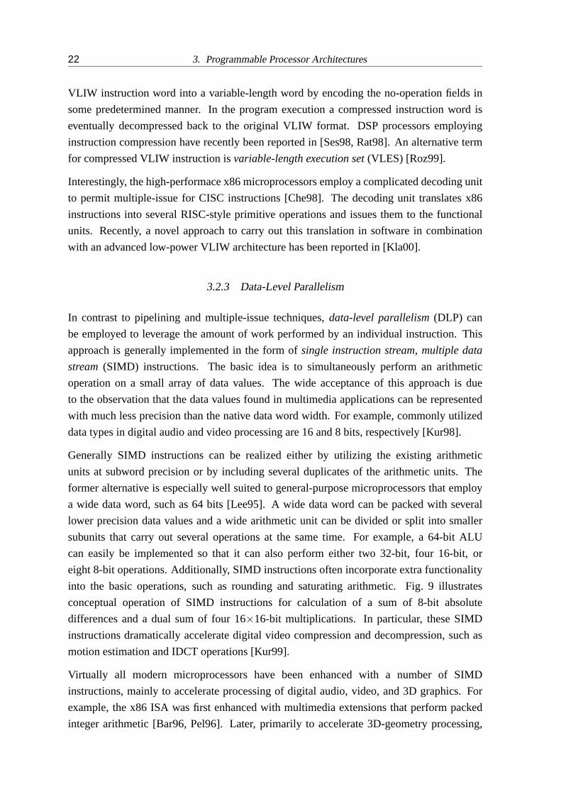
into the basic operations, such as rounding and saturating arithmetic. Fig. 9 illustrates
conceptual operation of SIMD instructions for calculation of a sum of 8-bit absolute
differences and a dual sum of four 16×16-bit multiplications. In particular, these SIMD
instructions dramatically accelerate digital video compression and decompression, such as
motion estimation and IDCT operations [Kur99].
Virtually all modern microprocessors have been enhanced with a number of SIMD
instructions, mainly to accelerate processing of digital audio, video, and 3D graphics. For
example, the x86 ISA was first enhanced with multimedia extensions that perform packed
integer arithmetic [Bar96, Pel96]. Later, primarily to accelerate 3D-geometry processing,
3.2. Enhancing Processor Performance 23
Op1 Op3 Op5 Op7 Op9 Op11 Op13 Op15
Op2 Op4 Op6 Op8 Op10 Op12 Op14 Op16
8 x 8-bits
a) b)
64-bits
Reg A
Reg B
Reg C
Op1 Op3 Op5 Op7
Op2 Op4 Op6 Op8
4 x 16-bits
++
2 x 32-bits
+ +
- - - - - - - -
+
+
Sum
Abs Abs Abs Abs Abs Abs Abs Abs�
Acc1 Acc2
×� × ×�
Figure 9. Examples of special SIMD instructions realized using split arithmetic units at subword
precision: a) a sum of eight absolute differences [Tre96] and b) a dual sum of four
multiplication operations [Bar96]. Abs: absolute value operator.
SIMD-style instructions were added that allow two parallel single-precision floating-point
operations to be computed [Obe99]. SIMD enhancements for PowerPC, Sparc, and MIPS
RISC processors have been reported in [Ful98, Tre96, Kut99]. It should be noted that DSP
processors realize SIMD instructions often by duplication of arithmetic units because the
length of the native data word is typically only 16 bits.
3.2.4 Task-Level Parallelism
Traditional uniprocessor computer systems are constructed around a single main central
processing unit (CPU). With the aid of an operating system kernel, a processor runs multiple
program threads by switching execution between active and idle processes. Thus at any given
instant only one program thread is executed. In order to raise task-level parallelism (TLP) in
a computer system, two main alternatives have been proposed: simultaneous multithreading
(SMT) and chip-multiprocessors (CMP) [Tul95, Olu96].
SMT is primarily intended to enhance the performance of wide-issue superscalar processors.
Whereas control and data dependencies in a single-threaded processor typically restrict the
level of ILP extracted from a thread, a processor employing SMT is capable of filling
unused issue slots with instructions from the other program threads. CMPs, however,
use relatively simple single-threaded processor cores while executing multiple threads in
parallel across multiple on-chip processor cores. These multiprocessor computer systems
divide an application into multiple program threads, each of which is executed in a separate

24 3. Programmable Processor Architectures
DSP56600
DSP
RAM/ROM
Memories
RAM/ROM
Memories
M•CORE
RISC MCU
DSP
Debug
Baseband
SP
Audio
SPShared
Memory
Smart-
Card IF
External
Bus IF
Keypad
IF
MU
QSPI
MCU
Debug
UARTMisc.
Timers
Protocol
Timer
Figure 10. Block diagram of an integrated cellular baseband processor architecture. System
integrates a RISC microcontroller unit (MCU) and DSP processor which communicate
using a shared memory block and messaging unit (MU) [Gon99]. IF: interface, SP:
serial port, UART: universal asynchronous receiver/transmitter, QSPI: queued serial port
interface.
processor. Thus, approaching the same paradigm from a different perspective, both the
SMT and CMP systems employ a computer organization generally referred to as multiple
instruction stream, multiple data stream (MIMD) [Hwa85]. From a purely architectural
point of view, the SMT processor’s flexibility makes it an attractive choice. However, the
scheduling hardware to support the SMT is rather complicated and, even more importantly,
the impact on the processor implementation cost is significant. For these reasons, CMP is
much more promising because it can employ already existing processor cores in combination
with the increasing IC capacity [Ham97].
In the past multiprocessor systems have been utilized solely for supercomputing applications,
mainly due to the ultra-high implementation cost. Almost 30 years after the invention
of the microprocessor the advances in the IC technology permit integration of several
programmable processors and memory on a single silicon die [Bet97]. In the early 1990s
the first applications to adopt this approach were embedded DSP systems. For example,
multiprocessor platforms realizing video teleconferencing and a wireline modem have been
described in [Sch91, Gut92, Reg94]. However, the breakthrough of this technology to the
consumer market was not feasible until such platforms could be manufactured in high volume
at a reasonable cost. The first commercially successful designs exploiting the CMP approach
were digital cellular phones where two programmable processors, a microprocessor and a
DSP processor, were integrated on a single silicon die [Gat00, Bru98, Bog96]. Such a system
architecture is depicted in Fig. 10.

4. PROGRAMMABLE DSP PROCESSORS
Programmable DSP processors are streamlined microcomputers designed particularly for
real-time number crunching. In addition to the sophisticated techniques described in
the previous chapter, DSP processors embody advanced features that push the level of
parallelism even further. This is made possible by exploiting the inherent fine-grain
parallelism found in the fundamental algorithms, functions, behaviors, and data operations
in the field of digital signal processing. In this chapter a detailed overview of DSP processor
architectures is given. The chapter concentrates on the processor cores themselves, i.e.
peripherals are not considered in this context. Moreover, to make the scope of the chapter
slightly narrower, the investigation is limited to fixed-point DSP processor cores that do not
have native hardware support for floating-point arithmetic operations.
4.1 Historical Perspective
The first processors that were designed particularly for digital signal processing tasks
emerged in the early 1980’s [Lee90a]. It is arguable, however, which processor constitutes
the first DSP processor. The candidates are AMI S2811, AT&T Bell Laboratories DSP1, and
NEC µPD7720 [Nic78, Bod81, Nis81]. The instruction cycle times for the S2811, DSP1,
and µPD7720 processors were 300, 800, and 250 ns, respectively. All these processors
had a hardware multiplier and some internal memory, thus permitting development of
stand-alone embedded system implementations. Although the 12-bit S2811 was announced
in 1978, working devices were not available until late 1982 due to problems in fabrication
technology. In 1979, the 16/20-bit DSP1 processor became available, but it was only
employed for in-house designs at AT&T. The 16-bit µPD7720 was released in 1980 and
was one of the most heavily used devices among the early DSP processors. To summarize,
depending on how one prioritizes an announcement of a new processor, a functional chip,
and public commercial availability, the choice for the first DSP processor can be justified in
different ways.
Other noteworthy processors to follow were Texas Instruments TMS32010 [Mag82] and
Hitachi HSP HD6180 [Hag82], both released in 1982. The TMS32010 processor was the first
member of what was to become the most widely used family of DSP processors. The HSP

26 4. Programmable DSP Processors
was the first DSP processor fabricated in a CMOS technology and it also was the first to
support a floating-point number format with a 12-bit mantissa and 4-bit exponent.
Today, twenty years after the first successful architectures, programmable DSP processors
have evolved into highly specialized microcomputers which can efficiently perform massive
amounts of computing.
4.2 Fundamentals
The primary function provided by a DSP processor is its ability to provide execution
of a multiply-accumulate (MAC) operation in one instruction cycle. Fundamentally, the
MAC operation performs a multiplication of two source operands and adds this product to
the results that have been calculated earlier. From the program execution point of view,
the MAC operation can be decomposed into several parallel operations: multiplication of
two operands, accumulation (addition or subtraction) with previously calculated products,
fetching of the next two source operands, and post-modification of the data memory
addresses. Thus, the MAC operation exhibits a high level of inherent parallelism that is
exploited in pipelined DSP processors.
Another speciality found in fixed-point DSP processors are the measures which are utilized
to combat loss of precision in arithmetic operations constrained by fixed-point numbers with
a finite word length. When two fixed-point numbers are multiplied, the product with full
precision is equal to the sum of the number of bits in the operands [Lee88]. Therefore,
discarding any of these bits introduces error in the computation, i.e. loss of precision. For
this reason fixed-point DSP processors perform multiplications at full precision [Lap96].
In the MAC operation, intermediate results are stored in an accumulator which, in order to
prevent undesirable overflow situations, provides additional guard bits for preservation of the
accuracy. This permits an accumulator register with n guard bits to perform accumulation
of 2n values with the confidence that an overflow will not occur. Furthermore, accumulation
operation incorporates special saturation arithmetic which, in operation, forces the result
to the maximum positive or negative value in imminent overflow situations [Rab72]. At
some point it is necessary to reduce the precision of results, typically to fit into the native
data word. In truncation the least significant bits of the full-precision result are simply
discarded. In effect this rounds signed two’s complement numbers down towards minus
infinity. A truncated value is always smaller than or equal to the original and thus adds a
bias to truncated values [Cla76]. In order to avoid this bias, many DSP processors provide
advanced rounding schemes, such as round-to-nearest and convergent rounding [Lap96].
Furthermore, some algoritms require fixed-point multiplications and ALU operations to be
performed at a higher precision than that dictated by the native data word length. For this

4.2. Fundamentals 27
LDC #63,d0
LOOP d0,loop_end
XOR c,c,c ; LDX (i0)+1,a0 ; LDY (i2)+1,b0
loop_end: MAC a0,b0,c ; LDX (i0)+1,a0 ; LDY (i2)+1,b0
ADD c,p,c
Figure 11. Assembly source code which implements a 64-tap FIR filter. Each row corresponds to
an instruction word. LDC: load constant, XOR: logical exclusive-or, LOOP: initialize
hardware loop, NOP: no-operation, MAC: multiply-accumulate, LDX/LDY: load from X/Y
data memory [VS97].
reason it has become imperative that the datapath supports extended-precision operations,
such as a 32×32-bit multiplication, which results in a 64-bit full-precision result. In order to
support these operations, it is required that 16×16-bit multiplications can be computed for a
mixture of signed and unsigned operands, i.e. they can be in both signed two’s complement
and unsigned binary formats.
In DSP algorithms it is quite common that long sequences of similar operations are executed
frequently. These sequences are most conveniently programmed as a software loop that,
for a known number of iterations, requires both decrementing and testing of the loop count
and a conditional branch to the beginning of the loop. Obviously this adds very undesirable
overhead to the looping since on each iteration several instruction cycles are spent in the
manipulation of the loop count and the branching penalty resulting from the pipelining. For
these reasons DSP processors include special functionality in the form of zero-overhead
hardware looping. This hardware is an independent functional unit which, by decrementing
and testing a loop count register, can force a fetch from a loop start address when necessary.
The hardware looping unit operates in parallel with the normal program execution and thus
the looping operation adds no overhead once a hardware loop has been initialized.
The peak achievable ILP can be extremely high in DSP processors, which is illustrated
with a piece of assembly source code shown in Fig. 11. In the example a hardware loop
is initialized and a stream of consecutive MAC operations is executed. The loop body is
composed of a single instruction word which contains a MAC operation and associated data
transfers. For the DSP processor in the example, the loop instruction has one delay slot which
is exploited for clearing the accumulator and loading the operands for the first multiplication.
Conceptually, the processor performs a total of eight RISC-type instructions on every
instruction cycle: multiplication, accumulation, two data moves, two address modifications,
decrement-and-test, and branching. Therefore, the apparent number of operations per clock
cycle in this loop is quite impressive even when compared with high-end microprocessor
architectures.
28 4. Programmable DSP Processors
In general, DSP processors employ the modified Harvard architecture with two data
memories and a separate memory for program code. This memory architecture allows three
independent memory accesses to be performed simultaneously and thus both an arithmetic
operation using two input operands and an instruction fetch can be performed in a single
instruction cycle. Since instruction words are fetched with a separate memory bus, the
program execution does not block any data memory accesses.
The development of a DSP processor architecture requires careful balancing with
several conflicting issues involving processor implementation cost, performance, ease of
programming, and power consumption. One of the most important issues in DSP processor
design is the format and length of an instruction word. An instruction word explicitly
specifies an operation or, more often, a set of operations which eventually is carried out
in the stages of a processor pipeline. With respect to the size of the instruction word, three
approaches can be taken: the processor can either employ a fixed-length, dual-length, or
variable-length instruction word. A fixed-length, RISC-style instruction word generally
simplifies program address generation and instruction decoding, but the program code
density is relatively poor. As opposed to variable-length, a dual-length instruction word
based on two alternate instruction formats offers a reasonable trade-off between increased
complexity and program code density.
With respect to the program execution and general processor structure, DSP processors can
be divided into two main categories: conventional DSP processor and VLIW DSP processor
architectures [Eyr00]. The main features and differences of these classes are studied in the
following subchapters.
4.3 Conventional DSP Processors
In high-volume embedded system products, the dominant DSP processors are characterized
by attributes such as relatively high performance, small die area, low power consumption,
and instruction-set specialization. These conventional DSP processors are cost-efficient
processing engines for signal processing tasks commonly found in battery-powered
consumer products, such as mobile phones, digital cameras, and solid-state audio players.
In addition, conventional DSP processors are heavily utilized in computer peripherals,
automotive electronics, and instrumentation.
A conventional DSP processor architecture is based on pipelined scalar program execution.
In these processors the distinction between an instruction, an instruction word, and an
operation is rather obscure. The instructions are encoded either as fixed-length or dual-length
instruction words. As opposed to the one-instruction one-operation RISC philosophy,
conventional DSP processors employ complex compound instructions which specify a group
4.3. Conventional DSP Processors 29
of parallel operations. As an extreme example, the TMS320C54x processor has a total of
22 instructions that perform various multiplication-related operations together with parallel
data memory accesses [Tex95]. Moreover, in order to encode instructions effectively,
the combinations of memory addressing and operands have deliberately been limited for
instructions that contain many parallel operations. Thus, from the point of view of a
processor instruction set, some conventional DSP processors have constructs which resemble
those found in CISC machines.
Processor pipeline structure can be divided into two sections: instruction and execution
pipelines. The instruction pipeline contains at least two stages for performing instruction
fetch and decode functions. In some processors the instruction pipeline contains additional
stages to facilitate instruction address generation or to realize pipelined access to a program
memory [Tex97a]. The execution pipeline carries out the execution of the operations
specified by an instruction word. This section contains one stage for DSP processors which
employ a load-store architecture. However, two to four pipeline stages are needed for DSP
processors that, for an arithmetic operation, permit source and destination operands to be
accessed directly in the data memory.
Primary computational resources in conventional DSP processors are divided into data
memory addressing and datapath sections. Data memory addressing is realized with an
addressing unit that, for the modified Harvard memory architecture, is composed of an
address register file and address arithmetic-logic units (AALUs) which typically support
various addressing modes based on the register-indirect scheme. A common address register
file configuration has eight address registers and two AALUs. The datapath is composed
of an arithmetic register file, a multiplier, an arithmetic-logic unit (ALU), and a selection
of functional units. Among the most commonly found functional units in a conventional
DSP processor are a barrel shifter for arbitrary shifting of a data value, a bit-manipulation
unit, an add-compare-select-store unit for Viterbi decoding, and an exponent encoder for
counting the redundant leading sign bits of a data value. Assuming that the functional units
themselves are not pipelined and no wait-states result from memory accesses, the actual
execution of a fixed-length instruction word is carried out in a single clock cycle. In DSP
processors employing dual-length instruction words, the execution of the wider instruction
word generally takes two clock cycles.
Fig. 12 shows two examples of conventional DSP processors. The DSP processors are
TMS320C54x and R.E.A.L. with pipeline depths of six and three stages, respectively.
The TMS320C54x, shown in Fig. 12a, contains a single MAC unit and it has a relatively
deep pipeline which is necessary to realize complex instructions that have memory-register
or memory-memory operands. Due to high level of specialization, the TMS320C54x
datapath is very complicated. The specialization has been realized by incorporating
versatile interconnections between the functional units and by adding application-specific
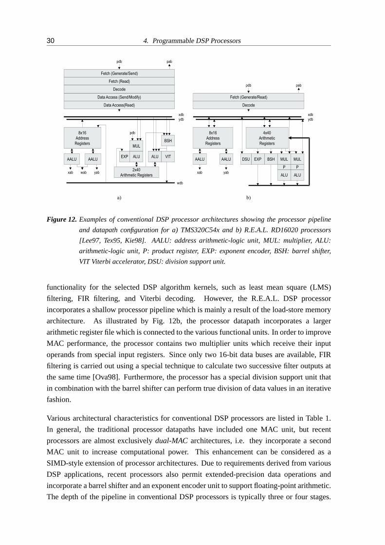
30 4. Programmable DSP Processors
xdb
ydb
yab
pdb pab
xab
a) b)
pdb pab
xdb
ydb
yabxab wab
wdb
pdb
Fetch (Generate/Read)
8x16
Address
Registers
4x40
Arithmetic
Registers
AALU MUL MULBSHAALU
ALU ALU
Decode
EXPDSU
Fetch (Generate/Send)
Fetch (Read)
8x16
Address
Registers
2x40
Arithmetic Registers
AALU
BSH
AALUALU
Data Access (Send/Modify)
Data Access(Read)
Decode
VITALUEXP
MUL
P P
Figure 12. Examples of conventional DSP processor architectures showing the processor pipeline
and datapath configuration for a) TMS320C54x and b) R.E.A.L. RD16020 processors
[Lee97, Tex95, Kie98]. AALU: address arithmetic-logic unit, MUL: multiplier, ALU:
arithmetic-logic unit, P: product register, EXP: exponent encoder, BSH: barrel shifter,
VIT Viterbi accelerator, DSU: division support unit.
functionality for the selected DSP algorithm kernels, such as least mean square (LMS)
filtering, FIR filtering, and Viterbi decoding. However, the R.E.A.L. DSP processor
incorporates a shallow processor pipeline which is mainly a result of the load-store memory
architecture. As illustrated by Fig. 12b, the processor datapath incorporates a larger
arithmetic register file which is connected to the various functional units. In order to improve
MAC performance, the processor contains two multiplier units which receive their input
operands from special input registers. Since only two 16-bit data buses are available, FIR
filtering is carried out using a special technique to calculate two successive filter outputs at
the same time [Ova98]. Furthermore, the processor has a special division support unit that
in combination with the barrel shifter can perform true division of data values in an iterative
fashion.
Various architectural characteristics for conventional DSP processors are listed in Table 1.
In general, the traditional processor datapaths have included one MAC unit, but recent
processors are almost exclusively dual-MAC architectures, i.e. they incorporate a second
MAC unit to increase computational power. This enhancement can be considered as a
SIMD-style extension of processor architectures. Due to requirements derived from various
DSP applications, recent processors also permit extended-precision data operations and
incorporate a barrel shifter and an exponent encoder unit to support floating-point arithmetic.
The depth of the pipeline in conventional DSP processors is typically three or four stages.
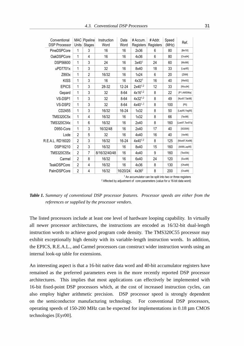
4.3. Conventional DSP Processors 31
MAC
Units
1
1
1
1
1
1
1
1
1
1
1
1
2
2
2
2
2
2
2
Pipeline
Stages
3
4
3
3
2
3
3
3
3
4
6
3
5
3
3
7
8
4
4
Instruction
Word
16
16
24
32
16/32
16
28-32
32
16/32
16/32
16/32
16/32/48
32
16/32
16/32
8/16/32/40/48
16/32
16/32
16/32
Data
Word
Conventional
DSP Processor
PineDSPCore
OakDSPCore
DSP56600
uPD7701x
Z893x
KISS
EPICS
VS-DSP1
CD2455
TMS320C5x
TMS320C54x
D950-Core
Lode
R.E.A.L. RD16020
Carmel
TeakDSPCore
PalmDSPCore
TMS320C55x
DSP16210
16
16
16
16
16-24
16
16
16
16
16/20/24
16-24
8-64
12-24
16
16
16
16
16
16
# Accum.
Registers
2x36
4x36
3x401
8x40
1x24
4x321
2x401,2
4x321,2
1x32
1x32
2x40
2x40
4x40
4x401,2
4x40
6x40
4x36
4x362
8x40
# Addr.
Registers
6
6
24
18
6
16
12
8
8
8
8
17
16
8
15
9
24
8
8
Ref.
[Be’93]
[Ova94]
[Mot96]
[Lap95]
[Zil99]
[Wei92]
[Wou94]
[Nur97,Tak98]
[Lap95,Yag95]
[Tex98]
[Lee97,Tex97a]
[SGS95]
[Ver96]
[Moe97,Kie98]
[Ali98,Lap95]
[Tex00b]
[Suc98]
[Oha99]
[Ova99]
1 An accumulator can be split into two or three registers2 Affected by adjustment of core parameters (value for a 16-bit data word)
Speed
(MHz)
66
160
40
40
125
160
160
120
130
200
50
49
33
40
20
33
60
80
80
1 3 32VS-DSP2 8-64 4x401,2 8 [P5]100
1 3 32Gepard 8-64 4x161,2 8 [P1,AMS98a]22
Table 1. Summary of conventional DSP processor features. Processor speeds are either from the
references or supplied by the processor vendors.
The listed processors include at least one level of hardware looping capability. In virtually
all newer processor architectures, the instructions are encoded as 16/32-bit dual-length
instruction words to achieve good program code density. The TMS320C55 processor may
exhibit exceptionally high density with its variable-length instruction words. In addition,
the EPICS, R.E.A.L., and Carmel processors can construct wider instruction words using an
internal look-up table for extensions.
An interesting aspect is that a 16-bit native data word and 40-bit accumulator registers have
remained as the preferred parameters even in the more recently reported DSP processor
architectures. This implies that most applications can effectively be implemented with
16-bit fixed-point DSP processors which, at the cost of increased instruction cycles, can
also employ higher arithmetic precision. DSP processor speed is strongly dependent
on the semiconductor manufacturing technology. For conventional DSP processors,
operating speeds of 150-200 MHz can be expected for implementations in 0.18 µm CMOS
technologies [Eyr00].
32 4. Programmable DSP Processors
4.4 VLIW DSP Processors
In conventional DSP processors various architectural enhancements must undergo careful
analysis to find whether the added features are justified in terms of the implementation
cost and increased complexity to the processor. While increasing performance and
application-specific features, an enhanced processor architecture should remain backwards
code compatible, which is often very difficult to realize. In addition, due to non-orthogonal
ISAs, conventional DSP processors are a difficult target for software compilation using
high-level languages.
To address these issues, several DSP processors based on the VLIW design philosophy
have emerged quite recently [Far98]. The key concepts behind VLIW DSP processors are
characterized by orthogonal instruction sets, code generation with compilers, and very high
performance through increased instruction-level parallelism. As opposed to conventional
DSP processors, these processors provide increased performance and ease of use at the
expense of higher implementation cost and power consumption. Generally, VLIW DSP
processors are deployed in computationally demanding communications systems, such as
cellular base stations, digital subscriber loop modems, cable modems, digital satellite
receivers, and high-definition television sets.
In order to simplify instruction decoding and support wide issue, old VLIW machines use a
fixed-sized instruction word whose length is typically between 64 and 256 bits, thus resulting
in poor program code density. VLIW DSP processors, however, employ simple but efficient
compression techniques to encode no-operation instructions in the unused VLIW issue slots.
In effect, these compressed VLIW instructions are issue packets which are specified at
program compile-time. During program execution VLIW DSP processors identify these
issue packets and conceptually reconstruct the full-length VLIW instruction words. From
an architectural point of view, it is arguable if this type of multiple-issue processor should
actually be referred to as compiler-scheduled superscalar rather than VLIW.
Therefore, the program execution in typical VLIW DSP processors is based on pipelined
execution of compressed VLIW instruction words. These instruction words are composed
of a number of atomic instructions which typically have a fixed length but may also
have a dual-length format [Roz99]. When compared with the operation of conventional
DSP processors, the instruction pipeline realizes wide program memory fetches, identifies
and decodes a set of parallel atomic instructions, and dispatches them to the execution
pipeline. Often the execution pipeline consists of several stages for performing
operations in a pipelined fashion. In general, VLIW DSP processors use a load-store
memory architecture and avoid pipeline interlocking and forwarding by using multi-cycle
no-operation instructions because this significantly reduces the complexity of the processor
implementation.
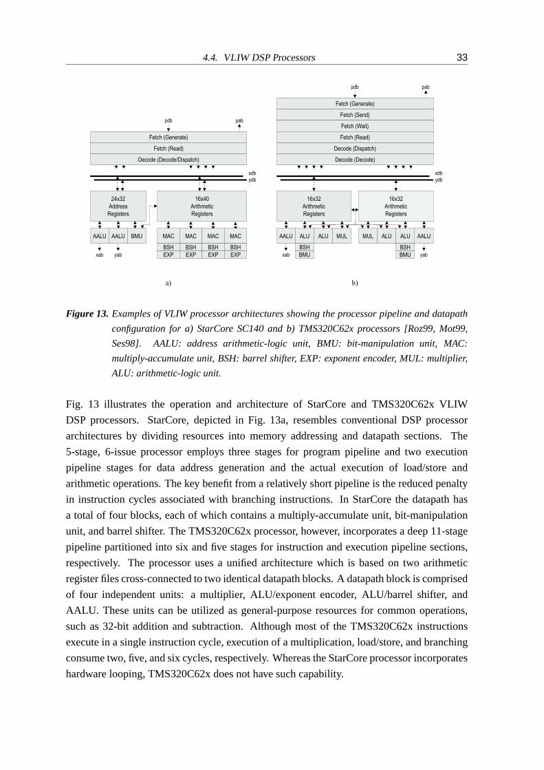
4.4. VLIW DSP Processors 33
xdb
ydb
yab
pdb pab
xab
16x32
Arithmetic
Registers
xab yab
xdb
ydb
a) b)
pdb pab
Fetch (Generate)
24x32
Address
Registers
Fetch (Read)
Decode (Decode/Dispatch)
16x40
Arithmetic
Registers
AALU MAC MAC MAC MAC
BSH
BMUAALU
BSH BSH BSH
EXP EXP EXP EXP
Fetch (Generate)
Decode (Dispatch)
Decode (Decode)
Fetch (Send)
Fetch (Wait)
Fetch (Read)
16x32
Arithmetic
Registers
AALU ALU ALU MUL MUL ALU
BSH
BMU
AALUALU
BSH
BMU
Figure 13. Examples of VLIW processor architectures showing the processor pipeline and datapath
configuration for a) StarCore SC140 and b) TMS320C62x processors [Roz99, Mot99,
Ses98]. AALU: address arithmetic-logic unit, BMU: bit-manipulation unit, MAC:
multiply-accumulate unit, BSH: barrel shifter, EXP: exponent encoder, MUL: multiplier,
ALU: arithmetic-logic unit.
Fig. 13 illustrates the operation and architecture of StarCore and TMS320C62x VLIW
DSP processors. StarCore, depicted in Fig. 13a, resembles conventional DSP processor
architectures by dividing resources into memory addressing and datapath sections. The
5-stage, 6-issue processor employs three stages for program pipeline and two execution
pipeline stages for data address generation and the actual execution of load/store and
arithmetic operations. The key benefit from a relatively short pipeline is the reduced penalty
in instruction cycles associated with branching instructions. In StarCore the datapath has
a total of four blocks, each of which contains a multiply-accumulate unit, bit-manipulation
unit, and barrel shifter. The TMS320C62x processor, however, incorporates a deep 11-stage
pipeline partitioned into six and five stages for instruction and execution pipeline sections,
respectively. The processor uses a unified architecture which is based on two arithmetic
register files cross-connected to two identical datapath blocks. A datapath block is comprised
of four independent units: a multiplier, ALU/exponent encoder, ALU/barrel shifter, and
AALU. These units can be utilized as general-purpose resources for common operations,
such as 32-bit addition and subtraction. Although most of the TMS320C62x instructions
execute in a single instruction cycle, execution of a multiplication, load/store, and branching
consume two, five, and six cycles, respectively. Whereas the StarCore processor incorporates
hardware looping, TMS320C62x does not have such capability.

34 4. Programmable DSP Processors
Pipeline
Stages
5
11
11
7
353
8
Atomic
Instr. Word
VLIW
Width
128
256
256
224
81
128
16/32/48
32
32
44
81
32
Ref.
[Roz99,Mot99]
Packed
Data Types
8/16/32
8/16/32
8/16/32
8/16/32
9/18/36
8/16/32
Issue
Width
6
8
8
5
6
4
Data
Buses
2x64
2x32
2x64
2x32
11x72
2x128
VLIW DSP Processor
StarCore SC140
TMSC62x
TMS320C64x
TriMedia TM-1100
MPact 21
TigerSharc ADSP-TS0011
16x16
MACs
4
2
4
8
44
8
[Ses98,Tex97b]
[Tex00c]
[Rat96,Phi99]
[Owe97,Pur98]
[Fri99,Ana99]
ZSP LSI402Z2 645 16 16/32 1x6454 2 [LSI99]
1 Floating-point DSP processor2 Superscalar DSP processor
3 Length of 3D graphics rendering pipeline4 18x18 MAC operation, value estimated from data bus width
5 Width of instruction cache line
Speed
(MHz)
200
150
125
133
600
250
300
Table 2. Summary of VLIW DSP processor features. Processor speeds are either from the references
or supplied by the processor vendors.
Table 2 lists the main features of a number of VLIW DSP processors. It should be noted
that only the first four processors can be classified as fixed-point VLIW DSP processors.
Although the other three processors are either floating-point or superscalar DSP processors,
they are included for comparison purposes due to their strong fixed-point MAC performance.
Typically, VLIW DSP processors can issue six or eight atomic instructions in parallel and the
depth of the pipeline is at least five stages. The width of a decompressed VLIW instruction
is between 128 and 256 bits. In addition to VLIW compression, the StarCore processor
employs an atomic instruction word of variable-length to achieve even higher code density.
Interestingly, the StarCore architecture also supports extension instructions that can execute
various operations in tightly-coupled instruction-set accelerators.
Although a 16-bit data precision is adequate for most DSP computations, all the listed
processors support packed data types and they have wide data memory buses for realizing
high bandwidth to transfer operands for the functional units. As an example, using two 64-bit
data buses, TMS320C64x can simulataneously read a total of eight 16-bit values to perform
four 16×16-bit MAC operations in parallel. As stated earlier, processor speeds are dependent
on the semiconductor manufacturing technology. For VLIW DSP processors, operating
speeds of 250-300 MHz can be expected for 0.18 µm CMOS technologies [Roz99, Tex00c].

5. CUSTOMIZABLE FIXED-POINT DSP PROCESSOR CORE
This chapter presents a fixed-point DSP processor core that has been utilized in the research
work covered in most of the publications. General architecture, main features, and various
implementation aspects of both hardware and software are described.
5.1 Background
The DSP processor presented in this chapter has evolved through three generations. The
first processor architecture, named Gepard, was presented in [P1, P2] and [Gie97]. This
initial processor architecture established the base architecture template that incorporates
a customizable DSP processor core with the modified Harvard memory architecture. The
second and third core, referred to here as VS-DSP1 and VS-DSP2, employed a slightly
different set of parameters and gradually added various enhancements to the processor
operation primarily by optimizing the structure of the functional units [Nur97],[P5].
The DSP processor was targeted for use as an embedded processor core in highly integrated
DSP systems that are integrated into a single silicon die. The processor development aimed
at designing a DSP core architecture which combines a flexible processor architecture with
an efficient hardware implementation by using optimized transistor-level circuit compilers
[Nur94]. The DSP processor has a customizable architecture that has a native support for
adjustment of a wide range of core parameters and it also allows straightforward extension
of the instruction set. These customization capabilities can be exploited to characterize the
processor ISA to match the exact needs of a given application [P1]. In the past, similar
DSP processor architectures have been reported, for example in [Wou94, Yag95]. These
processors, however, were either based on a different implementation approach or they
allowed only a limited degree of customization.
5.2 Architecture
In order to support extensive processor customization, the DSP processor employs an
architecture that allows changes to a specified set of core parameters. Thus from an
embedded system developer’s point of view, this parameterized DSP processor can be viewed

36 5. Customizable Fixed-Point DSP Processor Core
DSP Processor Core
ctrl
xab
yab
Program
Control
Unit
Program
Memory
Datapath
Data
Address
Generator
X Data
Memory
Y Data
Memory
iab
xdb
ydbidb
Figure 14. Base architecture of the customizable fixed-point DSP processor. The DSP processor
core is composed of three main units: Program Control Unit, Datapath, and Data
Address Generators. The processor core is connected to three off-core memories with
the associated address (iab,xab,yab) and data (idb,xdb,ydb) buses.
as a family of DSP processors that share a common base architecture rather than a single
processor that has fixed functional characteristics and architecture. The base architecture of
the DSP processor, depicted in Fig. 14, is composed of three main functional units: Program
Control Unit, Datapath, and Data Address Generator. The DSP processor core connects
to the separate program memory, two data memories, and off-core peripheral units using
three global buses, each with its associated data, address, and control bus. Core parameters
available in all the three implemented DSP processors are the following: data word width,
multiplier operand width, number of accumulator guard bits, number of arithmetic and
address registers, data and program address widths, program word width, and the depth of the
hardware looping. In this text these parameters are referred to as dataword, multiplierwidth,
multiplierguardbits, accumulators, indexregs, dataaddress, programaddress, programword,
and loopregs.
In these DSP processor cores, program execution is based on the scalar pipelined instruction
issue scheme found in conventional DSP processors. Instructions are encoded into a 32-bit
instruction word. The width of the instruction word is a core parameter, programword, but
it is not likely to change without very definitive grounds. Although the instruction word
is relatively wide, it has at least two main benefits from the instruction-set architecture
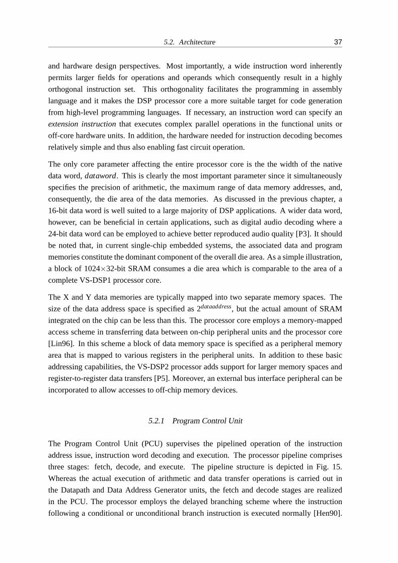
5.2. Architecture 37
and hardware design perspectives. Most importantly, a wide instruction word inherently
permits larger fields for operations and operands which consequently result in a highly
orthogonal instruction set. This orthogonality facilitates the programming in assembly
language and it makes the DSP processor core a more suitable target for code generation
from high-level programming languages. If necessary, an instruction word can specify an
extension instruction that executes complex parallel operations in the functional units or
off-core hardware units. In addition, the hardware needed for instruction decoding becomes
relatively simple and thus also enabling fast circuit operation.
The only core parameter affecting the entire processor core is the the width of the native
data word, dataword. This is clearly the most important parameter since it simultaneously
specifies the precision of arithmetic, the maximum range of data memory addresses, and,
consequently, the die area of the data memories. As discussed in the previous chapter, a
16-bit data word is well suited to a large majority of DSP applications. A wider data word,
however, can be beneficial in certain applications, such as digital audio decoding where a
24-bit data word can be employed to achieve better reproduced audio quality [P3]. It should
be noted that, in current single-chip embedded systems, the associated data and program
memories constitute the dominant component of the overall die area. As a simple illustration,
a block of 1024×32-bit SRAM consumes a die area which is comparable to the area of a
complete VS-DSP1 processor core.
The X and Y data memories are typically mapped into two separate memory spaces. The
size of the data address space is specified as 2dataaddress, but the actual amount of SRAM
integrated on the chip can be less than this. The processor core employs a memory-mapped
access scheme in transferring data between on-chip peripheral units and the processor core
[Lin96]. In this scheme a block of data memory space is specified as a peripheral memory
area that is mapped to various registers in the peripheral units. In addition to these basic
addressing capabilities, the VS-DSP2 processor adds support for larger memory spaces and
register-to-register data transfers [P5]. Moreover, an external bus interface peripheral can be
incorporated to allow accesses to off-chip memory devices.
5.2.1 Program Control Unit
The Program Control Unit (PCU) supervises the pipelined operation of the instruction
address issue, instruction word decoding and execution. The processor pipeline comprises
three stages: fetch, decode, and execute. The pipeline structure is depicted in Fig. 15.
Whereas the actual execution of arithmetic and data transfer operations is carried out in
the Datapath and Data Address Generator units, the fetch and decode stages are realized
in the PCU. The processor employs the delayed branching scheme where the instruction
following a conditional or unconditional branch instruction is executed normally [Hen90].

38 5. Customizable Fixed-Point DSP Processor Core
Fetch
Address
Registers
Arithmetic
Registers
AALU
xdb
ydb
yab
idb iab
xab
Decode
Additional
Functional
Unit
AALU Datapath
Figure 15. Pipeline structure of the customizable fixed-point DSP processor. Processor architecture
supports extension instructions which perform application-specific arithmetic and
addressing operations in the processor core and in additional functional units. AALU:
address arithmetic-logic unit.
Thus the processor pipeline is visible to the programmer. In these processors, an instruction
cycle corresponds to one processor clock cycle. Pipeline interlocking is not needed
since all the instructions effectively execute in one clock cycle. However, the interrupt
dispatch mechanism requires a selective cancellation of an instruction being processed in
the processor pipeline [P4].
The principal structure of the PCU is depicted in Fig. 16. As a result of instruction decoding,
two groups of control signals are generated: execution and flow control. The execution
control signals are used to initiate various operations in the main functional units and
off-core peripherals. The flow control signals, however, are solely utilized by the Instruction
Address Generator (IAG). With the aid of condition status flags, hardware looping control
IR
xdbydb
idbInstruction
Decode
Instruction
Address
Generator
Interrupt
Controlinterrupt
Control
Registers
execution
ctrl iab
condition
flags
Looping
Hardware
flow
ctrl
reset
Figure 16. Functional block diagram of the Program Control Unit. IR: instruction register.
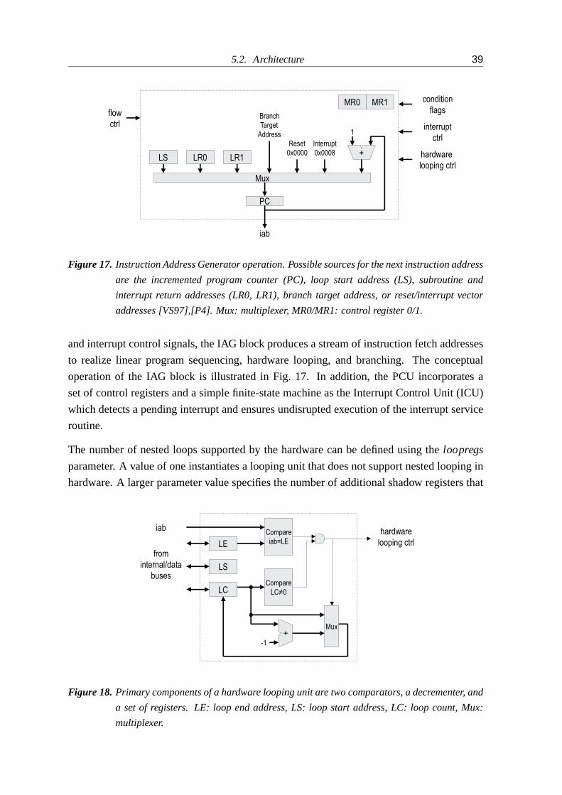
5.2. Architecture 39
PC
1
Mux
Reset
0x0000
Interrupt
0x0008
Branch
Target
Address
LR1LR0LS
iab
flow
ctrl
condition
flagsMR0 MR1
interrupt
ctrl
hardware
looping ctrl
+
Figure 17. Instruction Address Generator operation. Possible sources for the next instruction address
are the incremented program counter (PC), loop start address (LS), subroutine and
interrupt return addresses (LR0, LR1), branch target address, or reset/interrupt vector
addresses [VS97],[P4]. Mux: multiplexer, MR0/MR1: control register 0/1.
and interrupt control signals, the IAG block produces a stream of instruction fetch addresses
to realize linear program sequencing, hardware looping, and branching. The conceptual
operation of the IAG block is illustrated in Fig. 17. In addition, the PCU incorporates a
set of control registers and a simple finite-state machine as the Interrupt Control Unit (ICU)
which detects a pending interrupt and ensures undisrupted execution of the interrupt service
routine.
The number of nested loops supported by the hardware can be defined using the loopregs
parameter. A value of one instantiates a looping unit that does not support nested looping in
hardware. A larger parameter value specifies the number of additional shadow registers that
LC
Mux
LE
-1
LS
Compare
iab=LE
Compare
LC≠ 0
hardware
looping ctrl
iab
from
internal/data
buses
+
Figure 18. Primary components of a hardware looping unit are two comparators, a decrementer, and
a set of registers. LE: loop end address, LS: loop start address, LC: loop count, Mux:
multiplexer.

40 5. Customizable Fixed-Point DSP Processor Core
ALU
xdbydb
Datapath
Register
File
Multiply-
Accumulate
Unit
C D
Shifter
P
Datapath
Register
File
Multiplier
Shifter
P
xdbydb
ALU
a) b)
Figure 19. Functional block diagram of the Datapaths used in a) the Gepard processor and b) the
two VS-DSP processors [P1],[Nur97]. ALU: arithmetic-logic unit, C: multiplier register,
D: multiplicand register, P: product register.
are required to store several loop end and start addresses and loop counts. A functional block
diagram of the hardware looping unit is depicted in Fig. 18. In program code a hardware loop
can be initialized with a loop instruction or the register contents can directly be manipulated
with data transfers.
5.2.2 Datapath
The primary computation engine of the DSP processor core is the Datapath unit. As
typical of the conventional DSP architectures discussed in the previous chapter, the Datapath
design follows a traditional structure based on an arithmetic-logic unit (ALU) and a
multiply-accumulate or multiplier unit, as depicted in Fig. 19. The figure shows two different
structures which correspond to the original Gepard datapath and to the modified datapath
which is employed in the two VS-DSP processors. Both structures have a pipeline register
and thus an additional instruction cycle is necessary to move the result of a multiplication
or MAC operation to the register file. In this subchapter the parameter for the multiplier
operand width, multiplierwidth, is assumed to be equal to dataword.
The Gepard datapath, shown in Fig. 19a, incorporates a MAC unit that can perform
a dataword×dataword-bit multiplication and a (multiplierguardbits + 2×dataword)-bit
addition which is stored in the product register P. In a MAC operation the multiplier operand
5.2. Architecture 41
is always the C register, but the multiplicand can be either the D register or one of the datapath
registers. In Gepard, the shifter is used to select certain bit slices from the full-precision
product register [VS96]. Using dataword wide operands, the ALU performs general-purpose
arithmetic and logical functions: addition, subtraction, absolute value, left and right shift by
one, and basic logical operations. Depending on the value of accumulators, the datapath
register file contains 2, 3, or 4 registers. The benefit of this datapath structure is that it allows
independent ALU operations in parallel with MAC computations. Unfortunately, it was later
discovered that the parallel execution of MAC/ALU operations was of limited practical use
in typical DSP algorithms.
Therefore, the later VS-DSP processor cores incorporated a new datapath structure which is
shown in Fig. 19b. The MAC operation is carried out with a (dataword +1)× (dataword +1)-bit hardware multiplier and a (multiplierguardbits + 2×dataword)-bit ALU [Nur97].
The extra bit in the hardware multiplier operands is to allow mixed operations with signed
two’s complement and unsigned binary operands. Support for multiplication with fractional
numbers is enabled by the simple shifter which, in its basic form, can only perform the
necessary logical left shift by one bit. The datapath register file contains a maximum
of eight dataword wide registers which can be grouped to compose four accumulator
registers. Optionally the register file may include additional guard bits specified by the
multiplierguardbits parameter.
5.2.3 Data Address Generator
The Data Address Generator (DAG), two types of which are depicted in Fig. 20, is capable
of issuing and post-modifying two independent data memory addresses during an instruction
cycle. The DAG incorporates two address arithmetic-logic units (AALUs) coupled with an
address register file that holds indexregs registers. Thus data memory addressing employs the
register indirect addressing mode as the basis for all data memory accesses. The addressing
mode and post-modification operation are determined either directly from an instruction
word or they are specified by an address register pair.
As a result of the load-store memory architecture the Gepard and VS-DSP processor
cores inherently support the register direct addressing mode. Additionally, the VS-DSP2
processor core realizes register-to-register data transfers. The immediate addressing is only
available as a load constant instruction. Moreover, two DSP-specific addressing modes
can be utilized: modulo (alternatively circular) and bit-reversed addressing. Both of
these addressing modes realize a special access pattern to a programmer-specified block
of memory. Modulo addressing can be used to effectively realize data structures found
in common DSP algorithms, such as FIFO buffers and delay lines [Lee88]. Bit-reversed
addressing provides a significant acceleration of data manipulations required in an N-point
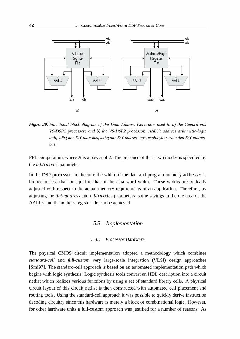
42 5. Customizable Fixed-Point DSP Processor Core
Address
Register
File
AALU AALU
xdb
ydb
xab yab
Address/Page
Register
File
AALU AALU
xdb
ydb
exab eyab
a) b)
Figure 20. Functional block diagram of the Data Address Generator used in a) the Gepard and
VS-DSP1 processors and b) the VS-DSP2 processor. AALU: address arithmetic-logic
unit, xdb/ydb: X/Y data bus, xab/yab: X/Y address bus, exab/eyab: extended X/Y address
bus.
FFT computation, where N is a power of 2. The presence of these two modes is specified by
the addrmodes parameter.
In the DSP processor architecture the width of the data and program memory addresses is
limited to less than or equal to that of the data word width. These widths are typically
adjusted with respect to the actual memory requirements of an application. Therefore, by
adjusting the dataaddress and addrmodes parameters, some savings in the die area of the
AALUs and the address register file can be achieved.
5.3 Implementation
5.3.1 Processor Hardware
The physical CMOS circuit implementation adopted a methodology which combines
standard-cell and full-custom very large-scale integration (VLSI) design approaches
[Smi97]. The standard-cell approach is based on an automated implementation path which
begins with logic synthesis. Logic synthesis tools convert an HDL description into a circuit
netlist which realizes various functions by using a set of standard library cells. A physical
circuit layout of this circuit netlist is then constructed with automated cell placement and
routing tools. Using the standard-cell approach it was possible to quickly derive instruction
decoding circuitry since this hardware is merely a block of combinational logic. However,
for other hardware units a full-custom approach was justified for a number of reasons. As
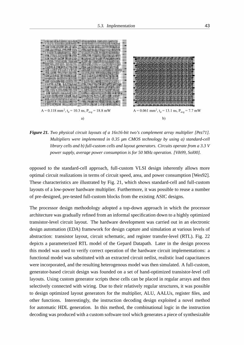
5.3. Implementation 43
a) b)
A = 0.118 mm2, td = 10.3 ns, Pavg = 18.8 mW A = 0.061 mm2, td = 13.1 ns, Pavg = 7.7 mW
Figure 21. Two physical circuit layouts of a 16x16-bit two’s complement array multiplier [Pez71].
Multipliers were implemented in 0.35 µm CMOS technology by using a) standard-cell
library cells and b) full-custom cells and layout generators. Circuits operate from a 3.3 V
power supply, average power consumption is for 50 MHz operation. [Vih99, Sol00].
opposed to the standard-cell approach, full-custom VLSI design inherently allows more
optimal circuit realizations in terms of circuit speed, area, and power consumption [Wes92].
These characteristics are illustrated by Fig. 21, which shows standard-cell and full-custom
layouts of a low-power hardware multiplier. Furthermore, it was possible to reuse a number
of pre-designed, pre-tested full-custom blocks from the existing ASIC designs.
The processor design methodology adopted a top-down approach in which the processor
architecture was gradually refined from an informal specification down to a highly optimized
transistor-level circuit layout. The hardware development was carried out in an electronic
design automation (EDA) framework for design capture and simulation at various levels of
abstraction: transistor layout, circuit schematic, and register transfer-level (RTL). Fig. 22
depicts a parameterized RTL model of the Gepard Datapath. Later in the design process
this model was used to verify correct operation of the hardware circuit implementations: a
functional model was substituted with an extracted circuit netlist, realistic load capacitances
were incorporated, and the resulting heterogenous model was then simulated. A full-custom,
generator-based circuit design was founded on a set of hand-optimized transistor-level cell
layouts. Using custom generator scripts these cells can be placed in regular arrays and then
selectively connected with wiring. Due to their relatively regular structures, it was possible
to design optimized layout generators for the multiplier, ALU, AALUs, register files, and
other functions. Interestingly, the instruction decoding design exploited a novel method
for automatic HDL generation. In this method, the combinational logic in the instruction
decoding was produced with a custom software tool which generates a piece of synthesizable
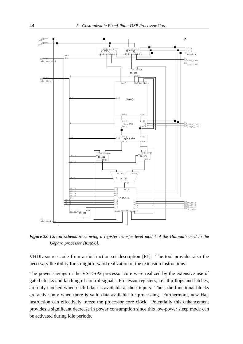
44 5. Customizable Fixed-Point DSP Processor Core
W=16
W=16
W=16
W=31
clk1
clk2
xdb
ydb
alu_reg_ctrl
alu_ctrl
alu_cond_neg
dreg_test
creg_test
pregs_testpregc_test
a3_testa2_testa1_testa0_test
reset_x
7:43:0
11:813:1215:14
0
3:1
4
6:5
14:7
16:15
18:17
20:1922:2124:2326:2527
30:28
W=16W=16
W=16cregW=4 W=16
W=16 W=16
W=16dregW=4 W=16
W=16 W=16W=40W=40
W=40 W=40
macW=3
W=40 W=40
W=40W=40preg W=40
W=40
W=2W=40W=40
W=16 W=16shift
W=16 W=16
W=8
W=16
alu
W=16
W=16W=16W=16 W=16W=16
W=4accu
W=2W=2
W=2W=2W=2
W=4
W=16W=16W=16W=16
W=2
W=16W=16
muxW=16
W=16 W=16W=2mux
W=16
W=16 W=16W=2mux
W=16
W=4W=3mux
Figure 22. Circuit schematic showing a register transfer-level model of the Datapath used in the
Gepard processor [Kuu96].
VHDL source code from an instruction-set description [P1]. The tool provides also the
necessary flexibility for straightforward realization of the extension instructions.
The power savings in the VS-DSP2 processor core were realized by the extensive use of
gated clocks and latching of control signals. Processor registers, i.e. flip-flops and latches,
are only clocked when useful data is available at their inputs. Thus, the functional blocks
are active only when there is valid data available for processing. Furthermore, new Halt
instruction can effectively freeze the processor core clock. Potentially this enhancement
provides a significant decrease in power consumption since this low-power sleep mode can
be activated during idle periods.
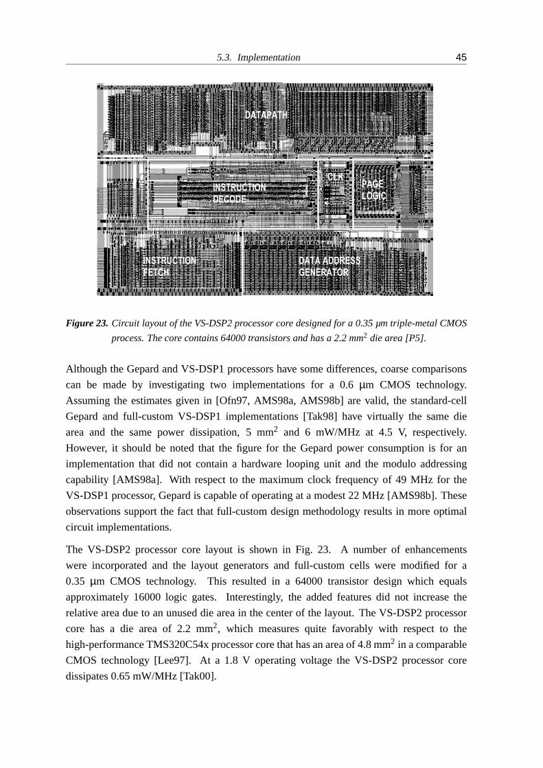
5.3. Implementation 45
INSTRUCTIONFETCH
DATA ADDRESSGENERATOR
INSTRUCTIONDECODE
DATAPATH
PAGELOGIC
CLK
Figure 23. Circuit layout of the VS-DSP2 processor core designed for a 0.35 µm triple-metal CMOS
process. The core contains 64000 transistors and has a 2.2 mm2 die area [P5].
Although the Gepard and VS-DSP1 processors have some differences, coarse comparisons
can be made by investigating two implementations for a 0.6 µm CMOS technology.
Assuming the estimates given in [Ofn97, AMS98a, AMS98b] are valid, the standard-cell
Gepard and full-custom VS-DSP1 implementations [Tak98] have virtually the same die
area and the same power dissipation, 5 mm2 and 6 mW/MHz at 4.5 V, respectively.
However, it should be noted that the figure for the Gepard power consumption is for an
implementation that did not contain a hardware looping unit and the modulo addressing
capability [AMS98a]. With respect to the maximum clock frequency of 49 MHz for the
VS-DSP1 processor, Gepard is capable of operating at a modest 22 MHz [AMS98b]. These
observations support the fact that full-custom design methodology results in more optimal
circuit implementations.
The VS-DSP2 processor core layout is shown in Fig. 23. A number of enhancements
were incorporated and the layout generators and full-custom cells were modified for a
0.35 µm CMOS technology. This resulted in a 64000 transistor design which equals
approximately 16000 logic gates. Interestingly, the added features did not increase the
relative area due to an unused die area in the center of the layout. The VS-DSP2 processor
core has a die area of 2.2 mm2, which measures quite favorably with respect to the
high-performance TMS320C54x processor core that has an area of 4.8 mm2 in a comparable
CMOS technology [Lee97]. At a 1.8 V operating voltage the VS-DSP2 processor core
dissipates 0.65 mW/MHz [Tak00].

46 5. Customizable Fixed-Point DSP Processor Core
Figure 24. Screen view of the X Window version of the instruction-set simulator [P2].
The main drawbacks of a full-custom design are technology dependence of the cell layouts
and the development time, which is relatively long. This, however, is not an issue with
synthesized hardware implementations since a design can smoothly be retargeted to nearly
any standard-cell library provided by semiconductor manufacturers. In the past, fully
synthesizable DSP processor cores have been reported for standard-cell ASIC [Wou94] and
FPGA technologies [Lah97]. The apparent ease of implementation in these DSP processors,
however, was strongly offset by poor performance and relatively high power consumption.
More recently, synthesizable DSP processors have been announced in [Oha99, Ova99]. For
the time being, it appears that logic synthesis tools are capable of producing fast hardware
circuits but are still unable to efficiently cope with some low-level physical issues, such
as power-aware synthesis of logic circuits. The DSP processor reported in [Wou94] was
later followed by a processor realization [Moe97] which actually resembles the Gepard and
VS-DSP processors from both the architecture and implementation points of view.
5.3.2 Software Tools
In addition to the hardware circuit design, the development process required a considerable
amount of software engineering effort to create software development tools for the processor
core. The first set of tools incorporated a symbolic macro assembler, a disassembler, an

5.3. Implementation 47
object file linker, and an instruction-set simulator (ISS) [P2]. In addition, a profiler tool was
later implemented which is essential for comprehensive analysis of the dynamic behavior of
the application code [P3, P4].
A graphical user interface of the ISS is shown in Fig. 24. The ISS provides a cycle-accurate
simulation engine for testing, debugging, and analysis of the application software. The
simulator also supports the parameterized architecture and it allows co-simulation using
C-language descriptions of the off-core hardware units. The ISS executes simulations in
an interpretative fashion and it achieves an execution rate of 0.25 million instructions per
second in current state-of-the-art workstations. As opposed to using code interpretation, a
compiled simulation approach could be employed to accelerate program simulation [Bar87].
In the compiled simulation approach, the program code for simulation is each time compiled
into a single executable program, effectively constructing a high-performance ISS for this
program code. Thus, the overhead from the interpretation of the code is eliminated. This
type of compiled simulation approach for DSP processors has been reported in [Ziv95],
showing a simulation speed-up by a factor of 100 to 200. More recently, this approach has
also been applied to instruction-set simulation of VLIW processors [Ahn98].
Traditionally, the application programming for a DSP processor solely relied on writing the
necessary routines in assembly language. In assembly language, the program development is
very time-consuming, programming is error-prone by nature, and the program code exhibits
poor maintainability. For the customizable DSP processor core, a major upgrade to the
software tools was introduced with a C-compiler [P5]. The developed C-compiler supports
the ANSI C-language standard and also includes a number of features which can be used to
guide code generation towards a more optimal result. It is likely, however, that a majority
of the applications will benefit from a mixed approach where a large bulk of the program
code is written in C-language and the performance-critical algorithm kernels and low-level
peripheral drivers are implemented as optimized assembly language modules. For example,
this approach was successfully applied in developing a software implementation of the
MPEG layer III audio decoder [Tak00].
Furthermore, the development environment was reinforced with a real-time operating
system (RTOS) that provides a pre-emptive multitasking kernel and a wide range of system
services for embedded applications. The services include intertask communication, memory
management, and task switching. Due to the modular structure of the RTOS, different
services can be selected to build a system kernel that contains the services needed by an
application. The RTOS was written completely in assembly language, thus resulting in a
small program memory footprint and a minimal overhead in the RTOS operation [P5]. It
should be noted, however, that a fully-featured system kernel requires a hardware system
timer as an off-core peripheral.

6. SUMMARY OF PUBLICATIONS
This chapter summarizes the seven publications included in Part II of this thesis. The
publications are divided into two categories describing the customizable fixed-point DSP
processor core and high-level specification of wireless communications systems. Whereas
this chapter highlights the primary topics in each publication, main conclusions are given in
the next chapter.
6.1 Customizable Fixed-Point DSP Processor Core
Publications [P1], [P2], [P3], [P4], and [P5] are summarized in this section. The publications
describe the evolution of the DSP processor architecture and present the development of an
audio decoder application and an analysis of a parallel program memory coupled with the
DSP processor core.
Publication [P1]: A parameterized and extensible DSP core architecture. This publication
gives the first presentation of the novel DSP processor core architecture. The Gepard
processor is the result of the research that was carried out as a joint collaboration work
at Tampere University of Technology, VLSI Solution Oy, and Austria Mikro Systeme
International AG (AMS). The early development of the DSP processor core was carried out
in 1996 and it has been reported in [Kuu96]. In relation to the other papers, this publication
contains the most detailed coverage of the Gepard processor architecture. Block diagrams
of all three main functional units are shown, the core parameters employed in this processor
version are presented, and their impact on the functional units is studied in detail. As an
application example, the customization of the Gepard architecture for a GSM full-rate speech
codec is briefly reviewed.
Publication [P2]: Flexible DSP core for embedded systems. Whereas the previous
publication was an initial presentation of the DSP processor architecture, this article gives
a more comprehensive view of a DSP processor core-based ASIC design flow. The article
focuses on the main issues associated with deployment of this licensable DSP processor in
embedded system designs. Interestingly, this publication in fact describes a system design
50 6. Summary of Publications
flow which was later introduced in the form of intellectual property (IP) usage in which
a system developer integrates a reusable hardware component as part of a larger entity.
A core-based design flow is illustrated with a figure that shows the tasks performed by
the processor core vendor and the customer, i.e. the system developer. The concept of
an extensible instruction set is presented. The processor ISA is composed of 25 basic
instructions, a parameterized number of registers and levels of hardware looping, and a
number of extension instructions. The extension instructions can be defined to allow access
to off-core peripherals or special functions embedded in the processor datapath. Software
development tools supporting the flexible ISA are presented. The application example
briefly covered in [P1] is given a more comprehensive treatment. Using four DSP processor
configurations the speech codec application is refined into an optimized implementation. The
four cases are carefully evaluated in terms of task run-times, memory usage, and estimated
die areas. In addition, comparisons of application speed-up, estimated power consumption,
and relative cost of speed-up are given.
Publication [P3]: MPEG-1 layer II audio decoder implementation for a parameterized
DSP core. This publication presents the development of a standard digital audio
decoder [ISO93] for the VS-DSP1 processor core. Conceptually, real-time audio decoding
is realized as embedded software executed in an MPEG audio decoder IC that contains a
VS-DSP1 processor core, two 16-bit audio DACs, and miscellaneous peripherals on a single
silicon die. An external flash memory device complements the decoder IC by providing
a large storage space for digital audio streams. The publication describes a systematic
implementation approach to transform a C-language source code with floating-point
arithmetic into an efficient implementation in assembly language. In order to provide
satisfactory audio quality, certain sections had to exploit extended-precision multiplication
operations, a feature that had then become available in the VS-DSP1 processor [Nur97].
Publication [P4]: A parallel program memory architecture for a DSP core. This publication
describes an experiment with the VS-DSP1 processor coupled with a memory architecture
in which the single program memory block was replaced with several parallel program
memory blocks. The rationale for the parallel program memory architecture is that, to
some extent, a potentially slow memory read access time can be compensated by fetching
multiple instruction words in parallel. A slow read access time is a characteristic of flash
memory devices which have found increasingly wide-spread use in embedded systems.
The program sequencing in the VS-DSP1 processor is presented. The publication presents
a general parallel memory architecture [Gos94] and a suitable architecture for pipelined
program execution is derived for the DSP architecture. Moreover, program code mapping
and implications on the program memory addressing are described. Memory architectures
6.2. Specification of Wireless Communications Systems 51
with 1 to 8 memory blocks were evaluated with a GSM half-rate speech codec and the audio
decoder that was implemented in [P3]. For both applications, performance was evaluated
with three cases.
Publication [P5]: Enhanced DSP core for embedded applications. The VS-DSP1
processor, utilized in Publications [P3] and [P4], was followed by the VS-DSP2 processor
core that was improved in several ways. The VS-DSP2 processor was enhanced with
several new instructions, extended program and data addressing capability, vectored interrupt
support, and a number of low-power features. The design objectives are first formulated
and justified. Then implementation of each of the enhancements and their influence on
the processor operation are studied in detail. Moreover, the publication describes two new
additions to software development environment: an optimizing C-compiler and a modular
real-time operating system. The embedded system prototyping was also reinforced with a
DSP evaluation board that can be employed for application prototyping purposes.
6.2 Specification of Wireless Communications Systems
Publications [P6] and [P7] are summarized in this Section. A dataflow simulation of a
wireless LAN system is reported and a high-level evaluation of a third-generation W-CDMA
radio transceiver is described.
Publication [P6]: Run-time configurable hardware model in a dataflow simulation. This
publication describes a system-level simulation of a wireless communication system. As
a case study, a wireless LAN system in which compressed image data is transmitted to a
number of mobile terminals is modeled and simulated [Mik96, Wal91]. Conceptually, the
mobile terminal implementation had a target architecture which integrates a DSP processor,
a microcontroller, a hardware accelerator, and a radio frequency front-end. The system
was modeled by constructing a dataflow model of the transmitter-receiver chain. The
functions were described using C-language models and the entire system was simulated
with a commercial simulation environment. Two basic transform operations were needed in
the mobile terminal: complex-valued 16-point fast Fourier transform (FFT) and a 8×8-point
inverse discrete cosine transform (IDCT). In the system, a configurable hardware accelerator,
described in VHDL code, carried out both of these transforms. The publication describes
the main system functions and time-multiplexed FFT/IDCT scheduling and reviews the
implementation of synchronous and asynchronous models which are necessary to permit
heterogenous dataflow system simulation with the event-driven HDL model of the hardware
accelerator.

52 6. Summary of Publications
Publication [P7]: Baseband implementation aspects for W-CDMA mobile terminals. This
publication presents a functional architecture of a mobile terminal transceiver that can be
employed to implement the European candidate proposal for the third-generation mobile
cellular standard [ETS98]. After a brief overview of the two operation modes specified in
the proposal, the fundamental operations in the receiver and transmitter baseband sections are
studied in detail. In this context, the term ‘baseband’ is used to refer to all the digital signal
processing that is needed in the inner receiver [Mey98]. Due to the considerably higher
complexity, the emphasis is mainly on the receiver implementation. The presented receiver
architecture is based on a conventional Rake receiver which is complemented with a number
of relatively simple functional units for tasks such as pulse shaping filtering and various
measurements. The publication includes coarse estimates of sample precision, sample rate,
and digital signal processing requirements and presents well-suited hardware structures for
the main receiver functions. Moreover, the baseband partitioning into application-specific
hardware and DSP software is briefly discussed.
6.3 Author’s Contribution to Published Work
In this section the Author’s contribution to the published work is clarified publication by
publication. The Author is the primary author in six of the seven publications. The
co-authors have seen these clarifications and agree with the Author. None of the publications
have been used as part of another person’s academic thesis or dissertation.
Publication [P1]. The initial DSP processor core architecture was developed by a team
consisting of Prof. Jari Nurmi, Janne Takala, M.Sc., Pasi Ojala, M.Sc., Henrik Herranen,
Richard Forsyth, M.Sc., and the Author. The Author was involved in the design and
simulation of a register transfer-level model of the Gepard processor core and he also
performed functional verifications on the processor operation [Kuu96]. Prof. Olli Vainio
gave valuable comments on the work.
Publication [P2]. In this publication the Author was responsible for the detailed
presentation of the licensable DSP processor. Together with Prof. Jari Nurmi and Janne
Takala, M.Sc., the concept of the DSP processor core-based ASIC design flow was solidified.
The software tools were designed by Pasi Ojala, M.Sc., and Henrik Herranen. The Author
and Prof. Jari Nurmi performed the trade-off analysis of the GSM speech codec that was
programmed by Juha Rostrom, M.Sc. This analysis is a more comprehensive study of the
preliminary results presented in [P1].
6.3. Author’s Contribution to Published Work 53
Publication [P3]. The idea of designing a standard audio decoder for the fixed-point
VS-DSP1 processor was proposed by the Author. Teemu Parkkinen, M.Sc., performed this
work under supervision of the Author [Par99]. The Author suggested the implementation
approach in which a C-language source code was gradually transformed into an assembly
language program. The main contribution was the idea of modifying the C-language
source code first to employ 16-bit fixed-point arithmetic. Thereafter assembly language
programming became a straighforward task. Prof. Jarkko Niittylahti gave valuable
comments on the work.
Publication [P4]. The idea of a parallel program memory was initially suggested by Prof.
Jarmo Takala and Prof. Jarkko Niittylahti. With the aid of a VS-DSP1 processor HDL model
provided by Janne Takala, M.Sc., the Author constructed a testbench for the parallel memory
architecture. The Author performed the analysis of the memory architecture using a GSM
speech codec programmed by Juha Rostrom, M.Sc., and the MPEG audio decoder presented
in [P3]. Prof. Jarkko Niittylahti gave valuable comments on the work.
Publication [P5]. Architectural design and low-level circuit implementation of the
VS-DSP2 processor was devised by Janne Takala, M.Sc. Based on the data provided by
him and Pasi Ojala, M.Sc., the Author carried out an extensive evaluation of enhancements
that were implemented in both the VS-DSP2 processor core and software development tools.
Pasi Ojala, M.Sc., developed the real-time operating system and also the C-compiler which
was initially referred to in [P2].
Publication [P6]. In this publication the Author designed various dataflow models and a
hierarchical block diagram of the wireless LAN system. This case study was suggested
by Prof. Jarmo Takala, who also provided an HDL model of the configurable transform
hardware. The Author developed a scheme to allow embedding of the run-time configurable
hardware model, planned operation scheduling in the receiver, and performed extensive
simulation runs to verify correct system operation. Prof. Jukka Saarinen gave valuable
comments on the work.
Publication [P7]. In order to have a solid foundation for later research, an extensive study
of CDMA receivers was performed by the Author. The Author resolved the functions
needed in a W-CDMA transceiver and drafted conceptual architectures for both receiver
and transmitter sections. Later, performance estimations in terms of MAC operations per
second were calculated and reported in [Kuu99].

7. CONCLUSIONS
The research reported in this thesis has been to a great extent applied technical research
rather than basic research. The published results address a wide range of issues which
are associated with the specification, design, and implementation of a commercially viable
DSP processor architecture. Furthermore, the research work covers specification of wireless
communication systems, an application area which clearly benefits the most from the raw
computational power, low power consumption, and instruction-set specialization provided
by modern DSP processors. In this chapter the main results are summarized and the thesis is
concluded with a discussion on future trends in wireless system design and DSP processors.
7.1 Main Results
In this thesis, the development of a flexible DSP processor core architecture has been
presented. The processor evolution encompasses three generations, all sharing the base
architecture template initially presented in [P1]. In this publication the main functional units
and core parameters for the Gepard processor were described. Using a GSM full-rate speech
codec algorithm, it was demonstrated that it is possible to improve the processor performance
by adjusting the core parameters and the features of the processor datapath.
A generic ASIC design flow for usage of the DSP processor core was shaped in [P2]. Based
on the licensable processor core approach, the steps in the system development were divided
into tasks carried out by the core vendor and the DSP system developer. In the publication,
the GSM full-rate speech codec application was given a more detailed analysis. The trade-off
analysis covered four cases beginning with a basic core and ending with an optimized core
that has a hardware looping unit, saturation mode, and add-with-carry capability. As opposed
to the basic core, the optimized core reduced the instruction cycle count by 43 % and
consequently the estimated power consumption by 37 %. Interestingly, the total die area
remained virtually the same, 17 mm2, because the area increase in the core was compensated
by the reduced program memory size.
Implementation of an MPEG audio decoder for the VS-DSP1 processor was presented
in [P3]. The decoder software was based on a systematic approach in which a floating-point
C-language source code was first converted to a version that accurately mimics 16-bit

56 7. Conclusions
fixed-point arithmetic operations. After this modification the converted C-language
source code served as a bit-accurate representation of the algorithm behavior in the DSP
processor. The implementation also illustrates the use of extended-precision 16×32-bit MAC
operations which were needed for certain parts in the decoding algorithm. The program
code required 2.3 kwords and the data memory usage was 12.4 kwords, of which 74 %
was employed for various fixed-valued data values. An extensive analysis performed on the
dynamic behavior of the application code revealed that a 25 MHz processor clock frequency
was sufficient for 192 kbit/s, 44.1 kHz stereo audio streams.
In [P4] a parallel program memory architecture was described. The proposed parallel
architecture was analyzed with a GSM speech codec and the audio decoder that was
presented in [P3]. The main problems encountered were the instruction cycle penalties
associated with branching and hardware looping. The results show that the GSM speech
codec was, in fact, quite ineffective with the memory architecture. However, due to the
highly sequential program code, the MPEG audio decoder was able to gain a linear speed-up.
From the practical point of view, memory architectures with two or four parallel memory
banks seemed to be reasonable.
In addition to improvements to the DSP processor core itself, [P5] presented several
topics emphasizing the importance of the development environment. During the course
of development, it had became clear that a bare DSP processor core is quite far from a
reusable, licensable IP component. The key area of concern for a DSP system developer
is the infrastructure provided by a DSP processor core vendor. Before committing to
a certain processor architecture, potential system developers need to be convinced that
they have access to all the support necessary to accomplish the development work. This
infrastructure contains a wide range of issues: software and hardware development tools,
operating systems, high-level EDA tools, software and algorithm libraries, and extensive
technical support. An established DSP processor core vendor has to build all the appropriate
infrastructure in place, so that system developers can immediately benefit from this
infrastructure.
Furthermore, the research covers two different approaches to high-level specification of
wireless communications systems. Currently, simulation environments based on the dataflow
paradigm have an increasingly important role in specification of complex signal processing
systems. As presented in [P6], these tools can be exploited to rapidly design an executable
system specification using a library of functional models. Later, this specification was
reused for co-verification purposes where two functional models were realized with an
implementation-level description of a multi-functional hardware unit. Although the resulting
system model was rather complicated, the simulation environment provided excellent means
for formulating system-level concepts, such as operation scheduling. Moreover, the system
simulation with the hardware unit increased the simulation time by at least two orders of
magnitude, thus distinctly demonstrating trade-offs between simulation accuracy and speed.

7.1. Main Results 57
Area(mm2)
Gepard
VS-DSP1
VS-DSP2
Power(mW/MHz @ 3.3V)
Gepard
VS-DSP1
VS-DSP2
Speed(MHz)
Gepard
VS-DSP1
VS-DSP2
5.0
5.3
2.2
22
49
100
2.7
2.2
3.2
Figure 25. Comparison of three DSP processor core versions. For Gepard, the area estimate is based
on a gate-level netlist and the power consumption is for a processor that does not contain
hardware looping and modulo addressing. [AMS98b, Ofn97, Tak98],[P5].
Publication [P7] presented a high-level feasibility study of the system functions and various
implementation aspects associated with a W-CDMA radio transceiver. The emphasis
was on the receiver baseband implementation which, as opposed to the transmitter,
possesses considerably higher complexity. In the publication, first impressions are
given of the conceptual partitioning into functions realized as software executed by a
high-performance DSP processor or as dedicated hardware units. As concluded, a W-CDMA
transceiver will mainly be hardware-based for functions performed at sample and chip rates.
However, a high-performance DSP processor (or processors) can provide the flexibility and
computational power needed for the operations at the symbol rates.
To conclude, the research work has satisfied the objectives of the research. A customizable
DSP processor architecture was developed and successfully implemented as three core
versions. The Gepard processor had a die area, maximum operating speed, and power
consumption of 5 mm2, 22 MHz, and 2.7 mW/MHz at 3.3 V, respectively [AMS98b, Ofn97].
The corresponding figures were 5.3 mm2, 49 MHz, and 6 mW/MHz at 4.5 V for the
VS-DSP1 processor [Tak98] and 2.2 mm2, 100 MHz, and 0.65 mW/MHz at 1.8 V for
the VS-DSP2 processor [P5]. Compared to the VS-DSP1, the VS-DSP2 implementation
demonstrates a 100 % increase in performance while the power consumption was reduced
by a factor of 9. These characteristics were mainly achieved by the shift from 0.6 µm to
0.35 µm CMOS process. Furthermore, the VS-DSP2 processor incorporated other valuable
functionality, such as the low-power idle mode and new instructions [P5]. In Fig. 25 the
Gepard, VS-DSP1, and VS-DSP2 processor cores are compared with respect to the core
area, power consumption at 3.3 V, and maximum operating speed. It should be noted that
this Gepard processor was a soft core, but the VS-DSP processors were implemented as
hard cores.
58 7. Conclusions
The customizable DSP processor architecture has proven its commercial viability
in a number of DSP-based applications, such as MPEG audio decoding and GPS
navigation [Tak00, VS00, VS99]. In the future, the VS-DSP processors will be further
improved. One of the main considerations is to improve program code density by replacing
the relatively wide 32-bit instruction word with a dual-length instruction word. Lastly, a soft
core version of the VS-DSP2 processor is currently under development.
7.2 Future Trends
Wireless communications system design will be an increasingly complex task. As the
number of transistors integrated on a single chip is rapidly escalating, platform integrators
are faced with new problems associated with system complexity, hardware/software
co-simulation speed, interconnect-dominated delays, and testability. In addition, emerging
wireless products, such as third-generation mobile phones, will require significantly more
hardware and processing power which, in turn, leads to higher implementation cost and
power consumption.
Potential scalability of VLIW DSP processors may also have its advantages for DSP
algorithms that can effectively benefit from the parallel datapath resources. However,
it seems that the next level of raising computational performance will be heavily based
on task-level parallelism. Increased parallelism is enabled by integrating multiple DSP
processor cores into an on-chip multiprocessor. The problems associated with this approach
are linked to, among others, the system partitioning, scheduling, intercore communication,
and the programming model which may be quite peculiar.
As a brief market overview, there seem to be two key players in the conventional DSP
processor arena at the moment. The DSP Group, with PineDSPCore-based family of cores,
has licensed its cores to more than 25 major system design and ASIC companies. At the
other extreme, Texas Instruments TMS320C54x, or LEAD2, has acquired a solid position
in wireless products. The company has claimed that over 60 % of mobile phones are based
on this processor [Tex00a], which implies that the C54x core could be considered as an
embedded DSP counterpart to the x86-based microprocessors.
Backwards compatibility in DSP processor families is an important issue because system
developers have a considerable amount of intellectual property associated with optimized
software. In contrast to general-purpose microcontrollers, exact binary compatibility may
not be necessary, because if an assembly language source code can just be reassembled,
the software can easily be retargeted to a new processor. This approach was taken in the
presented customizable DSP processor concept.

7.2. Future Trends 59
Emerging hardware technologies and architectures may also prove their effectiveness in
the near future. For example, reconfigurable hardware has the potential for providing
energy-efficient, run-time reusable computation engines for DSP applications [Rab97,
Zha00]. However, reconfigurable hardware needs proper EDA tools for developing such
systems in order to be a viable solution. The speed of the context switches between
various configurations is also an open question. In addition, there are indications that
application-specific instruction-set processors (ASIPs) will have a more important role in
future designs [Gat00, Kuu99]. It is imaginable that a properly designed VLIW ASIP
might be an effective component if the application area is narrow and clearly specified.
Interestingly, the presented customizable DSP processor could be exploited for such
purposes as well. Embedded DRAM (eDRAM) will be an interesting option. Compared
with conventional SRAM, six to eight times the bit density is available for the same area
using eDRAM [Iye99]. On the downside, the use of a mixed logic/DRAM process slows
down logic circuits, which may not be affordable in most systems.
Admittedly, despite the many technological aspects and intricacies discussed in this thesis,
their significance will ultimately become transparent in the finished product. Users of
commercial electronics will continue to disregard how many transistors have been integrated,
or which of the advanced CMOS technologies has been utilized, or even how many
programmable processors their new purchase contains. They will simply consider those
state-of-the-art devices as handy gadgets. It has been said: “Any sufficiently advanced
technology is indistinguishable from magic”. Nevertheless, we all profit from current
research into areas like embedded DSP processor cores, as technology convergence resulting
from the evolution of the system-on-a-chip methodology gives rise to all the conceivable
benefits ranging from reduced power requirements to smaller product size and weight and
more importantly lower product cost. This essentially summarizes what will make the
development, design, and implementation of future systems such an exciting task.

BIBLIOGRAPHY
[Ahl98] L. Ahlin and J. Zander, Principles of Wireless Communications, Studentlitteratur,
Lund, Sweden, 1998.
[Ahn98] J.-W. Ahn, S.-M. Moon, and W. Sung, “An efficient compiled simulation system
for VLIW code verification,” in Proc. 31st Annual Simulation Symposium, Boston,
MA, U.S.A., Apr. 5-9 1998, pp. 91–95.
[Ali98] M. Alidina, G. Burns, C. Holmquist, E. Morgan, D. Rhodes, S. Simanapalli, and
M. Thierbach, “DSP16000: a high performance, low power dual-MAC DSP
core for communications applications,” in Proc. IEEE Custom Integrated Circuits
Conference, Santa Clara, CA, U.S.A., May 11–14 1998, pp. 119–122.
[Alp93] D. Alpert and D. Avnon, “Architecture of the Pentium microprocessor,” IEEE
Micro Magazine, vol. 13, no. 3, pp. 11–21, June 1993.
[AMS98a] Austria Mikro Systeme International, AG, Embedded Software Programmable
DSP Core GEP 02, Preliminary datasheet, Mar. 25 1998.
[AMS98b] Austria Mikro Systeme International, AG, Embedded Software Programmable
DSP Core GEP 03, Datasheet, Mar. 25 1998.
[Ana99] Analog Devices, Inc., ADSP-TS001 Preliminary Data Sheet, Dec. 1999.
[ANS85] ANSI/IEEE Std 754-1985, “IEEE standard for binary floating-point arithmetic,”
Standard, The Institute of Electrical and Electronics Engineers, Inc., New York,
NY, U.S.A., Aug. 1985.
[ARM95] Advanced RISC Machines, Inc., ARM7TDMI, Datasheet, ARM DDI 0029E,
Aug. 1995.
[Bar87] Z. Barzilai, J. L. Carter, B. K. Rosen, and J. D. Rutledge, “HSS - A high-speed
simulator,” IEEE Trans. on Computer Aided Design of Integrated Circuits and
Systems, vol. CAD-6, no. 4, pp. 601–617, July 1987.
[Bar91] B. Barrera and E. A. Lee, “Multirate signal processing in Comdisco’s SPW,” in
Proc. IEEE Int. Conference on Acoustics, Speech, and Signal Processing, Toronto,
Canada, Apr. 14-17 1991, vol. 2, pp. 1113–1116.
62 Bibliography
[Bar96] H. Barad, B. Eitan, K. Gottlieb, M. Gutman, N. Hoffman, O. Lempel, A. Peleg,
and U. Weiser, “Intel’s multimedia architecture extension,” in Proc. Convention of
Electrical and Electronics Engineers in Israel, Jerusalem, Israel, Nov. 5-6 1996,
pp. 148–151.
[Bat88] A. Bateman and W. Yates, Digital Signal Processing System Design, Pitman
Publishing, London, United Kingdom, 1988.
[Be’93] Y. Be’ery, S. Berger, and B.-S. Ovadia, “An application-specific DSP for portable
applications,” in VLSI Signal Processing, IV, L. D. J. Eggermont, P. Dewilde,
E. Deprettere, and J. van Meerbergen, Eds., pp. 48–56. IEEE Press, New York,
NY, U.S.A., 1993.
[Bet97] M. R. Betker, J. S. Fernando, and S. P. Whalen, “The history of the
microprocessor,” Bell Labs Technical Journal, pp. 29–56, Autumn 1997.
[Bid95] E. Bidet, D. Castelain, C. Joanblanq, and P. Senn, “A fast single-chip
implementation of 8192 complex point FFT,” IEEE Journal of Solid-State
Circuits, vol. 30, no. 3, pp. 300–305, Mar. 1995.
[Bod81] J. R. Boddie, G. T. Daryanani, I. I. Eldumiati, R. N. Gadenz, and J. S. Thompson,
“Digital signal processor: Architecture and performance,” Bell System Technical
Journal, vol. 60, no. 7, pp. 1449–1462, Sep. 1981.
[Bog96] A. J. P. Bogers, M. V. Arends, R. H. J. De Haas, R. A. M. Beltman, R. Woudsma,
and D. Wettstein, “The ABC chip: Single chip DECT baseband controller based
on EPICS DSP core,” in Proc. Int. Conference on Signal Processing Applications
and Technology, Boston, MA, U.S.A., Oct. 7-10 1996.
[Bru98] D. M. Bruck, H. Yosub, Y. Itkin, Y. Gold, E. Baruch, M. Rafaeli, G. Hazan,
S. Shperber, M. Yosefin, L. Faibish, B. Branson, T. Baggett, and K. Porter, “The
DSP56652 dual core processor,” in Proc. Int. Conference on Signal Processing
Applications and Technology, Toronto, Canada, Sep. 13-16 1998.
[Buc91] J. Buck, S. Ha, E. A. Lee, and D. G. Messerschmitt, “Multirate signal processing
in Ptolemy,” in Proc. IEEE Int. Conference on Acoustics, Speech, and Signal
Processing, Toronto, Canada, Apr. 14-17 1991, vol. 2, pp. 1245–1248.
[Cam96] R. Camposano and J. Wilberg, “Embedded system design,” Design Automation
for Embedded Systems, vol. 1, no. 1, pp. 5–50, Jan. 1996.
[Cha87] B. W. Char, K. G. Geddes, G. M. Gonnet, and S. M. Watt, MAPLE Reference
Manual, Watcom Publications, Waterloo, Canada, 1987.
Bibliography 63
[Cha95] A. P. Chandrakasan and R. W. Brodersen, Low Power Digital CMOS Design,
Kluwer Academic Publishers, Menlo Park, CA, U.S.A., Apr. 1995.
[Cha96] W.-T. Chang, A. Kalavade, and E. A. Lee, Effective Heterogenous Design and
Co-Simulation, Kluwer Academic Publishers, Dordrecht, The Netherlands, 1996.
[Cha99] H. Chang, L. Cooke, M. Hunt, G. Martin, A. McNelly, and L. Todd, Surviving
the SOC Revolution: A Guide to Platform-Based Design, Kluwer Academic
Publishers, Menlo Park, CA, U.S.A., 1999.
[Che98] S.-K. Cheng, R.-M. Shiu, and J. J.-J. Shann, “Decoding unit with high issue rate
for x86 superscalar microprocessors,” in Proc. Int. Conference on Parallel and
Distributed Systems, Dec. 14-16 1998, pp. 488–495.
[Cla76] T. A. C. M. Claasen, W. F. G. Mecklenbrauker, and J. B. H. Peek, “Effects of
quantization and overflow in recursive digital filters,” IEEE Trans. on Acoustics,
Speech and Signal Processing, vol. 24, no. 6, pp. 517–529, Dec. 1976.
[DM99] G. De Micheli, “Hardware synthesis from C/C++ models,” in Proc. Design,
Automation and Test Europe Conference, Munich, Germany, Mar. 9-12 1999, pp.
382–383.
[Eri92] A. C. Erickson and B. S. Fagin, “Calculating the FHT in hardware,” IEEE Trans.
on Signal Processing, vol. 40, no. 6, pp. 1341–1353, June 1992.
[ETS92] ETSI 300 175, “Radio Equipment and Systems (RES); Digital European Cordless
Telecommunications (DECT); Common Interface; Parts 1 to 9,” International
Standard, European Telecommunications Standards Institute, Sophia Antipolis,
France, Oct. 1992.
[ETS98] ETSI Tdoc SMG2 260/98, “The ETSI UMTS terrestrial radio access
(UTRA) ITU-R RTT candidate submission,” Preliminary standard, European
Telecommunications Standards Institute, Sophia Antipolis, France, May/June
1998.
[Eyr00] J. Eyre and J. Bier, “The evolution of DSP processors,” IEEE Signal Processing
Magazine, vol. 17, no. 2, pp. 43–51, Mar. 2000.
[Far98] P. Faraboschi, G. Desoli, and J. A. Fischer, “The latest word in digital and media
processing,” IEEE Micro Magazine, vol. 15, no. 2, pp. 59–85, Mar. 1998.
[Fet91] G. Fettweis and H. Meyr, “High-speed parallel Viterbi decoding: Algorithm and
VLSI-architecture,” IEEE Communications Magazine, vol. 29, no. 5, pp. 46–55,
May 1991.
64 Bibliography
[Fri99] J. Fridman and W. C. Anderson, “A new parallel DSP with short-vector memory
architecture,” in Proc. IEEE Int. Conference on Acoustics, Speech, and Signal
Processing, Phoenix, AZ, U.S.A., Mar. 15-19 1999, vol. 4, pp. 2139–2142.
[Ful98] S. Fuller, Motorola’s AltiVec Technology, White paper, Motorola, Inc., Aug. 20
1998.
[Gaj95] D. D. Gajski and F. Vahid, “Specification and design of embedded
hardware-software systems,” IEEE Design & Test of Computers Magazine, vol.
12, no. 1, pp. 53–67, Spring 1995.
[Gat00] A. Gatherer, T. Stetzler, M. McMahan, and E. Auslander, “DSP-based
architectures for mobile communications: Past, present and future,” IEEE
Communications Magazine, vol. 38, no. 1, pp. 84–90, Jan. 2000.
[Gho99] A. Ghosh, J. Kunkel, and S. Liao, “Hardware synthesis from C/C++,” in Proc.
Design, Automation and Test Europe Conference, Munich, Germany, Mar. 9-12
1999, pp. 387–389.
[Gie97] A. Gierlinger, R. Forsyth, and E. Ofner, “GEPARD: A parameterizable DSP
core for ASICs,” in Proc. Int. Conference on Signal Processing Applications and
Technology, San Diego, CA, U.S.A., Sep. 14-17 1997, pp. 203–207.
[Gol99] M. Golden, S. Hesley, A. Scherer, M. Crowley, S. C. Johnson, S. Meier, D. Meyer,
J. D. Moench, S. Oberman, H. Partovi, F. Weber, S. White, T. Wood, and J. Yong,
“A seventh-generation x86 microprocessor,” IEEE Journal of Solid-State Circuits,
vol. 34, no. 11, pp. 1466–1477, Nov. 1999.
[Gon99] D. R. Gonzales, “Micro-RISC architecture for the wireless market,” IEEE Micro
Magazine, vol. 19, no. 4, pp. 30–37, July-Aug. 1999.
[Goo95] G. Goossens, D. Lanneer, M. Pauwels, F. Depuydt, K. Schoofs, A. Kifli, P. Petroni,
F. Catthoor, M. Cornero, and H. De Man, “Integration of medium-throughput
signal processing algorithms on flexible instruction-set architectures,” Journal of
VLSI Signal Processing, vol. 9, no. 1/2, pp. 49–65, Jan. 1995.
[Goo97] G. Goossens, J. Van Praet, D. Lanneer, W. Geurts, A. Kifli, C. Liem, and P. G.
Paulin, “Embedded software in real-time signal processing systems: Design
technologies,” Proceedings of the IEEE, vol. 85, no. 3, pp. 436–454, Mar. 1997.
[Gos94] M. Gossel, B. Rebel, and R. Creutzburg, Memory Architecture & Parallel Access,
Elsevier Science, Amsterdam, the Netherlands, 1994.
Bibliography 65
[Gre95] D. Greenley, J. Bauman, D. Chang, D. Chen, R. Eltejaein, P. Ferolito, P. Fu,
R. Garner, D. Greenhill, H. Grewal, K. Holdbrook, B. Kim, L. Kohn, H. Kwan,
M. Levitt, G. Maturana, D. Mrazek, C. Narasimhaiah, K. Normoyle, N. Parveen,
P. Patel, A. Prabhu, M. Tremblay, M. Wong, L. Yang, K. Yarlagadda, R. Yu,
R. Yung, and G. Zyner, “UltraSPARC: The next generation superscalar 64-bit
SPARC,” in IEEE Compcon ’95, Digest of Papers, San Francisco, CA, U.S.A.,
Mar. 5–9 1995, pp. 319–326.
[Gut92] G. Guttag, R. J. Gove, and J. R. Van Aken, “A single-chip multiprocessor for
multimedia: The MVP,” IEEE Computer Graphics & Applications, pp. 53–64,
Nov. 1992.
[Hag82] Y. Hagiwara, Y. Kita, T. Miyamoto, Y. Toba, H. Hara, and T. Akazawa, “A single
chip digital signal processor and its application to real-time speech analysis,”
IEEE Trans. on Acoustics, Speech and Signal Processing, vol. ASSP-16, no. 1,
pp. 339–346, Feb. 1982.
[Ham97] L. Hammond, B. A. Nayfeh, and K. Olukotun, “A single-chip multiprocessor,”
IEEE Computer Magazine, vol. 30, no. 9, pp. 79–85, Sep. 1997.
[Hen90] J. L. Hennessy and D. A. Patterson, Computer Architecture: A Quantitative
Approach, Morgan Kauffman Publishers, San Mateo, CA, U.S.A., 1990.
[Hen96] H. Hendrix, “Viterbi decoding in the TMS320C54x family,” Application note
SPRA071, Texas Instruments, Inc., Dallas, TX, U.S.A., June 1996.
[Heu97] V. P. Heuring and H. F. Jordan, Computer Systems Design and Architecture,
Kluwer Academic Publishers, Menlo Park, CA, U.S.A., Apr. 1997.
[Hwa79] K. Hwang, Computer Arithmetic: Principles, Architecture and Design, John
Wiley & Sons, Ltd., New York, U.S.A., 1979.
[Hwa85] K. Hwang and F. A. Briggs, Computer Architecture and Parallel Processing,
McGraw-Hill Book Co., Singapore, 1985.
[IEE87] IEEE Std 1076-1987, “IEEE Standard VHDL Language Reference Manual,”
Standard, The Institute of Electrical and Electronics Engineers, Inc., New York,
NY, U.S.A., Mar. 31 1987.
[Ife93] E. C. Ifeachor and B. W. Jervis, Digital Signal Processing: A Practical Approach,
Addison Wesley Longman, Inc., Menlo Park, CA, U.S.A., 1993.
[ISO93] ISO/IEC 11172-3, “Information technology - Coding of moving pictures and
associated audio for digital storage media at up to about 1.5 Mbit/s - Part 3:

66 Bibliography
Audio,” International standard, International Organization for Standardization,
Geneva, Switzerland, Mar. 1993.
[Iye99] S. S. Iyer and H. L. Kalter, “Embedded DRAM technology: Opportunities and
challenges,” IEEE Spectrum, vol. 36, no. 4, pp. 56–64, Apr. 1999.
[Joe94] O. J. Joeressen and H. Meyr, “Hardware ‘in the loop’ simulation with COSSAP:
Closing the verification gap,” in Proc. Int. Conference on Signal Processing
Applications and Technology, Dallas, TX, U.S.A., Oct. 18-21 1994.
[Joh91] W. M. Johnson, Superscalar Processor Design, Prentice Hall, Englewood Cliffs,
NJ, U.S.A., 1991.
[Kal96] K. Kalliojarvi and J. Astola, “Roundoff errors in block-floating-point systems,”
IEEE Trans. on Signal Processing, vol. 44, no. 4, pp. 783–790, Apr. 1996.
[Ken97] A. R. Kennedy, M. Alexander, E. Fiene, J. Lyon, B. Kuttanna, R. Patel, M. Pham,
M. Putrino, C. Croxton, S. Litch, and B. Burgess, “A G3 PowerPC superscalar
low-power microprocessor,” in Proc. IEEE Compcon, San Jose, CA, U.S.A., Feb.
23-26 1997, pp. 315–324.
[Kes98] R. E. Kessler, E. J. McLellan, and D. A. Webb, “The Alpha 21264 microprocessor
architecture,” in Proc. Int. Conference on Computer Design, Oct. 5-7 1998, pp.
90–95.
[Kie98] P. Kievits, E. Lambers, C. Moerman, and R. Woudsma, “R.E.A.L. DSP technology
for telecom baseband processing,” in Proc. Int. Conference on Signal Processing
Applications and Technology, Toronto, Canada, Sep. 13-16 1998.
[Kla00] A. Klaiber, The Technology behind Crusoe Processors, White paper, Transmeta
Corp., Jan. 2000.
[Knu97] J. Knuutila and T. Leskinen, “System requirements of wireless terminals for future
multimedia applications,” in Proc. European Multimedia, Microprocessor Systems
and Electronic Commerce Conference, Florence, Italy, Nov. 1997, pp. 658–665.
[Knu99] J. Knuutila, On the Development of Multimedia Capabilities for Wireless
Terminals, Dr.Tech. Thesis, Tampere University of Technology, Tampere, Finland,
May 1999.
[Kop97] H. Kopetz, Real-Time Systems Design Priciples for Distributed Embedded
Applications, Kluwer Academic Publishers, Norwell, MA, U.S.A., 1997.
[Kum97] A. Kumar, “The HP-PA-8000 RISC CPU,” IEEE Micro Magazine, vol. 17, no. 2,
pp. 27–32, Mar./Apr. 1997.
Bibliography 67
[Kur98] I. Kuroda and T. Nishitani, “Multimedia processors,” Proceedings of the IEEE,
vol. 86, no. 6, pp. 1203–1221, June 1998.
[Kur99] I. Kuroda, “RISC, video and media DSPs,” in Digital Signal Processing for
Multimedia Systems, K. K. Parhi and T. Nishitani, Eds., pp. 245–272. Marcel
Dekker, Inc., New York, NY, U.S.A., 1999.
[Kut99] K. Kutaragi, M. Suzuoki, T. Hiroi, H. Magoshi, S. Okamoto, M. Oka, A. Ohba,
Y. Yamamoto, M. Furuhashi, M. Tanaka, T. Yutaka, T. Okada, M. Nagamatsu,
Y. Urakawa, M. Funyu, A. Kunimatsu, H. Goto, K. Hashimoto, N. Ide,
H. Murakami, Y. Ohtaguro, and A. Aono, “A microprocessor with a 128b CPU,
10 floating-point MACs, 4 floating-point dividers, and an MPEG2 decoder,” in
IEEE Int. Solid-State Circuits Conference, Digest of Tech. Papers, San Francisco,
CA, U.S.A., Feb. 15-17 1999, pp. 256–257.
[Kuu96] M. Kuulusa, Modelling and Simulation of a Parameterized DSP Core, M.Sc.
Thesis, Tampere University of Technology, Tampere, Finland, 1996.
[Kuu99] M. Kuulusa and J. Nurmi, “SCREAM Q4 report: W-CDMA baseband
performance estimations,” Technical report, Tampere University of Technology,
Tampere, Finland, Oct. 1999.
[Lah97] J. Lahtinen and L. Lipasti, “Development of a 16 bit DSP core processor using
FPGA prototyping,” in Proc. Int. Conference on Signal Processing Applications
and Technology, San Diego, CA, U.S.A., Sep. 14-17 1997.
[Lap95] P. D. Lapsley, J. C. Bier, A. Shoham, and E. A. Lee, Buyer’s Guide to DSP
Processors, Berkeley Design Technology, Inc., Fremont, CA, U.S.A., 1995.
[Lap96] P. D. Lapsley, J. Bier, A. Shoham, and E. A. Lee, DSP Processor Fundamentals:
Architectures and Features, Berkeley Design Technology, Inc., Fremont, CA,
U.S.A., 1996.
[Lee88] E. A. Lee, “Programmable DSP architectures: Part I,” IEEE ASSP Magazine, vol.
5, no. 4, pp. 4–19, Oct. 1988.
[Lee90a] E. A. Lee, “Programmable DSPs: A brief overview,” IEEE Micro Magazine, vol.
10, no. 5, pp. 14–16, Oct. 1990.
[Lee90b] J. C. Lee, E. Cheval, and J. Gergen, “The Motorola 16-bit DSP ASIC core,”
in Proc. IEEE Int. Conference on Acoustics, Speech, and Signal Processing,
Albuquerque, New Mexico, Apr. 3-6 1990, vol. II, pp. 973–976.
[Lee94] E. A. Lee and D. G. Messerschmitt, Digital Communication, Kluwer Academic
Publishers, Menlo Park, CA, U.S.A., 1994.
68 Bibliography
[Lee95] R. B. Lee, “Accelerating multimedia with enhanced microprocessors,” IEEE
Micro Magazine, vol. 15, no. 2, pp. 22–32, Apr. 1995.
[Lee97] W. Lee, P. E. Landman, B. Barton, S. Abiko, H. Takahashi, H. Mizuno,
S. Muramatsu, K. Tashiro, M. Fusumada, L. Pham, F. Boutaud, E. Ego, G. Gallo,
H. Tran, C. Lemonds, A. Shih, R. H. Eklund, and I. C. Chen, “A 1-V
programmable DSP for wireless communications,” IEEE Journal of Solid-State
Circuits, pp. 1766–1776, Nov. 1997.
[Lie94] C. Liem, T. May, and P. Paulin, “Instruction-set matching and selection for DSP
and ASIP code generation,” in Proc. European Design and Test Conference, Paris,
France, Feb. 28-Mar. 3 1994, pp. 31–37.
[Lin96] B. Lin, S. Vercauteren, and H. De Man, “Embedded architecture co-synthesis
and system integration,” in Proc. Int. Workshop on Harware/Software Codesign,
Pittsburgh, PA, U.S.A., Mar. 18-20 1996, pp. 2–9.
[LSI99] LSI Logic Corp., ZSP Digital Signal Processor Architecture, Technical manual,
Sep. 1999.
[Mag82] S. Magar, E. Claudel, and A. Leigh, “A microcomputer with digital signal
processing capability,” in IEEE Int. Solid-State Circuits Conference, Digest of
Tech. Papers, Feb. 1982, pp. 32–33, 284–285.
[Mey98] H. Meyr, M. Moeneclaey, and S.A. Fechtel, Digital Communications Receivers:
Synchronization, Channel Estimation, and Signal Processing, John Wiley & Sons,
Inc., New York, NY, U.S.A., 1998.
[Mik96] J. Mikkonen and J. Kruys, “The Magic WAND: A wireless ATM access system,”
in Proc. ACTS Mobile Summit, Granada, Spain, Nov. 1996, pp. 535–542.
[Moe97] K. Moerman, P. Kievits, E. Lambers, and R. Woudsma, “R.E.A.L. DSP:
Reconfigurable embedded DSP architecture for low-power/low-cost applications,”
in Proc. Int. Conference on Signal Processing Applications and Technology, San
Diego, CA, U.S.A., Sep. 14-17 1997.
[Mol88] C. Moler, “MATLAB - A mathematical visualization laboratory,” in Proc. IEEE
Compcon, San Francisco, CA, U.S.A., Feb. 29-Mar. 3 1988, pp. 480–481.
[Mot96] Motorola, Inc., DSP56600 16-bit Digital Signal Processor Family Manual, User’s
manual, DSP56600FM/AD, 1996.
[Mot99] Motorola, Inc., Lucent Technologies, Inc., SC140 DSP Core, Preliminary
reference manual, MNSC140CORE/D, Dec. 1999.
Bibliography 69
[Nic78] W. E. Nicholson, R. W. Blasco, and K. R. Reddy, “The S2811 signal processing
peripheral,” in Proc. WESCON, 1978, vol. 25/3, pp. 1–12.
[Nis81] T. Nishitani, R. Maruta, Y. Kawakami, and H. Goto, “Digital signal processor:
Architecture and performance,” IEEE Journal of Solid-State Circuits, vol. SC-16,
no. 4, pp. 372–376, Aug. 1981.
[Nok99] Nokia Corp., Nokia’s Financial Statements 1999, Annual report, 1999.
[Nur94] J. Nurmi, Application Specific Digital Signal Processors: Architecture and
Transferable Layout Design, Dr.Tech. Thesis, Tampere University of Technology,
Tampere, Finland, Dec. 1994.
[Nur97] J. Nurmi and J. Takala, “A new generation of parameterized and extensible DSP
cores,” in Proc. IEEE Workshop on Signal Processing Systems, M. K. Ibrahim,
P. Pirsch, and J. McCanny, Eds., pp. 320–329. IEEE Press, New York, NY, U.S.A.,
Nov. 3-5 1997.
[Obe99] S. Oberman, G. Favor, and F. Weber, “AMD 3DNow! technology: Architecture
and implementations,” IEEE Micro Magazine, vol. 19, no. 2, pp. 37–48, Mar./Apr.
1999.
[Ofn97] E. Ofner, R. Forsyth, and A. Gierlinger, “GEPARD, ein parammetrisierber DSP
Kern fur ASICs,” in Proc. DSP Deutschland, Munich, Germany, Sep. 1997, pp.
176–180, in German.
[Oha99] I. Ohana and B.-S. Ovadia, “TeakDSPCore - New licensable DSP core using
standard ASIC methodology,” in Proc. Int. Conference on Signal Processing
Applications and Technology, Orlando, FL, U.S.A., Nov. 1–4 1999.
[Oja98] T. Ojanpera and R. Prasad, Wideband CDMA for Third Generation Mobile
Communications, Artech House, Boston, MA, U.S.A., 1998.
[Olu96] K. Olukotun, B. A.Nayfeh, L. Hammond, K. Wilson, and K. Chang, “The case for
a single chip multiprocessor,” in Proc. Int. Conference on Architectural Support
for Programming Languages and Operating Systems, Cambridge, MA, U.S.A.,
Oct. 1-4 1996, pp. 2–11.
[Opp89] A. V. Oppenheim and R. W. Schafer, Discrete-Time Signal Processing,
Prentice-Hall, Englewood Cliffs, NJ, U.S.A., 1989.
[Ova94] B.-S. Ovadia and Y. Be’ery, “Statistical analysis as a quantitative basis for DSP
architecture design,” in VLSI Signal Processing, VII, J. Rabaey, P.M. Chau, and
J. Eldon, Eds., pp. 93–102. IEEE Press, New York, NY, U.S.A., 1994.

70 Bibliography
[Ova98] B.-S. Ovadia, W. Gideon, and E. Briman, “Multiple and parallel execution units
in digital signal processors,” in Proc. Int. Conference on Signal Processing
Applications and Technology, Toronto, Canada, Sep. 13-16 1998, pp. 1491–1497.
[Ova99] B.-S. Ovadia and G. Wertheizer, “PalmDSPCore - Dual MAC and parallel
modular architecture,” in Proc. Int. Conference on Signal Processing Applications
and Technology, Orlando, FL, U.S.A., Nov. 1–4 1999.
[Owe97] R. E. Owen and S. Purcell, “An enhanced DSP architecture for the seven
multimedia functions: the Mpact 2 media processor,” Proc. IEEE Workshop on
Signal Processing Systems, pp. 76–85, Nov. 3-5 1997.
[Par92] D. Parsons, The Mobile Radio Propagation Channel, Pentech Press Publishers,
London, United Kingdom, 1992.
[Par99] T. Parkkinen, Digitaalisen audiodekooderin toteutus, M.Sc. Thesis, Tampere
University of Technology, Tampere, Finland, 1999, in Finnish.
[Pel96] A. Peleg and U. Weiser, “MMX technology extension for the Intel architecture,”
IEEE Micro Magazine, vol. 16, no. 4, pp. 42–50, Aug. 1996.
[Pez71] S. D. Pezaris, “A 40-ns 17-bit by 17-bit array multiplier,” IEEE Trans. on
Computers, vol. 20, pp. 442–447, Apr. 1971.
[Phi99] Philips Electronics North America Corp., TriMedia TM-110 Data Book, July
1999.
[Pro95] J. G. Proakis, Digital Communications, McGraw-Hill Book Co., Singapore, 1995.
[Pur98] S. Purcell, “The impact of Mpact 2,” IEEE Micro Magazine, vol. 15, no. 2, pp.
102–107, Mar. 1998.
[Rab72] L. R. Rabiner, “Terminology in digital signal processing,” IEEE Trans. on Audio
and Electroacoustics, vol. 20, no. 1-5, pp. 322–337, Dec. 1972.
[Rab97] J. M. Rabaey, “Reconfigurable processing: The solution to low-power
programmable DSP,” in Proc. IEEE Int. Conference on Acoustics, Speech, and
Signal Processing, Munich, Germany, Apr. 21–24 1997, pp. 275–278.
[Rat96] S. Rathnam and G. Slavenburg, “An architectural overview of the programmable
multimedia processor, TM-1,” in IEEE Compcon ’96, Digest of Papers, Santa
Clara, CA, U.S.A., Feb. 25–28 1996, pp. 319–326.
[Rat98] S. Rathnam and G. Slavenburg, “Processing the new world of interactive media -
The Trimedia VLIW CPU architecture,” IEEE Signal Processing Magazine, vol.
15, no. 2, pp. 108–117, Mar. 1998.
Bibliography 71
[Reg94] D. Regenold, “A single-chip multiprocessor DSP solution for communications
applications,” in Proc. IEEE Int. ASIC Conference and Exhibit, Rochester, NY,
U.S.A., Sep. 19-23 1994, pp. 437–440.
[Roz99] Z. Rozenshein, M. Tarrab, Y. Adelman, A. Mordoh, Y. Salant, U. Dayan,
O. Norman, K. L. Kloker, Y. Ronen, J. Gergen, B. Lindsley, P. D’Arcy, and
M. Betker, “StarCore 100 - A scalable, compilable, high-performance architecture
for DSP applications,” in Proc. Int. Conference on Signal Processing Applications
and Technology, Orlando, FL, U.S.A., Nov. 1–4 1999.
[Sch91] U. Schmidt and K. Caesar, “Datawave: A single-chip multiprocessor for video
applications,” IEEE Micro Magazine, vol. 11, no. 3, pp. 22–94, June 1991.
[Sch98] M. Schlett, “Trends in embedded-microprocessor design,” IEEE Micro Magazine,
vol. 31, no. 8, pp. 44–49, Aug. 1998.
[Sem00] L. Semeria and A. Ghosh, “Methodology for hardware/software co-verification
in C/C++,” in Proc. Asia and South Pacific Design Automation Conference,
Yokohama, Japan, Jan. 25-28 2000, pp. 405–408.
[Ses98] N. Seshan, “High VelociTI processing,” IEEE Signal Processing Magazine, vol.
15, no. 2, pp. 86–101, 117, Mar. 1998.
[SGS95] SGS-Thomson Microelectronics, Inc., D950-CORE, Preliminary specification,
Jan. 1995.
[Smi97] M. J. S. Smith, Application-Specific Integrated Circuits, Addison Wesley
Longman, Inc., Reading, MA, U.S.A., 1997.
[Sol00] T. Solla and O. Vainio, “Reusable full custom layout generators in ASIC design
flow,” Unpublished paper, 2000.
[Sri88] S. Sridharan and G. Dickman, “Block floating point implementation of digital
filters using the DSP56000,” Microprocessors and Microsystems, vol. 12, no. 6,
pp. 299–308, July/Aug. 1988.
[Suc98] R. Sucher, N. Niggebaum, G. Fettweiss, and A. Rom, “CARMEL - A new
high performance DSP core using CLIW,” in Proc. Int. Conference on Signal
Processing Applications and Technology, Toronto, Canada, Sep. 13-16 1998.
[Tak98] J. Takala, Design and Implementation of a Parameterized DSP Core, M.Sc.
Thesis, Tampere University of Technology, Tampere, Finland, 1998.

72 Bibliography
[Tak00] J. Takala, J. Rostrom, T. Vaaraniemi, H. Herranen, and P. Ojala, “A low-power
MPEG audio layer III decoder IC with an integrated digital-to-analog converter,”
in IEEE Conference on Consumer Electronics, Digest of Technical Papers, Los
Angeles, CA, U.S.A., June 13-15 2000, pp. 260–261.
[Teu98] C. M. Teuscher, Low Power Receiver Design for Portable RF Applications:
Design and Implementation of an Adaptive Multiuser Detector for an Indoor,
Wideband CDMA Application, Ph.D. Thesis, University of California, Berkeley,
CA, U.S.A., Jul. 1998.
[Tex95] Texas Instruments, Inc., TMS320C54x User’s Guide, SPRU131B, Oct. 1995.
[Tex97a] Texas Instruments, Inc., TMS320C54x - Low-Power Enhanced Architecture
Device, Workshop notes, Feb. 1997.
[Tex97b] Texas Instruments, Inc., TMS320C6201, TMS320C6201B Digital Signal Proces-
sors, Datasheet, SPRS051D, Jan. 1997.
[Tex98] Texas Instruments, Inc., TMS320C5x User’s Guide, SPRU056D, June 1998.
[Tex00a] Texas Instruments, Inc., TI Breaks Industry’s DSP High Performance and Low
Power Records with New Cores, Press release, Feb. 22 2000.
[Tex00b] Texas Instruments, Inc., TMS320C55x DSP CPU Reference Guide, Preliminary
draft, Feb. 2000.
[Tex00c] Texas Instruments, Inc., TMS320C64x Technical Overview, SPRU395, Feb. 2000.
[Tho91] D. E. Thomas and P. R. Moorby, The Verilog Hardware Description Language,
Kluwer Academic Publishers, Dordrecht, The Netherlands, 1991.
[Tre96] M. Tremblay, J. M. O’Connor, V. Narayanan, and L. He, “VIS speeds media
processing,” IEEE Micro Magazine, vol. 16, no. 4, pp. 10–20, Aug. 1996.
[Tul95] D. M. Tullsen, S. J. Eggers, and H. M. Levy, “Simultaneous multithreading:
Maximizing on-chip parallelism,” in Proc. Annual Int. Symposium on Computer
Architecture, Santa Margherita Ligure, Italy, June 22-24 1995, pp. 392–403.
[vdP94] R. van de Plassche, Integrated Analog-to-Digital and Digital-to-Analog
Converters, Kluwer Academic Publishers, Norwell, MA, U.S.A., 1994.
[Ver96] I. Verbauwhede, M. Touriguian, K. Gupta, J. Muwafi, K. Yick, and G. Fettweis, “A
low power DSP engine for wireless communications,” in VLSI Signal Processing,
IX, W. Burleson, K. Konstantinides, and T. Meng, Eds., pp. 471–480. IEEE Press,
New York, NY, U.S.A., 1996.

Bibliography 73
[Vih99] K. Vihavainen, P. Perala, and O. Vainio, “Estimation of energy consumption
using logic synthesis and simulation,” Technical report, 6-1999, Signal Processing
Laboratory, Tampere University of Technology, Tampere, Finland, 1999.
[Vit67] A. J. Viterbi, “Error bounds for convolutional coding and an asymptotically
optimum decoding algorithm,” IEEE Trans. on Information Theory, vol. 13, pp.
260–269, Apr. 1967.
[VS96] VLSI Solution Oy and Austria Mikro Systeme International AG, Gepard
Architecture and Instruction Set Specification, Revision 1.3, Feb. 1996.
[VS97] VLSI Solution Oy, VS-DSP Specification Document, Revision 0.8, Nov. 1997.
[VS99] VLSI Solution Oy, GPS Receiver Chipset, Datasheet, Version 1.1, Mar. 1999.
[VS00] VLSI Solution Oy, VS1001 - MPEG Audio Codec, Datasheet, Version 2.11, May
2000.
[Wal91] K. Wallace, “The JPEG image compression standard,” Communications of the
ACM, pp. 30–45, Apr. 1991.
[Wei92] D. Weinsziehr, H. Ebert, G. Mahlich, J. Preissner, H. Sahm, J.M. Schuck,
H. Bauer, K. Hellwig, and D. Lorenz, “KISS-16V2: A one-chip ASIC DSP
solution for GSM,” IEEE Journal of Solid-State Circuits, vol. 27, no. 7, pp.
1057–1066, July 1992.
[Wes92] N. H. E. Weste and K. Eshraghian, Principles of CMOS VLSI Circuit Design,
Addison Wesley Longman, Inc., Reading, MA, U.S.A., 1992.
[Wil63] J. H. Wilkinson, Rounding Errors in Algebraic Processes, Prentice-Hall,
Englewood Cliffs, NJ, U.S.A., 1963.
[Wou94] R. Woudsma, R. A. M. Beltman, G. Postuma, A. C. Turley, W. Brouwer,
U. Sauvagerd, B. Strassenburg, D. Wettstein, and R. K. Bertschmann, “EPICS,
a flexible approach to embedded DSP cores,” in Proc. Int. Conference on Signal
Processing Applications and Technology, Dallas, TX, U.S.A., Oct. 18-21 1994,
vol. I, pp. 506–511.
[Yag95] H. Yagi and R. E. Owen, “Architectural considerations in a configurable DSP core
for consumer electronics,” in VLSI Signal Processing, VIII, T. Nishitani and K. K.
Parhi, Eds., pp. 70–81. IEEE Press, New York, NY, U.S.A., 1995.
[Zha00] H. Zhang, V. Prabhu, V. George, M. Wan, M. Benes, A. Abnous, and
J. Rabaey, “A 1V heterogeneous reconfigurable processor IC for baseband
74 Bibliography
wireless applications,” in IEEE Int. Solid-State Circuits Conference, Digest of
Tech. Papers, San Francisco, CA, U.S.A., Feb. 6-10 2000.
[Zil99] Zilog, Inc., Z89223/273/323/373 16-bit Digital Signal Processors with A/D
Converter, Product specification, DS000202-DSP0599, 1999.
[Ziv95] V. Zivojnovic, S. Tijang, and Meyr H., “Compiled simulation of programmable
DSP architectures,” in VLSI Signal Processing, V, T. Nishitani and K. K. Parhi,
Eds., pp. 187–196. IEEE Press, New York, NY, U.S.A., 1995.

Part II
PUBLICATIONS


PUBLICATION 1
M. Kuulusa and J. Nurmi, “A parameterized and extensible DSP core architecture,” in Proc.
Int. Symposium on IC Technology, Systems & Applications, Singapore, Sep. 10–12 1997,
pp. 414–417.
Copyright c©1997 Nanyang Technological University, Singapore. Reprinted, with
permission, from the proceedings of ISIC’97.


1. INTRODUCTION
The emerging of the powerful digital signalprocessing (DSP) cores has revolutionized the conven-tional application-specific integrated circuit (ASIC)design. An ASIC is no longer assembled exclusivelyfrom in-house design, but often composed of a selectedDSP core and a bunch of hand-picked peripherals.
A DSP core acts as the primary engine for asignal processing system, providing all the necessaryfundamental arithmetic operations, data memoryaddressing, and program control for the DSP applica-tion at hand. The attractive point in utilizing DSP coresis their programmability combined with the benefits ofthe custom circuits [1]. Memories, peripherals, and cus-tom logic is embedded together with a DSP core toachieve a highly integrated, low cost solution.
DSP cores are provided as synthesizable HDL,layout, or both [2]. In general, DSP cores have fixedarchitecture which may cause excess performance,extra cost, or less efficient use of resources in someapplications. Popular choices for DSP cores includeTexas Instruments TMS320C2xx/TMS320C54x, SGS-Thomson D950-CORE, and Analog Devices ADSP-21cspxx [3]. Vendors provide these cores as standardlibrary components for their silicon technologies.Freedom of choice in the fabrication of the chip ispreserved when DSP cores are licensed. Cores of thiscategory are Clarkspur Design CD2450 and DSP GroupPine/OakDSPCore. Still, common to all of these coresis their non-existent or very limited parameterization ofthe DSP core itself.
Other DSP cores of interest are Philips EPICS[4] and REAL [5] which have more sophisticated coreparameters, but are by no means offered to customers ina broad fashion.
2. FLEXIBLE CORE-BASED APPLICATIONDEVELOPMENT
The drawbacks of traditional DSP cores can beaddressed by a flexible core that has parameters to tailorthe actual implementation to match the application aswell as possible. The optimal values for the parameterscan be discovered in software development tools sup-porting the implementation parameters. The applicationdeveloper does not even need to know the hardwarevery thoroughly, since the dependence of the imple-mentation features upon the parameters can beexpressed in a very straightforward manner. The fea-tures of importance include physical geometry (the sizeof the core and the attached memories), maximumclock rate applicable, and relative power consumption.These are easily added to the understanding of a DSPsoftware developer, besides the traditional measuressuch as number of code lines, data memory allocationand number of cycles to execute.
In our core architecture, the parameterization israther extensive. Word lengths in different blocks of thecore can be configured separately, and different levelsof features can be included by changing the type of var-ious units all over the architecture. All the numerousflavors of the implementation are supported by a singletool set, consisting of an assembler, a linker, anarchiver, and a cycle-based instruction level simulator.The tools have been programmed in generic ANSI-C tosupport multiple platforms including PC/Windows95,Sun/Solaris, and HP/HP-UX. There also exists a graph-ical user interface for the UNIX X-windows version.
In addition to the parameterization, there areextension mechanisms built into the architecture. User-specific instructions and the corresponding hardwarecan be added to the basic core. These hardware-soft-ware trade-offs to achieve the specified performance,memory sizes and circuit area can be made by the DSP
A PARAMETERIZED AND EXTENSIBLEDSP CORE ARCHITECTURE
Mika Kuulusa1 and Jari Nurmi2
1Signal Processing Laboratory, Tampere University of Technology,P.O. Box 553, FIN-33101 Tampere, Finland
2VLSI Solution Oy, Hermiankatu 6-8 CFIN-33720 Tampere, Finland
Abstract : In order to create a highly integrated, single-chip signal processing system, a DSP core can be used to providethe basic DSP functions for the target application. In this paper, a flexible DSP core architecture is presented. Theresources of this DSP core are fine-tuned with various parameters and extension instructions that execute application-specific operations in the arithmetic units of the DSP core and in additional functional units off-core. At first, the flexiblecore-based application development is discussed briefly. The DSP core architecture, its parameters, and the three mainfunctional blocks are described, and, finally, the benefits of this versatile DSP core are illustrated with a speech codingapplication example.
414
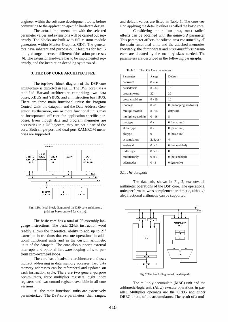
engineer within the software development tools, beforecommitting to the application-specific hardware design.
The actual implementation with the selectedparameter values and extensions will be carried out sep-arately. The blocks are built with full custom modulegenerators within Mentor Graphics GDT. The genera-tors have inherent and purpose-built features for facili-tating changes between different fabrication processes[6]. The extension hardware has to be implemented sep-arately, and the instruction decoding synthesized.
3. THE DSP CORE ARCHITECTURE
The top-level block diagram of the DSP corearchitecture is depicted in Fig. 1. The DSP core uses amodified Harvard architecture comprising two databuses, XBUS and YBUS, and an instruction bus IBUS.There are three main functional units: the ProgramControl Unit, the datapath, and the Data Address Gen-erator. Furthermore, one or more functional units maybe incorporated off-core for application-specific pur-poses. Even though data and program memories arenecessities in a DSP system, they are not a part of thecore. Both single-port and dual-port RAM/ROM mem-ories are supported.
The basic core has a total of 25 assembly lan-guage instructions. The basic 32-bit instruction word
readily allows the theoretical ability to add up to 231
extension instructions that execute operations in addi-tional functional units and in the custom arithmeticunits of the datapath. The core also supports externalinterrupts and optional hardware looping units to per-form zero-overhead loops.
The core has a load/store architecture and usesindirect addressing in data memory accesses. Two datamemory addresses can be referenced and updated oneach instruction cycle. There are two general-purposeaccumulators, three multiplier registers, eight indexregisters, and two control registers available in all coreversions.
All the main functional units are extensivelyparameterized. The DSP core parameters, their ranges,
and default values are listed in Table 1. The core ver-sion applying the default values is called the basic core.
Considering the silicon area, most radicaleffects can be obtained with the dataword parameter.This parameter affects the silicon area consumed by allthe main functional units and the attached memories.Inevitably, the dataaddress and programaddress param-eters are dictated by the memory sizes needed. Theparameters are described in the following paragraphs.
3.1. The datapath
The datapath, shown in Fig. 2, executes allarithmetic operations of the DSP core. The operationalunits perform in two’s complement arithmetic, althoughalso fractional arithmetic can be supported.
The multiply-accumulate (MAC) unit and thearithmetic-logic unit (ALU) execute operations in par-allel. Multiplier operands are the CREG and eitherDREG or one of the accumulators. The result of a mul-
Fig. 1.Top-level block diagram of the DSP core architecture(address buses omitted for clarity).
Table 1. The DSP Core parameters.
Parameter Range Default
dataword 8 - 64 16
dataaddress 8 - 23 16
programword 32 - 32
programaddress 8 - 19 16
loopregs 0 - 8 0 (no looping hardware)
multiplierwidth 8 - 64 dataword
multiplierguardbits 0 - 16 8
mactype 0 - 0 (basic unit)
shiftertype 0 - 0 (basic unit)
alutype 0 - 0 (basic unit)
accumulators 2, 3, or 4 4
enablecd 0 or 1 0 (not enabled)
indexregs 8 or 16 8
modifieronly 0 or 1 0 (not enabled)
addrmodes 0 - 3 0 ( m only)
Fig. 2.The block diagram of the datapath.
415
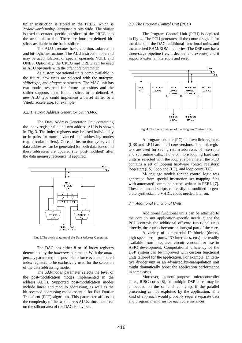
tiplier instruction is stored in the PREG, which is2*dataword+multiplierguardbits bits wide. The shifteris used to extract specific bit-slices of the PREG intothe accumulator file. There are four pre-defined bit-slices available in the basic shifter.
The ALU executes basic addition, subtractionand bit-logic instructions. The ALU instruction operandmay be accumulators, or special operands NULL andONES. Optionally, the CREG and DREG can be usedas ALU operands with the cdenable parameter.
As custom operational units come available inthe future, new units are selected with the mactype,shiftertype, and alutype parameters. The MAC unit hastwo modes reserved for future extensions and theshifter supports up to four bit-slices to be defined. Anew ALU type could implement a barrel shifter or aViterbi accelerator, for example.
3.2. The Data Address Generator Unit (DAG)
The Data Address Generator Unit containingthe index register file and two address ALUs is shownin Fig. 3. The index registers may be used individuallyor in pairs for more advanced data addressing modes(e.g. circular buffers). On each instruction cycle, validdata addresses can be generated for both data buses andthese addresses are updated (i.e. post-modified) afterthe data memory reference, if required.
The DAG has either 8 or 16 index registersdetermined by the indexregs parameter. With the modi-fieronly parameter, it is possible to force even numberedindex registers to be exclusively used for the selectionof the data addressing mode.
The addrmodes parameter selects the level ofthe post-modification modes implemented in theaddress ALUs. Supported post-modification modesinclude linear and modulo addressing, as well as thebit-reversed addressing mode essential for Fast FourierTransform (FFT) algorithm. This parameter affects tothe complexity of the two address ALUs, thus the effecton the silicon area of the DAG is obvious.
3.3. The Program Control Unit (PCU)
The Program Control Unit (PCU) is depictedin Fig. 4. The PCU generates all the control signals forthe datapath, the DAG, additional functional units, andthe attached RAM/ROM memories. The DSP core has athree-stage pipeline (fetch, decode, and execute) and itsupports external interrupts and reset.
A program counter (PC) and two link registers(LR0 and LR1) are in all core versions. The link regis-ters are used for saving return addresses of interruptsand subroutine calls. If one or more looping hardwareunits is selected with the loopregs parameter, the PCUcontains a set of looping hardware control registers:loop start (LS), loop end (LE), and loop count (LC).
M-language models for the control logic wasgenerated from special instruction set mapping fileswith automated command scripts written in PERL [7].These command scripts can easily be modified to gen-erate synthesizable VHDL codes needed later on.
3.4. Additional Functional Units
Additional functional units can be attached tothe core to suit application-specific needs. Since thePCU controls the additional off-core functional unitsdirectly, these units become an integral part of the core.
A variety of commercial IP blocks (timers,high-speed serial ports, I/O interfaces, etc.) are readilyavailable from integrated circuit vendors for use inASIC development. Computational efficiency of theDSP system can be improved with custom functionalunits tailored for the application. For example, an itera-tive divider unit or an advanced bit-manipulation unitmight dramatically boost the application performancein some cases.
Moreover, general-purpose microcontrollercores, RISC cores [8], or multiple DSP cores may beembedded on the same silicon chip, if the parallelprocessing can be exploited by the application. Thiskind of approach would probably require separate dataand program memories for each core instances.
Fig. 3.The block diagram of the Data Address Generator.
Fig. 4.The block diagram of the Program Control Unit.
416

4. AN APPLICATION EXAMPLE
The application development and optimizationfor our DSP core can be seen as hardware-software par-titioning of the application algorithm. The parametersare tuned to yield the desired combination of small sili-con area, performance and low power consumption.
Several real application algorithms have beencoded for the DSP core to demonstrate its capabilities,e.g. the GSM full rate recommendation by ETSI [9],and the G.722 (Sub-Band ADPCM) [10] and G.728(Low Delay CELP) [11] standards by ITU-T.
For example, the GSM speech codec was firstcoded with the basic instruction set of the core, yieldingabout 320,000 instruction cycles and 4,000 code linesfor the complete codec including encoder, decoder,voice activity detection, and discontinuous transmissioncontrol. The algorithm was analysed by profiling it inthe simulator, and changes based on the indicationswere implemented one by one.
By incorporating the hardware loop mecha-nism (and thus a LOOP instruction), the numbers wereabout 292,000 and 3,908. This increased the core sizeby 7%, but on the other hand shrank the program mem-ory slightly and decreased the required clock rate by9%. By adding two extension instructions for saturatingadd and subtract, the figures were about 202,000 cyclesand 3,837 lines. This was a very small change to thehardware (far less than 1% of the original area), butshrank the memory requirements again and the totalreduction in the clock rate was 37%. A further changewas tried by extending the instruction set by carry-inclusive arithmetic, which gave about 184,000 cyclesfrom 3807 code lines. The added area was again minor(less than 1%), but the program memory shrank and thecumulative clock rate decrease was 43%.
The final version was able to run only at 19MHz clock frequency, while the first one required atleast 32 MHz. The corresponding savings in power con-sumption were achieved by consuming 10% more corearea, which was partially compensated in the memoryarea. In other applications the set of useful extensionscan be explored in a similar manner.
Here the data word length was fixed by thealgorithm, but when the trade-offs can be done alsothere (e.g. a filtering algorithm where the word lengthand the filter length can be traded-off), the impact onthe chip size is more dramatic. In typical applicationsthe data memories dominate the ASIC area, and thememory optimization by the software tools is of para-mount importance.
The basic core with default parameters is esti-
mated to occupy 3.5 mm2 in 0.6 m CMOS and less
than 2 mm2 in 0.35 m CMOS. The use of module gen-erators alleviates the change of the design to other tech-nologies as well. The use of compact memorygenerators finalizes the optimality of the design.
5. CONCLUSIONS
This versatile DSP core portrays a widelyparameterized architecture that allows straightforwardextension of the instruction set. With the presented DSPcore architecture it is possible to find an optimum DSPcore-based solution for the target application by fine-tuning the numerous parameterized features of thecore.
The flexible software tools are used for rapidevaluation of different system configurations. As dem-onstrated with the speech coding example, the applica-tion engineer experiments with various core versions,memory configurations, and additional functional units.Eventually, the DSP core-based implementation, whichmeets the specifications with minimal cost, is realized.
6. ACKNOWLEDGMENTS
The DSP core development project was a jointeffort carried out at Tampere University of Technologyand VLSI Solution Oy. The project has been co-fundedby VLSI Solution Oy and Technology DevelopmentCenter (TEKES). The authors wish to thank Mr. JanneTakala for his comments on this paper.
REFERENCES
[1] P. D. Lapsley, J. Bier, A. Shoham, “Buyer’s Guide to DSP Proc-essors”. Berkeley Design Technology Inc., 1995, pp. 18-23.
[2] M. Levy, “Streamlined Custom Processors: Where Stock Per-formance Won’t Cut It”. EDN Magazine, Oct. 1995, pp. 49-50.
[3] M. Levy, “EDN’s 1997 DSP-Architecture Directory”. EDNEurope, May 8th 1997, pp. 42-107.
[4] R. Woudsma, “EPICS, a Flexible Approach to Embedded DSPCores”. Proceedings of The 5th Int’l Conference on SignalProcessing Applications and Technology, Oct. 1995.
[5] P. Clarke, “Philips Sets Consumer Plan”. Electronic Engineer-ing Times, issue 854, June 26 1995.
[6] J. Nurmi, “Portability Methods in Parametrized DSP ModuleGenerators”. VLSI Signal Processing, VI, IEEE Press, L. D. J.Eggermont, P. Dewilde, E. Deprettere, and J. van MeerbergenEds., 1993, pp. 260-268.
[7] M. Kuulusa, “Modelling and Simulation of a ParameterizedDSP Core”. M.Sc. Thesis, Oct. 1996, pp. 32-33.
[8] B. Caulk, “Optimize DSP Design With An Extensible Core”.Electronic Design, Jan. 2, 1996, pp. 82-84.
[9] Recommendation GSM 06.10, “Full rate speech transcoding,”ETSI, Sophia Antipolis, France, 1992.
[10] Standard G.722, “7 kHz Audio-Coding within 64 kbit/s”. ITU-T, Geneva, Switzerland, 1993.
[11] Standard G.728, “Coding of Speech at 16 kbit/s using Low-Delay Code Excited Linear Prediction”. ITU-T, Geneva, Swit-zerland, 1992.
417
PUBLICATION 2
M. Kuulusa, J. Nurmi, J. Takala, P. Ojala, and H. Herranen, “Flexible DSP core for embedded
systems,” IEEE Design & Test of Computers, vol. 14, no. 4, pp. 60–68, Oct./Dec. 1997.
Copyright c©1997 IEEE. Reprinted, with permission, from the IEEE Design & Test of
Computers magazine.

TODAY’S CUTTING-EDGE TECHNOLOGYfor high-volume application-specific inte-
grated circuit (ASIC) design relies on the use
of programmable digital signal processing
cores. Combining these dedicated, high-
performance DSP engines with data and pro-
gram memories and a selected set of
peripherals yields a highly integrated system
on a chip. Rapidly evolving silicon tech-
nologies and improving design tools are the
key enablers of this approach, allowing sys-
tem engineers to pack impressive amounts
of functionality into a system within a rea-
sonable development time. According to an
embedded-processor market survey,1 more
than two thirds of high-volume embedded
systems will be based on specialized DSP
cores by the end of this decade.
This approach offers many advantages.
Unlike conventional methods, DSP-core-
based ASIC design combines the benefits of
a standard off-the-shelf DSP and optimized
custom hardware. As a direct result of high-
er integration, it reduces unit cost, an in-
creasingly important issue in sensitive market
areas such as telecommunications and per-
sonal computing. Equally important are the
improved reliability and impact on time to
market of the core approach. The shrinking
life span of DSP-based products forces very
tight schedules that leave little time for re-
design. As software content in modern signal
processing applications increases, system
complexity typically becomes very high. To
realize target applications on schedule, sys-
tem engineers must exploit the benefits of
DSP cores—programmability, software li-
braries, and development tools—as fully as
possible.
Because software functions alone are not
sufficient for many applications, a wide
range of peripherals is available for core-
based systems. In addition to essential RAM
and ROM, core-based designs can include
special types of memories such as FIFO, mul-
tiport, and Flash. Also available are high-
speed serial buses (UART, I2C, USB),
dedicated bus controllers (PCI, SCSI), A/D
and D/A converters, and other special I/Os to
interface the system with the off-chip world.2
Other examples of the most common pe-
ripheral circuitry are timers, DMA con-
trollers, and miscellaneous analog circuitry.
Much larger and more complex function-
al entities, also called cores, are available for
use as embedded on-chip peripherals. The
broad diversity of these cores ranges from
RISC microprocessors to dedicated discrete
cosine transform (DCT) engines.3 Moreover,
system engineers can improve system per-
formance significantly by designing a block
of custom hardware outside the DSP core to
implement special functionality for the ap-
plication at hand.
A number of issues affect the selection of
a DSP core for an ASIC design. From the fab-
rication point of view, the alternatives are
foundry-captive and licensable cores.4 Most
foundry-captive cores are derived from pop-
ular off-the-shelf counterparts and provid-
A Flexible DSP Core forEmbedded Systems
FLEXIBLE DSP CORE
60 0740-7475/97/$10.00 © 1997 IEEE IEEE DESIGN & TEST OF COMPUTERS
Cores currently availablefor ASIC design allow
little customization. Theauthors have developed
a parameterized andextensible DSP core thatoffers system engineers agreat deal of flexibility infinding the optimum cost-performance ratio for an
application.
MIKA KUULUSATampere University of
TechnologyJARI NURMI
JANNE TAKALAPASI OJALA
HENRIK HERRANENVLSI Solution Oy
...

OCTOBER–DECEMBER 1997 61
ed by major IC vendors as design-library components for
use in their standard-cell libraries. These cores provide very
high performance and extensive software development
tools and libraries, but are offered only to selected high-
volume customers.
Therefore, a licensable “soft” or “hard” core may be a
more profitable choice for many applications. Soft cores,
which customers receive as synthesizable HDL code, offer
better portability than hard cores, which are physical tran-
sistor-level layouts for a particular silicon technology.
However, hard cores have many attractive properties. These
carefully optimized physical layouts commonly offer im-
proved performance and more compact design5 than a lay-
out generated from a synthesizable HDL description.6
A comprehensive set of software development tools is es-
sential to a successful implementation. The DSP core vendor
usually supplies core-specific software tools, such as an as-
sembler, a linker, and an instruction set simulator. System en-
gineers use an instruction set simulator coupled with an HDL
simulator or a lower-level simulation model (VHDL, Verilog)
to verify the core’s operation with the surrounding functional
units.
DSP cores currently available for ASIC design typically of-
fer limited possibilities for customizing the core itself. In a
joint project of Tampere University of Technology and VLSI
Solution Oy (Inc.) in Tampere, Finland, we used a new ap-
proach to design a parameterized, extensible DSP core. This
new breed of licensable core gives system engineers a great
deal of flexibility to find the optimum cost-performance ra-
tio for a given application. In addition to data word width
and the number of registers, our core allows engineers to
specify a wide range of other core parameters. It also fea-
tures an extensible instruction set that supports execution
of special operations in the data path or in off-core custom
hardware. With the extension instructions and additional
circuitry, engineers can fine-tune the instruction set for spe-
cific needs of modern signal processing applications.
Flexible-core approachOur main objective was to create an extensively parame-
terized core that features convenient extension mechanisms
yet enables straightforward architectural implementation. The
core implementation strategy uses CAD/EDA tools support-
ing transistor-level layout generators.7 Carefully designed gen-
erator scripts and optimized full-custom cells result in a dense
final layout that gives exceptional application performance.
Figure 1 depicts our core-based design flow, as divided into
tasks accomplished by the core vendor or by the customer.
An application engineer begins the development process by
setting initial core parameters likely to meet the application
specification. The next step is to program the application in
assembly language. During program development, the core
parameters can be adjusted if necessary. A parameterized in-
struction set simulator (ISS) makes this design space explo-
ration possible. After identifying appropriate extensions and
parameters, the application engineer selects predesigned pe-
ripherals and designs custom extensions using standard-cell
techniques. Then the engineer carefully simulates the system
with an HDL simulator incorporated with a functional HDL
description of the core.
The core provider generates the core layout together with
the selected memories and peripherals. After routing, rule
checking, and extensive simulation, the vendor or customer
fabricates a prototype. Finally, the customer performs sys-
.
Specification
Customer taskCore vendor or customer taskCore vendor task
Assign initial parameters
Assembly coding
Design space exploration
Selecting peripherals Specifying extensions
HDL simulation
DRC, place and route, simulation,and test vector generation
Prototype fabrication
Verification and validation
Application-specific IC
C coding
ISS/HDL cosimulation
Core layout generation Peripheral layout generation
Figure 1. Core-based ASIC design flow. Dashed-line sectionsare not yet implemented.
.
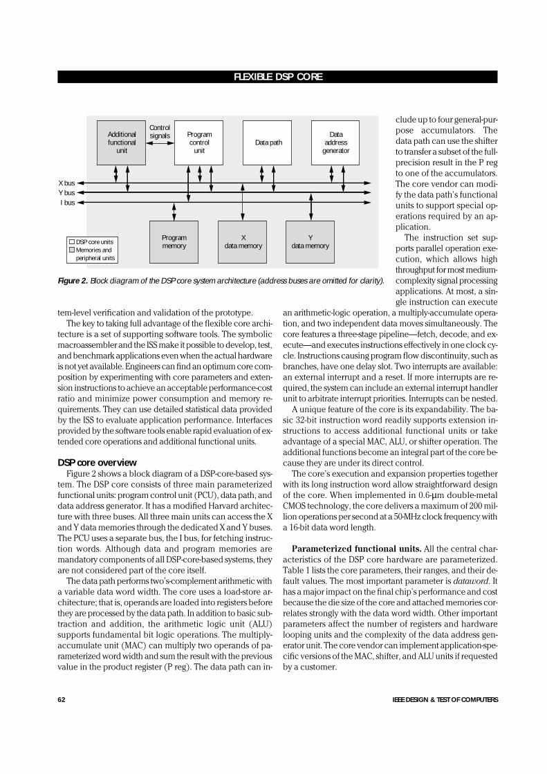
FLEXIBLE DSP CORE
62 IEEE DESIGN & TEST OF COMPUTERS
tem-level verification and validation of the prototype.
The key to taking full advantage of the flexible core archi-
tecture is a set of supporting software tools. The symbolic
macroassembler and the ISS make it possible to develop, test,
and benchmark applications even when the actual hardware
is not yet available. Engineers can find an optimum core com-
position by experimenting with core parameters and exten-
sion instructions to achieve an acceptable performance-cost
ratio and minimize power consumption and memory re-
quirements. They can use detailed statistical data provided
by the ISS to evaluate application performance. Interfaces
provided by the software tools enable rapid evaluation of ex-
tended core operations and additional functional units.
DSP core overviewFigure 2 shows a block diagram of a DSP-core-based sys-
tem. The DSP core consists of three main parameterized
functional units: program control unit (PCU), data path, and
data address generator. It has a modified Harvard architec-
ture with three buses. All three main units can access the X
and Y data memories through the dedicated X and Y buses.
The PCU uses a separate bus, the I bus, for fetching instruc-
tion words. Although data and program memories are
mandatory components of all DSP-core-based systems, they
are not considered part of the core itself.
The data path performs two’s-complement arithmetic with
a variable data word width. The core uses a load-store ar-
chitecture; that is, operands are loaded into registers before
they are processed by the data path. In addition to basic sub-
traction and addition, the arithmetic logic unit (ALU)
supports fundamental bit logic operations. The multiply-
accumulate unit (MAC) can multiply two operands of pa-
rameterized word width and sum the result with the previous
value in the product register (P reg). The data path can in-
clude up to four general-pur-
pose accumulators. The
data path can use the shifter
to transfer a subset of the full-
precision result in the P reg
to one of the accumulators.
The core vendor can modi-
fy the data path’s functional
units to support special op-
erations required by an ap-
plication.
The instruction set sup-
ports parallel operation exe-
cution, which allows high
throughput for most medium-
complexity signal processing
applications. At most, a sin-
gle instruction can execute
an arithmetic-logic operation, a multiply-accumulate opera-
tion, and two independent data moves simultaneously. The
core features a three-stage pipeline—fetch, decode, and ex-
ecute—and executes instructions effectively in one clock cy-
cle. Instructions causing program flow discontinuity, such as
branches, have one delay slot. Two interrupts are available:
an external interrupt and a reset. If more interrupts are re-
quired, the system can include an external interrupt handler
unit to arbitrate interrupt priorities. Interrupts can be nested.
A unique feature of the core is its expandability. The ba-
sic 32-bit instruction word readily supports extension in-
structions to access additional functional units or take
advantage of a special MAC, ALU, or shifter operation. The
additional functions become an integral part of the core be-
cause they are under its direct control.
The core’s execution and expansion properties together
with its long instruction word allow straightforward design
of the core. When implemented in 0.6-µm double-metal
CMOS technology, the core delivers a maximum of 200 mil-
lion operations per second at a 50-MHz clock frequency with
a 16-bit data word length.
Parameterized functional units. All the central char-
acteristics of the DSP core hardware are parameterized.
Table 1 lists the core parameters, their ranges, and their de-
fault values. The most important parameter is dataword. It
has a major impact on the final chip’s performance and cost
because the die size of the core and attached memories cor-
relates strongly with the data word width. Other important
parameters affect the number of registers and hardware
looping units and the complexity of the data address gen-
erator unit. The core vendor can implement application-spe-
cific versions of the MAC, shifter, and ALU units if requested
by a customer.
.
Dataaddress
generatorData path
Programcontrol
unit
Programmemory
Xdata memory
Ydata memory
X bus
Additionalfunctional
unit
Y busI bus
DSP core unitsMemories and peripheral units
Controlsignals
Figure 2. Block diagram of the DSP core system architecture (address buses are omitted for clarity).
.
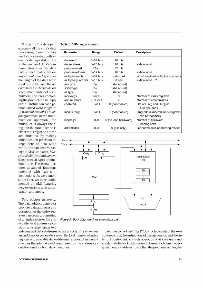
OCTOBER–DECEMBER 1997 63
Data path. The data path
executes all the core’s data
processing operations. Fig-
ure 3 shows the data path ac-
commodating a MAC unit, a
shifter, and an ALU. Various
parameters alter the data
path’s functionality. For ex-
ample, dataword specifies
the length of the data word
used by the ALU and the ac-
cumulator file. Accumulators
selects the number of accu-
mulators. The P reg contain-
ing the product of a multiply
or MAC instruction has a pa-
rameterized word length of
(2 × multiplierwidth) + multi-
plierguardbits. In the multi-
plication operation, the
multiplier is always the C
reg, but the multiplicand is
either the D reg or one of the
accumulators. By making
multiplication precision in-
dependent of data word
width, one can achieve sav-
ings in MAC unit area. Mac-
type, shiftertype, and alutype
select special types of func-
tional units. These new units
offer advanced functions
operated with extension
instructions. As we demon-
strate later, we have imple-
mented an ALU featuring
new extensions such as sat-
uration arithmetic.
Data address generator.
The data address generator
provides data addresses and
postmodifies the index reg-
isters if necessary. Consisting
of an index register file and
two identical address calcu-
lation units, it generates two
independent data addresses on each cycle. The indexregs
and addrmodes parameters select the total number of index
registers and available data-addressing modes. Dataaddress
specifies the internal word length used by the address cal-
culation units for both data memories.
Program control unit. The PCU, which consists of the exe-
cution control, the instruction address generator, and the in-
terrupt control unit, controls operation of all core units and
additional off-core functional units. It usually obtains the pro-
gram memory address from either the program counter, the
.
Table 1. DSP core parameters.
Parameter Range Default Description
dataword 8–64 bits 16 bitsdataaddress 8–23 bits 16 bits ≤ data wordprogramword 32–… 32 bitsprogramaddress 8–19 bits 16 bits ≤ data wordmultiplierwidth 8–64 bits dataword Word length of multiplier operandsmultiplierguardbits 0–16 bits 8 bits ≤ data word − 2mactype 0–… 0 (basic unit)shiftertype 0–… 0 (basic unit)alutype 0–… 0 (basic unit)indexregs 8 or 16 8 Number of index registersaccumulators 2, 3, or 4 4 Number of accumulatorsenablecd 0 or 1 0 (not enabled) Use of C reg and D reg as
ALU operandsmodifieronly 0 or 1 0 (not enabled) Only odd-numbered index registers
can be modifiersloopregs 0–8 0 (no loop hardware) Number of hardware
looping unitsaddrmodes 0–3 0 (± m only) Supported data-addressing modes
Accumulatorfile
MAC
D reg
P reg
C reg
A0A1
A3
ALU
Shifter
X busY bus
Figure 3. Block diagram of the core’s data path.
.
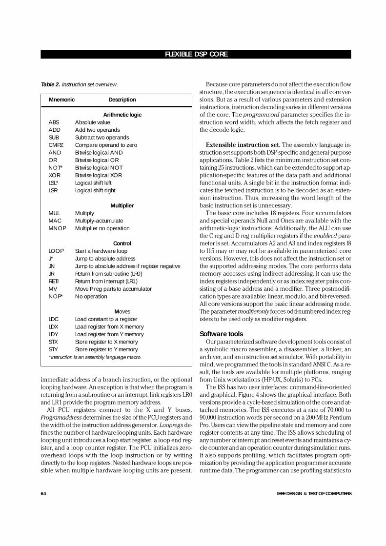
FLEXIBLE DSP CORE
64 IEEE DESIGN & TEST OF COMPUTERS
immediate address of a branch instruction, or the optional
looping hardware. An exception is that when the program is
returning from a subroutine or an interrupt, link registers LR0
and LR1 provide the program memory address.
All PCU registers connect to the X and Y buses.
Programaddress determines the size of the PCU registers and
the width of the instruction address generator. Loopregs de-
fines the number of hardware looping units. Each hardware
looping unit introduces a loop start register, a loop end reg-
ister, and a loop counter register. The PCU initializes zero-
overhead loops with the loop instruction or by writing
directly to the loop registers. Nested hardware loops are pos-
sible when multiple hardware looping units are present.
Because core parameters do not affect the execution flow
structure, the execution sequence is identical in all core ver-
sions. But as a result of various parameters and extension
instructions, instruction decoding varies in different versions
of the core. The programword parameter specifies the in-
struction word width, which affects the fetch register and
the decode logic.
Extensible instruction set. The assembly language in-
struction set supports both DSP-specific and general-purpose
applications. Table 2 lists the minimum instruction set con-
taining 25 instructions, which can be extended to support ap-
plication-specific features of the data path and additional
functional units. A single bit in the instruction format indi-
cates the fetched instruction is to be decoded as an exten-
sion instruction. Thus, increasing the word length of the
basic instruction set is unnecessary.
The basic core includes 18 registers. Four accumulators
and special operands Null and Ones are available with the
arithmetic-logic instructions. Additionally, the ALU can use
the C reg and D reg multiplier registers if the enablecd para-
meter is set. Accumulators A2 and A3 and index registers I8
to I15 may or may not be available in parameterized core
versions. However, this does not affect the instruction set or
the supported addressing modes. The core performs data
memory accesses using indirect addressing. It can use the
index registers independently or as index register pairs con-
sisting of a base address and a modifier. Three postmodifi-
cation types are available: linear, modulo, and bit-reversed.
All core versions support the basic linear addressing mode.
The parameter modifieronly forces odd-numbered index reg-
isters to be used only as modifier registers.
Software toolsOur parameterized software development tools consist of
a symbolic macro assembler, a disassembler, a linker, an
archiver, and an instruction set simulator. With portability in
mind, we programmed the tools in standard ANSI C. As a re-
sult, the tools are available for multiple platforms, ranging
from Unix workstations (HP-UX, Solaris) to PCs.
The ISS has two user interfaces: command-line-oriented
and graphical. Figure 4 shows the graphical interface. Both
versions provide a cycle-based simulation of the core and at-
tached memories. The ISS executes at a rate of 70,000 to
90,000 instruction words per second on a 200-MHz Pentium
Pro. Users can view the pipeline state and memory and core
register contents at any time. The ISS allows scheduling of
any number of interrupt and reset events and maintains a cy-
cle counter and an operation counter during simulation runs.
It also supports profiling, which facilitates program opti-
mization by providing the application programmer accurate
runtime data. The programmer can use profiling statistics to
.
Table 2. Instruction set overview.
Mnemonic Description
Arithmetic logicABS Absolute valueADD Add two operandsSUB Subtract two operandsCMPZ Compare operand to zeroAND Bitwise logical ANDOR Bitwise logical ORNOT* Bitwise logical NOTXOR Bitwise logical XORLSL* Logical shift leftLSR Logical shift right
MultiplierMUL MultiplyMAC Multiply-accumulateMNOP Multiplier no operation
ControlLOOP Start a hardware loopJ* Jump to absolute addressJN Jump to absolute address if register negativeJR Return from subroutine (LR0)RETI Return from interrupt (LR1)MV Move P reg parts to accumulatorNOP* No operation
MovesLDC Load constant to a registerLDX Load register from X memoryLDY Load register from Y memorySTX Store register to X memorySTY Store register to Y memory*Instruction is an assembly language macro.
.
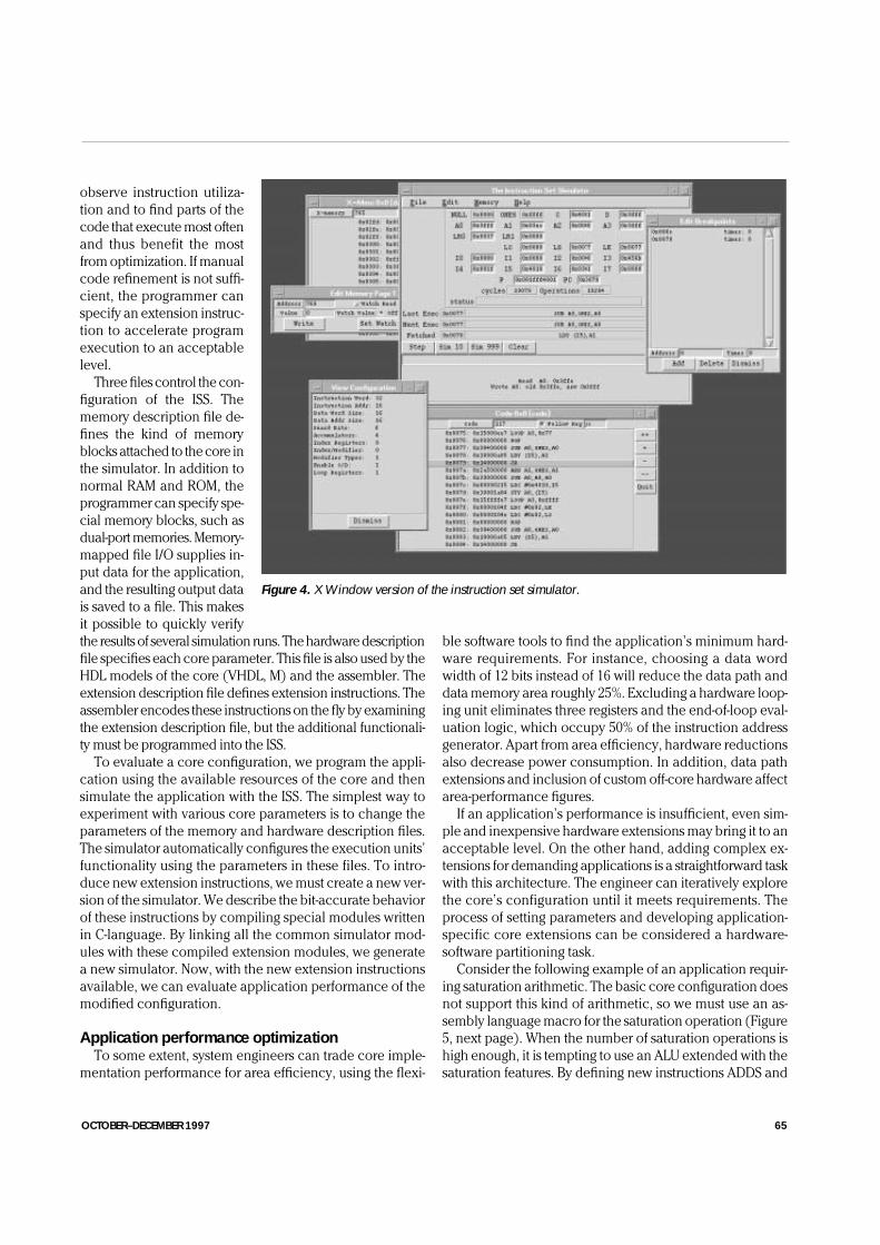
OCTOBER–DECEMBER 1997 65
observe instruction utiliza-
tion and to find parts of the
code that execute most often
and thus benefit the most
from optimization. If manual
code refinement is not suffi-
cient, the programmer can
specify an extension instruc-
tion to accelerate program
execution to an acceptable
level.
Three files control the con-
figuration of the ISS. The
memory description file de-
fines the kind of memory
blocks attached to the core in
the simulator. In addition to
normal RAM and ROM, the
programmer can specify spe-
cial memory blocks, such as
dual-port memories. Memory-
mapped file I/O supplies in-
put data for the application,
and the resulting output data
is saved to a file. This makes
it possible to quickly verify
the results of several simulation runs. The hardware description
file specifies each core parameter. This file is also used by the
HDL models of the core (VHDL, M) and the assembler. The
extension description file defines extension instructions. The
assembler encodes these instructions on the fly by examining
the extension description file, but the additional functionali-
ty must be programmed into the ISS.
To evaluate a core configuration, we program the appli-
cation using the available resources of the core and then
simulate the application with the ISS. The simplest way to
experiment with various core parameters is to change the
parameters of the memory and hardware description files.
The simulator automatically configures the execution units’
functionality using the parameters in these files. To intro-
duce new extension instructions, we must create a new ver-
sion of the simulator. We describe the bit-accurate behavior
of these instructions by compiling special modules written
in C-language. By linking all the common simulator mod-
ules with these compiled extension modules, we generate
a new simulator. Now, with the new extension instructions
available, we can evaluate application performance of the
modified configuration.
Application performance optimizationTo some extent, system engineers can trade core imple-
mentation performance for area efficiency, using the flexi-
ble software tools to find the application’s minimum hard-
ware requirements. For instance, choosing a data word
width of 12 bits instead of 16 will reduce the data path and
data memory area roughly 25%. Excluding a hardware loop-
ing unit eliminates three registers and the end-of-loop eval-
uation logic, which occupy 50% of the instruction address
generator. Apart from area efficiency, hardware reductions
also decrease power consumption. In addition, data path
extensions and inclusion of custom off-core hardware affect
area-performance figures.
If an application’s performance is insufficient, even sim-
ple and inexpensive hardware extensions may bring it to an
acceptable level. On the other hand, adding complex ex-
tensions for demanding applications is a straightforward task
with this architecture. The engineer can iteratively explore
the core’s configuration until it meets requirements. The
process of setting parameters and developing application-
specific core extensions can be considered a hardware-
software partitioning task.
Consider the following example of an application requir-
ing saturation arithmetic. The basic core configuration does
not support this kind of arithmetic, so we must use an as-
sembly language macro for the saturation operation (Figure
5, next page). When the number of saturation operations is
high enough, it is tempting to use an ALU extended with the
saturation features. By defining new instructions ADDS and
.
Figure 4. X Window version of the instruction set simulator.
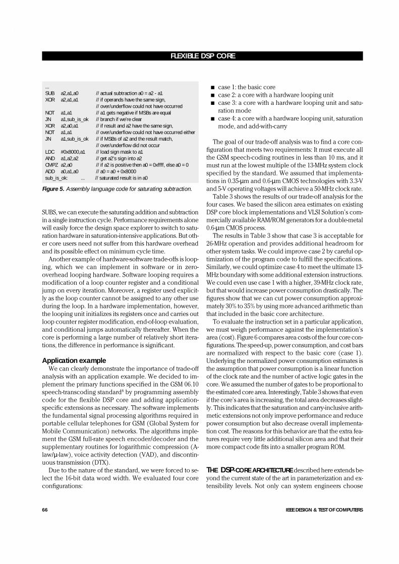
FLEXIBLE DSP CORE
66 IEEE DESIGN & TEST OF COMPUTERS
SUBS, we can execute the saturating addition and subtraction
in a single instruction cycle. Performance requirements alone
will easily force the design space explorer to switch to satu-
ration hardware in saturation-intensive applications. But oth-
er core users need not suffer from this hardware overhead
and its possible effect on minimum cycle time.
Another example of hardware-software trade-offs is loop-
ing, which we can implement in software or in zero-
overhead looping hardware. Software looping requires a
modification of a loop counter register and a conditional
jump on every iteration. Moreover, a register used explicit-
ly as the loop counter cannot be assigned to any other use
during the loop. In a hardware implementation, however,
the looping unit initializes its registers once and carries out
loop counter register modification, end-of-loop evaluation,
and conditional jumps automatically thereafter. When the
core is performing a large number of relatively short itera-
tions, the difference in performance is significant.
Application exampleWe can clearly demonstrate the importance of trade-off
analysis with an application example. We decided to im-
plement the primary functions specified in the GSM 06.10
speech-transcoding standard8 by programming assembly
code for the flexible DSP core and adding application-
specific extensions as necessary. The software implements
the fundamental signal processing algorithms required in
portable cellular telephones for GSM (Global System for
Mobile Communication) networks. The algorithms imple-
ment the GSM full-rate speech encoder/decoder and the
supplementary routines for logarithmic compression (A-
law/µ-law), voice activity detection (VAD), and discontin-
uous transmission (DTX).
Due to the nature of the standard, we were forced to se-
lect the 16-bit data word width. We evaluated four core
configurations:
■ case 1: the basic core
■ case 2: a core with a hardware looping unit
■ case 3: a core with a hardware looping unit and satu-
ration mode
■ case 4: a core with a hardware looping unit, saturation
mode, and add-with-carry
The goal of our trade-off analysis was to find a core con-
figuration that meets two requirements: It must execute all
the GSM speech-coding routines in less than 10 ms, and it
must run at the lowest multiple of the 13-MHz system clock
specified by the standard. We assumed that implementa-
tions in 0.35-µm and 0.6-µm CMOS technologies with 3.3-V
and 5-V operating voltages will achieve a 50-MHz clock rate.
Table 3 shows the results of our trade-off analysis for the
four cases. We based the silicon area estimates on existing
DSP core block implementations and VLSI Solution’s com-
mercially available RAM/ROM generators for a double-metal
0.6-µm CMOS process.
The results in Table 3 show that case 3 is acceptable for
26-MHz operation and provides additional headroom for
other system tasks. We could improve case 2 by careful op-
timization of the program code to fulfill the specifications.
Similarly, we could optimize case 4 to meet the ultimate 13-
MHz boundary with some additional extension instructions.
We could even use case 1 with a higher, 39-MHz clock rate,
but that would increase power consumption drastically. The
figures show that we can cut power consumption approxi-
mately 30% to 35% by using more advanced arithmetic than
that included in the basic core architecture.
To evaluate the instruction set in a particular application,
we must weigh performance against the implementation’s
area (cost). Figure 6 compares area costs of the four core con-
figurations. The speed-up, power consumption, and cost bars
are normalized with respect to the basic core (case 1).
Underlying the normalized power consumption estimates is
the assumption that power consumption is a linear function
of the clock rate and the number of active logic gates in the
core. We assumed the number of gates to be proportional to
the estimated core area. Interestingly, Table 3 shows that even
if the core’s area is increasing, the total area decreases slight-
ly. This indicates that the saturation and carry-inclusive arith-
metic extensions not only improve performance and reduce
power consumption but also decrease overall implementa-
tion cost. The reasons for this behavior are that the extra fea-
tures require very little additional silicon area and that their
more compact code fits into a smaller program ROM.
THE DSP-CORE ARCHITECTURE described here extends be-
yond the current state of the art in parameterization and ex-
tensibility levels. Not only can system engineers choose
.
Figure 5. Assembly language code for saturating subtraction.
...SUB a2,a1,a0 // actual subtraction a0 = a2 - a1XOR a2,a1,a1 // if operands have the same sign,
// over/underflow could not have occurredNOT a1,a1 // a1 gets negative if MSBs are equalJN a1,sub_is_ok // branch if we’re clearXOR a2,a0,a1 // if result and a2 have the same sign,NOT a1,a1 // over/underflow could not have occurred eitherJN a1,sub_is_ok // if MSBs of a2 and the result match,
// over/underflow did not occurLDC #0x8000,a1 // load sign mask to a1AND a1,a2,a2 // get a2’s sign into a2CMPZ a2,a0 // if a2 is positive then a0 = 0xffff, else a0 = 0ADD a0,a1,a0 // a0 = a0 + 0x8000sub_is_ok: ... // saturated result is in a0

OCTOBER–DECEMBER 1997 67
peripherals and the basic
data word width. They can
also configure more ad-
vanced parameters such as
addressing modes, hardware
looping, and various address
and data word widths within
the core to suit application re-
quirements. With the exten-
sion instructions, they can
fine-tune existing operations,
add new core operations, or
use custom logic much like a
coprocessor controlled di-
rectly by the core control
unit. We know of no other ex-
isting DSP cores that accom-
modate such a flexible set of
extension mechanisms.
As the speech coding
example shows, the architec-
ture is sufficient for executing
signal processing algorithms
of at least medium complexi-
ty. However, it is not sufficient
for the most complex signal
processing algorithms, since
its parallelism cannot always
be used efficiently. Some DSP
programmers may consider
the jump condition set too limited, and the implementation
of extended-precision arithmetic is not straightforward. The
commercial partner of this project addressed these limitations
in a second-generation core called VS-DSP.9 While this core
retains the original’s level of parameterization and extensibil-
ity, its more orthogonal register set and larger selection of
branch conditions make programming easier.
The software development tools supporting the parame-
ter space and extension attachment are essential to fine-
tuning the core architecture for a specific application. One
can regard the parameterized core as a broad DSP-core fam-
ily, rather than a single core. The implemented software tools
adjust successfully to the family’s varying features. We also
revised the tools to support the VS-DSP instruction set and ar-
chitecture, proving the flexibility of the software tools.
The elastic DSP core and supporting software tools enable
exploration of the application design space. Developers can
find the most appropriate division between hardware-
supported and software-coded operations for a particular ap-
plication by experimenting in software before proceeding to
a hardware implementation. In addition to optimizing perfor-
mance, they can balance the use of data and program mem-
ory and hardware logic to reach the most economical real-
ization of the application algorithm. Also, an extension of the
.
Table 3. GSM application performance. All routines must execute in less than 10 ms.
Case 1 Case 2 Case 3 Case 4
Worst-case runtime by section (cycles)GSM 06.10 full-rate transcoder
Encoder 193,487 172,208 126,643 109,755Decoder 68,654 63,009 18,967 18,967G.711 (A-law/µ-law) 26,000 25,298 25,298 25,298
GSM 06.31 DTX handler 10,000 9,788 9,788 9,788GSM 06.32 VAD 21,700 21,380 21,380 20,480Total cycle count 319,841 291,683 202,076 184,258Normalized cycle count (speed-up) 1.00 1.10 1.58 1.74Lowest feasible clock frequency 32.0 MHz 29.2 MHz 20.3 MHz 18.5 MHz% of cycle budget in use @ 50 MHz 63% 58% 40% 36%
Memory usage (words × bits)Program ROM 4,002 × 32 3,908 × 32 3,837 × 32 3,807 × 32X RAM 1,182 × 16 1,182 × 16 1,182 × 16 1,182 × 16Y RAM 616 × 16 616 × 16 616 × 16 616 × 16Y ROM 441 × 16 441 × 16 441 × 16 441 × 16
Estimated area in 0.6-µm CMOS (mm2)Core 3.50 3.80 3.82 3.85Program ROM 4.25 4.15 4.10 4.05Data memory 9.20 9.20 9.20 9.20Total area 16.95 17.15 17.12 17.10Normalized total area (cost) 1.000 1.012 1.010 1.009
1.00
Application speed-up
0.98
0.69
0.63
1.000.920.640.58
1.001.101.581.74
Estimated power consumption (core area/number of cycles)
Cost of speed-up (total area/number of cycles)
Case 1Case 2Case 3Case 4
Figure 6. Normalized comparisons of the four evaluated cases.
FLEXIBLE DSP CORE
68 IEEE DESIGN & TEST OF COMPUTERS
DSP core’s functional units can replace part of the surround-
ing logic circuitry of a more conventional ASIC implementa-
tion. The extension instructions become an integral part of the
DSP core. Thus, an application software developer can effort-
lessly comprehend how the additional hardware synchronizes
and interfaces with the core’s execution flow.
AcknowledgmentsThe DSP-core development was a joint project of VLSI Solution
and Tampere University of Technology, both in Tampere, Finland.
VLSI Solution and the Technology Development Center TEKES
funded the project.
We thank Juha Roström of VLSI Solution for providing us infor-
mation about the speech-coding algorithm implementation.
References1. P.G. Paulin et al., “Trends in Embedded Systems Technology,”
in Hardware/Software Co-Design, Kluwer Academic, Norwell,
Mass., 1996, pp. 311-337.
2. A.J.P Bogers et al., “The ABC Chip: Single Chip DECT Baseband
Controller Based on EPICS DSP Core,” Proc. Int’l Conf. Signal
Processing Applications and Technology, 1996, pp. 299-302.
3. C. Liem et al., “System-on-a-Chip Cosimulation and Compila-
tion,” IEEE Design & Test of Computers, Vol. 14, No. 2, Apr.-June
1997, pp. 16-25.
4. P.D. Lapsley, J.C. Bier, and A. Shoham, Buyer’s Guide to DSP
Processors, Berkeley Design Technology Inc., Berkeley, Calif.,
1995.
5. H. Yagi and R.E. Owen, “Architectural Considerations in a Con-
figurable DSP Core for Consumer Electronics,” VLSI Signal Pro-
cessing, VIII, IEEE Press, Piscataway, N.J., 1995, pp. 70-81.
6. R. Woudsma et al., “EPICS—A Flexible Approach to Embed-
ded DSP Cores,” Proc. Int’l Conf. Signal Processing Applications
and Technology, 1994, pp. 506-511.
7. J. Nurmi, “Portability Methods in Parameterized DSP Module
Generators,” VLSI Signal Processing, VI, IEEE Press, Piscataway,
N.J., 1993, pp. 260-268.
8. Recommendation GSM 06.10, GSM Full Rate Speech Transcod-
ing, European Telecommunications Standards Institute (ETSI),
Sophia Antipolis, France, 1992.
9. J. Nurmi and J. Takala, “A New Generation of Parameterized
and Extensible DSP Cores,” Proc. IEEE Workshop on Signal Pro-
cessing Systems, Leicester, UK, 1997.
Mika Kuulusa is a research scientist in the
Signal Processing Laboratory at Tampere Uni-
versity of Technology, Finland. He is working
toward the doctor of technology degree. His
current research activities focus on hardware-
software codesign of systems based on DSP
cores. Other areas of interest include embed-
ded-software compilation, logic synthesis, VLSI implementation,
and IC design. Kuulusa received his MSc degree in information
technology from Tampere University of Technology.
Jari Nurmi is the vice president of VLSI So-
lution Oy in Tampere, Finland. His research
interests include DSP cores and application-
specific DSP architectures and their VLSI im-
plementation. Previously, he worked in
Tampere University of Technology’s Signal
Processing Laboratory as leader of the DSP
and Computer Hardware Group. Nurmi received his MSc and li-
centiate of technology degrees in electrical engineering and his
doctor of technology degree in information technology from Tam-
pere University of Technology. He is a member of the IEEE.
Janne Takala is an IC designer at VLSI Solu-
tion Oy, where he is involved in developing
and implementing DSP core architectures. He
is also working toward the MSc degree at Tam-
pere University of Technology.
Pasi Ojala is a software engineer at VLSI So-
lution Oy. Previously, he worked as a research
assistant in the Signal Processing Laboratory
of Tampere University of Technology. His re-
search interests range from digital system de-
sign and low-level programming to writing
application software for end users. Ojala re-
ceived his MSc degree in information technology from Tampere
University of Technology.
Henrik Herranen is a software developer at
VLSI Solution Oy. Previously, he worked as a
research assistant in the Signal Processing
Laboratory of Tampere University of Tech-
nology, where he is also working toward his
MSc degree.
Address questions or comments about this article to Mika Ku-
ulusa, Signal Processing Laboratory, Tampere University of Tech-
nology, PO Box 553 (Hermiankatu 12), 33101 Tampere, Finland;
.

PUBLICATION 3
M. Kuulusa, T. Parkkinen, and J. Niittylahti, “MPEG-1 layer II audio decoder
implementation for a parameterized DSP core,” in Proc. Int. Conference on Signal
Processing Applications and Technology, Orlando, FL, U.S.A., Nov. 1–4 1999 (CD-ROM).
Copyright c©1999 Miller Freeman, Inc. Reprinted, with permission, from the proceedings
of ICSPAT’99.

Abstract
A compact, fixed-point DSP core can beutilized to realize an MPEG-1 Layer II audiodecoder. The firmware for the decodingalgorithm was implemented by transforminga floating-point C-language source code intoan efficient assembly language code for theDSP. This paper describes our systematicdesign approach and reviews the programcode behavior in light of detailed statisticalprofiling information.
1. Introduction
MPEG digital audio coding is the audiocompression standard utilized in manymodern applications, such as digital audiobroadcasting (DAB) and digital versatile disc(DVD) players. Since the consumer productstypically require only the decoding of thecompressed audio stream, a successfulimplementation of the audio decoderbecomes imperative. Often the most suitableway to realize the audio decoder is to use aprogrammable DSP jointly with an optimizedassembly language module to perform all thenecessary decoding functions.
Although an audio decoder implementationutilizing floating-point arithmetic typicallyresults in better quality of the reproducedaudio, the cost of the floating-point DSPs isclearly prohibitive. Therefore, fixed-pointDSPs are utilized to achieve a more cost-effective solution. In our approach, we havetaken a flexible fixed-point DSP core as the
target platform for our MPEG-1 Layer IIaudio decoder.
The paper begins with a brief overview to theMPEG audio coding standards. A systemarchitecture incorporating an MPEG audiodecoder chip is described and thedevelopment of the audio decoder firmwareis presented. The run-time characteristics ofthe audio decoder implementation are studiedin detail. Finally, the conclusions are drawn.
2. MPEG Audio Coding
2.1 Overview
MPEG audio compression algorithms areinternational standards for digitalcompression of high-fidelity audio. TheMPEG audio-coding standard offers audioreproduction which is equivalent to CDquality (16-bit PCM). MPEG-1 audio covers32, 44.1, and 48 kHz sampling rates forbitrates ranging from 32 to 448 kbit/s [1]. TheMPEG-1 audio supports four modes: mono,stereo, joint-stereo and dual-channel. Thestandard defines three Layers whichfundamentally differ in their compressionratios with respect to the quality of thereproduced audio. For transparent quality,Layer I, Layer II, and Layer III require 384,192, and 128 kbit/s bitrates, respectively. TheMPEG-2 standard introduces several newfeatures, such as an extension formultichannel audio and support for lowersampling frequencies [2]. A morecomprehensive description of the MPEGaudio compression can be found in [3],[4].
MPEG-1 Layer II Audio Decoder Implementation for aParameterized DSP Core
Mika Kuulusa, Teemu Parkkinen and Jarkko NiittylahtiSignal Processing Laboratory, Tampere University of Technology
P.O. Box 553 (Hermiankatu 12), Tampere, Finland
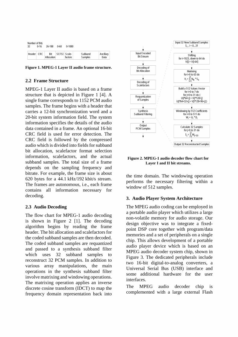
2.2 Frame Structure
MPEG-1 Layer II audio is based on a framestructure that is depicted in Figure 1 [4]. Asingle frame corresponds to 1152 PCM audiosamples. The frame begins with a header thatcarries a 12-bit synchronization word and a20-bit system information field. The systeminformation specifies the details of the audiodata contained in a frame. An optional 16-bitCRC field is used for error detection. TheCRC field is followed by the compressedaudio which is divided into fields for subbandbit allocation, scalefactor format selectioninformation, scalefactors, and the actualsubband samples. The total size of a framedepends on the sampling frequency andbitrate. For example, the frame size is about620 bytes for a 44.1 kHz/192 kbit/s stream.The frames are autonomous, i.e., each framecontains all information necessary fordecoding.
2.3 Audio Decoding
The flow chart for MPEG-1 audio decodingis shown in Figure 2 [1]. The decodingalgorithm begins by reading the frameheader. The bit allocation and scalefactors forthe coded subband samples are then decoded.The coded subband samples are requantizedand passed to a synthesis subband filterwhich uses 32 subband samples toreconstruct 32 PCM samples. In addition tovarious array manipulations, the mainoperations in the synthesis subband filterinvolve matrixing and windowing operations.The matrixing operation applies an inversediscrete cosine transform (IDCT) to map thefrequency domain representation back into
the time domain. The windowing operationperforms the necessary filtering within awindow of 512 samples.
3. Audio Player System Architecture
The MPEG audio coding can be employed ina portable audio player which utilizes a largenon-volatile memory for audio storage. Ourdesign objective was to integrate a fixed-point DSP core together with program/datamemories and a set of peripherals on a singlechip. This allows development of a portableaudio player device which is based on anMPEG audio decoder system chip, shown inFigure 3. The dedicated peripherals includetwo 16-bit digital-to-analog converters, aUniversal Serial Bus (USB) interface andsome additional hardware for the userinterfaces.
The MPEG audio decoder chip iscomplemented with a large external Flash
Figure 1. MPEG-1 Layer II audio frame structure.
Header CRC BitAllocation
SCFSI Scale-factors
SubbandSamples
AncillaryData
Number of Bits32 0-16 26-188 0-60 0-1080
Figure 2. MPEG-1 audio decoder flow chart forLayer I and II bit streams.
Input EncodedBit Stream
Decoding ofBit Allocation
Decoding ofScalefactors
Requantizationof Samples
SynthesisSubband Filtering
OutputPCM Samples
Input 32 New Subband SamplesSi , i = 0...31
Shiftingfor i=1023, down to 64 do
V[i] = V[i-64]
Matrixingfor i=0 to 63 do
Vi = Σ Nik * Sk
Build a 512 Values Vectorfor i=0 to 7 do
for j=0 to 31 do {U[i*64+j] = V[i*128+j]
U[i*64+32+j] = V[i*128+96+j] }
Windowing by 512 Coefficientsfor i=0 to 511 do
Wi = Ui * Di
Calculate 32 Samplesfor j=0 to 31 do
Sj = Σ Wj+32i
Output 32 Reconstructed Samples
31
k=0
15
i=0

memory. A 96 MB Flash memory can holdapproximately 70 minutes of 192 kbit/s audiostreams. Moreover, the external memorycontains the program code and various dataarrays which are downloaded into the on-chipmemories during the system initialization.
The DSP core is based on a modified Harvardarchitecture with a separate program memoryand two data memories [5]. The executionpipeline contains three stages whicheffectively fetch, decode and execute 32-bitinstruction words. The DSP core has aflexible architecture that allows a number ofparameters to be changed to suit the specificneeds of the application at hand [6]. Theadjustable data word length allows us toincrease the dynamic range of thecalculations in case the audio decoder wouldnot have satisfactory audio quality. However,a 16-bit data word width was selected for ourinitial implementation. In this configuration,the processor datapath contains eight 16-bitregisters which can also be used as four 40-bitaccumulators. Eight data address registerscan be employed to realize indirect datamemory accesses together with various post-modification operations. Moreover, theprocessor supports zero-overhead programlooping.
4. Audio Decoder Implementation
Several C-language audio decoders wereextensively studied to facilitate theimplementation in an assembly language.Based on various experiments, a floating-point C-source code was selected for furtherrefinement. A systematic approach was takento transform this floating-point version intoan efficient assembly language program.First, the floating-point C-language decoderwas modified to employ 16-bit arithmeticoperations and data values instead of single-precision floating-point. The fixed-valueddata arrays employed in the matrixing andwindowing operations were scaled andtruncated to fixed-point representationswhich provided satisfactory audio quality.However, certain operations had to be carriedout with 32×16-bit multiply-accumulate(MAC) operations. These operations wereperformed by using an assembly macro thatexecutes the multiplication with fourinstructions. An alternative way to realizethese MACs would be by extending thelength of the data word. However, this wasnot found necessary since the criteria for thedecoder performance and audio quality werefulfilled, thus the additional cost was notjustified. The 32-point IDCT operations in
Figure 3. Block diagram of the MPEG audio decoder chip with an external Flash memory.
96 MBFlash Memory
X DataMemory
DisplayController
KeyboardInterface
Misc.Peripherals
USBInterface
2 x 16-bitDAC
Y DataMemory
DSP Core
ProgramMemory
External Bus Interface
MPEG Audio Decoder
the synthesis subband filter were effectivelyrealized with Lee’s fast algorithm [7]. Thefast algorithm reduces the original 2048multiply-accumulate operations into 80multiplications and 209 additions.
The optimized fixed-point C-languageprogram served as a bit-exact functionalrepresentation for our implementation thatwas hand-coded in assembly language for thetarget DSP. Since all the calculations wereperformed with 16-bit arithmetic operations,the modified C-language program allowed astraightforward conversion process from C-language to DSP assembly code. Theassembly language implementation of theMPEG-1 Layer II audio decoder has aprogram size of 2272 words. Data memoryusage is 12325 words, of which 74% is usedto accommodate various fixed-valued datatables needed in the audio frame decodingand the synthesis subband filtering.
5. Audio Decoder Performance
The audio decoder implementation wasevaluated with different types of audiomaterial that were encoded into audiostreams for bitrates ranging from 64 kbit/s to320 kbit/s. The firmware was simulated witha cycle-accurate instruction-set simulator ofthe DSP core. Table 1 shows the results for44.1 kHz stereo streams.
For these streams, it was assumed that a totalof 39 frames has to be decoded in one second.In order to get a worst-case estimate, several5 second streams were decoded and thelongest run-time for one frame wasmultiplied by 39. The variation in the clockcycles per frame is not very large, typicallyless than 3% of the worst-case run-times.Depending on the bitrate and samplingfrequency of the audio, real-time decodingcan be achieved at relatively low processorclock frequencies. For 44.1 kHz stereo audioat bitrates less than 192 kbit/s, a clock
frequency of 25 MHz is sufficient providingadditional capacity for other system tasks.
Table 2 shows the percentages and thenumber of clock cycles for the main functionsin the audio decoder.
As expected, the matrixing and windowingoperations in the synthesis subband filteringdominate, consuming roughly 78% of thedecoding time. The requantization of samplestakes 20% and the remaining 2% of the clockcycles is spent in input/output operations andfunctions that are performed only once perframe. By investigating Table 2, the decoder
Table 1: Worst-case decoder run-times for onesecond of 44.1 kHz stereo audio.
Bitrate(kbit/s)
Decoder Run-Time(clock cycles)
64 21 225 000
128 23 435 000
192 24 575 000
256 25 688 000
320 26 156 000
Table 2: Processing requirements for the mainaudio decoder functions.
MPEG-1 Layer IIDecoder Function
%Clock
Cycles*
Decoding of Bit AllocationDecoding of Scalefactors
1.4 350 000
Requantization of Samples 19.9 4 975 000
Matrixing 42.9 10 725 000
Windowing 35.0 8 750 000
Input/Output 0.7 175 000
Other 0.1 25 000
All 100 25 000 000
* Decoding time of 25 000 000 clock cycles assumed.

functions that benefit most from furtheroptimization are clearly the matrixing andwindowing operations. For example, thewindowing operation has a program kernelconsisting of blocks of five instructions. Thiskernel contributes roughly 30% of the totalrun-time of the decoder. If a 24-bit data wordwere used, it would be possible to realize thekernel with only two instructions.Effectively, this modification would reduce24%, or about 6 million clock cycles, fromthe decoding time. On the other hand, thequality of the reproduced audio could beimproved by employing block floating-pointarithmetics in the synthesis subband filter [8].However, block floating-point arithmeticswould increase the number of clock cyclesneeded in the audio decoding.
6. Conclusions
An MPEG-1 Layer II audio decoder wassuccessfully realized for a fixed-point DSPcore with a 16-bit data word. A 25 MHzprocessor clock frequency was foundsufficient to accomplish decoding of44.1 kHz stereo audio streams at a 192 kbit/sbitrate. The audio decoder implementationprovides audio reproduction with goodperceptual quality. The developed firmwarecan be utilized in an integrated MPEG audiodecoder chip which offers a cost-effectiveaudio decoding solution for a wide range ofconsumer electronics applications.
7. Acknowledgments
The research work has been co-funded by theNational Technology Agency of Finland andseveral companies from the Finnish industry.The support received from VLSI Solution Oyis gratefully acknowledged.
References
[1] ISO/IEC 11172-3, “InformationTechnology - Coding of Moving Picturesand Associated Audio for Digital StorageMedia at up to about 1.5 Mbit/s - Part 3:Audio”, Standard, InternationalOrganization for Standardization,Geneva, Switzerland, Mar. 1993.
[2] ISO/IEC 13818-3, “InformationTechnology - Generic Coding of MovingPictures and Associated Audio: Audio,”Standard, International Organization forStandardization, Geneva, Switzerland,Nov. 1994.
[3] P. Noll, “MPEG Digital Audio Coding,”IEEE Signal Processing Magazine, vol.14, no. 5, pp. 59-81, Sep. 1997.
[4] D. Pan, “A Tutorial on MPEG/AudioCompression,”IEEE Multimedia, vol. 2no. 2, pp. 60-74, Summer 1995.
[5] VLSI Solution Oy,VS_DSP SpecificationDocument, rev. 0.8, Nov. 1997.
[6] J. Nurmi and J. Takala, “A NewGeneration of Parameterized andExtensible DSP Cores,” inProc. IEEEWorkshop on Signal Processing Systems,Leicester, United Kingdom, Nov. 1997,pp. 320-329.
[7] K. Konstantinides, “Fast SubbandFiltering in MPEG Audio Coding,”IEEESignal Processing Letters, vol.1, no. 2,pp. 26-28, Feb. 1994.
[8] R. Ralev and P. Bauer, “ImplementationOptions for Block Floating Point DigitalFilters,” in Proc. IEEE Int. Conf. onAcoustics, Speech and Signal Processing,Munich, Germany, Apr. 1997, pp. 2197-2200.

PUBLICATION 4
M. Kuulusa, J. Nurmi, and J. Niittylahti, “A parallel program memory architecture for a
DSP,” in Proc. Int. Symposium on Integrated Circuits, Devices & Systems, Singapore, Sep.
10–12 1999, pp. 475–479.
Copyright c©1999 Nanyang Technological University, Singapore. Reprinted, with
permission, from the proceedings of ISIC’99.


1. INTRODUCTION
Most embedded systems contain a non-volatilememory for permanent storage of the applicationfirmware that is executed by programmable processors.Reprogrammability of this memory has become one ofthe key requirements because it allows firmwareupdates later in the design cycle or even on the field.From the current non-volatile memory technologies,low-cost high-capacity flash memory devices havegained widespread acceptance in DSP-based embeddedsystems, such as cellular phones. Because flashmemory devices are inherently slow, currentlyproviding read access times in the 40-70 ns range, theprogram execution cannot be carried out directly fromthe flash memory. During the system initialization, theprogram code is copied entirely, or partly, to an on-chipprogram memory to enable rapid program execution.Moreover, in low-power applications the access timesto on-chip SRAM memories tend to increasesignificantly when lower supply voltages are employed.
If the program code could be executed directlyfrom the non-volatile memory, meaningful cost-savingscould be realized since the separate fast programmemory could be eliminated from the system. Inaddition, a low-power program memory could berealized if there were some means to compensate theslow read access time.
The effective program memory bandwidth,however, can be increased if the read accesses areperformed in parallel, i.e., several instruction words areread simultaneously. In this paper, a parallel programmemory architecture for a DSP core is presented. Toallow reasonable evaluation of the parallel memoryarchitecture, a behavioral-level hardware model of acommercial DSP core was used in the development.Two applications were used to analyze the suitability of
the memory architecture and the effect on the programexecution with this particular DSP was studied.
2. PROGRAM EXECUTION IN THE DSP
A fixed-point DSP core, designated VS_DSP[1], was chosen as the target processor of a parallelprogram memory architecture. Program execution isbased on a shallow three-stage pipeline comprising ofinstruction fetch, decode and execute phases. Allinstructions effectively execute in one clock cycle. TheDSP core incorporates three main blocks: a programcontrol unit (PCU), datapath and data address generator(DAG). A detailed description of the DSP core can befound from [2,3], reference [4] has a presentation of thefirst generation DSP core.
The operation of the PCU is illustrated inFigure 1. Depending on the current processor state andthe decoded instruction, the next instruction fetchaddress may come from a variety of sources:
• incremented program counter (PC)• target address of a branching instruction• subroutine or interrupt return address registers• loop start address register, and• interrupt or reset vector addresses.
Typically, the next address is fetched from theincremented PC to carry out sequential execution of theprogram code. Discontinuity in the sequential programflow is caused by branching/return instructions, or itmay result from an activity of the looping hardware andthe interrupt controller. Target addresses for conditionaland unconditional branching instructions are embeddedinto the 32-bit instruction word. Other possibleaddresses are either fixed values or they are fetchedfrom dedicated registers.
A PARALLEL PROGRAM MEMORY ARCHITECTURE FOR A DSP
Mika Kuulusa, Jari Nurmi and Jarkko Niittylahti
Signal Processing Laboratory, Tampere University of Technology,P.O. Box 553 (Hermiankatu 12), FIN-33101 Tampere, Finland
Tel. +358 3 3652111, Fax +358 3 3653095,E-mail: [email protected]
Abstract : This paper describes an approach where a DSP core is coupled with a parallel program memory architectureto allow rapid program execution from a number of slow memory banks. The slow read access time to the memory banksmay be due to lowered supply voltages or it can be a property of the memory technology itself. Thus, the approach hastwo benefits: 1) it allows program execution directly from a non-volatile memory to reduce the system cost, and 2) lowersupply voltages can be employed in low-power applications. The suitability of the memory architecture is evaluated withassembly language implementations of an MPEG audio decoder and a GSM speech codec. The results show that thespeed-up of a highly sequential program code is directly proportional to the number of memories, whereas in a morecomplex application only a 2x speed-up is achievable.
475

In the DSP core, a non-sequential program memoryaccess resulting from a jump instruction (i.e., abranching or return instruction) is performed by usingdelayed branching method, i.e., the instructionfollowing a jump instruction is always executed. Theexecution overhead arising from this approach isacceptable since in typical applications, 80-90% of thedelay slots can be fitted with a useful instruction. Forexample, the delay slot can be utilized to store asubroutine return address or to pass one of thesubroutine arguments.
When the pipelined execution flow isconsidered, another problematic issue is the operationduring interrupts. As soon as an interrupt is detected, afetch from the fixed interrupt vector address is issued.Now, the pipeline has two instructions in the decodeand execute stages. The PCU selectively picks out thecorrect interrupt return address from the followingoptions:
• address of the instruction (in decode)• jump instruction target address (in execute), or• loop start address.
If the first option is chosen, the instruction in thedecode stage has to be canceled. However, thisinstruction is executed normally, if either 1) theinstruction in the execute is a jump to be taken, or, 2)the instruction was fetched from loop end address and anew iteration should be taken.
3. PARALLEL PROGRAM MEMORYARCHITECTURE
A general block diagram of a parallel memoryarchitecture is depicted in Figure 2. The memoryarchitecture comprises of an address generator unit, apermutation network, and a total of N memory banks[5]. Depending on the selected access format, theaddress generation unit provides a memory address foreach of the memory banks. An access format can becomprehended as a template that is positioned on a two-dimensional representation of the entire memory space.Common access formats are a row, a rectangle and a
diagonal line, for example. Permutation network isrequired to rearrange data values so that the input oroutput can be manipulated in a correct order.
3.1. Parallel Program Memory
A suitable architecture for a parallel programmemory can be derived from the general architectureby considering the pipelined operation of the DSP core.Such a memory architecture is depicted in Figure 3.
The PCU operation is modified to contain allthe necessary functions of the address generator. Apipelined read access to a parallel memory with Nmemory banks is specified to last a total of N clockcycles. Therefore, it is possible to issue N individualaddresses to the memory banks so that only a non-sequential memory access will result in a memoryaccess penalty. In processor clock cycles, this penalty isN-1 clock cycles. The permutation network can bereplaced with an N-to-1 multiplexer which is controlledby the stream of absolute program memory addressesthat are sequenced through N-1 shift registers.Moreover, loop start addresses needed in theinitialization of the hardware looping are acquired fromone of the shift registers.
3.2. Program Code Mapping
The program code is interleaved to the memorybanks [6]. Let us consider a value of N which is a power
of two (N = 2M). Instruction words are interleaved tothe memory banks with the following mapping:
Mi(addr) = P(addr + i mod N) (1)
where Mi(x) are the contents of a memory location x inthe memory bank i, P(y) is the instruction word in theabsolute program memory address y, i = [0, N-1],addr = [0, program_address_space-1]. By using thismapping, a parallel read access to the address K resultsin an instruction block containing the following Ninstruction words:
Fig. 1. Possible sources for the next program address inthe DSP core.
Program Control Unit
Instruction Data Bus
Instruction Address Bus
SubroutineReturn
Address(LR0)
LoopStart
Address(LS)
BranchingTarget
Address
InterruptVector0x0008
ResetVector0x0000
Decode
InterruptReturn
Address(LR1)
Next Instruction Address
ProgramCounter
Increment
Status RegistersInterrupt ControlHardware Looping
Mux
Fig. 2. General parallel memory architecture.
MemoryBank
0
MemoryBank
1
MemoryBank
2. . .
MemoryBankN-1
Address Generator
Permutation Network
Access Format
Read/Write Control
Data Output/Input
Memory Address
476

[ M0(K) M1(K) M2(K) ... MN-1(K) ] =[ P(A) P(A+1) P(A+2) ... P(A+N-1) ] (2)
where A=K*N. In other words, the result is the Nsequential instruction words starting from absolute pro-gram memory address A. In the case all memoryaccesses could be aligned to N word boundaries, a sin-gle address could be issued. But since the PCU canselectively issue new addresses to the memory banks,the pipelined program memory access is straightforwardto implement. Conceptually, the single cycle instructionfetch stage is stretched to cover N processor clockcycles.
An interesting option in the presented memoryarchitecture is that there is a straightforward way tosupport memory architectures where N is not a power oftwo. The use of such a program memory only requires afew additional steps in the program code assembly, anda minor change to the generation of the sequentialprogram memory addresses in the PCU.
4. IMPLICATIONS ON THE PROGRAMMEMORY ADDRESSING
4.1. Branching/Return Instructions
From the program execution point of view, theobjective was to make the branching/return instructionsfunction exactly in the same manner as in the singlememory case. Therefore, the execution of theinstruction in the delay slot remains the same, but due tothe non-sequential memory access latency, N-1instructions after the delay slot have to be cancelled.
4.2. Interrupt Operation
Interrupt operation in the parallel memoryarchitecture is mainly constrained by the hardwarelooping operation because the pipeline may containinstructions from a new loop iteration. To enable correctoperation, the interrupt return address has to be
determined sequentially by examining the instructionsin the pipeline, in a similar way as described in Section2. This leads to the worst-case interrupt latency of (1 +2N) clock cycles, whereas the minimum latency is(N+2). Interrupt latency is defined as the time neededfrom the interrupt detection to the execution of the firstinstruction of the interrupt service routine. Clearly, theactual interrupt overhead in a certain applicationdepends on the rate at which the interrupts occur. Theoverhead is not an issue when the interrupt rate isrelatively low.
4.3. Hardware Looping
In order to avoid complications in the hardwarelooping, a loop body, i.e., the program code in the loops,must always contain a number of instructions which is amultiple of N. However, if the number of iterations is aconstant value known at the program compile-time, thisrestriction can be avoided with loop unrolling. In loopunrolling, a new loop body is constructed by replacingthe original code with several copies of the loop body,and adjusting the number of loop iterationsappropriately. In this way the resulting loop body is amultiple of N, and the overhead arising from the parallelmemory architecture is minimized. Unfortunately, loopunrolling can be employed only to certain extent, thus insome cases a loop body must be padded with no-operations resulting in a very undesirable overhead.
5. EXPERIMENTAL RESULTS OF THEMEMORY ARCHITECTURE
Two different applications were used toevaluate the performance of the parallel memoryarchitecture: GSM half rate speech codec and MPEG-1Layer II audio decoder [7][8]. The GSM half ratespeech encoder compresses a 13-bit speech signalsampled at 8 kHz into a 5.6 kbit/s information stream.Both the GSM half rate encoder and decoder were runsequentially during the experiments. MPEG-1 Layer IIdecoder was used to reconstruct 16-bit audio samples(44.1 kHz, stereo) from a 128 kbit/s compressed audiodata stream.
The experiments were carried out by runningan extensive program trace from both of theapplications by using an instruction-set simulator of theDSP core. The simulator allows a cycle-accuratesimulation of the applications and generates profilinginformation of the dynamic behavior of the programcode. The program traces were analyzed withautomated scripts that calculate the number of jumpinstructions and the number of no-operation instructionsrequired to adjust the hardware looping sections. Loopunrolling was not applied in the applications. Theapplication performance was calculated for memoryconfigurations that have 1 to 8 memory banks.
The results from the GSM half rate test areshown in Figure 4. Three curves illustrate theperformance in cases with no jump/looping overhead
Fig. 3. Parallel program memory architecture suitable forpipelined memory accesses (N=4).
MemoryBank
0
MemoryBank
1
MemoryBank
2
MemoryBank
3
Mux
ProgramControl
Unit
32 32 32 32
32
14 14 14 14
Instruction Address Buses
Instruction Data Bus
16
D
D
D
2
477
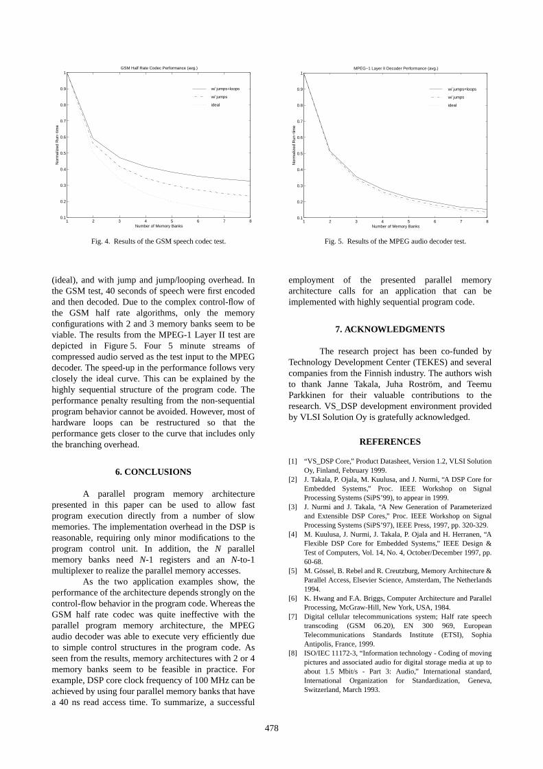
(ideal), and with jump and jump/looping overhead. Inthe GSM test, 40 seconds of speech were first encodedand then decoded. Due to the complex control-flow ofthe GSM half rate algorithms, only the memoryconfigurations with 2 and 3 memory banks seem to beviable. The results from the MPEG-1 Layer II test aredepicted in Figure 5. Four 5 minute streams ofcompressed audio served as the test input to the MPEGdecoder. The speed-up in the performance follows veryclosely the ideal curve. This can be explained by thehighly sequential structure of the program code. Theperformance penalty resulting from the non-sequentialprogram behavior cannot be avoided. However, most ofhardware loops can be restructured so that theperformance gets closer to the curve that includes onlythe branching overhead.
6. CONCLUSIONS
A parallel program memory architecturepresented in this paper can be used to allow fastprogram execution directly from a number of slowmemories. The implementation overhead in the DSP isreasonable, requiring only minor modifications to theprogram control unit. In addition, the N parallelmemory banks need N-1 registers and an N-to-1multiplexer to realize the parallel memory accesses.
As the two application examples show, theperformance of the architecture depends strongly on thecontrol-flow behavior in the program code. Whereas theGSM half rate codec was quite ineffective with theparallel program memory architecture, the MPEGaudio decoder was able to execute very efficiently dueto simple control structures in the program code. Asseen from the results, memory architectures with 2 or 4memory banks seem to be feasible in practice. Forexample, DSP core clock frequency of 100 MHz can beachieved by using four parallel memory banks that havea 40 ns read access time. To summarize, a successful
employment of the presented parallel memoryarchitecture calls for an application that can beimplemented with highly sequential program code.
7. ACKNOWLEDGMENTS
The research project has been co-funded byTechnology Development Center (TEKES) and severalcompanies from the Finnish industry. The authors wishto thank Janne Takala, Juha Roström, and TeemuParkkinen for their valuable contributions to theresearch. VS_DSP development environment providedby VLSI Solution Oy is gratefully acknowledged.
REFERENCES
[1] “VS_DSP Core,” Product Datasheet, Version 1.2, VLSI SolutionOy, Finland, February 1999.
[2] J. Takala, P. Ojala, M. Kuulusa, and J. Nurmi, “A DSP Core forEmbedded Systems,” Proc. IEEE Workshop on SignalProcessing Systems (SiPS’99), to appear in 1999.
[3] J. Nurmi and J. Takala, “A New Generation of Parameterizedand Extensible DSP Cores,” Proc. IEEE Workshop on SignalProcessing Systems (SiPS’97), IEEE Press, 1997, pp. 320-329.
[4] M. Kuulusa, J. Nurmi, J. Takala, P. Ojala and H. Herranen, “AFlexible DSP Core for Embedded Systems,” IEEE Design &Test of Computers, Vol. 14, No. 4, October/December 1997, pp.60-68.
[5] M. Gössel, B. Rebel and R. Creutzburg, Memory Architecture &Parallel Access, Elsevier Science, Amsterdam, The Netherlands1994.
[6] K. Hwang and F.A. Briggs, Computer Architecture and ParallelProcessing, McGraw-Hill, New York, USA, 1984.
[7] Digital cellular telecommunications system; Half rate speechtranscoding (GSM 06.20), EN 300 969, EuropeanTelecommunications Standards Institute (ETSI), SophiaAntipolis, France, 1999.
[8] ISO/IEC 11172-3, “Information technology - Coding of movingpictures and associated audio for digital storage media at up toabout 1.5 Mbit/s - Part 3: Audio,” International standard,International Organization for Standardization, Geneva,Switzerland, March 1993.
1 2 3 4 5 6 7 80.1
0.2
0.3
0.4
0.5
0.6
0.7
0.8
0.9
1
Number of Memory Banks
Nor
mal
ized
Run
−tim
e
GSM Half Rate Codec Performance (avg.)
w/ jumps+loops
w/ jumps
ideal
Fig. 4. Results of the GSM speech codec test.
1 2 3 4 5 6 7 80.1
0.2
0.3
0.4
0.5
0.6
0.7
0.8
0.9
1
Number of Memory Banks
Nor
mal
ized
Run
−tim
e
MPEG−1 Layer II Decoder Performance (avg.)
w/ jumps+loops
w/ jumps
ideal
Fig. 5. Results of the MPEG audio decoder test.
478
PUBLICATION 5
J. Takala, M. Kuulusa, P. Ojala, and J. Nurmi, “Enhanced DSP core for embedded
applications,” in Proc. Int. Workshop on Signal Processing Systems: Design and
Implementation, Taipei, Taiwan, Oct. 20–22 1999, pp. 271–280.
Copyright c©1999 IEEE. Reprinted, with permission, from the proceedings of SiPS’99.


ENHANCED DSP CORE FOR EMBEDDEDAPPLICATIONS
J. Takala†, M. Kuulusa‡, P. Ojala†, J. Nurmi‡
† VLSI Solution Oy ‡Tampere University of TechnologyHermiankatu 6-8 C P.O. Box 553FIN-33720 Tampere FIN-33101 TampereFinland Finland
Abstract – This paper describes a set of enhancements that were implemented toa 16-bit DSP core. The added features include several instructions, extended program/data address spaces, vectored interrupts, and improved low-power operation.Embedded system development flow was reinforced with an optimizing C-compiler anda compact real-time operating system.
1. INTRODUCTION
Low-cost embedded-system products typically utilize a general-purposemicroprocessor to accomplish a variety of system functions. Even though theperformance in the current microprocessors is rapidly increasing, computation-intensive tasks often need to be carried out with a digital signal processor (DSP) toenable real-time execution of the applications. Thus, many systems contain twoprocessors. The duality complicates the software development because two differentsets of software tools are needed. Moreover, there are inherent synchronizationissues in a dual-processor system. Several embedded microprocessors have beencoupled with a high-performance datapath for DSP operations [1],[2] but it seemsthat this approach has not found very wide acceptance because the resultingprogramming model is quite complicated.
According to our observations, a typical embedded DSP application utilizesroughly 90% and 10% of clock cycles for DSP and control functions, respectively.For these computation-intensive DSP tasks, a DSP core designed for efficientprogram execution of mixed signal processing/control code becomes an attractivechoice. The traditional software development flow for DSPs has heavily been basedon assembly language programming. A major increase in productivity can beachieved by using a high-level language for program compilation for the controlfunctions. Moreover, support for a real-time operating system alleviates thedevelopment process of complex embedded applications.
This paper gives a comprehensive presentation of the further development of acommercial DSP core. First, the initial version of the DSP core is reviewed briefly.Detailed design objectives are declared and the selected enhancements aredescribed. Then, a C-compiler and real-time operating system developed for theenhanced architecture are reviewed. Embedded system development flow ispresented and, finally, the conclusions are drawn.
0-7803-5650-0/99/$10.00 1999 ΙΕΕΕ 271
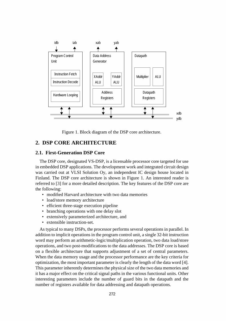
2. DSP CORE ARCHITECTURE
2.1. First-Generation DSP Core
The DSP core, designated VS-DSP, is a licensable processor core targeted for usein embedded DSP applications. The development work and integrated circuit designwas carried out at VLSI Solution Oy, an independent IC design house located inFinland. The DSP core architecture is shown in Figure 1. An interested reader isreferred to [3] for a more detailed description. The key features of the DSP core arethe following:
• modified Harvard architecture with two data memories• load/store memory architecture• efficient three-stage execution pipeline• branching operations with one delay slot• extensively parameterized architecture, and• extensible instruction-set.
As typical to many DSPs, the processor performs several operations in parallel. Inaddition to implicit operations in the program control unit, a single 32-bit instructionword may perform an arithmetic-logic/multiplication operation, two data load/storeoperations, and two post-modifications to the data addresses. The DSP core is basedon a flexible architecture that supports adjustment of a set of central parameters.When the data memory usage and the processor performance are the key criteria foroptimization, the most important parameter is clearly the length of the data word [4].This parameter inherently determines the physical size of the two data memories andit has a major effect on the critical signal paths in the various functional units. Otherinteresting parameters include the number of guard bits in the datapath and thenumber of registers available for data addressing and datapath operations.
yab
Figure 1. Block diagram of the DSP core architecture.
Hardware Looping
Program Control
Unit
Instruction Fetch
Instruction DecodeXAddr
ALU
Data Address
Generator
Address
Registers
YAddr
ALU
Multiplier
Datapath
Datapath
Registers
ALU
xabiabidb
xdbydb
272
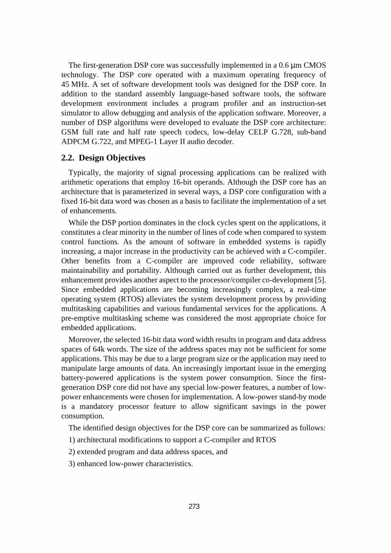
The first-generation DSP core was successfully implemented in a 0.6 µm CMOStechnology. The DSP core operated with a maximum operating frequency of45 MHz. A set of software development tools was designed for the DSP core. Inaddition to the standard assembly language-based software tools, the softwaredevelopment environment includes a program profiler and an instruction-setsimulator to allow debugging and analysis of the application software. Moreover, anumber of DSP algorithms were developed to evaluate the DSP core architecture:GSM full rate and half rate speech codecs, low-delay CELP G.728, sub-bandADPCM G.722, and MPEG-1 Layer II audio decoder.
2.2. Design Objectives
Typically, the majority of signal processing applications can be realized witharithmetic operations that employ 16-bit operands. Although the DSP core has anarchitecture that is parameterized in several ways, a DSP core configuration with afixed 16-bit data word was chosen as a basis to facilitate the implementation of a setof enhancements.
While the DSP portion dominates in the clock cycles spent on the applications, itconstitutes a clear minority in the number of lines of code when compared to systemcontrol functions. As the amount of software in embedded systems is rapidlyincreasing, a major increase in the productivity can be achieved with a C-compiler.Other benefits from a C-compiler are improved code reliability, softwaremaintainability and portability. Although carried out as further development, thisenhancement provides another aspect to the processor/compiler co-development [5].Since embedded applications are becoming increasingly complex, a real-timeoperating system (RTOS) alleviates the system development process by providingmultitasking capabilities and various fundamental services for the applications. Apre-emptive multitasking scheme was considered the most appropriate choice forembedded applications.
Moreover, the selected 16-bit data word width results in program and data addressspaces of 64k words. The size of the address spaces may not be sufficient for someapplications. This may be due to a large program size or the application may need tomanipulate large amounts of data. An increasingly important issue in the emergingbattery-powered applications is the system power consumption. Since the first-generation DSP core did not have any special low-power features, a number of low-power enhancements were chosen for implementation. A low-power stand-by modeis a mandatory processor feature to allow significant savings in the powerconsumption.
The identified design objectives for the DSP core can be summarized as follows:
1) architectural modifications to support a C-compiler and RTOS
2) extended program and data address spaces, and
3) enhanced low-power characteristics.
273
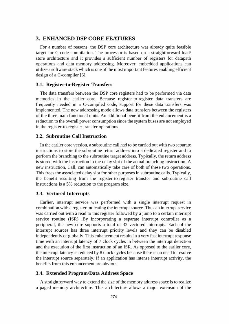
3. ENHANCED DSP CORE FEATURES
For a number of reasons, the DSP core architecture was already quite feasibletarget for C-code compilation. The processor is based on a straightforward load/store architecture and it provides a sufficient number of registers for datapathoperations and data memory addressing. Moreover, embedded applications canutilize a software stack which is one of the most important features enabling efficientdesign of a C-compiler [6].
3.1. Register-to-Register Transfers
The data transfers between the DSP core registers had to be performed via datamemories in the earlier core. Because register-to-register data transfers arefrequently needed in a C-compiled code, support for these data transfers wasimplemented. The new addressing mode allows data transfers between the registersof the three main functional units. An additional benefit from the enhancement is areduction to the overall power consumption since the system buses are not employedin the register-to-register transfer operations.
3.2. Subroutine Call Instruction
In the earlier core version, a subroutine call had to be carried out with two separateinstructions to store the subroutine return address into a dedicated register and toperform the branching to the subroutine target address. Typically, the return addressis stored with the instruction in the delay slot of the actual branching instruction. Anew instruction, Call, can automatically take care of both of these two operations.This frees the associated delay slot for other purposes in subroutine calls. Typically,the benefit resulting from the register-to-register transfer and subroutine callinstructions is a 5% reduction to the program size.
3.3. Vectored Interrupts
Earlier, interrupt service was performed with a single interrupt request incombination with a register indicating the interrupt source. Thus an interrupt servicewas carried out with a read to this register followed by a jump to a certain interruptservice routine (ISR). By incorporating a separate interrupt controller as aperipheral, the new core supports a total of 32 vectored interrupts. Each of theinterrupt sources has three interrupt priority levels and they can be disabledindependently or globally. This enhancement results in a very fast interrupt responsetime with an interrupt latency of 7 clock cycles in between the interrupt detectionand the execution of the first instruction of an ISR. As opposed to the earlier core,the interrupt latency is reduced by 8 clock cycles because there is no need to resolvethe interrupt source separately. If an application has intense interrupt activity, thebenefits from this enhancement are obvious.
3.4. Extended Program/Data Address Space
A straightforward way to extend the size of the memory address space is to realizea paged memory architecture. This architecture allows a major extension of the
274
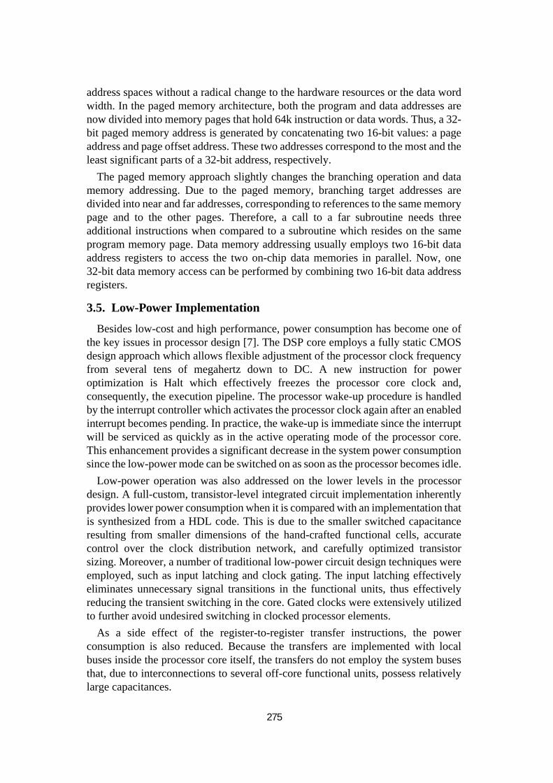
address spaces without a radical change to the hardware resources or the data wordwidth. In the paged memory architecture, both the program and data addresses arenow divided into memory pages that hold 64k instruction or data words. Thus, a 32-bit paged memory address is generated by concatenating two 16-bit values: a pageaddress and page offset address. These two addresses correspond to the most and theleast significant parts of a 32-bit address, respectively.
The paged memory approach slightly changes the branching operation and datamemory addressing. Due to the paged memory, branching target addresses aredivided into near and far addresses, corresponding to references to the same memorypage and to the other pages. Therefore, a call to a far subroutine needs threeadditional instructions when compared to a subroutine which resides on the sameprogram memory page. Data memory addressing usually employs two 16-bit dataaddress registers to access the two on-chip data memories in parallel. Now, one32-bit data memory access can be performed by combining two 16-bit data addressregisters.
3.5. Low-Power Implementation
Besides low-cost and high performance, power consumption has become one ofthe key issues in processor design [7]. The DSP core employs a fully static CMOSdesign approach which allows flexible adjustment of the processor clock frequencyfrom several tens of megahertz down to DC. A new instruction for poweroptimization is Halt which effectively freezes the processor core clock and,consequently, the execution pipeline. The processor wake-up procedure is handledby the interrupt controller which activates the processor clock again after an enabledinterrupt becomes pending. In practice, the wake-up is immediate since the interruptwill be serviced as quickly as in the active operating mode of the processor core.This enhancement provides a significant decrease in the system power consumptionsince the low-power mode can be switched on as soon as the processor becomes idle.
Low-power operation was also addressed on the lower levels in the processordesign. A full-custom, transistor-level integrated circuit implementation inherentlyprovides lower power consumption when it is compared with an implementation thatis synthesized from a HDL code. This is due to the smaller switched capacitanceresulting from smaller dimensions of the hand-crafted functional cells, accuratecontrol over the clock distribution network, and carefully optimized transistorsizing. Moreover, a number of traditional low-power circuit design techniques wereemployed, such as input latching and clock gating. The input latching effectivelyeliminates unnecessary signal transitions in the functional units, thus effectivelyreducing the transient switching in the core. Gated clocks were extensively utilizedto further avoid undesired switching in clocked processor elements.
As a side effect of the register-to-register transfer instructions, the powerconsumption is also reduced. Because the transfers are implemented with localbuses inside the processor core itself, the transfers do not employ the system busesthat, due to interconnections to several off-core functional units, possess relativelylarge capacitances.
275

Moreover, the semiconductor manufacturing process was updated to a 0.35 µmtriple-metal CMOS technology. In addition to higher circuit performance, theadvanced technology enables the use of lower supply voltages in the 1.1 - 3.3 Vrange. Clearly, the lower supply voltages have the most radical impact on the powerconsumption of the DSP core, program/data memories and other peripherals. A full-custom implementation of the DSP core, shown in Figure 2, contains 64000transistors and it occupies a die area of 2.2 mm2. With a 3.3 V supply voltage, theDSP core is expected to operate at a 100 MHz clock frequency.
The new features did not add any speed penalty to the processor. The newinstructions for register-to-register transfers and subroutine calls required amodification in the instruction decoding and the paged memory architecture addeda block of logic. Interestingly, the first-generation core layout had a relatively largeunused area in the instruction decoding section. For this reason, it was possible toplace most of the new features without increasing the core area. However, theinterrupt controller needs to be included as an off-core peripheral.
4. OPTIMIZING C-COMPILER
VS-DSP C-compiler (VCC) is an optimizing ANSI-C compiler targetedespecially for the VS-DSP architecture. The flow of operation in the DSP codegeneration is shown in Figure 3.
The C-compilation can be divided into three logical steps: general C-codeoptimization, assembly code generation, and assembly code optimization. Inaddition to syntax analysis, the general optimizer performs the common C-compileroperations, such as constant subexpression evaluation, logical expression
Figure 2. Chip layout of the enhanced DSP core.
DATAPATH
INSTRUCTIONDECODE
INSTRUCTIONFETCH
DATA ADDRESSGENERATOR
CLKPAGELOGIC
276
optimization, and jump condition reversal. The code generator allocates differentvariables to registers and data memories and it generates assembly code for all theintegral arithmetic and control structures. Depending on the structure of the programloops, the looping can be carried out as either hardware looping or in software. Thegenerated assembly code is then forwarded to the code optimizer. The codeoptimizer sequentially examines the assembly code, trying to make it more efficientby parallelizing various operations, filling delay slots in the branching instructionsand merging stack management instructions. From the raw instruction word count,the code optimizer can typically eliminate 20–30% of the instruction words.
In a C source code, various methods can be employed to guide the C-compiler toachieve more optimal results. For example, the execution speed of the criticalprogram sections can be increased considerably by forcing certain variables tospecific registers in the datapath and data address generator. However, at least theDSP algorithm kernels should be hand-coded in assembly language because thoseprogram sections contribute the most to the execution time of the applications.
5. REAL-TIME OPERATING SYSTEM
A real-time operating system (VS-RTOS) is a compact system kernel providingpre-emptive multitasking and a wide range of fundamental services for embeddedapplications. The key features of the RTOS are summarized in Table 1.
In pre-emptive multitasking, the RTOS determines when to change the runningtask and which one is the next task to be executed [8],[9]. However, the RTOS limits
Figure 3. Code generation with the C-Compiler.
Source C-Code
General Optimizer
Code Generator
Code Optimizer
Linking
Binary Executable
RTOS Kernel
C-Libraries
User Libraries
C-Compiler
Assembler
Linker
Code Assembly
277
the execution time of the tasks to a user-defined quantum of time when time-slicedscheduling is used. A system timer has to be included as an additional peripheral fortime-slicing. Typically, the system timer has a resolution of 1 ms and one time-slicecorresponds to 20 system timer intervals, i.e., 20 ms. For each of the tasks, anarbitrary number of time-slices can be allocated. Additionally, the RTOS supportssoftware timers. The correct operation of the RTOS has been demonstrated withseveral hardware prototypes. It is imperative to have a fully functional prototypesince the correct system behavior with multiple interrupts is practically impossibleto verify by means of simulations.
6. EMBEDDED SYSTEM DEVELOPMENT
Software development flow for the DSP core is quite straightforward. Theapplication code is programmed in C and assembly languages. The programs caneffectively be run in an instruction-set simulator (ISS). The ISS supports theparameterized architecture of the DSP and it also allows system simulation withbehavioral models of the off-core peripherals. After a cycle-accurate simulation withthe ISS, a profiler can be employed to analyze the dynamic run-time behavior of theapplication code. The information provided by the profiler enables identification ofthe program sections that would gain most from further optimization.
Although the ISS is capable of executing the program code at over 100000instructions per second, the highest execution speed can be achieved with ahardware emulator. An emulator program, which runs on a host PC, utilizes a DSPevaluation board to enable application prototyping with real-time input and output.The DSP evaluation board is equipped with a DSP prototype chip, externalmemories, miscellaneous digital/analog interfaces and an FPGA chip. A detailedsummary of the DSP evaluation board features is listed in Table 2.
In order to access off-chip memory devices, the DSP core includes an external bus
Table 1: RTOS Kernel Features.
Multitasking Pre-emptive
Time-sliced*
IntertaskCommunication
SignalsMessagesSemaphores
Memory Management DynamicAllocated in Fixed-sized Blocks
Full Context-Switch 87 clock cycles(0.87 µs @ 100 MHz)
ROM Memory Requirement 1355 words
RAM Memory Requirement 39 words
* optional, requires a system timer for scheduling
278

interface (EBI). The EBI has a 24-bit address space and it can insert processor wait-states to realize slow external memory accesses. The FPGA chip on the board has atypical capacity of 40k logic gates. A programmable logic device on the DSPevaluation board enables flexible system development and prototypingsimultaneously with some supplementary functions implemented in an application-specific hardware block. The DSP evaluation board has already proven itsapplicability in the development of several system prototypes. For example, theboard has recently been utilized to demonstrate the operation of an MPEG audiodecoder [10]. The audio decoder performs decoding of a 128kbit/s Layer III stream(44.1 kHz, stereo) at a 18 MHz clock frequency.
7. CONCLUSIONS
This paper presented a number of issues involved in the further development of acommercial DSP core. The selected enhancements addressed several aspects in theprocessor architecture. A number of new instructions were added to facilitate theexecution of those operations that are frequently required in C-compiler generatedprogram code. Improved support for fast interrupt services were realized with aninterrupt controller peripheral. This feature is mainly targeted to facilitate thedevelopment of the RTOS. Low-power characteristics of the processor core wereenhanced in several ways. One of the most important characteristics is a low-powerstand-by mode.
The implementation of the new features did not add any speed penalty to the DSPcore. The interrupt controller and the optional system timer were included as off-core peripherals. All the other enhancement were merged to the existing circuit
Table 2: Main features of the DSP evaluation board.
DSPPrototypeChip
ProcessorCore
16-bit VS-DSP CoreFour 40-bit AccumulatorsEight Data Address RegistersHardware Looping
Memories Data Memory: 2 x 16k RAMProgram Memory: 4k RAM, 4k ROM
Peripherals Synchronous Serial PortTwo RS232 Serial Ports8-bit Parallel PortSix 32-bit TimersKeyboard InterfaceInterrupt ControllerExternal Bus Interface
OtherBoardComponents
1M x 16-bit Flash Memory64k x 16-bit SRAMAltera Flex 10K40 FPGA2 x 16-bit DAC2 x 16-bit ADC25-button Keyboard
279
layout of the first-generation DSP core because unused circuit area was available forthese purposes.
References[1] Hitachi Micro Systems, Inc., SH-DSP Microprocessor Overview, Product
Databook, Revision 0.1, Nov. 1996.
[2] D. Walsh, "’Piccolo’ - The ARM Architecture for Signal Processing: anInnovative New Architecture for Unified DSP and MicrocontrollerProcessing," in Proc. Int. Conf. on Signal Processing Applications andTechnology, Boston, MA, U.S.A., Oct. 1996, pp. 658-663.
[3] J. Nurmi and J. Takala, "A New Generation of Parameterized and ExtensibleDSP Cores," in Proc. IEEE Workshop on Signal Processing Systems, Leicester,United Kingdom, Nov. 1997, pp. 320-329.
[4] M. Kuulusa, J. Nurmi, J. Takala, P. Ojala, and H. Herranen, "A Flexible DSPCore for Embedded Systems," IEEE Design & Test of Computers, vol. 14, no.4, pp. 60-68, Oct./Dec. 1997.
[5] H. Meyr, "On Core and More: A Design Perspective for System-on-Chip," inProc. IEEE Workshop on Signal Processing Systems, Leicester, UnitedKingdom, Nov. 1997, pp. 60-63.
[6] B.-S. Ovadia and Y. Be’ery, "Statistical Analysis as a Quantitative Basis forDSP Architecture Design," in VLSI Signal Processing, VII, J. Rabaey, P. M.Chau, J. Eldon, Eds., pp. 93-102. IEEE Press, New York, NY, U.S.A., 1994.
[7] J. M. Rabaey, Digital Integrated Circuits: A Design Perspective, Prentice-Hall,Upper Saddle River, NJ, U.S.A., 1996.
[8] J. A. Stankovic, "Misconceptions About Real-Time Computing,” Computer,vol. 21, no. 10, pp. 10-19, Oct. 1988.
[9] W. Zhao, K. Ramamritham, and J. Stankovic, "Scheduling Tasks WithResource Requirements in Hard Real-Time Systems,” IEEE Trans. onSoftware Engineering, vol. 13, no. 5, pp. 564-576, May 1987.
[10] ISO/IEC 11172-3, “Information technology - Coding of moving pictures andassociated audio for digital storage media at up to about 1.5 Mbit/s - Part 3:Audio,” Standard, International Organization for Standardization, Geneva,Switzerland, Mar. 1993.
280

PUBLICATION 6
M. Kuulusa, J. Takala, and J. Saarinen, “Run-time configurable hardware model in a dataflow
simulation,” in Proc. IEEE Asia-Pacific Conference on Circuits and Systems, Chiangmai,
Thailand, Nov. 24–27 1998, pp. 763–766.
Copyright c©1998 IEEE. Reprinted, with permission, from the proceedings of APCCAS’98.

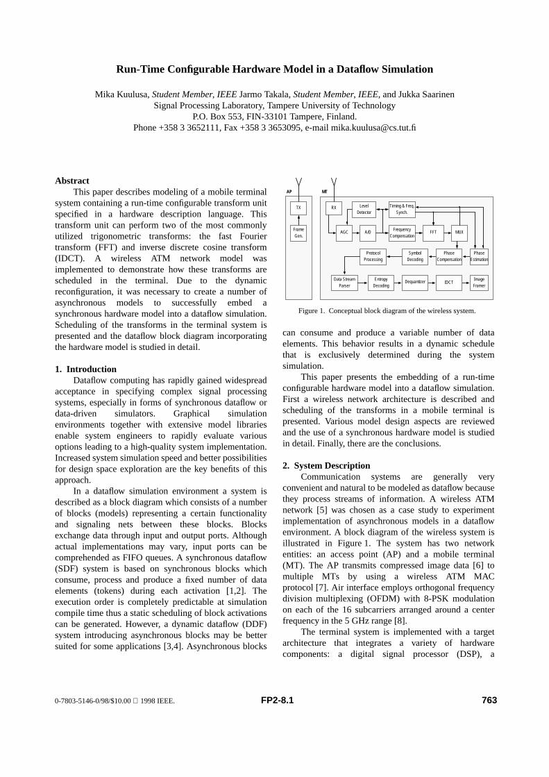
AbstractThis paper describes modeling of a mobile terminal
system containing a run-time configurable transform unitspecified in a hardware description language. Thistransform unit can perform two of the most commonlyutilized trigonometric transforms: the fast Fouriertransform (FFT) and inverse discrete cosine transform(IDCT). A wireless ATM network model wasimplemented to demonstrate how these transforms arescheduled in the terminal. Due to the dynamicreconfiguration, it was necessary to create a number ofasynchronous models to successfully embed asynchronous hardware model into a dataflow simulation.Scheduling of the transforms in the terminal system ispresented and the dataflow block diagram incorporatingthe hardware model is studied in detail.
1. IntroductionDataflow computing has rapidly gained widespread
acceptance in specifying complex signal processingsystems, especially in forms of synchronous dataflow ordata-driven simulators. Graphical simulationenvironments together with extensive model librariesenable system engineers to rapidly evaluate variousoptions leading to a high-quality system implementation.Increased system simulation speed and better possibilitiesfor design space exploration are the key benefits of thisapproach.
In a dataflow simulation environment a system isdescribed as a block diagram which consists of a numberof blocks (models) representing a certain functionalityand signaling nets between these blocks. Blocksexchange data through input and output ports. Althoughactual implementations may vary, input ports can becomprehended as FIFO queues. A synchronous dataflow(SDF) system is based on synchronous blocks whichconsume, process and produce a fixed number of dataelements (tokens) during each activation [1,2]. Theexecution order is completely predictable at simulationcompile time thus a static scheduling of block activationscan be generated. However, a dynamic dataflow (DDF)system introducing asynchronous blocks may be bettersuited for some applications [3,4]. Asynchronous blocks
can consume and produce a variable number of dataelements. This behavior results in a dynamic schedulethat is exclusively determined during the systemsimulation.
This paper presents the embedding of a run-timeconfigurable hardware model into a dataflow simulation.First a wireless network architecture is described andscheduling of the transforms in a mobile terminal ispresented. Various model design aspects are reviewedand the use of a synchronous hardware model is studiedin detail. Finally, there are the conclusions.
2. System DescriptionCommunication systems are generally very
convenient and natural to be modeled as dataflow becausethey process streams of information. A wireless ATMnetwork [5] was chosen as a case study to experimentimplementation of asynchronous models in a dataflowenvironment. A block diagram of the wireless system isillustrated in Figure 1. The system has two networkentities: an access point (AP) and a mobile terminal(MT). The AP transmits compressed image data [6] tomultiple MTs by using a wireless ATM MACprotocol [7]. Air interface employs orthogonal frequencydivision multiplexing (OFDM) with 8-PSK modulationon each of the 16 subcarriers arranged around a centerfrequency in the 5 GHz range [8].
The terminal system is implemented with a targetarchitecture that integrates a variety of hardwarecomponents: a digital signal processor (DSP), a
Figure 1. Conceptual block diagram of the wireless system.
AP MT
RX
FrequencyCompensation
FFTAGC MUXA/D
Timing & Freq.Synch.
LevelDetector
SymbolDecoding
PhaseCompensation
PhaseEstimation
ProtocolProcessing
Data StreamParser
EntropyDecoding
Dequantizer IDCT
TX
FrameGen.
ImageFramer
Run-Time Configurable Hardware Model in a Dataflow Simulation
Mika Kuulusa, Student Member, IEEE Jarmo Takala, Student Member, IEEE, and Jukka SaarinenSignal Processing Laboratory, Tampere University of Technology
P.O. Box 553, FIN-33101 Tampere, Finland.Phone +358 3 3652111, Fax +358 3 3653095, e-mail [email protected]
0-7803-5146-0/98/$10.00 1998 IEEE. FP2-8.1 763

microcontroller (MCU), a hardware accelerator, and aradio frequency front-end. Tasks with hard real-timerequirements, i.e., baseband signal processing anddecoding of the image data stream, are performed by theDSP. The MCU is used for system tasks with lessstringent real-time requirements, such as protocolprocessing and user interfaces. There are twofundamental transform operations required in an MT: fastFourier transform (FFT) for decoding OFDM symbols,and inverse discrete cosine transform (IDCT) needed inimage decompression. In our system, both of thesetransforms are effectively performed with an application-specific hardware accelerator. During the systemoperation this transform unit is configured in real-time toexecute transforms in a time-multiplexed fashion.
2.1. System SchedulingMedium access scheme in the modeled wireless
system utilizes time division multiple access [7]. Thecommunication is based on a variable length time framewhich contains a frame header and periods for downlinkand uplink transmission. The structure of the time frameand the transform scheduling is shown in Figure 2.
A time frame contains an integer number of timeslots. Each time slot contains 18 OFDM symbols that canbe special symbols used in a training sequence or 54octets of information. The frame header consumes asingle time slot and contains a special training sequence.During the downlink period the AP transmits informationin the form of user data bursts. A user data burst iscomposed of a header and data body. The header containsnecessary information about the burst and the structure ofthe current time frame. The data body is used to transportcompressed image data. In our simulation model, weassume that no transmission activity exists in the uplinkperiod.
A protocol processor controls scheduling of thetransform unit in the system. After the received signal ismixed, filtered, and down converted it is possible to
recover the differentially encoded OFDM symbols byusing a complex valued 16-point FFT. Therefore, thesignal reception is enabled only by executing an FFToperation to decode OFDM symbols. The principlebehind the transform scheduling is to execute an FFToperation always when it is needed and perform an IDCToperation when the transform unit is idle.
The protocol processing operates in the followingmanner. First, the receiver detects the beginning of a newtime frame by identifying the training sequence. Then itstarts scanning the user data headers. If the destinationaddress in a header does not match, the next time slotscontaining the data body are skipped. When a burst witha correct destination address is found, the data burst isdecoded and the remaining time slots can be scheduled toperform IDCT operations. Additionally, IDCT operationsare permitted in the time slots that are skipped during theheader scanning. Because IDCT operations areperformed only in the vacant time slots, the system mustbe capable of buffering frequency coefficients extractedfrom the image data stream. In the case no coefficientsare available, the transform unit stays idle until it is againrequired for symbol decoding.
2.2. Regular Trigonometric Transform UnitRegular trigonometric transform (RTT) unit is a
configurable hardware accelerator which can be utilizedto perform either a complex valued 16-point FFT or a8x8-point IDCT. The structure of the RTT unit is basedon a constant geometry architecture that consists ofconfigurable processor elements and a dynamicpermutation network [9,10].
Before a certain transform can be executed, it maybe necessary to switch the hardware configuration fromone transform to another. This change of hardwareoperation takes one clock cycle. The RTT unit operates inpipelined fashion: the operations are executed by firstforwarding the input data, eight values in parallel, to thehardware, and then clocking the unit a certain number ofclock cycles to iteratively perform the required transformoperation. However, it should be noted that the input datavalues must be arranged into a transform-specific orderbefore they can be passed to the hardware. In addition,output values resulting from an operation also need somerearranging.
The RTT unit executes a complex valued 16-pointFFT in 18 clock cycles. The first four cycles arenecessary to pass 32 input data values, split into 16 realand imaginary components. In the remaining 14 cyclesthe hardware performs the FFT operation. The imagedecompression is realized by executing a two-dimensional (2-D) IDCT to a block of 8x8 frequencycoefficients which are provided by an image data streamparser. It is of common practice to perform this 2-D
Figure 2. Scheduling of the transform operations in a mobile terminal.
Downlink Period
ReceivedSignal
FFT
IDCT
Uplink Period
Variable Length Time Frame
Scheduled Transform
IDCTPermitted
ExecuteFFT
764 FP2-8.2
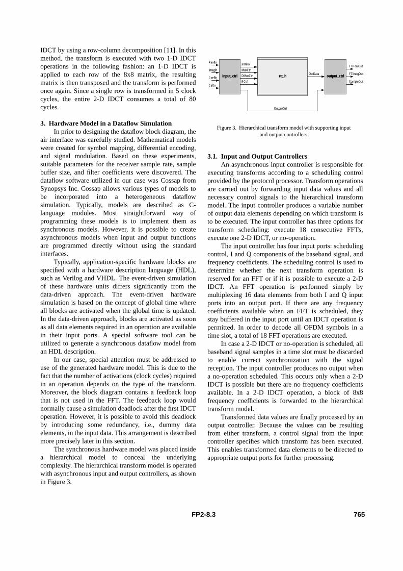
IDCT by using a row-column decomposition [11]. In thismethod, the transform is executed with two 1-D IDCToperations in the following fashion: an 1-D IDCT isapplied to each row of the 8x8 matrix, the resultingmatrix is then transposed and the transform is performedonce again. Since a single row is transformed in 5 clockcycles, the entire 2-D IDCT consumes a total of 80cycles.
3. Hardware Model in a Dataflow SimulationIn prior to designing the dataflow block diagram, the
air interface was carefully studied. Mathematical modelswere created for symbol mapping, differential encoding,and signal modulation. Based on these experiments,suitable parameters for the receiver sample rate, samplebuffer size, and filter coefficients were discovered. Thedataflow software utilized in our case was Cossap fromSynopsys Inc. Cossap allows various types of models tobe incorporated into a heterogeneous dataflowsimulation. Typically, models are described as C-language modules. Most straightforward way ofprogramming these models is to implement them assynchronous models. However, it is possible to createasynchronous models when input and output functionsare programmed directly without using the standardinterfaces.
Typically, application-specific hardware blocks arespecified with a hardware description language (HDL),such as Verilog and VHDL. The event-driven simulationof these hardware units differs significantly from thedata-driven approach. The event-driven hardwaresimulation is based on the concept of global time whereall blocks are activated when the global time is updated.In the data-driven approach, blocks are activated as soonas all data elements required in an operation are availablein their input ports. A special software tool can beutilized to generate a synchronous dataflow model froman HDL description.
In our case, special attention must be addressed touse of the generated hardware model. This is due to thefact that the number of activations (clock cycles) requiredin an operation depends on the type of the transform.Moreover, the block diagram contains a feedback loopthat is not used in the FFT. The feedback loop wouldnormally cause a simulation deadlock after the first IDCToperation. However, it is possible to avoid this deadlockby introducing some redundancy, i.e., dummy dataelements, in the input data. This arrangement is describedmore precisely later in this section.
The synchronous hardware model was placed insidea hierarchical model to conceal the underlyingcomplexity. The hierarchical transform model is operatedwith asynchronous input and output controllers, as shownin Figure 3.
3.1. Input and Output ControllersAn asynchronous input controller is responsible for
executing transforms according to a scheduling controlprovided by the protocol processor. Transform operationsare carried out by forwarding input data values and allnecessary control signals to the hierarchical transformmodel. The input controller produces a variable numberof output data elements depending on which transform isto be executed. The input controller has three options fortransform scheduling: execute 18 consecutive FFTs,execute one 2-D IDCT, or no-operation.
The input controller has four input ports: schedulingcontrol, I and Q components of the baseband signal, andfrequency coefficients. The scheduling control is used todetermine whether the next transform operation isreserved for an FFT or if it is possible to execute a 2-DIDCT. An FFT operation is performed simply bymultiplexing 16 data elements from both I and Q inputports into an output port. If there are any frequencycoefficients available when an FFT is scheduled, theystay buffered in the input port until an IDCT operation ispermitted. In order to decode all OFDM symbols in atime slot, a total of 18 FFT operations are executed.
In case a 2-D IDCT or no-operation is scheduled, allbaseband signal samples in a time slot must be discardedto enable correct synchronization with the signalreception. The input controller produces no output whena no-operation scheduled. This occurs only when a 2-DIDCT is possible but there are no frequency coefficientsavailable. In a 2-D IDCT operation, a block of 8x8frequency coefficients is forwarded to the hierarchicaltransform model.
Transformed data values are finally processed by anoutput controller. Because the values can be resultingfrom either transform, a control signal from the inputcontroller specifies which transform has been executed.This enables transformed data elements to be directed toappropriate output ports for further processing.
Figure 3. Hierarchical transform model with supporting inputand output controllers.
InData
MuxCtrl
DMuxCtrl
RCtrl
input_ctrl rtt_h output_ctrl
RealIn
ImagIn
CoefIn
CtrlIn
FTRealOut
FTImagOut
SampleOut
OutData
OutputCtrl
FP2-8.3 765
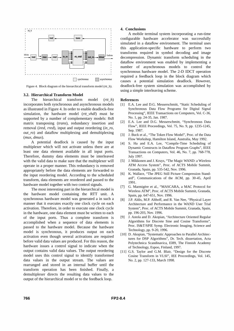
3.2. Hierarchical Transform ModelThe hierarchical transform model (rtt_h)
incorporates both synchronous and asynchronous modelsas illustrated in Figure 4. In order to enable deadlock-freesimulation, the hardware model (rtt_vhdl) must besupported by a number of complementary models: 8x8matrix transposing (trans), redundancy insertion andremoval (ired, rred), input and output reordering (in_ro,out_ro) and dataflow multiplexing and demultiplexing(mux, dmux).
A potential deadlock is caused by the inputmultiplexer which will not activate unless there are atleast one data element available in all input ports.Therefore, dummy data elements must be interleavedwith the valid data to make sure that the multiplexer willoperate in a proper manner. This redundancy is removedappropriately before the data elements are forwarded tothe input reordering model. According to the scheduledtransform, data elements are reordered and passed to thehardware model together with two control signals.
The most interesting part in the hierarchical model isthe hardware model containing the RTT unit. Asynchronous hardware model was generated a in such amanner that it executes exactly one clock cycle on eachactivation. Therefore, in order to execute one clock cyclein the hardware, one data element must be written to eachof the input ports. Thus a complete transform isaccomplished when a sequence of data elements ispassed to the hardware model. Because the hardwaremodel is synchronous, it produces output on eachactivation even though several activations are requiredbefore valid data values are produced. For this reason, thehardware issues a control signal to indicate when theoutput contains valid data values. The output reorderingmodel uses this control signal to identify transformeddata values in the output stream. The values arerearranged and stored in an internal buffer until thetransform operation has been finished. Finally, ademultiplexer directs the resulting data values to theoutput of the hierarchical model or to the feedback loop.
4. ConclusionsA mobile terminal system incorporating a run-time
configurable hardware accelerator was successfullysimulated in a dataflow environment. The terminal usesthis application-specific hardware to perform twotransforms required in symbol decoding and imagedecompression. Dynamic transform scheduling in thedataflow environment was enabled by implementing anumber of asynchronous models to control thesynchronous hardware model. The 2-D IDCT operationrequired a feedback loop in the block diagram whichcauses a potential simulation deadlock. However,deadlock-free system simulation was accomplished byusing a simple interleaving scheme.
References[1] E.A. Lee and D.G. Messerschmitt, “Static Scheduling of
Synchronous Data Flow Programs for Digital SignalProcessing”, IEEE Transactions on Computers, Vol. C-36,No. 1, pp. 24-35, Jan. 1987.
[2] E.A. Lee and D.G. Messerschmitt, “Synchronous DataFlow”, IEEE Proceedings, Vol. 75, No. 9, pp. 1235-1245,Sep. 1987.
[3] J. Buck et al., “The Token Flow Model”, Proc. of the DataFlow Workshop, Hamilton Island, Australia, May 1992.
[4] S. Ha and E.A. Lee, “Compile-Time Scheduling ofDynamic Constructs in Dataflow Program Graphs”, IEEETransactions on Computers, Vol. 46, No. 7, pp. 768-778,July 1997.
[5] J. Mikkonen and J. Kruys, “The Magic WAND: a WirelessATM Access System”, Proc. of ACTS Mobile Summit,Granada, Spain, pp. 535-542, Nov. 1996.
[6] K. Wallace, “The JPEG Still Picture Compression Stand-ard”, Communications of the ACM, pp. 30-45, April1991.
[7] G. Marmigère et al., “MASCARA, a MAC Protocol forWireless ATM”, Proc. of ACTS Mobile Summit, Granada,Spain, pp. 647-651, Nov. 1996.
[8] J.P. Aldis, M.P. Althoff, and R. Van Nee, “Physical LayerArchitecture and Performance in the WAND User TrialSystem”, Proc. of ACTS Mobile Summit, Granada, Spain,pp. 196-203, Nov. 1996.
[9] J. Astola and D. Akopian, “Architecture Oriented RegularAlgorithms for Discrete Sine and Cosine Transforms”,Proc. IS&T/SPIE Symp. Electronic Imaging, Science andTechnology, pp. 9-20, 1996.
[10] D. Akopian, “Systematic Approaches to Parallel Architec-tures for DSP Algorithms”, Dr. Tech. dissertation, ActaPolytechnica Scandinavica, El89, The Finnish Academyof Technology, Espoo, Finland, 1997.
[11] G.S. Taylor and G.M. Blair, “Design for the DiscreteCosine Transform in VLSI”, IEE Proceedings, Vol. 145,No. 2, pp. 127-133, March 1998.
Figure 4. Block diagram of the hierarchical transform model (rtt_h).
rtt_vhdlin_ro out_ro
trans
ired mux rred dmux
ired
synchronous asynchronous
InData OutData
rtt_h
766 FP2-8.4

PUBLICATION 7
M. Kuulusa and J. Nurmi, “Baseband implementation aspects for W-CDMA mobile
terminals,” in Proc. Baiona Workshop on Emerging Technologies in Telecommunications,
Baiona, Spain, Sep. 6–8 1999, pp. 292–296.
Copyright c©1999 Servicio de Publicacions da Universidade de Vigo, Spain. Reprinted, with
permission, from the proceedings of BWETT’99.

ABSTRACT
This paper addresses several implementationaspects in the baseband section of a W-CDMA mobileterminal that is based on the UMTS terrestrial radioaccess (UTRA) radio transmission technology proposal.The objective was to construct suitable transceiverarchitectures for the next generation multi-modeterminals which support both TDD and FDD modes ofoperation.
1. INTRODUCTION
The third generation mobile communicationswill be based on code-division multiple access (CDMA).The future CDMA systems will employ 2 GHz carrierfrequencies in combination with a wide transmissionbandwidth to provide variable data rates of up to 2Mbit/s. Both packet and circuit-switched connectionswill be supported. In addition to conventional speechservice, high-speed data rates allow realization of adiverse set of multimedia and data services for thenext generation mobile terminals.
UTRA specification, also often more simplyreferred to as W-CDMA, is the European candidateproposal for the global standard of the W-CDMA airinterface [1]. UTRA employs direct-sequence spread-spectrum technology with a chip rate of 4.096 Mchip/sto spread quadrature phase-shift keyed (QPSK) datasymbols to a 5 MHz transmission bandwidth.Spectrum-spreading is performed with a combinationof complex and dual-channel spreading operations.Downlink (base station to mobile) and uplink (mobileto base station) transmissions are based on a 10 msframe that contains a total of 16 time slots. Thus atime slot corresponds to 0.625 ms or 2560 chips.Variable data rates can be realized either by allocatingseveral physical code channels for one user or byadjusting data rate of the physical code channel, i.e.,the spreading factor. These are called multi-code andvariable spreading factor methods, respectively.
First W-CDMA receiver implementations aremost likely to be based on conventional Rake receivers.In the past, Rake receivers have been utilized insystems for, e.g., wireless LANs [2,3,4,5], cellular [6],and space communications [7]. CDMA systems areinterference-limited because several users use thesame frequency band for transmissions. Therefore,conventional Rake receivers will be followed byadvanced receivers that implement sophisticatedinterference cancellation techniques, such assuccessive interference cancellation (SIC) or linearminimum mean-squared error (LMMSE) methods, toremove at least the dominant interferes causing themost of the multiple-access interference on the radiochannel.
In this paper, downlink receiver and uplinktransmitter architectures realizing the basebandsignal processing functions for W-CDMA mobileterminals are described. Although the implementationaspects presented in this paper are focused on theUTRA proposal, the architectures for the otherproposals will very similar those described in thefollowing sections.
2. TRANSCEIVER ARCHITECTURE FOR W-CDMA
According to downlink (DL) and uplink (UL)frequency usage, UTRA specifies two modes ofoperation: time-division duplex (TDD) and frequency-division duplex (FDD). The main differences betweenthese two modes are the following:
• DL/UL frequency allocation: TDD single band, FDD paired band
• DL/UL transmissions: TDD time-multiplexed, FDD continuous
• Placement of the DL pilot symbols: TDD midambles, FDD preambles
• Symbol spreading factors: TDD 1-16, FDD 4-256• Spreading code generators: TDD OVSF, FDD
OVSF/Gold/VL-Kasami• Symbol rates: TDD 256k - 4M symbol/s, FDD 16k-
1M symbol/s
BASEBAND IMPLEMENTATION ASPECTS FOR W-CDMA MOBILE TERMINALS
Mika Kuulusa and Jari Nurmi
Signal Processing LaboratoryTampere University of Technology,
P.O. Box 553 (Hermiankatu 12), FIN-33101 Tampere, FinlandFax +358 3 3653095, Tel. +358 3 3652111, E-mail: [email protected]
292
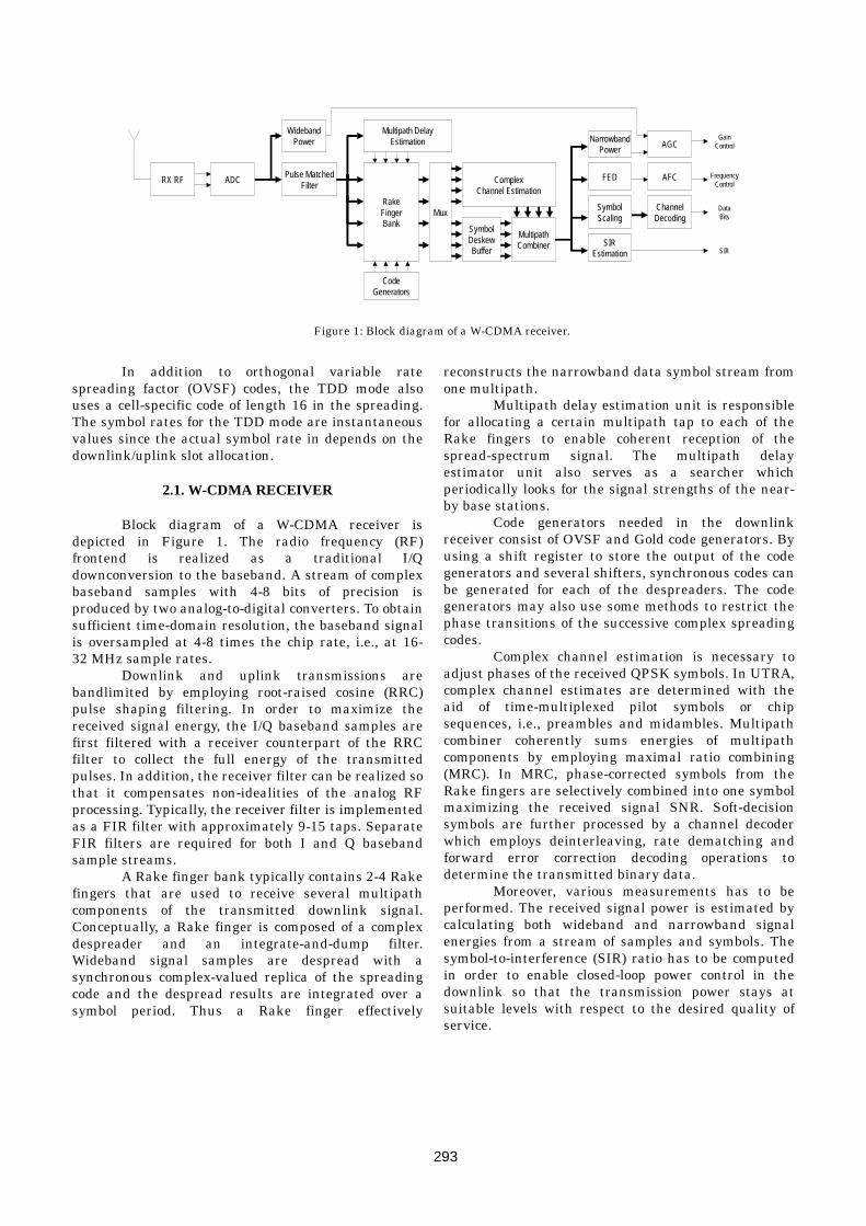
In addition to orthogonal variable ratespreading factor (OVSF) codes, the TDD mode alsouses a cell-specific code of length 16 in the spreading.The symbol rates for the TDD mode are instantaneousvalues since the actual symbol rate in depends on thedownlink/uplink slot allocation.
2.1. W-CDMA RECEIVER
Block diagram of a W-CDMA receiver isdepicted in Figure 1. The radio frequency (RF)frontend is realized as a traditional I/Qdownconversion to the baseband. A stream of complexbaseband samples with 4-8 bits of precision isproduced by two analog-to-digital converters. To obtainsufficient time-domain resolution, the baseband signalis oversampled at 4-8 times the chip rate, i.e., at 16-32 MHz sample rates.
Downlink and uplink transmissions arebandlimited by employing root-raised cosine (RRC)pulse shaping filtering. In order to maximize thereceived signal energy, the I/Q baseband samples arefirst filtered with a receiver counterpart of the RRCfilter to collect the full energy of the transmittedpulses. In addition, the receiver filter can be realized sothat it compensates non-idealities of the analog RFprocessing. Typically, the receiver filter is implementedas a FIR filter with approximately 9-15 taps. SeparateFIR filters are required for both I and Q basebandsample streams.
A Rake finger bank typically contains 2-4 Rakefingers that are used to receive several multipathcomponents of the transmitted downlink signal.Conceptually, a Rake finger is composed of a complexdespreader and an integrate-and-dump filter.Wideband signal samples are despread with asynchronous complex-valued replica of the spreadingcode and the despread results are integrated over asymbol period. Thus a Rake finger effectively
reconstructs the narrowband data symbol stream fromone multipath.
Multipath delay estimation unit is responsiblefor allocating a certain multipath tap to each of theRake fingers to enable coherent reception of thespread-spectrum signal. The multipath delayestimator unit also serves as a searcher whichperiodically looks for the signal strengths of the near-by base stations.
Code generators needed in the downlinkreceiver consist of OVSF and Gold code generators. Byusing a shift register to store the output of the codegenerators and several shifters, synchronous codes canbe generated for each of the despreaders. The codegenerators may also use some methods to restrict thephase transitions of the successive complex spreadingcodes.
Complex channel estimation is necessary toadjust phases of the received QPSK symbols. In UTRA,complex channel estimates are determined with theaid of time-multiplexed pilot symbols or chipsequences, i.e., preambles and midambles. Multipathcombiner coherently sums energies of multipathcomponents by employing maximal ratio combining(MRC). In MRC, phase-corrected symbols from theRake fingers are selectively combined into one symbolmaximizing the received signal SNR. Soft-decisionsymbols are further processed by a channel decoderwhich employs deinterleaving, rate dematching andforward error correction decoding operations todetermine the transmitted binary data.
Moreover, various measurements has to beperformed. The received signal power is estimated bycalculating both wideband and narrowband signalenergies from a stream of samples and symbols. Thesymbol-to-interference (SIR) ratio has to be computedin order to enable closed-loop power control in thedownlink so that the transmission power stays atsuitable levels with respect to the desired quality ofservice.
Figure 1: Block diagram of a W-CDMA receiver.
RX RF
GainControl
ADC
SymbolDeskewBuffer
RakeFingerBank
WidebandPower
MultipathCombiner
SymbolScaling
SIREstimation
FED
CodeGenerators
AFC
ChannelDecoding
AGC
ComplexChannel Estimation
NarrowbandPower
Mux
Multipath DelayEstimation
Pulse MatchedFilter
FrequencyControl
DataBits
SIR
293
By using successive data symbols, a frequencyerror detector (FED) produces an estimate of thefrequency error [8,9]. The output of the FED is passedto an automatic frequency control (AFC) algorithmwhich adjusts the frequency of local oscillator to that ofthe base station transmitter. Automatic gain control(AGC) is employed to rapidly adjust the input voltageto the ADCs so that the signal levels stay inappropriate range for proper reception. It should alsobe noted that the transmitter uses an estimate ofreceived signal strength to adjust the transmitterpower in the TDD mode.
2.2. W-CDMA TRANSMITTER
A W-CDMA transmitter for UTRA isconsiderably more straightforward when compared tothe receiver side. Basically, the transmitter can beconstructed with a simple dataflow structure thatcomprises of QPSK symbol mapping, complex/dual-channel spreading, transmitter pulse shaping andquadrature modulation operations, as shown inFigure 2. Due to paper length limitations, thetransmitter will not be studied in detail. However, aninteresting treatment on the pulse shaping filteringcan be found in [10].
3. HARDWARE IMPLEMENTATION ASPECTS
From the hardware implementation point ofview, the number representation of the I/Q samplesthroughout the receiver requires special attention.Traditionally, two’s complement representation hasbeen employed for its simplicity in arithmeticoperations. However, in a Rake receiver most of themultiplications are with performed with values of ±1. Ifthe samples are in two’s complement representation,the multiplication by -1 requires inversion of all bits ofthe sample and an addition by one. When a largenumber of these multiplications has to be performed ina Rake receiver, an alternative number representationmay be more appropriate when the power consumptionis considered. By employing sign-and-magnitude
number representation, the sign is effectively stored ina single bit. Thus a multiplication by ±1 can be realizedwith a single exclusive-or (XOR) logic operationresulting in a minimal hardware overhead.
True complex multiplications are employedonly in the multipath combiner which rotates andweights each of the multipath symbol with thecorresponding channel estimate.
3.1. FULL CODE-MATCHED FILTER
Due to rapidly changing mobile radio channels,fast code acquisition is crucial for the Rake receiverperformance. The most suitable acquisition device formultipath estimation is a full code-matched filter [11].The structure of the filter is depicted in Figure 3.Conceptually, the full code-matched filter is acorrelation device which effectively performs one largeparallel correlation of a given length with the I/Qsamples stored in two delay lines. A number ofcomplex-valued matching sequences are stored in aregister bank so that different matching sequences canbe rapidly selected.
Although the fundamental structure is quitesimple, the code-matched filter has to execute amassive amount of operations. For example, a filterrealizing matching to a complex code sequence of 256chips requires a total of 1024 multiply-accumulateoperations. At the chip rate, this corresponds to 4Gmultiply-accumulate operations per second. However,since the multiplications are performed with parallelXOR operations, the correlation reduces into a sum of1024 products. Moreover, further optimizations can be
Figure 3: Structure of the full code-matched filter
IsQs
Complex Matching Sequences
∑
| . |2
| . |2
Icorr
Qcorr
MultipathPower
Averaging
MultipathDelay Profile
. . .
. . .
D D D D D D
Figure 2: Block diagram of a W-CDMA transmitter.
TX RFDACChannelBits
PulseShaping
CodeGenerators
SpecialChip Sequences
QuadratureModulation
Spreading Scrambling
MuxSymbolMapping
294
made if the code sequence does not contain purecomplex values. For example, midamble chips arealternating real and imaginary in the TDD mode, thusreducing multiply-accumulate operations by half.
The output of the code-matched filter is furtherprocessed by a power estimator that employs anobservation window of finite length to create a powerestimates for each window position. In order to obtainreliable power estimates, the results are averaged. Themultipath estimation and averaging could cover thepilot sequences of 32 time slots. This would allow anupdate to the Rake finger allocation in 20 ms intervals.
3.2. RAKE FINGER
A complex despreader together with anintegrate-and-dump filter is depicted in Figure 4. Acomplex correlation is performed with a total fourmultiplications and two additions. The despreadsamples from one symbol period are summed in theaccumulator at the chip rate and the results aredumped out at the symbol rate.
A Rake finger employing sign-and-magnitudenumber representation of the samples is shown inFigure 5 [12]. The Rake finger can be convenientlydivided into despreader, integration and dumpsections. By using XOR sign-flips, the despreadermultiplies the I/Q samples with the spreading codesand employs two separate branches to accumulate thepositive and negative sums. The accumulation isperformed in carry-save arithmetic at the chip rate.
The final carry-propagate additions of the positive andnegative branches are carried out in the dump sectionwhich operates at a symbol rate.
3.3. SYMBOL DESKEW BUFFER
Because symbol dumps from the Rake fingersare asynchronous with respect to each other, a symbolbuffer is necessary to store time-skewed symbols fromdifferent multipaths [6]. In practice, the size of thebuffers is determined by the maximum allowable delayspread and the supported spreading factors. Assuminga minimum spreading factor of four and a delay spreadof 16 µs, the deskew buffer must have capacity for atleast 16 symbols. Moreover, a larger deskew buffer canbe used to store the first data part of the TDDdownlink burst because of the pilot sequence is locatedin the middle of the burst. After the first data part hasbeen received, the multiplexer routes the pilot to thechannel estimator. After the channel estimates havebeen calculated, the multipath combiner can proceed.
3.4. CHANNEL ESTIMATION
In UTRA, complex channel estimates is aredetermined with the known pilot symbols or certainchip sequences. The channel estimates are theninterpolated to provide valid estimates for the durationof a time slot. It may also be a feasible solution that thechannel estimator switches to a decision-directed modeafter initial estimation from the known pilot symbols.Moreover, the movement of the mobile receiver causesDoppler shifts to the multipath components.Interestingly, channel estimates can used tocompensate also for these frequency shifts that areapproximately 220 Hz at maximum for a mobile speedof 120 km/h.
Optimal channel estimator is a FIR filteressentially performing a moving average on a numberof received symbols [13]. However, also exponential tailtype IIR filters have been employed in some receivers.The channel estimator itself should be adaptive to thechanging conditions in the radio channel. Thus, thenumber of symbols in the averaging FIR filter and theloop gains in the IIR filters should be made adjustable.
3.5. MULTIPATH COMBINER
Multipath combiner uses the complexestimates from the channel estimation unit to producephase-corrected symbols. In addition to the phase-correction, the symbols are also multiplied with theestimates of the corresponding symbol magnitudes.Thus, the combiner effectively employs maximal-ratiocombining by simply summing the phase-corrected and
+
-I&D
Icode Qcode
+ I&D
IsIsym
Qsym
Figure 4: Rake finger with a complex despreader and integrate-and-dump filter
Qs
I code
Positive Sum
Is D CSAdd DD
DD
CSAdd
Qcode
Qs
D
D CSAdd DD
DDCSAdd
Negative Sum
+
+D
+ Isym
Figure 5: Partial implementation of a Rake finger (boxed section in Figure 4).
295

weighted data symbols from the Rake fingers. Themultipath combiner may also contain some decisionlogic to discard weak multipath components with lowSNR.
4. BASEBAND PARTITIONING FOR DSP/ASIC
The core of a W-CDMA mobile terminal will beimplemented as a system-on-a-chip (SOC) thatcontains programmable processors, dedicatedhardware accelerators, memories, peripherals, andmixed-signal devices to realize all the requiredfunctions. Depending on the terminal capabilities,such as transceiver performance, supported data ratesand multimedia capabilities, different trade-offs can bejustified. For example, an advanced multimediaterminal supporting 2 Mbit/s data rates has quitedifferent system requirements as opposed to a low-end144 kbit/s terminal.
The W-CDMA receiver and transmitterarchitectures can be divided into domains that operateat sample, chip, and symbol rates. Because the sample/chip rates are quite high and a high level of parallelismis needed, the receiver blocks that are most likely to beimplemented as dedicated application-specificintegrated circuits (ASICs) are the RRC filter, fullcode-matched filter, code generators, and the Rakefingers. Symbol dumps from the Rake fingers and theaveraged multipath tap profiles can be processed atrates that can be handled with a high-performancedigital signal processor (DSP). In addition to fast FIRfiltering operations, the latest DSPs calculate truecomplex multiplications effectively with their powerfuldatapaths comprising of two or even four multiply-accumulate units. Moreover, another benefit ofemploying a programmable DSP is the flexibility of theimplementation. When a DSP controls the generaloperation of the transceiver, the system can easily bemade adaptive to variable symbol rates and thechanging conditions on the radio channel. Thetransmitter implementation, however, will be heavilyhardware-oriented since the baseband operations arerelatively simple and short data word lengths can beemployed.
5. CONCLUSIONS
The presented W-CDMA transceiverarchitectures comprise of a number of blocks whichperform signal processing at the sample, chip andsymbol rates. Due to relatively high sample rates andthe level of parallelism, especially in the receiver, thefirst mobile terminals will be based on dedicatedhardware. The baseband blocks gaining most of ahardware implementation are those which can be
realized with simple parallel operations. From thereceiver architecture, the full code-matched filter andthe RRC filter are clearly the toughest parts to berealized. A programmable DSP provides flexible meansfor transceiver control and other system tasks.Moreover, a DSP can also take care of the symbol rateprocessing at relatively low data rates.
REFERENCES
[1] Tdoc SMG2 260/98, “The ETSI UMTS Terrestrial RadioAccess (UTRA) ITU-R RTT Candidate Submission,”European Telecommunications Standards Institute (ETSI),Sophia Antipolis, France, 1998.
[2] S.D. Lingwood, H. Kaufmann, and B. Haller, “ASICImplementation of a Direct-Sequence Spread-SpectrumRAKE-Receiver,” Proc. IEEE Vehicular TechnologyConference (VTC), 1994, pp. 1326-1330.
[3] D.T. Magill, “A Fully-Integrated, Digital, Direct Sequence,Spread Spectrum Modem ASIC,” Proc. IEEE InternationalSymposium on Personal, Indoor and Mobile RadioCommunications (PIMRC), 1992, pp. 42-46.
[4] J.S. Wu, M.L. Liou, H.P. Ma, and T.D. Chiueh, “A 2.6-V, 33-MHz All-Digital QPSK Direct Sequence Spread-SpectrumTransceiver IC,” IEEE Journal of Solid-State Circuits, Vol.32., No. 10., October 1997, pp. 1499-1510.
[5] H.M. Chang and M.H. Sunwoo, “Implementation of a DSSSModem ASIC Chip for Wireless LAN,” Proc. IEEE Workshopon Signal Processing Systems (SIPS) 1998, pp. 243-252.
[6] J.K. Hinderling et al., “CDMA Mobile Station Modem ASIC,”IEEE Journal of Solid-State Circuits, Vol. 28, No. 3, March1993, pp. 253-260.
[7] C. Uhl, J.J. Monot, and M. Margery, “Single ASIC Receiverfor Space Applications,” Proc. IEEE Vehicular TechnologyConference (VTC), 1994, pp. 1331-1335.
[8] H. Meyr, M. Moeneclaey, and S.A. Fechtel, DigitalCommunication Receivers: Synchronization, ChannelEstimation, and Signal Processing. New York: John Wiley &Sons Inc., 1998.
[9] U. Fawer, “A Coherent Spread-Spectrum RAKE-Receiverwith Maximum-Likelihood Frequency Estimation,” IEEEInternational Conference on Communications (ICC), 1992,pp. 471-475.
[10] G.L. Do and K. Feher, “Efficient Filter Design for IS-95CDMA Systems,” IEEE Transactions on ConsumerElectronics, Vol. 42, Issue 4, Nov. 1996, pp. 1011-1020.
[11] D.T. Magill and G. Edwards, “Digital Matched Filter ASIC,”Proc. Military Communications Conference (MILCOM),1990, pp. 235-238.
[12] S. Sheng and R. Brodersen, Low-Power CMOS WirelessCommunications: A Wideband CDMA System Design.Kluwer Academic Publishers, 1998.
[13] S.D. Lingwood, “A 65 MHz Digital Chip Matched Filter forDS-Spread Spectrum Applications,”, Proc. InternationalZurich Seminar (IZS), Zurich, Switzerland, March 1994, pp.1326-1330.
296