dual output digital multi-phase controller ir35211 output digital multi-phase controller ir35211 5 |...
TRANSCRIPT

Dual Output Digital Multi-Phase Controller IR35211
www.irf.com | © 2014 International Rectifier July 24, 2014 | V1.001
FEATURES
Dual output 3+1 phase PWM Controller
Easiest layout and fewest pins in the industry
Fully supports AMD® SVI1 & SVI2 with dual OCP and Intel® VR12 & VR12.5
Overclocking & Gaming Mode
Switching frequency from 200kHz to 2MHz per phase
IR Efficiency Shaping Features including Dynamic Phase Control and Automatic Power State Switching
Programmable 1-phase operation for Light Loads and Active Diode Emulation for Very Light Loads
IR Adaptive Transient Algorithm (ATA) on both loops minimizes output bulk capacitors and system cost
Auto-Phase Detection with auto-compensation
Per-Loop Fault Protection: OVP, UVP, OCP, OTP
I2C/SMBus/PMBus system interface for telemetry of Temperature, Voltage, Current & Power for both loops
Multiple Time Programming (MTP) with integrated charge pump for easy custom configuration
Compatible with IR ATL and 3.3V tri-state Drivers
+3.3V supply voltage; -40°C to 85°C ambient operation
Pb-Free, Halogen Free, RoHS, 6x6mm, 40-pin, 0.5 mm pitch QFN
DESCRIPTION The IR35211 is a dual loop digital multi-phase buck controller designed for CPU voltage regulation and is fully compliant to AMD® SVI1 & SVI2 Rev 1.2 & Intel© VR12 Rev 1.5 PWM specification and VR12.5 Rev 1.3 PWM specification.
The IR35211 includes IR’s Efficiency Shaping Technology to deliver exceptional efficiency at minimum cost across the entire load range. IR’s Dynamic Phase Control adds/drops active phases based upon load current and can be configured to enter 1-phase operation and diode emulation mode automatically or by command.
IR’s unique Adaptive Transient Algorithm (ATA), based on proprietary non-linear digital PWM algorithms, minimizes output bulk capacitors and Multiple Time Programmable (MTP) storage saves pins and enables a small package size. Device configuration and fault parameters are easily defined using the IR Digital Power Design Center (DPDC) GUI and stored in on-chip MTP.
The IR35211 provides extensive OVP, UVP, OCP and OTP fault protection and includes thermistor based temperature sensing with VRHOT signal.
The IR35211 includes numerous features like register diagnostics for fast design cycles and platform differentiation, simplifying VRD design and enabling fastest time-to-market (TTM) with “set-and-forget” methodology.
APPLICATIONS
AMD® SVI1 & SVI2, Intel® VR12 & VR12.5 based systems
Desktop & Notebook CPU VRs
High Performance Graphics Processors
ORDERING INFORMATION
Base Part Number
Package Type Standard Pack Orderable
Part Number Form Quantity
IR35211 QFN 6 mm x 6 mm Tape and Reel 3000 IR35211MxxyyTRP1
IR35211 QFN 6 mm x 6 mm Tape and Reel 3000 IR35211MTRPBF
IR35211 QFN 6 mm x 6 mm Tray 4900 IR35211MTYPBF
Notes 1: Customer Specific Configuration File, where xx = Customer ID and yy = Configuration File (Codes assigned by IR Marketing).
Dual Output Digital Multi-Phase Controller IR35211
www.irf.com | © 2014 International Rectifier July 24, 2014 | V1.002
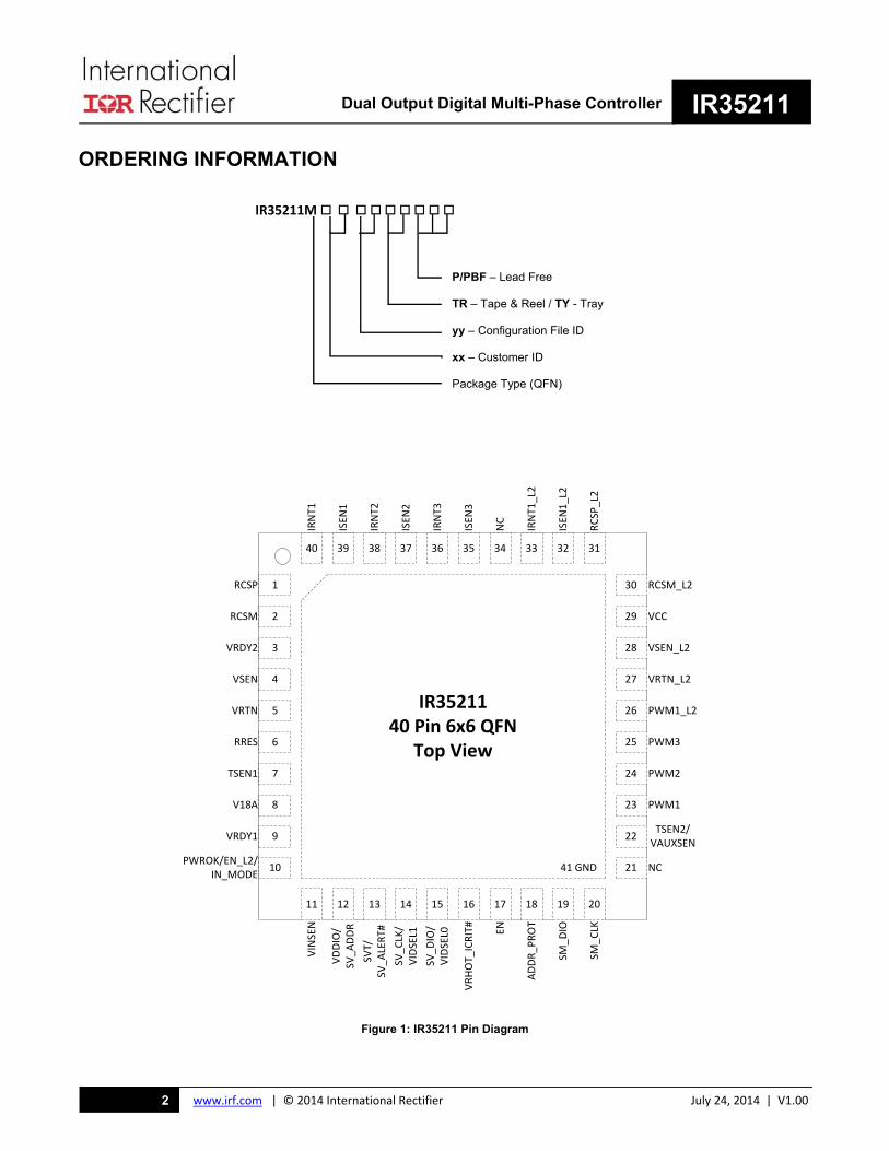
ORDERING INFORMATION IR35211M
IR3521140 Pin 6x6 QFN
Top View
1
40
2
3
4
5
6
7
10
8
9
30
29
28
27
26
25
24
21
23
22
39 38 37 36 35 34 33 32 31
11 12 13 14 15 16 17 18 19 20
41 GND
RCSP
RCSM
VRDY2
VSEN
VRTN
RRES
TSEN1
V18A
VRDY1
PWROK/EN_L2/IN_MODE
VINSEN
VDDIO/
SV_A
DDR
SVT/
SV_A
LERT#
SV_C
LK/
VIDSEL1
SV_D
IO/
VIDSEL0
VRHOT_ICRIT#
EN
ADDR_P
ROT
SM_DIO
SM_C
LK
NC
TSEN2/VAUXSEN
PWM1
PWM2
PWM3
PWM1_L2
VRTN_L2
VSEN_L2
VCC
RCSP_L2
RCSM_L2
ISEN
1_L2
IRNT1_L2
NC
ISEN
1
IRNT1
ISEN
2
IRNT2
ISEN
3
IRNT3
Figure 1: IR35211 Pin Diagram
P/PBF – Lead Free TR – Tape & Reel / TY - Tray yy – Configuration File ID xx – Customer ID Package Type (QFN)

Dual Output Digital Multi-Phase Controller IR35211
www.irf.com | © 2014 International Rectifier July 24, 2014 | V1.003
FUNCTIONAL BLOCK DIAGRAM
Figure 2: IR35211 Block Diagram
Dual Output Digital Multi-Phase Controller IR35211
www.irf.com | © 2014 International Rectifier July 24, 2014 | V1.004
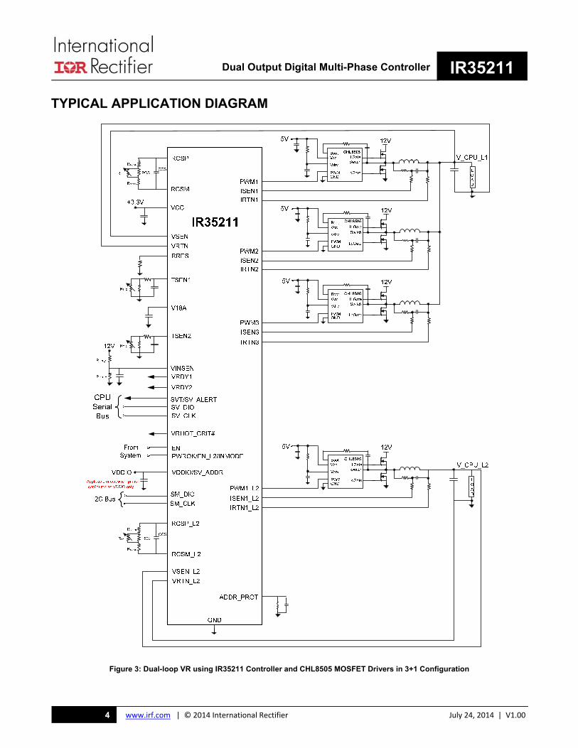
TYPICAL APPLICATION DIAGRAM
Figure 3: Dual-loop VR using IR35211 Controller and CHL8505 MOSFET Drivers in 3+1 Configuration

Dual Output Digital Multi-Phase Controller IR35211
www.irf.com | © 2014 International Rectifier July 24, 2014 | V1.005
PIN DESCRIPTIONS
PIN# PIN NAME TYPE PIN DESCRIPTION
1 RCSP A [O] Resistor Current Sense Positive Loop#1. This pin is connected to an external network to set the load line slope, bandwidth and temperature compensation for Loop #1.
2 RCSM A [O] Resistor Current Sense Minus Loop#1. This pin is connected to an external network to set the load line slope, bandwidth and temperature compensation for Loop #1.
3 VRDY2 D [O] Voltage Regulator Ready Output (Loop #2). Open-drain output that asserts high when the VR has completed soft-start to Loop #2 boot voltage. It is pulled up to an external voltage rail through and external resistor.
4 VSEN A [I] Voltage Sense Input Loop#1. This pin is connected directly to the VR output voltage of Loop #1 at the load and should be routed differentially with VRTN.
5 VRTN A [I] Voltage Sense Return Input Loop#1. This pin is connected directly to Loop#1 ground at the load and should be routed differentially with VSEN.
6 RRES A [B] Current Reference Resistor. A 1% 7.5kohm resistor is connected to this pin to set an internal precision current reference.
7 TSEN1 A [I] NTC Temperature Sense Input Loop #1. An NTC network is connected to this pin to measure temperature for VRHOT. Refer to page 44 for details.
8 V18A A [O] 1.8V Decoupling. A capacitor on this pin provides decoupling for the internal 1.8V supply.
9 VRDY1 D [O] Voltage Regulator Ready Output (Loop #1). Open-drain output that asserts high when the VR has completed soft-start to Loop #1 boot voltage. It is pulled up to an external voltage rail through and external resistor.
10
PWROK/
EN_L2/
INMODE
D [I]
Power OK Input (AMD). An input that when low indicates to return to the Boot voltage and when high indicates to use the SVI bus to set the the output voltage.
VR Enable for Loop 2. When configured, ENABLE for Loop 2 is an active high system input to power-on Loop 2, provided Vin and Vcc are present. ENABLE is not pulled up on the controller. When ENABLE is pulled low, the controller de-asserts VR READY2 and shuts down loop 2 only.
Intel Mode Pin. If configured this pin will select whether the controller is in VR12 or VR12.5 Mode. If pulled low (Logic 0) the controller will operate in VR12.5 mode, if pulled high (Logic 1) the controller will operate in VR12 mode.
11 VINSEN A [I] Voltage Sense Input. This is used to detect and measure a valid input supply voltage (typically 5V-19V) to the VR. Refer to page 16 for details.
12 VDDIO/
SV_ADDR
A [P]/
D [I]
VDDIO Input (AMD). This pin provides the voltage to which the SVT line and the SVD Acknowledge are driven high.
SVID Address Input (INTEL). A resistor to ground on this pin defines the SVID address which is latched when Vcc becomes valid. Requires a 0.01µF bypass capacitors to GND.
13 SVT/
SV_ALERT# D [O]
SVI Telemetry Output (AMD). Telemetry and VOTF information output by the IR35211.
Serial VID ALERT# (INTEL). SVID ALERT# is pulled low by the controller to alert the CPU of new VR12/12.5 Status.
14 SV_CLK/
VIDSEL1 D [I]
Serial VID Clock Input. Clock input driven by the CPU Master.
Parallel VID Selection. When configured in GPU parallel VID mode, this is pin is used to select the VID voltage registers.
15 SV_DIO/ VIDSEL0
D [B]/
D [I]
Serial VID Data I/O. Is a bi-directional serial line over which the CPU Master issues commands to controller/s slave/s.
Parallel VID Selection. When configured in GPU parallel VID mode, this is pin is used to select the VID voltage registers.
16 VRHOT_ICRIT# D [O] VRHOT_ICRIT# Output. Active low alert pin that can be programmed to assert if temperature or average load current exceeds user-definable thresholds.
17 EN D [I] VR Enable Input. ENABLE is an active high system input to power-on the regulator, provided Vin and Vcc are present. ENABLE is not pulled up on the controller. When ENABLE is pulled low, the controller de-asserts VR READY and shuts down the regulator.
18 ADDR_PROT D [B] Bus Address & I2C Bus Protection. A resistor to ground on this pin defines the I2C address offset which is latched when Vcc becomes valid. Subsequently, this pin becomes a logic input to enable or disable communication on the I2C bus offset when protection is enabled.
19 SM_DIO D [B] Serial Data Line I/O. I2C/SMBus/PMBus bi-directional serial data line.
Dual Output Digital Multi-Phase Controller IR35211
www.irf.com | © 2014 International Rectifier July 24, 2014 | V1.006
20 SM_CLK D [I] Serial Clock Input. I2C/SMBus/PMBUS serial clock line. Interface is rated to 1 MHz.
21 NC Do Not Connect.
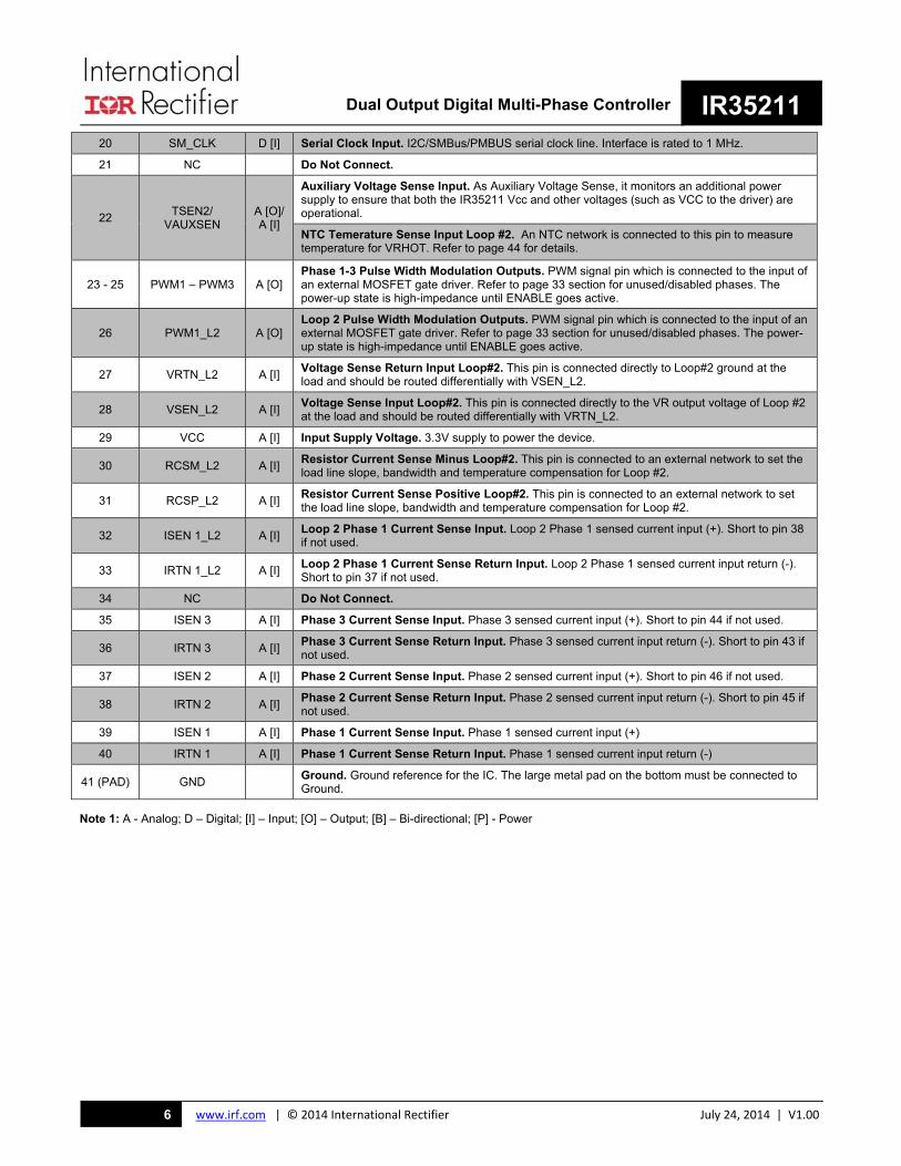
22 TSEN2/
VAUXSEN A [O]/ A [I]
Auxiliary Voltage Sense Input. As Auxiliary Voltage Sense, it monitors an additional power supply to ensure that both the IR35211 Vcc and other voltages (such as VCC to the driver) are operational.
NTC Temerature Sense Input Loop #2. An NTC network is connected to this pin to measure temperature for VRHOT. Refer to page 44 for details.
23 - 25 PWM1 – PWM3 A [O] Phase 1-3 Pulse Width Modulation Outputs. PWM signal pin which is connected to the input of an external MOSFET gate driver. Refer to page 33 section for unused/disabled phases. The power-up state is high-impedance until ENABLE goes active.
26 PWM1_L2 A [O] Loop 2 Pulse Width Modulation Outputs. PWM signal pin which is connected to the input of an external MOSFET gate driver. Refer to page 33 section for unused/disabled phases. The power-up state is high-impedance until ENABLE goes active.
27 VRTN_L2 A [I] Voltage Sense Return Input Loop#2. This pin is connected directly to Loop#2 ground at the load and should be routed differentially with VSEN_L2.
28 VSEN_L2 A [I] Voltage Sense Input Loop#2. This pin is connected directly to the VR output voltage of Loop #2 at the load and should be routed differentially with VRTN_L2.
29 VCC A [I] Input Supply Voltage. 3.3V supply to power the device.
30 RCSM_L2 A [I] Resistor Current Sense Minus Loop#2. This pin is connected to an external network to set the load line slope, bandwidth and temperature compensation for Loop #2.
31 RCSP_L2 A [I] Resistor Current Sense Positive Loop#2. This pin is connected to an external network to set the load line slope, bandwidth and temperature compensation for Loop #2.
32 ISEN 1_L2 A [I] Loop 2 Phase 1 Current Sense Input. Loop 2 Phase 1 sensed current input (+). Short to pin 38 if not used.
33 IRTN 1_L2 A [I] Loop 2 Phase 1 Current Sense Return Input. Loop 2 Phase 1 sensed current input return (-). Short to pin 37 if not used.
34 NC Do Not Connect.
35 ISEN 3 A [I] Phase 3 Current Sense Input. Phase 3 sensed current input (+). Short to pin 44 if not used.
36 IRTN 3 A [I] Phase 3 Current Sense Return Input. Phase 3 sensed current input return (-). Short to pin 43 if not used.
37 ISEN 2 A [I] Phase 2 Current Sense Input. Phase 2 sensed current input (+). Short to pin 46 if not used.
38 IRTN 2 A [I] Phase 2 Current Sense Return Input. Phase 2 sensed current input return (-). Short to pin 45 if not used.
39 ISEN 1 A [I] Phase 1 Current Sense Input. Phase 1 sensed current input (+)
40 IRTN 1 A [I] Phase 1 Current Sense Return Input. Phase 1 sensed current input return (-)
41 (PAD) GND Ground. Ground reference for the IC. The large metal pad on the bottom must be connected to Ground.
Note 1: A - Analog; D – Digital; [I] – Input; [O] – Output; [B] – Bi-directional; [P] - Power

Dual Output Digital Multi-Phase Controller IR35211
www.irf.com | © 2014 International Rectifier July 24, 2014 | V1.007
ABSOLUTE MAXIMUM RATINGS
Supply Voltage (VCC) GND-0.3V to 4.0V
RCSPx, RCSMx 0 to 2.2V
VSEN,VSEN_L2, VRTN, VRTN_L2, ISENx, IRTNx GND-0.2V to 2.7V
RRES, V18A, TSEN, TSEN2, VINSEN, VAUXSEN GND-0.2V to 2.2V
VDDIO ,SV_CLK, SV_DIO, SVT# GND-0.3V to VCC
PWMx, VIDSELx GND-0.3V to VCC
VRDY1, VRDY2, EN, PWROK, ADDR_PROT, VRHOT_ICRIT# GND-0.3V to VCC
SM_DIO, SM_CLK GND-0.3V to 5.5V
ESD Rating
Human Body Model 2000V
Machine Model 200V
Charge Device Model 1000V
Thermal Information
Thermal Resistance (θJA & θJC)1 29°C/W & 3°C/W
Maximum Operating Junction Temperature -40°C to +125°C
Maximum Storage Temperature Range -65°C to +150°C
Maximum Lead Temperature (Soldering 10s) 300°C
Note: 1. θJA is measured with the component mounted on a high effective thermal conductivity test board in free air.
Stresses beyond those listed under “Absolute Maximum Ratings” may cause permanent damage to the device. These are stress ratings only
and functional operation of the device at these or any other conditions beyond those indicated in the operational sections of the specifications
are not implied.
Dual Output Digital Multi-Phase Controller IR35211
www.irf.com | © 2014 International Rectifier July 24, 2014 | V1.008
ELECTRICAL SPECIFICATIONS
RECOMMENDED OPERATING CONDITIONS FOR RELIABLE OPERATION WITH MARGIN
Recommended Operating Ambient Temperature Range 0°C to 85°C
Supply Voltage Range +2.90V to +3.63V
The electrical characteristics table lists the spread of values guaranteed within the recommended operating conditions. Typical values represent the median values, which are related to 25°C.
ELECTRICAL CHARACTERISTICS
PARAMETER SYMBOL CONDITIONS MIN TYP MAX UNIT
Supply VCC/GND
Supply Voltage Vcc 2.90 3.3 3.63 V
Supply Current Ivcc No PWM switching 95 105 125 mA
3.3V UVLO Turn-on Threshold - 2.80 2.90 V
3.3V UVLO Turn-off Threshold 2.60 2.70 - V
Input Voltage (4V-19V) Sense Input VINSEN
Input Impedance 1 - - MΩ
Input Range V12 With 14:1 divider 0 0.857 1.1 V
UVLO Turn-on Programmable Range1
With 14:1 divider -
4.5 –15.9375
- V
UVLO Turn-off Programmable Range1
With 14:1 divider -
4.5 –15.9375
- V
OVP Threshold (if enabled)
Desktop mode 14.3 14.6 14.9 V
Notebook mode - 23.5 -
AUX Voltage (5V) Sense Input VAUXSEN
Input Impedance1 1 - - MΩ
UVLO Turn-on Threshold1 With 14:1 divider 4.3 4.5 4.75 V
UVLO Turn-off Threshold1 With 14:1 divider 3.8 4 4.3 V
Reference Voltage and DAC
Boot Voltage Range1
AMD mode -
0.00625 – 1.55
- V
Intel VR12 mode -
0.25 – 1.52
- V
Intel VR12.5 mode - 0.5 – 2.3 - V
System Accuracy3
VID = 2.005V–2.3V -1.1 - 1.1 %VID
VID = 1.0V–2.0V -0.5 - 0.5 %VID
VID = 0.8 – 0.995V -5 - 5 mV
VID = 0.25 –0.795V -8 - 8 mV
External Reference Resistor RRES 1% external bias resistor - 7.5 - kΩ
Oscillator & PWM Generator
Internal Oscillator1 - 96 - MHz
Frequency Accuracy2 -2.5 - 2.5 %
Dual Output Digital Multi-Phase Controller IR35211
www.irf.com | © 2014 International Rectifier July 24, 2014 | V1.009
PARAMETER SYMBOL CONDITIONS MIN TYP MAX UNIT
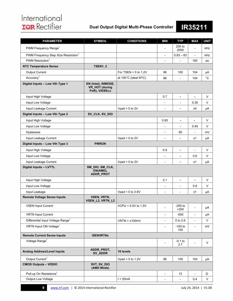
PWM Frequency Range1 - 200 to 2000
- kHz
PWM Frequency Step Size Resolution1 - 0.83 – 83 - kHz
PWM Resolution1 - - 160 ps
NTC Temperature Sense TSEN1, 2
Output Current For TSEN = 0 to 1.2V 96 100 104 µA
Accuracy1 at 100°C (ideal NTC) 96 - 104 °C
Digital Inputs – Low Vth Type 1 EN (Intel), INMODE, VR_HOT (during PoR), VIDSELx
Input High Voltage 0.7 - - V
Input Low Voltage - - 0.35 V
Input Leakage Current Vpad = 0 to 2V - - ±5 µA
Digital Inputs – Low Vth Type 2 SV_CLK, SV_DIO
Input High Voltage 0.65 - - V
Input Low Voltage - - 0.45 V
Hysteresis - 95 - mV
Input Leakage Current Vpad = 0 to 2V - - ±1 µA
Digital Inputs – Low Vth Type 3 PWROK
Input High Voltage 0.9 - - V
Input Low Voltage - - 0.6 V
Input Leakage Current Vpad = 0 to 2V - - ±1 µA
Digital Inputs – LVTTL SM_DIO, SM_CLK, EN(AMD),
ADDR_PROT
Input High Voltage 2.1 - - V
Input Low Voltage - - 0.8 V
Input Leakage Vpad = 0 to 3.6V - - ±1 µA
Remote Voltage Sense Inputs VSEN, VRTN, VSEN_L2, VRTN_L2
VSEN Input Current
VCPU = 0.5V to 1.5V -
-250 to +250
- µA
VRTN Input Current - -500 - µA
Differential Input Voltage Range1 VRTN = ±100mV - 0 to 2.6 - V
VRTN Input CM Voltage1
- -100 to 100
- mV
Remote Current Sense Inputs ISEN/IRTNx
Voltage Range1 -
-0.1 to 2.7
- V
Analog Address/Level Inputs ADDR_PROT,
SV_ADDR 16 levels
Output Current1 Vpad = 0 to 1.2V 96 100 104 µA
CMOS Outputs – VDDIO SVT, SV_DIO (AMD Mode)
Pull-up On Resistance1 - 12 - Ω
Output Low Voltage I = 20mA - - 0.4 V

Dual Output Digital Multi-Phase Controller IR35211
www.irf.com | © 2014 International Rectifier July 24, 2014 | V1.0010
PARAMETER SYMBOL CONDITIONS MIN TYP MAX UNIT
Open-Drain Outputs – 4mA Drive VRDY1, VRDY2, SM_DIO
Output Low Voltage 4mA - - 0.3 V
Output Leakage Vpad = 0 to 3.6V - - ±5 µA
Open-Drain Outputs – 20mA Drive VR_HOT_ICRIT#, SV_DIO (INTEL),
SV_ALERT
Output Low Voltage1 I = 20mA - - 0.26 V
On Resistance1 I = 20mA 7 9 13 Ω
Tri-State Leakage Ileak Vpad = 0 to 3.6V - - ±5 µA
PWM I/O PWMx
Output Low Voltage (Tri-state mode) I = -4mA - - 0.4 V
Output High Voltage (Tri-State mode) I =+4mA 2.9 - - V
Output Low Voltage (IR ATL mode) I = -4mA - - 0.4 V
Output High Voltage (IR ATL mode) I = +4mA 1.4 - 2 V
Active Tri-State Level (IR ATL mode) I = +4mA 2.9 - - V
Tri-State Leakage ATS_EN = 0, Vpad = 0 to Vcc
- - ±1 µA
PWM Auto-Detect Inputs (when 3.3V Vcc is applied) – if enabled
Input Voltage High 1.3 - - V
Input Voltage Low - - 0.5 V
I2C/PMBus & Reporting
Bus Speed1
Normal - 100 - kHz
Fast - 400 - kHz
Max Speed - 1000 - kHz
Iout & Vout Filter1 Selectable - 3.2 or 52 - Hz
Iout & Vout Update Rate1 - 20.8 - kHz
Vin & Temperature Filter1 Selectable - 3.2 or 52 - Hz
Vin & Temperature Update Rate1 - 20.8 - kHz
Vin Range Reporting1
With 14:1 divider - 0 to 15 - V
With 22:1 divider - 0 to 25 -
Vin Accuracy Reporting With 1% resistors -2 - +2 %
Vin Resolution Reporting1 - 62.5 - mV
Vout Range Reporting1 - - 2.2 V
Vout Accuracy Reporting1 No load-line - ±0.5 - %
Vout Resolution Reporting1 Vout < 2V - 7.8 - mV
Iout Per Phase Range Reporting1 0 - 62 A
Iout Accuracy Reporting1
Maximum load, all phase active (based on DCR, NTC and # active phases)
- ±2 - %
Iout Resolution Reporting1
Iout < 256A, Loop 1 - 0.5 - A
Iout < 256A, Loop 2 - 0.25 -
Temperature Range Reporting1 Loop 1, Loop 2 0 - 135 °C
Temperature Accuracy Reporting1 At 100°C, with ideal NTC -3 - 3 %
Temperature Resolution Reporting1 - 1 - °C

Dual Output Digital Multi-Phase Controller IR35211
www.irf.com | © 2014 International Rectifier July 24, 2014 | V1.0011
PARAMETER SYMBOL CONDITIONS MIN TYP MAX UNIT
Fault Protection
OVP Threshold During Start-up (until output reaches 1V)
1.2 1.275 1.35 V
OVP Operating Threshold1 (programmable)
Relative to VID - 150 to
500 - mV
Output UVP Threshold1 (programmable) Relative to VID -
-150 to -500
- mV
OVP/UVP Filter Delay1 - 160 - ns
Fast OCP Range (per phase)1 - 0 to 62 - A
Fast OCP Filter Bandwidth1 - 60 - kHz
Slow OCP Filter Bandwidth1 - 3.2/52 - Hz
OCP System Accuracy1
System excluding DCR/sense resistor
- ±2 - %
VR_HOT Range1 - 64 to 127 - °C
OTP Range1
VR_HOT level + OTP Range
- 64 to 134 - °C
Dynamic Phase Control
Current Filter Bandwidth1 For Phase drop - 5.3 - kHz
Timing Information
Automatic Configuration from MTP1 t3-t2
3.3V ready to end of configuration
- - 1 ms
Automatic Trim Time1 t4-t3 - - 4 ms
EN Delay (to ramp start) 1 - 3 - µs
VID Delay (to ramp start) 1 Loop bandwidth dependent - 5 - µs
VRDY1/2 Delay1 After reaching Boot voltage - 20 - µs
Notes: 1 Guaranteed by design. 2 PWM operating frequency will vary slightly as the number of phases changes (increases/decreases) because of the internal calculation involved in dividing a switching period evenly into the number of active phases. 3 System accuracy is for a temperature range of 0°C to +85°C. Accuracies will derate by a factor of 1.5x for temperatures outside the 0°C to +85°C range.

Dual Output Digital Multi-Phase Controller IR35211
www.irf.com | © 2014 International Rectifier July 24, 2014 | V1.0012
GENERAL DESCRIPTION
The IR35211 is a flexible, dual-loop, digital multiphase PWM buck controller optimized to convert a 12V input supply to the core voltage required by Intel and AMD high performance microprocessors and DDR memory. It is easily configurable for 1-3 phase operation on Loop #1 and 0-1 phase operation on Loop #2.
The unique partitioning of analog and digital circuits within the IR35211 provides the user with easy configuration capability while maintaining the required accuracy and performance. Access to on-chip Multiple Time Programming memory (MTP) to store the IR35211 configuration parameters enables power supply designers to optimize their designs without changing external components.
The IR35211 controls two independent output voltages. Each voltage is controlled in an identical fashion, so that the user can configure and optimize each control loop individually. Unless otherwise described, the following functions are performed on the IR35211 on each control loop independently.
OPERATING MODES
The IR35211 can be used for Intel VR12/12.5, AMD SVI1/SVI2, DDR Memory and GPU designs without significant changes to the external components (Bill of Materials). The required mode is selected in MTP and the pin-out, VID table and relevant functions are automatically configured. This greatly reduces time-to-market and eliminates the need to manage and inventory 6 different PWM controllers.
DIGITAL CONTROLLER & PWM
A linear Proportional-Integral-Derivative (PID) digital controller provides the loop compensation for system regulation. The digitized error voltage from the high-speed voltage error ADC is processed by the digital compensator. The digital PWM generator uses the outputs of the PID and the phase current balance control signals to determine the pulse width for each phase on each loop. The PWM generator has enough resolution to ensure that there are no limit cycles. The compensator coefficients are user configurable to enable optimized system response. The compen-sation algorithm uses a PID with two additional programmable poles. This provides the digital equivalent of a Type III analog compensator.
ADAPTIVE TRANSIENT ALGORITHM (ATA)
Dynamic load step-up and load step-down transients require fast system response to maintain the output voltage within specification limits. This is achieved by a unique adaptive non-linear digital transient control loop based on a proprietary algorithm.
MULTIPLE TIME PROGRAMMING MEMORY
The multiple time programming memory (MTP) stores the device configuration. At power-up, MTP contents are transferred to operating registers for access during device operation. MTP allows customization during both design and high-volume manufacturing. MTP integrity is verified by cyclic redundancy code (CRC) checking on each power up. The controller will not start in the event of a CRC error.
The IR35211 offers up to 8 writes to configure basic device parameters such as frequency, fault operation characteristics, and boot voltage. This represents a significant size and component saving compared to traditional analog methods. The following pseudo-code illustrates how to write the MTP:
# write data Set MTP Command Register = WRITE, Line Pointer = An unused line Poll MTP Command Register until Operation = IDLE.
# verify data was written correctly Issue a READ Command; then poll OTP Operation Register till Operation = IDLE Verify that the Read Succeeded
INTERNAL OSCILLATOR
The IR35211 has a single 96MHz internal oscillator that generates all the internal system clock frequencies required for proper device function. The oscillator frequency is factory trimmed for precision and has extremely low jitter (Figure 4) even in light-load mode (Figure 5). The single internal oscillator is used to set the same switching frequency on each loop.

Dual Output Digital Multi-Phase Controller IR35211
www.irf.com | © 2014 International Rectifier July 24, 2014 | V1.0013
Figure 4: Persistence plot of a 3Φ, 50A system
Figure 5: Persistence plot in 1Φ, 10A
HIGH-PRECISION VOLTAGE REFERENCE
The internal high-precision voltage reference supplies the required reference voltages to the VID DACs, ADCs and other analog circuits. This factory trimmed reference is guaranteed over temperature and manufacturing variations.
HIGH PRECISION CURRENT REFERENCE
An on-chip precision current reference is derived using an off-chip precision resistor connected to the RRES pin of the IR35211. RRES must be a 7.5kΩ, 1% tolerance resistor, placed very close to the controller pin to minimize parasitics.
VOLTAGE SENSE
An error voltage is generated from the difference between the target voltage, defined by the VID and load line (if implemented), and the differential, remotely sensed, output voltage. For each loop, the error voltage is digitized by a high-speed, high-precision ADC. An anti-alias filter provides the necessary high frequency noise rejection. The gain
and offset of the voltage sense circuitry for each loop is factory trimmed to deliver the required accuracy.
CURRENT SENSE
Lossless inductor DCR or precision resistor current sensing is used to accurately measure individual phase currents. Using a simple off-chip thermistor, resistor and capacitor network for each loop, a thermally compensated load line is generated to meet the given power system requirement. A filtered voltage, which is a function of the total load current and the target load line resistance, is summed into each voltage sense path to accomplish the Active Voltage Positioning (AVP) function.
VID DECODER
The VID decoder receives a VID code from the CPU that is converted to an internal code representing the VID voltage. This block also outputs the signal for VR disable if a VID shutdown code has been received. The VID code is 8 bits in AMD SVI2 & Intel VR12/VR12.5 mode and 7 bits in AMD SVI1 mode.
MOSFET DRIVER, POWER STAGE AND DRMOS COMPATIBILITY
The output PWM signals of the IR35211 are designed for compatibility with the CHL85xx family of active tri-level (ATL) MOSFET drivers. CHL85xx drivers have a fast disable capability which enables any phase to be turned off on-the-fly. It supports power-saving control modes, improved transient response, and superior on the fly phase dropping without having to route multiple output disable (ODB or SMOD) signals.
In addition, the IR35211 provides the flexibility to configure PWM levels to operate with external MOSFET drivers, Power Stages or driver-MOSFET (DrMOS) devices that support Industry standard +3.3V tri-state signaling.
I2C & PMBUS INTERFACE
An I2C or PMBus interface is used to communicate with the IR35211. This two-wire serial interface consists of clock and data signals and operates as fast as 1MHz. The bus provides read and write access to the internal registers for configuration and monitoring of operating parameters and can also be used to program on-chip non-volatile memory (MTP) to store operating parameters.
PWM1
PWM1
PWM2
PWM3
Vdd
Vdd

Dual Output Digital Multi-Phase Controller IR35211
www.irf.com | © 2014 International Rectifier July 24, 2014 | V1.0014
To ensure operation with multiple devices on the bus, an exclusive address for the IR35211 is programmed into MTP. The IR35211, additionally, supports pin-programming of the address.
To protect customer configuration and information, the I2C interface can be completely locked to provide no access or configured for limited access with a 16-bit software password. Limited access includes both write and read protection options. In addition, there is a telemetry only mode which allows reads from the telemetry registers only.
The IR35211 provides a hardware pin security option to provide extra protection. The protect pin is shared with the ADDR pin and is automatically engaged once the address is read. The pin must be driven high to disable protection. The pin can be enabled or disabled by a configuration setting in MTP.
The IR35211 supports the packet error checking (PEC) protocol and a number of PMBus commands to monitor voltages and currents. Refer to the PMBus Command Codes in Table 63.
IR DIGITAL POWER DESIGN CENTER (DPDC)
GUI
The IR DPDC GUI provides the designer with a comprehensive design environment that includes screens to calculate VR efficiency and DC error budget, design the thermal compensation networks and feedback loops, and produce calculated Bode plots and output impedance plots. The DPDC environment is a key utility for design optimization, debug, and validation of designs that save designer significant time, allowing faster time-to-market (TTM).
The DPDC also allows real-time design optimization and real-time monitoring of key parameters such as output current and power, input current and power, efficiency, phase currents, temperature, and faults.
The IR DPDC GUI allows access to the system configuration settings for switching frequency, MOSFET driver compatibility, soft start rate, VID table, PSI, loop compensation, transient control system parameters, input under-voltage, output over-voltage, output under-voltage, output over-current and over-temperature.
PROGRAMMING
Once a design is complete, the DPDC produces a complete configuration file.
The configuration file can be re-coded into an I2C/PMBus master (e.g. a Test System) and loaded into the IR35211 using the bus protocols described on page 50. The IR35211 has a special in-circuit programming mode that allows the MTP to be loaded at board test in mass production without powering on the entire board.
REAL-TIME MONITORING
The IR35211 can be accessed through the use of PMBus Command codes (described in Table 63) to read the real time status of the VR system including input voltage, output voltage, input and output current, input and output power, efficiency, and temperature.

Dual Output Digital Multi-Phase Controller IR35211
www.irf.com | © 2014 International Rectifier July 24, 2014 | V1.0015
THEORY OF OPERATION OPERATING MODE
The IR35211 changes its pin-out and functionality based on the user-selected operating mode, allowing one device to be used for multiple applications without significant BoM changes. This greatly reduces the user’s design cycles and TTM.
The functionality for each operating mode is completely configurable by simple selections in MTP. The mode configuration is shown in Table 1.
TABLE 1: MODE SELECTION
Mode Description
VR12 Intel® VR12 (Selected via MTP or external INMODE pin pulled high).
VR12.5 Intel® VR12.5 (Selected via MTP or external INMODE pin pulled low).
Memory Intel® VR12 compliant memory VR with Loop 2 output voltage ½ Loop 1 output voltage.
SVI2.0 AMD® SVI2.0 (Selected via MTP or external SVT pin).
SVI1.0 AMD® SVI1.0 (Selected via MTP or external SVT pin).
GPU Parallel GPU VR with external VID select pins.
GPU Serial GPU VR with Serial VID interface.
DEVICE POWER-ON AND INITIALIZATION
The IR35211 is powered from a 3.3V DC supply. Figure 6 shows the timing diagram during device initialization. An internal LDO generates a 1.8V rail to power the control logic within the device. During initial startup, the 1.8V rail follows the rising 3.3V supply voltage, proportional to an internal resistor tree. The internal oscillator becomes active at t1 as the 1.8V rail is ramping up. Until soft-start begins, the IR35211 PWM outputs are disabled in a high impedance state to ensure that the system comes up in a known state.
The controller comes out of power-on reset (POR) at t2 when the 3.3V supply is high enough for the internal bias central to generate 1.8V. At this time, if enabled in MTP and when the VINSEN voltage is valid, the controller will detect the populated phases by sensing the voltage on the PWM pins. If the voltage is less than the Auto Phase Detect threshold (unused PWMs are grounded), the controller assumes the phase is
unpopulated. Once the phase detection is complete the contents of the MTP are transferred to the registers by time t3 and the automatic trim routines are complete by time t4. The register settings and number of phases define the controller performance specific to the VR configuration - including trim settings, soft start ramp rate, boot voltage and PWM signal compatibility with the MOSFET driver.
Figure 6: Controller Startup and Initialization
Once the registers are loaded from MTP, the designer can use I2C to re-configure the registers to suit the specific VR design requirements if desired.
TEST MODE
Driving the ENABLE and VR_HOT pins low engages a special test mode in which the I2C address changes to 0Ah. This allows individual in-circuit programming of the controller. This is specifically useful in multi-controller systems that use a single I2C bus. Note that MTP will not load to the working registers until either ENABLE or VR_HOT goes high.
SUPPLY VOLTAGE
The controller is powered by the 3.3V supply rail. Once initialization of the device is complete, steady and stable supply voltage rails and a VR Enable signal (EN) are required to set the controller into an active state. A high EN signal is required to enable the PWM signals and begin the soft start sequence after the 3.3V and VIN supply rails are determined to be within the defined operating bands. The recom-mended decoupling for the 3.3V is shown in Figure 7.
Dual Output Digital Multi-Phase Controller IR35211
www.irf.com | © 2014 International Rectifier July 24, 2014 | V1.0016
The Vcc pins should have a 0.1µF and 1µF X7R-type ceramic capacitors placed as close as possible to the package.
Figure 7: Vcc 3.3V decoupling
The V18A pin must have a 4.7µF, X5R type decoupling capacitor connected close to the package as shown in Figure 8.
Figure 8: V18A decoupling
The IR35211 is designed to accommodate a wide variety of input power supplies and applications and offers programmability of the VINSEN turn-on/off voltages.
TABLE 2: VINSEN TURN-ON/OFF VOLTAGE RANGE
Threshold Range
Turn-on 4.5V to 15.9375V in 1/16V steps1
Turn-off 4.5V to 15.9375V in 1/16V steps1 1 Must not be programmed below 4.5V
The supply voltage on the VINSEN pin is compared against a programmable threshold. Once the rising VINSEN voltage crosses the turn-on threshold, EN is asserted and all PWM outputs become active. The VINSEN supply voltage is valid until it declines below its programmed turn-off level.
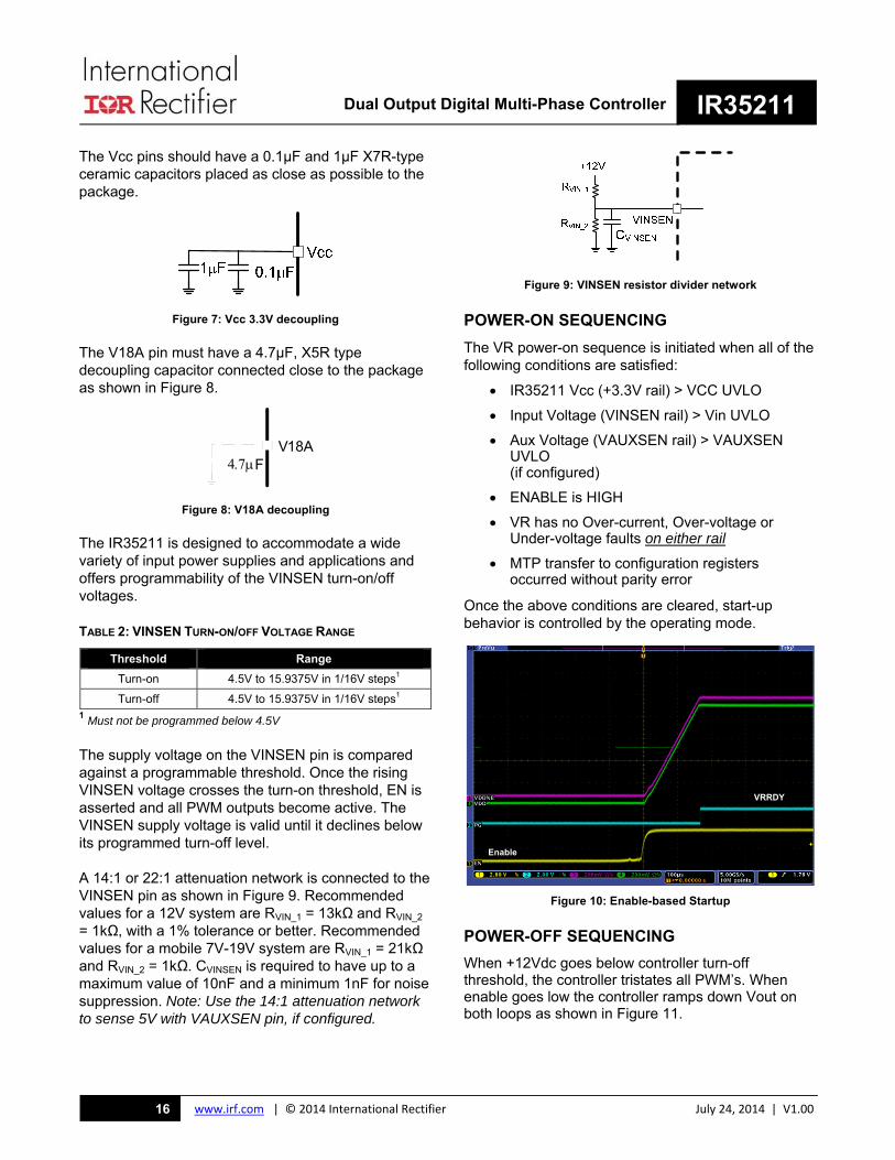
A 14:1 or 22:1 attenuation network is connected to the VINSEN pin as shown in Figure 9. Recommended values for a 12V system are RVIN_1 = 13kΩ and RVIN_2 = 1kΩ, with a 1% tolerance or better. Recommended values for a mobile 7V-19V system are RVIN_1 = 21kΩ and RVIN_2 = 1kΩ. CVINSEN is required to have up to a maximum value of 10nF and a minimum 1nF for noise suppression. Note: Use the 14:1 attenuation network to sense 5V with VAUXSEN pin, if configured.
Figure 9: VINSEN resistor divider network
POWER-ON SEQUENCING
The VR power-on sequence is initiated when all of the following conditions are satisfied:
IR35211 Vcc (+3.3V rail) > VCC UVLO
Input Voltage (VINSEN rail) > Vin UVLO
Aux Voltage (VAUXSEN rail) > VAUXSEN UVLO (if configured)
ENABLE is HIGH
VR has no Over-current, Over-voltage or Under-voltage faults on either rail
MTP transfer to configuration registers occurred without parity error
Once the above conditions are cleared, start-up behavior is controlled by the operating mode.
Figure 10: Enable-based Startup
POWER-OFF SEQUENCING
When +12Vdc goes below controller turn-off threshold, the controller tristates all PWM’s. When enable goes low the controller ramps down Vout on both loops as shown in Figure 11.
V18 A F
VRRDY
Enable
Dual Output Digital Multi-Phase Controller IR35211
www.irf.com | © 2014 International Rectifier July 24, 2014 | V1.0017
Figure 11: Enable-based Shutdown
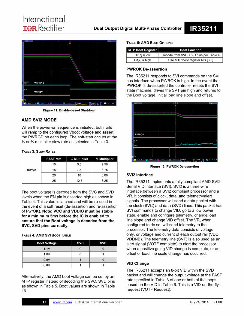
AMD SVI2 MODE
When the power-on sequence is initiated, both rails will ramp to the configured Vboot voltage and assert the PWRGD on each loop. The soft-start occurs at the ½ or ¼ multiplier slew rate as selected in Table 3.
TABLE 3: SLEW RATES
mV/µs
FAST rate ½ Multiplier ¼ Multiplier
10 5.0 2.50
15 7.5 3.75
20 10 5.00
25 12.5 6.25
The boot voltage is decoded from the SVC and SVD levels when the EN pin is asserted high as shown in Table 4. This value is latched and will be re-used in the event of a soft reset (de-assertion and re-assertion of PwrOK). Note: VCC and VDDIO must be stable for a minimum 5ms before the IC is enabled to ensure that the Boot voltage is decoded from the SVC, SVD pins correctly.
TABLE 4: AMD SVI BOOT TABLE
Boot Voltage SVC SVD
1.1V 0 0
1.0V 0 1
0.9V 1 0
0.8V 1 1
Alternatively, the AMD boot voltage can be set by an MTP register instead of decoding the SVC, SVD pins as shown in Table 5. Boot values are shown in Table 16.
TABLE 5: AMD BOOT OPTIONS
MTP Boot Register Boot Location
Bit[7] = low Decode from SVC, SVD pins per Table 4
Bit[7] = high Use MTP boot register bits [6:0]
PWROK De-assertion
The IR35211 responds to SVI commands on the SVI bus interface when PWROK is high. In the event that PWROK is de-asserted the controller resets the SVI state machine, drives the SVT pin high and returns to the Boot voltage, initial load line slope and offset.
Figure 12: PWROK De-assertion
SVI2 Interface
The IR35211 implements a fully compliant AMD SVI2 Serial VID interface (SVI). SVI2 is a three-wire interface between a SVI2 compliant processor and a VR. It consists of clock, data, and telemetry/alert signals. The processor will send a data packet with the clock (SVC) and data (SVD) lines. This packet has SVI commands to change VID, go to a low power state, enable and configure telemetry, change load line slope and change VID offset. The VR, when configured to do so, will send telemetry to the processor. The telemetry data consists of voltage only, or voltage and current of each output rail (VDD, VDDNB). The telemetry line (SVT) is also used as an alert signal (VOTF complete) to alert the processor when a positive going VID change is complete, or an offset or load line scale change has occurred.
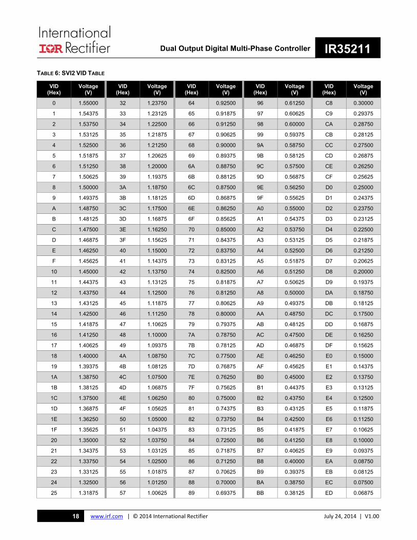
VID Change
The IR35211 accepts an 8-bit VID within the SVD packet and will change the output voltage at the FAST rate specified in Table 3 of one or both of the loops based on the VID in Table 6. This is a VID-on-the-fly-request (VOTF Request).
VRRDY
VRRDY2
PWROK
Dual Output Digital Multi-Phase Controller IR35211
www.irf.com | © 2014 International Rectifier July 24, 2014 | V1.0018
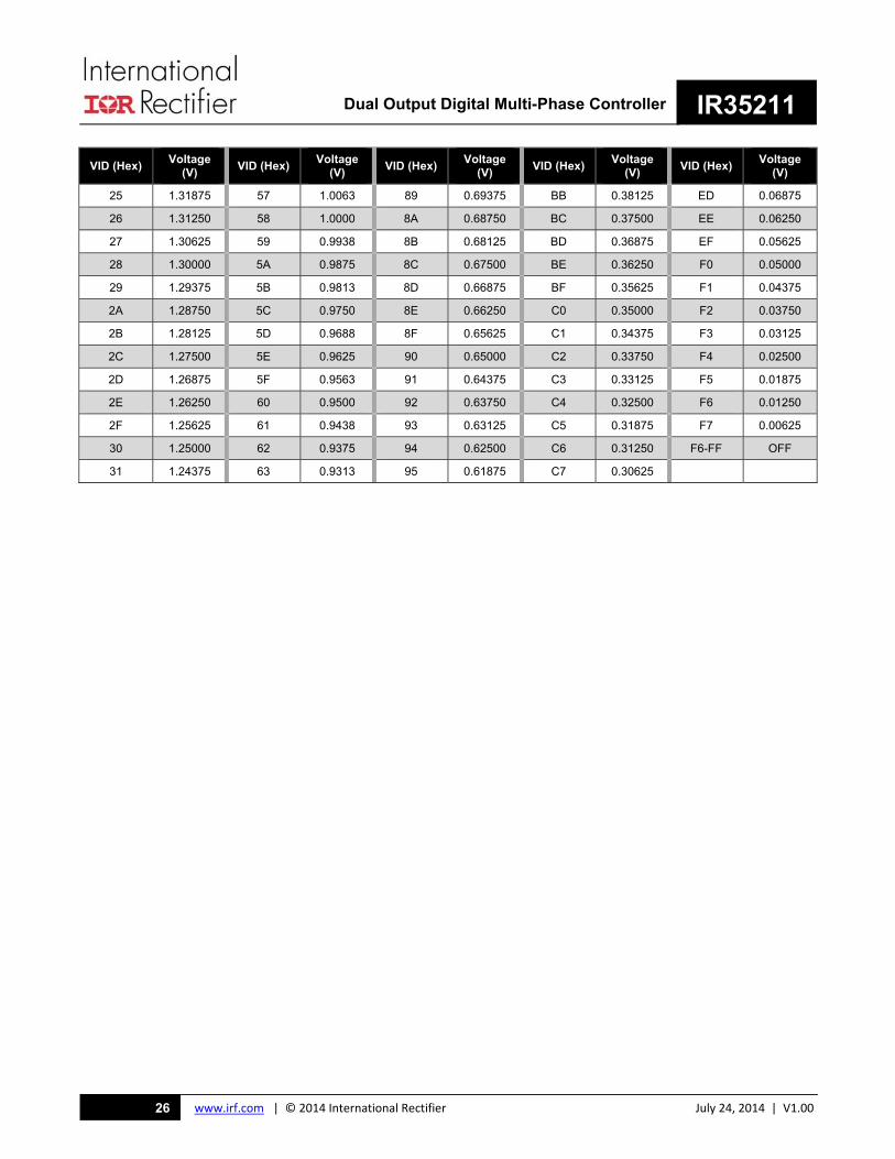
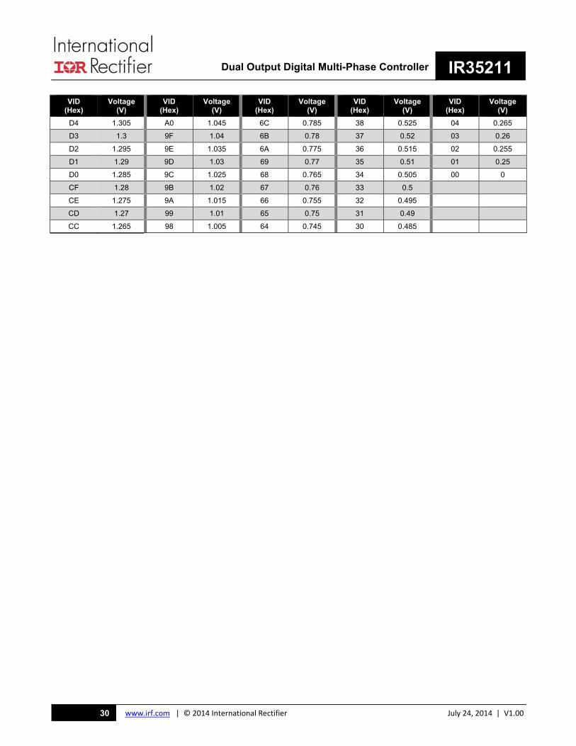
TABLE 6: SVI2 VID TABLE
VID (Hex)
Voltage (V)
VID (Hex)
Voltage (V)
VID (Hex)
Voltage (V)
VID (Hex)
Voltage (V)
VID (Hex)
Voltage (V)
0 1.55000 32 1.23750 64 0.92500 96 0.61250 C8 0.30000
1 1.54375 33 1.23125 65 0.91875 97 0.60625 C9 0.29375
2 1.53750 34 1.22500 66 0.91250 98 0.60000 CA 0.28750
3 1.53125 35 1.21875 67 0.90625 99 0.59375 CB 0.28125
4 1.52500 36 1.21250 68 0.90000 9A 0.58750 CC 0.27500
5 1.51875 37 1.20625 69 0.89375 9B 0.58125 CD 0.26875
6 1.51250 38 1.20000 6A 0.88750 9C 0.57500 CE 0.26250
7 1.50625 39 1.19375 6B 0.88125 9D 0.56875 CF 0.25625
8 1.50000 3A 1.18750 6C 0.87500 9E 0.56250 D0 0.25000
9 1.49375 3B 1.18125 6D 0.86875 9F 0.55625 D1 0.24375
A 1.48750 3C 1.17500 6E 0.86250 A0 0.55000 D2 0.23750
B 1.48125 3D 1.16875 6F 0.85625 A1 0.54375 D3 0.23125
C 1.47500 3E 1.16250 70 0.85000 A2 0.53750 D4 0.22500
D 1.46875 3F 1.15625 71 0.84375 A3 0.53125 D5 0.21875
E 1.46250 40 1.15000 72 0.83750 A4 0.52500 D6 0.21250
F 1.45625 41 1.14375 73 0.83125 A5 0.51875 D7 0.20625
10 1.45000 42 1.13750 74 0.82500 A6 0.51250 D8 0.20000
11 1.44375 43 1.13125 75 0.81875 A7 0.50625 D9 0.19375
12 1.43750 44 1.12500 76 0.81250 A8 0.50000 DA 0.18750
13 1.43125 45 1.11875 77 0.80625 A9 0.49375 DB 0.18125
14 1.42500 46 1.11250 78 0.80000 AA 0.48750 DC 0.17500
15 1.41875 47 1.10625 79 0.79375 AB 0.48125 DD 0.16875
16 1.41250 48 1.10000 7A 0.78750 AC 0.47500 DE 0.16250
17 1.40625 49 1.09375 7B 0.78125 AD 0.46875 DF 0.15625
18 1.40000 4A 1.08750 7C 0.77500 AE 0.46250 E0 0.15000
19 1.39375 4B 1.08125 7D 0.76875 AF 0.45625 E1 0.14375
1A 1.38750 4C 1.07500 7E 0.76250 B0 0.45000 E2 0.13750
1B 1.38125 4D 1.06875 7F 0.75625 B1 0.44375 E3 0.13125
1C 1.37500 4E 1.06250 80 0.75000 B2 0.43750 E4 0.12500
1D 1.36875 4F 1.05625 81 0.74375 B3 0.43125 E5 0.11875
1E 1.36250 50 1.05000 82 0.73750 B4 0.42500 E6 0.11250
1F 1.35625 51 1.04375 83 0.73125 B5 0.41875 E7 0.10625
20 1.35000 52 1.03750 84 0.72500 B6 0.41250 E8 0.10000
21 1.34375 53 1.03125 85 0.71875 B7 0.40625 E9 0.09375
22 1.33750 54 1.02500 86 0.71250 B8 0.40000 EA 0.08750
23 1.33125 55 1.01875 87 0.70625 B9 0.39375 EB 0.08125
24 1.32500 56 1.01250 88 0.70000 BA 0.38750 EC 0.07500
25 1.31875 57 1.00625 89 0.69375 BB 0.38125 ED 0.06875

Dual Output Digital Multi-Phase Controller IR35211
www.irf.com | © 2014 International Rectifier July 24, 2014 | V1.0019
VID (Hex)
Voltage (V)
VID (Hex)
Voltage (V)
VID (Hex)
Voltage (V)
VID (Hex)
Voltage (V)
VID (Hex)
Voltage (V)
26 1.31250 58 1.00000 8A 0.68750 BC 0.37500 EE 0.06250
27 1.30625 59 0.99375 8B 0.68125 BD 0.36875 EF 0.05625
28 1.30000 5A 0.98750 8C 0.67500 BE 0.36250 F0 0.05000
29 1.29375 5B 0.98125 8D 0.66875 BF 0.35625 F1 0.04375
2A 1.28750 5C 0.97500 8E 0.66250 C0 0.35000 F2 0.03750
2B 1.28125 5D 0.96875 8F 0.65625 C1 0.34375 F3 0.03125
2C 1.27500 5E 0.96250 90 0.65000 C2 0.33750 F4 0.02500
2D 1.26875 5F 0.95625 91 0.64375 C3 0.33125 F5 0.01875
2E 1.26250 60 0.95000 92 0.63750 C4 0.32500 F6 0.01250
2F 1.25625 61 0.94375 93 0.63125 C5 0.31875 F7 0.00625
30 1.25000 62 0.93750 94 0.62500 C6 0.31250 F6-FF OFF
31 1.24375 63 0.93125 95 0.61875 C7 0.30625

Dual Output Digital Multi-Phase Controller IR35211
www.irf.com | © 2014 International Rectifier July 24, 2014 | V1.0020
PSI[x]_L and TFN
PSI0_L is Power State Indicator Level 0. When this bit is asserted the IR35211 will drop to 1 phase. This will only occur if the output current is low enough (typically <20A) to enter PSI0, else the VR will remain in full phase operation.
PSI1_L is Power State Indicator Level 1. When this bit is asserted along with the PSI0_L bit, the IR35211 will enter diode emulation mode. This will only occur if the output current is low enough (typically <5A) to enter PSI1, else the VR will enter PSI0_L mode of operation.
TFN is an active high signal that allows the processor to control the telemetry functionality of the VR. If TFN=1, then the VR telemetry will be configured per Table 7.
TABLE 7: TFN TRUTH TABLE
VDD, VDDNB Domain Selector bit
Meaning
0, 0 Telemetry is in voltage only mode.
0, 1 Telemetry is in voltage
& current mode.
1, 0 Telemetry is disabled.
1, 1 Reserved.
SVT Telemetry
The IR35211 has the ability to sample and report voltage and current for the VDD and VDDNB domains. The IR35211 reports this telemetry serially over the SVT wire which is clocked by the processor driven SVC. If in voltage only telemetry mode then the sampled voltage for VDD and VDDNB are sent together in every SVT telemetry packet at a rate of 20kHz. If in voltage and current mode then the sampled voltage and current for VDD is sent out in one SVT telemetry packet followed by the sampled voltage and current for VDDNB in the next SVT telemetry packet at a rate of 40kHz. The voltage and current are moving averages based on the filters and update rates specified in the Electrical Specification Table. The voltage is reported as a function of the Set VID minus Iout times the Load Line Resistance. The current is reported as a percentage of the Icc_max register, where a value of FFh represents 100% and 00h represents 0% of the Icc_max setting. Resolution of the current reporting is 0.39% (1/256).
Load Line Slope Trim
The IR35211 has the ability for the processor to change the load line slope of each loop independently through the SVI2 bus while ENABLE and PWROK are asserted via the serial VID interface. The slope change applies to initial load line slope as set by the external RCSP/RCSM resistor network. The load line slope can be disabled or adjusted by -40%, -20%, 0%, +20%, +40%, +60%, or +80%.
Offset Trim
The IR35211 has the ability for the processor to change the offset of each loop independently while ENABLE and PWROK are asserted via the serial VID interface. The offset can be left unchanged, disabled, or changed +25mV or -25mV.
Ispike/Dual OCP Support
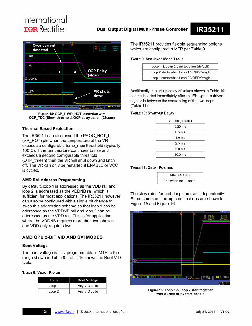
The IR35211 has two current limit thresholds. One threshold is for short duration current spikes (Fast OCP). When this threshold, typically a percentage above the peak processor current, is exceeded the VR quickly shuts down. The other threshold, typically a percentage above the thermal design current (TDC), is heavily filtered (Slow OCP) and shuts down the VR when the average current exceeds it. To meet AMD specifications, exceeding both thresholds will assert the OCP_L (VR_HOT) pin and delay the over-current shut down by 10usec for FAST threshold and 20usec for the SLOW threshold, typically. Figure 13 and Figure 14 show the delay action of the OCP shutdown with the OCP_L (VR_HOT) and PWRGD pins.
Figure 13: OCP_L (VR_HOT) assertion with OCP_spike (Fast) threshold. OCP delay action (11usec)
OCP Delay (fast)
Over-current detected
VR shuts down
Vdd
Idd
OCP_L
PG
Dual Output Digital Multi-Phase Controller IR35211
www.irf.com | © 2014 International Rectifier July 24, 2014 | V1.0021
Figure 14: OCP_L (VR_HOT) assertion with OCP_TDC (Slow) threshold. OCP delay action (22usec)
Thermal Based Protection
The IR35211 can also assert the PROC_HOT_L (VR_HOT) pin when the temperature of the VR exceeds a configurable temp_max threshold (typically 100°C). If the temperature continues to rise and exceeds a second configurable threshold (OTP_thresh) then the VR will shut down and latch off. The VR can only be restarted if ENABLE or VCC is cycled.
AMD SVI Address Programming
By default, loop 1 is addressed as the VDD rail and loop 2 is addressed as the VDDNB rail which is sufficient for most applications. The IR35211 however, can also be configured with a single bit change to swap this addressing scheme so that loop 1 can be addressed as the VDDNB rail and loop 2 can be addressed as the VDD rail. This is for application where the VDDNB requires more than two phases and VDD only requires two.
AMD GPU 2-BIT VID AND SVI MODES
Boot Voltage
The boot voltage is fully programmable in MTP to the range shown in Table 8. Table 16 shows the Boot VID table.
TABLE 8: VBOOT RANGE
Loop Boot Voltage
Loop 1 Any VID code
Loop 2 Any VID code
The IR35211 provides flexible sequencing options which are configured in MTP per Table 9.
TABLE 9: SEQUENCE MODE TABLE
Loop 1 & Loop 2 start together (default)
Loop 2 starts when Loop 1 VRRDY=high
Loop 1 starts when Loop 2 VRRDY=high
Additionally, a start-up delay of values shown in Table 10 can be inserted immediately after the EN signal is driven high or in between the sequencing of the two loops (Table 11).
TABLE 10: START-UP DELAY
0.0 ms (default)
0.25 ms
0.5 ms
1.0 ms
2.5 ms
5.0 ms
10.0 ms
TABLE 11: DELAY POSITION
After ENABLE
Between the 2 loops
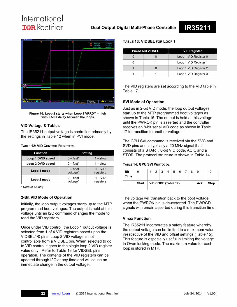
The slew rates for both loops are set independently. Some common start-up combinations are shown in Figure 15 and Figure 16.
Figure 15: Loop 1 & Loop 2 start together with 0.25ms delay from Enable
OCP Delay(slow)
Over-current detected
VR shuts down
Vdd
Idd
OCP_L
PG
Dual Output Digital Multi-Phase Controller IR35211
www.irf.com | © 2014 International Rectifier July 24, 2014 | V1.0022
Figure 16: Loop 2 starts when Loop 1 VRRDY = high with 0.5ms delay between the loops
VID Voltage & Tables
The IR35211 output voltage is controlled primarily by the settings in Table 12 when in PVI mode.
TABLE 12: VID CONTROL REGISTERS
Function Setting
Loop 1 DVID speed 0 – fast* 1 – slow
Loop 2 DVID speed 0 – fast* 1 – slow
Loop 1 mode 0 – boot voltage*
1 – VID registers
Loop 2 mode 0 – boot voltage*
1 – VID registers
* Default Setting
2-Bit VID Mode of Operation
Initially, the loop output voltages starts up to the MTP programmed boot voltages. The output is held at this voltage until an I2C command changes the mode to read the VID registers.
Once under VID control, the Loop 1 output voltage is selected from 1 of 4 VID registers based upon the VIDSEL1/0 pins. Loop 2 VID voltage is not controllable from a VIDSEL pin. When selected to go to VID control it goes to the single loop 2 VID register value only. Refer to Table 13 for VIDSEL pins operation. The contents of the VID registers can be updated through I2C at any time and will cause an immediate change in the output voltage.
TABLE 13: VIDSEL FOR LOOP 1
Pin-based VIDSEL VID Register
0 0 Loop 1 VID Register 0
0 1 Loop 1 VID Register 1
1 0 Loop 1 VID Register 2
1 1 Loop 1 VID Register 3
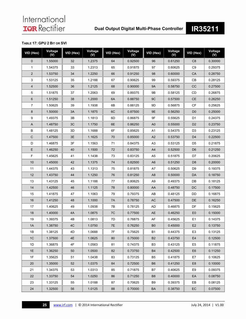
The VID registers are set according to the VID table in Table 17.
SVI Mode of Operation
Just as in 2-bit VID mode, the loop output voltages start up to the MTP programmed boot voltages as shown in Table 16. The output is held at this voltage until the PWROK pin is asserted and the controller receives an 8-bit serial VID code as shown in Table 17 to transition to another voltage.
The GPU SVI command is received via the SVC and SVD pins and is typically a 20 MHz signal that consists of a START, 8-bit VID code, ACK, and a STOP. The protocol structure is shown in Table 14.
TABLE 14: GPU SVI PROTOCOL
Bit
Time
0 1 2 3 4 5 6 7 8 9 10
Start VID CODE (Table 17) Ack Stop
The voltage will transition back to the boot voltage when the PWROK pin is de-asserted. The PWRGD signals will remain asserted during this transition time.
Vmax Function
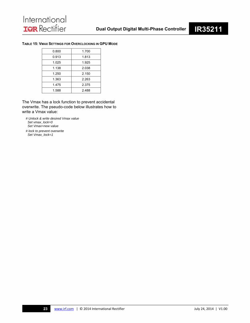
The IR35211 incorporates a safety feature whereby the output voltage can be limited to a maximum value irrespective of the VID and offset settings (Table 15). This feature is especially useful in limiting the voltage in Overclocking mode. The maximum value for each loop is stored in MTP.
Dual Output Digital Multi-Phase Controller IR35211
www.irf.com | © 2014 International Rectifier July 24, 2014 | V1.0023
TABLE 15: VMAX SETTINGS FOR OVERCLOCKING IN GPU MODE
0.800 1.700
0.913 1.813
1.025 1.925
1.138 2.038
1.250 2.150
1.363 2.263
1.475 2.375
1.588 2.488
The Vmax has a lock function to prevent accidental overwrite. The pseudo-code below illustrates how to write a Vmax value:
# Unlock & write desired Vmax value Set vmax_lock=0 Set Vmax=new value
# lock to prevent overwrite Set Vmax_lock=1

Dual Output Digital Multi-Phase Controller IR35211
www.irf.com | © 2014 International Rectifier July 24, 2014 | V1.0024
TABLE 16: AMD BOOT VOLTAGE
VID (Hex) Voltage (V) VID (Hex) Voltage (V) VID (Hex) Voltage (V) VID (Hex) Voltage (V)
80 1.5500 A0 1.1500 C0 0.7500 E0 0.3500
81 1.5375 A1 1.1375 C1 0.7375 E1 0.3375
82 1.5250 A2 1.1250 C2 0.7250 E2 0.3250
83 1.5125 A3 1.1125 C3 0.7125 E3 0.3125
84 1.5000 A4 1.1000 C4 0.7000 E4 0.3000
85 1.4875 A5 1.0875 C5 0.6875 E5 0.2875
86 1.4750 A6 1.0750 C6 0.6750 E6 0.2750
87 1.4625 A7 1.0625 C7 0.6625 E7 0.2625
88 1.4500 A8 1.0500 C8 0.6500 E8 0.2500
89 1.4375 A9 1.0375 C9 0.6375 E9 0.2375
8A 1.4250 AA 1.0250 CA 0.6250 EA 0.2250
8B 1.4125 AB 1.0125 CB 0.6125 EB 0.2125
8C 1.4000 AC 1.0000 CC 0.6000 EC 0.2000
8D 1.3875 AD 0.9875 CD 0.5875 ED 0.1875
8E 1.3750 AE 0.9750 CE 0.5750 EE 0.1750
8F 1.3625 AF 0.9625 CF 0.5625 EF 0.1625
90 1.3500 B0 0.9500 D0 0.5500 F0 0.1500
91 1.3375 B1 0.9375 D1 0.5375 F1 0.1375
92 1.3250 B2 0.9250 D2 0.5250 F2 0.1250
93 1.3125 B3 0.9125 D3 0.5125 F3 0.1125
94 1.3000 B4 0.9000 D4 0.5000 F4 0.1000
95 1.2875 B5 0.8875 D5 0.4875 F5 0.0875
96 1.2750 B6 0.8750 D6 0.4750 F6 0.0750
97 1.2625 B7 0.8625 D7 0.4625 F7 0.0625
98 1.2500 B8 0.8500 D8 0.4500 F8 0.0500
99 1.2375 B9 0.8375 D9 0.4375 F9 0.0375
9A 1.2250 BA 0.8250 DA 0.4250 FA 0.0250
9B 1.2125 BB 0.8125 DB 0.4125 FB OFF
9C 1.2000 BC 0.8000 DC 0.4000 FC OFF
9D 1.1875 BD 0.7875 DD 0.3875 FD OFF
9E 1.1750 BE 0.7750 DE 0.3750 FE OFF
9F 1.1625 BF 0.7625 DF 0.3625 FF OFF
Dual Output Digital Multi-Phase Controller IR35211
www.irf.com | © 2014 International Rectifier July 24, 2014 | V1.0025
TABLE 17: GPU 2 BIT OR SVI
VID (Hex) Voltage
(V) VID (Hex)
Voltage (V)
VID (Hex) Voltage
(V) VID (Hex)
Voltage (V)
VID (Hex) Voltage
(V)
0 1.55000 32 1.2375 64 0.92500 96 0.61250 C8 0.30000
1 1.54375 33 1.2313 65 0.91875 97 0.60625 C9 0.29375
2 1.53750 34 1.2250 66 0.91250 98 0.60000 CA 0.28750
3 1.53125 35 1.2188 67 0.90625 99 0.59375 CB 0.28125
4 1.52500 36 1.2125 68 0.90000 9A 0.58750 CC 0.27500
5 1.51875 37 1.2063 69 0.89375 9B 0.58125 CD 0.26875
6 1.51250 38 1.2000 6A 0.88750 9C 0.57500 CE 0.26250
7 1.50625 39 1.1938 6B 0.88125 9D 0.56875 CF 0.25625
8 1.50000 3A 1.1875 6C 0.87500 9E 0.56250 D0 0.25000
9 1.49375 3B 1.1813 6D 0.86875 9F 0.55625 D1 0.24375
A 1.48750 3C 1.1750 6E 0.86250 A0 0.55000 D2 0.23750
B 1.48125 3D 1.1688 6F 0.85625 A1 0.54375 D3 0.23125
C 1.47500 3E 1.1625 70 0.85000 A2 0.53750 D4 0.22500
D 1.46875 3F 1.1563 71 0.84375 A3 0.53125 D5 0.21875
E 1.46250 40 1.1500 72 0.83750 A4 0.52500 D6 0.21250
F 1.45625 41 1.1438 73 0.83125 A5 0.51875 D7 0.20625
10 1.45000 42 1.1375 74 0.82500 A6 0.51250 D8 0.20000
11 1.44375 43 1.1313 75 0.81875 A7 0.50625 D9 0.19375
12 1.43750 44 1.1250 76 0.81250 A8 0.50000 DA 0.18750
13 1.43125 45 1.1188 77 0.80625 A9 0.49375 DB 0.18125
14 1.42500 46 1.1125 78 0.80000 AA 0.48750 DC 0.17500
15 1.41875 47 1.1063 79 0.79375 AB 0.48125 DD 0.16875
16 1.41250 48 1.1000 7A 0.78750 AC 0.47500 DE 0.16250
17 1.40625 49 1.0938 7B 0.78125 AD 0.46875 DF 0.15625
18 1.40000 4A 1.0875 7C 0.77500 AE 0.46250 E0 0.15000
19 1.39375 4B 1.0813 7D 0.76875 AF 0.45625 E1 0.14375
1A 1.38750 4C 1.0750 7E 0.76250 B0 0.45000 E2 0.13750
1B 1.38125 4D 1.0688 7F 0.75625 B1 0.44375 E3 0.13125
1C 1.37500 4E 1.0625 80 0.75000 B2 0.43750 E4 0.12500
1D 1.36875 4F 1.0563 81 0.74375 B3 0.43125 E5 0.11875
1E 1.36250 50 1.0500 82 0.73750 B4 0.42500 E6 0.11250
1F 1.35625 51 1.0438 83 0.73125 B5 0.41875 E7 0.10625
20 1.35000 52 1.0375 84 0.72500 B6 0.41250 E8 0.10000
21 1.34375 53 1.0313 85 0.71875 B7 0.40625 E9 0.09375
22 1.33750 54 1.0250 86 0.71250 B8 0.40000 EA 0.08750
23 1.33125 55 1.0188 87 0.70625 B9 0.39375 EB 0.08125
24 1.32500 56 1.0125 88 0.70000 BA 0.38750 EC 0.07500
Dual Output Digital Multi-Phase Controller IR35211
www.irf.com | © 2014 International Rectifier July 24, 2014 | V1.0026
VID (Hex) Voltage
(V) VID (Hex)
Voltage (V)
VID (Hex) Voltage
(V) VID (Hex)
Voltage (V)
VID (Hex) Voltage
(V)
25 1.31875 57 1.0063 89 0.69375 BB 0.38125 ED 0.06875
26 1.31250 58 1.0000 8A 0.68750 BC 0.37500 EE 0.06250
27 1.30625 59 0.9938 8B 0.68125 BD 0.36875 EF 0.05625
28 1.30000 5A 0.9875 8C 0.67500 BE 0.36250 F0 0.05000
29 1.29375 5B 0.9813 8D 0.66875 BF 0.35625 F1 0.04375
2A 1.28750 5C 0.9750 8E 0.66250 C0 0.35000 F2 0.03750
2B 1.28125 5D 0.9688 8F 0.65625 C1 0.34375 F3 0.03125
2C 1.27500 5E 0.9625 90 0.65000 C2 0.33750 F4 0.02500
2D 1.26875 5F 0.9563 91 0.64375 C3 0.33125 F5 0.01875
2E 1.26250 60 0.9500 92 0.63750 C4 0.32500 F6 0.01250
2F 1.25625 61 0.9438 93 0.63125 C5 0.31875 F7 0.00625
30 1.25000 62 0.9375 94 0.62500 C6 0.31250 F6-FF OFF
31 1.24375 63 0.9313 95 0.61875 C7 0.30625

Dual Output Digital Multi-Phase Controller IR35211
www.irf.com | © 2014 International Rectifier July 24, 2014 | V1.0027
INTEL MODE
When the power-on sequence is initiated, and with VBOOT set to > 0V, both rails will ramp to their configured boot voltages and assert VR_READY_L1 and VR_READY_L2. The slew rate to VBOOT is programmed per Table 3.
If Vboot>0V on both loops, then both loops will ramp at the same time. If Vboot = 0V, the VR will stay at 0V and will not soft-start until the CPU issues a VID command to the appropriate loop.
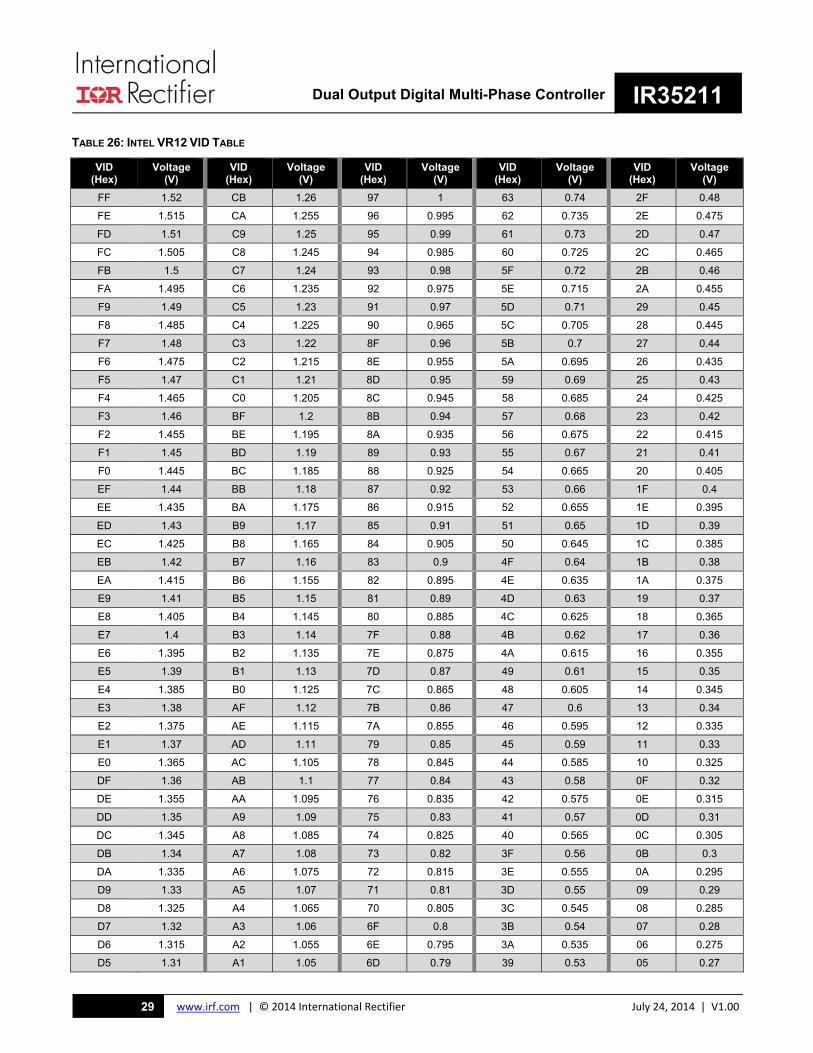
Intel Boot Voltage
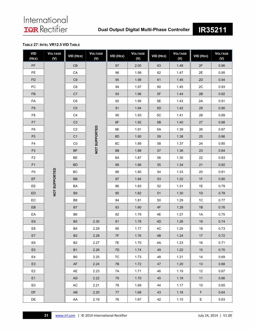
The IR35211 Vboot voltage is fully programmable in MTP to the range shown in Table 18. Table 26 and Table 27 show the Intel/MPoL VID tables for VR12 and VR12.5.
TABLE 18: VBOOT RANGE
Loop Boot Voltage
Loop 1 Per Intel VR12 and VR12.5 VID table
Loop 2 Per Intel VR12 and VR12.5 VID table
Intel SVID Interface
The IR35211 implements a fully compliant VR12 Serial VID (SVID) interface. This is a three-wire interface between a VR12/12.5 compliant processor and a VR that consists of clock, data and alert# signals.
The IR35211 architecture is based upon a digital core and hence lends itself very well to digital communications. As such, the IR35211 implements all the required SVID registers and commands. The IR35211 also implements all the optional commands and registers with only a very few exceptions. The Intel CPU is able to detect and recognize the extra functionality that the IR35211 provides and thus gives the Intel VR12/12.5 CPU unparalleled ability to monitor and optimize its power.
The SVID address of the IR35211 defaults to 0 for loop 1 and 1 for loop 2. The address may be re-programmed in MTP and optionally, the IR35211 may be offset with an external resistor at the ADDR pin (Table 19 and Table 20). Note that a 0.01µF capacitor must be placed across the resistor (Figure 17). An address lock function prevents accidental overwrites of the address.
The pseudo-code below illustrates the MTP address programming:
# unlock the address register to write, then lock Set Address_lock_bit=0 Write new SVID address Set Address_lock_bit=1
TABLE 19: SVID ADDRESS OFFSET OPTIONS
Enable_SVID Addr_Offset MTP bit
SVID Offset
0 disabled
1 enabled
TABLE 20: SVID ADDRESS OFFSET
ADDR Resistor
SVID Address Offset
0.845kΩ 0
1.30kΩ +1
1.78kΩ +2
2.32kΩ +3
2.87kΩ +4
3.48kΩ +5
4.12kΩ +6
4.75kΩ +7
5.49kΩ +8
6.19kΩ +9
6.98kΩ +10
7.87kΩ +11
Figure 17: ADDR Pin Components
Intel VID Offset
The output voltage can be offset according to Table 21. This is especially useful for memory applications where voltages higher than the standard VID table may be required.
TABLE 21: VID OFFSET
Parameter Memory Range Step Size
Output Voltage
R/W -128 to +127
1 VID code
1 Maximum allowed voltage is 1.92V (VR12)

Dual Output Digital Multi-Phase Controller IR35211
www.irf.com | © 2014 International Rectifier July 24, 2014 | V1.0028
Note the Vmax register must be set appropriately to allow the required output voltage offset.
Intel Reporting Offsets
In addition to the mandatory features of the SVID bus, the IR35211 provides optional volatile SVID registers which allow the user to offset the reporting on the SVID interface as detailed in Table 22.
TABLE 22: SVID OFFSET REGISTERS
Parameter Memory Range Step size
Output Current NVM -4A to +3.75A 0.25A
Temperature R/W -32°C to +31°C 1°C
VR12.5 Operation
VR12.5 mode is selectable via either a MTP bit or external pin (INMODE) pulled low. The boot voltage in VR12.5 is also selectable and can be taken from either the boot registers (Table 27) or from 4 fixed VID values (Table 23).
TABLE 23: VR12.5 BOOT VOLTAGES
0V
1.65V
1.7V
1.75V
Memory (MPoL) Mode
In MPoL mode the IR35211 configures Loop 2 VID to 50% of Loop 1. Communication with and control of the IR35211 may occur either through the SVID interface where an Intel SVID Master is present or alternatively through the I2C/SMBus/PMBus interface for non-Intel applications.
The IR35211 follows startup and timing requirements as shown in Figure 18 and Table 24. When the power-on sequence is initiated, and with VBOOT set to > 0V, both rails will ramp to their configured voltages and assert VR_READY_L1 and VR_READY_L2. The slew rates for both loops are set independently per Table 3. If tracking is required during the slew, then care must be taken to ensure that the Loop 2 slew rate is set to ½ of the Loop 1 slew rate. Typical MPoL start-up and shut-down waveforms are shown in Figure 19 and Figure 20.
Figure 18: MPoL Startup
TABLE 24: MPOL START-UP TIMING
Time Description Min Typ Max
TA VR_EN to Loop 1 start 3µs
TB Loop 2 delay Table
25
TC Voltage ramp complete to VR_RDY_L1/L2
1µs
Figure 19: MPoL Tracking Startup
Figure 20: MPoL Tracking Shutdown
In MPoL mode, Loop 2 start-up can be delayed relative to Loop 1 according to Table 25.
TABLE 25: MPOL LOOP 2 START-UP DELAY
Loop 2 Delay
0 – 678.3usec in 2.66usec Steps
Vout 1
Vout 2
Vout 1
Vout 2
Dual Output Digital Multi-Phase Controller IR35211
www.irf.com | © 2014 International Rectifier July 24, 2014 | V1.0029
TABLE 26: INTEL VR12 VID TABLE
VID (Hex)
Voltage (V)
VID (Hex)
Voltage (V)
VID (Hex)
Voltage (V)
VID (Hex)
Voltage (V)
VID (Hex)
Voltage (V)
FF 1.52 CB 1.26 97 1 63 0.74 2F 0.48
FE 1.515 CA 1.255 96 0.995 62 0.735 2E 0.475
FD 1.51 C9 1.25 95 0.99 61 0.73 2D 0.47
FC 1.505 C8 1.245 94 0.985 60 0.725 2C 0.465
FB 1.5 C7 1.24 93 0.98 5F 0.72 2B 0.46
FA 1.495 C6 1.235 92 0.975 5E 0.715 2A 0.455
F9 1.49 C5 1.23 91 0.97 5D 0.71 29 0.45
F8 1.485 C4 1.225 90 0.965 5C 0.705 28 0.445
F7 1.48 C3 1.22 8F 0.96 5B 0.7 27 0.44
F6 1.475 C2 1.215 8E 0.955 5A 0.695 26 0.435
F5 1.47 C1 1.21 8D 0.95 59 0.69 25 0.43
F4 1.465 C0 1.205 8C 0.945 58 0.685 24 0.425
F3 1.46 BF 1.2 8B 0.94 57 0.68 23 0.42
F2 1.455 BE 1.195 8A 0.935 56 0.675 22 0.415
F1 1.45 BD 1.19 89 0.93 55 0.67 21 0.41
F0 1.445 BC 1.185 88 0.925 54 0.665 20 0.405
EF 1.44 BB 1.18 87 0.92 53 0.66 1F 0.4
EE 1.435 BA 1.175 86 0.915 52 0.655 1E 0.395
ED 1.43 B9 1.17 85 0.91 51 0.65 1D 0.39
EC 1.425 B8 1.165 84 0.905 50 0.645 1C 0.385
EB 1.42 B7 1.16 83 0.9 4F 0.64 1B 0.38
EA 1.415 B6 1.155 82 0.895 4E 0.635 1A 0.375
E9 1.41 B5 1.15 81 0.89 4D 0.63 19 0.37
E8 1.405 B4 1.145 80 0.885 4C 0.625 18 0.365
E7 1.4 B3 1.14 7F 0.88 4B 0.62 17 0.36
E6 1.395 B2 1.135 7E 0.875 4A 0.615 16 0.355
E5 1.39 B1 1.13 7D 0.87 49 0.61 15 0.35
E4 1.385 B0 1.125 7C 0.865 48 0.605 14 0.345
E3 1.38 AF 1.12 7B 0.86 47 0.6 13 0.34
E2 1.375 AE 1.115 7A 0.855 46 0.595 12 0.335
E1 1.37 AD 1.11 79 0.85 45 0.59 11 0.33
E0 1.365 AC 1.105 78 0.845 44 0.585 10 0.325
DF 1.36 AB 1.1 77 0.84 43 0.58 0F 0.32
DE 1.355 AA 1.095 76 0.835 42 0.575 0E 0.315
DD 1.35 A9 1.09 75 0.83 41 0.57 0D 0.31
DC 1.345 A8 1.085 74 0.825 40 0.565 0C 0.305
DB 1.34 A7 1.08 73 0.82 3F 0.56 0B 0.3
DA 1.335 A6 1.075 72 0.815 3E 0.555 0A 0.295
D9 1.33 A5 1.07 71 0.81 3D 0.55 09 0.29
D8 1.325 A4 1.065 70 0.805 3C 0.545 08 0.285
D7 1.32 A3 1.06 6F 0.8 3B 0.54 07 0.28
D6 1.315 A2 1.055 6E 0.795 3A 0.535 06 0.275
D5 1.31 A1 1.05 6D 0.79 39 0.53 05 0.27
Dual Output Digital Multi-Phase Controller IR35211
www.irf.com | © 2014 International Rectifier July 24, 2014 | V1.0030
VID (Hex)
Voltage (V)
VID (Hex)
Voltage (V)
VID (Hex)
Voltage (V)
VID (Hex)
Voltage (V)
VID (Hex)
Voltage (V)
D4 1.305 A0 1.045 6C 0.785 38 0.525 04 0.265
D3 1.3 9F 1.04 6B 0.78 37 0.52 03 0.26
D2 1.295 9E 1.035 6A 0.775 36 0.515 02 0.255
D1 1.29 9D 1.03 69 0.77 35 0.51 01 0.25
D0 1.285 9C 1.025 68 0.765 34 0.505 00 0
CF 1.28 9B 1.02 67 0.76 33 0.5
CE 1.275 9A 1.015 66 0.755 32 0.495
CD 1.27 99 1.01 65 0.75 31 0.49
CC 1.265 98 1.005 64 0.745 30 0.485
Dual Output Digital Multi-Phase Controller IR35211
www.irf.com | © 2014 International Rectifier July 24, 2014 | V1.0031
TABLE 27: INTEL VR12.5 VID TABLE
VID
(HEX)
VOLTAGE
(V) VID (HEX)
VOLTAGE
(V) VID (HEX)
VOLTAGE
(V) VID (HEX)
VOLTAGE
(V) VID (HEX)
VOLTAGE
(V)
FF
NO
T S
UP
PO
RT
ED
CB
NO
T S
UP
PO
RT
ED
97 2.00 63 1.48 2F 0.96
FE CA 96 1.99 62 1.47 2E 0.95
FD C9 95 1.98 61 1.46 2D 0.94
FC C8 94 1.97 60 1.45 2C 0.93
FB C7 93 1.96 5F 1.44 2B 0.92
FA C6 92 1.95 5E 1.43 2A 0.91
F9 C5 91 1.94 5D 1.42 29 0.90
F8 C4 90 1.93 5C 1.41 28 0.89
F7 C3 8F 1.92 5B 1.40 27 0.88
F6 C2 8E 1.91 5A 1.39 26 0.87
F5 C1 8D 1.90 59 1.38 25 0.86
F4 C0 8C 1.89 58 1.37 24 0.85
F3 BF 8B 1.88 57 1.36 23 0.84
F2 BE 8A 1.87 56 1.35 22 0.83
F1 BD 89 1.86 55 1.34 21 0.82
F0 BC 88 1.85 54 1.33 20 0.81
EF BB 87 1.84 53 1.32 1F 0.80
EE BA 86 1.83 52 1.31 1E 0.79
ED B9 85 1.82 51 1.30 1D 0.78
EC B8 84 1.81 50 1.29 1C 0.77
EB B7 83 1.80 4F 1.28 1B 0.76
EA B6 82 1.79 4E 1.27 1A 0.75
E9 B5 2.30 81 1.78 4D 1.26 19 0.74
E8 B4 2.29 80 1.77 4C 1.25 18 0.73
E7 B3 2.28 7F 1.76 4B 1.24 17 0.72
E6 B2 2.27 7E 1.75 4A 1.23 16 0.71
E5 B1 2.26 7D 1.74 49 1.22 15 0.70
E4 B0 2.25 7C 1.73 48 1.21 14 0.69
E3 AF 2.24 7B 1.72 47 1.20 13 0.68
E2 AE 2.23 7A 1.71 46 1.19 12 0.67
E1 AD 2.22 79 1.70 45 1.18 11 0.66
E0 AC 2.21 78 1.69 44 1.17 10 0.65
DF AB 2.20 77 1.68 43 1.16 F 0.64
DE AA 2.19 76 1.67 42 1.15 E 0.63
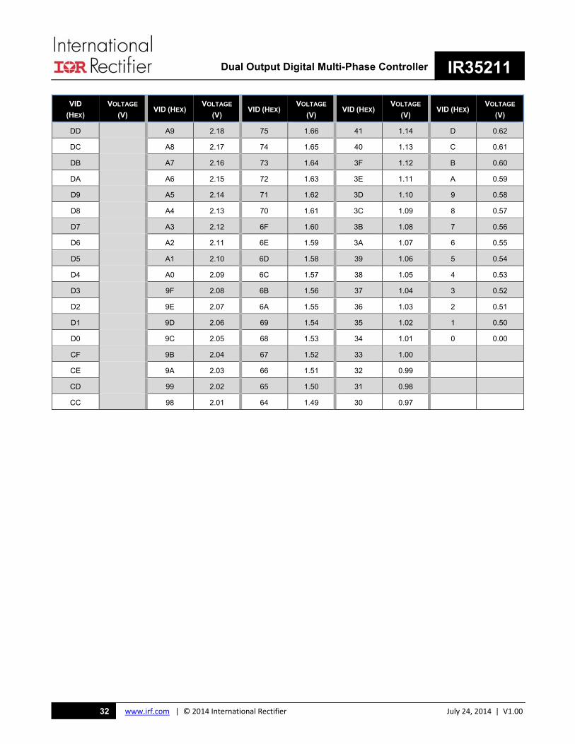
Dual Output Digital Multi-Phase Controller IR35211
www.irf.com | © 2014 International Rectifier July 24, 2014 | V1.0032
VID
(HEX)
VOLTAGE
(V) VID (HEX)
VOLTAGE
(V) VID (HEX)
VOLTAGE
(V) VID (HEX)
VOLTAGE
(V) VID (HEX)
VOLTAGE
(V)
DD A9 2.18 75 1.66 41 1.14 D 0.62
DC A8 2.17 74 1.65 40 1.13 C 0.61
DB A7 2.16 73 1.64 3F 1.12 B 0.60
DA A6 2.15 72 1.63 3E 1.11 A 0.59
D9 A5 2.14 71 1.62 3D 1.10 9 0.58
D8 A4 2.13 70 1.61 3C 1.09 8 0.57
D7 A3 2.12 6F 1.60 3B 1.08 7 0.56
D6 A2 2.11 6E 1.59 3A 1.07 6 0.55
D5 A1 2.10 6D 1.58 39 1.06 5 0.54
D4 A0 2.09 6C 1.57 38 1.05 4 0.53
D3 9F 2.08 6B 1.56 37 1.04 3 0.52
D2 9E 2.07 6A 1.55 36 1.03 2 0.51
D1 9D 2.06 69 1.54 35 1.02 1 0.50
D0 9C 2.05 68 1.53 34 1.01 0 0.00
CF 9B 2.04 67 1.52 33 1.00
CE 9A 2.03 66 1.51 32 0.99
CD 99 2.02 65 1.50 31 0.98
CC 98 2.01 64 1.49 30 0.97

Dual Output Digital Multi-Phase Controller IR35211
www.irf.com | © 2014 International Rectifier July 24, 2014 | V1.0033
PHASING
The number of phases enabled on each loop of the IR35211 is shown in Table 28. The phase of the PWM outputs is automatically adjusted to optimize phase interleaving for minimum output ripple. Phase interleaving results in a ripple frequency that is the product of the switching frequency times the number of phases. A high ripple frequency results in reduced ripple voltage and output filter capacitance requirements.
TABLE 28: LOOP CONFIGURATION
Configuration Loop 1 Loop 2
3+0 3-phases -
2+0 2-phases -
1+0 1-phase -
3+1 3-phases 1-phase
2+1 2-phases 1-phase
1+1 1-phase 1-phase
UNUSED PHASES
Phases are disabled based upon the configuration shown in Table 28. Note that loop phases are disabled in reverse order e.g. in 1+2 mode in the IR35211, phases 3 & 2 are disabled. Disabled PWM outputs should be left floating unless the populated phase detection feature is used.
In addition, the IR35211 detects the number of populated phases at start-up by comparing the voltage on the PWM pin against the phase detection threshold. Unused PWM outputs should be grounded so that their voltage is below the threshold (phase is disabled). The IR35211 will automatically adjust the phase configuration to operate with the populated phases (up to the configuration allowed by the settings in Table 28). In order for populated phases to be detected, the power to the MOSFET driver needs to be powered before Vcc to the controller reaches POR. Unused phases should be disconnected in reverse order to ensure a correct phase relationship. As an example, a configuration must have phase 3 PWM left unconnected to operate in 2+1 mode. If phases 1 or 2 were disconnected instead, the remaining phases would not have a symmetrical relationship leading to poor performance.
Typical PWM pulse phase relationships are shown in Table 29 and Figure 21.
TABLE 29: LOOP 1 PHASE RELATIONSHIP
Loop 1 Phases Phasing
1 -
2 180º
3 120º
Figure 21: 3-phase PWM interleaved operation
SWITCHING FREQUENCY
The phase switching frequency (Fsw) of the IR35211 is set by a user configurable register independently for each loop. The IR35211 provides fine granularity as shown in Figure 22. The IR35211 oscillator is factory trimmed to guarantee absolute accuracy and very low jitter compared to analog controllers.
Figure 22: Switching Frequency Resolution
MOSFET DRIVER AND POWIRSTAGE
SELECTION
Time scale = 1µs/ div
L#1, Φ1
L#1, Φ2
L#1, Φ3
Dual Output Digital Multi-Phase Controller IR35211
www.irf.com | © 2014 International Rectifier July 24, 2014 | V1.0034
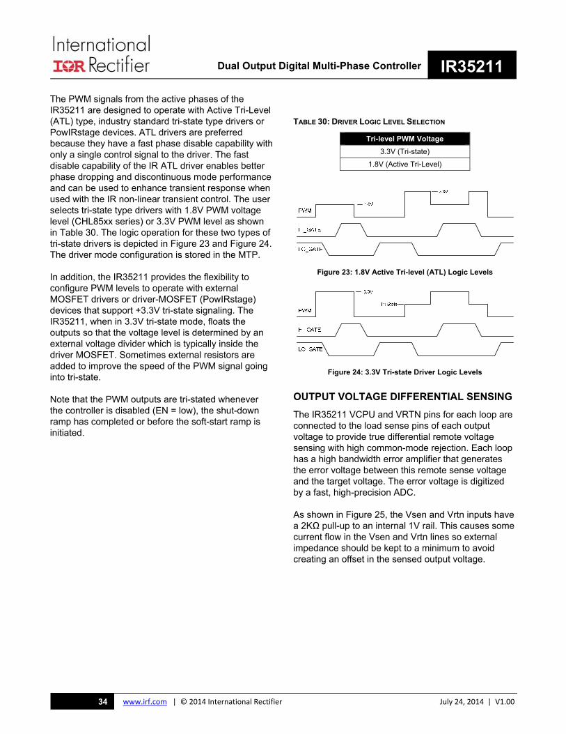
The PWM signals from the active phases of the IR35211 are designed to operate with Active Tri-Level (ATL) type, industry standard tri-state type drivers or PowIRstage devices. ATL drivers are preferred because they have a fast phase disable capability with only a single control signal to the driver. The fast disable capability of the IR ATL driver enables better phase dropping and discontinuous mode performance and can be used to enhance transient response when used with the IR non-linear transient control. The user selects tri-state type drivers with 1.8V PWM voltage level (CHL85xx series) or 3.3V PWM level as shown in Table 30. The logic operation for these two types of tri-state drivers is depicted in Figure 23 and Figure 24. The driver mode configuration is stored in the MTP.
In addition, the IR35211 provides the flexibility to configure PWM levels to operate with external MOSFET drivers or driver-MOSFET (PowIRstage) devices that support +3.3V tri-state signaling. The IR35211, when in 3.3V tri-state mode, floats the outputs so that the voltage level is determined by an external voltage divider which is typically inside the driver MOSFET. Sometimes external resistors are added to improve the speed of the PWM signal going into tri-state.
Note that the PWM outputs are tri-stated whenever the controller is disabled (EN = low), the shut-down ramp has completed or before the soft-start ramp is initiated.
TABLE 30: DRIVER LOGIC LEVEL SELECTION
Tri-level PWM Voltage
3.3V (Tri-state)
1.8V (Active Tri-Level)
Figure 23: 1.8V Active Tri-level (ATL) Logic Levels
Figure 24: 3.3V Tri-state Driver Logic Levels
OUTPUT VOLTAGE DIFFERENTIAL SENSING
The IR35211 VCPU and VRTN pins for each loop are connected to the load sense pins of each output voltage to provide true differential remote voltage sensing with high common-mode rejection. Each loop has a high bandwidth error amplifier that generates the error voltage between this remote sense voltage and the target voltage. The error voltage is digitized by a fast, high-precision ADC.
As shown in Figure 25, the Vsen and Vrtn inputs have a 2KΩ pull-up to an internal 1V rail. This causes some current flow in the Vsen and Vrtn lines so external impedance should be kept to a minimum to avoid creating an offset in the sensed output voltage.
Dual Output Digital Multi-Phase Controller IR35211
www.irf.com | © 2014 International Rectifier July 24, 2014 | V1.0035
Figure 25: Output Voltage sensing impedance
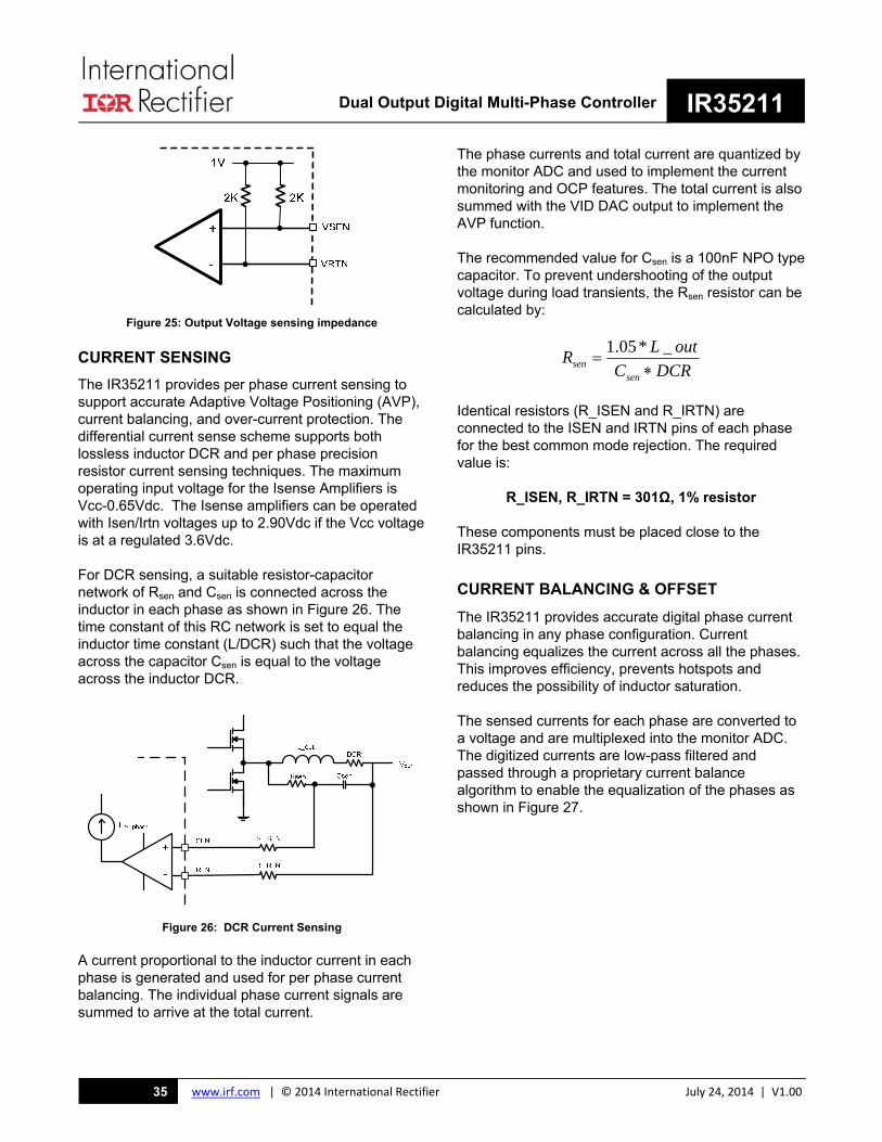
CURRENT SENSING
The IR35211 provides per phase current sensing to support accurate Adaptive Voltage Positioning (AVP), current balancing, and over-current protection. The differential current sense scheme supports both lossless inductor DCR and per phase precision resistor current sensing techniques. The maximum operating input voltage for the Isense Amplifiers is Vcc-0.65Vdc. The Isense amplifiers can be operated with Isen/Irtn voltages up to 2.90Vdc if the Vcc voltage is at a regulated 3.6Vdc.
For DCR sensing, a suitable resistor-capacitor network of Rsen and Csen is connected across the inductor in each phase as shown in Figure 26. The time constant of this RC network is set to equal the inductor time constant (L/DCR) such that the voltage across the capacitor Csen is equal to the voltage across the inductor DCR.
Figure 26: DCR Current Sensing
A current proportional to the inductor current in each phase is generated and used for per phase current balancing. The individual phase current signals are summed to arrive at the total current.
The phase currents and total current are quantized by the monitor ADC and used to implement the current monitoring and OCP features. The total current is also summed with the VID DAC output to implement the AVP function.
The recommended value for Csen is a 100nF NPO type capacitor. To prevent undershooting of the output voltage during load transients, the Rsen resistor can be calculated by:
DCRC
outLR
sensen
_*05.1
Identical resistors (R_ISEN and R_IRTN) are connected to the ISEN and IRTN pins of each phase for the best common mode rejection. The required value is:
R_ISEN, R_IRTN = 301Ω, 1% resistor
These components must be placed close to the IR35211 pins.
CURRENT BALANCING & OFFSET
The IR35211 provides accurate digital phase current balancing in any phase configuration. Current balancing equalizes the current across all the phases. This improves efficiency, prevents hotspots and reduces the possibility of inductor saturation.
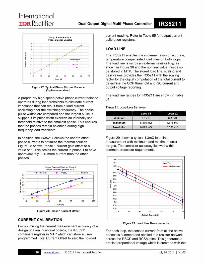
The sensed currents for each phase are converted to a voltage and are multiplexed into the monitor ADC. The digitized currents are low-pass filtered and passed through a proprietary current balance algorithm to enable the equalization of the phases as shown in Figure 27.
Dual Output Digital Multi-Phase Controller IR35211
www.irf.com | © 2014 International Rectifier July 24, 2014 | V1.0036
Figure 27: Typical Phase Current Balance (3-phases enabled)
A proprietary high-speed active phase current balance operates during load transients to eliminate current imbalance that can result from a load current oscillating near the switching frequency. The phase pulse widths are compared and the largest pulse is skipped if its pulse width exceeds an internally set threshold relative to the smallest phase. This ensures that the phases remain balanced during high frequency load transients.
In addition, the IR35211 allows the user to offset phase currents to optimize the thermal solution. Figure 28 shows Phase 1 current gain offset to a value of 6. This scales the current in phase 1 to have approximately 30% more current than the other phases.
Figure 28: Phase 1 Current Offset
CURRENT CALIBRATION
For optimizing the current measurement accuracy of a design or even individual boards, the IR35211 contains a register in MTP which can store a user-programmed Total Current Offset to zero the no-load
current reading. Refer to Table 55 for output current calibration registers.
LOAD LINE
The IR35211 enables the implementation of accurate, temperature compensated load lines on both loops. The load line is set by an external resistor RCS, as shown in Figure 30 and the nominal value must also be stored in MTP. The stored load line, scaling and gain values provides the IR35211 with the scaling factor for the digital computation of the total current to determine the OCP threshold and I2C current and output voltage reporting.
The load line ranges for IR35211 are shown in Table 31.
TABLE 31: LOAD LINE SETTINGS
Loop #1 Loop #2
Minimum 0.0 mΩ 0.0 mΩ
Maximum 6.375 mΩ 12.75 mΩ
Resolution 0.025 mΩ 0.050 mΩ
Figure 29 shows a typical 1.3mΩ load line measurement with minimum and maximum error ranges. The controller accuracy lies well within common processor requirements.
Figure 29: Load Line Measurements
For each loop, the sensed current from all the active phases is summed and applied to a resistor network across the RSCP and RCSM pins. This generates a precise proportional voltage which is summed with the
0.76
0.78
0.8
0.82
0.84
0.86
0.88
0.9
0.92
0.94
0.96
0.98
1
1.02
1.04
1.06
0 25 50 75 100 125 150
Output Current (A)
Vo
ut
(V)
Vout
CPU Min/Max

Dual Output Digital Multi-Phase Controller IR35211
www.irf.com | © 2014 International Rectifier July 24, 2014 | V1.0037
sensed output voltage and VID DAC reference to form the error voltage. Also part of the network shown in Figure 30 is thermistor, RTh. For proper load line temperature compensation, the thermistor is placed near the phase one inductor to accurately sense the inductor temperature.
Figure 30: Load Line & Thermal Compensation
The resistor RCS is calculated using the following procedure:
First the designer calculates the RCSeffective or the total effective parallel resistance across the RSCP and RCSM pins. It is defined by:
DCR
RISENRR LL
effectiveCS _8
Where RLL is the desired load line, typically 1.0mΩ, DCR is DC resistance of the phase inductor, and R_ISEN is the series resistor across the inductor sense circuit. The required value for R_ISEN is a 301Ω, 1% tolerance. Then the designer chooses a suitable NTC thermistor. Thermistor Rth is typically selected to have the lowest thermal coefficient and tightest tolerance in a standard available package. A typical value for the NTC will be 10kΩ, 1% tolerance. Recommended thermistors are shown in Table 32.
TABLE 32: 10K 1% NTC THERMISTORS
Murata NCP18XH103F03RB
Panasonic ERTJ1VG103FA
TDK NTCG163JF103F
Then the designer calculates RCS the using the following equation:
ThserieseffectiveCS
CS
R
1
R2R
11
R
Rseries is selected to achieve minimum load line error over temperature. The IR DPDC provides a graphical tool that allows the user to easily calculate the resistor values for minimum error.
The capacitor CCS is defined by the following equation:
AVPCS fveRCSeffecti
C
2
1
where, fAVP is the user selectable current sense AVP bandwidth. The best bandwidth is typically in the range of 200kHz to 300kHz.
Setting 0mΩ Load Line
The load line is turned off by setting a digital bit in the IR35211 register map. This is a separate bit from the load line settings for each loop.
Even though the load line is disabled digitally, the resistors and load line and scaling registers should be set such that the load line is at least 3 times the value of low ohmic DCR inductors (<0.5mΩ) or 1 times the DCR value for high ohmic inductors (>0.5mΩ), e.g. if the inductor(s) DCR is 0.3mΩ, a nominal 0.9 mΩ load line should be set. For accurate current measurement and OCP threshold with the load line disabled, the output current gain and scaling registers must be set to the same value as the load line set with the external resistor network. With load line disabled, the thermistor and Css capacitor must still be installed to insure accuracy of the current measurement.
DIGITAL FEEDBACK LOOP & PWM
The IR35211 uses a digital feedback loop to minimize the requirement for output decoupling and maintain a tightly regulated output voltage. The error between the target and the output voltage is digitized. This error voltage is then passed through a low pass filter to smooth ripple and then passed through a PID (Proportional Integral Derivative) compensator followed by an additional single pole filter. The loop compensation parameters Kp (proportional coefficient), KI (integral coefficient), and KD (derivative coefficient) and low-pass filter pole locations are user configurable to optimize the VR design for the chosen external components.

Dual Output Digital Multi-Phase Controller IR35211
www.irf.com | © 2014 International Rectifier July 24, 2014 | V1.0038
The IR35211 significantly reduces design time because the loop coefficients need to be calculated only once. Simply enable any number of phases and design the compensation coefficients. The IR35211 will intelligently scale the coefficients and low-pass filters automatically as phases dynamically add and drop to maintain optimum stability (Figure 31).
Figure 31: Stability with Phase Add/Drop
Each of the proportional, integral and derivative terms is a 6-bit value stored in MTP that is decoded by the IC’s digital code. This allows the designer to set the converter bandwidth and phase margin to the desired values.
The compensator transfer function is defined as:
211
1
1
1)(
ps
ps
sKds
KiKp
where ωp1 and ωp2 are configurable poles typically positioned to filter noise and ripple and roll off the high-frequency gain that the KD term creates.
The outputs of the compensator and the phase current balance block are fed into a digital PWM pulse generator to generate the PWM pulses for the active phases. The digital PWM generator has a native time resolution of 625ps which is combined with digital dithering to provide an effective PWM resolution of 156.25ps. This ensures that there is no limit cycling when operating at the highest switching frequency.
ADAPTIVE TRANSIENT ALGORITHM (ATA)
The IR35211 Adaptive Transient Algorithm (ATA) is a high speed non-linear control technique that allows compliance with CPU voltage transient load regulation requirements with minimum output bulk capacitance for reduced system cost.
A high-speed digitizer measures both the magnitude and slope of the error signal to predict the load current transient. This prediction is used to control the pulse widths and the phase relationships of the PWM pulses. The ATA bypasses the PID control momentarily during load transients to achieve very wideband closed loop control and smoothly transitions back to PID control during steady state load conditions. Figure 32 illustrates the transient performance improvement provided by the ATA showing the clear reduction in undershoot and overshoot. Figure 33 is a close up of a loadstep illustrating the fast reaction time of ATA and how the algorithm changes the pulse phase relationships. ATA can be disabled if desired.
Figure 32: ATA Enable/Disable Comparison
Figure 33: ATA close up
ATA Disabled
ATA Enabled
Vout
Iout

Dual Output Digital Multi-Phase Controller IR35211
www.irf.com | © 2014 International Rectifier July 24, 2014 | V1.0039
During a load transient overshoot, the ATA can also be programmed to turn off the low-side MOSFETS instead of holding them on. This forces the load current to flow through the larger forward voltage of the FET body diode and helps to reduce the overshoot created during a load release (Figure 34).
Figure 34: Diode Emulation during a load release
HIGH-SPEED PHASE BALANCE
The IR35211 provides phase balance during high frequency load oscillations. The balance is provided through phase skipping. Whenever a set error voltage threshold, load oscillation frequency threshold, and a pulse width delta threshold is exceeded for a particular phase, that phase is skipped resulting in a lowering of current in the skipped phase and a corresponding increase in current in the other phases. All three thresholds in Table 33 are user programmable to provide flexibility in high-speed phase balance for a wide variety of systems.
TABLE 33: HIGH-SPEED THRESHOLDS
Register Function
Hspb_delta Pulse width delta threshold. Difference between the average of a particular phase pulse width and the average of all other phase pulse widths. Phase is skipped when its pulse width delta exceeds the threshold.
Disable HSPB, 40nsec – 600nsec, 40nsec resolution.
Hspb_hth Error Voltage threshold.
Activates HSPB when the threshold is exceeded.
0mV – 60mV, 4mV resolution
Hspb_fth Load Oscillation Frequency Threshold.
Activates HSPB when the load oscillation frequency is above threshold.
0kHz – 703.5kHz, 46.9kHz resolution.
DYNAMIC VID SLEW RATE
The IR35211 provides the VR designer with 4 slew rates in AMD SVI2 mode up to 25mV/us (Fast rate only) and up to 12 slew rates in Intel mode by selecting a slew rate setting as shown in Table 34. These slew rates can be further reduced by 10x by a register bit setting.
TABLE 34: SLEW RATES
mV/µs
FAST rate ½ Multiplier ¼ Multiplier
10 5.0 2.50
15 7.5 3.75
20 10 5.00
25 12.5 6.25
DYNAMIC VID COMPENSATION
The IR35211 can compensate for the error produced by the current feedback in a system with AVP (Active Voltage Positioning) when the output voltage is ramping to a higher voltage. MTP parameters are provided that set an output capacitance term and an AVP bandwidth term such that the user can model the effects that the inrush current into the output bulk capacitors has on the error voltage and thus the output voltage when the voltage is ramping to a higher voltage. Once properly modeled the output voltage will more closely follow the DAC during a positive dynamic VID and provide better dynamic VID alert timing required by Intel® and AMD® processors. Figure 35 shows the effects that Dynamic VID Compensation has on the output voltage and the alert timing.
Figure 35: Dynamic VID Compensation
Diode Emulation: Disabled Enabled
No DVID Compensation
DVID Compensation set to model ~7500uF of output capacitance

Dual Output Digital Multi-Phase Controller IR35211
www.irf.com | © 2014 International Rectifier July 24, 2014 | V1.0040
EFFICIENCY SHAPING
In addition to CPU-specified Power States, the IR35211 features Efficiency Shaping Technology that enables VR designers to cost-effectively maximize system efficiency. Efficiency Shaping Technology consists of Dynamic Phase Control to achieve the best VR efficiency at a given cost point.
POWER-SAVING STATES
The IR35211 uses Power States to set the operating mode. These are summarized in Table 35.
TABLE 35: POWER STATES
Power State
Mode Recommended
Current
PS0 Full Power Maximum
PS1 Light Load 1Φ <20A
PS2 1Φ Active Discontinuous
(Diode Emulation) <5A
The Power States may be commanded through I2C/PMBus, the SVI interface or the IR35211 can autonomously step through the Power States based upon the regulator conditions as summarized in Table 36.
TABLE 36: POWER STATE ENTRY/EXIT
Command Mode Auto Mode
PS1 Entry
a) Command n/a if Phase Shed enabled
PS1 Exit
a) Command to PS0
b) DVID to PS0
c) Current limit to PS0
n/a if Phase Shed enabled
PS2 Entry
a) Command Current level in 1Φ
PS2 Exit
a) Command to PS1
b) DVID to PS0
c) Current limit to PS0
Fsw > Fsw_desired
to PS0, DVID to PS0,
Current limit to PS0
DYNAMIC PHASE CONTROL (DPC)
IN PS0, PS1
IR35211 optionally supports the ability to auto-nomously adjust the number of phases with load current, thus optimizing efficiency over a wide range of loads. The output current level at which a phase is added can be programmed individually for each phase for optimum results (Table 37)
TABLE 37: DPC THRESHOLDS
Register (2A steps) Function
Phase1_thresh 2Φ when I > Phase1_thresh
Phase2_delta 3Φ when I > Phase1_thresh + Phase2_delta
As shown in Figure 37, (loop one, 3-phase example shown), the designer can configure the VR to dynamically add or shed phases as the load current varies.
Figure 37: Dynamic Phase Control Regions
The IR35211 Dynamic Phase Control reduces the number of phases (Figure 38) based upon monitoring both filtered total current and error voltage over the DPC filter window. Monitoring the error voltage insures that the VR will not drop phases during large load oscillations.
Per-phase Programmable
Threshold for Auto Phase Shed
Load Current
E ff
i ci e
n cy
3 Ø2Ø1Ø
Programmable Threshold for
Auto DCM
DC
M
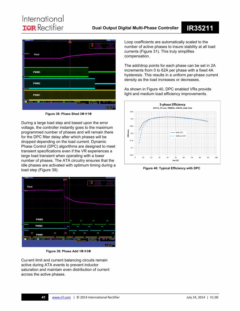
Dual Output Digital Multi-Phase Controller IR35211
www.irf.com | © 2014 International Rectifier July 24, 2014 | V1.0041
Figure 38: Phase Shed 3Φ1Φ
During a large load step and based upon the error voltage, the controller instantly goes to the maximum programmed number of phases and will remain there for the DPC filter delay after which phases will be dropped depending on the load current. Dynamic Phase Control (DPC) algorithms are designed to meet transient specifications even if the VR experiences a large load transient when operating with a lower number of phases. The ATA circuitry ensures that the idle phases are activated with optimum timing during a load step (Figure 39).
Figure 39: Phase Add 1Φ3Φ
Current limit and current balancing circuits remain active during ATA events to prevent inductor saturation and maintain even distribution of current across the active phases.
Loop coefficients are automatically scaled to the number of active phases to insure stability at all load currents (Figure 31). This truly simplifies compensation.
The add/drop points for each phase can be set in 2A increments from 0 to 62A per phase with a fixed 4A hysteresis. This results in a uniform per-phase current density as the load increases or decreases.
As shown in Figure 40, DPC enabled VRs provide light and medium load efficiency improvements.
Figure 40: Typical Efficiency with DPC
PWM1
PWM2
PWM3
Vout
Vout
Vdd
Idd
PWM1
PWM2
PWM3
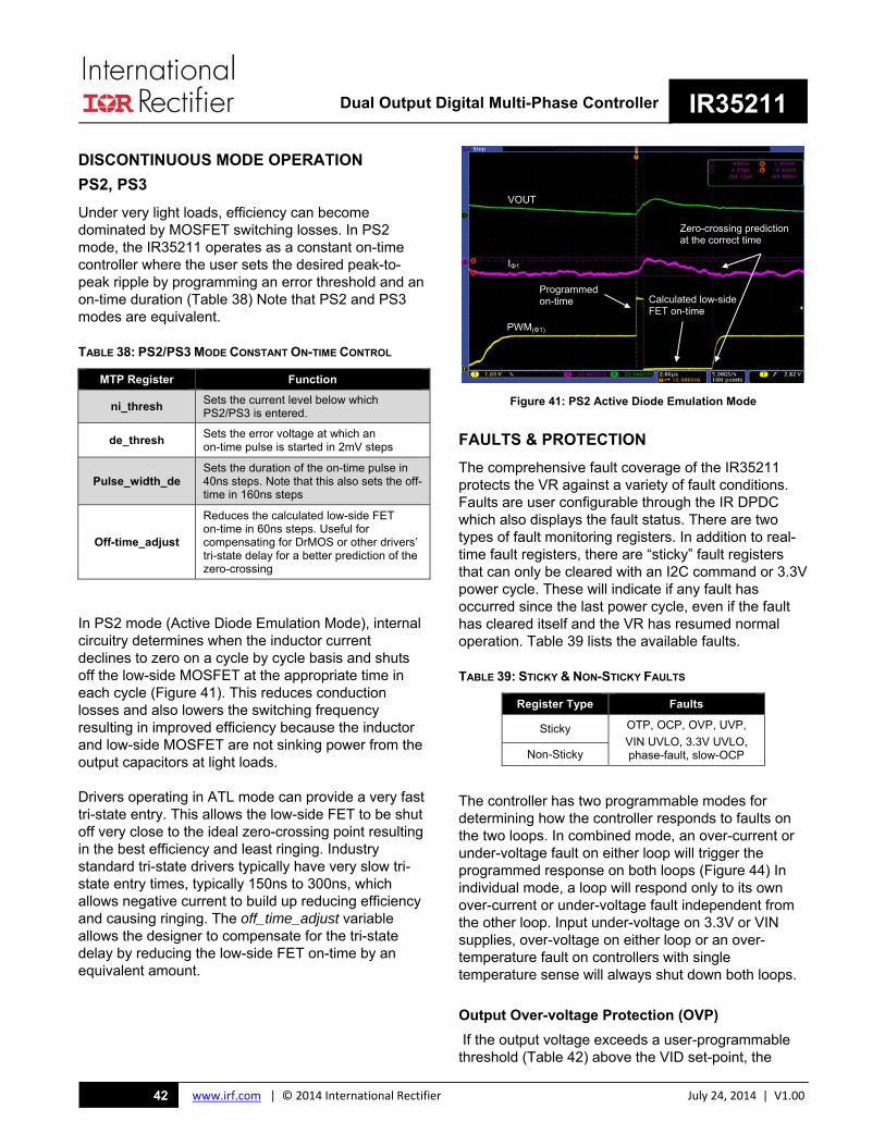
Dual Output Digital Multi-Phase Controller IR35211
www.irf.com | © 2014 International Rectifier July 24, 2014 | V1.0042
DISCONTINUOUS MODE OPERATION
PS2, PS3
Under very light loads, efficiency can become dominated by MOSFET switching losses. In PS2 mode, the IR35211 operates as a constant on-time controller where the user sets the desired peak-to-peak ripple by programming an error threshold and an on-time duration (Table 38) Note that PS2 and PS3 modes are equivalent.
TABLE 38: PS2/PS3 MODE CONSTANT ON-TIME CONTROL
MTP Register Function
ni_thresh Sets the current level below which PS2/PS3 is entered.
de_thresh Sets the error voltage at which an on-time pulse is started in 2mV steps
Pulse_width_de Sets the duration of the on-time pulse in 40ns steps. Note that this also sets the off-time in 160ns steps
Off-time_adjust
Reduces the calculated low-side FET on-time in 60ns steps. Useful for compensating for DrMOS or other drivers’ tri-state delay for a better prediction of the zero-crossing
In PS2 mode (Active Diode Emulation Mode), internal circuitry determines when the inductor current declines to zero on a cycle by cycle basis and shuts off the low-side MOSFET at the appropriate time in each cycle (Figure 41). This reduces conduction losses and also lowers the switching frequency resulting in improved efficiency because the inductor and low-side MOSFET are not sinking power from the output capacitors at light loads.
Drivers operating in ATL mode can provide a very fast tri-state entry. This allows the low-side FET to be shut off very close to the ideal zero-crossing point resulting in the best efficiency and least ringing. Industry standard tri-state drivers typically have very slow tri-state entry times, typically 150ns to 300ns, which allows negative current to build up reducing efficiency and causing ringing. The off_time_adjust variable allows the designer to compensate for the tri-state delay by reducing the low-side FET on-time by an equivalent amount.
Figure 41: PS2 Active Diode Emulation Mode
FAULTS & PROTECTION
The comprehensive fault coverage of the IR35211 protects the VR against a variety of fault conditions. Faults are user configurable through the IR DPDC which also displays the fault status. There are two types of fault monitoring registers. In addition to real-time fault registers, there are “sticky” fault registers that can only be cleared with an I2C command or 3.3V power cycle. These will indicate if any fault has occurred since the last power cycle, even if the fault has cleared itself and the VR has resumed normal operation. Table 39 lists the available faults.
TABLE 39: STICKY & NON-STICKY FAULTS
Register Type Faults
Sticky OTP, OCP, OVP, UVP,
VIN UVLO, 3.3V UVLO, phase-fault, slow-OCP Non-Sticky
The controller has two programmable modes for determining how the controller responds to faults on the two loops. In combined mode, an over-current or under-voltage fault on either loop will trigger the programmed response on both loops (Figure 44) In individual mode, a loop will respond only to its own over-current or under-voltage fault independent from the other loop. Input under-voltage on 3.3V or VIN supplies, over-voltage on either loop or an over-temperature fault on controllers with single temperature sense will always shut down both loops.
Output Over-voltage Protection (OVP)
If the output voltage exceeds a user-programmable threshold (Table 42) above the VID set-point, the
VOUT
IΦ1
PWM(Φ1)
Programmed on-time Calculated low-side
FET on-time
Zero-crossing prediction at the correct time
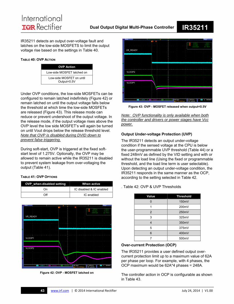
Dual Output Digital Multi-Phase Controller IR35211
www.irf.com | © 2014 International Rectifier July 24, 2014 | V1.0043
IR35211 detects an output over-voltage fault and latches on the low-side MOSFETS to limit the output voltage rise based on the settings in Table 40.
TABLE 40: OVP ACTION
OVP Action
Low-side MOSFET latched on
Low-side MOSFET on until Output<0.5V
Under OVP conditions, the low-side MOSFETs can be configured to remain latched indefinitely (Figure 42) or remain latched on until the output voltage falls below the threshold at which time the low-side MOSFETs are released (Figure 43). This release mode can reduce or prevent undershoot of the output voltage. In the release mode, if the output voltage rises above the OVP level the low side MOSFET’s will again be turned on until Vout drops below the release threshold level. Note that OVP is disabled during DVID down to prevent false triggering.
During soft-start, OVP is triggered at the fixed soft-start level of 1.275V. Optionally, the OVP may be allowed to remain active while the IR35211 is disabled to prevent system leakage from over-voltaging the output (Table 41).
TABLE 41: OVP OPTIONS
OVP_when-disabled setting When active
On IC disabled & IC enabled
Off IC enabled
Figure 42: OVP - MOSFET latched on
Figure 43: OVP - MOSFET released when output<0.5V
Note: OVP functionality is only available when both the controller and drivers or power stages have Vcc power.
Output Under-voltage Protection (UVP)
The IR35211 detects an output under-voltage condition if the sensed voltage at the CPU is below the user-programmable UVP threshold (Table 44) or a fixed 248mV as defined by the VID setting and with or without the load line (Using the fixed or programmable threshold, and the load line term is user selectable). Upon detecting an output under-voltage condition, the IR35211 responds in the same manner as the OCP, according to the setting selected in Table 42.
. Table 42: OVP & UVP Thresholds
Value Threshold
0 150mV
1 200mV
2 250mV
3 325mV
4 350mV
5 375mV
6 400mV
7 500mV
Over-current Protection (OCP)
The IR35211 provides a user defined output over-current protection limit up to a maximum value of 62A per phase per loop. For example, with 4 phases, the OCP maximum would be 62A*4 phases = 248A.
The controller action in OCP is configurable as shown in Table 43.
VLOOP2
VLOOP1
VR_READY
VR_READY
VLOOP2
VLOOP1
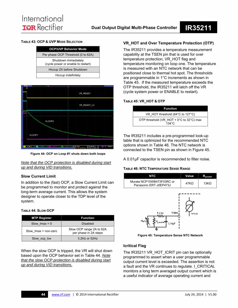
Dual Output Digital Multi-Phase Controller IR35211
www.irf.com | © 2014 International Rectifier July 24, 2014 | V1.0044
TABLE 43: OCP & UVP MODE SELECTION
OCP/UVP Behavior Mode
Per phase OCP Threshold (0 to 62A)
Shutdown immediately (cycle power or enable to restart)
Hiccup 2X before Shutdown
Hiccup indefinitely
Figure 44: OCP on Loop #1 shuts down both loops
Note that the OCP protection is disabled during start up and during VID transitions.
Slow Current Limit
In addition to the (fast) OCP, a Slow Current Limit can be programmed to monitor and protect against the long-term average current. This allows the system designer to operate closer to the TDP level of the system.
TABLE 44: SLOW OCP
MTP Register Function
Slow_Imax = 0 Disabled
Slow_Imax = non-zero Slow OCP range 2A to 62A
per phase in 2A steps
Slow_ocp_bw 3.2Hz or 52Hz
When the slow OCP is tripped, the VR will shut down based upon the OCP behavior set in Table 44. Note that the slow OCP protection is disabled during start up and during VID transitions.
VR_HOT and Over Temperature Protection (OTP)
The IR35211 provides a temperature measurement capability at the TSEN pin that is used for over temperature protection, VR_HOT flag and temperature monitoring on loop one. The temperature is measured with an NTC network that can be positioned close to thermal hot spot. The thresholds are programmable in 1°C increments as shown in Table 45. If the measured temperature exceeds the OTP threshold, the IR35211 will latch off the VR (cycle system power or ENABLE to restart).
TABLE 45: VR_HOT & OTP
Function
VR_HOT threshold (64°C to 127°C)
OTP threshold (VR_HOT + 0°C to 32°C) max 134°C
The IR35211 includes a pre-programmed look-up table that is optimized for the recommended NTC options shown in Table 46. The NTC network is connected to the TSEN pin as shown in Figure 45.
A 0.01µF capacitor is recommended to filter noise.
TABLE 46: NTC TEMPERATURE SENSE RANGE
NTC Value Rparallel
Murata NCP15WB473F03RC or Panasonic ERT-J0EP473J
47KΩ 13KΩ
Figure 45: Temperature Sense NTC Network
Icritical Flag
The IR35211 VR_HOT_ICRIT pin can be optionally programmed to assert when a user programmable output current level is exceeded. The assertion is not a fault and the VR continues to regulate. I_CRITICAL monitors a long term averaged output current which is a useful indicator of average operating current and
VR_READY
VR_READY_L2
VLOOP2
VLOOP1
Dual Output Digital Multi-Phase Controller IR35211
www.irf.com | © 2014 International Rectifier July 24, 2014 | V1.0045
thermal operation. The user can select between two I_CRITICAL filters bandwidths (Table 47).
TABLE 47: OUTPUT OVER-CURRENT OPTIONS
Slow
Very Slow
Refer to electrical table for Iout filter values
I_CRITICAL has a 5% hysteresis level and the VR_HOT_ICRIT pin will de-assert when the average output current level drops below 95% of the programmed current level threshold.
Pin Critical Flag
Additionally the IR35211 can be programmed to assert VR_HOT_ICRIT pin when a user programmable input power level is exceeded. The assertion is not a fault and the VR continues to regulate. PIN_CRITICAL monitors a long term average input power as calculated from the output current. The equation below shows the calculation performed by the IC to determine the average input power.
Where D is the duty cycle and η is the efficiency (fixed at 85%).
The PIN_CRITICAL power level can be programmed in MTP in 4W steps up to 252W, and if set (must be >8W), is wired OR’d into the VR_HOT_ICRIT pin. PIN_CRITICAL has a fixed 8W hysteresis level and the VR_HOT_ICRIT pin will de-assert when the power level drops 8W below the programmed input power level threshold.
VR_HOT_ICRIT Pin Functionality Options
The functionality of the VR_HOT_ICRIT pin can be set to assert when levels of Temp_max, Icc_max, and/or OCP levels are exceeded. Table 48 shows the multiple configurations of the VR_HOT_ICRIT pin.
TABLE 48: VR_HOT_ICRIT PIN OPTIONS
Temp_max Only
Temp_max or Icc_max
Temp_max or OCP
Icc_max Only
Input Over-voltage Protection
As well as under-voltage, the main converter input power supply can be protected for over-voltage. If enabled (Table 49) the VINSEN pin is compared to a fixed threshold and the IC will shut down if the threshold is exceeded. Thresholds are 14.5V (14:1 divider) and 23.5V (22:1 divider).
TABLE 49: INPUT OVER-VOLTAGE OPTIONS
disabled
enabled
Phase Faults
The IR35211 can detected and declared a phase fault when the current in one or more phases is too high or low. It detects the fault when the duty cycle of a particular phase is 0.05 higher or lower than the average duty cycle of all the phases. This feature helps detect severe imbalances in the phase currents, an unpowered or damaged MOSFET driver, or a phase that is disconnected from Vin. The phase fault feature can be enabled or disabled through a MTP bit. When a phase fault occurs the contoller shuts down the loop where the fault occurred and sets register bits to display which phase had the fault and whether it faulted high or low. The phase fault registers are cleared via a register bit and the VR will restart once ENABLE or Vcc is cycled.
TABLE 50: PHASE FAULT REGISTERS
Register Function
Phase_I_fault_enable Enables phase fault detection
Clear_phase_fault Clears all phase faults for each loop.
Phase_fault
Indicates which phase has a phase current fault. 0 – phase1, 1 – phase2, 2 – phase3, 3 – phase4, 4 – phase5, 5 – phase6, 6 – phase7, 7 – phase8.
max_current Indicates one or more phase currents are too high.
min_current Indicates one or more phase currents are too low.
PINIout D
VIN

Dual Output Digital Multi-Phase Controller IR35211
www.irf.com | © 2014 International Rectifier July 24, 2014 | V1.0046
I2C/PMBUS COMMUNICATION
The IR35211 simultaneously supports I2C and PMBus through the use of exclusive addressing. The I2C and PMBus address for the IR35211 is programmed by MTP bits in Table 51. This means that a motherboard PMBus master may communicate with typically up to 8 dual loops, or if used as single loop controllers, as many as 16 IR35211-based VRs. Optionally, a resistor offset can be enabled as shown in Table 52 (note that a 0.01µF capacitor is required across the resistor per Figure 46. As an example, setting a base I2C address of 28h with a resistor offset of +15 sets the I2C address to 37h. Similarly setting a base PMBus address of 40h with a resistor offset of +15 sets the PMBus address to 77h. Note that a single I2C address operates both loops whereas Table 51 sets the PMBus address of Loop 1, while Loop 2 is offset higher by the Chip_Addr_Offset register which is defaulted to 1.
OffsetAddrChipPMaddressPMaddress LoopLoop __12
The IR35211 can also set the I2C address independently from the PMBus address. By using a 7-bit address the user can configure the device to any one of 127 different I2C addresses. Note that I2C address 00h is not allowed. This is an I2C broadcast address. Setting the I2C address to 00h forces the I2C address to follow the PMBus address per Table 51.
Once the address of the IR35211 is set, it is locked to protect it from being overridden.
For default programmed devices, the I2C/PMBus address can be temporarily forced to address 0Ah for I2C and 0Dh for PMBus by setting EN=VR_HOT=low.
TABLE 51: PMBUS/I2C ADDRESSING
Register Setting PM_Addr<3:0>
Calculated 8 Bit
address code
PMBus 7-bit
Address
I2C 7-bit
Address when tied to PMBus
1
1111 1110 1110 77 hex 37 hex
1110 1110 1100 76 hex 36 hex
1101 1110 1010 75 hex 35 hex
1100 1110 1000 74 hex 34 hex
1011 1110 0110 73 hex 33 hex
1010 1110 0100 72 hex 32 hex
1001 1110 0010 71 hex 31 hex
1000 1110 0000 70 hex 30 hex
0111 1000 1110 47 hex 2F hex
0110 1000 1100 46 hex 2E hex
0101 1000 1010 45 hex 2D hex
0100 1000 1000 44 hex 2C hex
0011 1000 0110 43 hex 2B hex
0010 1000 0100 42 hex 2A hex
0001 1000 0010 41 hex 29 hex
0000 1000 0000 40 hex 28 hex
EN=VR_HOT=low 0001 1010 0D hex 0A hex
Note 1: This I2C Address only takes effect if Register 0x12[6:0]=0000000.
TABLE 52: I2C OFFSET OPTIONS
Enable_I2C Addr_Offset MTP bit
I2C Address Offset
0 disabled
1 enabled

Dual Output Digital Multi-Phase Controller IR35211
www.irf.com | © 2014 International Rectifier July 24, 2014 | V1.0047
TABLE 53: ADDR RESISTOR OFFSET
ADDR Resistor I2C Address
Offset
0.845kΩ +0
1.30kΩ +1
1.78kΩ +2
2.32kΩ +3
2.87kΩ +4
3.48kΩ +5
4.12kΩ +6
4.75kΩ +7
5.49kΩ +8
6.19kΩ +9
6.98kΩ +10
7.87kΩ +11
8.87kΩ +12
10.00kΩ +13
11.00kΩ +14
12.10kΩ +15
*Note: Extends the range of PMBus addresses.
Figure 46: ADDR pin components
REAL-TIME I2C MONITORING FUNCTIONS
IR35211 provides real-time accurate measurement of input voltage, input current, output voltage, output current and temperature over the I2C interface. Output voltage is calculated based upon the VID setting and load line and the result is reported through the I2C.
Accuracy Optimization Registers
The IR35211 provides excellent factory-trimmed chip accuracy. In addition, the designer has calibration capability that can be used to optimize accuracy for a given design with minimum component changes. Once a design has been optimized the IR35211 will provide excellent repeatability from board to board. The IR35211 also provides the capability for individual board calibration and programming in production for the best accuracy.
Table 54 shows the MTP registers used to fine tune the accuracy of the reported measurements.
Figure 47 to Figure 49 show the typical accuracy of the output current, input voltage and output voltage measurements using the IR35211.
TABLE 54: ACCURACY OPTIMIZATION REGISTERS
NVM Register Function
IIN Fixed Offset Offsets the input current in 1/32A steps e.g. driver Icc which can be 5-8mA per driver
IIN Per Phase Offset
Offsets the input current dependent upon the number of active phases in 1/128A steps e.g. the drive current for the MOSFET‟s. This current increases every time a new phase is added
IOUT Current Offset
Offsets the output current from -8A to +7.5A in 0.5A steps (loop 1) and -4A to +3.75A 0.25A steps (loop 2)
Vout Offset Offsets the output voltage +40mV to -35mV in 5mV steps (Intel mode) or +50mV to
-43.75mV in 6.25mV steps (AMD)
Temperature Offset
Offsets the temperature in 1°C steps e.g. to compensate for offset between the hottest component and the NTC sensing location.
Figure 47: I2C IOUT Error using 10% DCR Inductors
Figure 48: I2C Input Voltage Measurements
-20%
-15%
-10%
-5%
0%
5%
10%
15%
20%
0 10 20 30 40 50 60 70 80 90 100
Err
or
E-Load (A)
Iout Error
CPU spec with 7% inductors
-1.0%
-0.5%
0.0%
0.5%
1.0%
11.7
11.8
11.9
12
12.1
12.2
12.3
0 20 40 60 80 100
Err
or
Vin
(V)
E-Load (A)
Vin (DMM)
Vin (I2C)
Vin error (2nd axis)
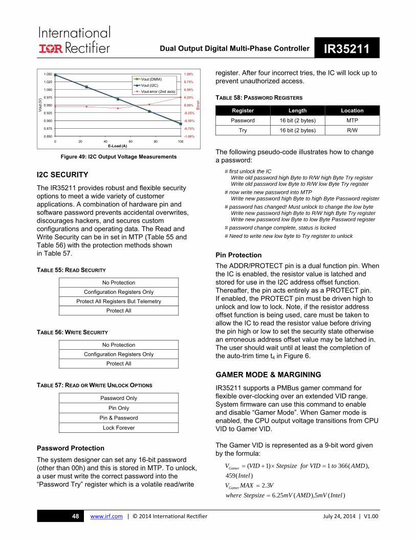
Dual Output Digital Multi-Phase Controller IR35211
www.irf.com | © 2014 International Rectifier July 24, 2014 | V1.0048
Figure 49: I2C Output Voltage Measurements
I2C SECURITY
The IR35211 provides robust and flexible security options to meet a wide variety of customer applications. A combination of hardware pin and software password prevents accidental overwrites, discourages hackers, and secures custom configurations and operating data. The Read and Write Security can be in set in MTP (Table 55 and Table 56) with the protection methods shown in Table 57.
TABLE 55: READ SECURITY
No Protection
Configuration Registers Only
Protect All Registers But Telemetry
Protect All
TABLE 56: WRITE SECURITY
No Protection
Configuration Registers Only
Protect All
TABLE 57: READ OR WRITE UNLOCK OPTIONS
Password Only
Pin Only
Pin & Password
Lock Forever
Password Protection
The system designer can set any 16-bit password (other than 00h) and this is stored in MTP. To unlock, a user must write the correct password into the “Password Try” register which is a volatile read/write
register. After four incorrect tries, the IC will lock up to prevent unauthorized access.
TABLE 58: PASSWORD REGISTERS
Register Length Location
Password 16 bit (2 bytes) MTP
Try 16 bit (2 bytes) R/W
The following pseudo-code illustrates how to change a password:
# first unlock the IC Write old password high Byte to R/W high Byte Try register Write old password low Byte to R/W low Byte Try register
# now write new password into MTP Write new password high Byte to high Byte Password register
# password has changed! Must unlock to change the low byte Write new password high Byte to R/W high Byte Try register Write new password low Byte to low Byte Password register
# password change complete, status is locked
# Need to write new low byte to Try register to unlock
Pin Protection
The ADDR/PROTECT pin is a dual function pin. When the IC is enabled, the resistor value is latched and stored for use in the I2C address offset function. Thereafter, the pin acts entirely as a PROTECT pin. If enabled, the PROTECT pin must be driven high to unlock and low to lock. Note, if the resistor address offset function is being used, care must be taken to allow the IC to read the resistor value before driving the pin high or low to set the security state otherwise an erroneous address offset value may be latched in. The user should wait until at least the completion of the auto-trim time t4 in Figure 6.
GAMER MODE & MARGINING
IR35211 supports a PMBus gamer command for flexible over-clocking over an extended VID range. System firmware can use this command to enable and disable “Gamer Mode”. When Gamer mode is enabled, the CPU output voltage transitions from CPU VID to Gamer VID.
The Gamer VID is represented as a 9-bit word given by the formula:
)(5),(25.6
3.2
)(459
),(3661)1(
IntelmVAMDmVStepsizewhere
VMAXV
Intel
AMDtoVIDforStepsizeVIDV
Gamer
Gamer
-1.00%
-0.75%
-0.50%
-0.25%
0.00%
0.25%
0.50%
0.75%
1.00%
0.850
0.875
0.900
0.925
0.950
0.975
1.000
1.025
1.050
0 20 40 60 80 100
Err
or
Vou
t (V
)
E-Load (A)
Vout (DMM)
Vout (I2C)
Vout error (2nd axis)
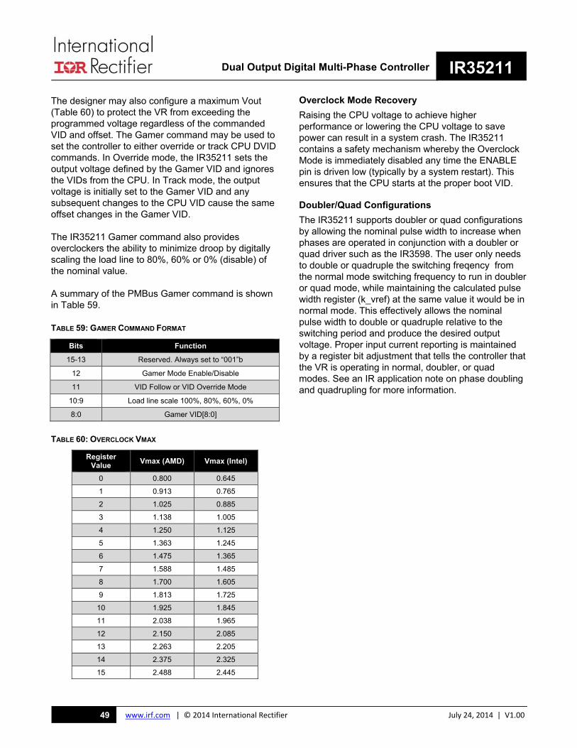
Dual Output Digital Multi-Phase Controller IR35211
www.irf.com | © 2014 International Rectifier July 24, 2014 | V1.0049
The designer may also configure a maximum Vout (Table 60) to protect the VR from exceeding the programmed voltage regardless of the commanded VID and offset. The Gamer command may be used to set the controller to either override or track CPU DVID commands. In Override mode, the IR35211 sets the output voltage defined by the Gamer VID and ignores the VIDs from the CPU. In Track mode, the output voltage is initially set to the Gamer VID and any subsequent changes to the CPU VID cause the same offset changes in the Gamer VID.
The IR35211 Gamer command also provides overclockers the ability to minimize droop by digitally scaling the load line to 80%, 60% or 0% (disable) of the nominal value.
A summary of the PMBus Gamer command is shown in Table 59.
TABLE 59: GAMER COMMAND FORMAT
Bits Function
15-13 Reserved. Always set to “001”b
12 Gamer Mode Enable/Disable
11 VID Follow or VID Override Mode
10:9 Load line scale 100%, 80%, 60%, 0%
8:0 Gamer VID[8:0]
TABLE 60: OVERCLOCK VMAX
Register Value
Vmax (AMD) Vmax (Intel)
0 0.800 0.645
1 0.913 0.765
2 1.025 0.885
3 1.138 1.005
4 1.250 1.125
5 1.363 1.245
6 1.475 1.365
7 1.588 1.485
8 1.700 1.605
9 1.813 1.725
10 1.925 1.845
11 2.038 1.965
12 2.150 2.085
13 2.263 2.205
14 2.375 2.325
15 2.488 2.445
Overclock Mode Recovery
Raising the CPU voltage to achieve higher performance or lowering the CPU voltage to save power can result in a system crash. The IR35211 contains a safety mechanism whereby the Overclock Mode is immediately disabled any time the ENABLE pin is driven low (typically by a system restart). This ensures that the CPU starts at the proper boot VID.
Doubler/Quad Configurations
The IR35211 supports doubler or quad configurations by allowing the nominal pulse width to increase when phases are operated in conjunction with a doubler or quad driver such as the IR3598. The user only needs to double or quadruple the switching freqency from the normal mode switching frequency to run in doubler or quad mode, while maintaining the calculated pulse width register (k_vref) at the same value it would be in normal mode. This effectively allows the nominal pulse width to double or quadruple relative to the switching period and produce the desired output voltage. Proper input current reporting is maintained by a register bit adjustment that tells the controller that the VR is operating in normal, doubler, or quad modes. See an IR application note on phase doubling and quadrupling for more information.

Dual Output Digital Multi-Phase Controller IR35211
www.irf.com | © 2014 International Rectifier July 24, 2014 | V1.0050
I2C PROTOCOLS
All registers may be accessed using either I2C or PMBus protocols. I2C allows the use of a simple format whereas PMBus provides error checking capability. Figure 50 shows the I2C format employed by the IR35211.
Figure 50: I2C Format
SMBUS/PMBUS PROTOCOLS
To access IR’s configuration and monitoring registers, 4 different protocols are required:
the SMBus Read/Write Byte/Word protocol with/without PEC (for status and monitoring)
the SMBus Send Byte protocol with/without PEC (for CLEAR_FAULTS only)
the SMBus Block Read protocol for accessing Model and Revision information
the SMBus Process call (for accessing Configuration Registers)
An explanation of which command codes and protocols are required to access them is given in Table 61. In addition, the IR35211 supports:
Alert Response Address (ARA)
Bus timeout (44.5ms)
Group Command for writing to many VRs within one command
SSlave
Address WCommand
Code Data Byte
1 7 1 8
S
1Slave
Address
7
W
1
A
A
A A P
8 1 111
Command Code
Data Byte High
8
A
8
1Data Byte
Low A
8 1
PEC*
81
A*
A P
1 1
PEC*
81
A*
BYTE
WORD…
S: Start Condition
A: Acknowledge (0')
N: Not Acknowledge (1')
Sr: Repeated Start Condition
P: Stop Condition
R: Read (1')
W: Write (0')
PEC: Packet Error Checking
*: Present if PEC is enabled
: Master to Slave
: Slave to Master
Figure 51: SMBus Write Byte/Word

Dual Output Digital Multi-Phase Controller IR35211
www.irf.com | © 2014 International Rectifier July 24, 2014 | V1.0051
Figure 52: SMBus Read Byte/Word
Figure 53: SMBus Send Byte
Figure 54: SMBus Block Read with Byte Count=1
Figure 55: SMBus Process Call to Write an IR Register
Figure 56: SMBus Process Call to Read an IR Register
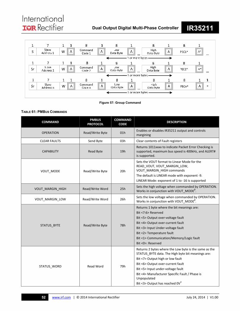
Dual Output Digital Multi-Phase Controller IR35211
www.irf.com | © 2014 International Rectifier July 24, 2014 | V1.0052
Figure 57: Group Command
TABLE 61: PMBUS COMMANDS
COMMAND PMBUS
PROTOCOL COMMAND
CODE DESCRIPTION
OPERATION Read/Write Byte 01h Enables or disables IR35211 output and controls margining
CLEAR FAULTS Send Byte 03h Clear contents of Fault registers
CAPABILITY Read Byte 19h Returns 1011xxxx to indicate Packet Error Checking is supported, maximum bus speed is 400kHz, and ALERT# is supported.
VOUT_MODE Read/Write Byte 20h
Sets the VOUT format to Linear Mode for the READ_VOUT, VOUT_MARGIN_LOW, VOUT_MARGIN_HIGH commands
The default is LINEAR mode with exponent ‐9.
LINEAR Mode: exponent of 1 to ‐16 is supported
VOUT_MARGIN_HIGH Read/Write Word 25h Sets the high voltage when commanded by OPERATION. Works in conjunction with VOUT_MODE2.
VOUT_MARGIN_LOW Read/Write Word 26h Sets the low voltage when commanded by OPERATION. Works in conjunction with VOUT_MODE
2.
STATUS_BYTE Read/Write Byte 78h
Returns 1 byte where the bit meanings are:
Bit <7:6> Reserved
Bit <5> Output over‐voltage fault
Bit <4> Output over‐current fault
Bit <3> Input Under‐voltage fault
Bit <2> Temperature fault
Bit <1> Communication/Memory/Logic fault
Bit <0>: Reserved
STATUS_WORD Read Word 79h
Returns 2 bytes where the Low byte is the same as the STATUS_BYTE data. The High byte bit meanings are:
Bit <7> Output high or low fault
Bit <6> Output over‐current fault
Bit <5> Input under‐voltage fault
Bit <4> Manufacturer Specific Fault / Phase is Unpopulated
Bit <3> Output has reached 0V3
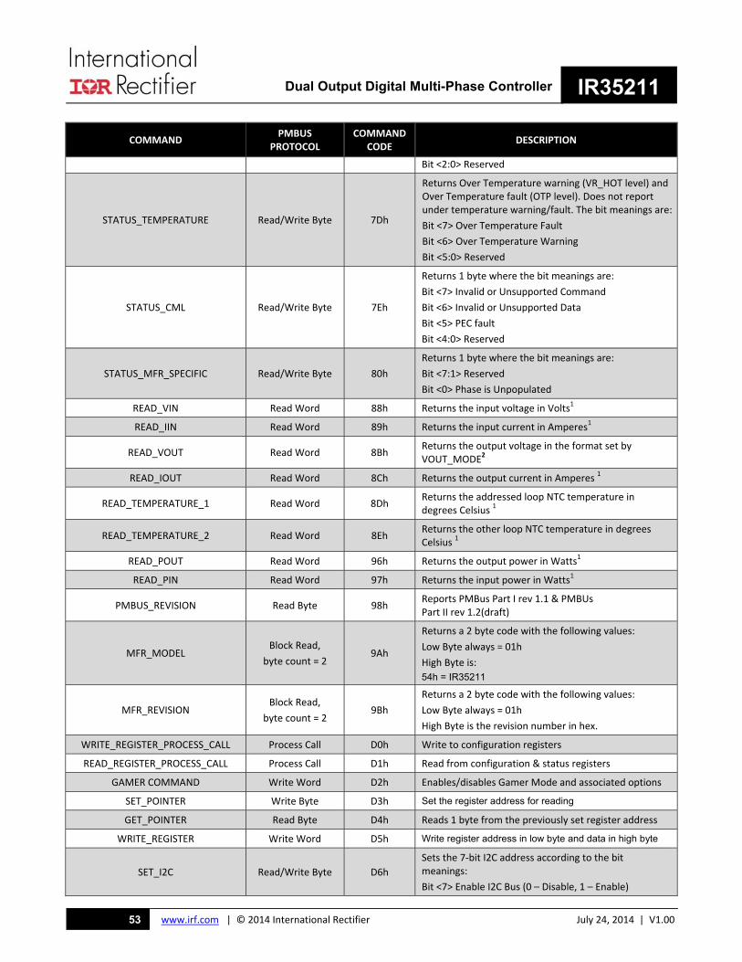
Dual Output Digital Multi-Phase Controller IR35211
www.irf.com | © 2014 International Rectifier July 24, 2014 | V1.0053
COMMAND PMBUS
PROTOCOL COMMAND
CODE DESCRIPTION
Bit <2:0> Reserved
STATUS_TEMPERATURE Read/Write Byte 7Dh
Returns Over Temperature warning (VR_HOT level) and Over Temperature fault (OTP level). Does not report under temperature warning/fault. The bit meanings are:
Bit <7> Over Temperature Fault
Bit <6> Over Temperature Warning
Bit <5:0> Reserved
STATUS_CML Read/Write Byte 7Eh
Returns 1 byte where the bit meanings are:
Bit <7> Invalid or Unsupported Command
Bit <6> Invalid or Unsupported Data
Bit <5> PEC fault
Bit <4:0> Reserved
STATUS_MFR_SPECIFIC Read/Write Byte 80h
Returns 1 byte where the bit meanings are:
Bit <7:1> Reserved
Bit <0> Phase is Unpopulated
READ_VIN Read Word 88h Returns the input voltage in Volts1
READ_IIN Read Word 89h Returns the input current in Amperes1
READ_VOUT Read Word 8Bh Returns the output voltage in the format set by VOUT_MODE
2
READ_IOUT Read Word 8Ch Returns the output current in Amperes 1
READ_TEMPERATURE_1 Read Word 8Dh Returns the addressed loop NTC temperature in degrees Celsius 1
READ_TEMPERATURE_2 Read Word 8Eh Returns the other loop NTC temperature in degrees Celsius 1
READ_POUT Read Word 96h Returns the output power in Watts1
READ_PIN Read Word 97h Returns the input power in Watts1
PMBUS_REVISION Read Byte 98h Reports PMBus Part I rev 1.1 & PMBUs Part II rev 1.2(draft)
MFR_MODEL Block Read,
byte count = 2 9Ah
Returns a 2 byte code with the following values:
Low Byte always = 01h
High Byte is:
54h = IR35211
MFR_REVISION Block Read,
byte count = 2 9Bh
Returns a 2 byte code with the following values:
Low Byte always = 01h
High Byte is the revision number in hex.
WRITE_REGISTER_PROCESS_CALL Process Call D0h Write to configuration registers
READ_REGISTER_PROCESS_CALL Process Call D1h Read from configuration & status registers
GAMER COMMAND Write Word D2h Enables/disables Gamer Mode and associated options
SET_POINTER Write Byte D3h Set the register address for reading
GET_POINTER Read Byte D4h Reads 1 byte from the previously set register address
WRITE_REGISTER Write Word D5h Write register address in low byte and data in high byte
SET_I2C Read/Write Byte D6h
Sets the 7‐bit I2C address according to the bit meanings:
Bit <7> Enable I2C Bus (0 – Disable, 1 – Enable)

Dual Output Digital Multi-Phase Controller IR35211
www.irf.com | © 2014 International Rectifier July 24, 2014 | V1.0054
COMMAND PMBUS
PROTOCOL COMMAND
CODE DESCRIPTION
Bit<6:0> 7‐bit I2C address
READ_EFFICIENCY Read Word D7h Reports the efficiency in %1
MASK_STATUS_WORD Read/Write Word D8h Masks STATUS_WORD bits.
MASK_TEMPERATURE Read/Write Byte D9h Masks STATUS_TEMPERATURE
MASK_CML Read/Write Byte DAh Masks STATUS_CML
MASK_MANUFACTURER Read/Write Byte DBh Masks STATUS_MFR_SPECIFIC
Note1 – 11-Bit Linear Data Format is used
Note2 – 16-Bit Linear Data Format is used Note3 – Asserts once when Vout = 0V. Must be cleared with CLEAR_FAULTS command.

Dual Output Digital Multi-Phase Controller IR35211
www.irf.com | © 2014 International Rectifier July 24, 2014 | V1.0055
11-BIT LINEAR DATA FORMAT
Monitored parameters use the Linear Data Format (Figure 58) encoding into 1 Word (2 bytes), where:
NYValue 2
Note N and Y are “signed” values. If, VOUT is set to linear format (by VOUT_MODE), then N is set by the VOUT_MODE command and only Y is returned in the data-field as a 16-bit unsigned number.
7 6 5 4 3 2 1 0 7 6 5 4 3 2 1 0
Figure 58: 11-bit Linear Data Format
16-BIT LINEAR DATA FORMAT
This format is only used for VOUT related commands (READ_VOUT, VOUT_MARGIN_HIGH, VOUT_MARGIN_LOW):
NYValue 2
Note N and Y are “signed” values. If, VOUT is set to linear format (by VOUT_MODE), then N is set by the VOUT_MODE command and only Y is returned in the data-field as a 16-bit unsigned number.
Figure 59: 16-bit Linear Data Format
Databyte High Databyte Low
N Y

Dual Output Digital Multi-Phase Controller IR35211
www.irf.com | © 2014 International Rectifier July 24, 2014 | V1.0056
MARKING INFORMATION
Figure 60: Package Marking
PACKAGE INFORMATION QFN 6x6mm, 40-pin
Figure 61: Package Dimensions
35211 AYWWX XXXXX
PIN 1
PART #
ASSEMBLER (A)/DATE(YWW)/MARKING CODE(X)
LOT CODE(ENG MODE - MIN 5 DIGITS OF EATI #)
(PROD MODE – 4 DIGIT SPN CODE)
Dual Output Digital Multi-Phase Controller IR35211
www.irf.com | © 2014 International Rectifier July 24, 2014 | V1.0057
ENVIRONMENTAL QUALIFICATIONS
Qualification Level Industrial
Moisture Sensitivity Level QFN package MSL2
ESD
Machine Model JESD22-A115-A
Human Body Model JESD22-A114-E
Charged Device Model JESD22-C101-C
Latch-up JESD78
RoHS Compliant Yes
† Qualification standards can be found at International Rectifier web site: http://www.irf.com †† Exceptions to AEC-Q101 requirements are noted in the qualification report.

Dual Output Digital Multi-Phase Controller IR35211
www.irf.com | © 2014 International Rectifier July 24, 2014 | V1.0058
Data and specifications subject to change without notice. This product will be designed and qualified for the Industrial market.
Qualification Standards can be found on IR’s Web site.
IR WORLD HEADQUARTERS: 233 Kansas St., El Segundo, California 90245, USA Tel: (310) 252-7105 TAC Fax: (310) 252-7903
Visit us at www.irf.com for sales contact information. www.irf.com