e cient self-timed interfaces for crossing clock …...e cient self-timed interfaces for crossing...
TRANSCRIPT
Efficient Self-Timed Interfaces for Crossing Clock Domains
by
Ajanta Chakraborty
B.Eng. Bhopal Engineering College, 2001
A THESIS SUBMITTED IN PARTIAL FULFILLMENT OF
THE REQUIREMENTS FOR THE DEGREE OF
Master of Science
in
THE FACULTY OF GRADUATE STUDIES
(Department of Computer Science)
We accept this thesis as conformingto the required standard
The University of British Columbia
August 2003
c© Ajanta Chakraborty, 2003

Abstract
With increasing integration densities, large chip designs are commonly partitioned into
multiple clock domains. While the computation within each individual domain may be
synchronous, the interfaces between these domains often use asynchronous methods. One
such approach is the STARI technique[Gre93, Gre95] where a self-timed FIFO compensates
for clock-skew between the sender and receiver. This dissertation presents implementations
of STARI where the FIFO consists of a single, handshaking stage. I start with the simplest
case where the sender and receiver operate at exactly the same frequency with an unknown
skew. I then generalize this design for links with clocks whose frequencies are rational
multiples of each other, clocks whose frequencies are closely matched, and arbitrary clocks.
In each of these cases, the STARI interface can exploit the stability of typical clocks to
achieve low latencies and negligible probabilities of synchronization failure using very simple
hardware. I have designed and tested a proof-of-concept chip fabricated with the TSMC
0.18µ CMOS process for the scenario where clocks of different domains are exactly matched
in frequency. The tests have demonstrated our claims about the skew tolerance of the design
and I am now in the process of designing the interface for further generalizations.
ii

Contents
Abstract ii
Contents iii
List of Figures v
Acknowledgements vii
1 Introduction 1
1.1 Multiple Clock Domain Scenarios . . . . . . . . . . . . . . . . . . . . . . . . 1
1.2 Contributions . . . . . . . . . . . . . . . . . . . . . . . . . . . . . . . . . . . 5
1.3 Overview . . . . . . . . . . . . . . . . . . . . . . . . . . . . . . . . . . . . . 6
2 Related Work 7
2.1 Skew and Jitter . . . . . . . . . . . . . . . . . . . . . . . . . . . . . . . . . . 7
2.2 Generation and Distribution of Clocks . . . . . . . . . . . . . . . . . . . . . 8
2.2.1 Clock Generation . . . . . . . . . . . . . . . . . . . . . . . . . . . . . 8
2.2.2 Clock Distribution . . . . . . . . . . . . . . . . . . . . . . . . . . . . 8
2.3 Skew Compensation Techniques . . . . . . . . . . . . . . . . . . . . . . . . . 12
2.3.1 GALS . . . . . . . . . . . . . . . . . . . . . . . . . . . . . . . . . . . 12
2.3.2 Synchronizing Buffers . . . . . . . . . . . . . . . . . . . . . . . . . . 16
2.3.3 Mesochronous Designs . . . . . . . . . . . . . . . . . . . . . . . . . . 16
iii

2.3.4 Plesiochronous Designs . . . . . . . . . . . . . . . . . . . . . . . . . 19
2.4 STARI . . . . . . . . . . . . . . . . . . . . . . . . . . . . . . . . . . . . . . . 21
3 MinSTARI: A Single Stage FIFO Interface 23
3.1 Description . . . . . . . . . . . . . . . . . . . . . . . . . . . . . . . . . . . . 25
3.2 Skew Tolerance . . . . . . . . . . . . . . . . . . . . . . . . . . . . . . . . . . 28
3.3 Initialization . . . . . . . . . . . . . . . . . . . . . . . . . . . . . . . . . . . 30
3.3.1 Maximum Robustness . . . . . . . . . . . . . . . . . . . . . . . . . . 31
3.3.2 Minimum Latency . . . . . . . . . . . . . . . . . . . . . . . . . . . . 34
4 Implementation and Test Results 36
4.1 Implementation . . . . . . . . . . . . . . . . . . . . . . . . . . . . . . . . . . 36
4.1.1 Design Overview . . . . . . . . . . . . . . . . . . . . . . . . . . . . . 36
4.1.2 Implementation Details . . . . . . . . . . . . . . . . . . . . . . . . . 37
4.2 Test Results . . . . . . . . . . . . . . . . . . . . . . . . . . . . . . . . . . . . 41
5 Generalizations: Rational, Close and Arbitrary Clocks 48
5.1 Rational Clock Frequency Multiples . . . . . . . . . . . . . . . . . . . . . . 48
5.2 Plesiochronous Interfaces . . . . . . . . . . . . . . . . . . . . . . . . . . . . 54
5.3 Arbitrary Clock Frequencies . . . . . . . . . . . . . . . . . . . . . . . . . . . 56
5.4 A FIFO Interface . . . . . . . . . . . . . . . . . . . . . . . . . . . . . . . . . 57
6 Conclusion 61
Bibliography 63
iv

List of Figures
1.1 Exactly Matched Clock scenario: A Chip Multiprocessor . . . . . . . . . . . 2
1.2 Rationally Related Clock scenario: A “typical” wireless SOC application . . 2
1.3 Nearly Matched Clock scenario . . . . . . . . . . . . . . . . . . . . . . . . . 2
2.1 Clock Generation Techniques . . . . . . . . . . . . . . . . . . . . . . . . . . 9
2.2 A GALS System . . . . . . . . . . . . . . . . . . . . . . . . . . . . . . . . . 13
2.3 A GALDS System . . . . . . . . . . . . . . . . . . . . . . . . . . . . . . . . 14
2.4 Communication Scheme with Resampling . . . . . . . . . . . . . . . . . . . 15
2.5 Mesochronous Timing . . . . . . . . . . . . . . . . . . . . . . . . . . . . . . 17
2.6 FIFO with Local Clock Control . . . . . . . . . . . . . . . . . . . . . . . . . 18
2.7 Globally Updated Mesochronous Method . . . . . . . . . . . . . . . . . . . 19
2.8 Plesiochronous Retiming . . . . . . . . . . . . . . . . . . . . . . . . . . . . . 20
2.9 Source Synchronous Communication . . . . . . . . . . . . . . . . . . . . . . 21
3.1 Interface as Latch with 2 clock inputs . . . . . . . . . . . . . . . . . . . . . 23
3.2 The Single Stage FIFO . . . . . . . . . . . . . . . . . . . . . . . . . . . . . . 24
3.3 Clock Timing For The FIFO . . . . . . . . . . . . . . . . . . . . . . . . . . 24
3.4 Latch Controller State Diagram . . . . . . . . . . . . . . . . . . . . . . . . . 27
3.5 A traditional C-element . . . . . . . . . . . . . . . . . . . . . . . . . . . . . 27
3.6 The Latch Controller . . . . . . . . . . . . . . . . . . . . . . . . . . . . . . . 28
3.7 Drifting Skew . . . . . . . . . . . . . . . . . . . . . . . . . . . . . . . . . . . 29
v

3.8 Five timing Scenarios . . . . . . . . . . . . . . . . . . . . . . . . . . . . . . 32
4.1 Design Setup . . . . . . . . . . . . . . . . . . . . . . . . . . . . . . . . . . . 36
4.2 LFSR . . . . . . . . . . . . . . . . . . . . . . . . . . . . . . . . . . . . . . . 38
4.3 Shift Register . . . . . . . . . . . . . . . . . . . . . . . . . . . . . . . . . . . 38
4.4 DAC . . . . . . . . . . . . . . . . . . . . . . . . . . . . . . . . . . . . . . . . 38
4.5 Modified Yuan-Svensson Latch . . . . . . . . . . . . . . . . . . . . . . . . . 39
4.6 en generation . . . . . . . . . . . . . . . . . . . . . . . . . . . . . . . . . . . 40
4.7 Receiver Shift Register . . . . . . . . . . . . . . . . . . . . . . . . . . . . . . 40
4.8 Error Detection Circuit . . . . . . . . . . . . . . . . . . . . . . . . . . . . . 41
4.9 Test Setup . . . . . . . . . . . . . . . . . . . . . . . . . . . . . . . . . . . . . 42
4.10 Skew Tolerance Window . . . . . . . . . . . . . . . . . . . . . . . . . . . . . 44
4.11 Phase Modulation Tolerance at 20MHz . . . . . . . . . . . . . . . . . . . . . 45
4.12 Phase Modulation Tolerance at 30MHz . . . . . . . . . . . . . . . . . . . . . 46
5.1 An Interface with Rational Clocks . . . . . . . . . . . . . . . . . . . . . . . 49
5.2 Exploiting Periodic jitter . . . . . . . . . . . . . . . . . . . . . . . . . . . . 50
5.3 A Miss Detector . . . . . . . . . . . . . . . . . . . . . . . . . . . . . . . . . 52
5.4 Receiver Frequency vs. Cycle Time constraint . . . . . . . . . . . . . . . . . 52
5.5 Interface for Nearly Matched Clocks . . . . . . . . . . . . . . . . . . . . . . 54
5.6 Interface for Arbitrary Clocks . . . . . . . . . . . . . . . . . . . . . . . . . . 56
5.7 Implementing a FIFO interface . . . . . . . . . . . . . . . . . . . . . . . . . 58
5.8 Symmetry in FIFO interface . . . . . . . . . . . . . . . . . . . . . . . . . . . 59
5.9 Timing scenarios with nearly full FIFO-R . . . . . . . . . . . . . . . . . . . 60
vi

Acknowledgements
This work has been possible through direct and indirect support of a variety of people. I
would like to sincerely thank my supervisor Dr. Mark Greentstreet for his unparalleled
guidance, encouragement and enthusiasm throughout my stay at UBC as a graduate stu-
dent. Being a total beginner in the field of VLSI design, the aid and help of colleagues and
friends was invaluable. Some of them being Brian Winters, for providing me the answers
to my unending questions and helping with design; Roberto Rosales for teaching me the
basics of chip testing and for relentlessly helping me with testing; Roozbeh for helping with
various CAD tools; and to the entire System-on-Chip lab of ECE department at UBC, for
giving me the opportunity to use their test lab and equipments.
I have no words to express my gratitude to my loving and doting parents who have
taught me to take on new challenges with vigor and also to my brother, Alexy, and my
sister, Jhinuk, without whom I would not have been here today. Thanks Rinkesh for always
being there for me and for the constant support and encouragement I have received from
you.
Ajanta Chakraborty
The University of British Columbia
August 2003
vii

Chapter 1
Introduction
1.1 Multiple Clock Domain Scenarios
As we move into very deep submicron technology, increasing integration densities and clock
frequencies drive designers to implement increasing numbers of on-chip clock domains. This
keeps the skew in clock and data to a small amount within a domain to ensure reliable
transfer of data. As tight timing tolerances cannot be guaranteed between timing do-
mains, communication between domains often takes place at a rate slower than the system
clock (e.g., one transfer for every two cycles of the clock) or using some kind of mixed syn-
chronous/asynchronous designs. Various multiple clock domain scenarios can be categorized
as:
1. Exactly matched clock frequencies
2. Rationally related clock frequencies
3. Nearly matched clock frequencies
4. Arbitrary clock frequencies
1. Exactly matched clock frequencies
In the scenario with exactly matched clocks, as shown in Figure 1.1 all the domains re-
1

1.1. Multiple Clock Domain Scenarios 2
CPU
I$ D$
CPU
I$ D$
CPU
I$ D$
CPU
I$ D$
L2$ L2$ L2$ L2$
Interconnect
Figure 1.1: Exactly Matched Clock scenario: A Chip Multiprocessor
AnalogRF ADC
DSP 2200 MHz
DSP 1500 MHz
LCD
Crypto
Memory
CPU 2CPU 1
Speakers
I/O Controller10 MHz
700 MHz 300 MHz 100 MHz
PLLs
Oscillator
Microphone
Keypad
Figure 1.2: Rationally Related Clock scenario: A “typical” wireless SOC application
Bridge
DDR
AGP
Infiniband
CPU
I$ D$L2$
Figure 1.3: Nearly Matched Clock scenario

1.1. Multiple Clock Domain Scenarios 3
ceive their clocks from the same source and are thus operating at exactly same frequency.
This is a typical situation in high-performance designs such as microprocessors for general
purpose computers. In these designs, clock and data skew [HN01] arise from a variety of
sources [BDM02]. First, scaling trends with decreasing feature sizes decrease gate delays
causing a corresponding increase in clock frequencies. For high performance designs, clock
frequencies are further increased by architectural trends favoring deeper pipelines with fewer
gates per pipeline stage.
Wire delays within a domain with a fixed number of transistors remain relatively con-
stant with scaling. For long wires, the performance gap with gate becomes very severe wih
shrinking feature size.
Thus, although within each domain the clock skews are relatively small allowing op-
eration at high clock rates, between clock domains, skews may be much larger. For ex-
ample two domains, which are at separate leaves of a clock tree distribution network,
might communicate with each other. Although circuits in these two domains may be
physically adjacent, there may be large, unpredictable phase differences between their
clock signals. Traditionally, designers target clock skews of about 10% of the clock pe-
riod [KB+01, RM+01, KA+01, IM02, KN+02]. Long wire delays and variations in buffer de-
lay make these targets challenging. Accordingly, designers resort to careful layout [BC+99]
and active skew compensation [TR+00]. Likewise, fabrication engineers reduce wiring de-
lays by deploying copper wires [Dav99] to lower resistance and low-k dielectrics [GA+02]
to reduce capacitance. These approaches come at a cost: circuit and layout approaches to
lowering clock skew often do so at an increase in circuit complexity and power consumption;
improvements in materials are limited by physical constants.
An alternate approach is to devise measures which compensate for skew when data is
transferred between domains. Source synchronous designs can be of great use in such sit-
uations. The designs presented are based on one such source synchronous communication
technique namely the STARI technique. Here a self timed FIFO is placed between the

1.1. Multiple Clock Domain Scenarios 4
communicating domains. The self-timed FIFO is used to compensate for skew between two
synchronous systems operating with a common clock. Section 2.4 describes STARI method
in greater detail.
2. Rationally related clock frequencies
In the scenario with rationally related clock frequencies, the clocks of the different domains
operate at frequencies that are rational multiples of each other. Figure 1.2 depicts a design
where different portions of the chip operate at different frequencies, and the various clocks
are derived from a common source. This commonly occurs in system-on-chip designs where
different IP blocks may be designed with different target clock frequencies or in multi-rate
digital-signal-processing designs. Although multiple clock frequencies are used, these fre-
quencies are exact rational multiples of each other, and these ratios are typically known in
advance or are determined by pre-designed operating modes of the design. Knowing the
exact relationship between the various clock frequencies enables the design of an interface
that operates with low latency and without synchronization.
3. Nearly matched clock frequencies
As shown in Figure 1.3, in the scenario with nearly matched clocks, the different domains
operate with independent sources that are closely matched in frequency. This occurs, for
example, in the design of network routers [KP+99] where each line card receives a bit
stream with an embedded clock from a different source. Although each stream comes with
its own clock, typically these clocks are very closely matched in frequency. For example,
ATM standards specify that bit rates be within one part per million of their nominal values.
4. Arbitrary clock frequencies
Finally in the scenario with arbitrary clock frequencies, the clocks are derived from in-
dependent sources and can have any arbitrary frequencies. While the frequencies may be

1.2. Contributions 5
arbitrary, typical synchronous designs use clocks that are very stable. Thus, the relationship
between the clock freuqncies change very slowly over time. This enables the design of an in-
terface where synchronization while necessary, is not critical to the latency of data transfers.
In this thesis, I present interfaces ensuring reliable communication in all of these multiple
clock domain scenarios. The designs described, use a self-timed FIFO which has a single
handshaking stage and thus is a minimalist version of the original design, namely STARI.
The essential observation behind my designs is that clocks for synchronous systems are
designed to be extremely stable. Thus, I can design STARI style interfaces that provide
moderate amounts of skew tolerance and dynamically compensate for any long-term drift
in skew or frequency. As described above, I present designs where the sender and receiver
operate at exactly the same frequency; at frequencies that are rational multiples of each
other; at closely matched frequencies; and at arbitrary, relatively stable frequencies. In the
remainder of the thesis, I show that these designs are small and can operate at high clock
frequencies with low latencies.
1.2 Contributions
In this thesis, I show that, multiple clock domains with exactly matched, rationally related,
nearly matched and arbitrary frequencies can communicate reliably and efficiently using a
single stage FIFO that offers nearly two clock periods of skew tolerance.
The contributions of this dissertation can be summarized as:
• Detailed study of the minimalist version of the STARI design along with an analysis
of its skew tolerance.
• A novel initialization mechanism that achieves maximum robustness.
• Designing a proof-of-concept chip implementing the minSTARI(described in Chap-
ter 3) design and sufficient test circuitry to verify its functionality.
1.3. Overview 6
• Detailed analysis and design of extensions of the basic design to apply to the more
general multiple clock domain scenarios.
1.3 Overview
The document is organized as follows:
I begin with a brief description of clock skew and jitter in digital designs and why it poses
a problem with shrinking die sizes and increasing transistor density. Next a variety of
techniques are described which have been used or suggested to handle clock skew, including
the STARI method which this research extends.
Next I describe a minimalist version of the original STARI method, minSTARI, in
Chapter 3 which can achieve a skew tolerance of almost two clock periods. Thus, minSTARI
forms the solution for exactly matched clock scenario where clocks of different domains are
operating at the same frequency. Chapter 4 describes a proof-of-concept chip demonstrating
the operation of the design along with the test results obtained.
In the further generalizations of the basic idea, additional circuitry is used to reduce
each scenario to the exactly matched clock frequencies scenario, and then minSTARI is used
to handle the skew. For example, the design for rationally related clock frequencies scenario
generates a rational approximation of clocks to reduce the design to matched frequency
scenario. Similarly the closely matched and arbitrary clock frequencies scenario also use
combination of various other techniques to achieve the same objective. The generalizations
are explained in Chapter 5.
Chapter 2
Related Work
2.1 Skew and Jitter
Skew can be viewed conceptually as the uncertainty in the timing of clock or data. More
specifically clock skew can be defined as the difference in time between simultaneous tran-
sitions of the clock within a system [Kat98] which is introduced by the clock distribution
system. Clock jitter can be defined as short-term variations of the significant instants of
the clock signal from its ideal position in time. Various factors can contribute to clock
skew[BC+99], such as:
1. Process variation between transistors: each buffer stage introduces uncertainties due to
process variations. To reduce skew, designers can reduce the number of buffer stages in the
clock distribution network.
2. Variation in parameters of the wires used: long wires introduce uncertainties and thus,
should be avoided.
3. Different sizing of each buffering stage according to the load it has to drive.
4. Presence of adjacent wires and the amount of switching activities between them.
5. Inductive reactances of the wires.
6. And finally, variations in factors such as temperature, power supply voltage etc.
Skew is becoming a major limiting factor in increasing the global clock frequency. Com-
7

2.2. Generation and Distribution of Clocks 8
pensating skew generally involves introducing complicated architectures or faster logic.
2.2 Generation and Distribution of Clocks
2.2.1 Clock Generation
Three standard approaches to clock generation are Phase Locked Loops(PLLs), off chip
oscillators and Delay Locked Loops(DLLs).
A. PLL based design
In the PLL based designs, a low speed reference clock is distributed throughout the chip
and PLLs are used to obtain different multiples of the base frequency as required by various
sub-components. Clock jitter in this case is typically 5% of the clock cycle[BC+99].
B. Off-Chip Oscillator
In an off-chip oscillator, as the name suggests, an off-chip oscillator is used to generate very
stable clock signals. Synchronizing the clock signal with the system becomes a difficult
task but can have very low clock jitter amounting to as little as 1% of the clock cycle to a
maximum of 5% [BC+99].
C. DLL based design
In DLL based designs, the local clock is delayed sufficiently to line up with the edge of system
clock and thus can be used for latency correction or introducing a desired phase difference
if needed. DLL based designs form an attractive alternative to PLL based designs due to
their better jitter performance, inherent stability and simpler design but are difficult to use
for frequency synthesis [SH97].
2.2.2 Clock Distribution
The topology and technique for clock distribution plays a very important part in determining
skew and jitter and for the overall performance of the system. Thus, much effort is spent
in designing and optimizing clock networks which can balance factors such as skew and

2.2. Generation and Distribution of Clocks 9
Low PassFilter Controlled
Voltage
OscillatorDetectorPhase
Divide By n
a. PLL based design b. Off−Chip Oscillator c. DLL based design
sync. LocalDomainOscillator
System Clock
matchingdelay Local
DomainLocal Clock
Figure 2.1: Clock Generation Techniques
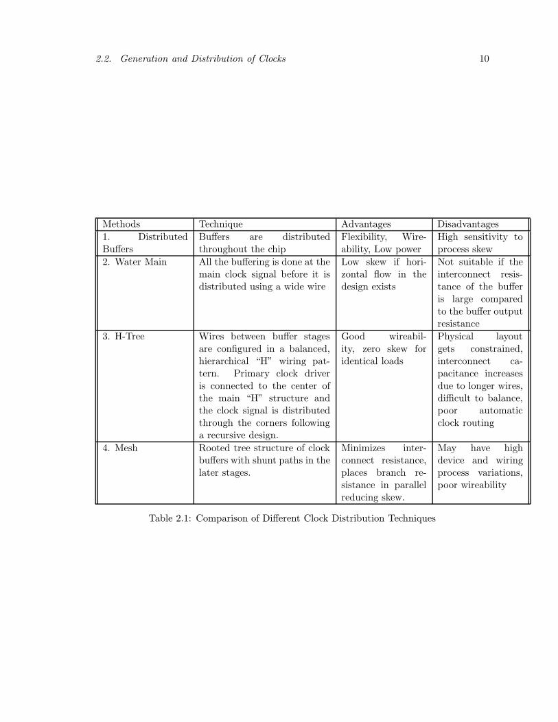
clock tree delays. Table 2.1 gives a comparison of some of the standard clock distribution
techniques:
Example Implementations of Clock Networks
1. DEC Alpha series: The design is primarily based on mesh or grid techniques where
wires are cross-connected with vertical and horizontal straps in a mesh pattern which keeps
the clocks in phase across the whole chip. The Alpha microprocessors require that a sub-
stantial capacitive load be driven at high speed along with maintaining a fast edge rate.
Thus, in the earlier designs five levels of buffering configured as a tree were used. For ex-
ample,the Alphaserver 4100 clock distribution system uses a combination of both balanced
H-Tree and shared output tree to distribute the clock signal [Dam97]. The balanced H-Tree
takes care of the fixed load blocks, whereas the shared output tree is used where various
module configurations could alter clock loading. Later for a 600 MHz Alpha processor, a
hierarchy of clocks was used where a gridded global clock with windowpane arrangement
of final distributed drivers was used to lower the skew[BB98]. More clocks were derived
out of these to provide more flexibility. Thus, a very complicated structure was adopted
to enhance performance and save power. Similarly, for a processor running at 1.2 GHz,
the difficulties in distributing clocks over large areas using low resistance grids are avoided
by moving away from single chip-wide clock distribution to multiple phase locked clocks
controlling different components of the chip for better skew and jitter control. Networks
of various kinds ranging from P-shaped grids, rectangular X-trees to partial H-trees were
2.2. Generation and Distribution of Clocks 10
Methods Technique Advantages Disadvantages
1. DistributedBuffers
Buffers are distributedthroughout the chip
Flexibility, Wire-ability, Low power
High sensitivity toprocess skew
2. Water Main All the buffering is done at themain clock signal before it isdistributed using a wide wire
Low skew if hori-zontal flow in thedesign exists
Not suitable if theinterconnect resis-tance of the bufferis large comparedto the buffer outputresistance
3. H-Tree Wires between buffer stagesare configured in a balanced,hierarchical “H” wiring pat-tern. Primary clock driveris connected to the center ofthe main “H” structure andthe clock signal is distributedthrough the corners followinga recursive design.
Good wireabil-ity, zero skew foridentical loads
Physical layoutgets constrained,interconnect ca-pacitance increasesdue to longer wires,difficult to balance,poor automaticclock routing
4. Mesh Rooted tree structure of clockbuffers with shunt paths in thelater stages.
Minimizes inter-connect resistance,places branch re-sistance in parallelreducing skew.
May have highdevice and wiringprocess variations,poor wireability
Table 2.1: Comparison of Different Clock Distribution Techniques

2.2. Generation and Distribution of Clocks 11
used[XB+01].
2. IBM S/390 Microprocessor: This is a 400 MHz CMOS microprocessor which
primarily uses tree-like structures. A single clock is distributed from a centrally located
on-chip PLL through a single buffer to 580 distribution points[RJDC98]. The distribution
is achieved in two levels of balanced H-like trees. The first level tree distributes the central
clock to nine buffers which are then further distributed in the second level. Using a small
number of large buffers reduces skew and jitter from on-chip process and variations but
results in more complicated wiring networks.
3. Intel “Itanium” Microprocessor: This is another microprocessor designed for
running at GHz level frequency. It primarily uses programmable deskew circuits while
supporting local optimization of the clock distribution network[RT00]. The architecture
consists of three components: a balanced tree for distributing the global clock, multiple
deskew buffers with balanced tree structures driving the regional clock grids, and multi-
ple local clock buffers tapping these regional grids. A reference clock is also distributed
throughout the chip for phase correction.
4. Other techniques: The signal integrity problems due to clock jitter, clock skew
and signal reflection have motivated researchers to look into alternative methods of in-
terconnection. Thus, apart from digital interconnect techniques, optical interconnect and
RF and microwave interconnect have also appeared in the picture. Optical interconnect
have lower power consumption at very high frequencies and good signal integrity properties
but are bulky, expensive and difficult to fabricate[RWW+02]. Two major kinds of optical
interconnects are based on either free-space technology or guided-wave technology. The in-
termediate technology between metal-based and optical interconnect is RF and microwave
interconnects. My work is focused on the existing approach i.e. digital interconnects.
In summary, various methods have been devised for proper clock generation and distri-
bution which can lead to stable clock signals and reduced skew. However, in most large VLSI
designs, long wires and large numbers of components create large interconnect impedances.

2.3. Skew Compensation Techniques 12
Moreover, factors including variation in temperature, power supply voltage etc., introduce
an arbitrary amount of skew in the signals both along the clock and data path. Thus, it
becomes necessary to adopt some kind of clock skew compensation technique.
2.3 Skew Compensation Techniques
Given the challenges of transmitting signals between clock domains, researchers have ex-
plored a variety of asynchronous solutions. These range from building completely asyn-
chronous chips [MB+89, ML+97, FEG00, RB+01] to various combinations of synchronous
and asynchronous modules in the same design. Here I, focus on the latter approach. The
various methods for combining asynchronous and synchronous modules vary according to
the requirements that are placed on the clock. At one extreme, GALS (i.e. “Globally
Asynchronous, Locally Synchronous”) designs make very minimal assumptions about clock
timing, effectively turning clocks into bundled completion signals and adding handshaking
to clock generation [Cha84]. At the other extreme, “mesochronous” and “plesiochronous”
methods rely on exact or nearly exact frequency matching of the clocks [Mes90]. Be-
tween these two extremes, synchronizing buffers allow each domain to operate with its own
clock, but make minimal assumptions about the relationships between these clocks. My
approaches fall squarely in the mesochronous and plesiochronous camps. I summarize these
various approaches below.
2.3.1 GALS
As originally proposed by Chapiro [Cha84], GALS (i.e. “Globally Asynchronous, Locally
Synchronous”) designs use stoppable clocks to allow synchronous modules to communicate
using asynchronous protocols. Each synchronous domain has its own clock generator that
consists of a ring oscillator with a handshaking stage. When domain X has a value to send
to domain Y, X outputs the value, sends a request to Y and stalls its clock until it receives

2.3. Skew Compensation Techniques 13
controllerPort
controllerPort
LocalClock
Generator
SynchronousLocally
Block
Port Port
WrapperAsynchronous
Figure 2.2: A GALS System
an acknowledgement. Likewise, when domain Y is prepared to receive a value from domain
X, it stalls its clock, waits for a request from X, latches the value, sends an acknowledgement
to X and restarts its own clock.
Yun and Donohue [YD96] extended Chapiro’s approach by adding a mutual-exclusion
element to the ring oscillator. This allows each locally synchronous block to continue oper-
ating while polling for input from its neighbours. The mutual exclusion element delays the
next clock event, if needed, to allow metastability [CM73] arising from the polling to resolve.
Yun and Donohue’s approach allows GALS designs to be very flexible, and their methods
have been extended by several research groups, e.g. [MVF00, SM00, MT+02, SPL02]. Their
design is not metastability free but no clock events occur while it is being resolved which
prevents the communicating domains from accepting incorrect data. However, pausing or
stretching the clock increases latency in the system.
Chattopadhyay and Zilic [CZ02] extended this work further by designing a GALDS sys-
tem which stands for Globally Asynchronous Locally Dynamic System as shown in Figure
2.3. GALDS is based on the observation that dynamically switching clock frequencies is an
effective method of saving power. Thus instead of generating a fixed frequency clock signal
for the local domains, it uses a local clock controller which dynamically varies the clock fre-
quency according to the requirement. The design uses a ‘unidirectional synchronizer, which
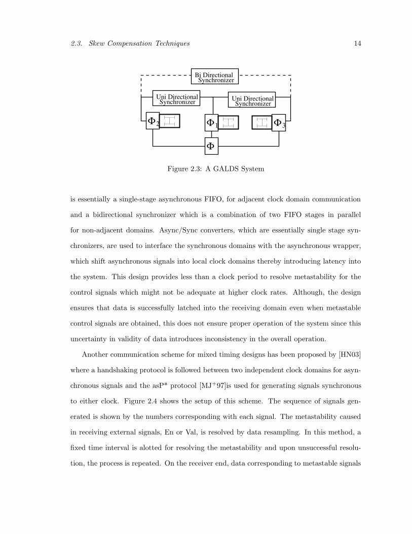
2.3. Skew Compensation Techniques 14
Uni DirectionalSynchronizer
Bi DirectionalSynchronizer
Φ1 Φ3Φ2
Φ
Uni DirectionalSynchronizer
Figure 2.3: A GALDS System
is essentially a single-stage asynchronous FIFO, for adjacent clock domain communication
and a bidirectional synchronizer which is a combination of two FIFO stages in parallel
for non-adjacent domains. Async/Sync converters, which are essentially single stage syn-
chronizers, are used to interface the synchronous domains with the asynchronous wrapper,
which shift asynchronous signals into local clock domains thereby introducing latency into
the system. This design provides less than a clock period to resolve metastability for the
control signals which might not be adequate at higher clock rates. Although, the design
ensures that data is successfully latched into the receiving domain even when metastable
control signals are obtained, this does not ensure proper operation of the system since this
uncertainty in validity of data introduces inconsistency in the overall operation.
Another communication scheme for mixed timing designs has been proposed by [HN03]
where a handshaking protocol is followed between two independent clock domains for asyn-
chronous signals and the asP* protocol [MJ+97]is used for generating signals synchronous
to either clock. Figure 2.4 shows the setup of this scheme. The sequence of signals gen-
erated is shown by the numbers corresponding with each signal. The metastability caused
in receiving external signals, En or Val, is resolved by data resampling. In this method, a
fixed time interval is alotted for resolving the metastability and upon unsuccessful resolu-
tion, the process is repeated. On the receiver end, data corresponding to metastable signals

2.3. Skew Compensation Techniques 15
SENDER
Clk1
ER
CEIVER
Clk2
Rst(1)
Data
Ack(1/5)
Val(4)
Ack(1/5)
Req(3)
En(2)
Req(3) ValGen
EnGen
Figure 2.4: Communication Scheme with Resampling
is overwritten by data of a successful attempt.
GALS makes minimal assumptions about clock stability; in fact, GALS discards the
stability and low-jitter of clocks that are the hallmarks of synchronous design. The frequency
stability of traditional clocks allows us to determine the relative phase of two independent
clocks thousands or more of cycles in advance. As I describe in sections 5.2 and 5.3, this
predictability enables moving metastability off the latency critical paths in my designs.
Also, in GALS designs, since a logic signal with a low drive, controls the clock which has
a very high fan-out. Thus, a high amount of amplification is required before the signal is
fed into the clock control circuit which introduces latency. Jitter is the variation in the
time between successive clock events. This variation directly degrades the performance of
synchronous designs, and clock pausing exacerbates jitter. After pausing a clock, the first
edge through the ring oscillator and clock buffer will propagate slower than subsequent
events [WGG02]. The loss of long-term timing predictability and the increase of jitter are
consequences of the GALS approach of converting synchronous designs into asynchronous
ones. In this thesis, I show that more efficient designs are achieved by letting synchronous
modules be synchronous and using simple asynchronous interfaces to compensate for clock-
skew and other timing uncertainties.
2.3. Skew Compensation Techniques 16
2.3.2 Synchronizing Buffers
The next step in our taxonomy allows independent, free-running clocks in each domain and
makes minimal assumptions about the timing relationships between them. A common rule-
of-thumb for design specifies the use of two or three synchronizing latches whenever a clock
domain is crossed [JG93, Chapter 3.11.4]. [JG93] also expresses the clock-to-output delay
of a latch as a function of the difference of the setup and the critical switching time of the
latch. This motivates increasing the number of stages of the synchronizer with increasing
clock rates. Thus, for high-performance designs with a small number of gate-delays per
clock period, even longer chains may be needed to achieve acceptably low probabilities of
failure. Seizovic [Sei94] recognized that these synchronizations can be pipelined allowing
high throughput even when the time for reliable synchronization is many clock periods.
Chelcea and Nowick [CN01] further optimized this approach by noting that synchronizations
are only needed for the receiver when the buffer is close to empty and only needed for the
sender when the buffer is close to full. All of these approaches still incur worst-case latency
due to either buffering latency when the buffer is not nearly empty or due to synchronization
latency when the buffers are nearly empty. Iyer and Marculescu [IM02] evaluated the
performance of a superscalar microprocessor design decomposed using Chelcea and Nowick’s
FIFOs. Superscalars are particularly sensitive to latency, and Iyer and Marculescu found
that the performance penalties arising from the added latency outweighed the power savings
for the design that they considered.
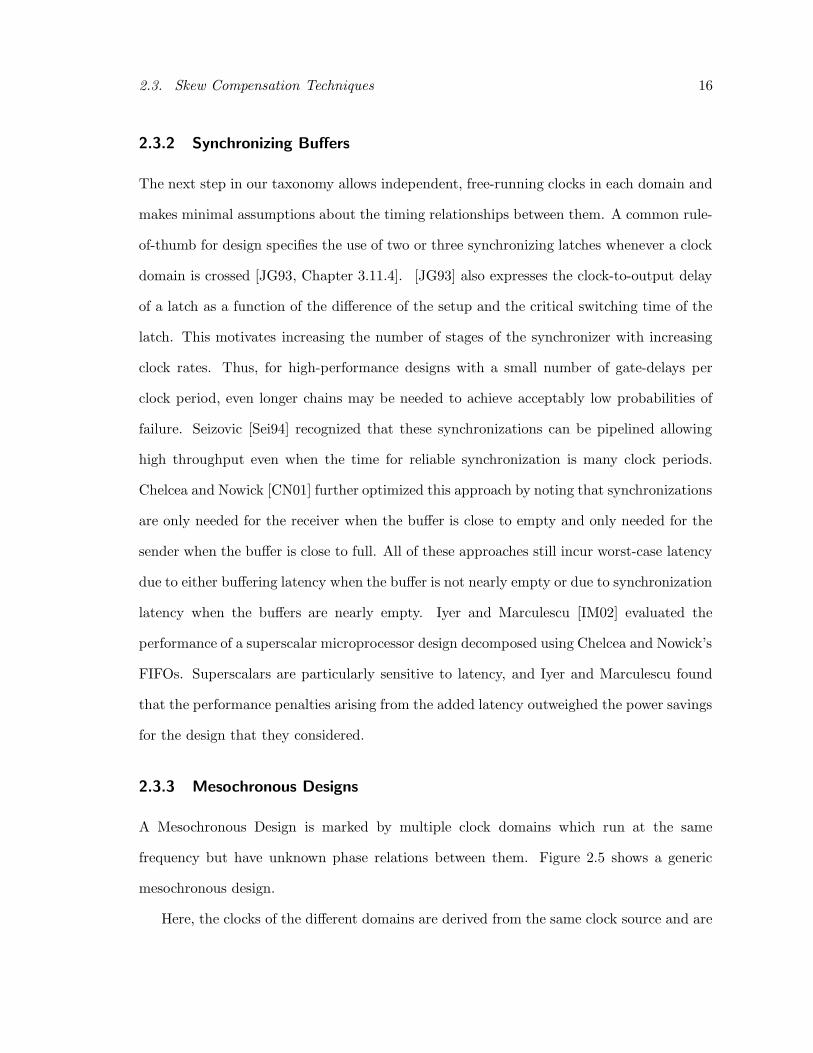
2.3.3 Mesochronous Designs
A Mesochronous Design is marked by multiple clock domains which run at the same
frequency but have unknown phase relations between them. Figure 2.5 shows a generic
mesochronous design.
Here, the clocks of the different domains are derived from the same clock source and are
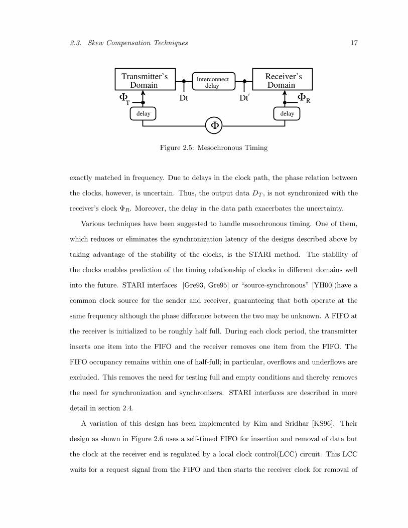
2.3. Skew Compensation Techniques 17
ΦT
delay
ΦR
delay
Φ
Interconnectdelay
Transmitter’sDomain Domain
Receiver’s
Dt Dt
Figure 2.5: Mesochronous Timing
exactly matched in frequency. Due to delays in the clock path, the phase relation between
the clocks, however, is uncertain. Thus, the output data DT , is not synchronized with the
receiver’s clock ΦR. Moreover, the delay in the data path exacerbates the uncertainty.
Various techniques have been suggested to handle mesochronous timing. One of them,
which reduces or eliminates the synchronization latency of the designs described above by
taking advantage of the stability of the clocks, is the STARI method. The stability of
the clocks enables prediction of the timing relationship of clocks in different domains well
into the future. STARI interfaces [Gre93, Gre95] or “source-synchronous” [YH00])have a
common clock source for the sender and receiver, guaranteeing that both operate at the
same frequency although the phase difference between the two may be unknown. A FIFO at
the receiver is initialized to be roughly half full. During each clock period, the transmitter
inserts one item into the FIFO and the receiver removes one item from the FIFO. The
FIFO occupancy remains within one of half-full; in particular, overflows and underflows are
excluded. This removes the need for testing full and empty conditions and thereby removes
the need for synchronization and synchronizers. STARI interfaces are described in more
detail in section 2.4.
A variation of this design has been implemented by Kim and Sridhar [KS96]. Their
design as shown in Figure 2.6 uses a self-timed FIFO for insertion and removal of data but
the clock at the receiver end is regulated by a local clock control(LCC) circuit. This LCC
waits for a request signal from the FIFO and then starts the receiver clock for removal of

2.3. Skew Compensation Techniques 18
Transmitter Receiver
Self−Timed FIFO
Clock Gen
LCC
clk clk
data
c1
cn
data
ack
done
lclk
Figure 2.6: FIFO with Local Clock Control
data. Synchronization is required for the first datum and subsequent data is removed every
clock cycle. Thus, instead of using phase detectors, this method relies on adjusting the
data arrival time so that it is synchronized at the receiver end. The LCC is implemented
through a series of three C-elements(described in Section 3.1), and metastability is resolved
through a comparator. This method could suffer from the disadvantages of pausing clocks
similar to GALS and could have restrictions in high performance designs [MS01]. Also the
modifications required in case of multiple domains communicating with the receiver are
unclear.
A second variation is provided by[S03] called Globally Updated Mesochronous(GUM)
Design. Here instead of using a FIFO, clocks with adjustable delays are used in each syn-
chronous domain. A calibration process determines the ideal phase offset between the clocks
by measuring the round trip latency of the data path between the communicating domains.
In particular it starts from an arbitrary, initial operating point and slowly increases the
delay of a clock signal until it enters a failure zone with respect to the other clock. Once
the window of operation is determined, the clock pulse is positioned in the center of the
window. This calibration process resembles the dynamic initalization process described in
section 3.3.1 and 3.3.2. The difference is that the GUM method can not dynamically ac-
count for skew, which our method can, and thus for factors like variations in temperature,

2.3. Skew Compensation Techniques 19
delayadjustable
delayadjustable
Φ
Domain 1 Domain 2
Figure 2.7: Globally Updated Mesochronous Method
power supply noise etc.. Furthermore, the initialization process has to be repeated many
times to account for any dynamic skew. Moreover, the additional complexity of maintaining
an adjustable delay and repeating the careful measurement process several times with each
clock can be quite tedious.
There has also been an effort to apply mesochronous techniques to on-chip networks
[Wik03]. In this technique, the transmitter sends its data and a strobe signal which is kept
at half the frequency of the transmitter’s clock. The receiver multiplies the strobe signal
to generate the clock signal and latches the incoming data using this generated clock. A
phase comparator compares the incoming data at every cycle with the receiver’s clock and
then selects either the receiver clock signal or the receiver clock delayed by half a clock
period, to trigger a second latch which generates the final data for the receiver’s domain.
The comparator requires synchronization and may take arbitrary long time to resolve if
both the selection signals are equally good.
My solution for mesochronous designs is a STARI-based technique and is described in
more detail in the subsequent chapters.
2.3.4 Plesiochronous Designs
In plesiochronous designs, the sender’s and receiver’s clocks are generated separately but
are closely matched in frequency [Mes90, DDX95]. Accordingly, the relative phase between
the sender and receiver changes very slowly.

2.3. Skew Compensation Techniques 20
Receiverdelay/2 Π
MUX
T RΦ Φ
Flip Region Detector
Transmitter
Figure 2.8: Plesiochronous Retiming
Rather than detecting FIFO-full and FIFO-empty conditions, a plesiochronous interface
can include circuitry to detect FIFO-nearly-full or FIFO-nearly-empty conditions. These
conditions can be synchronized to the appropriate clock domain with extremely reliable,
high-latency synchronizers.
[DDX95] is based on data retiming where two versions of transmitter’s data, original and
delayed by half a clock period, are maintained. Based on the timing of the receiver’s signal,
dynamic mode switching occurs choosing the one which has more tolerance for frequency
mismatch. This method is similar to my work in that it also separates synchronization from
the latency critical path. In [DDX95], the transmitter is always kept at a slower pace by
introducing non-data items which constitutes of a fixed percentage of total bandwidth to
avoid overflow of data and leads to performance degradation by 2δf . This method requires
real time switching between different input modes and hence provides smaller interval to
complete switching without duplicating or missing data. It also requires previous knowledge
of data and nondata elements for successful switching.
In my method, real-time switching is avoided by using “near miss” detectors as described
in Section 5.2 that enable us to predict the overflow and underflow well before they would
actually occur. As an example, consider the case where the sender and receiver clocks are
guaranteed to be matched to within 1 ppm (a typical requirement for high-speed networks).
Let a “near-empty” detector report the condition that data from the transmitter arrived
such that it was available for removal from the FIFO less than 10% of a clock period before
the actual removal. With the close clock matching, at least 100,000 clock cycles will elapse
2.4. STARI 21
. .. D Q D Q . ..
ΦT’
insertdata_in data_out
remove
FIFO
Φ
ΦT
unknowndelay
unknowndelay
ΦR
sender’s domain receiver’s domain
forwarded clk
data T’D
Figure 2.9: Source Synchronous Communication
before an underflow occurs! Thus, a ten or more stage synchronizer can be used to report
this “near-empty” condition to the receiver without risk of underflow. The receiver can
then skip removing a datum in a subsequent clock cycle, and it will be at least one-million
clock cycles until the next near-empty condition occurs. While the synchronization path
for flow control signals can have very high latency in a plesiochronous design, the latency
of the data path can be kept very low. In section 5.2 we show how our designs can be
used to implement plesiochronous interfaces. Section 5.3 generalizes this to interfaces with
arbitrary, stable clocks.
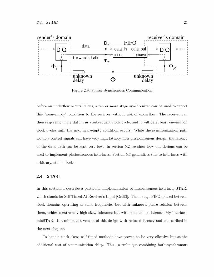
2.4 STARI
In this section, I describe a particular implementation of mesochronous interface, STARI
which stands for Self Timed At Receiver’s Input [Gre93]. The n-stage FIFO, placed between
clock domains operating at same frequencies but with unknown phase relation between
them, achieves extremely high skew tolerance but with some added latency. My interface,
minSTARI, is a minimalist version of this design with reduced latency and is described in
the next chapter.
To handle clock skew, self-timed methods have proven to be very effective but at the
additional cost of communication delay. Thus, a technique combining both synchronous

2.4. STARI 22
and asynchronous approaches can be more effective than either. STARI is such a combi-
nation where an n-stage FIFO is placed between the communicating domains. Figure 2.9
describes a STARI interface. Both the transmitter and receiver derive their clocks, ΦT and
ΦR respectively, from the same clock generator Φ. The delays in the path from clock gen-
erator to any clock signal are assumed to be arbitrary. The transmitter’s domain forwards
both its data and its clock ΦT ′ to the FIFO. Because ΦT ′ and ΦR are exactly matched
in frequency, the insertion rate of the FIFO is same as the removal rate of the FIFO. If
the FIFO is initialized to be roughly half full, then throughout operation, the capacity of
the FIFO remains roughly half full. Thus, the need to check for overflow and underflow is
avoided. The FIFO can be implemented with individual C-elements or using simple latches
acting as buffers. Thus STARI offers clear advantages over purely synchronous or purely
asynchronous systems because it does not require the absolute synchronization of purely
synchronous methods nor does it require the explicit flow control mechanism of purely
asynchronous ones.
In this thesis, I present both specializations and generalizations of the original STARI
work. In Chapter 3 a specialization of STARI is described by focusing on the case where
the FIFO consists of a single stage. Such an implementation provides nearly two clock
periods of skew tolerance. By optimizing for the single-stage case, I obtained very simple
interfaces between the edge-triggered conventions common in synchronous design and the
handshaking communication that is characteristic of self-timed designs. I then generalize
STARI to relax the requirement of exactly matched clocks at the sender and receiver. I
present interfaces where the sender and receiver clock frequencies are rational multiples of
each other(Section 5.1), closely matched(Section 5.2), and arbitrary(Section 5.3). All of
these designs exploit the long-term stability of clocks to obtain simple interfaces with small
latencies.

Chapter 3
MinSTARI: A Single Stage FIFO
Interface
This chapter describes a simple implementation of STARI communication where the FIFO
has a single stage. As shown in Figure 3.2, the FIFO consists of a single latch, and a latch
controller that generates a clock for this latch based on the clocks from the transmitter and
receiver. To the user, this FIFO appears as a latch with two clock inputs(Figure 3.1).
In this chapter and the next, it is assumed that the transmitter and receiver operate at
exactly the same frequency; only the relative phase difference is unknown. This is easily
achieved if both of their clocks are derived from a common source.
ΦT ΦR
D Q receiverdata todata from
transmitter
Figure 3.1: Interface as Latch with 2 clock inputs
23

24
latch−Rlatch−Xlatch−TQD
ΦT ΦR
QD data_out
Φ
latch controller
X
QDdata_in
single−stage FIFOtransmitter receiver
Figure 3.2: The Single Stage FIFO
ΦR
TΦ
st
ΦX
TRδ
ht
RTδ
hthtst st
γTR
γRT
OK OKFigure 3.3: Clock Timing For The FIFO

3.1. Description 25
3.1 Description
Figure 3.3 depicts the timing for the single-stage FIFO. For simplicity, I assume that the
latches are positive-edge-triggered. My design easily generalizes to other latching styles.
For proper operation, the latch controller must generate ΦX so as to satisfy the set-up and
hold requirements of latch-X and latch-R. To satisfy the requirements of latch-X, the rising
edge of ΦX must occur at least tset−up +tprop (abbreviated ts in the figure) after the previous
ΦT event, and at least thold − tprop (abbreviated th in the figure) before the next ΦT event,
where tset−up , thold , and tprop denote the set-up and hold times and propagation delay of
the latches respectively. To satisfy the requirements of latch-R, the rising edge of ΦX must
occur at least thold − tprop after the previous ΦR event, and at least tset−up + tprop before the
next ΦR event. The “exclusion” regions corresponding to these requirements are indicated
by cross-hatched regions for ΦX in Figure 3.3.
There are two windows of opportunity for generating ΦX : a rising edge of ΦX may occur
between a rising edge of ΦT and the subsequent rising edge of ΦR, or between the rising
edge of ΦR and the subsequent rising edge of ΦT . I refer to these scenarios according to the
last event (ΦT or ΦR) that occurs prior to each ΦX event. Thus, if ΦX occurs after a ΦT
event but before the next ΦR event, I refer to this situation as “transmitter-last”. Likewise,
I use “receiver-last” to refer to the other case. In Figure3.3, δTR denotes the time from the
rising edge of ΦT to the next rising edge of ΦR. Likewise, δRT denotes the time from the
rising edge of ΦR to the next rising edge of ΦT . Let P denote the clock period. Now, let
γTR denote the width of the window of opportunity for the transmitter-last scenario, and

3.1. Description 26
γRT denote the width of the window of opportunity for the receiver-last case. We have:
γTR = δTR − 2(tset−up + tprop)
γRT = δRT − 2(thold − tprop)
⇒ γTR + γRT = δTR + δRT − 2(tset−up + thold )
= P − 2(tset−up + thold )
⇒ max(γTR, γRT ) ≥ P/2 − (tset−up + thold )
(3.1)
In other words, if the clock period is greater than 2(tset−up + thold ), then the window of
opportunity for at least one of the transmitter-last or the receiver-last case is non-empty, and
the latch-controller can generate a clock that ensures proper operation of the interface. In
particular, if γTR > 0, then the latch controller can safely generate a rising edge tset−up+tprop
after the rising edge of ΦT ; otherwise; γRT must be positive, and the latch controller can
safely generate a rising edge thold − tprop after the rising edge of ΦR. Section 3.3 shows
how the latch controller can be initialized to operate in one of these two scenarios. The
remainder of this section considers steady-state operation.
Figure 3.4 shows a finite state machine that implements the operations of the latch
controller. One event is output on ΦX each time it has received an event on ΦT and an
event on ΦR. For ∆TR ≥ 2(tset−up + tpropmax), the controller starts in state 0. Upon
receiving a ΦR event, it moves to state R. When the controller receives a ΦT event, it moves
to state TR. After a delay of tset−up + tprop , the controller outputs a ΦX event and returns
to state 0. Likewise, for the case with P − ∆TR ≥ 2(thold − tprop), the controller starts in
state 0, moves to state T upon receiving a ΦT event, moves to state TR upon receiving a
ΦR event, and after a delay of tset−up + tprop , outputs a ΦX event and returns to state 0.
The latch controller performs the function of a C-element. A traditional C-element(Figure 3.5)
drives its output to the value of its inputs when they agree. When the inputs differ, the
output retains its old value [Sei79]. My designs use an edge triggered C-element: after
detecting rising edges on each input, it generates a pulse on its output.
Now, first consider operation in a transmitter-last scenario with γTR > 0. Following each

3.1. Description 27
0T
RTR
Φ
ΦT
ΦR ΦT
ΦR
X
Figure 3.4: Latch Controller State Diagram
ca b0 0 01 00 11 1
unchangedunchanged
1
cb
aC
Figure 3.5: A traditional C-element
rising edge of ΦT event, the latch controller outputs a corresponding rising edge for ΦX .
Then, there will be the next rising event for ΦR followed by a rising event for ΦT before
the controller outputs the next rising edge of ΦX . Conversely, for the receiver-last case,
following each rising edge of ΦX event, the controller sees a rising event for ΦT followed by
a ΦR event before generating the next rising edge for ΦX . In either case, between producing
consecutive rising edges of ΦX , the latch controller receives rising edges from both ΦT and
ΦR.
In my design, timing is determined by the rising edges of the clocks. Accordingly, I use
an edge-triggered self-resetting [CC+91, SF01] implementation as shown in Figure 3.6. On
a rising edge of ΦT , transistors m1 and m2 pull node aT low. The three-inverter chain to the
gate of m1 disables the pull-down path shortly after ΦT has gone high to make the circuit
edge-sensitive rather than level-sensitive. Likewise, node aR drops on a rising edge of ΦR.
When both have dropped, node c goes low which generates a pulse on ΦX . The low value
of node c forms a pull-up path on nodes aT and aR which in turn resets node c back to its
intial high value. At this point, one cycle of operation is complete and the interface is ready
to accept the next set of inputs. Delay δT ensures that the delay from a rising edge of ΦT

3.2. Skew Tolerance 28
RaΤaΦRΦT
ΦT’ ΦR’
ΦX
c
δRδT
m1
m2
m3
m4
m5
m6
Figure 3.6: The Latch Controller
to a rising edge of ΦX is greater than tset−up + tprop . Likewise, delay δR ensures that the
delay from ΦR to ΦX is greater than thold − tprop . The keeper inverters on nodes aT and
aR help in resolving metastability that may occur during intialization and ensure correct
operation at arbitrarily low clock frequencies. As promised, the design is extremely simple
and requires very little layout area.
3.2 Skew Tolerance
To analyze the skew tolerance of my design, we start with a transmitter-last scenario; proper
operation requires γTR > 0 which is equivalent to δTR > 2(tset−up +tprop). If the initial time
difference, δTR,0, is greater than this value, then the transmitter may be further delayed by
up to δTR,0 − 2(tset−up + tprop) without malfunction of the interface.
Figure 3.7 shows what happens starting from a transmitter-last scenario where transmit-
ter events occur progressively earlier due to drift in the skew. In this figure, the transmitter
outputs the sequence of values: [−1, 0,A,B,C, . . .] on node QT . The values shown for QX

3.2. Skew Tolerance 29
ΦR
XQΦX
RQ
ΦT
TQ A B C D E F G
B C D E F
0 FA B C D E
−1 0 A B C D
Figure 3.7: Drifting Skew
and QR show how transmitter data propagates to the other two latches. For each ΦX event,
the figure shows a vertical dotted line labeled with the value loaded into latch-X by that
event, and with arrows from ΦT and ΦR events showing the two events that triggered the
latch controller. The rising edges of ΦX for values B and C are transmitter-last events; for
value D, the ΦT and ΦR events are coincident; and for values E and F, ΦX is generated by
receiver-last events. In all cases, the latch controller waits until it has received events on
both inputs. The relative order of arrival of the rising edges of ΦT and ΦR does not matter;
thus, no synchronization is necessary.
When the ΦT event precedes the ΦR event, then the interface operates in the receiver last
mode, starting with δRT = P . The interface continues to operate without dropping a value
as long as δRT > 2(thold −tprop). Starting with an initial time difference of δTR,0, transmitter
events can occur up to P − δTR,0 time units earlier before the receiver-last scenario occurs.
At this point δRT = P , and the transmitter can occur up to P − 2(thold − tprop) time units
earlier without malfunction.
To summarize, if the interface starts in a transmitter-last scenario with δTR = δTR,0,
then the ΦT can be delayed with respect to ΦR by up to δTR,0 − 2(tset−up + tprop) time

3.3. Initialization 30
units, and it can be advanced by up to 2P − δTR,0 − 2(thold − tprop) time units without
malfunction of the interface. The total width of the interval of relative delays for which the
interface operates correctly is 2(P − tset−up − thold ). Equivalent arguments hold starting
from a receiver-last scenario. Thus, if the latch set-up and hold window is small relative to
the clock period, then my design offers nearly two clock periods of skew tolerance.
In addition to the set-up and hold requirements, node c in the latch controller must
return high following the generation of a ΦX pulse before the arrival of the next rising edge
on ΦT or ΦR. Let η be the time between triggering the latch controller and the subsequent
return of node c to a high value. Let δT ′R′ and δR′T ′ denote the time from a rising edge of
ΦT ′ to the next rising edge of ΦR′ and vice-versa. As shown in scenario 1 in figure 3.8, proper
operation with transmitter last requires that δT ′R′ > η be satisfied. Similarly, scenario 5
requires δR′T ′ > η be satisfied. At least one of the two modes is feasible if
P > 2η (3.2)
For my proof-of-concept test-chip [CG02], our latch set-up and hold windows were signif-
icantly smaller than the latch controller’s cycle time. Thus, equation 3.2 is the critical
constraint for my design.
3.3 Initialization
Under many circumstances, γTR and γRT are both positive. When this occurs, the interface
can operate in either transmitter-last or receiver-last mode. This section describes two
criteria for selecting the “better” mode and initialization procedures to achieve it. We
assume that it is acceptable for the interface to drop values, duplicate values, and/or exhibit
metastable behavior during initialization. Of course, it must deliver data without error after
completion of initialization.

3.3. Initialization 31
3.3.1 Maximum Robustness
Clock jitter, temperature drift, and other fluctuations cause the skew on physical chips
to vary while the chip is operating. Typically, this variation is just as likely to make the
transmitter earlier as it is to make it later. To maximize robustness to skew variation, ini-
tialization should reflect the mode that tolerates the largest skew change in either direction.
This corresponds to starting in the transmitter-last mode if δTR > δRT and in the receiver-
last mode if δTR < δRT . For example, in Figure 3.8, scenario 1 and 3 have the same value
of ∆TR, while, scenario 3 can tolerate substantial changes of the skew in either direction,
scenario 1 will fail if ΦR arrives any earlier relative to ΦT . Thus, scenario 3 is the preferred
initialization. Similarly, scenarios 2 and 4 have the same ∆TR. Scenario 2 is slightly more
robust to later skew variations and will be the preferred initialization for many designs.
An easy way to achieve this is to insert an adjustable delay into the self-reset cycle of
the latch-controller. If this delay is initially very large, then neither mode is feasible and
the latch-controller will generate ill-timed clock signals. By gradually decreasing this delay,
the circuit will reach a point where exactly one of the two modes is feasible and after one
or two cycles the latch controller will operate stably in that mode. As the delay is further
decreased, the latch controller will remain in the first mode that became feasible. This is
the mode with the larger skew margin. Thus, the analog dynamics of our circuit provide a
very simple mechanism for initialization.
We employ a training period during which the internal delays of the latch controller
are greater than with those of normal operation. We do this in our implementation by
using a separate ground signal for the latch controller connected to an internal voltage
reference. This voltage sweeps from 1.8V (equal to Vdd) down to 0V (normal operation).
The controller speeds up during this sweep according to the linear relationship between
power supply voltage and speed.
When the controller is sufficiently slow, it cannot cycle as fast as the clocks. Under these

3.3. Initialization 32
tset−up thold
0
tclk Q,max tclk Q,min
05:
4:
3:
2:
1:
A0
B C
A
0
A
A
B C
A
A
A
B
B
B
B C
A
A
B
C
A
A
B
A
B C
B
B
A
B
C
A
C
A
B C
C
X
ΦΦ
R
X
TΦ
−
TΦ
ΦT
ΦX
ΦΦ
ΦR
R
ΦT
R
ΦR
ΦX
+
ΦXΦTΦ
))) + (2(Ρ − (
Figure 3.8: Five timing Scenarios

3.3. Initialization 33
conditions, nodes aT and aR in Figure 3.6 will still go low in response to their respective
clock inputs, and when both go low, the controller will generate a ΦX event and return to
state 0. However, the controller may miss incoming clock events that occur before the reset
is complete.
Assume that ∆TR < ∆RT as in scenarios 1 and 3, and consider operation at a time
during the initialization when the controller takes time ∆TR to traverse a path from state
TR to state 0 as in Scenario 1. If the latch controller reaches state TR (Figure 3.4) in
response to a ΦR event, then it will return to state 0 in time for the next ΦT event and
will continue to cycle correctly. On the other hand, if the controller reaches state TR in
response to a ΦT event, then it will return to state 0 after the next ΦR event. It will
remain in state 0 until the next ΦT event and then transition to state T. With the next ΦR
event, the controller will move to state TR and continue to cycle properly from there. This
corresponds to scenario 3, the more robust initialization as noted above. Having reached this
cycle, the controller will continue to complete all transitions on time with further reductions
of its internal delays. Thus, it will remain in the preferred cycle.
Metastable behaviour [CM73] is possible if ∆TR ≈ P/2. In this case, the controller can
settle to either of two scenarios that are nearly equally robust to future variations in the
skew. As with other metastable situations, the probability of remaining in an indetermi-
nate state decays exponentially with time. Accordingly, my circuit can be initialized very
reliably, and no metastability occurs after successful initialization. If the interface has a
skew tolerance greater than one clock period (i.e. the clock period is large enough), then our
initialization method can find a robust operating point for any initial phase difference be-
tween the transmitter and receiver. To ensure robust operation, an implementation should
either use a “strong keeper” circuit for these inverters or allow extra time for initialization.
This is because the metastability which results in intermediate voltage levels on nodes aT
and aR can settle down to stable values with the keepers providing a strong feedback.

3.3. Initialization 34
3.3.2 Minimum Latency
When both transmitter-last and receiver-last modes are feasible, the transmitter-last mode
has a latency that is one clock period less than that of the receiver-last mode. For designs
where latency is critical for performance (e.g. [DDX95, IM02]), it may be desirable to select
transmitter-last mode whenever possible. The following initialization procedure achieves
this behavior:
1. Start the interface running at full-speed (no need for the speed adjustment used in
section 3.3.1). The latch controller will settle into one of its two modes.
2. Wait long enough to ensure that the probability of metastability failures is insignifi-
cant.
3. Suppress one transmitter clock event. If the latch controller had been in the transmitter-
last mode, it will now see two receiver events before the next transmitter event and
continue in transmitter-last mode. On the other hand, had it been in the receiver-
last mode, the latch controller will see one receiver event before the next transmitter
event and switch to transmitter-last. If δT ′R′ > η, then the controller will remain in
transmitter-last, otherwise it will miss a receiver event when the controller’s internal
reset completes after the arrival of a rising edge of ΦR′ and then resume operation in
receiver-last.
4. Allow adequate time for the resolution of metastability that can occur if δT ′R′ ≈ η.
As described, this procedure make no guarantees of robustness when forcing the transmitter-
last mode. To provide some robustness against skew drift and clock jitter, the latch con-
troller can be operated with a slight slow-down during this initialization and brought to
full speed under normal operation. Alternatively, section 5.1 describes a near-miss detector
circuit that can detect when the controller is close to its limits; in which case, the controller
can be returned to the receiver-last mode by suppressing a ΦR event.

3.3. Initialization 35
In this chapter, I presented a single-stage FIFO design which can be used to interface two
clock domains running at same frequency but with unknown phase relations between them.
The design can work with any arbitrary amount of initial clock skew and can dynamically
account for almost two clock periods of skew. It uses very simple hardware and is very
robust. Provisions also exist for operating the interface at minimum latency for latency-
critical applications. This design appears to the user as a latch with two clock inputs and
can be made part of standard cell library and used in ASIC design flows.

Chapter 4
Implementation and Test Results
4.1 Implementation
We have designed a proof-of-concept chip for our interface which we have fabricated using
the TSMC 0.18µ process through CMC, the Canadian Microelectronics Corporation.
4.1.1 Design Overview
The design of the chip shown in Figure 4.1. The transmitter’s domain consists of a Linear
Feedback Shift Register(LFSR) which generates a psuedo-random sequence of numbers for
Synch
δ1
δ 2
ΦT
ΦD
ΦU
ΦR
LFSR YSPRXT SR
Latch Controller
ToggleCkt
recvIPtransOP enToggle
reset
Gnd
enIdeal
ErrordrShift Register DAC
Errordetect
C0.....C4
reset
Figure 4.1: Design Setup
36
4.1. Implementation 37
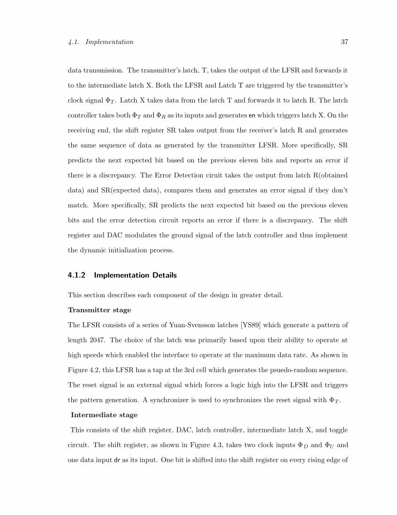
data transmission. The transmitter’s latch, T, takes the output of the LFSR and forwards it
to the intermediate latch X. Both the LFSR and Latch T are triggered by the transmitter’s
clock signal ΦT . Latch X takes data from the latch T and forwards it to latch R. The latch
controller takes both ΦT and ΦR as its inputs and generates en which triggers latch X. On the
receiving end, the shift register SR takes output from the receiver’s latch R and generates
the same sequence of data as generated by the transmitter LFSR. More specifically, SR
predicts the next expected bit based on the previous eleven bits and reports an error if
there is a discrepancy. The Error Detection ciruit takes the output from latch R(obtained
data) and SR(expected data), compares them and generates an error signal if they don’t
match. More specifically, SR predicts the next expected bit based on the previous eleven
bits and the error detection circuit reports an error if there is a discrepancy. The shift
register and DAC modulates the ground signal of the latch controller and thus implement
the dynamic initialization process.
4.1.2 Implementation Details
This section describes each component of the design in greater detail.
Transmitter stage
The LFSR consists of a series of Yuan-Svensson latches [YS89] which generate a pattern of
length 2047. The choice of the latch was primarily based upon their ability to operate at
high speeds which enabled the interface to operate at the maximum data rate. As shown in
Figure 4.2, this LFSR has a tap at the 3rd cell which generates the psuedo-random sequence.
The reset signal is an external signal which forces a logic high into the LFSR and triggers
the pattern generation. A synchronizer is used to synchronizes the reset signal with ΦT .
Intermediate stage
This consists of the shift register, DAC, latch controller, intermediate latch X, and toggle
circuit. The shift register, as shown in Figure 4.3, takes two clock inputs ΦD and ΦU and
one data input dr as its input. One bit is shifted into the shift register on every rising edge of

4.1. Implementation 38
reset
0 31 2 4 11
Figure 4.2: LFSR
dr
PhiD
PhiX
C1 C2 C3 C4C0 GndReset
Figure 4.3: Shift Register
ΦD. Once the shift register has a set of six data values, ΦU goes high generating the output
C0 through C4 and the gndReset signal. With proper sequence of data, this circuit can act as
a shift register. The DAC(Figure 4.4) takes the output from the shift register and generates
a ground signal for the latch controller of the corresponding voltage. This is achieved as
follows: The inverter blobks B0 through B4 are of varying gate width with B0 having the
widest gate width and B4 with the narrowest gate width. This leads to B0 providing the
C0 C1 C2 C3 C4
Block 0 Block 1 Block 2 Block 3 Block 4
resetfalseGroundto Latch Controller
Voltage Follower
Figure 4.4: DAC
4.1. Implementation 39
x
e
z q
Φ
ΦΦ
y
d
Φ
Φ
w
Figure 4.5: Modified Yuan-Svensson Latch
weakest pull-up on the p-channel transistor of voltage follower. Similarly B4 provides the
strongest pull-up. This provides the first 24 step gradient on the signal falseGround which
forms the ground signal for the latch controller. The n-channel transistors which start
conducting only when both C3 and C4 are high, provide the next 8 steps of the gradient.
The reset signal indicates the end of dynamic intialization and thus brings falseGround
completely low and allows the latch controller to run at its higest speed.
Using the DAC circuits, the ground signal of the latch controller can be lowered gradu-
ally. The resetGnd goes high at the end of the sequence which brings the falseGround signal
to its low value. Thus, the latch controller can be initialized at a very slow speed and it
slowly speeds up following the gradient of the ground signal.
The Yuan-Svensson latch, due to its sensitivity towards high data input when the clock
input is high, has a rather large set-up time requirement for a low data input and thus
is not suitable for the latches T,X and R of the design. The modified latch as shown in
Figure 4.5, avoids the problem by attaching the data input to the pull-down path of the
output of both p-stage and n-stage of the latch. Thus, while the clock input is high, if the
data goes low and then high, the output of the latch remains stable thus reducing the large
setup time requirement for low data inputs.
The set-up and hold times for our latches were found to be roughly 150ps and 90ps
respectively from the simulation studies. These times are much shorter than the delays

4.1. Implementation 40
c
cB enB enBB enBBBen
To Latch X
Figure 4.6: en generation
40 31 2 65 11
Ideal recvIP
Figure 4.7: Receiver Shift Register
though the latch control circuitry. I widen the skew tolerance window by delaying the
clocks for latches latch-T and latch-R(δ1 and δ2). With this padding, the skew tolerance of
the interface is determined by the minimum cycle time of the latch controller. This cycle
time is 340ps. Thus, the skew tolerance window has width, 2P −680ps. The skew window is
wider than the clock period for a clock period of 1400MHz or lower. Under these conditions,
the interface can operate with an arbitrary fixed skew. Initially, the self-resetting latch con-
troller generated pulses on en that were of marginal width for triggering the latches. I did
not want to modify the latch controller as this would increase its cycle time and decrease its
skew tolerance. Instead, I used a self-resetting buffer to generate en as shown in Figure 4.6
and widened the pulse by including sufficient delay, in the reset path for the buffer. This
buffer takes c output from the latch controller(see Figure 3.6)and generates the en signal
which triggers the latch X. Finally the toggle circuit converts the narrow pulse on en into
one transition per pulse to facilitate off-chip observation.
Receiver stage
The receiver stage consists of receiver’s latch R, shift register SR and an error detection

4.2. Test Results 41
RSYS0 YS1 YS2 YS3
YS4YS5YS6
recvIP
Ideal s
rb
Error
Figure 4.8: Error Detection Circuit
circuit. The shift register SR, takes output from the latch recvIP as its input and recreates
an ideal pattern of data which is sent as input to the error circuit. The error detection
circuit consists of a series of Yuan-Svensson latches along with an RS latch. As seen in
Figure 4.8, the XOR gate generates a high signal whenever the obtained data differs from
the expected data. The rest of the latches keep the error signal high for one out of six
receiver clock cycles. Thus, an error propagating through the receiver shift register does
not produce multiple error reports.
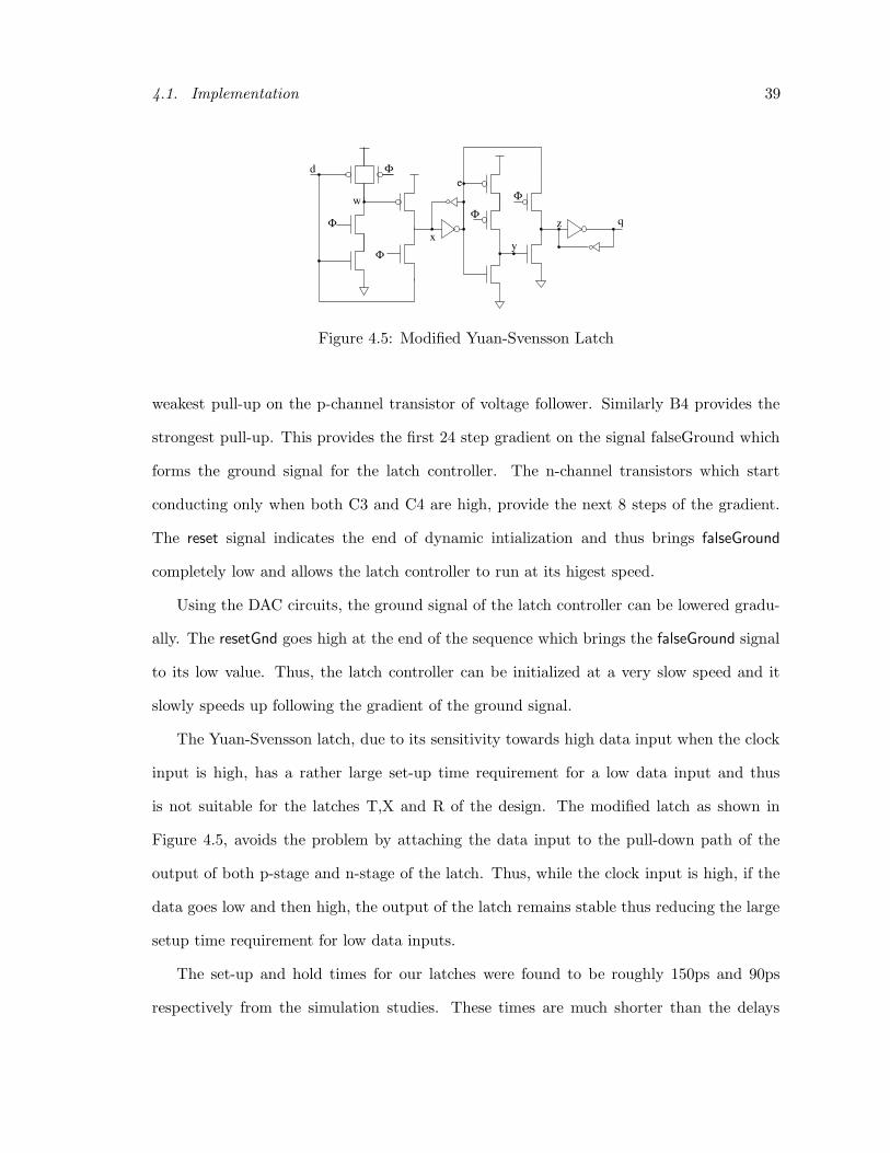
4.2 Test Results
Figure 4.9 shows the structure of the chip.
It has a set of six input signals as follows:
1. ΦT : transmitter’s clock
2. ΦR: receiver’s clock
3. reset: resets the LFSR of the transmitter’s domain
4. ΦU , ΦD and dr: input to the ground modulator of the latch controller.
and four output signals are:
1. transOP: output data of the transmitter’s domain
2. recvIP: input data to the receiver’s domain
3. enToggle: Toggled version of the signal en
4. error: shows error when data from the two domains do not agree.
4.2. Test Results 42
ΦT ΦR
ΦU
ΦDreset
dr
Agilent 81200enToggle
Core Design
transOP
errorrecvIP
signal generatorsynthesized
Agilent 8373B
SRS DS345synthesized fn generator
Parallel BERT
Rhode&SchwarzSMT03signal generator
Figure 4.9: Test Setup

4.2. Test Results 43
I tested the chip in the System-on-Chip Lab of UBC. The signal ΦT was generated from
a Rhode&Schwarz SMT03 Signal Generator with phase modulation ability. The output
ΦR, generated from Agilent 8373B, also formed external clock reference for Agilent 81200.
To achieve complete synchronization between ΦT and ΦR, a synthesized function generator
provided a common time base. The parallel BERT, Agilent 81200, generated the other
programmed input signals, namely, reset, ΦD, ΦU and dr.
With the reset signal going high, I observed the correct psuedo-random sequence on
transOP using an oscilloscope. As soon as the intialization process was completed using
ΦD, ΦU and dr, the recvIP signal exhibitted the same pattern at a fixed offset to transOP.
This verified the functioning of the latch controller. To verify the functionality of LFSR, I
programmed the Agilent 81200 to generate a pulse with a period of 2047 units, to match the
pattern length of the LFSR, and used this pulse to trigger the oscilloscope. Then, stable
data patterns were observed on transOP and recvIP. Due to a top-level wiring error, the
output of the signal Error was shorted and thus I devised additional methods of detecting
errors as explained later.
To measure the skew tolerance of the design, I phase modulated the transmitter grad-
ually until the interface no longer operated successfully as indicated by our error detection
methods described later. The observed error free zone is based on the following principle: at
any arbitrary phase offset between the ΦT and ΦR, the interface can handle a skew tolerance
of almost two clock periods; but the amount of skew tolerance in either direction, meaning
with transmitter earlier or later than the receiver, is non-uniform. As an example, fig 4.10
shows two scenarios with different displacement of the skew tolerance windows. In the first
scenario, ΦT and ΦR are exactly matched in phase and thus ΦT can happen a clock period
earlier or later than the receiver. Thus, an error free zone of almost two clock periods can
be observed in this case. In the second scenario, ΦT and ΦR are 180 degrees out of phase.
In this case, ΦT can happen half a clock period later and one and half clock periods earlier
than the receiver. Because ΦT moves equally in either direction during phase modulation,

4.2. Test Results 44
PhiT
PhiR
en
Error Free Zone
PhiT
PhiR
en
Error Free Zone
Figure 4.10: Skew Tolerance Window

4.2. Test Results 45
0 50 100 150 200 250 300 3503
3.5
4
4.5
5
5.5
6
6.5
initial phase offset(degrees)
phas
e m
odul
atio
n to
lera
nce
(rad
ians
)
peak at(168,6.2)
phase modulation tolerance vs. intial phase offset
Figure 4.11: Phase Modulation Tolerance at 20MHz
I observed errors as soon as it hit the closer boundary. Thus, a phase modulation of more
than half clock period resulted in errors. Any phase offset intermediate of these two val-
ues resulted in an error free zone of some intermediate displacement. Thus, the ideal plot
would depict a minimum error free zone at zero phase offset between ΦT and ΦR and would
gradually increase with the increase in phase difference as it reaches 180 degrees. Further
increase in phase offset would result in gradual decrease in error free zone until it reaches
the minimum again.
I started with ΦT and ΦR operating at about 20MHz. The plot obtained is shown in
Figure 4.11. As expected, the phase modulation tolerance first increased and then decreased
with increasing initial phase offset between transmitter and receiver. The maximum phase
modulation obtained, which is about 6.2 radians suggested a skew tolerance of almost 2
clock periods and implies a cycle time for the latch controller of 662 picoseconds. Similarly,
at 30MHz, as shown in Figure 4.12 a maximum phase tolerance of 6.17 radians is obtained
which is once again almost two clock periods.
To detect the boundaries of the error free zone, and thus determine the skew tolerance
of the design, I devised two methods:

4.2. Test Results 46
0 50 100 150 200 250 300 3503
3.5
4
4.5
5
5.5
6
6.5
initial phase offset(degrees)
phas
e m
odul
atio
n to
lera
nce
(rad
ians
)
peak at(157,6.17)
phase modulation tolerance vs. intial phase offset
Figure 4.12: Phase Modulation Tolerance at 30MHz
• Method 1: In this method, the transmitter and receiver are initialized at some
phase offset from each other. The outputs transOP and recvIP are observed on an
oscilloscope. The transmitter is then phase modulated with the amount of phase
modulation increased gradually. Initally the output from recvIP is stable and does
not drift with time. This is possible due to operation of the latch controller in the
receiver-last mode. But when the amount of phase modulation is such that it hits one
of the boundaries of the error-free zone, the recvIP output drifts by a clock period at
every cycle due to shifts in the mode of operation from receiver-last to transmitter-last
as the controller crossed the boundaries of feasible window of operation.
• Method 2: In this method, the Agilent 81200 was controlled programmatically. The
output recvIP was captured and observed. A lookup table was constructed internally
consisting of identical pattern of data as produced by the transmitter LFSR. The first
11 bits of any block of captured data, indicated its position in the lookup table and
then the subsequent bits were compared against the lookup table and any inconsis-
tency were reported as “error”. Once again the transmitter was phase modulated
with the amount of phase modulation gradually increased. The output of recvIP was

4.2. Test Results 47
attached to Agilent 81200 and when the amount of phase modulation crossed the
feasible range, “errors” were reported by the software which determined the position
of the error free zone.
This chapter desrcibed the implementation details of a proof-of-concept chip demon-
strating the functionality of minSTARI. The test data is generated and verified on the chip
itself using additional structures. Subsequent sections describe the test setup and the vari-
ous observations and results obtained from testing the silicon. The design has been shown
to be possesing very high skew tolerance at lower frequencies. I am in the process of further
testing the interface at higher frequencies ranging up to 2 GHz. Once the skew tolerance
limits are confirmed are higher frequencies, the robustness of the interface will be tested
using dynamic initialization.

Chapter 5
Generalizations: Rational, Close and
Arbitrary Clocks
This chapter describes extensions of our basic interface, which can handle multipe clock do-
main designs with rational, nearly matched and arbitrary, stable clocks. As the frequencies
of the clocks of different domains can differ, data is not transmitted or received at every
cycle of the faster clock. Thus, proper flow control is necessary to ensure reliable commu-
nication between domains. I start with the scenario where clock frequencies are rational
multiples of each other. Sections 5.2 and 5.3 extend the design further to scenarios where
clocks are nearly matched in frquency or have arbitrary and stable frequencies.
5.1 Rational Clock Frequency Multiples
Consider the situation depicted in Figure 1.2: the frequencies of the sender’s and receiver’s
clocks are pre-determined rational multiples of each other. Let PT be the period of the
transmitter’s clock and PR be the period of the receiver’s clock. Let NR and NT be positive
and mutually prime with NR/NT = PT /PR (NT and NR correspond to the frequencies
of the respective clocks). I developed my designs assuming NR > NT and describe the
NT > NR case at the end of this section.
48

5.1. Rational Clock Frequency Multiples 49
latch−X
ΦT ΦR
ΦU
latch controller
QD
tran
smitt
erfr
om
ntnr
data
valid_next
data
to re
ciev
er
multiplierrate
Figure 5.1: An Interface with Rational Clocks
Figure 5.1 shows the design for NR > NT . By the assumption that the receiver operates
at a higher rate than the transmitter, there will be receiver cycles for which no new trans-
mitted data is available. The rate multiplier outputs NT pulses on node ΦU to the latch
controller for every NR cycles of the receiver’s clock as shown below:
sum := 0;
for each cycle of ΦR do
if sum ≥ 0 then
output a pulse on ΦU ;
sum := sum + NT − NR;
else sum := sum + NT ;
endif
od
By analogy with ΦR and Φ′
R, let ΦU ′ be the internally delayed version of ΦU in the latch
controller, and let δT ′U ′ and δU ′T ′ be defined as δT ′R′ and δR′T ′ , respectively. As noted above,
the rate multiplier introduces periodic jitter into ΦU with a period of NRPR = NT PT . Let
δU ′T ′,0 denote the time from the rising edge of ΦU ′ produced by the (kNR)th rising edge of
ΦR to the next rising edge of ΦT ′ for any integer k. It is straightforward to show:
min(δU ′T ′) = δU ′T ′,0
max(δU ′T ′) = δU ′T ′,0 + PR − PR
NT
min(δT ′U ′) = PT − δU ′T ′,0 − PR + PR
NT
max(δT ′U ′) = PT − δU ′T ′,0
(5.1)

5.1. Rational Clock Frequency Multiples 50
ΦT
ΦR
ΦU,1
ΦU,2
−2 −1 2 0 −21
21 −1
sum1
sum2 2
10
0 −2 0 −2
BA
C
Figure 5.2: Exploiting Periodic jitter
The cycle time constraints of the latch controller can be satisfied if:
max(δU ′T ′,0, PT − δU ′T ′,0 − PR + PR
NT) > η (5.2)
which holds for any value of δU ′T ′,0 if:
PT − (1 − 1
NT)PR > 2η (5.3)
For designs where the latch set-up and hold requirements are the dominant constraints, sim-
ilar bounds for PT and PR can be derived. Thus, the one-stage FIFO can interface between
synchronous domains operating at different, rationally related frequencies. Furthermore,
the initialization methods described in Section 3.3.1 apply directly to the rational clocks
case. Comparing equation 5.3 with equation 3.2 shows that the minimum period required
for the slower clock has been increased by the jitter of ΦU created by the rate multiplier.
The rate multiplier introduces periodic jitter. We can exploit this predictability to
increase the robustness of the interface. For every NR consecutive cycles of the receiver’s
clock, the variable sum takes on each value in {NT − NR, . . . , NT − 1} exactly once. The
initial value of sum is arbitrary, and we can use this freedom to increase the skew tolerance
of our design.

5.1. Rational Clock Frequency Multiples 51
Figure 5.2 shows the operation of our interface where the transmitter clock frequency
is 3/5 that of the receiver. The traces for sum1 and ΦU,1 show the worst-case sequence for
sum: with this choice η < PR/2 must hold for proper operation. In particular, if the ΦU
event generated when sum1 transitions from 2 to 0 triggers the latch controller to produce
a ΦX event, then the self-reset cycle must complete in time for the rising edge of ΦT that
occurs PR/2 later (indicated by the arrow labelled A in the diagram). On the other hand,
if this ΦU event does not trigger the latch controller, then the subsequent ΦT event must,
and the resulting self-reset cycle must complete in time for the next ΦU event, again PR/2
later (indicated by the arrow labelled B in the diagram).
The traces for sum2 and ΦU,2 show the optimal sequence for sum for the same transmitter
and receiver clocks. For this scenario, the critical timing occurs when the rising edge of
ΦU that is produced when sum2 goes from 2 to 0 triggers a ΦX pulse. The self-reset of
the latch controller must complete prior to the next ΦU pulse PR time units later. Thus,
with this choice of the sum sequence, the latch controller can operate at half the rate as
required by the worst-case sequence. I first derive the constraints on PT and PR that ensure
proper operation for any phase difference between the two clocks assuming the optimal sum
sequence. I then describe how our initialization technique from Section 3.3.1 can be adapted
to find this sequence.
Regardless of how the sum sequence is chosen, the ΦU clock has a jitter of (1−1/NT )PR
with respect to an evenly spaced clock with period PT . The maximally robust sequence for
sum centers the ΦU jitter interval as closely as possible on the ΦT clock. The interval may
be off center by as much as gcd(PR, PT ) = PR/NT due to the discrete set of choices for the
sum sequence. From these observations, the smaller of the time from a rising edge of ΦT ′
that triggers the latch controller to the next rising edge of ΦU ′ or vice-versa is PT − PR/2.
It is also possible that a rising edge of ΦU ′ triggers the latch controller and that the next
input event for the controller is the next rising edge of ΦU ′ . The minimum time between
two such rising edges is bNR/NT cPT . Combining these two constraints yields that there is
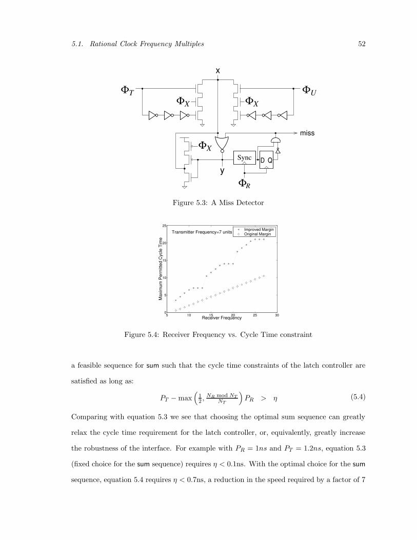
5.1. Rational Clock Frequency Multiples 52
ΦX
ΦX ΦX
ΦU
Φ
ΦT
Q
miss
Sync D
R
y
x
Figure 5.3: A Miss Detector
5 10 15 20 25 300
5
10
15
20
25
Receiver Frequency
Max
imum
Per
mitt
ed C
ycle
Tim
e
Transmitter Frequency=7 units Improved MarginOriginal Margin
Figure 5.4: Receiver Frequency vs. Cycle Time constraint
a feasible sequence for sum such that the cycle time constraints of the latch controller are
satisfied as long as:
PT − max(
1
2, NR mod NT
NT
)
PR > η (5.4)
Comparing with equation 5.3 we see that choosing the optimal sum sequence can greatly
relax the cycle time requirement for the latch controller, or, equivalently, greatly increase
the robustness of the interface. For example with PR = 1ns and PT = 1.2ns, equation 5.3
(fixed choice for the sum sequence) requires η < 0.1ns. With the optimal choice for the sum
sequence, equation 5.4 requires η < 0.7ns, a reduction in the speed required by a factor of 7

5.1. Rational Clock Frequency Multiples 53
for this example. As another example, Figure 5.4 shows the improved margin obtained by
choosing the optimal sum sequence with a fixed transmitter frequency which in this case is
7 units.
The sequence for sum that maximizes robustness can be selected as part of the initial-
ization of the interface. This approach is based on two observations. First, the optimal
sequence works with a larger value of η than any other sequence. Second, we can shift from
one sequence to another by adding NT +1 (resp. NT −NR +1) to sum instead of NT (resp.
NT −NR). Generalizing the initialization technique described in Section 3.3.1, we can start
with a large value for η and gradually decrease it. Each time the latch-controller fails to
reset in time for the next ΦT ′ or ΦU ′ event, we shift to the next sum sequence. When η
is small enough that the latch controller can operate with the optimal sum sequence, but
not the others, then the rate multiplier will switch from one sequence to the next until it
reaches the optimal one. At this point, the latch controller will successfully reset after each
cycle in time for the next ΦT ′ and ΦU ′ events, and the rate multiplier will remain with the
optimal sequence.
Figure 5.3 shows my circuit that reports when a rising edge of ΦT or ΦX arrives at the
latch controller prior to the completion of the controller’s internal reset. Such an event is
called a “miss” and I call the circuit a “miss detector”. A miss occurs if a rising edge is
received while the c signal of the latch controller (see Figure 3.6) is still low. Noting that
ΦX is an inverted version of c, we can use the ΦX signal in the series stacks of transistors
that detect such events. The delay of the inverter that produces ΦX gives our circuit a
little extra margin: it also reports “near misses”. When a (near) miss occurs, node x goes
low and node y goes high. These transitions occur asynchronously with respect to ΦR. It
is assumed that the pulse width of ΦX is less than ΦR to ensure that the “miss” signal is
asserted for only one period of ΦR. The synchronizer provides a delayed version of y in the
receiver’s clock domain and the receiver switches to the “next” sequence on the reported
“miss”. The synchronizer is only active during initialization and does not contribute to the

5.2. Plesiochronous Interfaces 54
missT
D QD Q
ΦT
D Q
detector‘‘near’’ miss
ΦRController−stuff +stuffLatch
missR
Figure 5.5: Interface for Nearly Matched Clocks
latency of data transfers under steady-state operation. Accordingly, the synchronizer can
have a large latency and correspondingly minuscule probability of failure.
This section has shown how minSTARI can be extended for use in designs with multiple,
rationally related clock frequencies. I have focused on the case where the receiver clock
frequency is greater than that of the transmitter. If the transmitter has the higher clock
frequency, equivalent designs can be used with the rate multiplier in the transmitter’s clock
domain.
5.2 Plesiochronous Interfaces
Now consider designs with multiple clock domains with independent clocks that are closely
matched in frequency; these are called “plesiochronous” interfaces (see [Mes90, DDX95]).
Such designs occur, for example, when the sender and receiver are physically separated (e.g.
networks), or when separate clock generators are used to avoid introducing a single point
of failure into the design. Typically, the clock frequencies will be matched to within a few
parts per million, a tolerance that is easily achieved with crystal oscillators.
With close frequency matching, the relative timing of clock edges at the latch interface
changes very slowly. In particular, critical synchronization events occur at a rate corre-
sponding to the difference between the clock frequencies. We can modify the miss detector
circuit from Figure 5.3 to provide an output indicating when a rising edge from ΦT occurs

5.2. Plesiochronous Interfaces 55
shortly after the latch controller completes its reset, and another output indicating when
the timing of ΦR is close to the margin. Furthermore, we can use a delayed version of ΦX
so that near-misses will be reported when a significant margin still remains. If these signals
indicate, for example, when only 0.1P of margin remains, thousands of cycles remain before
an error could actually occur. Thus, we can synchronize these signals to the transmitter
and receiver clocks with extremely high reliability, and use the synchronized versions to take
appropriate corrective action. For example, if a rising edge of ΦR occurs less than 0.1P after
the latch controller completes its reset, then the receiver can skip clocking the latch con-
troller on a subsequent cycle. This will switch the interface from operating with the rising
edge of the transmitter’s clock arriving much after the corresponding edge of the receiver’s
clock to operation where the receiver’s clock edge arrives slightly after the transmitter’s.
Likewise, if a rising edge of ΦT occurs less than 0.1P after the latch controller completes
its reset, then the transmitter can skip sending data and clock on a subsequent cycle. Such
protocols are commonly implemented using “stuff bytes” [DDX95] where extra bytes are
padded at the end of a data packet, with padding added if the transmitter lags behind or
deleted if the receiver is slow. Such protocols are easily implemented in the framework of
our latch controller and miss detector.
Although synchronizations are required during operation, the latency of these synchro-
nizations is not critical for the latency of the data path. The data latency for our interface
is always less than 2P . By adding an arbiter to detect when the latch controller is in
receiver-last mode with enough margin to be able to safely switch to transmitter last, the
worst-case data latency can be reduced to slightly greater than P with an average latency
slightly greater than P/2.

5.3. Arbitrary Clock Frequencies 56
D QD Q D Q
detector‘‘near’’ miss
ΦTrate
multiplierrate
multiplier
saturatingcounter
saturatingcounter
Controller−stuff +stuffLatch ΦR
Figure 5.6: Interface for Arbitrary Clocks
5.3 Arbitrary Clock Frequencies
We now consider the case where the transmitter and receiver operate with independent
clocks at arbitrary frequencies. Initially, it might seem that such a design requires the
overhead of synchronizing buffers as described in Section 2.3.2. However, clock frequencies
are extremely stable in nearly all synchronous designs. We can exploit this stability even
if the frequencies aren’t known in advance. We combine our designs from the previous two
sections to support communication with arbitrary clock frequencies.
Firstly, the transmitter and receiver forward their clocks to each other. Each uses a
counter to produce an initial estimate of the clock frequency of the other. These estimates
provide a rational approximation of the ratio of two clock frequencies. If the nominal clock
frequencies are known in advance, this step can be skipped.
Secondly, if the receiver’s clock frequency is higher than that of the transmitter, it
uses a rate-multiplier to create an approximation of the transmitter’s clock. Likewise, the
transmitter uses a rate multiplier if it has the higher clock frequency. The latch controller
operates with the (possibly rate-multiplied) clocks provided by the transmitter and receiver.
Because the frequency values that we have for the two clocks are only approximations,
albeit very accurate ones, the FIFO will be prone to occasional underflow or overflow.
Separate “near-miss” signals for ΦT and ΦR forward near miss events to the client with the

5.4. A FIFO Interface 57
faster clock, i.e. the one using the rate-multiplier. This client updates its estimate of the
other client’s clock frequency thus changing the rate of events output by its rate multiplier.
This is a second-order control system, and a little bit of care is needed to ensure stability.
A simple approach is that the client with the faster clock uses a counter to measure the
time between near miss events and uses this information to update its estimate of the other
client’s clock frequency. This process is quadratically convergent and stable. At the same
time as updating the frequency estimate, a first-order correction can be applied by adding
an offset to sum to bring the latch controller back to a point near the center of its safe
operating region. If the near miss was for the clock generated by the rate multiplier, then
this offset should be negative (to retard the rate multiplier), otherwise it should be positive.
As for the plesiochronous interface described in the previous section, synchronizations
are required during operation. Again, the latency of these synchronizations is not critical for
the latency of the data path. These synchronizations are infrequent; their rate is determined
by the resolution of the rate-multiplier and the drift rate of the clock frequencies.
5.4 A FIFO Interface
The interfaces presented in the Sections 5.1 through 5.3 do not provide data transfers on
every cycle of the transmitter and receiver clocks. The cycles on which transfers occur is
determined by the interface. In many designs, the sender and receiver need more control
of when transfers occur. Having solved the problems of mismatched clocks, flow control is
straightforward. For example, Figure 5.7 shows an implementation that presents a FIFO
interface to both the transmitter and receiver. The equations for Empty, gr, and pr are:
Empty = er ∧ ¬pt
gr = Get ∧ ¬er
pr = pt ∧ ¬(er ∧ Get)
(5.5)

5.4. A FIFO Interface 58
d_inputnear_full
d_outget
empty
rate mult.
a1
a0 s
y
rate mult.
ΦTΦR
φRφT
R’φφT’
pt
pr grer
FIFO−R
FIFO−1q’d’Put
D_in
Full
mux
D_out
Get
Empty
d qen
dq
Figure 5.7: Implementing a FIFO interface
FIFO-R is a purely synchronous FIFO clocked by ΦR. FIFO-1 is our single-stage FIFO
design. The two rate-multipliers compensate for frequency differences between ΦR and ΦT ,
and the box labelled “sync” is a synchronizer.
When the transmitter performs a put, it must assert Put and the data at D in until
the next ΦT ′ event. If the transmitter’s clock frequency is no greater than the receiver’s,
then there can be a φT ′ event for every event of ΦT and the interface can accept data from
the transmitter on every cycle. If the transmitter does not perform a Put for some φT ′
event, then the resulting “empty” value will be noted by a false value of pt at the output
of FIFO-1.
If FIFO-R is non-empty, Get requests from the receiver are forwarded to FIFO-R on
gr and data from FIFO-R is output on D out. If FIFO-R is empty, then the receiver is
signalled that data is available if an only if the transmitter performed a Put for the last
transfer of FIFO-1: i.e., pt is true. In this case, the value at the output of FIFO-1 bypasses
FIFO-R and goes directly through the multiplexer to D out. The only increase in latency
for our design is the latency of this multiplexer.
If many cycles elapse without the receiver performing a Get, then FIFO-R may become
full. The near full output of this FIFO indicates that FIFO-R has little remaining capacity.
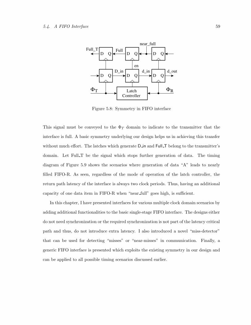
5.4. A FIFO Interface 59
QD QD QD
QDQDQD
D_in d_outd_in
FullFull_Tnear_full
en
ΦΦT RController
Latch
Figure 5.8: Symmetry in FIFO interface
This signal must be conveyed to the ΦT domain to indicate to the transmitter that the
interface is full. A basic symmetry underlying our design helps us in achieving this transfer
without much effort. The latches which generate D in and Full T belong to the transmitter’s
domain. Let Full T be the signal which stops further generation of data. The timing
diagram of Figure 5.9 shows the scenarios where generation of data “A” leads to nearly
filled FIFO-R. As seen, regardless of the mode of operation of the latch controller, the
return path latency of the interface is always two clock periods. Thus, having an additional
capacity of one data item in FIFO-R when “near full” goes high, is sufficient.
In this chapter, I have presented interfaces for various multiple clock domain scenarios by
adding additional functionalities to the basic single-stage FIFO interface. The designs either
do not need synchronization or the required synchronization is not part of the latency critical
path and thus, do not introduce extra latency. I also introduced a novel “miss-detector”
that can be used for detecting “misses” or “near-misses” in communication. Finally, a
generic FIFO interface is presented which exploits the existing symmetry in our design and
can be applied to all possible timing scenarios discussed earlier.

5.4. A FIFO Interface 60
BA
BA
Full_T
Full
d_out
near_full
d_in
D_in
b. receiver−last scenario
Full_T
Full
d_out
near_full
d_in
D_in
a. transmitter−last scenario
BA
A0
BA
BA
Figure 5.9: Timing scenarios with nearly full FIFO-R

Chapter 6
Conclusion
I have presented a very simple design for source-synchronous communication. It is based on
a self-timed, ripple FIFO with a single stage. Whereas a single-stage, pointer FIFO provides
no skew compensation (such a pointer FIFO is simply a latch clocked by the transmitter),
the single-stage ripple FIFO provides nearly two clock periods of skew tolerance and can
operate correctly for any initial phase offset between the transmitter and the receiver of the
channel. The simplicity of the single-stage FIFO enables simplifications and optimization,
thus taking good advantage of self-timed design. I presented a design consisting of a self-
resetting, edge-triggered C-element that generates a clock intermediate to the clocks of the
transmitter and receiver. This intermediate clock strobes a latch that conveys data from
the transmitter to the receiver. The timing of this clock signal ensures that the set-up and
hold requirements of the receiver and the intermediate latch are all satisfied. My design can
be initialized to provide maximal robustness against clock jitter and skew drift by adjusting
the speed of the self-resetting C-element during its initial operation. Alternatively, the
interface can be initialized for minimum latency by deliberately suppressing a transmitter
clock event to the latch during initialization.
Chapter 5 showed how this design can be adapted for more generalized clocking scenarios
including clocks with rationally related frequencies, closely matched clocks, and arbitrary
61

62
clocks. In all of these designs, any synchronization is carried out on a path whose latency
does not impact the data path. Thus, my designs can achieve latencies that are at most
slightly more than one clock period and typically about half the clock period. To achieve
this performance, we exploit the frequency stability of clocks in synchronous designs.
In general, the overheads of synchronization and handshaking are only needed to address
timing issues that cannot be resolved statically. When the clocks of the transmitter and
receiver are identical in frequency, then only the relative phase needs to be resolved, and
this can be done by a simple handshaking circuit such as the latch controller shown in
Figure 3.6. When the clocks are rationally related, the client with the faster clock can
use a rate multiplier to construct an approximation of the other client’s clock. There are
numerous isomorphic sequences of events that can be generated by the rate multiplier, and
synchronization occurs during initialization to determine the optimal sequence. When the
clocks are closely matched in frequency, only the long-term drift needs to be identified. The
synchronizer that detects this drift can have high latency without impacting the data path
latency. Finally, when arbitrary clock frequencies are used, the frequency stability of these
clocks enables accurate approximation of the frequency ratio. Again, synchronization is
only needed to detect long-term drift, and this does not impact the data path latency.
I designed and fabricated a proof-of-concept chip in the TSMC 0.18µ CMOS process
for my design for clients operating at identical clock frequencies using a single-stage FIFO
interface. Intial test results have demonstrated my claims about skew tolerance of the design
and I am in the process of more extensive testing. I am also currently designing a chip to
demonstrate interfaces based on miss-detectors for rational, closely matched and arbitrary
clock frequency designs and will fabricate it in the near future.

Bibliography
[BB98] Daniel W Bailey and Bradley J Benschneider. Clocking design and analysis
for a 600MHz Alpha microprocessor. IEEE Journal of Solid-State Circuits,
33(11):1627–1633, November 1998.
[BC+99] Kerry Bernstein, Keith M. Carrig, et al. High Speed CMOS Design Styles.
Kluwer, 1999.
[BDM02] Keith A. Bowman, Steven G. Duvall, and James D. Meindl. Impact of die-
to-die and within-die parameter fluctuations on the maximum clock frequency
distribution for gigascale integration. IEEE Journal of Solid-State Circuits,
37(2):183–190, February 2002.
[CC+91] Terry I. Chappell, Barbara A. Chappell, et al. A 2-ns cycle, 3.8-ns access 512-
KB CMOS ECL SRAM with a fully pipelined architecture. IEEE Journal of
Solid-State Circuits, 26(11):1577–1585, November 1991.
[CG02] Ajanta Chakraborty and Mark R. Greenstreet. A minimalist source-
synchronous interface. In Proceedings of the 15th IEEE ASIC/SOC Conference,
pages 443–447, September 2002.
[Cha84] Daniel M. Chapiro. Globally-Asynchronous, Locally-Synchronous Systems. PhD
thesis, Department of Computer Science, Stanford University, October 1984.
Tech. Report STAN-CS-84–1026.
[CM73] T.J. Chaney and C.E. Molnar. Anomalous behavior of synchronizer and arbiter
circuits. IEEE Transactions on Computers, C-22(4):421–422, April 1973.
[CN01] Tiberiu Chelcea and Steven M. Nowick. Robust interfaces for mixed-timing
systems with application to latency-insensitive protocols. In Proceedings of the
38th ACM/IEEE Design Automation Conference, pages 21–26, June 2001.
[CZ02] Atanu Chattopadhyay and Zeljko Zilic. High speed asynchronous structures for
inter-clock domain communication. In Proceedings of the 2002 International
Symposium on Circuits and Systems, pages 517–520, September 2002.
[Dam97] Roger A. Dame. The Alphaserver 4100 low-cost clock distribution system.
Compaq Digital Technical Journal, 8(4):38–47, April 1997.
63
Bibliography 64
[Dav99] Bijan Davari. CMOS technology: Present and future. In Proceedings of 1999
Symposium on VLSI Circuits, pages 5–10. IEEE, June 1999.
[DDX95] Larry R. Dennison, William J. Dally, and Duke Xanthopoulos. Low-latency
plesiochronous data retiming. In Proceedings of the Sixteenth Anniversary Con-
ference on Advanced Research in VLSI, pages 304–315, 1995.
[FEG00] S.F. Furber, D. A. Edwards, and J. D. Garside. AMULET3: a 100 MIPS
asynchronous embedded processor. In Proceedings of the 2000 International
Conference on Computer Design, pages 329–334, September 2000.
[GA+02] Stephen Geissler, David Appenzeller, et al. A low-power RISC microprocessor
using dual PLLs in a 0.13µ SOI technology with copper interconnect and low-k
BEOL dielectric. In Proceedings of the 2002 International Solid-State Circuits
Conference, pages 148–149, February 2002.
[Gre93] Mark R. Greenstreet. STARI: A Technique for High-Bandwidth Communi-
cation. PhD thesis, Department of Computer Science, Princeton University,
January 1993.
[Gre95] Mark R. Greenstreet. Implementing a STARI chip. In Proceedings of the 1995
International Conference on Computer Design, pages 38–43, Austin, Texas,
October 1995.
[HN01] David Harris and Sam Naffziger. Statistical clock skew modeling with data
delay variations. IEEE Transactions on VLSI Systems, 9(1):888–898, December
2001.
[HN03] Shaomei Huang and Radu Negulescu. High-performance mixed-clock commu-
nication with resampling, 2003.
[IM02] Anoop Iyer and Diana Marculescu. Power-performance evaluation of Globally
Asynchronous, Locally Synchronous processors. In Proceedings of the 29th In-
ternational Symposium on Computer Architecture, pages 158–168, June 2002.
[JG93] Howard Johnson and Martin Graham. High-Speed Digital Design: A Handbook
of Black Magic. Prentice Hall, 1993.
[KA+01] Andre Kowalczyk, Victor Adler, et al. The first MAJC microprocessor: A dual
CPU system-on-a-chip. IEEE Journal of Solid-State Circuits, 36(11):1609–
1916, November 2001.
[Kat98] Cameron Katrai. Managing clock distribution and optimizing clock skew in
networking applications. Application Notes #14, Pericom Semiconductor Cor-
poration, 1998.
Bibliography 65
[KB+01] Nasser A. Kurd, Javed S. Barkatullah, et al. Multi-GHz clocking scheme for
Intel r© Pentium r© 4 microprocessor. In Proceedings of the 2001 International
Solid-State Circuits Conference, pages 404–405, February 2001.
[KN+02] Georgios K. Konstadinidis, Kevin Normoyle, et al. Implementation of a third-
generation 1.1-GHz 64-bit microprocessor. IEEE Journal of Solid-State Cir-
cuits, 37(11):1461–1469, November 2002.
[KP+99] Gergios Kornaros, Dionisios Pnevmatikatos, et al. ATLAS 1: Implmenting a
single-chip ATM switch with backpressure. IEEE Micro, 19(1):30–41, Jan/Feb
1999.
[KS96] S Kim and R Sridhar. Self-timed mesochronous interconnection for high-speed
VLSI systems. In Sixth Great Lakes Symposium on VLSI, pages 122–125, March
1996.
[MB+89] Alain J. Martin, Steven M. Burns, et al. The design of an asynchronous mi-
croprocessor. In Proceedings of the Conference on Advanced Research in VLSI,
Caltech, 1989.
[Mes90] David G. Messerschmitt. Synchronization in digital system design. IEEE Jour-
nal on Selected Areas in Communications, 8(8):1404–1419, October 1990.
[MJ+97] Charles E. Molnar, Ian W. Jones, et al. A FIFO ring oscillator performance
experiment. In Proc. International Symposium on Advanced Research in Asyn-
chronous Circuits and Systems, pages 279–289. IEEE Computer Society Press,
April 1997.
[ML+97] Alain J. Martin, Andrew Lines, et al. The design of an asynchronous MIPS
R3000 microprocessor. In Proceedings of the 17th Conference on Advanced
Research in VLSI, pages 164–181, September 1997.
[MS01] Fenghao Mu and Christer Svensson. Self-tested self-synchronization circuit for
mesochronous clocking. In IEEE transactions on Circuits and Systems, pages
129–140, 2001.
[MT+02] S.W. Moore, George Taylor, et al. Point to point GALS interconnect. In
Proceedings of the Eigth International Symposium on Advanced Research in
Asynchronous Circuits and Systems, pages 62–68, April 2002.
[MVF00] Jens Mutterbach, Tomas Villiger, and Wolfgang Fichtner. Practical design of
globally-asynchronous, locally-synchronous sytems. In Proceedings of the Sixth
International Symposium on Advanced Research in Asynchronous Circuits and
Systems, pages 52–59, April 2000.

Bibliography 66
[RB+01] P.A. Riocreux, L.E.M. Brackenbury, et al. A low-power self-timed Viterbi
decoder. In Proceedings of the Seventh International Symposium on Advanced
Research in Asynchronous Circuits and Systems, pages 15–24, 2001.
[RJDC98] Phillip J. Restle, K. A. Jenkins, A Deutsch, and P W Cook. Measurement
and modelling of on-chip transmission line effects in a 400 MHz microprocessor.
IEEE Journal of Solid-State Circuits, 33(4):662–665, April 1998.
[RM+01] Phillip J. Restle, Timothy G. McNamara, et al. A clock distribution network
for microprocessors. IEEE Journal of Solid-State Circuits, 36(5):792–799, May
2001.
[RT00] Stelan Rusu and Simon Tam. Clock generation and distribution for the first
IA-64 microprocessor. In ISSCC00, pages 176–177, 2000.
[RWW+02] Woonghwan Ryu, Albert Lu Chee Wai, Fan Wei, Wai Lai Lai, and Joungho
Kim. Over GHz low-power RF clock distribution for a multiprocessor digital
system. IEEE Transactions on Advanced Packaging, 25(1):18–27, February
2002.
[S03] Ingemar Soderquist. Globally updated mesochronous design style. IJSSC,
38(7):1242–1249, 2003.
[Sei79] Charles L. Seitz. System timing. In Introduction to VLSI Systems (Carver
Mead and Lynn Conway), chapter 7, pages 218–262. Addison Wesley, 1979.
[Sei94] Jakov N. Seizovic. Pipeline synchronization. In Proceedings of the First In-
ternational Symposium on Advanced Research in Asynchronous Circuits and
Systems, pages 87–96. IEEE Computer Society Press, 1994.
[SF01] Ivan Sutherland and Scott Fairbanks. GasP: A minimal FIFO control. In
Proceedings of the Seventh International Symposium on Advanced Research in
Asynchronous Circuits and Systems, pages 46–53, April 2001.
[SH97] S Sidiropoulos and M Horowitz. A semi-digital DLL with unlimited phase
shift capability and 0.08-400 MHz operating range. In Proceedings of the 1997
International Solid-State Circuits Conference, pages 332–333, February 1997.
[SM00] Allen E. Sjogren and Chris J. Myers. Interfacing synchronous and asynchronous
modules within a high-speed pipeline. IEEE Transactions on VLSI Systems,
8(5):573–583, October 2000.
[SPL02] Tiberiu Seceleanu, Juha Piosila, and Pasi Liljeberg. On-chip segmented bus: A
self-timed approach. In Proceedings of the 15th IEEE ASIC/SOC Conference,
pages 216–220, September 2002.
Bibliography 67
[TR+00] Simon Tam, Stefan Rusu, et al. Clock generation and distribution for the first
IA-64 microprocessor. IEEE Journal of Solid-State Circuits, 35(11):1545–1552,
November 2000.
[WGG02] Anthony J. Winstanley, Aurelien Garivier, and Mark R. Greenstreet. An
event spacing experiment. In Proceedings of the Eigth International Sympo-
sium on Advanced Research in Asynchronous Circuits and Systems, pages 42–
51, Manchester, UK, April 2002.
[Wik03] Daniel Wiklund. Mesochronous clocking and communication in on-chip net-
works. In Proceedings of Swedish System-on-chip conference, April 2003.
[XB+01] Thucydides Xanthopoulus, Daniel W Bailey, et al. The design and analysis of
the clock distribution network for a 1.2 GHZ alpha microprocessor. In ISSCC01,
pages 402–403, 2001.
[YD96] Ken Y. Yun and Ryan P. Donohue. Pausible clocking: A first step toward
heterogeneous systems. In Proceedings of the 1996 International Conference on
Computer Design, pages 118–123, October 1996.
[YH00] Evelina Yeung and Mark A. Horowitz. A 2.4 Gb/s/pin simultaneous bidirec-
tional parallel link with per-pin skew compensation. IEEE Journal of Solid-
State Circuits, 35(11):1619–1628, November 2000.
[YS89] Jiren Yuan and Christer Svensson. High-speed CMOS circuit technique. IEEE
Journal of Solid-State Circuits, 24(1):62–70, February 1989.