e guro masters
DESCRIPTION
eurgoTRANSCRIPT
RaPiD-AES: Developing an Encryption-Specific FPGA Architecture
Kenneth Eguro
A thesis submitted in partial fulfillment of the requirements for the degree of
Master of Science in Electrical Engineering
University of Washington
2002
Program Authorized to Offer Degree: Electrical Engineering


University of Washington
Abstract
RaPiD-AES: Developing Encryption-Specific FPGA Architectures
Kenneth Eguro
Chair of the Supervisory Committee: Associate Professor, Scott Hauck
Electrical Engineering
Although conventional FPGAs have become indispensable tools due to their versatility and quick design
cycles, their logical density, operating frequency and power requirements have limited their use. Domain-
specific FPGAs attempt to improve performance over general-purpose reconfigurable devices by
identifying common sets of operations and providing only the necessary flexibility needed for a range of
applications. One typical optimization is the replacement of more universal fine-grain logic elements with
a specialized set of coarse-grain functional units. While this improves computation speed and reduces
routing complexity, this also introduces a unique design problem. It is not clear how to simultaneously
consider all applications in a domain and determine the most appropriate overall number and ratio of
different functional units. In this paper we show how this problem manifests itself during the development
of RaPiD-AES, a coarse-grain, domain-specific FPGA architecture and design compiler intended to
efficiently implement the fifteen candidate algorithms of the Advanced Encryption Standard competition.
While we investigate the functional unit selection problem in an encryption-specific domain, we do not
believe that the causes of the problem are unique to the set of AES candidate algorithms. In order for
domain-specific reconfigurable devices to performance competitively over large domain spaces in the
future, we will need CAD tools that address this issue. In this paper we introduce three algorithms that
attempt to solve the functional unit allocation problem by balancing the hardware needs of the domain
while considering overall performance and area requirements.


i
Table of Contents
Page
List of Figures ..........................................................................................................................................ii 1 Introduction..................................................................................................................................... 1 2 Background..................................................................................................................................... 2
2.1 Encryption.............................................................................................................................. 2 2.2 Field Programmable Gate Arrays ............................................................................................ 3 2.3 Previous FPGA-based Encryption Systems ............................................................................. 4 2.4 RaPiD Architecture ................................................................................................................ 5 2.5 RaPiD-C................................................................................................................................. 6
3 Implications of Domain-Specific Devices......................................................................................... 6 4 Functional Unit Design .................................................................................................................... 8 5 Difficulties of Functional Unit Selection ........................................................................................ 10 6 Function Unit Allocation ............................................................................................................... 12
6.1 Performance-Constrained Algorithm..................................................................................... 12 6.2 Area-Constrained Algorithm................................................................................................. 14 6.3 Improved Area-Constrained Algorithm ................................................................................. 15
7 Function Unit Allocation Results ................................................................................................... 16 8 RaPiD-AES Compiler.................................................................................................................... 22 9 Future Work .................................................................................................................................. 22 10 Conclusions................................................................................................................................... 23 11 Bibliography.................................................................................................................................. 24 Appendix A - Galois Field Multiplication................................................................................................ 27 Appendix B – Hardware Requirements.................................................................................................... 28 Appendix C – Results ............................................................................................................................. 30 Appendix D – RaPiD-AES Components.................................................................................................. 33 Appendix E – Example of RaPiD-AES Implementation: Rijndael............................................................ 39

ii
List of Figures
Page
Figure 1 – Advanced Encryption Standard Competition Timeline.............................................................. 1 Figure 2 – FPGA Implementations of AES Candidate Algorithms............................................................. 5 Figure 3 - Basic RaPiD Cell...................................................................................................................... 6 Figure 4 – Required Operators of the AES Candidate Algorithms.............................................................. 8 Figure 5 – Functional Unit Description ..................................................................................................... 8 Figure 6 – Multi-mode RAM Unit .......................................................................................................... 10 Figure 7 – Ratio Complications............................................................................................................... 11 Figure 8 – Complexity Disparity............................................................................................................. 11 Figure 9 – Scaling Behavior.................................................................................................................... 12 Figure 10 – Performance-Constrained Functional Unit Selection ............................................................. 13 Figure 11 – Area-Constrained Function Unit Selection............................................................................ 15 Figure 12 – Improved Area-Constrained Functional Unit Selection ......................................................... 16 Figure 13 – Minimum Throughput Results of Functional Unit Selection.................................................. 17 Figure 14 – Performance Results Across the Domain of Functional Unit Selection .................................. 18 Figure 15 – Area Results of Functional Unit Selection ............................................................................ 19 Figure 16 – Resource Results from Performance-Constrained Analysis ................................................... 20 Figure 17 – Resource Results from Area-Constrained Analysis ............................................................... 20 Figure 18 – Resource Results from Improved-Area Constrained Analysis................................................ 21 Figure 19 – Component Mixture ............................................................................................................. 21

iii
Acknowledgements
The author would like to thank his advisor, Scott Hauck, for providing both the inspiration for this project
and the opportunity to conduct research under his supportive and insightful guidance.
The author would also like to thank Carl Ebeling and everyone on the RaPiD development team. Their
pioneering work in the exploration of domain-specific reconfigurable devices and high-level language
design compilers made this work possible. The author would like to specifically thank Chris Fisher for his
invaluable assistance dealing with the RaPiD-C compiler.
This research was supported in part by grants from the National Science Foundation.

1
1 Introduction
The Advanced Encryption Standard competition offered a compelling opportunity for designers to exploit
the benefits of domain-specific FPGAs to produce a versatile, fast, and early-to-market encryption device.
Figure 1 provides a brief timeline for the competition. The competition requirements and the candidate
algorithms have several characteristics that make designing specialized, coarse-grain reconfigurable
devices particularly attractive. First, high performance is very important due to today’s large volume of
sensitive electronic traffic. Second, flexibility allows algorithm updates and improvements. In addition,
flexibility was a necessity for pioneering designers since the contest allowed submissions to be modified
during public review to address any security or performance concerns that might be raised. Furthermore,
the control logic and routing structure for the system does not need to be complex since the iterative
dataflow for most of the algorithms conforms to one of three simple styles. Lastly, very few different types
of functional units are needed because all of the required operations can be implemented with a
combination of simple ALUs, multipliers, Galois Field multipliers, bit permutations, memories, and
multiplexors.
January 1997 The National Institute for Standards and Technology issues a public call for symmetric-key block cipher algorithms that are both faster and more secure than the aging Data Encryption Standard.
August 1998 From around the world, twenty-six submissions are received. Fifteen algorithms are accepted to compete in an eight-month review period.
August 1999 Based upon brief but careful public analysis and comment about security and efficiency, five algorithms are selected for further scrutiny.
October 2000 After a nine-month second review period and several public forums, Rijndael is announced as the new encryption standard.
December 2001 The Secretary of Commerce makes the AES a Federal Information Processing Standard. This makes AES support compulsory for all federal government organizations as of May 2002.
Figure 1 – Advanced Encryption Standard Competition Timeline A brief timeline for the Advanced Encryption Standard competition sponsored by the National Institute for Standards and Technology. Based on information from [23]. Note that modifications to four algorithms were submitted between August 1998 and August 1999.
This paper describes the development of the RaPiD-AES system – a coarse-grain, encryption-specific
FPGA architecture and design compiler based upon the RaPiD system [11], also developed at the
University of Washington. We will begin with a short introduction to encryption, FPGAs, and a summary
of previous FPGA-based encryption devices. This will be followed by a brief description of the RaPiD
architecture and the RaPiD-C language. We will move on to a discussion of the development of
encryption-specialized functional units and identify some unique architectural design problems inherent to
coarse-grain, domain-specific reconfigurable devices. We will then introduce three approaches that we
have developed to deal with these problems and describe how this guided the formation of our architecture.
Finally we will describe the modifications that were made to the RaPiD-C compiler so that developers can
map designs to our architecture using a high-level, C-like language.

2
2 Background
The popularity of many online services, such as electronic banking and shopping over the Internet, is only
possible today because we have strong encryption techniques that allow us to control our private data while
it is flowing across public networks. Although the concept of secure communication has only become
familiar to the general public within the last decade, its popularity truly began in the late 1970s. In 1972,
the National Institute of Standards and Technology (then known as the Nation Bureau of Standards)
acknowledged the increasing computer use within the federal government and decided that a strong,
standard cryptographic algorithm was needed to protect the growing volume of electronic data. In 1976,
with the help of the National Security Agency (NSA), they officially adopted a modified version of IBM’s
Lucifer algorithm [31] to protect all non-classified government information and named it the Data
Encryption Standard (DES). While there were some unfounded accusations that the NSA may have
planted a “back-door” that would allow them access to any DES-encrypted information, it was generally
accepted that the algorithm was completely resistant to all but brute-force attacks. While the algorithm
later turned out to be much weaker than originally believed [28], the perceived strength and the official
backing of the US government made DES very popular in the private sector. For example, since all
financial institutions needed the infrastructure to communicate with federal banks, they quickly adopted
DES for use in all banking transactions, from cash machine PIN authentication to inter-bank account
transfers. This not only provided them with more secure communication over their existing private
networks, it also allowed them to use faster, cheaper third-party and public networks.
2.1 Encryption While in the past the security of cryptographic methods relied on the secrecy of the algorithm used to
encrypt the data, this type of cipher is not only inherently insecure but also completely impractical for
public use. Therefore, all modern encryption techniques use publicly known algorithms and rely on
specific strings of data, known as keys, to control access to protected information. There are two classes of
modern encryption algorithms: symmetric, or secret-key, and asymmetric, or public-key. The primary
difference between the two models is that while symmetric algorithms either use a single secret key or two
easily related secret keys for encryption and decryption, asymmetric algorithms use two keys, one publicly
known and another secret.
The AES competition only included symmetric ciphers because they are generally considerably faster for
bulk data transfer and simpler to implement than asymmetric ciphers. However, public-key algorithms are
of great interest for a variety of applications since the security of the algorithm only hinges on the secrecy
of one of the keys. For example, before two parties can begin secure symmetric-key communication they

3
need to agree upon a key over an insecure channel. This initial negotiation can be conducted safely by
using asymmetric encryption. Another reason that public-key algorithms are popular is that by making
small modifications to the way that the algorithms are used, they can often implement a range of
authentication systems. For example, public-key encryption generally uses the public key to encrypt and
the private key to decrypt. While it is not necessarily secure for a party to encrypt a document using its
private key, a receiving party can confirm that the document originated from the sender by decrypting with
the appropriate public key. This can be further extended to provide tamper-resistance, timestamping, and
legally binding digital signatures.
Modern symmetric block ciphers typically iterate multiple times over a small set of core encryption
functions. To make the resulting ciphertext more dependent on the key, each iteration of the encryption
function generally incorporates one or more unique subkeys that are generated from the primary key.
Although some of the AES candidate algorithms allow for on-the-fly subkey generation, many do not. In
order to provide an equal starting point for all of the algorithms, we assume that the subkey generation is
performed beforehand and the subkeys are stored in local memory. For many applications, such as Secure
Shell (SSH), this is a reasonable assumption since a large amount of data is transferred using a single key
once a secure channel is formed. In this case, the startup cost of subkey generation is very minimal
compared to the computation involved in the bulk encryption of transmitted information.
2.2 Field Programmable Gate Arrays As the volume of secure traffic becomes heavier, encryption performed in software quickly limits the
communication bandwidth and offloading the work to a hardware encryption device is the only way to
maintain good performance. Unfortunately, ASIC solutions are not only expensive to design and build,
they also completely lack any of the agility of software implementations. Advances in hardware
technology and cryptanalysis, the science and mathematics of breaking encryption, constantly pursue all
ciphers. This means that very widely employed algorithms may become vulnerable virtually overnight.
While a software-only encryption system would be very slow, it could easily migrate to a different
algorithm, where an ASIC-based encryption device would need to be completely replaced. However, if a
reconfigurable computing device were used instead, it would provide high performance encryption and, if
needed, it is likely that a new cipher could be quickly applied with no additional hardware and negligible
interruption to service.
Field Programmable Gate Arrays, or FPGAs, successfully bridge the gap between the flexibility of
software and performance of hardware by offering a large array of programmable logic blocks that are
embedded in a network of configurable communication wires. The logic blocks, also known as

4
Configurable Logic Blocks (CLBs), typically use small look-up tables, or LUTs, to emulate standard gate
logic. For example, in the Xilinx 4000 series devices [32], each CLB is capable of producing one to two
independent four or five input functions. Each of the CLBs can then be interconnected with others via a
reconfigurable matrix of routing resources. By using RAM to control the routing configuration and the
content of the LUTs, FPGAs can be quickly programmed and reprogrammed to run many different
applications. Furthermore, since the computations are still performed in hardware, FPGA implementations
often outpace software-based solutions by an order of magnitude or more. Unfortunately, FPGA designs
are also generally several times slower, larger and less energy-efficient than their ASIC counterparts. This
has limited their use in applications where flexibility is not essential.
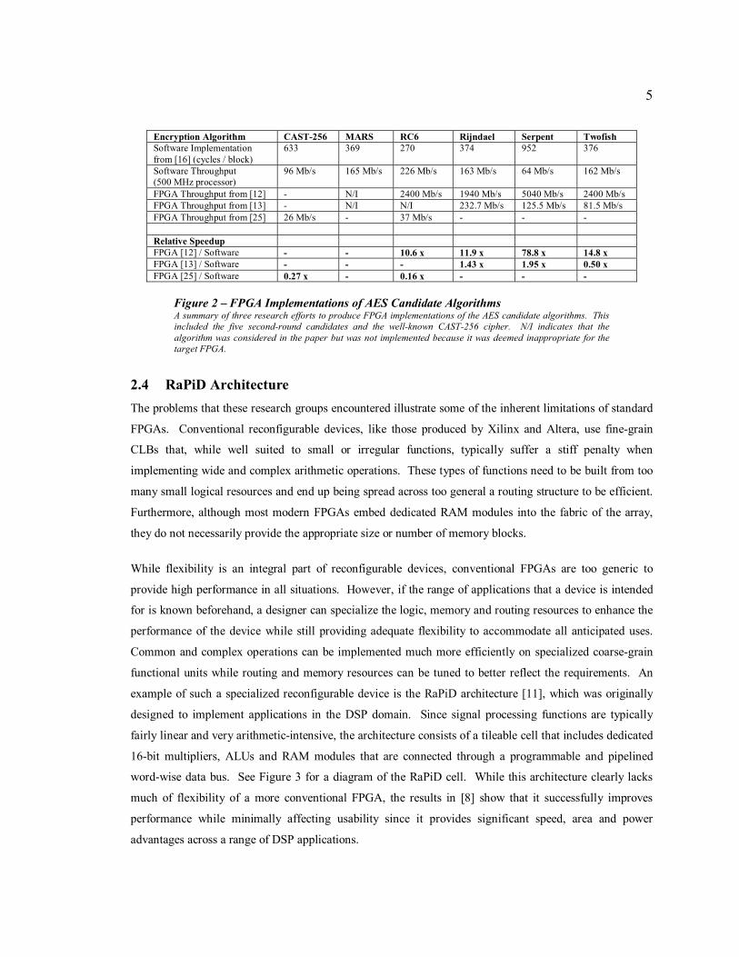
2.3 Previous FPGA-based Encryption Systems FPGAs have been shown to be effective at accelerating a wide variety of applications, from image
processing and DSP to network/communication and data processing. Many research efforts have
capitalized on the inherent flexibility and performance of FPGAs; encryption is no exception. The author
of [18] was among the first to efficiently map DES to a reconfigurable device. This effort attained a
relative speedup of 32x as compared to contemporary software implementations while providing roughly
one-quarter of the performance of ASIC solutions. Later, papers such as [19] and [20] used high-speed
FPGA implementations to prove that DES was vulnerable to brute-force attacks from low-cost, massively
parallel machines built from commodity parts.
When the 15 AES candidate algorithms* were announced in 1998, it sparked new interest in FPGA-based
encryption devices. The authors of [12] showed that four of the five finalist algorithms could be executed
on an FPGA an average of over 21x faster than their best known software counterparts. See Figure 2 for
details of these results. However, this required one of the largest FPGAs available at the time and they
were still unable to implement an efficient version of the fifth algorithm due to a lack of resources on the
device. The authors of [13] and [25] encountered much more serious problems since they attempted to
implement the AES candidate algorithms on much smaller FPGAs. In [13], even though the authors
determined that two of the five finalists were too resource-intensive for their device, the three algorithms
that were implemented still failed to perform well. The average throughput of these implementations was
only about 1.3x that of their software equivalents. Even worse, the mappings from [25] only offered an
average of just over one-fifth the throughput of software-based encryption. These research groups stated
that algorithms were either not implemented or implemented poorly due to memory requirements and
difficult operations such as 32-bit multiplication or variable rotations.
* [1, 2, 4, 5, 9, 10, 14, 15, 17, 21, 22, 24, 26, 27, 30]
5
Encryption Algorithm CAST-256 MARS RC6 Rijndael Serpent Twofish Software Implementation from [16] (cycles / block)
633 369 270 374 952 376
Software Throughput (500 MHz processor)
96 Mb/s 165 Mb/s 226 Mb/s 163 Mb/s 64 Mb/s 162 Mb/s
FPGA Throughput from [12] - N/I 2400 Mb/s 1940 Mb/s 5040 Mb/s 2400 Mb/s FPGA Throughput from [13] - N/I N/I 232.7 Mb/s 125.5 Mb/s 81.5 Mb/s FPGA Throughput from [25] 26 Mb/s - 37 Mb/s - - - Relative Speedup FPGA [12] / Software - - 10.6 x 11.9 x 78.8 x 14.8 x FPGA [13] / Software - - - 1.43 x 1.95 x 0.50 x FPGA [25] / Software 0.27 x - 0.16 x - - -
Figure 2 – FPGA Implementations of AES Candidate Algorithms A summary of three research efforts to produce FPGA implementations of the AES candidate algorithms. This included the five second-round candidates and the well-known CAST-256 cipher. N/I indicates that the algorithm was considered in the paper but was not implemented because it was deemed inappropriate for the target FPGA.
2.4 RaPiD Architecture The problems that these research groups encountered illustrate some of the inherent limitations of standard
FPGAs. Conventional reconfigurable devices, like those produced by Xilinx and Altera, use fine-grain
CLBs that, while well suited to small or irregular functions, typically suffer a stiff penalty when
implementing wide and complex arithmetic operations. These types of functions need to be built from too
many small logical resources and end up being spread across too general a routing structure to be efficient.
Furthermore, although most modern FPGAs embed dedicated RAM modules into the fabric of the array,
they do not necessarily provide the appropriate size or number of memory blocks.
While flexibility is an integral part of reconfigurable devices, conventional FPGAs are too generic to
provide high performance in all situations. However, if the range of applications that a device is intended
for is known beforehand, a designer can specialize the logic, memory and routing resources to enhance the
performance of the device while still providing adequate flexibility to accommodate all anticipated uses.
Common and complex operations can be implemented much more efficiently on specialized coarse-grain
functional units while routing and memory resources can be tuned to better reflect the requirements. An
example of such a specialized reconfigurable device is the RaPiD architecture [11], which was originally
designed to implement applications in the DSP domain. Since signal processing functions are typically
fairly linear and very arithmetic-intensive, the architecture consists of a tileable cell that includes dedicated
16-bit multipliers, ALUs and RAM modules that are connected through a programmable and pipelined
word-wise data bus. See Figure 3 for a diagram of the RaPiD cell. While this architecture clearly lacks
much of flexibility of a more conventional FPGA, the results in [8] show that it successfully improves
performance while minimally affecting usability since it provides significant speed, area and power
advantages across a range of DSP applications.

6
Figure 3 - Basic RaPiD Cell A block diagram of the basic RaPiD cell [6]. The complete architecture is constructed by horizontally tiling this cell as many times as needed. The vertical wires to the left and right of each component represent input multiplexors and output demultiplexors, respectively. The blocks shown on the long horizontal routing tracks indicate bus connectors that both segment the routing and provide pipelining resources.
2.5 RaPiD-C In addition to the hardware advantages of the architecture, the RaPiD researchers show another aspect of
the system that makes it particularly attractive in [7]. This paper describes the specifics of RaPiD-C, a C-
like language that allows developers to map their designs to the RaPiD architecture in a high-level, familiar
way. In addition to the normal C constructs that identify looping, conditional statements, and arithmetic or
logical operations, the language also has specific elements that control off-chip communication, loop
rolling and unrolling, sequential and parallel processing, circuit synchronization, and the pipelining of
signals. These additional constructs make it possible to compile concise hardware descriptions to
implementations that are still faithful to their designer’s original intent.
Furthermore, although the language and compiler were designed for the original RaPiD architecture, the
developers mention in [8] that the system includes enough flexibility to use other special-purpose
functional and memory units. With these extensions, they intended the compiler to be able to map a large
range of computation-intensive applications onto a wide variety of coarse-grain reconfigurable devices.
3 Implications of Domain-Specific Devices
Although domain-specific FPGAs such as RaPiD can offer great advantages over general-purpose
reconfigurable devices, they also present some unique challenges. One issue is that while design choices
that affect the performance and flexibility of classical FPGAs are clearly defined and well understood, the

7
effects that fundamental architecture decisions have on specialized reconfigurable devices are largely
unknown and difficult to quantify. This problem is primarily due to the migration to coarse-grain logic
resources. While the basic logic elements of general-purpose reconfigurable devices are generic and
universally flexible, the limiting portions of many applications are complex functions that are difficult to
efficiently implement using the fine-grain resources provided. As mentioned earlier, these functions
typically consume many flexible, but relatively inefficient, logic blocks and lose performance in overly
flexible communication resources. By mapping these applications onto architectures that include more
sophisticated and specialized coarse-grain functional units, they can be implemented in a smaller area with
better performance. While the device may lose much of its generality, there are often common or related
operations that reoccur across similar applications in a domain. These advantages lead to the integration of
coarse-grain functional elements into specialized reconfigurable devices, as is done in the RaPiD
architecture. However, the migration from a sea of fine-grained logical units to a clearly defined set of
coarse-grained function units introduces a host of unexplored issues. Merely given a domain of
applications, it is not obvious what the best set of functional units would be, much less what routing
architecture would be appropriate, what implications this might have on necessary CAD tools, or how any
of these factors might affect each other.
The first challenge, the selection of functional units, can be subdivided into three steps. First, all
applications in a domain must be analyzed to determine what functions they require. Crucial parts such as
wide multipliers or fast adders should be identified. Next, this preliminary set of functional units can be
distilled to a smaller set by capitalizing on potential overlap or partial reuse of other types of units.
Different sizes of memories, for example, can be combined through the use of multi-mode addressing
schemes. Lastly, based upon design constraints, the exact number of each type of unit in the array should
be determined. For example, if the applications are memory-intensive rather than computationally-
intensive, the relative number of memory units versus ALUs should reflect this.
In Sections 5, 6 and 7 of this paper, we will primarily focus on the problem of determining the most
appropriate quantity and ratio of functional units for our encryption-specialized architecture. While the
Section 4 describes the functional units we included in our system, we did not fully explore the entire
design space. While operator identification and optimization are both complex problems unique to coarse-
grain architectures, we did not address these issues since the algorithms themselves provide an obvious
starting point. Also, since the algorithms use a relatively small number of strongly-typed functional units,
it is fairly simple to perform the logical optimization and technology mapping by hand. Although this may
overlook subtle optimizations, such as the incorporation of more sophisticated operators, this does provide
an acceptable working set.

8
4 Functional Unit Design
Encouraged by the results of the RaPiD project, we decided to build a RaPiD platform specialized for
encryption. While the necessary functional units are different, the RaPiD architecture was designed for
linear, iterative dataflow. However, since it is coarse-grained, there are particular architectural differences
that separate it from general-purpose reconfigurable devices. One major design decision was the bit-width
of the architecture. Since the operations needed by the AES competition algorithms range from single bit
manipulations to wide 128-bit operations, we determined that a 32-bit word size would likely provide a
reasonable compromise between the awkwardness of wide operators and the loss of performance due to
excessive segmenting. In addition, while the algorithms did not preclude the use of 64, 16 or 8-bit
processors, the natural operator width for many of the algorithms was specifically designed to take
advantage of more common 32-bit microprocessors. After defining the bit-width of the architecture, the
next problem was determining a comprehensive set of operators. Analysis identified six primary operation
types required for the AES candidate algorithms. These operation classes lead to the development of seven
distinct types of functional units. See Figure 4 for a list of operation classes and Figure 5 for a description
of the functional unit types implemented in our system.
Class Operations Multiplexor Dynamic dataflow controlRotation Dynamic left rotation, static rotation, static logical left/right shift, dynamic left shift Permutation Static 32-bit permutation, static 64-bit permutation, static 128-bit permutationRAM 4-bit lookup table, 6-bit lookup table, 8-bit lookup tableMultiplication 8-bit Galois Field multiplication, 8-bit integer multiplication, 32–bit integer multiplication ALU Addition, subtraction, XOR, AND, OR, NOT Figure 4 – Required Operators of the AES Candidate Algorithms Table of the six operator classes used in the AES competition algorithms.
Unit Description Multiplexor 32 x 2:1 muxes Rotate/shift Unit 32-bit dynamic/static, left/right, rotate/logical shift/arithmetic shiftPermutation Unit 32 x 32:1 statically controlled muxesRAM 256 byte memory with multi-mode addressing32-bit Multiplier 32–bit integer multiplication (32-bit input, 64-bit output)8-bit Multiplier 4 x 8-bit modulus 256 integer multiplications or 4 x 8-bit Galois Field multiplications ALU Addition, subtraction, XOR, AND, OR, NOT Figure 5 – Functional Unit Description Table of the seven types of functional unit resources in our system.
One peculiarity of a RaPiD-like architecture is the distinct separation between control and datapath logic.
Like the original RaPiD architecture, we needed to explicitly include multiplexors in the datapath to
provide support for dynamic dataflow control. In addition, due to the bus-based routing structure, we
needed to include rotator/shifters and bit-wise crossbars to provide support for static rotations/shifts and bit
9
permutations. Although this seems inefficient since these static operations are essentially free on a general-
purpose FPGA (they are incorporated into the netlist and implemented at compile-time), the AES candidate
algorithms also require dynamic rotations/shifts. These are typically very difficult to implement on
conventional reconfigurable devices. In our architecture, though, the same hardware can be used to provide
support for both static and dynamic rotations/shifts with minimal additional hardware. For future
flexibility, we also decided to add in currently unused operations such as arithmetic shifting. We chose to
implement a dynamically/statically controlled rotation/shift unit separately from a statically controlled
crossbar for two reasons. First, static random bit permutations are needed far less than rotation or shift
operations and we expect the crossbar to be significantly larger than its rotation/shift counterpart. Second,
the additional hardware required to make a crossbar emulate a dynamically controlled rotator/shifter is too
large to be efficient.
Next we considered the logical and arithmetic needs of the algorithms. First, since all of the algorithms
contain addition and subtraction or bit-wise logical operations, we chose to incorporate all of these
functions into one ALU type. For simplicity we decided to extend the 16-bit RaPiD ALU to a 32-bit
version. Second, many of the algorithms require either an 8 or 32-bit integer multiplication or a related
function, an 8-bit Galois Field multiplication. See Appendix A for an explanation of Galois Field
multiplication. Although these operations can be performed using the other functional units that we have
included, the frequency and complex nature of these operations make them ideal candidates for dedicated
functional units. We chose to implement the 32-bit integer multiplier and the 4-way 8-bit integer/Galois
Field multiplier as two separate units for three main reasons. First, the AES algorithms do include
multiplications up to 64 bits. To quickly calculate these multiplications, it was necessary to implement a
wide multiplier. Second, as can be seen from the diagram in Appendix A, it is difficult to make an efficient
multi-mode 32-bit integer/8-bit Galois Field multiplier. Most likely, this unit would only be able to handle
one or possibly two Galois multiplications at a time. This is not efficient in terms of resource utilization or
speed. Lastly, a four-way 8-bit Galois Field multiplier is also able to handle four 8-bit integer
multiplications with minimal modification and little additional hardware.
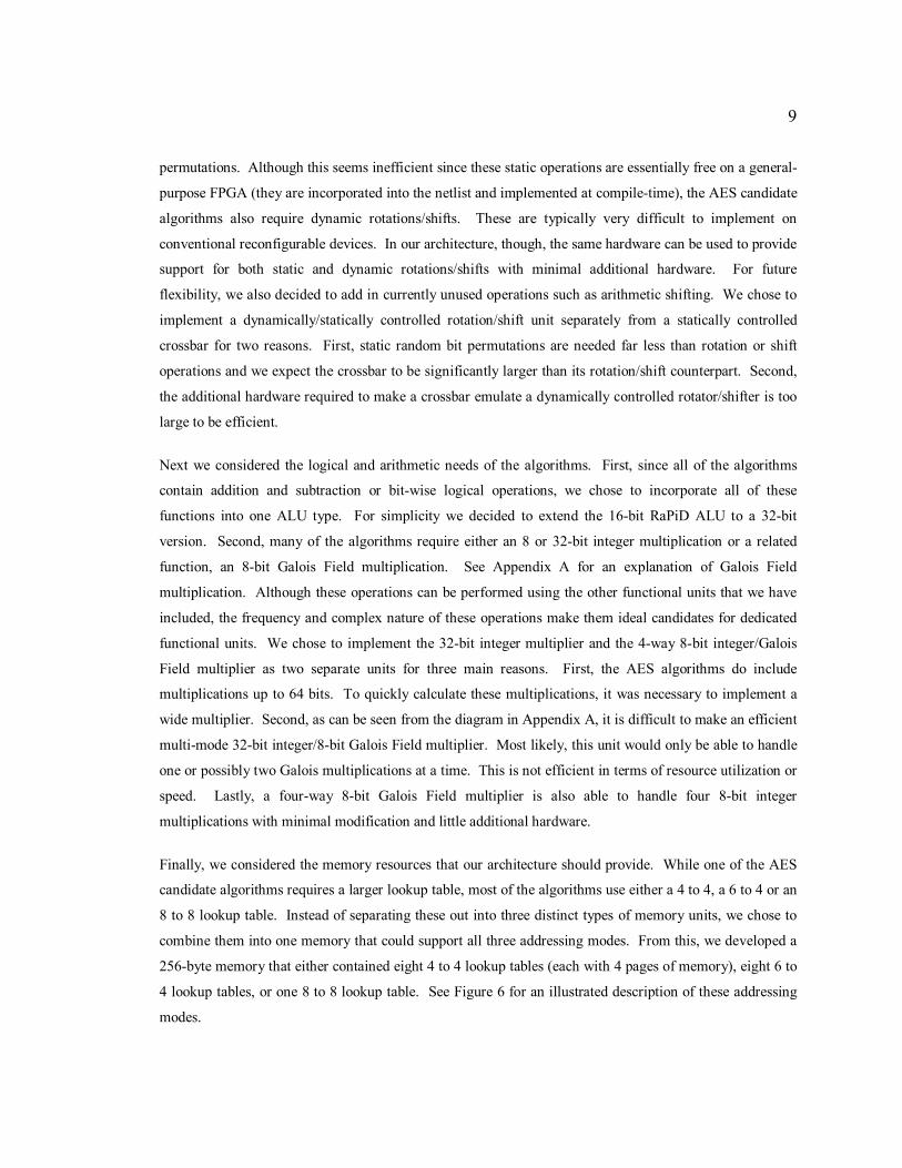
Finally, we considered the memory resources that our architecture should provide. While one of the AES
candidate algorithms requires a larger lookup table, most of the algorithms use either a 4 to 4, a 6 to 4 or an
8 to 8 lookup table. Instead of separating these out into three distinct types of memory units, we chose to
combine them into one memory that could support all three addressing modes. From this, we developed a
256-byte memory that either contained eight 4 to 4 lookup tables (each with 4 pages of memory), eight 6 to
4 lookup tables, or one 8 to 8 lookup table. See Figure 6 for an illustrated description of these addressing
modes.

10
64 nibbles64 nibbles
8 x 4:1 Muxes
8
8 Address Lines
8 Output Lines
64 nibbles64 nibbles
64 nibbles64 nibbles
64 nibbles64 nibbles
6
2
8 8 8
8
8 to 8 Lookup Mode
64 nibbles
64 nibbles
4
48 Address Lines
32 Output Lines
64 nibbles
64 nibbles
64 nibbles
64 nibbles
64 nibbles
64 nibbles
4 4 4 4 4 4 4
6 6 6 6 6 6 6 6
6 to 4 Lookup Mode
64 nibbles
64 nibbles
4
32 Address Lines
32 Output Lines
64 nibbles
64 nibbles
64 nibbles
64 nibbles
64 nibbles
64 nibbles
4 4 4 4 4 4 4
4 4 4 4 4 4 4 4
4 to 4 Lookup Mode
Page #
2
64 nibbles64 nibbles
8 x 4:1 Muxes
8
8 Address Lines
8 Output Lines
64 nibbles64 nibbles
64 nibbles64 nibbles
64 nibbles64 nibbles
6
2
8 8 8
8
8 to 8 Lookup Mode64 nibbles64 nibbles
8 x 4:1 Muxes
8
8 Address Lines
8 Output Lines
64 nibbles64 nibbles
64 nibbles64 nibbles
64 nibbles64 nibbles
6
2
8 8 8
8
8 to 8 Lookup Mode
64 nibbles
64 nibbles
4
48 Address Lines
32 Output Lines
64 nibbles
64 nibbles
64 nibbles
64 nibbles
64 nibbles
64 nibbles
4 4 4 4 4 4 4
6 6 6 6 6 6 6 6
6 to 4 Lookup Mode
64 nibbles
64 nibbles
4
48 Address Lines
32 Output Lines
64 nibbles
64 nibbles
64 nibbles
64 nibbles
64 nibbles
64 nibbles
4 4 4 4 4 4 4
6 6 6 6 6 6 6 6
6 to 4 Lookup Mode
64 nibbles
64 nibbles
4
32 Address Lines
32 Output Lines
64 nibbles
64 nibbles
64 nibbles
64 nibbles
64 nibbles
64 nibbles
4 4 4 4 4 4 4
4 4 4 4 4 4 4 4
4 to 4 Lookup Mode
Page #
2
64 nibbles
64 nibbles
4
32 Address Lines
32 Output Lines
64 nibbles
64 nibbles
64 nibbles
64 nibbles
64 nibbles
64 nibbles
4 4 4 4 4 4 4
4 4 4 4 4 4 4 4
4 to 4 Lookup Mode
Page #
2
Figure 6 – Multi-mode RAM Unit The three lookup table configurations for our RAM unit
5 Difficulties of Functional Unit Selection
Although it is relatively straightforward to establish the absolute minimum area required to support a
domain, determining the best way to allocate additional resources is more difficult. During the functional
unit selection process for RaPiD-AES, we determined the necessary hardware to implement each of the
candidate algorithms for a range of performance levels. Since each of the algorithms iterate multiple times
over a relatively small handful of encryption functions, we identified the resource requirements to
implement natural unrolling points for each, from relatively small, time-multiplexed elements to
completely unrolled implementations. From this data we discovered four factors that obscure the
relationship between hardware resources and performance.
First, although the algorithms in our domain share common operations, the ratio of the different functional
units varies considerably between algorithms. Without any prioritization, it is unclear how to distribute
resources. For example, if we consider the fully rolled implementations for six encryption algorithms, as in
the table on the left in Figure 7, we can see the wide variation in RAM, crossbar, and runtime requirements
among the different algorithms. To complicate matters, if we attempt to equalize any one requirement over
the entire set, the variation among the other requirements becomes more extreme. This can be seen in the
table on the right in Figure 7. In this case, if we consider the RAM resources that an architecture should
provide, we notice that Loki97 requires at least 40 RAM modules. If we attempt to develop an architecture
that caters to this constraint and unroll the other algorithms to take advantage of the available memory, we
see that the deviation in the number of crossbars and runtime increases sharply.

11
Algorithm (Baseline)
RAM Blocks
XBars Runtime
CAST-256 (1x) 16 0 48 DEAL (1x) 1 7 96 HPC (1x) 24 52 8 Loki97 (1x) 40 7 128 Serpent (1x) 8 32 32 Twofish (1x) 8 0 16 Average 16.2 16.3 54.7 Std. Dev. 14.1 21.1 47.6
Algorithm (Unrolling Factor)
RAM Blocks
XBars Runtime
CAST-256 (2x) 32 0 24 DEAL (32x) 32 104 3 HPC (1x) 24 52 8 Loki97 (1x) 40 7 128 Serpent (8x) 32 32 4 Twofish (4x) 32 0 4 Average 32 32.5 28.5 Std. Dev. 5.6 40.6 49.4
Figure 7 – Ratio Complications Two examples of the complications caused by varying hardware demands. The table on the left compares the RAM, crossbar and runtime requirements for the baseline implementations of six encryption algorithms. Notice that in all three categories the deviation in requirements is comparable to the average value. The table on the right displays the compounded problems that occur when attempting to normalize the RAM requirements across algorithms. The other algorithms are unrolled to make use of the memory ceiling set by Loki97. Notice that the total deviation in crossbars roughly doubles as compared to the baseline comparison and that the deviation in runtime becomes almost twice the new average value.
The second factor that complicates the correlation between hardware availability and performance is that
the algorithms have vastly different complexities. This means that the hardware requirement for each
algorithm to support a given throughput differs considerably. It is difficult to fairly quantify the
performance-versus-hardware tradeoff of any domain that has a wide complexity gap. In Figure 8 we see
an example of five different encryption algorithms that are implemented to have similar throughput, but
have a wide variation in hardware requirements.
Algorithm (Unrolling Factor) RAM Blocks XBars Runtime CAST-256 (2x) 32 0 24 DEAL (4x) 4 16 24 Loki97 (8x) 320 7 16 Magenta (4x) 64 0 18 Twofish (1x) 8 0 16 Average 85.6 4.6 22.8 Std. Dev. 133.2 7.1 6.3
Figure 8 – Complexity Disparity An illustration of the imbalance that occurs when attempting to equalize throughput across algorithms. We choose Twofish as a baseline and unrolled the rest of the algorithms to best match its throughput. Notice that the deviation in RAM and crossbar requirements is well above the average value.
The third problem of allocating hardware resources is that the requirements of the algorithms do not
necessarily scale linearly or monotonically when loops are unrolled. This phenomenon makes it difficult to
foresee the effect of decreasing the population of one type of functional unit and increasing another. See
Figure 9 for an example of this non-uniform behavior.

12
Figure 9 – Scaling Behavior An example of the unpredictable nature of hardware demands when unrolling algorithms.
The last problem of estimating performance from available resources is that if a particular implementation
requires more functional units of a certain type than is available, the needed functionality can often be
emulated with combinations of the other, under-utilized units. For example, a regular bit permutation could
be accomplished with a mixture of shifting and masking. Although this flexibility may improve resource
utilization, it also dramatically increases the number of designs to be evaluated.
6 Function Unit Allocation
To produce an efficient encryption platform for a diverse group of algorithms, an effective solution to the
functional unit allocation problem must have the flexibility needed to simultaneously address the multi-
dimensional hardware requirements of the entire domain while maximizing usability and maintaining hard
or soft area and performance constraints. In the following sections we propose three solutions to this
problem. The first algorithm addresses hard performance constraints. The second and third algorithms
attempt to maximize the overall performance given softer constraints.
6.1 Performance-Constrained Algorithm The first algorithm we developed uses a hard minimum throughput constraint to guide the functional unit
selection. As described earlier, we began the exploration of the AES domain by establishing the hardware
requirements of all of the algorithms for a variety of performance levels. These results are shown in
Appendix B. First, we determined the hardware requirements for the most reasonably compact versions of
each algorithm. For all algorithms except for Loki97, these fully rolled implementations require very
modest hardware resources. Loki97 is unique because the algorithm requires a minimum of 10KB of
memory. After this, we determined the hardware requirements for various unrolled versions of each
algorithm at logical intervals. We use this table of results to determine the minimum hardware that each
algorithm needs in order to support a given throughput constraint.
Our first algorithm begins by determining the hardware requirements to run each algorithm at a specified
minimum throughput. We then examine these requirements to establish the maximum required number of
each type of functional unit. To calculate the overall performance for this superset of resources, we re-
Algorithm (Unrolling Factor) RAM Blocks Muxes Runtime FROG (1x) 8 23 512 FROG (4x) 8 72 128 FROG (16x) 8 256 32 FROG (64x) 16 120 8 FROG (256x) 64 30 2

13
examine each algorithm to determine if there are sufficient resources to allow for greater throughput, then
apply the cost function described by this equation:
∑−
==
1
0
N
iiCCCost
In this equation, N is the total number of algorithms in the domain and CCi is the number of clock cycles
required to encrypt a single 128-bit block of plaintext in the highest throughput configuration of algorithm i
that will fit on the architecture. See Figure 10 for an illustrated example of the performance-constrained
functional unit selection process.
Algorithm X Algorithm Y Algorithm Z16 8 4 8 4 1 9 3 1
# ofFunctional
UnitsRequired
# of ClockCycles
Determine the slowest implementation for eachalgorithm that still satisfies the minimum throughput
requirement, then eliminate implementations below the performance threshold
# of ClockCycles
If possible, further unroll the algorithms to better utilize available resources. Final Cost = 4 + 1 + 3 = 8
Algorithm X Algorithm Y Algorithm Z16 8 4 8 4 1 9 3 1
# ofFunctional
UnitsRequired
# of ClockCycles
Algorithm X Algorithm Y Algorithm Z4 4 1 3 1
# ofFunctional
UnitsRequired
Based on this subset of implementations, determine the minimum number of each resource type.
We are given the functional unit requirements of three encryption algorithms in a range of performance levels.
We are also given a hard throughput constraint –4 clock cycles / block in this example.
# of ClockCycles
4 4 1 3 1
# ofFunctional
UnitsRequired
Algorithm X Algorithm Y Algorithm Z
unroll
Algorithm X Algorithm Y Algorithm Z16 8 4 8 4 1 9 3 1
# ofFunctional
UnitsRequired
# of ClockCycles
Determine the slowest implementation for eachalgorithm that still satisfies the minimum throughput
requirement, then eliminate implementations below the performance threshold
# of ClockCycles
If possible, further unroll the algorithms to better utilize available resources. Final Cost = 4 + 1 + 3 = 8
Algorithm X Algorithm Y Algorithm Z16 8 4 8 4 1 9 3 1
# ofFunctional
UnitsRequired
# of ClockCycles
Algorithm X Algorithm Y Algorithm Z4 4 1 3 1
# ofFunctional
UnitsRequired
Based on this subset of implementations, determine the minimum number of each resource type.
We are given the functional unit requirements of three encryption algorithms in a range of performance levels.
We are also given a hard throughput constraint –4 clock cycles / block in this example.
# of ClockCycles
4 4 1 3 1
# ofFunctional
UnitsRequired
Algorithm X Algorithm Y Algorithm Z
unroll
Figure 10 – Performance-Constrained Functional Unit Selection Illustration of our performance-constrained selection algorithm.
Note that this is a greedy algorithm and, due to the non-linear and non-monotonic behavior of hardware
requirements, does not necessarily find the minimum area or maximum performance for the system.
Because the starting point is chosen solely on the basis of throughput, without considering hardware
requirements, it is possible that higher throughput implementations of a given algorithm may have lower
resource demands for particular functional types. If that algorithm becomes the limiting factor when
determining the number of any resource type, it will likely affect the overall area and performance results.

14
6.2 Area-Constrained Algorithm The next two algorithms we developed use simulated annealing to provide more sophisticated solutions that
are able to capitalize on softer constraints to improve average throughput. The second algorithm begins by
randomly adding functional units to the architecture until limited by a given area constraint. The quality of
this configuration is evaluated by determining the highest performance implementation for each algorithm,
given the existing resources, then applying the cost function described by this equation:
∑−
=
=1
0 ,N
i
i
otherwise A* PCrearchitectu the on fits i algorithm if ,CC
Cost
In this equation, N is the total number of algorithms in the domain and CCi is the number of clock cycles
required to encrypt a single 128-bit block of plaintext in the highest throughput configuration of algorithm i
that will fit on the array. However, if an algorithm cannot be implemented on the available hardware, we
impose an exclusion penalty proportional to A, the additional area necessary to map the slowest
implementation of the algorithm to the array. In all of our evaluations, we used a constant penalty scaling
factor (PC) of 10%. This translated to a very steep penalty since we wanted our system include all of the
candidate algorithms. However, this factor is completely application-dependant and must be tuned
depending on the size of the functional units, how many algorithms are in the domain, what the average
runtime is, and how critical it is that the system is able to implement the entire domain. While this penalty
system does not necessarily guide the simulated annealing to the best solution, since a higher throughput
implementation may be closer to the existing configuration, it does provide some direction to the tool to
help prevent the potentially unwanted exclusion of some of the algorithms in the domain.
After calculating the quality of the configuration we perturb the system by randomly picking two types of
components, removing enough of the first type to replace it with at least one of the second, then adding
enough of the second type to fill up the available area. Finally, the quality of the new configuration is
evaluated in the same manner as before. If the new configuration provides the same or better throughput, it
is accepted. If it does not provide better performance, based on the current temperature and relative
performance degradation, it may or may not be accepted. This process is based on the simple acceptance
function and adaptive cooling schedule described in [3]. See Figure 11 for an illustration of this procedure.
Note that, as described earlier, some operations may be emulated by combinations of other functional units.
For simplicity we did not directly deal with this possibility, but there is no inherent limitation in either of
the area-constrained solutions that would prevent this from being addressed with a larger
hardware/throughput matrix.

15
Unit Type 1 Unit Type 2 Unit Type 3Unit Type 4 Unit Type 5
1) Starting Config.
2) Remove Unit 4
3) Add Unit 5
4) Evaluate & Accept
5) Remove Unit 5
6) Add Unit 2
7) Evaluate & Reject MaximumArea
Unit Type 1 Unit Type 2 Unit Type 3Unit Type 4 Unit Type 5
1) Starting Config.
2) Remove Unit 4
3) Add Unit 5
4) Evaluate & Accept
5) Remove Unit 5
6) Add Unit 2
7) Evaluate & Reject MaximumArea
Figure 11 – Area-Constrained Function Unit Selection Illustration of our area-constrained selection algorithm.
6.3 Improved Area-Constrained Algorithm Our last functional unit selection algorithm attempts to balance performance and area constraints. First, we
eliminate implementations from the hardware/throughput matrix that do not provide enough throughput to
meet a specified minimum performance requirement. Then, we randomly select one of the remaining
implementations of each algorithm for our current arrangement. We determine the minimum hardware and
area requirements necessary to fit all of the algorithms at their current settings, then establish if any
algorithms can be expanded to a higher performance level given the calculated hardware resources. The
quality of this arrangement is determined by the number of clock cycles required to run all of the
algorithms at their current settings and a penalty based on any excessive area needed by the system. The
cost function is described by this equation:
Penalty AreaCCCostN
i i += ∑
−
=
1
0
In this equation, N is the total number of algorithms in the domain and CCi is the number of clock cycles
required to encrypt a single 128-bit block of plaintext in highest throughput configuration of algorithm i
that will fit on the architecture. If the area required for the current configuration is larger than the specified
maximum allowable area, we also add an area penalty that is described by this equation:
)/(* MACAPC Penalty Area =
In this case, PC is a constant penalty scaling factor, CA is the calculated area requirement of the current
configuration and MA is the specified maximum allowable area. Again, since we wanted a hard area

16
constraint for our evaluation, we set PC to a large value: 2000. However, similar to the previous functional
unit selection algorithm, this term is application-specific and must be tuned depending on how hard or soft
an area constraint is desired. After calculating the quality of the configuration, we then perturb the system
by arbitrarily choosing one algorithm and randomly changing the setting to a different performance level.
Finally, the quality is re-evaluated and compared to the original arrangement in the same simulated-
annealing manner as described in Section 6.2. See Figure 12 for an illustration of this process.
Algorithm X Algorithm Y Algorithm Z16 8 4 8 4 1 9 3 1
# ofFunctional
UnitsRequired
# of ClockCycles
MaximumArea
Cost = 6 + 100 = 106
Eliminate any implementations below the given performance threshold, then randomly choose a
throughput level for each algorithm and determine the minimum hardware requirements.
Unroll the algorithms further, if possible.
Evaluate the throughput and penalize for any excessive area required by the resulting
architecture.
Algorithm X Algorithm Y Algorithm Z16 8 4 8 4 1 9 3 1
# ofFunctional
UnitsRequired
# of ClockCycles
Randomly choose a new implementation for one algorithm (Z in this case), and determine the
hardware requirements for the new configuration.
Cost = 14 + 20 = 34
MaximumArea
Despite the lower performance, the new state will be accepted due to a much lower area
penalty.
Cost = 6 + 100 = 106
unroll
unroll
Algorithm X Algorithm Y Algorithm Z16 8 4 8 4 1 9 3 1
# ofFunctional
UnitsRequired
# of ClockCycles
MaximumArea
Cost = 6 + 100 = 106
Eliminate any implementations below the given performance threshold, then randomly choose a
throughput level for each algorithm and determine the minimum hardware requirements.
Unroll the algorithms further, if possible.
Evaluate the throughput and penalize for any excessive area required by the resulting
architecture.
Algorithm X Algorithm Y Algorithm Z16 8 4 8 4 1 9 3 1
# ofFunctional
UnitsRequired
# of ClockCycles
Randomly choose a new implementation for one algorithm (Z in this case), and determine the
hardware requirements for the new configuration.
Cost = 14 + 20 = 34
MaximumArea
Despite the lower performance, the new state will be accepted due to a much lower area
penalty.
Cost = 6 + 100 = 106
unroll
unroll
Figure 12 – Improved Area-Constrained Functional Unit Selection Illustration of our improved area-constrained selection algorithm. In this example we assume the throughput threshold is set at 10 cycles/block.
7 Function Unit Allocation Results
The testing of the functional unit selection techniques began by using the performance-constrained
algorithm as a baseline for comparison. We first identified all of the distinct throughput levels between the
AES candidate algorithms. As seen in Appendix B, these ranged between 1 and 512 cycles per data block.
Then, each of these distinct throughput constraints was fed into the performance-constrained functional unit
selection algorithm. The area requirements for each were recorded and then used as inputs to the two area-
constrained techniques. The data retrieved from our testing can be seen in Appendix C.
The three techniques we developed produce very different results when applied to the set of 15 AES
candidate algorithms. As expected, the hard throughput constraint of the performance-driven approach has

17
limitations. In Figure 13 and Figure 14 we plot the results of all three functional unit selection algorithms
over ten area scenarios. Figure 13 shows the maximum number of clock cycles per block required by any
algorithm in the domain as a function of the area of the system. Since the number of clock cycles needed to
encrypt each block of data is inversely proportional to the throughput, we can see from this graph that, for
the majority of the architectures we examined, the performance-constrained algorithm indeed produces the
best minimum performance among the three selection methods. Also, as expected, the limitations of the
performance-driven algorithm regarding non-linear and non-monotonic hardware requirements allow the
improved area-constrained technique to occasionally obtain somewhat better minimum performance.
In contrast, though, when we plot the total number of clock cycles required by all of the algorithms in the
domain as a function of area, as in Figure 14, we see a completely different picture for the performance-
constrained selection method. The results in this graph directly reflect the average performance of the
system for a given configuration. Figure 14 shows that the average performance of the system across the
domain is reduced by as much as almost 50% when using the performance-constrained selection method as
compared to using either of the area-driven techniques. The poor average throughput is particularly
apparent in the larger architectures. This means that if the design constraints allow for some flexibility in
terms of the minimum acceptable performance, better average throughput may be obtained by using either
of the area driven approaches.
0
20
40
60
80
100
120
140
1 2 3 4 5 6 7 8 9 10
A rea R equ irem en ts
Wor
st-C
ase
Clo
ck C
ycle
s / B
lock
P erf. Const .A rea Co nst.Im p. Area C onst.
Figure 13 – Minimum Throughput Results of Functional Unit Selection Graph of maximum number of clock cycles required by any algorithm in the domain as a function of area. The exact area required by the generated architectures is shown in Figure 15.

18
0
50
100
150
200
250
300
350
400
1 2 3 4 5 6 7 8 9 10
A rea R equ irem en ts
Tota
l Clo
cks C
ycle
s / B
lock
P erf. Const .A rea Co nst.Im p. Area C onst.
Figure 14 – Performance Results Across the Domain of Functional Unit Selection Graph of the total number of clock cycles required to run all 15 of the AES algorithms as a function of area. Again, the exact area required by the generated architectures is shown in Figure 15. Notice that the overall performance of the higher throughput systems produced by the performance-constrained algorithm lag considerably behind that of the architectures generated by either of the area-constrained techniques.
When comparing the two area-constrained techniques, Figure 14 shows that the average performance
results of the improved area-constrained technique are marginally better than those from the original area-
driven algorithm. In addition, Figure 13 shows that the improved area-constrained method consistently
produces architectures with an equal or lower maximum number of clock cycles for the worst-case
encryption algorithm compared to the basic area constrained technique. Furthermore, when we look at the
area requirements for the generated architectures, as seen in Figure 15, we see that the improved area-
constrained method consistently produces architectures with equal or smaller area requirements. All of
these observations can likely be attributed to the same source: because the original area-constrained
functional unit selection algorithm is based upon randomly adding and subtracting different types of
components to the system, it is likely that none of the encryption algorithms fully utilize any of the
functional unit types in the resultant architecture. Conversely, since the improved area-constrained
technique is based upon choosing groups of particular encryption implementations, it is guaranteed that at
least one algorithm will fully utilize each of the functional unit types. It is likely that this fundamental
difference creates more noise in the original area-constrained selection technique and thus makes it more
difficult for the algorithm to converge. In addition, even if the original area-constrained technique were to
converge on a similar mixture of components as the improved method, it is very possible that there may

19
still be some functional unit types that are not fully utilized by any algorithm. Of course, this will result in
a larger architecture than is necessary.
0.00
5.00
10.00
15.00
20.00
25.00
1 2 3 4 5 6 7 8 9 10
A rea R eq uirements
Are
a (1
0 M
illio
n Sq
. Uni
ts)
P erf. Const.A rea Co nst.Im p. Area C onst.
Figure 15 – Area Results of Functional Unit Selection Graph of area requirements of the systems examined in Figure 13 and Figure 14.
The three functional unit selection techniques also recommended very different hardware resources. When
we plot the distribution of functional units over the range of architectures that we developed (Figure 16),
we can see that the hard constraints of the performance driven method lead to a very memory-dominated
architecture. This is primarily caused by the quickly growing memory requirements of Loki97 and,
eventually, MAGENTA. See Appendix B for the details of the hardware requirements for all of the
encryption algorithms. While this additional memory may be necessary to allow these algorithms to run at
high speed, it does not adequately reflect the requirements of the other encryption algorithms. As seen in
Figure 17, the original area driven technique has a fairly even response to varying area limitations. Since
only three algorithms benefit from having more than 64KB of memory and only one or two benefit from
large numbers of multiplexors, we see that this algorithm attempts to improve the average throughput of the
system by devoting more resources to the other components. As seen in Figure 18, the improved area-
constrained technique combines these recommendations. Like the original area-constrained technique, it
recognizes the limited usage of multiplexors. However, it also considers the moderate RAM requirements
of many of the high performance implementations of the AES candidate algorithms. This is reflected in the
mild emphasis of RAM units in the medium to large architectures.

20
0%
10%
20%
30%
40%
50%
60%
70%
80%
0.49 0.50 0.53 0 .7 1 1.14 1.79 1.82 3.07 3.07 5 .97 6.1 5 11 .8 9 2 3.7 8
A rea (10 M illion U nits)
% o
f Tot
al N
umbe
r of
Com
pone
nts
R AMM uxA LUX B A RM ulG aloisR ot
Figure 16 – Resource Results from Performance-Constrained Analysis The functional unit distribution recommended by the performance-constrained functional unit selection technique.
0%
10%
20%
30%
40%
50%
60%
70%
80%
0.49 0.50 0.53 0 .7 1 1.14 1.79 1.82 3.07 3.07 5 .97 6.1 5 11 .8 9 2 3.7 8
A rea (10 M illion U nits)
% o
f Tot
al N
umbe
r of
Com
pone
nts
R AMM uxA LUX B A RM ulG aloisR ot
Figure 17 – Resource Results from Area-Constrained Analysis The functional unit distribution recommended by the more flexible area-constrained technique.

21
0%
10%
20%
30%
40%
50%
60%
70%
80%
0.49 0.50 0.53 0 .6 9 1.13 1.79 1.82 3.02 3.06 5 .90 6.0 3 10 .3 8 2 3.7 8
A rea (10 M illion U nits)
% o
f Tot
al N
umbe
r of
Com
pone
nts
R AMM uxA LUX B A RM ulG aloisR ot
Figure 18 – Resource Results from Improved-Area Constrained Analysis The functional unit distribution recommended by the improved area-constrained technique. The selected area is of most interest because it represents high performance implementations and the relative ratios of the various components are mostly stable
The results from our tests show that the improved area-constrained method generally best combined area
and performance constraints. Therefore, while taking special consideration for stable, high performance
implementations and the possibility for future flexibility, we arrived at the component mixture shown in
Figure 19 for our RaPiD-AES cell. This mixture was normalized to provide a single multiplier per cell. We
chose to include slightly more multiplexors and ALUs than recommended by the selected area of Figure 18
to add flexibility for future modifications and new encryption algorithms. Although the large number of
components per cell will produce a very sizeable atomic building block and may conflict with the desire to
produce incrementally larger architectures, we believe that this cell will allow encryption algorithms to map
to RaPiD-AES architectures with a minimum of wasted resources and a maximum of performance and
flexibility.
Unit Type Num / Cell % of Num % of AreaMUX 9 18% 6%RAM 16 32% 46%Xbar 6 12% 7%Mul 1 2% 11%Galois 2 4% 10%ALU 12 24% 16%Rot 4 8% 3%
Figure 19 – Component Mixture Recommended component mixture extrapolated from functional unit analysis

22
As mentioned earlier, the AES algorithms have a relatively simple, linear/iterative dataflow, similar to
those found in DSP applications. Thus, although we needed to add four completely new types of function
units (rotator/shifters, cross bars, multi-mode memory blocks and a 4-issue 8-bit multiplier) into the RaPiD-
AES system, we believe that the bus-based 1-D routing architecture provided by the original RaPiD system
is very suitable to our needs. However, while we use the same overall layout of segmented busses, the
word size of each bus was changed to 32-bits wide in order to match those of our functional units.
8 RaPiD-AES Compiler
In addition to modifying the functional units of the RaPiD architecture, we have made modifications to the
RaPiD-C compiler. While the RaPiD architecture was originally designed with a 16-bit word size and only
four unique DSP-specialized datapath elements, the RaPiD-C language was designed with flexibility in
mind. We took advantage of this versatility and implemented RaPiD-C extensions of the encryption-
specific components we developed. This allowed us to use RaPiD-C to specify our designs and the RaPiD
compiler to map to our custom architecture. See Appendix D for the Verilog code we incorporated into the
RaPiD-AES compiler, and Appendix E for the RaPiD-AES implementation of the Rijndael encryption
algorithm.
9 Future Work
While we expect that our architecture will provide good performance and resource utilization, exact
comparisons with AES implementations on existing FPGAs, in terms of timing, area and power numbers,
require that the RaPiD-AES cell be fully laid out and that existing place and route tools be modified to
incorporate the new features of the architecture. Members of our research group are currently working on
this and the comparisons will be highlighted in future publications.
Another issue that we would like to further investigate is the flexibility of the architecture. While RaPiD-
AES will likely perform well on the limited set of fifteen algorithms that directly affected the design, we
believe that our methodology sufficiently encapsulated the needs of encryption algorithms as a domain.
This means that it is likely that algorithm updates or completely different ciphers would also perform well
on our architecture. In addition to the algorithm modifications that were made during the AES competition,
Japan’s CRYPTREC and the New European Schemes for Signatures, Integrity and Encryption (NESSIE),
two new encryption competitions, are currently analyzing additional sets of symmetric block ciphers for
use as future standards. We intend to map these algorithms to our architecture to verify the adaptability of
RaPiD-AES.

23
10 Conclusions
In this paper we have described the issues we faced during the development of a coarse-grained encryption-
specialized reconfigurable architecture. First, we developed a set of seven versatile functional units that
can implement all of the operations needed by the 15 AES candidate algorithms. Next, we identified a
unique problem inherent to the development of coarse-grained reconfigurable architectures. Finally, based
on the experiments that we performed, we developed a tile-able encryption-specialized cell for a RaPiD-
like reconfigurable array.
We presented three functional unit selection algorithms that attempt to balance vastly different hardware
requirements with performance and area constraints. The first algorithm produces architectures under a
guaranteed hard performance requirement. The second algorithm allows designers to trade versatility for
better average throughput. The third algorithm produces efficient architectures that can take advantage of
softer area constraints. While the performance-constrained algorithm can be used when designers are only
concerned with the minimum performance of a system, the area-constrained algorithms were shown to
produce better average performance given similar area. Although the original area-constrained technique
allows designers to potentially improve overall performance by excluding very demanding algorithms, the
improved area-constrained technique consistently produced better results when considering the entire
domain. It is likely that the improved area-constrained algorithm would be most appropriate choice unless
the minimum performance of the system needs to be absolutely guaranteed.
Although we encountered the difficulties of functional unit selection while exploring an encryption-specific
domain, we believe that the causes of the problem are not exclusive to encryption and can be expected to be
common in many complex groups of applications. The functional unit selection problem will become more
difficult as reconfigurable devices are expected to offer better and better performance over large domain
spaces. Increased specialization of function units and growing domain size combined with the need for
resource utilization optimization techniques such as functional unit emulation will soon complicate
architecture exploration beyond that which can be analyzed by hand. In the future, designers will need
CAD tools that are aware of these issues in order to create devices that retain the flexibility required for
customization over a domain of applications while maintaining good throughput and area characteristics.

24
11 Bibliography
[1] Adams, C. and J. Gilchrist. “The CAST-256 Encryption Algorithm.” First AES Candidate Conference, Aug. 20-22, 1998.
[2] Anderson, Ross, Eli Biham and Lars Knudsen. “Serpent: A Proposal for the Advanced Encryption Standard.” First AES Candidate Conference, Aug. 20-22, 1998.
[3] Betz, Vaughn and Jonathon Rose. “VPR: A New Packing, Placement and Routing Tool for FPGA Research.” International Workshop on Field Programmable Logic and Applications, 1997: 213-22.
[4] Brown, Lawrie and Josef Pieprzyk. “Introducing the New LOKI97 Block Cipher.” First AES Candidate Conference, Aug. 20-22, 1998.
[5] Burwick, Carolynn, Don Coppersmith, Edward D'Avignon, Rosario Gennaro, Shait Halevi, Charanjit Jutla, Stephen M. Matyas Jr., Luke O'Connor, Mohammad Peyravian, David Safford and Nevenko Zunic. “Mars – A Candidate Cipher for AES.” First AES Candidate Conference, Aug. 20-22, 1998.
[6] Compton, K., A. Sharma, S. Phillips and S. Hauck. “Flexible Routing Architecture Generation for Domain-Specific Reconfigurable Subsystems.” International Conference on Field Programmable Logic and Applications, 2002: 59-68.
[7] Cronquist, Darren C., Paul Franklin, Stefan G. Berg and Carl Ebeling. "Specifying and Compiling Applications for RaPiD." Field-Programmable Custom Computing Machines, 1998: 116 –25.
[8] Cronquist, Darren C., Paul Franklin, Chris Fisher, Miguel Figueroa and Carl Ebeling. "Architecture Design of Reconfigurable Pipelined Datapaths." Twentieth Anniversary Conference on Advanced Research in VLSI, 1999:23-40.
[9] Cylink Corporation. “Nomination of SAFER+ as Candidate Algorithm for the Advanced Encryption Standard (AES).” First AES Candidate Conference, Aug.20-22, 1998.
[10] Daemen, Joan and Vincent Rijmen. “AES Proposal: Rijndael.” First AES Candidate Conference, Aug. 20-22, 1998.
[11] Ebeling, Carl, Darren C. Cronquist, and Paul Franklin. "RaPiD - Reconfigurable Pipelined Datapath." The 6th International Workshop on Field-Programmable Logic and Applications, 1996: 126 - 35.
[12] Elbirt, A, W. Yip, B. Chetwynd, and C. Paar. "An FPGA-Based Performance Evaluation of the AES Block Cipher Candidate Algorithm Finalists." IEEE Transactions on VLSI, August 2001, Volume 9.4: 545-57.
[13] Fischer, Viktor. “Realization of the Round 2 AES Candidates Using Altera FPGA.” Third AES Candidate Conference, April 13-14, 2000.
[14] Georgoudis, Dianelos, Damian Leroux, Billy Simón Chaves, and TecApro International S.A. “The ‘FROG’ Encryption Algorithm.” First AES Candidate Conference, Aug. 20-22, 1998.
25
[15] Gilbert, H., M. Girault, P. Hoogvorst, F. Noilhan, T. Pornin, G. Poupard, J. Stern and S. Vaudenay. “Decorrelated Fast Cipher: An AES Candidate.” First AES Candidate Conference, Aug. 20-22, 1998.
[16] Gladman, Brian. “Implementation Experience with AES Candidate Algorithms.” Second AES Candidate Conference, March 22-23, 1999.
[17] Jacobson, M. J. Jr. and K. Huber. “The MAGENTA Block Cipher Algorithm.” First AES Candidate Conference, Aug. 20-22, 1998.
[18] Kaps, J.P. “High Speed FPGA Architectures for the Data Encryption Standard.” Master's thesis, ECE Dept., Worcester Polytechnic Institute, May 1998.
[19] Kaps, J. and C. Paar; “Fast DES Implementation for FPGAs and its Application to a Universal Key-Search Machine.” Selected Areas in Cryptography, 1998: 234-47.
[20] Kean, T. and A. Duncan. “DES Key Breaking, Encryption and Decryption on the XC6216.” IEEE Symposium on FPGAs for Custom Computing Machines, 1998: 310-311.
[21] Knudsen, Lars R. “DEAL - A 128-bit Block Cipher.” First AES Candidate Conference, Aug. 20-22, 1998.
[22] Lim, C.H. “CRYPTON: A New 128-bit Block Cipher.” First AES Candidate Conference, Aug. 20-22, 1998.
[23] National Institute of Standards and Technology. Advanced Encryption Standard (AES) Development Effort. Nov. 11, 2002. <http://csrc.nist.gov/encryption/aes/index2.html>.
[24] Nippon Telegraph and Telephone Corporation. “Specification of E2 – A 128-bit Block Cipher”; First AES Candidate Conference, Aug. 20-22, 1998.
[25] Riaz, M and H. M. Heys. "The FPGA Implementation of the RC6 and CAST-256 Encryption Algorithms." Proceedings of the 1999 IEEE Canadian Conference on Electrical and Computer Engineering, Volume 1, 1999.
[26] Rivest, Ron, M. J. B. Robshaw, R. Sidney and Y. L. Yin. “The RC6 Block Cipher.” First AES Candidate Conference, Aug. 20-22, 1998.
[27] Schneier, B., J. Kelsey, D. Whiting, D. Wagner, C. Hall and N. Ferguson. “Twofish: A 128-bit Block Cipher.” First AES Candidate Conference, Aug. 20-22, 1998.
[28] Schneier, Bruce. Applied Cryptography. John Wiley & Sons Inc.
[29] Schneier, Bruce, and Doug Whiting. “A Performance Comparison of the Five AES Finalists.” Third AES Candidate Conference, April 13-14, 2000.
[30] Schroeppel, Rich. “Hasty Pudding Cipher Specification.” First AES Candidate Conference, Aug. 20-22, 1998.
[31] Sorkin, Arthur. "Lucifer, A Cryptographic Algorithm." Cryptologia, Volume 8.1, 1984, pp 22-41.

26
[32] Xilinx. The Programmable Logic Data Book 1999.

27
Appendix A - Galois Field Multiplication
Manipulating variables in a Galois Field is special in that all operations (addition, subtraction, etc.) begin
with two variables in a field and result in an answer that also lies in the field. One difference between
conventional multiplication and Galois Field multiplication is that an N-bit conventional multiplication
results in a (2N)-bit product while a Galois Field multiplication, as mentioned earlier, must result in an N-
bit product in order to stay in the field.
Galois Field multiplication begins in a similar manner to conventional multiplication in that all partial
products are calculated by AND-ing each bit of B with A. From that point though, there are two key
differences. First, partial sums are calculated using Galois Field addition (bit-wise XOR) instead of
conventional N-bit carry addition. Second, an iterative reduction may be necessary to adjust the output so
that it stays in the N-bit field. If the preliminary sum is greater or equal to 2^N, the result lies outside the
N-bit field and must be XOR-ed with a left justified (N+1)-bit reduction constant. The most significant bit
of the reduction constant is always a 1, so as to eliminate the most significant bit in the preliminary sum.
This process is repeated until the result lies within the N-bit field. For all of the Galois Field
multiplications performed in the AES candidate algorithms, N is 8 and the reduction constant either 0x11B
or 0x169.
1 0 1 0 1 0 1 00 0 1 0 0 0 1 1
AB
0 0 0 0 0 0 0 0
0 0 1 0 1 0 0 1 0 1 1 1 1 1 0
0 0 0 1 1 0 1 11
X
0 0 1 0 1 0 0 0 0 1 1 1 0
0 0 0 1 1 0 1 11
0 0 1 0 1 1 0 0 0 1 0
0 0 0 1 1 0 1 11
0 0 1 1 1 1 0 0 1
PartialProducts
SumReduction
Left justified to leading 1
1 0 1 0 1 0 1 01 0 1 0 1 0 1 0
0 0 0 0 0 0 0 0
0 0 0 0 0 0 0 01 0 1 0 1 0 1 0
0 0 0 0 0 0 0 0
0 0 0 0 0 0 0 0
Left justified to leading 1
Left justified to leading 1

28
Appendix B – Hardware Requirements
Estimated Area of Functional Units 32-bit 2:1 Mux 256B RAM XBAR 32- bit Mul Galois ALU ROT/shift Estimated Area (units2) 7616 34880 14848 134016 63416 16384 10106
Functional Unit and Area Requirements for AES Candidate Algorithms
Algorithm Cycles * 32-bit 2:1 Mux 256B RAM XBAR 32- bit Mul Galois ALU ROT/shift Area (units2) CAST-256 4 X 12 10 16 0 0 0 5 1 726266 4 X 6 20 32 0 0 0 10 2 1452532 2 X 6 16 64 0 0 0 20 4 2722280 1 X 6 8 128 0 0 0 40 8 5261776 1 X 1 0 768 0 0 0 240 48 31205088 Crypton 12 8 16 16 0 0 36 0 1446400 6 4 32 32 0 0 68 0 2735872 4 4 48 48 0 0 100 0 4025344 3 4 64 64 0 0 132 0 5375744 2 4 96 96 0 0 196 0 8015616 1 0 192 192 0 0 388 0 15904768 Deal 6 X 16 6 1 7 0 0 7 0 299200 6 X 8 6 2 10 0 0 10 0 427776 6 X 4 6 4 16 0 0 16 0 684928 6 X 2 6 8 28 0 0 28 0 1199232 6 X 1 4 16 52 0 0 52 0 2212608 3 X 1 4 32 104 0 0 104 0 4394752 2 X 1 4 48 156 0 0 156 0 6576896 1 X 1 0 96 312 0 0 312 0 13092864 DFC 8 5 0 0 8 0 26 1 1546298 4 5 0 0 16 0 52 2 3054516 2 5 0 0 32 0 104 4 6070952 1 1 0 0 64 0 208 8 12073360 E2 12 4 16 4 4 0 43 3 1918830 6 4 32 8 8 0 78 3 3645806 3 4 64 16 16 0 148 3 7099758 2 4 128 24 24 0 218 3 11669870 1 0 256 48 48 0 428 3 23117422 Frog 4 X 16 X 8 23 8 0 0 0 1 0 470592 4 X 16 X 4 38 8 0 0 0 2 0 601216 4 X 16 X 2 72 8 0 0 0 4 0 892928 4 X 16 X 1 128 8 0 0 0 8 0 1384960 2 X 16 X 1 256 8 0 0 0 16 0 2490880 1 X 16 X 1 240 8 0 0 0 32 0 2631168 1 X 8 X 1 120 16 0 0 0 64 0 2520576 1 X 4 X 1 60 32 0 0 0 128 0 3670272 1 X 2 X 1 30 64 0 0 0 256 0 6655104 1 X 1 X 1 15 128 0 0 0 512 0 12967488 HPC 8 4 24 52 0 0 56 4 2597608 4 4 48 104 0 0 112 8 5164752 2 4 96 208 0 0 224 16 10299040 1 0 192 416 0 0 448 32 20537152
* A X B notation indicates nested looping

29
Algorithm Cycles * 32-bit 2:1 Mux 256B RAM XBAR 32- bit Mul Galois ALU ROT/shift Area (units2) Loki97 16 X 8 13 40 7 0 0 14 0 1827520 16 X 4 11 80 7 0 0 16 0 3240256 16 X 2 7 160 7 0 0 20 0 6065728 16 X 1 4 320 7 0 0 28 0 11754752 8 X 1 4 640 14 0 0 56 0 23479040 4 X 1 4 1280 28 0 0 112 0 46927616 2 X 1 4 2560 56 0 0 224 0 93824768 1 X 1 0 5120 112 0 0 448 0 1.88E+08 Magenta 6 X 3 X 4 12 16 0 0 0 20 4 1017576 6 X 3 X 2 12 32 0 0 0 22 4 1608424 6 X 3 X 1 8 64 0 0 0 26 4 2759656 6 X 1 X 1 8 192 0 0 0 74 12 8091576 3 X 1 X 1 4 384 0 0 0 148 24 16091760 2 X 1 X 1 4 576 0 0 0 222 36 24122408 1 X 1 X 1 0 1152 0 0 0 444 72 48183888 Mars 16 12 24 0 1 0 36 8 1733200 8 16 32 0 2 0 48 14 2433964 4 32 64 0 4 0 96 28 4867928 2 64 128 0 8 0 192 56 9735856 1 128 256 0 16 0 384 112 19471712 RC6 8 4 0 0 2 0 10 6 522972 4 4 0 0 4 0 16 12 949944 2 4 0 0 6 0 28 24 1535856 1 0 0 0 8 0 52 48 2409184 Rijndael 10 X 16 8 4 0 0 1 12 3 490790 10 X 8 8 4 0 0 2 12 3 554206 10 X 4 8 4 0 0 4 12 3 681038 10 X 2 8 8 0 0 8 12 3 1074222 10 X 1 4 16 0 0 16 12 3 1830126 5 X 1 4 32 0 0 32 16 6 3498716 2 X 1 4 80 0 0 80 28 15 8504486 1 X 1 0 160 0 0 160 48 30 16816972 Safer+ 8 X 16 8 16 0 0 4 11 0 1052896 8 X 8 8 16 0 0 8 14 0 1355712 8 X 4 8 16 0 0 16 20 0 1961344 8 X 2 8 16 0 0 32 32 0 3172608 8 X 1 4 16 0 0 64 56 0 5564672 4 X 1 4 32 0 0 128 104 0 10967808 2 X 1 4 64 0 0 256 200 0 21774080 1 X 1 0 128 0 0 512 160 0 39555072 Serpent 32 8 8 32 0 0 16 8 1158096 16 4 8 32 0 0 28 16 1405088 8 4 16 32 0 0 52 32 2239040 4 4 32 32 0 0 100 64 3906944 2 4 64 32 0 0 196 128 7242752 1 0 128 32 0 0 388 256 13883904 Twofish 16 4 8 0 0 8 17 3 1125678 8 4 16 0 0 16 26 6 2089820 4 4 32 0 0 32 44 12 4018104 2 4 64 0 0 64 80 24 7874672 1 0 128 0 0 128 152 48 15557344
* A X B notation indicates nested looping
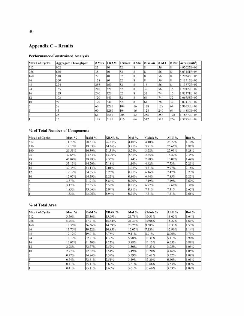
30
Appendix C – Results
Performance-Constrained Analysis
Max # of Cycles Aggregate Throughput # Mux # RAM # Xbars # Mul # Galois # ALU # Rot Area (units2) 512 902 23 40 52 8 8 56 8 4.92027E+06 256 646 38 40 52 8 8 56 8 5.03451E+06 160 518 72 40 52 8 8 56 8 5.29346E+06 96 360 128 80 52 8 8 56 8 7.11515E+06 48 224 256 160 52 8 16 56 8 1.13877E+07 24 155 240 320 52 8 32 56 16 1.79422E+07 16 129 240 320 52 8 32 74 16 1.82371E+07 12 103 120 640 52 8 64 74 32 3.06758E+07 10 97 120 640 52 8 64 78 32 3.07413E+07 6 58 60 1280 104 16 128 128 64 5.96530E+07 5 43 60 1280 104 16 128 240 64 6.14880E+07 3 25 64 2560 208 32 256 256 128 1.18879E+08 1 15 128 5120 416 64 512 512 256 2.37759E+08
% of Total Number of Components
Max # of Cycles Mux % RAM % XBAR % Mul % Galois % ALU % Rot % 512 11.79% 20.51% 26.67% 4.10% 4.10% 28.72% 4.10% 256 18.10% 19.05% 24.76% 3.81% 3.81% 26.67% 3.81% 160 29.51% 16.39% 21.31% 3.28% 3.28% 22.95% 3.28% 96 37.65% 23.53% 15.29% 2.35% 2.35% 16.47% 2.35% 48 46.04% 28.78% 9.35% 1.44% 2.88% 10.07% 1.44% 24 33.15% 44.20% 7.18% 1.10% 4.42% 7.73% 2.21% 16 32.35% 43.13% 7.01% 1.08% 4.31% 9.97% 2.16% 12 12.12% 64.65% 5.25% 0.81% 6.46% 7.47% 3.23% 10 12.07% 64.39% 5.23% 0.80% 6.44% 7.85% 3.22% 6 3.37% 71.91% 5.84% 0.90% 7.19% 7.19% 3.60% 5 3.17% 67.65% 5.50% 0.85% 6.77% 12.68% 3.38% 3 1.83% 73.06% 5.94% 0.91% 7.31% 7.31% 3.65% 1 1.83% 73.06% 5.94% 0.91% 7.31% 7.31% 3.65%
% of Total Area
Max # of Cycles Mux % RAM % XBAR % Mul % Galois % ALU % Rot % 512 3.56% 28.36% 15.69% 21.79% 10.31% 18.65% 1.64% 256 5.75% 27.71% 15.34% 21.30% 10.08% 18.22% 1.61% 160 10.36% 26.36% 14.59% 20.25% 9.58% 17.33% 1.53% 96 13.70% 39.22% 10.85% 15.07% 7.13% 12.90% 1.14% 48 17.12% 49.01% 6.78% 9.41% 8.91% 8.06% 0.71% 24 10.19% 62.21% 4.30% 5.98% 11.31% 5.11% 0.90% 16 10.02% 61.20% 4.23% 5.88% 11.13% 6.65% 0.89% 12 2.98% 72.77% 2.52% 3.50% 13.23% 3.95% 1.05% 10 2.97% 72.62% 2.51% 3.49% 13.20% 4.16% 1.05% 6 0.77% 74.84% 2.59% 3.59% 13.61% 3.52% 1.08% 5 0.74% 72.61% 2.51% 3.49% 13.20% 6.40% 1.05% 3 0.41% 75.11% 2.60% 3.61% 13.66% 3.53% 1.09% 1 0.41% 75.11% 2.60% 3.61% 13.66% 3.53% 1.09%

31
Area-Constrained Analysis
Max # of Cycles Aggregate Throughput # Mux # RAM # Xbars # Mul # Galois # ALU # Rot Area (units2) 512 902 23 40 52 8 8 56 8 4.92027E+06 256 646 38 40 52 8 8 56 8 5.03451E+06 128 518 72 40 52 8 8 56 8 5.29346E+06 128 297 122 40 53 8 16 81 58 7.11515E+06 64 156 73 84 113 8 33 141 74 1.13877E+07 32 92 64 192 105 17 64 135 64 1.79422E+07 32 93 68 192 156 16 32 197 129 1.82371E+07 16 55 64 320 209 16 129 262 129 3.06758E+07 16 55 69 321 208 17 128 256 132 3.07413E+07 16 38 136 387 459 68 258 608 283 5.96530E+07 8 28 146 774 208 64 161 541 261 6.14880E+07 8 23 204 828 521 182 514 1223 364 1.18879E+08 4 18 143 1282 789 930 523 1182 303 2.37759E+08
% of Total Number of Components
Max # of Cycles Mux % RAM % XBAR % Mul % Galois % ALU % Rot % 512 3.56% 28.36% 15.69% 21.79% 10.31% 18.65% 1.64% 256 5.75% 27.71% 15.34% 21.30% 10.08% 18.22% 1.61% 128 10.36% 26.36% 14.59% 20.25% 9.58% 17.33% 1.53% 128 13.06% 19.61% 11.06% 15.07% 14.26% 18.65% 8.24% 64 4.88% 25.73% 14.73% 9.41% 18.38% 20.29% 6.57% 32 2.72% 37.33% 8.69% 12.70% 22.62% 12.33% 3.60% 32 2.84% 36.72% 12.70% 11.76% 11.13% 17.70% 7.15% 16 1.59% 36.39% 10.12% 6.99% 26.67% 13.99% 4.25% 16 1.71% 36.42% 10.05% 7.41% 26.41% 13.64% 4.34% 16 1.74% 22.63% 11.42% 15.28% 27.43% 16.70% 4.79% 8 1.81% 43.91% 5.02% 13.95% 16.60% 14.42% 4.29% 8 1.31% 24.29% 6.51% 20.52% 27.42% 16.86% 3.09% 4 0.46% 18.81% 4.93% 52.42% 13.95% 8.15% 1.29%
% of Total Area
Max # of Cycles Mux % RAM % XBAR % Mul % Galois % ALU % Rot % 512 11.79% 20.51% 26.67% 4.10% 4.10% 28.72% 4.10% 256 18.10% 19.05% 24.76% 3.81% 3.81% 26.67% 3.81% 128 29.51% 16.39% 21.31% 3.28% 3.28% 22.95% 3.28% 128 32.28% 10.58% 14.02% 2.12% 4.23% 21.43% 15.34% 64 13.88% 15.97% 21.48% 1.52% 6.27% 26.81% 14.07% 32 9.98% 29.95% 16.38% 2.65% 9.98% 21.06% 9.98% 32 8.61% 24.30% 19.75% 2.03% 4.05% 24.94% 16.33% 16 5.67% 28.34% 18.51% 1.42% 11.43% 23.21% 11.43% 16 6.10% 28.38% 18.39% 1.50% 11.32% 22.63% 11.67% 16 6.18% 17.60% 20.87% 3.09% 11.73% 27.65% 12.87% 8 6.77% 35.92% 9.65% 2.97% 7.47% 25.10% 12.11% 8 5.32% 21.58% 13.58% 4.74% 13.40% 31.88% 9.49% 4 2.78% 24.88% 15.31% 18.05% 10.15% 22.94% 5.88%

32
Improved Area-Constrained Analysis
Max # of Cycles Aggregate Throughput # Mux # RAM # Xbars # Mul # Galois # ALU # Rot Area (units2) 512 902 23 40 52 8 8 56 8 4.92027E+06 256 646 38 40 52 8 8 56 8 5.03451E+06 128 518 72 40 52 8 8 56 8 5.29346E+06 128 297 120 40 52 8 16 78 48 6.93000E+06 32 156 60 160 52 8 16 128 32 1.13170E+07 16 103 60 320 52 8 32 128 32 1.79130E+07 16 98 60 320 52 8 32 128 64 1.82360E+07 16 57 64 384 104 16 128 196 128 3.01920E+07 16 57 120 384 104 16 128 196 128 3.06180E+07 8 30 128 768 208 32 256 388 128 5.90250E+07 8 29 128 768 208 32 256 388 256 6.03180E+07 4 18 128 1280 416 64 512 512 256 1.03820E+08 1 15 128 5120 416 64 512 512 256 2.37759E+08
% of Total Number of Components
Max # of Cycles Mux % RAM % XBAR % Mul % Galois % ALU % Rot % 512 3.56% 28.36% 15.69% 21.79% 10.31% 18.65% 1.64% 256 5.75% 27.71% 15.34% 21.30% 10.08% 18.22% 1.61% 128 10.36% 26.36% 14.59% 20.25% 9.58% 17.33% 1.53% 128 13.19% 20.13% 11.14% 15.47% 14.64% 18.44% 7.00% 32 4.04% 49.31% 6.82% 9.47% 8.97% 18.53% 2.86% 16 2.55% 62.31% 4.31% 5.99% 11.33% 11.71% 1.81% 16 2.51% 61.21% 4.23% 5.88% 11.13% 11.50% 3.55% 16 1.61% 44.36% 5.11% 7.10% 26.89% 10.64% 4.28% 16 2.98% 43.75% 5.04% 7.00% 26.51% 10.49% 4.22% 8 1.65% 45.38% 5.23% 7.27% 27.50% 10.77% 2.19% 8 1.62% 44.41% 5.12% 7.11% 26.91% 10.54% 4.29% 4 0.94% 43.00% 5.95% 8.26% 31.27% 8.08% 2.49% 1 0.41% 75.11% 2.60% 3.61% 13.66% 3.53% 1.09%
% of Total Area
Max # of Cycles Mux % RAM % XBAR % Mul % Galois % ALU % Rot % 512 11.79% 20.51% 26.67% 4.10% 4.10% 28.72% 4.10% 256 18.10% 19.05% 24.76% 3.81% 3.81% 26.67% 3.81% 128 29.51% 16.39% 21.31% 3.28% 3.28% 22.95% 3.28% 128 33.15% 11.05% 14.36% 2.21% 4.42% 21.55% 13.26% 32 13.16% 35.09% 11.40% 1.75% 3.51% 28.07% 7.02% 16 9.49% 50.63% 8.23% 1.27% 5.06% 20.25% 5.06% 16 9.04% 48.19% 7.83% 1.20% 4.82% 19.28% 9.64% 16 6.27% 37.65% 10.20% 1.57% 12.55% 19.22% 12.55% 16 11.15% 35.69% 9.67% 1.49% 11.90% 18.22% 11.90% 8 6.71% 40.25% 10.90% 1.68% 13.42% 20.34% 6.71% 8 6.29% 37.72% 10.22% 1.57% 12.57% 19.06% 12.57% 4 4.04% 40.40% 13.13% 2.02% 16.16% 16.16% 8.08% 1 1.83% 73.06% 5.94% 0.91% 7.31% 7.31% 3.65%

33
Appendix D – RaPiD-AES Components
4-Issue 8-bit Modulus 256/Galois Field Multiplier module mul8GalE( //Datapath Inputs XIn, YIn, //Datapath Outputs Output, //Control Inputs Mode, //Galois reduction polynomial (assume leading 1) GC7, GC6, GC5, GC4, GC3, GC2, GC1, GC0); //Performs unsigned %256 and 8-bit Galois field multiplication input [`BitWidth-1:0] XIn; input [`BitWidth-1:0] YIn; output [`BitWidth-1:0] Output; //Select Mode input Mode; //Reduction Polynomial (assume leading 1) input GC7; input GC6; input GC5; input GC4; input GC3; input GC2; input GC1; input GC0; reg [31:0] Output; reg [31:0] PP0; reg [31:0] PP1; reg [31:0] PP2; reg [31:0] PP3; reg [31:0] PP4; reg [31:0] PP5; reg [31:0] PP6; reg [31:0] PP7; reg [31:0] Mod8Result; reg [59:0] Galois1; reg [55:0] Galois2; reg [51:0] Galois3; reg [47:0] Galois4; reg [43:0] Galois5; reg [39:0] Galois6; reg [35:0] Galois7; reg [31:0] GaloisResult; //Field constant is actually 9'b1xxxxxxxx, but we assume leading 1 wire [7:0] GalConstant; assign GalConstant = {GC7, GC6, GC5, GC4, GC3, GC2, GC1, GC0}; always @(XIn or YIn or Mode) begin PP0 = {XIn[31:24] & {8{YIn[24]}}, XIn[23:16] & {8{YIn[16]}}, XIn[15:8] & {8{YIn[8]}}, XIn[7:0] & {8{YIn[0]}}}; PP1 = {XIn[31:24] & {8{YIn[25]}}, XIn[23:16] & {8{YIn[17]}}, XIn[15:8] & {8{YIn[9]}}, XIn[7:0] & {8{YIn[1]}}}; PP2 = {XIn[31:24] & {8{YIn[26]}}, XIn[23:16] & {8{YIn[18]}}, XIn[15:8] & {8{YIn[10]}}, XIn[7:0] & {8{YIn[2]}}}; PP3 = {XIn[31:24] & {8{YIn[27]}}, XIn[23:16] & {8{YIn[19]}}, XIn[15:8] & {8{YIn[11]}}, XIn[7:0] & {8{YIn[3]}}}; PP4 = {XIn[31:24] & {8{YIn[28]}}, XIn[23:16] & {8{YIn[20]}}, XIn[15:8] & {8{YIn[12]}}, XIn[7:0] & {8{YIn[4]}}}; PP5 = {XIn[31:24] & {8{YIn[29]}}, XIn[23:16] & {8{YIn[21]}}, XIn[15:8] & {8{YIn[13]}}, XIn[7:0] & {8{YIn[5]}}}; PP6 = {XIn[31:24] & {8{YIn[30]}}, XIn[23:16] & {8{YIn[22]}},
34
XIn[15:8] & {8{YIn[14]}}, XIn[7:0] & {8{YIn[6]}}}; PP7 = {XIn[31:24] & {8{YIn[31]}}, XIn[23:16] & {8{YIn[23]}}, XIn[15:8] & {8{YIn[15]}}, XIn[7:0] & {8{YIn[7]}}}; //Since we're producing all of the partial products out to 15 bits we could make //this a full 8-bit * 8-bit = 16-bit multiply if we want to Mod8Result = {(PP0[31:24] + {PP1[30:24], 1'd0} + {PP2[29:24], 2'd0} + {PP3[28:24], 3'd0} + {PP4[27:24], 4'd0} + {PP5[26:24], 5'd0} + {PP6[25:24], 6'd0} + {PP7[24], 7'd0}), (PP0[23:16] + {PP1[22:16], 1'd0} + {PP2[21:16], 2'd0} + {PP3[20:16], 3'd0} + {PP4[19:16], 4'd0} + {PP5[18:16], 5'd0} + {PP6[17:16], 6'd0} + {PP7[16], 7'd0}), (PP0[15:8] + {PP1[14:8], 1'd0} + {PP2[13:8], 2'd0} + {PP3[12:8], 3'd0} + {PP4[11:8], 4'd0} + {PP5[10:8], 5'd0} + {PP6[9:8], 6'd0} + {PP7[8], 7'd0}), (PP0[7:0] + {PP1[6:0], 1'd0} + {PP2[5:0], 2'd0} + {PP3[4:0], 3'd0} + {PP4[3:0], 4'd0} + {PP5[2:0], 5'd0} + {PP6[1:0], 6'd0} + {PP7[0], 7'd0})}; //Produces 15-bit "Product" Galois1 = {({7'd0, PP0[31:24]} ^ {6'd0, PP1[31:24], 1'd0} ^ {5'd0, PP2[31:24], 2'd0} ^ {4'd0, PP3[31:24], 3'd0} ^ {3'd0, PP4[31:24], 4'd0} ^ {2'd0, PP5[31:24], 5'd0} ^ {1'd0, PP6[31:24], 6'd0} ^ {PP7[31:24], 7'd0}), ({7'd0, PP0[23:16]} ^ {6'd0, PP1[23:16], 1'd0} ^ {5'd0, PP2[23:16], 2'd0} ^ {4'd0, PP3[23:16], 3'd0} ^ {3'd0, PP4[23:16], 4'd0} ^ {2'd0, PP5[23:16], 5'd0} ^ {1'd0, PP6[23:16], 6'd0} ^ {PP7[23:16], 7'd0}), ({7'd0, PP0[15:8]} ^ {6'd0, PP1[15:8], 1'd0} ^ {5'd0, PP2[15:8], 2'd0} ^ {4'd0, PP3[15:8], 3'd0} ^ {3'd0, PP4[15:8], 4'd0} ^ {2'd0, PP5[15:8], 5'd0} ^ {1'd0, PP6[15:8], 6'd0} ^ {PP7[15:8], 7'd0}), ({7'd0, PP0[7:0]} ^ {6'd0, PP1[7:0], 1'd0} ^ {5'd0, PP2[7:0], 2'd0} ^ {4'd0, PP3[7:0], 3'd0} ^ {3'd0, PP4[7:0], 4'd0} ^ {2'd0, PP5[7:0], 5'd0} ^ {1'd0, PP6[7:0], 6'd0} ^ {PP7[7:0], 7'd0})}; //Reduction Step 15->14 Galois2 = {(Galois1[58:45] ^ {({8{Galois1[59]}} & GalConstant), 6'd0}), (Galois1[43:30] ^ {({8{Galois1[44]}} & GalConstant), 6'd0}), (Galois1[28:15] ^ {({8{Galois1[29]}} & GalConstant), 6'd0}), (Galois1[13:0] ^ {({8{Galois1[14]}} & GalConstant), 6'd0})}; //Reduction Step14->13 Galois3 = {(Galois2[54:42] ^ {({8{Galois2[55]}} & GalConstant), 5'd0}), (Galois2[40:28] ^ {({8{Galois2[41]}} & GalConstant), 5'd0}), (Galois2[26:14] ^ {({8{Galois2[27]}} & GalConstant), 5'd0}), (Galois2[12:0] ^ {({8{Galois2[13]}} & GalConstant), 5'd0})}; //Reduction Step 13->12 Galois4 = {(Galois3[50:39] ^ {({8{Galois3[51]}} & GalConstant), 4'd0}), (Galois3[37:26] ^ {({8{Galois3[38]}} & GalConstant), 4'd0}), (Galois3[24:13] ^ {({8{Galois3[25]}} & GalConstant), 4'd0}), (Galois3[11:0] ^ {({8{Galois3[12]}} & GalConstant), 4'd0})}; //Reduction Step 12->11 Galois5 = {(Galois4[46:36] ^ {({8{Galois4[47]}} & GalConstant), 3'd0}), (Galois4[34:24] ^ {({8{Galois4[35]}} & GalConstant), 3'd0}), (Galois4[22:12] ^ {({8{Galois4[23]}} & GalConstant), 3'd0}), (Galois4[10:0] ^ {({8{Galois4[11]}} & GalConstant), 3'd0})}; //Reduction Step 11->10 Galois6 = {(Galois5[42:33] ^ {({8{Galois5[43]}} & GalConstant), 2'd0}), (Galois5[31:22] ^ {({8{Galois5[32]}} & GalConstant), 2'd0}), (Galois5[20:11] ^ {({8{Galois5[21]}} & GalConstant), 2'd0}), (Galois5[9:0] ^ {({8{Galois5[10]}} & GalConstant), 2'd0})}; //Reduction Step 10->9 Galois7 = {(Galois6[38:30] ^ {({8{Galois6[39]}} & GalConstant), 1'd0}), (Galois6[28:20] ^ {({8{Galois6[29]}} & GalConstant), 1'd0}), (Galois6[18:10] ^ {({8{Galois6[19]}} & GalConstant), 1'd0}), (Galois6[8:0] ^ {({8{Galois6[9]}} & GalConstant), 1'd0})}; //Reduction Step 9->8 GaloisResult = {(Galois7[34:27] ^ ({8{Galois7[35]}} & GalConstant)), (Galois7[25:18] ^ ({8{Galois7[26]}} & GalConstant)), (Galois7[16:9] ^ ({8{Galois7[17]}} & GalConstant)), (Galois7[7:0] ^ ({8{Galois7[8]}} & GalConstant))}; casex(Mode) //%256 Multiply 1'b0 : Output = Mod8Result; //Galois Multiply 1'b1 : Output = GaloisResult; endcase end endmodule

35
256 Byte Multi-mode RAM Unit module ramE(AddHi, AddLo, Input, Output, Mode, Clock, Length, Write); input Clock, Length, Write; input [`BitWidth-1:0] AddHi; input [`BitWidth-1:0] AddLo; input [`BitWidth-1:0] Input; output [`BitWidth-1:0] Output; //Select addressing mode input Mode; //3 addressing mode 256 Byte RAM reg [`BitWidth-1:0] Output; reg [3:0] ram_array7[63:0]; reg [3:0] ram_array6[63:0]; reg [3:0] ram_array5[63:0]; reg [3:0] ram_array4[63:0]; reg [3:0] ram_array3[63:0]; reg [3:0] ram_array2[63:0]; reg [3:0] ram_array1[63:0]; reg [3:0] ram_array0[63:0]; integer i; initial begin for(i=0; i<`MemWidth; i=i+1) begin ram_array7[i] = {4{1'b0}}; ram_array6[i] = {4{1'b0}}; ram_array5[i] = {4{1'b0}}; ram_array4[i] = {4{1'b0}}; ram_array3[i] = {4{1'b0}}; ram_array2[i] = {4{1'b0}}; ram_array1[i] = {4{1'b0}}; ram_array0[i] = {4{1'b0}}; end end always @(posedge Clock) begin if({Mode} == 1'b0) //8->8 Mode begin //This needs to be +2 since input may come from RAM which is +1 #(`ClkToOut + 2) Output[31:8] = 24'b0; casex(AddLo[7:6]) 2'b00: {Output[7:4], Output[3:0]} = {ram_array1[AddLo[5:0]],ram_array0[AddLo[5:0]]}; 2'b01: {Output[7:4], Output[3:0]} = {ram_array3[AddLo[5:0]],ram_array2[AddLo[5:0]]}; 2'b10: {Output[7:4], Output[3:0]} = {ram_array5[AddLo[5:0]],ram_array4[AddLo[5:0]]}; 2'b11: {Output[7:4], Output[3:0]} = {ram_array7[AddLo[5:0]],ram_array6[AddLo[5:0]]}; endcase end if({Mode} == 1'b1) //8 X 6->4 Mode begin #(`ClkToOut + 2) Output = {ram_array7[{AddHi[15:14], AddLo[31:28]}], ram_array6[{AddHi[13:12], AddLo[27:24]}], ram_array5[{AddHi[11:10], AddLo[23:20]}], ram_array4[{AddHi[9:8], AddLo[19:16]}], ram_array3[{AddHi[7:6], AddLo[15:12]}], ram_array2[{AddHi[5:4], AddLo[11:8]}], ram_array1[{AddHi[3:2], AddLo[7:4]}], ram_array0[{AddHi[1:0], AddLo[3:0]}]}; end end always @(negedge Clock) begin if (Write==1) begin if({Mode} == 1'b0) //Write in 6-bit addressing 32->32 begin ram_array7[AddLo[5:0]] = Input[31:28]; ram_array6[AddLo[5:0]] = Input[27:24]; ram_array5[AddLo[5:0]] = Input[23:20]; ram_array4[AddLo[5:0]] = Input[19:16]; ram_array3[AddLo[5:0]] = Input[15:12]; ram_array2[AddLo[5:0]] = Input[11:8]; ram_array1[AddLo[5:0]] = Input[7:4]; ram_array0[AddLo[5:0]] = Input[3:0]; end if({Mode} == 1'b1)
36
//Write in 2+4-bit addressing 32->32 begin ram_array7[{AddHi[1:0], AddLo[3:0]}] = Input[31:28]; ram_array6[{AddHi[1:0], AddLo[3:0]}] = Input[27:24]; ram_array5[{AddHi[1:0], AddLo[3:0]}] = Input[23:20]; ram_array4[{AddHi[1:0], AddLo[3:0]}] = Input[19:16]; ram_array3[{AddHi[1:0], AddLo[3:0]}] = Input[15:12]; ram_array2[{AddHi[1:0], AddLo[3:0]}] = Input[11:8]; ram_array1[{AddHi[1:0], AddLo[3:0]}] = Input[7:4]; ram_array0[{AddHi[1:0], AddLo[3:0]}] = Input[3:0]; end end end endmodule
Bi-Directional Shifter/Rotator module rotE(Input, DPSA, Output, SASource, Mode2, Mode1, Mode0, CPSA4, CPSA3, CPSA2, CPSA1, CPSA0); input [`BitWidth-1:0] Input; //Datapath Shift Amount input [`BitWidth-1:0] DPSA; output [`BitWidth-1:0] Output; //Select Shift Amount; input SASource; //Select Mode input Mode2; input Mode1; input Mode0; //Control Path Shift Amount input CPSA4; input CPSA3; input CPSA2; input CPSA1; input CPSA0; //Performs left/right rotate, logicial shift and arithmetic shift wire [4:0] ShiftAmount; //Top level has 63, followed by 47, 39, 35, 33, and finally 32 bits reg [4:0] Shift; reg [62:0] TopLevel; reg [46:0] ShiftBy16; reg [38:0] ShiftBy8; reg [34:0] ShiftBy4; reg [32:0] ShiftBy2; reg [31:0] Output; //SASource == 1 takes address from Control Path input assign ShiftAmount = (SASource==1'b1) ? {CPSA4, CPSA3, CPSA2, CPSA1, CPSA0} : DPSA; always @(Input or ShiftAmount or Mode2 or Mode1 or Mode0) begin casex({Mode2, Mode1, Mode0}) //Left Rot 3'b000 : {Shift, TopLevel} = {ShiftAmount[4:0], {Input[`BitWidth-1:0], Input[`BitWidth-1:1]}}; //Left Shift in 0's 3'b001 : {Shift, TopLevel} = {ShiftAmount[4:0], {Input[`BitWidth-1:0], 31'd0}}; //Left Shift in 1's 3'b010 : {Shift, TopLevel} = {ShiftAmount[4:0], {Input[`BitWidth-1:0], 31'd4294967295}}; 3'b011 : ; //Right Rot 3'b100 : {Shift, TopLevel} = {31 - ShiftAmount[4:0], {Input[`BitWidth-2:0], Input[`BitWidth-1:0]}}; //Right Logical Shift with 0's 3'b101 : {Shift, TopLevel} = {31 - ShiftAmount[4:0], {31'd0, Input[`BitWidth-1:0]}}; //Right Logical Shift with 1's 3'b110 : {Shift, TopLevel} = {31 - ShiftAmount[4:0], {31'd4294967295, Input[`BitWidth-1:0]}}; //Right Arithmetic Shift 3'b111 : {Shift, TopLevel} = {31 - ShiftAmount[4:0], {{`BitWidth-1{Input[`BitWidth-1]}}, Input[`BitWidth-1:0]}}; endcase //Shift 16 if(Shift[4]) ShiftBy16[46:0] = TopLevel[46:0]; else ShiftBy16[46:0] = TopLevel[62:16]; //Shift 8 if(Shift[3]) ShiftBy8[38:0] = ShiftBy16[38:0]; else ShiftBy8[38:0] = ShiftBy16[46:8]; //Shift 4 if(Shift[2])

37
ShiftBy4[34:0] = ShiftBy8[34:0]; else ShiftBy4[34:0] = ShiftBy8[38:4]; //Shift 2 if(Shift[1]) ShiftBy2[32:0] = ShiftBy4[32:0]; else ShiftBy2[32:0] = ShiftBy4[34:2]; //Shift 1 if(Shift[0]) Output[31:0] = ShiftBy2[31:0]; else Output[31:0] = ShiftBy2[32:1]; end endmodule
Crossbar module xBarE(In, Out, S159, S158, S157, S156, S155, S154, S153, S152, S151, S150, S149, S148, S147, S146, S145, S144, S143, S142, S141, S140, S139, S138, S137, S136, S135, S134, S133, S132, S131, S130, S129, S128, S127, S126, S125, S124, S123, S122, S121, S120, S119, S118, S117, S116, S115, S114, S113, S112, S111, S110, S109, S108, S107, S106, S105, S104, S103, S102, S101, S100, S99, S98, S97, S96, S95, S94, S93, S92, S91, S90, S89, S88, S87, S86, S85, S84, S83, S82, S81, S80, S79, S78, S77, S76, S75, S74, S73, S72, S71, S70, S69, S68, S67, S66, S65, S64, S63, S62, S61, S60, S59, S58, S57, S56, S55, S54, S53, S52, S51, S50, S49, S48, S47, S46, S45, S44, S43, S42, S41, S40, S39, S38, S37, S36, S35, S34, S33, S32, S31, S30, S29, S28, S27, S26, S25, S24, S23, S22, S21, S20, S19, S18, S17, S16, S15, S14, S13, S12, S11, S10, S9, S8, S7, S6, S5, S4, S3, S2, S1, S0); input [31:0] In; output [31:0] Out; input S159, S158, S157, S156, S155, S154, S153, S152, S151, S150; input S149, S148, S147, S146, S145, S144, S143, S142, S141, S140; input S139, S138, S137, S136, S135, S134, S133, S132, S131, S130; input S129, S128, S127, S126, S125, S124, S123, S122, S121, S120; input S119, S118, S117, S116, S115, S114, S113, S112, S111, S110; input S109, S108, S107, S106, S105, S104, S103, S102, S101, S100; input S99, S98, S97, S96, S95, S94, S93, S92, S91, S90; input S89, S88, S87, S86, S85, S84, S83, S82, S81, S80; input S79, S78, S77, S76, S75, S74, S73, S72, S71, S70; input S69, S68, S67, S66, S65, S64, S63, S62, S61, S60; input S59, S58, S57, S56, S55, S54, S53, S52, S51, S50; input S49, S48, S47, S46, S45, S44, S43, S42, S41, S40; input S39, S38, S37, S36, S35, S34, S33, S32, S31, S30; input S29, S28, S27, S26, S25, S24, S23, S22, S21, S20; input S19, S18, S17, S16, S15, S14, S13, S12, S11, S10; input S9, S8, S7, S6, S5, S4, S3, S2, S1, S0; //Allows any of the 32 input bits to be routed to any of the 32 output bits mux_32_to_1 mux0(In, {S4, S3, S2, S1, S0}, Out[0]); mux_32_to_1 mux1(In, {S9, S8, S7, S6, S5}, Out[1]); mux_32_to_1 mux2(In, {S14, S13, S12, S11, S10}, Out[2]); mux_32_to_1 mux3(In, {S19, S18, S17, S16, S15}, Out[3]); mux_32_to_1 mux4(In, {S24, S23, S22, S21, S20}, Out[4]); mux_32_to_1 mux5(In, {S29, S28, S27, S26, S25}, Out[5]); mux_32_to_1 mux6(In, {S34, S33, S32, S31, S30}, Out[6]); mux_32_to_1 mux7(In, {S39, S38, S37, S36, S35}, Out[7]); mux_32_to_1 mux8(In, {S44, S43, S42, S41, S40}, Out[8]); mux_32_to_1 mux9(In, {S49, S48, S47, S46, S45}, Out[9]); mux_32_to_1 mux10(In, {S54, S53, S52, S51, S50}, Out[10]); mux_32_to_1 mux11(In, {S59, S58, S57, S56, S55}, Out[11]); mux_32_to_1 mux12(In, {S64, S63, S62, S61, S60}, Out[12]); mux_32_to_1 mux13(In, {S69, S68, S67, S66, S65}, Out[13]); mux_32_to_1 mux14(In, {S74, S73, S72, S71, S70}, Out[14]); mux_32_to_1 mux15(In, {S79, S78, S77, S76, S75}, Out[15]); mux_32_to_1 mux16(In, {S84, S83, S82, S81, S80}, Out[16]); mux_32_to_1 mux17(In, {S89, S88, S87, S86, S85}, Out[17]); mux_32_to_1 mux18(In, {S94, S93, S92, S91, S90}, Out[18]); mux_32_to_1 mux19(In, {S99, S98, S97, S96, S95}, Out[19]); mux_32_to_1 mux20(In, {S104, S103, S102, S101, S100}, Out[20]); mux_32_to_1 mux21(In, {S109, S108, S107, S106, S105}, Out[21]); mux_32_to_1 mux22(In, {S114, S113, S112, S111, S110}, Out[22]); mux_32_to_1 mux23(In, {S119, S118, S117, S116, S115}, Out[23]); mux_32_to_1 mux24(In, {S124, S123, S122, S121, S120}, Out[24]); mux_32_to_1 mux25(In, {S129, S128, S127, S126, S125}, Out[25]); mux_32_to_1 mux26(In, {S134, S133, S132, S131, S130}, Out[26]); mux_32_to_1 mux27(In, {S139, S138, S137, S136, S135}, Out[27]); mux_32_to_1 mux28(In, {S144, S143, S142, S141, S140}, Out[28]); mux_32_to_1 mux29(In, {S149, S148, S147, S146, S145}, Out[29]); mux_32_to_1 mux30(In, {S154, S153, S152, S151, S150}, Out[30]);

38
mux_32_to_1 mux31(In, {S159, S158, S157, S156, S155}, Out[31]); endmodule

39
Appendix E – Example of RaPiD-AES Implementation: Rijndael
Primary Encryption code – Rijndael.rc #include "rijndael.h" StUnit(ramE, (Output), (), (AddHi, AddLo, Input), (Mode = 0, Write = 0)); CombUnit(xBarE, (Out), (), (In), (S159 = 0, S158 = 0, S157 = 0, S156 = 0, S155 = 0, S154 = 0, S153 = 0, S152 = 0, S151 = 0, S150 = 0, S149 = 0, S148 = 0, S147 = 0, S146 = 0, S145 = 0, S144 = 0, S143 = 0, S142 = 0, S141 = 0, S140 = 0, S139 = 0, S138 = 0, S137 = 0, S136 = 0, S135 = 0, S134 = 0, S133 = 0, S132 = 0, S131 = 0, S130 = 0, S129 = 0, S128 = 0, S127 = 0, S126 = 0, S125 = 0, S124 = 0, S123 = 0, S122 = 0, S121 = 0, S120 = 0, S119 = 0, S118 = 0, S117 = 0, S116 = 0, S115 = 0, S114 = 0, S113 = 0, S112 = 0, S111 = 0, S110 = 0, S109 = 0, S108 = 0, S107 = 0, S106 = 0, S105 = 0, S104 = 0, S103 = 0, S102 = 0, S101 = 0, S100 = 0, S99 = 0, S98 = 0, S97 = 0, S96 = 0, S95 = 0, S94 = 0, S93 = 0, S92 = 0, S91 = 0, S90 = 0, S89 = 0, S88 = 0, S87 = 0, S86 = 0, S85 = 0, S84 = 0, S83 = 0, S82 = 0, S81 = 0, S80 = 0, S79 = 0, S78 = 0, S77 = 0, S76 = 0, S75 = 0, S74 = 0, S73 = 0, S72 = 0, S71 = 0, S70 = 0, S69 = 0, S68 = 0, S67 = 0, S66 = 0, S65 = 0, S64 = 0, S63 = 0, S62 = 0, S61 = 0, S60 = 0, S59 = 0, S58 = 0, S57 = 0, S56 = 0, S55 = 0, S54 = 0, S53 = 0, S52 = 0, S51 = 0, S50 = 0, S49 = 0, S48 = 0, S47 = 0, S46 = 0, S45 = 0, S44 = 0, S43 = 0, S42 = 0, S41 = 0, S40 = 0, S39 = 0, S38 = 0, S37 = 0, S36 = 0, S35 = 0, S34 = 0, S33 = 0, S32 = 0, S31 = 0, S30 = 0, S29 = 0, S28 = 0, S27 = 0, S26 = 0, S25 = 0, S24 = 0, S23 = 0, S22 = 0, S21 = 0, S20 = 0, S19 = 0, S18 = 0, S17 = 0, S16 = 0, S15 = 0, S14 = 0, S13 = 0, S12 = 0, S11 = 0, S10 = 0, S9 = 0, S8 = 0, S7 = 0, S6 = 0, S5 = 0, S4 = 0, S3 = 0, S2 = 0, S1 = 0, S0 = 0)); CombUnit(mul8GalE, (Output), (), (XIn, YIn), (Mode = 0, //Reduction polynomial = 100011011 (assume leading 1) GC7 = 0, GC6 = 0, GC5 = 0, GC4 = 1, GC3 = 1, GC2 = 0, GC1 = 1, GC0 = 1)); CombUnit(rotE, (Output), (), (Input, DPSA), (SASource = 1, Mode2 = 0, Mode1 = 0, Mode0 = 0, CPSA4 = 0, CPSA3 = 0, CPSA2 = 0, CPSA1 = 0, CPSA0 = 0)); void encrypt(Word input[INPUT_SIZE], Word cipherText[NUM_BLOCKS * WORDS_PER_BLOCK]){ Ram subkeysA, subkeysB, subkeysC, subkeysD; ramE RAMA3, RAMA2, RAMA1, RAMA0; ramE RAMB3, RAMB2, RAMB1, RAMB0; ramE RAMC3, RAMC2, RAMC1, RAMC0; ramE RAMD3, RAMD2, RAMD1, RAMD0; Ram plainTextA, plainTextB, plainTextC, plainTextD; Ram outA, outB, outC, outD; //Pipeline variables Word St0, St1, St2, St3, St4, St5, St6, St7, St8; //Constants Word constant3s, constant2s; Word constantByte3, constantByte2, constantByte1, constantByte0; //Internal temp variables Word feedBackA, feedBackB, feedBackC, feedBackD; //Key Addition temp Word KAA, KAB, KAC, KAD; //Byte Substitution temp variables Word BSIA3, BSIA2, BSIA1; Word BSIB3, BSIB2, BSIB1; Word BSIC3, BSIC2, BSIC1; Word BSID3, BSID2, BSID1; Word BSOA3, BSOA2, BSOA1, BSOA0; Word BSOB3, BSOB2, BSOB1, BSOB0; Word BSOC3, BSOC2, BSOC1, BSOC0; Word BSOD3, BSOD2, BSOD1, BSOD0; //Shift Row temp variables Word SRA, SRB, SRC, SRD; //Mix Column temp variables Word MCIA3, MCIA2, MCIA1, MCIA0; Word MCIB3, MCIB2, MCIB1, MCIB0; Word MCIC3, MCIC2, MCIC1, MCIC0; Word MCID3, MCID2, MCID1, MCID0; Word MCA, MCB, MCC, MCD; Word tempAddress; Word tempWord; For fillBlock, fillStage, fillConstants, computeBlock, compute, output, outputWord; Seq { // Load from input stream for(fillBlock = 0; fillBlock < 64; fillBlock++){ for(fillStage = 0; fillStage < 9; fillStage++){ Datapath{ if(fillBlock.first && fillStage.first){ //Initalize

40
subkeysA.address = 0; subkeysB.address = 0; subkeysC.address = 0; subkeysD.address = 0; tempAddress = 0; RAMA3.AddHi = 0; RAMA2.AddHi = 0; RAMA1.AddHi = 0; RAMA0.AddHi = 0; RAMB3.AddHi = 0; RAMB2.AddHi = 0; RAMB1.AddHi = 0; RAMB0.AddHi = 0; RAMC3.AddHi = 0; RAMC2.AddHi = 0; RAMC1.AddHi = 0; RAMC0.AddHi = 0; RAMD3.AddHi = 0; RAMD2.AddHi = 0; RAMD1.AddHi = 0; RAMD0.AddHi = 0; plainTextA.address = 0; plainTextB.address = 0; plainTextC.address = 0; plainTextD.address = 0; } //Fill Pipe St0 = St1; St1 = St2; St2 = St3; St3 = St4; St4 = St5; St5 = St6; St6 = St7; St7 = St8; St8 = input[(fillBlock * 9) + fillStage]; if(fillStage.last){ RAMA3.Write = 1; RAMA2.Write = 1; RAMA1.Write = 1; RAMA0.Write = 1; RAMB3.Write = 1; RAMB2.Write = 1; RAMB1.Write = 1; RAMB0.Write = 1; RAMC3.Write = 1; RAMC2.Write = 1; RAMC1.Write = 1; RAMC0.Write = 1; RAMD3.Write = 1; RAMD2.Write = 1; RAMD1.Write = 1; RAMD0.Write = 1; RAMA3.AddLo = tempAddress; RAMA2.AddLo = tempAddress; RAMA1.AddLo = tempAddress; RAMA0.AddLo = tempAddress; RAMB3.AddLo = tempAddress; RAMB2.AddLo = tempAddress; RAMB1.AddLo = tempAddress; RAMB0.AddLo = tempAddress; RAMC3.AddLo = tempAddress; RAMC2.AddLo = tempAddress; RAMC1.AddLo = tempAddress; RAMC0.AddLo = tempAddress; RAMD3.AddLo = tempAddress; RAMD2.AddLo = tempAddress; RAMD1.AddLo = tempAddress; RAMD0.AddLo = tempAddress; //Load Data //First load 128-bit subkey subkeysA = St0; subkeysB = St1; subkeysC = St2; subkeysD = St3; //Then 8-bit substitution box RAMA3.Input = St4; RAMA2.Input = St4; RAMA1.Input = St4; RAMA0.Input = St4; RAMB3.Input = St4; RAMB2.Input = St4; RAMB1.Input = St4; RAMB0.Input = St4; RAMC3.Input = St4; RAMC2.Input = St4; RAMC1.Input = St4; RAMC0.Input = St4; RAMD3.Input = St4; RAMD2.Input = St4; RAMD1.Input = St4; RAMD0.Input = St4; //Then 1 128-bit plaintext block plainTextA = St5; plainTextB = St6; plainTextC = St7; plainTextD = St8; //Update addresses; subkeysA.address++; subkeysB.address++; subkeysC.address++; subkeysD.address++; tempAddress = tempAddress + 1; plainTextA.address++; plainTextB.address++; plainTextC.address++; plainTextD.address++; } } } } for(fillConstants = 0; fillConstants < 2; fillConstants++){ Datapath{ //Fill Pipe St0 = St1; St1 = input[(64 * 9) + fillConstants]; if(fillConstants.last){ constant2s = St0; constant3s = St1; } } } //Do the computation for(computeBlock = 0; computeBlock < NUM_BLOCKS; computeBlock++){ for(compute = 0; compute < NUM_ROUNDS; compute++){ Datapath{ //Initialize input and output memories if(computeBlock.first && compute.first){ outA.address = 0; outB.address = 0; outC.address = 0; outD.address = 0; plainTextA.address = 0; plainTextB.address = 0; plainTextC.address = 0; plainTextD.address = 0; } //First round has Input Whitening if(compute.first){ //Initialize subkey memory subkeysA.address = 0; subkeysB.address = 0; subkeysC.address = 0; subkeysD.address = 0; feedBackA = plainTextA; feedBackB = plainTextB; feedBackC = plainTextC; feedBackD = plainTextD; } //Every round has a Key Addition step KAA = feedBackA ^ subkeysA; KAB = feedBackB ^ subkeysB; KAC = feedBackC ^ subkeysC; KAD = feedBackD ^ subkeysD; //Every round except last one has a Byte Substitution step

41
if(!compute.last){ //Perform rotations for addresses //BSIX3 = KAX >> 24 ((BSIA3), ()) = rotE((KAA, 0), (1, 1, 0, 1, 1, 1, 0, 0, 0)); ((BSIB3), ()) = rotE((KAB, 0), (1, 1, 0, 1, 1, 1, 0, 0, 0)); ((BSIC3), ()) = rotE((KAC, 0), (1, 1, 0, 1, 1, 1, 0, 0, 0)); ((BSID3), ()) = rotE((KAD, 0), (1, 1, 0, 1, 1, 1, 0, 0, 0)); //BSIX2 = KAX >> 16 ((BSIA2), ()) = rotE((KAA, 0), (1, 1, 0, 1, 1, 0, 0, 0, 0)); ((BSIB2), ()) = rotE((KAB, 0), (1, 1, 0, 1, 1, 0, 0, 0, 0)); ((BSIC2), ()) = rotE((KAC, 0), (1, 1, 0, 1, 1, 0, 0, 0, 0)); ((BSID2), ()) = rotE((KAD, 0), (1, 1, 0, 1, 1, 0, 0, 0, 0)); //BSIX1 = KAX >> 8 ((BSIA1), ()) = rotE((KAA, 0), (1, 1, 0, 1, 0, 1, 0, 0, 0)); ((BSIB1), ()) = rotE((KAB, 0), (1, 1, 0, 1, 0, 1, 0, 0, 0)); ((BSIC1), ()) = rotE((KAC, 0), (1, 1, 0, 1, 0, 1, 0, 0, 0)); ((BSID1), ()) = rotE((KAD, 0), (1, 1, 0, 1, 0, 1, 0, 0, 0)); //Perform lookup RAMA3.AddLo = BSIA3; RAMA2.AddLo = BSIA2; RAMA1.AddLo = BSIA1; RAMA0.AddLo = KAA; RAMB3.AddLo = BSIB3; RAMB2.AddLo = BSIB2; RAMB1.AddLo = BSIB1; RAMB0.AddLo = KAB; RAMC3.AddLo = BSIC3; RAMC2.AddLo = BSIC2; RAMC1.AddLo = BSIC1; RAMC0.AddLo = KAC; RAMD3.AddLo = BSID3; RAMD2.AddLo = BSID2; RAMD1.AddLo = BSID1; RAMD0.AddLo = KAD; BSOA3 = RAMA3.Output; BSOA2 = RAMA2.Output; BSOA1 = RAMA1.Output; BSOA0 = RAMA0.Output; BSOB3 = RAMB3.Output; BSOB2 = RAMB2.Output; BSOB1 = RAMB1.Output; BSOB0 = RAMB0.Output; BSOC3 = RAMC3.Output; BSOC2 = RAMC2.Output; BSOC1 = RAMC1.Output; BSOC0 = RAMC0.Output; BSOD3 = RAMD3.Output; BSOD2 = RAMD2.Output; BSOD1 = RAMD1.Output; BSOD0 = RAMD0.Output; //Shift Row //A = A3 || B2 || C1 || D0 ((BSOA3), ()) = rotE((BSOA3, 0), (1, 0, 0, 1, 1, 1, 0, 0, 0)); ((BSOB2), ()) = rotE((BSOB2, 0), (1, 0, 0, 1, 1, 0, 0, 0, 0)); ((BSOC1), ()) = rotE((BSOC1, 0), (1, 0, 0, 1, 0, 1, 0, 0, 0)); SRA = BSOA3 | BSOB2 | BSOC1 | BSOD0; //B = B3 || C2 || D1 || A0 ((BSOB3), ()) = rotE((BSOB3, 0), (1, 0, 0, 1, 1, 1, 0, 0, 0)); ((BSOC2), ()) = rotE((BSOC2, 0), (1, 0, 0, 1, 1, 0, 0, 0, 0)); ((BSOD1), ()) = rotE((BSOD1, 0), (1, 0, 0, 1, 0, 1, 0, 0, 0)); SRB = BSOB3 | BSOC2 | BSOD1 | BSOA0; //C = C3 || D2 || A1 || B0 ((BSOC3), ()) = rotE((BSOC3, 0), (1, 0, 0, 1, 1, 1, 0, 0, 0)); ((BSOD2), ()) = rotE((BSOD2, 0), (1, 0, 0, 1, 1, 0, 0, 0, 0)); ((BSOA1), ()) = rotE((BSOA1, 0), (1, 0, 0, 1, 0, 1, 0, 0, 0)); SRC = BSOC3 | BSOD2 | BSOA1 | BSOB0; //D = D3 || A2 || B1 || C0 ((BSOD3), ()) = rotE((BSOD3, 0), (1, 0, 0, 1, 1, 1, 0, 0, 0)); ((BSOA2), ()) = rotE((BSOA2, 0), (1, 0, 0, 1, 1, 0, 0, 0, 0)); ((BSOB1), ()) = rotE((BSOB1, 0), (1, 0, 0, 1, 0, 1, 0, 0, 0)); SRD = BSOD3 | BSOA2 | BSOB1 | BSOC0; } //Every round but last two have Mix Column step if(compute < NUM_ROUNDS - 2){ //X = (X <<< 24) + (X <<< 16) + 3(X <<<8) + 2X ((MCIA3), ()) = rotE((SRA, 0), (1, 0, 0, 0, 1, 1, 0, 0, 0)); ((MCIA2), ()) = rotE((SRA, 0), (1, 0, 0, 0, 1, 0, 0, 0, 0)); ((MCIA1), ()) = rotE((SRA, 0), (1, 0, 0, 0, 0, 1, 0, 0, 0)); ((MCIA1), ()) = mul8GalE((MCIA1, constant3s), (1)); ((MCIA0), ()) = mul8GalE((SRA, constant2s), (1)); feedBackA = MCIA3 ^ MCIA2 ^ MCIA1 ^ MCIA0; ((MCIB3), ()) = rotE((SRB, 0), (1, 0, 0, 0, 1, 1, 0, 0, 0)); ((MCIB2), ()) = rotE((SRB, 0), (1, 0, 0, 0, 1, 0, 0, 0, 0)); ((MCIB1), ()) = rotE((SRB, 0), (1, 0, 0, 0, 0, 1, 0, 0, 0)); ((MCIB1), ()) = mul8GalE((MCIB1, constant3s), (1)); ((MCIB0), ()) = mul8GalE((SRB, constant2s), (1)); feedBackB = MCIB3 ^ MCIB2 ^ MCIB1 ^ MCIB0; ((MCIC3), ()) = rotE((SRC, 0), (1, 0, 0, 0, 1, 1, 0, 0, 0)); ((MCIC2), ()) = rotE((SRC, 0), (1, 0, 0, 0, 1, 0, 0, 0, 0)); ((MCIC1), ()) = rotE((SRC, 0), (1, 0, 0, 0, 0, 1, 0, 0, 0)); ((MCIC1), ()) = mul8GalE((MCIC1, constant3s), (1)); ((MCIC0), ()) = mul8GalE((SRC, constant2s), (1)); feedBackC = MCIC3 ^ MCIC2 ^ MCIC1 ^ MCIC0; ((MCID3), ()) = rotE((SRD, 0), (1, 0, 0, 0, 1, 1, 0, 0, 0)); ((MCID2), ()) = rotE((SRD, 0), (1, 0, 0, 0, 1, 0, 0, 0, 0)); ((MCID1), ()) = rotE((SRD, 0), (1, 0, 0, 0, 0, 1, 0, 0, 0)); ((MCID1), ()) = mul8GalE((MCID1, constant3s), (1)); ((MCID0), ()) = mul8GalE((SRD, constant2s), (1)); feedBackD = MCID3 ^ MCID2 ^ MCID1 ^ MCID0; } //Second to last round needs to loop shift row result if(compute == NUM_ROUNDS - 2){ feedBackA = SRA; feedBackB = SRB; feedBackC = SRC; feedBackD = SRD; }

42
if(compute.last){ outA = KAA; outB = KAB; outC = KAC; outD = KAD; outA.address++; outB.address++; outC.address++; outD.address++; plainTextA.address++; plainTextB.address++; plainTextC.address++; plainTextD.address++; } subkeysA.address ++; subkeysB.address ++; subkeysC.address ++; subkeysD.address ++; } } } // Output Results // We could parallelize this to run as soon as the results are ready // but due to ram addressing conflicts, we need to output after the // calculations are completely done for(output = 0; output < NUM_BLOCKS; output++){ for(outputWord = 0; outputWord < WORDS_PER_BLOCK; outputWord++){ Datapath{ if(output.first && outputWord.first){ outA.address = 0; outB.address = 0; outC.address = 0; outD.address = 0; } if(outputWord == 0) tempWord = outA; else if(outputWord == 1) tempWord = outB; else if(outputWord == 2) tempWord = outC; else tempWord = outD; cipherText[(output * 4) + outputWord] = tempWord; if(outputWord.last){ outA.address++; outB.address++; outC.address++; outD.address++; } } } } } }
Header File – Rijndael.h #define STAGES 1 #include "rapidb.h" #define NUM_SUBKEYS 11 #define WORDS_PER_KEY 4 #define SBOX_SIZE 256 #define LOOKUP_PER_SBOX 8 #define NUM_BLOCKS 4 #define WORDS_PER_BLOCK 4 #define INPUT_SIZE ((64 * 9) + 2) #define NUM_ROUNDS 11 #define HEX_PER_WORD 8 #define SBOX_OFFSET NUM_SUBKEYS * WORDS_PER_KEY #define PLAINTEXT_OFFSET (NUM_SUBKEYS * WORDS_PER_KEY) + (SBOX_SIZE * 8)
C Wrapper Function and Verification Code – testRijndael.cc #include <assert.h> #include <stdio.h> #include <iostream.h> #include <fstream.h> #include <iomanip.h> #include <stdlib.h> #include "rijndael.h" void encrypt(Word *, Word*); void render(char* head, Word x, char* tail) { unsigned long temp; printf("%s", head); temp = x & 4294967295; printf("%08x", temp); printf("%s", tail); } void transpose(Word array[4]){ //Reorganize bytes to be column major, not row major //0 1 2 3 0 4 8 12

43
//4 5 6 7 => 1 5 9 13 //8 9 10 11 2 6 10 14 //12 13 14 15 3 7 11 15 int i, j, temp; int byteArray[4][4]; for(i = 0; i < 4; i++){ for(j = 0; j < 4; j++){ byteArray[i][j] = (array[i] >> 24 - (j * 8)) & 255; } } for(i = 0; i < 4; i++){ array[i] = 0; for(j = 0; j < 4; j++){ array[i] += byteArray[j][i] << 24 - (j * 8); } } } int main() { // These subkeys are were produced from the key // 000102030405060708090A0B0C0D0E0F const char asciiSubkeys[NUM_SUBKEYS][WORDS_PER_KEY][HEX_PER_WORD + 1] = { {"00010203", "04050607", "08090A0B", "0C0D0E0F"}, {"D6AA74FD", "D2AF72FA", "DAA678F1", "D6AB76FE"}, {"B692CF0B", "643DBDF1", "BE9BC500", "6830B3FE"}, {"B6FF744E", "D2C2C9BF", "6C590CBF", "0469BF41"}, {"47F7F7BC", "95353E03", "F96C32BC", "FD058DFD"}, {"3CAAA3E8", "A99F9DEB", "50F3AF57", "ADF622AA"}, {"5E390F7D", "F7A69296", "A7553DC1", "0AA31F6B"}, {"14F9701A", "E35FE28C", "440ADF4D", "4EA9C026"}, {"47438735", "A41C65B9", "E016BAF4", "AEBF7AD2"}, {"549932D1", "F0855768", "1093ED9C", "BE2C974E"}, {"13111D7F", "E3944A17", "F307A78B", "4D2B30C5"}}; // This are the 8 S-boxes for the forward encrytion const int sBox [SBOX_SIZE] = { 99, 124, 119, 123, 242, 107, 111, 197, 48, 1, 103, 43, 254, 215, 171, 118, 202, 130, 201, 125, 250, 89, 71, 240, 173, 212, 162, 175, 156, 164, 114, 192, 183, 253, 147, 38, 54, 63, 247, 204, 52, 165, 229, 241, 113, 216, 49, 21, 4, 199, 35, 195, 24, 150, 5, 154, 7, 18, 128, 226, 235, 39, 178, 117, 9, 131, 44, 26, 27, 110, 90, 160, 82, 59, 214, 179, 41, 227, 47, 132, 83, 209, 0, 237, 32, 252, 177, 91, 106, 203, 190, 57, 74, 76, 88, 207, 208, 239, 170, 251, 67, 77, 51, 133, 69, 249, 2, 127, 80, 60, 159, 168, 81, 163, 64, 143, 146, 157, 56, 245, 188, 182, 218, 33, 16, 255, 243, 210, 205, 12, 19, 236, 95, 151, 68, 23, 196, 167, 126, 61, 100, 93, 25, 115, 96, 129, 79, 220, 34, 42, 144, 136, 70, 238, 184, 20, 222, 94, 11, 219, 224, 50, 58, 10, 73, 6, 36, 92, 194, 211, 172, 98, 145, 149, 228, 121, 231, 200, 55, 109, 141, 213, 78, 169, 108, 86, 244, 234, 101, 122, 174, 8, 186, 120, 37, 46, 28, 166, 180, 198, 232, 221, 116, 31, 75, 189, 139, 138, 112, 62, 181, 102, 72, 3, 246, 14, 97, 53, 87, 185, 134, 193, 29, 158, 225, 248, 152, 17, 105, 217, 142, 148, 155, 30, 135, 233, 206, 85, 40, 223, 140, 161, 137, 13, 191, 230, 66, 104, 65, 153, 45, 15, 176, 84, 187, 22}; const char asciiPlainText[NUM_BLOCKS][WORDS_PER_BLOCK][HEX_PER_WORD + 1] = { {"00010203", "04050607", "08090A0B", "0C0D0E0F"}, {"100F0E0D", "0C0B0A09", "08070605", "04030201"}, {"00020406", "01030500", "02040601", "03050002"}, {"00030609", "0C020508", "0B010407", "0A000306"}}; const char asciiCipherText[NUM_BLOCKS][WORDS_PER_BLOCK][HEX_PER_WORD + 1] = { {"0A940BB5", "416EF045", "F1C39458", "C653EA5A"}, {"20C2FF67", "36789ECD", "3B81D366", "75DD1442"}, {"95BFD2DB", "A04F6D98", "4EDCEDBE", "68DC4AB7"}, {"5033731B", "E0EC208D", "5E3338FF", "19C2CE04"}}; Word subkeys[NUM_SUBKEYS] [WORDS_PER_KEY]; Word sBoxMem [SBOX_SIZE / 4]; Word plainText[NUM_BLOCKS][WORDS_PER_BLOCK]; Word inputStream[INPUT_SIZE]; Word cipherText[NUM_BLOCKS * WORDS_PER_BLOCK]; Word organizedCT[NUM_BLOCKS][WORDS_PER_BLOCK]; Word checkText[NUM_BLOCKS][WORDS_PER_BLOCK]; Word tempText; int i, j, k, m, errors;

44
char * tempCharP; //Translate subkeys to hex for(i = 0; i < NUM_SUBKEYS; i++){ for(j = 0; j < WORDS_PER_KEY; j++){ subkeys[i][j] = strtoul(asciiSubkeys[i][j], &tempCharP, 16); } } //Transpose bytes for(i = 0; i < NUM_SUBKEYS; i++){ //transpose(subkeys[i]); } //Repackage the s-box contents for(i = 0; i < SBOX_SIZE/4; i++){ sBoxMem[i] = 0; sBoxMem[i] = sBox[i]; for(j = 1; j < 4; j++){ sBoxMem[i] += sBox[i + (64 * j)] << (8 * j); } } //Translate plaintext into hex for(i = 0; i < NUM_BLOCKS; i++){ for(j = 0; j < WORDS_PER_BLOCK; j++){ plainText[i][j] = strtoul(asciiPlainText[i][j], &tempCharP, 16); } } //Transpose bytes for(i = 0; i < NUM_BLOCKS; i++){ //transpose(plainText[i]); } //Translate known correct ciphertext into hex for(i = 0; i < NUM_BLOCKS; i++){ for(j = 0; j < WORDS_PER_BLOCK; j++){ checkText[i][j] = strtoul(asciiCipherText[i][j], &tempCharP, 16); } } //Load into inputStream column-wise, not row-wise (All A's, all B's, etc) for(i = 0; i < 64; i++){ inputStream[i * 9] = subkeys[i % NUM_SUBKEYS][0]; inputStream[(i * 9) + 1] = subkeys[i % NUM_SUBKEYS][1]; inputStream[(i * 9) + 2] = subkeys[i % NUM_SUBKEYS][2]; inputStream[(i * 9) + 3] = subkeys[i % NUM_SUBKEYS][3]; inputStream[(i * 9) + 4] = sBoxMem[i]; inputStream[(i * 9) + 5] = plainText[i % NUM_BLOCKS][0]; inputStream[(i * 9) + 6] = plainText[i % NUM_BLOCKS][1]; inputStream[(i * 9) + 7] = plainText[i % NUM_BLOCKS][2]; inputStream[(i * 9) + 8] = plainText[i % NUM_BLOCKS][3]; } //Add constant 2's and 3's inputStream[(64 * 9)] = 33686018; inputStream[(64 * 9) + 1] = 50529027; //Initialize output to easily detect verilog problem for(i = 0; i < NUM_BLOCKS * WORDS_PER_BLOCK; i++){ cipherText[i] = 9; } for(i = 0; i < NUM_BLOCKS; i++){ printf("CHECKTEXT [%d] = \t", i); for(j = 0; j < WORDS_PER_BLOCK; j++){ render("", checkText[i][j], " "); } printf("\n"); } printf("\n"); encrypt(inputStream, cipherText); //Transpose back for(i = 0; i < NUM_BLOCKS; i++){ for(j = 0; j < WORDS_PER_BLOCK; j++){ organizedCT[i][j] = cipherText[(i * WORDS_PER_BLOCK) + j]; } } for(i = 0; i < NUM_BLOCKS; i++){ //transpose(organizedCT[i]); } //Check Output errors = 0; for(i = 0; i < NUM_BLOCKS; i++){ printf("Ciphertext [%d] = \t", i); for(j = 0; j < WORDS_PER_BLOCK; j++){ render("", organizedCT[i] [j], " ");

45
if(checkText[i][j] != organizedCT[i][j]) errors++; } printf(" --- %d ERRORS\n", errors); errors = 0; } }