ece 327: digital systems engineering solutions to …ece327/course-notes/tut-soln.pdfece 327:...
TRANSCRIPT

ECE 327: Digital Systems EngineeringSolutions to Tutorial Problems
2018t1 (Winter)
Mark Aagaard
University of WaterlooDepartment of Electrical and Computer Engineering

ece327: 2018t1 (Winter)0.0 1 ii

Contents
1 Fundamentals of VHDL 51.1 IEEE 1164 . . . . . . . . . . . . . . . . . . . . . . . . . . . . . . . . . . . . . . . 51.2 VHDL Syntax . . . . . . . . . . . . . . . . . . . . . . . . . . . . . . . . . . . . . 61.3 Flops, Latches, and Combinational Circuitry . . . . . . . . . . . . . . . . . . . . . 91.4 Delta-Cycle Simulation: Pong . . . . . . . . . . . . . . . . . . . . . . . . . . . . 111.5 Delta-Cycle Simulation: Befuddle . . . . . . . . . . . . . . . . . . . . . . . . . . 141.6 Synflopsys Simulation Algorithm . . . . . . . . . . . . . . . . . . . . . . . . . . . 151.7 VHDL — VHDL Behavioural Comparison: Teradactyl . . . . . . . . . . . . . . . 171.8 The Good, the Bad, and the Synthesizably Challenged . . . . . . . . . . . . . . . . 171.9 Hardware — VHDL Comparison . . . . . . . . . . . . . . . . . . . . . . . . . . 20
2 Additional Features of VHDL 21
3 Overview of FPGAs 233.1 2-bit adder . . . . . . . . . . . . . . . . . . . . . . . . . . . . . . . . . . . . . . . 233.2 Number of FPGA Cells for Arithmetic Code . . . . . . . . . . . . . . . . . . . . . 253.3 Number of FPGA Cells for Schematic . . . . . . . . . . . . . . . . . . . . . . . . 28
4 Introduction to RTL Design 314.1 FSM: A-Count . . . . . . . . . . . . . . . . . . . . . . . . . . . . . . . . . . . . 314.2 Start-Stop A-Count . . . . . . . . . . . . . . . . . . . . . . . . . . . . . . . . . . 324.3 Count-Sequence Design . . . . . . . . . . . . . . . . . . . . . . . . . . . . . . . . 34
5 Dataflow Diagrams 375.1 Dataflow Diagram Optimization . . . . . . . . . . . . . . . . . . . . . . . . . . . 385.2 Michener: Design and Optimization . . . . . . . . . . . . . . . . . . . . . . . . . 395.3 Allocation and Control Table . . . . . . . . . . . . . . . . . . . . . . . . . . . . . 405.4 Control Table Optimization . . . . . . . . . . . . . . . . . . . . . . . . . . . . . . 425.5 Inter-Parcel Variables . . . . . . . . . . . . . . . . . . . . . . . . . . . . . . . . . 485.6 Code Review . . . . . . . . . . . . . . . . . . . . . . . . . . . . . . . . . . . . . 495.7 Sketches of Problems . . . . . . . . . . . . . . . . . . . . . . . . . . . . . . . . . 52
6 Advanced Design 556.1 Pipelining and Dataflow Diagrams . . . . . . . . . . . . . . . . . . . . . . . . . . 566.2 Overlapping Pipeline Stages . . . . . . . . . . . . . . . . . . . . . . . . . . . . . 58
iii

CONTENTS iv
7 Performance Analysis and Optimization 637.1 Farmer . . . . . . . . . . . . . . . . . . . . . . . . . . . . . . . . . . . . . . . . . 637.2 Network and Router . . . . . . . . . . . . . . . . . . . . . . . . . . . . . . . . . . 647.3 Performance Short Answer . . . . . . . . . . . . . . . . . . . . . . . . . . . . . . 677.4 Microprocessors . . . . . . . . . . . . . . . . . . . . . . . . . . . . . . . . . . . . 677.5 Multiply Instruction . . . . . . . . . . . . . . . . . . . . . . . . . . . . . . . . . . 707.6 FPGA vs CPU . . . . . . . . . . . . . . . . . . . . . . . . . . . . . . . . . . . . . 737.7 Waterluvian on New FPGA Chip . . . . . . . . . . . . . . . . . . . . . . . . . . . 78
8 Timing Analysis 818.1 Terminology . . . . . . . . . . . . . . . . . . . . . . . . . . . . . . . . . . . . . . 828.2 Hold Time Violations . . . . . . . . . . . . . . . . . . . . . . . . . . . . . . . . . 838.3 Latch Analysis . . . . . . . . . . . . . . . . . . . . . . . . . . . . . . . . . . . . 848.4 Latch Analysis . . . . . . . . . . . . . . . . . . . . . . . . . . . . . . . . . . . . 858.5 Critical Path and False Path . . . . . . . . . . . . . . . . . . . . . . . . . . . . . . 888.6 Critical Path . . . . . . . . . . . . . . . . . . . . . . . . . . . . . . . . . . . . . . 888.7 YACP: Yet Another Critical Path . . . . . . . . . . . . . . . . . . . . . . . . . . . 898.8 Timing Models . . . . . . . . . . . . . . . . . . . . . . . . . . . . . . . . . . . . 908.9 Elmore Analysis of Super-Vias . . . . . . . . . . . . . . . . . . . . . . . . . . . . 928.10 Zeraf . . . . . . . . . . . . . . . . . . . . . . . . . . . . . . . . . . . . . . . . . . 958.11 Short Answer . . . . . . . . . . . . . . . . . . . . . . . . . . . . . . . . . . . . . 978.12 Worst Case Conditions and Derating Factor . . . . . . . . . . . . . . . . . . . . . 98
9 Power Analysis and Power-Aware Design 1019.1 Short Answers . . . . . . . . . . . . . . . . . . . . . . . . . . . . . . . . . . . . . 1019.2 VLSI Gurus . . . . . . . . . . . . . . . . . . . . . . . . . . . . . . . . . . . . . . 1039.3 Advertising Ratios . . . . . . . . . . . . . . . . . . . . . . . . . . . . . . . . . . 1049.4 Vary Supply Voltage . . . . . . . . . . . . . . . . . . . . . . . . . . . . . . . . . 1049.5 Clock Gating . . . . . . . . . . . . . . . . . . . . . . . . . . . . . . . . . . . . . 1059.6 Clock Speed Increase Without Power Increase . . . . . . . . . . . . . . . . . . . . 1079.7 Power Reduction Strategies . . . . . . . . . . . . . . . . . . . . . . . . . . . . . . 1089.8 State Encoding . . . . . . . . . . . . . . . . . . . . . . . . . . . . . . . . . . . . 1109.9 Power Consumption on New Chip . . . . . . . . . . . . . . . . . . . . . . . . . . 112

Chapter 1
Fundamentals of VHDL
1.1 IEEE 1164
For each of the values in the list below, answer whether or not it is defined in the ieee.std_logic_1164library. If it is part of the library, write a 2–3 word description of the value.
Values: ’-’, ’#’, ’0’, ’1’, ’A’, ’h’, ’H’, ’L’, ’Q’, ’X’, ’Z’.
Answer:
In std logic 1164?Yes No Description
’-’ X don’t care’#’ X’0’ X strong 0’1’ X strong 1’A’ X’h’ X’H’ X weak 1’L’ X weak 0’Q’ X’X’ X strong unknown’Z’ X high impedance
NOTE: ’h’ is not in the package, because characters are case sensitive. Forexample ’a’ is different than ’A’.
5

1.2. VHDL SYNTAX 6
1.2 VHDL Syntax
Answer whether each of the VHDL code fragments q2a through q2f is legal VHDL code.
NOTES: 1) “...” represents a fragment of legal VHDL code.2) For full marks, if the code is illegal, you must explain why.
q2a architecture main of anchiceratops issignal a, b, c : std_logic;
beginprocess begin
wait until rising_edge(c);a <= if (b = ’1’) then
...else
...end if;
end process;end main;
ILLEGAL: if-then-else is a state-ment, not an expression, you can’t put itif-then-else on right-hand-side of as-signment since it doesn’t produce a valueto assign to signal a.
q2b architecture main of tulerpeton isbegin
lab: for i in 15 downto 0 loop...
end loop;end main;
ILLEGAL: loop statements are sequential,while architecture bodies contain concur-rent statements.

7 CHAPTER 1. FUNDAMENTALS OF VHDL
q2c architecture main of metaxygnathus issignal a : std_logic;
beginlab: if (a = ’1’) generate
...end generate;
end main;
ILLEGAL: condition for if-generatestatements must be statically determined;testing the value of a signal is dynamic.
q2d architecture main of temnospondyl iscomponent compa
port (a : in std_logic;b : out std_logic
);end component;signal p, q : std_logic;
begincoma_1 : compa
port map (a => p, b => q);...
end main;
LEGAL

1.2. VHDL SYNTAX 8
q2e architecture main of pachyderm isfunction inv(a : std_logic)
return std_logic isbegin
return(NOT a);end inv;signal p, b : std_logic;
beginp <= inv(b => a);...
end main;
ILLEGAL: the argument to inv shouldbe (a => b). In function calls andcomponent instantiations, when usingnamed parameter instantiation (as op-posed to positional parameter instantia-tion), the syntax is formal => actual.In the problem, the function definition is:inv( a : std logic ) and the functioncall is: inv( a => b). Here a is theformal argument and b is the actual argu-ment, so the correct function call would be:inv( a => b )
q2f architecture main of apatosaurus istype state_ty is (S0, S1, S2);signal st : state_ty;signal p : std_logic;
begincase st is
when S0 | S1 => p <= ’0’;when others => p <= ’1’;
end case;end main;
ILLEGAL: case statements are sequential;but the body of an architecture containsconcurrent statements.

9 CHAPTER 1. FUNDAMENTALS OF VHDL
1.3 Flops, Latches, and Combinational Circuitry
For each of the signals p...z in the architecture main of montevido, answer whether the signalis a latch, combinational gate, or flip-flop.
entity montevido isport (
a, b0, b1, c0, c1, d0, d1, e0, e1 : in std_logic;l : in std_logic_vector (1 downto 0);p, q, r, s, u, v, y, z : out std_logic
);end montevido;
architecture main of montevido issignal i, j, t, w, x : std_logic;
begin
i <= c0 xor c1;j <= c0 and c1;
process (a, i, j) beginif (a = ’1’) then
p <= i and j;else
p <= not i;end if;
end process;
process (a, b0, b1) beginif rising_edge(a) then
q <= b0 and b1;end if;
end process;
process(a, c0, c1, d0, d1, e0, e1)
beginif (a = ’1’) then
r <= c0 or c1;s <= d0 and d1;
elser <= e0 xor e1;
end if;end process;
process beginwait until rising_edge(a);t <= b0 xor b1;u <= not t;v <= not x;
end process;
process beginwait until rising_edge(a);case l is
when "00" =>w <= b0 and b1;x <= ’0’;
when "01" =>w <= ’-’;x <= ’1’;
when others =>w <= c0 xor c1;x <= ’-’;
end case;end process;
y <= c0 xor c1;z <= x xor w;
end main;

1.3. FLOPS, LATCHES, AND COMBINATIONAL CIRCUITRY 10
Answer:
Latch Combinational Flip-flopp Xq Xr Xs Xt Xu Xv Xw Xx Xy Xz X
Explanation of why e, which is the output of a flip-flop, have a value at 5ns,which is before the first rising edge of the clock.
Before the first rising edge of the clock, the following assignments will allhappen:
a <= ’0’;b <= ’0’;...----------- end of delta cycled <= ’0’...----------- end of delta cyclee <= d;
If you were to implement VHDL code in hardware, e would be the output of aflop, and as such would remain as ’U’ until the first rising edge of the clock.This is a situation where simulating the VHDL code will have slightly differentresults than simulating the hardware. Most questions in ece327 that ask youto compare the behaviour of VHDL code with the behaviour of a circuit willsay to focus on the steady-state behaviour and ignore any differences in thefirst few clock cycles.
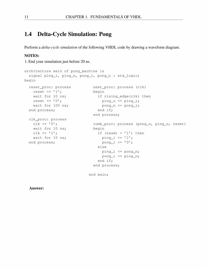
11 CHAPTER 1. FUNDAMENTALS OF VHDL
1.4 Delta-Cycle Simulation: Pong
Perform a delta-cycle simulation of the following VHDL code by drawing a waveform diagram.
NOTES:1. End your simulation just before 20 ns.
architecture main of pong_machine issignal ping_i, ping_n, pong_i, pong_n : std_logic;
begin
reset_proc: processreset <= ’1’;wait for 10 ns;reset <= ’0’;wait for 100 ns;
end process;
clk_proc: processclk <= ’0’;wait for 10 ns;clk <= ’1’;wait for 10 ns;
end process;
next_proc: process (clk)begin
if rising_edge(clk) thenping_n <= ping_i;pong_n <= pong_i;
end if;end process;
comb_proc: process (pong_n, ping_n, reset)begin
if (reset = ’1’) thenping_i <= ’1’;pong_i <= ’0’;
elseping_i <= pong_n;pong_i <= ping_n;
end if;end process;
end main;
Answer:

1.4. DELTA-CYCLE SIMULATION: PONG 12
reset
clk
ping_i
ping_n
pong_i
pong_n
next_proc
comb_proc
reset_proc
clk_proc
Tim
e
Sim
rou
nd
s
Sim
cy
cles
0ns
U U U U U U U U U U UU
ES
ES
R
ES
10ns
RE
S
δδ
δ
RR R R
U
U
ES
UU U
U
ES
RE
S
U U
U
U
U U
RE
S
RE
S
RE
S
U
U
U
U
U U
RE
S
U U
U
U
UU
20ns
δδ

13 CHAPTER 1. FUNDAMENTALS OF VHDL

1.5. DELTA-CYCLE SIMULATION: BEFUDDLE 14
1.5 Delta-Cycle Simulation: Befuddle
Perform a delta-cycle simulation of the following VHDL code by drawing a waveform diagram.
NOTES:1. Begin your simulation at 5 ns using the value shown for each signal.2. End your simulation just before 15 ns;
entity befuddle isend entity;
architecture main of befuddle issignal clk, a, b, c, d, e, f : std_logic;
begin
proc_clk: processbegin
clk <= ’0’;wait for 10 ns;clk <= ’1’;wait for 10 ns;
end process;
proc_extern : processbegin
a <= ’0’;b <= ’0’;wait for 5 ns;a <= ’1’;b <= ’1’;wait for 15 ns;
end process;
proc_1 : process (a, b, c)begin
c <= a and b;d <= a xor c;
end process;
proc_2 : processbegin
wait until rising_edge(clk);e <= d;
end process;
proc_3 : process (c, e) beginf <= c xor e;
end process;
end architecture;
Answer:

15 CHAPTER 1. FUNDAMENTALS OF VHDL
clk
a
b
c
d
e
f
proc_1
proc_2
proc_3
proc_clk
proc_extern
Time
Sim rounds
Sim cycles
5ns
0
0
0
0
0
0
0
0
0
U
U
U
U
0
R E S
R E S R E S
R E S
U U
10ns
R E S
δ δ δ
R E S
U
U
R E S
δ δ δ
15ns
U
U
Note: the instruction to end just before 15 ns simply causes us to stop thesimulation just before 15 ns. The values on the signals at the end of 10 ns willremain until the next event, which happens at 20 ns.
1.6 Synflopsys Simulation Algorithm
You have been hired by a small software startup company, Synflopsys, that is creating a newsimulator for VHDL programs. The main feature of the simulator is that the value of each signalwill be computed at most once per simulation round.

1.6.1 Advantage 16
1.6.1 Advantage
What would be the most important advantage of the Synflopsys simulator over a standard delta-cycle simulator?
Answer:
Faster simulation runs. By computing the value of each signal at most onceper simulation round, the time to run a simulation will be decreased.
1.6.2 Compatibility
For which VHDL programs could the proposed simulator give the same simulation results at eachreal moment in time (e.g., each nanosecond) as a standard VHDL delta-cycle simulator?
Answer:
VHDL programs without combinational loops.
1.6.3 Zero-Delay Simulation Rules
List the two fundamental rules that zero-delay simulators must obey, and then briefly hypothesizehow the Synflopsys simulator attempts to achieve these rules.
Answer:
Rule 1 The gates execute in parallelHypothesis Because there are no combinational loops, there is a topological
order among the signals, and the values can be computed in topologicalorder.
Rule 2 Events must propagate instantaneously through combinationalcircuitry.
Hypothesis Because each signal changes its value at most once permoment in time, increment time at the end of each iteration of computingthe signals in topological order. There is no need for delta cycles or otherinfinitesimally small increments of time.

17 CHAPTER 1. FUNDAMENTALS OF VHDL
1.7 VHDL — VHDL Behavioural Comparison: Teradactyl
For each of the VHDL architectures q3a through q3c, does the signal v have the same behaviouras it does in the main architecture of teradactyl?
NOTES: 1) For full marks, if the code has different behaviour, you must explainwhy.
2) Ignore any differences in behaviour in the first few clock cycles that iscaused by initialization of flip-flops, latches, and registers.
3) All code fragments in this question are legal, synthesizable VHDL code.
entity teradactyl isport (
a : in std_logic;v : out std_logic
);end teradactyl;architecture main of teradactyl is
signal m : std_logic;begin
m <= a;v <= m;
end main;
architecture q3a of teradactyl issignal b, c, d : std_logic;
beginb <= a;c <= b;d <= c;v <= d;
end q3a;
SAME - Intermediate signals are optimized out.
architecture q3b of teradactyl issignal m : std_logic;
beginprocess (a, m) begin
v <= m;m <= a;
end process;end q3b;
SAME - Putting it in a process doesn’t matter.
architecture q3c of teradactyl issignal m : std_logic;
beginprocess (a) begin
m <= a;end process;process (m) begin
v <= m;end process;
end q3c;
SAME - Putting it in a seperate process doesn’tmatter due to the parallel nature of VHDL.
1.8 The Good, the Bad, and the Synthesizably Challenged
For each of the code fragments below, answer the following questions.

1.8. THE GOOD, THE BAD, AND THE SYNTHESIZABLY CHALLENGED 18
NOTES:1. Is the code legal VHDL?2. If the code is legal VHDL:
(a) Answer whether the code is synthesizable.(b) If the code is synthesizable, answer whether it adheres to good coding practices, according to
the guidelines for E&CE 327.
3. If the the code is not legal, not synthesizable, or does not follow good coding practices, explainwhy.
P1.8.1process beginwait until rising_edge(clk);if (sum = 5) or (reset = ’1’) then
state <= S0;sum <= to_unsigned(0, 8);
elsesum <= a + b;if state = S0 then
state <= S1;end if;
end if;end process;
Answer:legal, synth, good
P1.8.2process (reset, sum) begin
if (sum = 5) or (reset = ’1’) thenstate <= S0;
elsestate <= S1;
end if;end process;process (state, a, b) begin
if state = S0 thensum <= to_unsigned(0, 8);
elsesum <= a + b;
end if;end process;
Answer:legal, synth, bad : comb loop

19 CHAPTER 1. FUNDAMENTALS OF VHDL
P1.8.3process begin
wait until rising_edge(clk);if (sum = 5) or (reset = ’1’) then
state <= S0;else
state <= S1;end if;
end process;gen0 : if state = S0 generate
sum <= to_unsigned(0, 8);end generate;gen1 : if state /= S0 generate
sum <= a + b;end generate;
Answer:illegal: if-genererate with dynamic
condition
P1.8.4process begin
wait until rising_edge(clk);if reset = ’1’ then
state <= S0;sum <= to_unsigned(0, 8);
end if;end process;process (clk) begin
if rising_edge(clk) thenstate <= next_state;
end if;end process;process (sum) begin
if sum = 5 thennext_state <= S0;
elsenext_state <= S1;
end if;end process;process (state, a, b) begin
if state = S0 thensum <= to_unsigned(0, 8);
elsesum <= a + b;
end if;end process;
Answer:legal, synth, bad: two drivers of
signals

1.9. HARDWARE — VHDL COMPARISON 20
1.9 Hardware — VHDL Comparison
For each of the circuits q2a–q2d, answerwhether the signal d has the same behaviouras it does in the main architecture of q2.
entity q2 isport (
a, clk, reset : in std_logic;d : out std_logic
);end q2;architecture main of q2 is
signal b, c : std_logic;begin
b <= ’0’ when (reset = ’1’)else a;
process (clk) beginif rising_edge(clk) then
c <= b;d <= c;
end if;end process;
end main;
q2a
clk
a
0
reset
dq2b
clk
a
0
reset
d
q2c
clk
a
0
reset
d
q2d
clk
a
0
reset
d
clk
Answer:q2a: a shouldn’t be flopped. q2b: One too many FFs. q2c: Correct
operation. q2d: This will work (i.e. it has the same input-outputcharacteristics) but the internal description is different.

Chapter 2
Additional Features of VHDL
The material in this chapter is useful for the labs. It will not be tested on exams.
21

22

Chapter 3
Overview of FPGAs
3.1 2-bit adder
This question compares an FPGA and generic-gates implementation of 2-bit full adder.
3.1.1 Generic Gates
Show the implementation of a 2 bit adder using NAND, NOR, and NOT gates.
3.1.2 FPGA
Show the implementation of a 2 bit adder using generic FPGA cells; show the equations for thelookup tables.
Answer:
23

3.1.2 FPGA 24
CE
S
R D Q
c_in
comb
sum[0]
CE
S
R D Q
comb
a[0] b[0]
a[1] b[1]
sum[1]
c_out
carry_1

25 CHAPTER 3. OVERVIEW OF FPGAS
3.2 Number of FPGA Cells for Arithmetic Code
Calculate the minimum number of FPGA cells needed to implement the VHDL code below.
NOTES:1. The signals ab sel and cd sel are std logic.2. The signals a, b, c, d, e, k, m, n, p, and z are 12-bit unsigned.3. The inputs to the system are: a, b, c, d, e, ab sel, cd sel,4. The output from the system is: z.5. Optimizations are allowed, so long as the externally visible input-to-output behaviour of the
system does not change.6. For full marks, you must justify your answer with a drawing and/or text.
k <= a when ab sel = ’1’ else b;m <= c when cd sel = ’1’ else d;process (clk) beginif rising_edge(clk) then
n <= k + m;p <= e;z <= n + p;
end if;end process;
Answer:
Original circuit:
a
b
c
d
ab_sel
cd_sel
k
m
n
e p
z
Optimized circuit:

3.2. NUMBER OF FPGA CELLS FOR ARITHMETIC CODE 26
a
b
c
d
ab_sel
cd_sel
k
m
n
e
zs
LUTs flops num LUTs flopssignal circuitry per bit per bit bits total totaln mux and adder 1 0 12 12 0s mux and adder, reg 1 1 12 12 12z reg 0 1 12 0 12
Total 24 24
Total number of cells = Max(24 LUTs, 24 flops) = 24 cells.
We can put a 2:1 mux and an adder in the same LUT.
Each cell has a LUT and a flip-flop, so we can fit both the adder and the regfor z into one cell per bit.
Optimized circuit option:
Using a dataflow diagram (covered in Chapter 5), we can reuse the adder andmux in two clock cycles.

27 CHAPTER 3. OVERVIEW OF FPGAS
0
0
ab_sel a b e cd_sel c d
a1 m1
r1 r2
z
a1
r1
LUTs flops num LUTs flopssignal circuitry per bit per bit bits total totala1 mux and adder 1 0 12 12 0m1 mux 1 0 12 12 0r1 reg 0 1 12 0 12r2 reg 0 1 12 0 12
Total 24 24

3.3. NUMBER OF FPGA CELLS FOR SCHEMATIC 28
3.3 Number of FPGA Cells for Schematic
Design an FPGA implementation of the gate-level circuit shown below that uses the minimumnumber of FPGA cells. Use the FPGA cells on the following page to answer the question.
NOTES:1. The primary inputs of the circuit are: a, b, c, d, e, f.2. The primary outputs of the circuit are: r, o, v, z.3. Do not perform any logic optimizations.4. For each FPGA cell that you use:• Label the input and output ports of the cell using the signal names from the gate-level circuit
for ports that you use and NC (for no-connect) for ports that you don’t use.• Show the configuration for the internal multiplexer by connecting either the PLA or input port
of the cell to the flop.
Answer:
The gray boxes describe how the signals are used. For example, “m1” is thefirst input to the PLA that drives m and “id” is the D-input to the flop that drivesi.
d
e
f
g
h
i
j
k
l
n
o
p
m
q
s
t
u
v
w y z x zd
y1y2
y3
y4
v1
v3
v2
v4l2
l1
r1r2
r3
r4
m1
m2
m3
id
id
c
b
a r

29 CHAPTER 3. OVERVIEW OF FPGAS
z
y
ro
h y
o
m
l
f
NC
NC
a
b
c
NC
NC
i
a
b
c
NC
m
e
l
d
h v
o
m
d
h
NC
NC
NC
i
a
NC
NC
NC
NC
NC

3.3. NUMBER OF FPGA CELLS FOR SCHEMATIC 30

Chapter 4
Introduction to RTL Design
4.1 FSM: A-Count
The state-machines below are supposed to count the number of contiguous clock cycles in whicha=’1’.•Assume that a=’0’ for the first three clock cycles.• For each state-machine, answer whether the machine works correctly.• If the machine works correctly, answer what the latency through the system is.• If the machine does not work correctly, describe how its behaviour differs from the specification.
Sample waveform for a machine with a latency of 1 clock cycle.
a
z 0 1 2 3 00 0 1 2 00
Sample waveform for a machine with a latency of 2 clock cycles.
a
z 0 1 2 3 00 0 1 2 00 0
4.1a
S0
z’ = 0;
a z’ = z + 1;!a z’ = 0;
OK, latency = 1
4.1b
S0
z’ = 0;
a z’ = z + 1;!a
OK, latency = 1
31

4.2. START-STOP A-COUNT 32
4.1c
S0
z’ = 0;
a
z’ = z + 1;
!a
S1
z’ = 0;
OK, latency = 2
4.1d
S0
z’ = 0;
a z’ = z + 1;!a
S1
z’ = 0;
OK, latency = 1. NOTE: relies upon as-sumption that a=’0’ in first clock cycle,otherwise, z is not initialiazed for first se-quence of a=’1’.
4.1e
S2
z’ = 0;
a
z’ = z + 1;
!a
S1
z’ = 0;
S0
BUG: samples a every-other clock cycle.
4.1f
S0 S1
z’ = 0; z’ = z + 1;
a!a a!a
OK: latency = 2
4.2 Start-Stop A-Count
Each of the three state machines on the next page is intended to meet the system description below:1. The inputs to the system are: start, stop, and a. The output is z.2. In the first clock cycle, start and stop are both guaranteed to be ’0’.3. The counting shall begin in the clock cycle after start=’1’.4. The counting shall continue up to, but not including, the next clock cycle in which stop=’1’.5. The current values of start, stop, and a shall affect z in the next clock cycle.6. In the clock cycle after stop=’1’, the output z shall be set to 0 and shall remain 0 until the
next sequence of counting begins.7. The system may put a constraint on the inputs such that there is a minimum gap of clock cycles
between stop=’1’ and the next start=’1’. Each state machine may have its own value forthe minimum gap. The minimum gap may be as small as 0 clock cycles.

33 CHAPTER 4. INTRODUCTION TO RTL DESIGN
start
stop
a
z 0 1 2 3 1 1
z is updated each cycle,
beginning after start=’1’
and stopping when stop=’1’
stop=’1’ has no effect if not counting
a=’1’ has no effect if not counting
start=’1’ has no effect in the
middle of a counting sequence
0 0
start
stop
a
z 0 1 0 02 1 0 0 0 0
0 0 0
counting sequence
0 0 0
0 40 10
gap=5gap=2
gap=0
1 2 0
NOTES:1. If the state machine is correct, answer what the minimum gap value is.2. If the state machine is incorrect, explain either how the machines behaviour differs from the
system description or how the state machine could be modified to fix the incorrect behaviour.

4.3. COUNT-SEQUENCE DESIGN 34
4.2.1
Answer:Incorrect.
Explanation: Whena=’1’, the output z isupdated in the currentclock cycle. It shouldbe updated in the nextclock cycle.
S0!s
tart
a
!a
S1stop
!stopz=0 z=0 start
z=x
z = x+1x’=z
x’=0
4.2.2
Answer:Correct. Gap=0.
Explanation: z isinitialized in the firstclock cycle and whenstop=’1’. Whenstop=’1’, start issampled in the sameclock cycle.
S0!s
tart
start
z’=0
!sta
rt
a
!a
S1
stop
!stop
z’ = z+1
z’=0
start
4.2.3
Answer:Incorrect.
Explanation (required):The input a is notsampled every clockcycle during thecounting sequence.
startS1
stop
S3
z’ = 0
z’ = 0z’=z+1S2
!stop
a
!a
S0!s
tart
4.3 Count-Sequence Design
Design a state machine that counts the number of times a=’1’, beginning when start=’1’ andending when stop=’1’.
NOTES:

35 CHAPTER 4. INTRODUCTION TO RTL DESIGN
1. The inputs to the system are: start, stop, and a. The output is z.2. In the first clock cycle, start and stop are both guaranteed to be ’0’.3. In the first clock cycle, the output z shall be set to 0.4. The counting shall begin in a clock cycle in which start=’1’.5. The counting shall continue up to and including a clock cycle in which stop=’1’.6. The output z shall be updated according to the values of start, stop, and a in the current
clock cycle.7. In the clock cycle after stop=’1’, the output z shall be set to 0 and shall remain 0 until the
next sequence of counting begins.8. Marks will be based on correct functionality, elegance of the design, and clarity of the drawing.
start
stop
a
z 0 1 2 3 10 0 0
z is updated each cycle,
beginning when start=’1’
and continuing until stop=’1’
stop=’1’ has no effect if not counting
a=’1’ has no effect if not counting
start=’1’ in the middle of a counting
sequence starts a new sequence
0 0
start
stop
a
z 0 1 2 3 0 0 02 3 3 1 2 0 0 0 0
2 0 0 0 0 0
counting sequence
Answer:

4.3. COUNT-SEQUENCE DESIGN 36
S0
count’=0
!start
z=0
start
a
nxt_count = prev_count+1
count’ = nxt_count
z = nxt_count
stop
!a
z=prev_count
S1
!stop
prev_count = 0prev_count = count
start !start
count’=0

Chapter 5
Dataflow Diagrams
37

5.1. DATAFLOW DIAGRAM OPTIMIZATION 38
5.1 Dataflow Diagram Optimization
Use the dataflow diagram below to answer sections 5.1.1 and 5.1.2.
F
F
a b c
d
G
F
G
e
z
5.1.1 Resource Usage
List the number of items for each resource used in the dataflow diagram.
Answer:
input ports 3output ports 1registers 2f components 2g components 1

39 CHAPTER 5. DATAFLOW DIAGRAMS
5.1.2 Optimization
Draw an optimized dataflow diagram that reduces the total execution time and produces the sameoutput values without increasing the area. Or, if the performance cannot be improved withoutincreasing area, describe the limiting factor on the performance.
NOTES:• you may change the times when signals are read from the environment• you may not increase the resource usage (input ports, registers, output ports, f components, g
components)• you may not increase the clock period
Answer:
f
f
a b
c
d
g
f
g
e
5.2 Michener: Design and Optimization
Design a circuit named michener that performs the following operation: z = (a+d) + ((b -c) - 1)
NOTES:1. Inputs shall be combinational.2. Outputs shall be registered.3. Optimize your design for area.4. You may schedule the inputs to arrive at any time.5. You may do algebraic transformations of the specification.

5.3. ALLOCATION AND CONTROL TABLE 40
Answer:
z
a
+
+
d b c
1
Data-dependency graph
z
+
+
1
b
a
d
c
Dataflow diagram
5.3 Allocation and Control Table
5.3.1 Allocation
For the dataflow diagram below, perform: input/output allocation, datapath allocation, and registerallocation.
• You may not change the allocations that have already been done.
• You may use 2:1 multiplexers, and may combine 2:1 multiplexers to create larger multiplex-ers. (e.g. two 2:1 muxes can be combined to create a 3:1 multiplexer)
• Optimization goals in order of highest priority to lowest:1. Minimize the number of adders2. Minimize the number of input and output ports3. Minimize the number of registers4. Minimize the number of 2:1 multiplexers (including the 2:1 muxes used to build larger
multiplexers)

41 CHAPTER 5. DATAFLOW DIAGRAMS
• You may not perform any algebraic or scheduling optimizations on the dataflow diagram.
Answer:
a b
+
+
+
c
+
+
d
+
+
x z
r1 r2 r3
a1 a2
i1 i2 i3
a1
a2
a2
a3
a3
r3 r1 r2 r4
r1 r2 r3
r3
r4
r1 r2
y
S0
S1
S2
S3
S0
i3
Obsolete: should use combinational inputs
and registered outputs.
Answer:There are several allocations
that arrive at the following result:
Number of input ports 3Number of output ports 3Number of adders 3Number of registers 4Number of 2:1 multiplexers 5
5.3.2 Control Tables
Draw the register and datapath control tables for your dataflow diagram. Leave the “don’t care”symbols in the table, that is, do not do don’t-care optimization.
Answer:
r1 r2 r3 r4 a1 a2 a3ce d ce d ce d ce d src1 src2 src1 src2 src1 src2
S0 1 i1 1 i2 1 i3 – – – – – – – –S1 1 a1 0 – 1 i3 1 a2 r1 r2 r2 r3 – –S2 1 a1 1 a2 1 a3 0 – r1 r3 r2 r3 a1 r4S3 0 – 1 a2 1 a3 – – – – r2 r3 r2 r4

5.4. CONTROL TABLE OPTIMIZATION 42
5.4 Control Table Optimization
In this question, you will optimize control tables, then design the hardware that implements thecontrol table. section 5.4.1 is for a one-hot encoding and section 5.4.2 is for a binary encoding.
NOTES:1. Inputs: i1 and i2. Data registers: r1, r2, and r3. Datapath components: add1,sub1.
2. State signal: st (see encoding information with section 5.4.1 and section 5.4.2).3. Your first goal is to minimize area, then optimize for clock speed without increasing area.4. Your circuit may be implemented with any number of the following gates, where the area of
each gate is shown in the table below:Gate Area= (2-bits) 8= (4-bits) 20
Gate AreaAND 2OR 2NOT 1
5. You may not change the behaviour of either the registers or the outputs of the adder or subtracter.6. You may not add any registers.7. As a guide when filling out your answers, the blank control tables contain the values from the
original table printed in grey.
Original control table:
r1 r2 r3 add1 sub1d ce d ce d ce src1 src2 src1 src2
S0 i1 1 – 0 i2 1 r3 r2 – –S1 r3 1 add1 1 – 0 r1 r3 r2 add1S2 r3 1 – – i2 1 r3 r1 add1 r2S3 – – add1 1 r1 1 r1 r3 – –
In each of section 5.4.1 and section 5.4.2, after optimizing the control table, use the VHDL func-tions AND, OR, and NOT to write expressions to implement each signal in terms of the state signaland, if helpful, the other control signals.
NOTES:1. For the “else” case of if-then-elses used as multiplexers, write “others”.2. If a control signal or case for a mux is not needed, write “N/A”.

43 CHAPTER 5. DATAFLOW DIAGRAMS
Example
To illustrate how to write your answers, this example shows a sample answer and theequivalent VHDL code, which you do not have to write.
Your Answerr99 d sel r99 <= r80 when : not(a and b)
r99 <= r81 when : others
Equivalent VHDL
r99_d_sel = not(a and b);...if r99_d_sel = ’1’ thenr99 <= r80;
elser99 <= r81;
end if;

5.4.1 One-Hot Encoding 44
5.4.1 One-Hot Encoding
subtype state_ty : std logic vector( 3 downto 0 );signal st : state_ty;constant S0 : state_ty := "0001";constant S1 : state_ty := "0010";constant S2 : state_ty := "0100";constant S3 : state_ty := "1000";
Answer:
Original table:
r1 r2 r3 add1 sub1d ce d ce d ce src1 src2 src1 src2
S0 i1 1 – 0 i2 1 r3 r2 – –S1 r3 1 add1 1 – 0 r1 r3 r2 add1S2 r3 1 – – i2 1 r3 r1 add1 r2S3 – – add1 1 r1 1 r1 r3 – –
Use commutivity to swap operands to add so as to minimize number ofdifferent operands for each source.
r1 r2 r3 add1 sub1d ce d ce d ce src1 src2 src1 src2
S0 i1 1 – 0 i2 1 r2 r3 – –S1 r3 1 add1 1 – 0 r1 r3 r2 add1S2 r3 1 – – i2 1 r1 r3 add1 r2S3 – – add1 1 r1 1 r1 r3 – –
Choose don’t care values to have all entries in a column are the same, or allbut one of the entries in a column are the same.
r1 r2 r3 add1 sub1d ce d ce d ce src1 src2 src1 src2
S0 i1 1 add1 0 i2 1 r2 r3 add1 add1S1 r3 1 add1 1 i2 0 r1 r3 r2 add1S2 r3 1 add1 1 i2 1 r1 r3 add1 r2S3 r3 1 add1 1 r1 1 r1 r3 add1 add1
For sub1 when doing the don’t care instantiation, could choose to instantiatethe don’t care values all with either “add1” (as was done) or with “r2”. Bothchoices end up with one value appearing in only one cell and one other value

45 CHAPTER 5. DATAFLOW DIAGRAMS
appearing in all of the other cells of the column. It is important to recognizehere that we cannot swap operands to subtract.
Implementation expressions:
r1_ce <= ’1’;r1_d <= i1 when st(0) = ’1’
else r3;r2_ce <= not( st(0) );r2_d <= add1;r3_ce <= not( st(1) );r3_d <= r1 when st(3)
else i2;add1_src1 <= r2 when st(0) = ’1’
else r1;add1_src2 <= r3;sub1_src1 <= r2 when st(1) = ’1’
else add1;sub1_src2 <= r2 when st(2) = ’1’
else add1;
5.4.2 Binary Encoding
subtype state_ty : std logic vector( 1 downto 0 );signal st : state_ty;constant S0 : state_ty := "00";constant S1 : state_ty := "01";constant S2 : state_ty := "10";constant S3 : state_ty := "11";
Answer:
Use the same commutivity swapping of operands to minimize the number ofdifferent operands for each source.
Pick values for don’t cares that minimize the amount of combinationalcircuitry. This can be done by quickly looking for patterns (e.g. same value forS0 and S2 and same value for S1 and S3 gives hardware that looks just atst(0)).
In the solution though, we illustrate a detailed process. We are looking for 1:simple Karnaugh maps, and 2: identical or similar equations for multiplesignals, so that we can reuse hardware.

5.4.2 Binary Encoding 46
Draw Karnaugh maps with the following layout:
S0 S1S2 S3
From the state encoding, we arrive at the following layout of the Karnaughmap:
00 0110 11
Draw Karnaugh maps for each signal that has multiple values.
r1.di1 r3r3 –
r2.ce0 1– 1
r3.di2 –i2 r1
r3.ce1 01 1
add.src2r2 r1r1 r1
sub.src1– r2
add –
sub.src2– add1r2 –
Pick values for the don’t care positions.
r1.di1 r3r3 r3
r2.ce0 10 1
r3.di2 r1i2 r1
r3.ce1 01 1
add.src2r2 r1r1 r1
sub.src1add r2add r2
sub.src2r2 add1r2 add1
Use the K-maps to fill in the control table.
r1 r2 r3 add1 sub1d ce d ce d ce src1 src2 src1 src2
S0 i1 1 add1 0 i2 1 r3 r2 add1 r2S1 r3 1 add1 1 r1 0 r3 r1 r2 add1S2 r3 1 add1 0 i2 1 r3 r1 add1 r2S3 r3 1 add1 1 r1 1 r3 r1 r2 add1

47 CHAPTER 5. DATAFLOW DIAGRAMS
Signal Case Expressionr1 d sel r1 <= i1 when : st(0) or st(1)
r1 <= r3 when : othersr1 ce : N/A
r2 d sel r2 <= add1 when : N/Ar2 ce : st(0)
r3 d sel r3 <= i2 when : othersr3 <= r1 when : st(0)
r3 ce : not(st(0)) or st(1)
add1 src1 sel add1 src1 <= r1 when : N/Aadd1 src1 <= r3 when : N/A
add1 src2 sel add1 src2 <= r1 when : st(1) or st(0)add1 src2 <= r2 when : othersadd1 src2 <= r3 when : N/A
sub1 src1 sel sub1 src1 <= r2 when : st(0)sub1 src1 <= add1 when : others
sub1 src2 sel sub1 src2 <= r2 when : otherssub1 src2 <= add1 when : st(0)

5.5. INTER-PARCEL VARIABLES 48
5.5 Inter-Parcel Variables
This question explores various aspects of the system described by the specification and dataflowdiagram below.
Specification: P = P * (a - b) - (P + a - b - c)
5.5.1 Register AllocationAllocate registers for the last two clock-cycleboundaries in the dataflow diagram.
Answer:
a b
c
P
P
i1 i2
s1
r1 r2 r3
r3
i2
r2r1
s1
s1
a1
m1
r1 r2
Obsolete: should use combinational inputs
and registered outputs.
5.5.2 Dataflow diagram analysisFill in the boxes in the table below.
Answer:
Latency 3 clock cyclesThroughput 1/3Clock period max( mul, sub+add)

49 CHAPTER 5. DATAFLOW DIAGRAMS
5.5.3 Control Table
Draw the control table.
NOTES:1. The system shall support an unpredictable number of bubbles between valid parcels.
Answer:
r2r1
ce dce d
clock
cycle
0
1
2
a1
src1 src2
idle
r3
ce d
s1
src1 src2
m1
src1 src2
3
1 i1 1 i2
1 s1
0
0
1 s1 1 i2
1 m1 1 a1
r1 r2
r3 s1 r1 r2 r1 r3
r1 r2
5.5.4 State Encoding
Q What type of state encoding would be best for this system?
Answer:Valid-bits. Having an unpredictable number of bubbles and having an
inter-parcel variable (P) are each, by themselves, sufficient conditions tomake a valid-bit encoding the best choice.
Q How many states does the system have?
Answer:5: one for each of the 4 clock cycles of latency and 1 for the idle state.
5.6 Code Review
You are supervising an intern from some UTher school and are responsible for reviewing theintern’s VHDL code. The intern has compiled the count gt 63 program on the next page, buthas not simulated or synthesized it yet. Your task is to write comments that describe the five mostimportant changes that should be made to the code.
NOTES:

5.6. CODE REVIEW 50
1. The purpose of the code is to receive a sequence of 256 data values and count the number ofdata values that are greater than 63.
2. The input data are unsigned 8-bit numbers.3. For each data value, i valid is asserted (’1’) for exactly one clock cycle, followed by 0 or
more clock cycles of bubbles.4. The input data i data is valid only when i valid is asserted.5. The types of i data and o count must be std logic vector.6. If a comment applies to multiple signals or processes, list the comment just once.7. Keep the comments focused and try to preserve as much of the intern’s code as possible. Try to
avoid large structural changes to the code, such as “Combine the three processes into a singleprocess.“
8. If you cannot find five changes that will improve the code, then give positive comments aboutthe good features in the code.

51 CHAPTER 5. DATAFLOW DIAGRAMS
1) library ieee;2) use ieee.std_logic_1164.all;3) use ieee.numeric_std.all;4)5) entity count_gt is6) port (7) reset, clk, i_valid : in std_logic;8) i_data : in std_logic_vector( 7 downto 0 );9) o_done : out std_logic;
10) o_count : out std_logic_vector( 7 downto 0 )11) );12) end entity;13)14) architecture main of count_gt is15) signal gt_count, data_count : unsigned( 7 downto 0 );16) begin17)18) process (clk) begin19) if rising_edge( clk ) then20) if reset = ’1’ then21) data_count <= (others => ’0’);22) elsif i_valid = ’1’ then23) data_count <= data_count + 1;24) else25) data_count <= data_count;26) end if;27) end if;28) end process;29)30) process (clk) begin31) if rising_edge( clk ) then32) if reset = ’1’ then33) gt_count <= (others => ’0’);34) elsif unsigned(i_data) > 63 then35) gt_count <= gt_count + 1;36) end if;37) end if;38) end process;39)40) process begin41) wait until rising_edge( clk );42) if reset = ’1’ then43) o_done <= ’0’;44) elsif data_count >= 256 then45) o_done <= ’1’;46) end if;47) end process;48)49) o_count <= std_logic_vector(gt_count);50)51) end architecture;

5.7. SKETCHES OF PROBLEMS 52
The table below lists the different categories of comments in their order of importance, from mostimportant to least important.
Each category has a key (B, S, A, C, or P). For each comment, write the key of the comment’scategory. If a comment fits into more than one category, write down the most important categorythat the comment fits into.
Key CategoryB bug fixesS making the code synthesizableA decrease the areaC making the code simpler and more elegantP a positive comment
Answer:
Bugs:
1. B: gt_count should be incremented only when i_valid=1
2. B: o_count, gt_count, and data_count should all be 9 bits wide, sothat they can count all the way up to 256. With 8 bits, we can count onlyup to 255.
3. B: gt_count keeps counting after o_done is true.
Area improvements:
1. A: data_count <= data_count will probably synthesize to mux. Theelse clause should be deleted. The code will then synthesize to aregister with a chip-enable.
2. A: The condition i_data>63 should be optimized to check just the twomost significant bits. Similarly, data_count>=256 should check just theMSB.
3. A: o_done could be done combinationally
5.7 Sketches of Problems1. calculate resource usage for a dataflow diagram (input ports, output ports, registers, datapath
components)2. calculate performance data for a dataflow diagram (clock period and number of cycles to execute
(CPI))

53 CHAPTER 5. DATAFLOW DIAGRAMS
3. given a dataflow diagram, calculate the clock period that will result in the optimum performance4. given an algorithm, design a dataflow diagram5. given a dataflow diagram, design the datapath and finite state machine6. optimize a dataflow diagram to improve performance or reduce resource usage7. given fsm diagram, pick VHDL code that “best” implements diagram — correct behaviour,
simple, fast hardware — or critique hardware

5.7. SKETCHES OF PROBLEMS 54

Chapter 6
Advanced Design
55

6.1. PIPELINING AND DATAFLOW DIAGRAMS 56
6.1 Pipelining and Dataflow Diagrams
6.1.1 Resource UsageFor the pipelined dataflow diagram be-low, answer the given questions.
6.1.2 OptimizationOptimize the dataflow diagram to reduce the latency with-out hurting any other design parameter. Or, describe theconstraints that prevent you from improving the latency.You must keep the same data-dependency graph as theoriginal dataflow diagram
a b
e
+
+
+
c
+
+
d
3
z
stag
e 1
stag
e 2
stag
e 3
Answer:
Latency 2 + 1 + 2 = 5Throughput 1/2Clock period flop + max(2 add, 1 mul)Number of input ports 3 + 1 + 0 = 4Number of output ports 0 + 0 + 1 = 1Number of adders 2 + 1 + 0 = 3Number of multipliers 0 + 1 + 1 = 2Number of registers 2 + 2 + 2 = 6

57 CHAPTER 6. ADVANCED DESIGN
Optimization question:
Answer:
a b
+
+
+
c
+
+
3
d
e
stag
e 1
stag
e 2
Latency 2 + 2 = 4Throughput 1/2Clock period flop + max(2 add, 1 mul)Number of input ports 4 + 0 = 4Number of output ports 0 + 1 = 1Number of adders 3 + 0 = 3Number of multipliers 1 + 1 = 2Number of registers 2 + 2 = 4

6.2. OVERLAPPING PIPELINE STAGES 58
6.2 Overlapping Pipeline Stages
Your task is to design a dataflow diagram for the following system:
Requirements:1. Implement the equation z = max(a+b,b+ c,c+d)2. Maximum of 1 input port3. Minimum throughput of 1/44. Maximum clock period of flop + MAX( add, max), where “MAX” is the mathematical function
and “max” is the hardware component.5. Combinational inputs6. Registered outputs
Goals:1. Minimum area2. Minimum latency
1. Data-dependency graph
max
max
a b c d
z
2. First dataflow diagram
To achieve a design with just one input port and minimum area, we will aim for a tall andnarrow dataflow diagram.

59 CHAPTER 6. ADVANCED DESIGN
max
max
a
b
d
z
c
0
1
2
3
4
5
Our first design violates the requirement that the throughput be at least 1/4.
With a requirement of at most one input and path of four operations from inputs to output(three adds and one max) we have a minimum latency of five. Thus, we must pipeline ourdesign.
As a small technical note, to satisfy the requirement of a maximum of 1 input port, we muststore a in a register before we can do the addition. Because of this, we will say that the DFDhas combinational inputs, even though a goes directly to a register.
3. First pipeline
Our first pipeline design is to simply add a stage boundary after clock-cycle four so as toallow a throughput of 1/4.

6.2. OVERLAPPING PIPELINE STAGES 60
max
max
a
b
d
z
c
0
1
2
3
4
5
The disadvantage of this design is that we have two max components. If we keep the stageboundary after clock cycle four, we can move the first max to be in the second stage bypostponing it to clock-cycle five. However, this will increase the latency to six.
4. Overlapping stages
We must have a maximum latency through the first stage of four clock cycles.

61 CHAPTER 6. ADVANCED DESIGN
max
max
a
b
d
z
c
0
1
2
3
4
5
5. Analysis
Stage1 Stage2 OverallInputs 1 0 1Registers 3 1 4Add 1 0 1Max 0 1 1Latency 5Throughput 1/4 1/2 1/4

6.2. OVERLAPPING PIPELINE STAGES 62

Chapter 7
Performance Analysis and Optimization
7.1 Farmer
A farmer is trying to decide which of his two trucks to use to transport his apples from his orchardto the market.
Facts:
capacity oftruck
speed whenloaded with
apples
speed whenunloaded (noapples)
big truck 12 tonnes 15kph 38kphsmall truck 6 tonnes 30kph 70kph
distance to market 120 kmamount of apples 85 tonnes
NOTES:
1. All of the loads of apples must be carried using the same truck
2. Elapsed time is counted from beginning to deliver first load to returning to the orchard afterthe last load
3. Ignore time spent loading and unloading apples, coffee breaks, refueling, etc.
4. For each trip, a truck travels either its fully loaded or empty speed.
Question: Which truck will take the least amount of time and what percentage fasterwill the truck be?
63

7.2. NETWORK AND ROUTER 64
Answer:
TimeTot = NumTrips× (TimeLoaded+TimeUnloaded)
NumTrips = dHarvest/CapacityeAll trips are for the same distance, so distance cancels out ofthe equations:
Time ∝ 1/SpeedTimeTotBig ∝ d85/12e× (1/15+1/38)
∝ 8×0.0930∝ 0.7439
TimeTotSmall ∝ d85/6e× (1/30+1/70)∝ 15×0.0477∝ 0.7143
Small truck will take less timePctFaster = TimeSlow−TimeFast
TimeFast
=TimeTotBig−TimeTotSmall
TimeTotSmall
= 0.7439−0.71430.7143
= 4.15%
Question: In planning ahead for next year, is there anything the farmer could do todecrease his delivery time with little or no additional expense? If so, what is it, if not,explain.
Answer:Use two drivers
Use a combination of the small truck and large truck to improve his utilization.
7.2 Network and Router
In this question there is a network that runs a protocol called BigLan. You are designing a routercalled the DataChopper that routes packets over the network running BigLan (i.e. they’re BigLanpackets).

65 CHAPTER 7. PERFORMANCE ANALYSIS AND OPTIMIZATION
The BigLan network protocol runs at a data rate of 160 Mbps (Mega bits per second). Each BigLanpacket contains 100 Bytes of routing information and 1000 Bytes of data.
You are working on the DataChopper router, which has the following performance numbers:
75MHz clock speed4 cycles for a byte of either data or header500 number of additional clock cycles to process the routing information
for a packet
7.2.1 Maximum Throughput
Which has a higher maximum throughput (as measured in data bits per second — that is only thepayload bits count as useful work), the network or your router, and how much faster is it?
Answer:
Data throughput can be thought of as useful data / time. So, often in thesetypes of questions you will have to do the following:
total data/time * useful data/total data.
The maximum data throughput of the two technologies in terms of bits can becalculated as follows:
1. BigLan Network ProtocolMaximum data throughput = 160 Mbps * (8000 useful data bits per packet / 8800 total data bits per packet)
= 145.45 Mbps
2. DataChopper RouterTime required for a packet = 500 clock cycles
+ 0.5 cycles per bit * 8800 packet bits= 500 clock cycles + 4400 clock cycles= 4900 clock cycles= 4900 clock cycles * 13.33 ns per cycle= 65333 ns per packet
Time required for a data bit = 65333 ns per packet / 8000 data bits= 8.167 ns per data bit
Maximum data throughput = 1 / 8.167 ns per data bit= 122.46 Mbps

7.2.2 Packet Size and Performance 66
You could also use the previous method: = cycles/sec * total bytes/cycle * useful bytes/total bytes
The network has a higher maximum throughput.
What percentage higher?
n% higher performance = (perf high - perf low) / perf low= (145 - 122)/122= 19%
The network has 19% higher maximum performance. Therefore, the routercan’t keep up with the network.
7.2.2 Packet Size and Performance
Explain the effect of an increase in packet length on the performance of the DataChopper (asmeasured in the maximum number of bits per second that it can process) assuming the headerremains constant at 100 bytes.
Answer:
As packet size increases, the overhead associated with the constant routingdelay will become less significant.
The data rate of the router will slowly approach that of the network but it willnever surpass the network throughput. If there was not any overhead forrouting, the peak data rate for the router would be 150 Mbps compared to 160Mbps of the network.
It shoud be noted that even though a giant packet size would seem like anideal solution in this question, in reality lost packets, latency, and small datasizes would make this impractical. For example, if each packet was 1 GB andthe network was transmitting a cell-phone conversation, you would have towait a very long time for the first packet to arrive before you could hear theother person. Also, if a packet was lost, you’d have to wait a long time to seeif the other person is still on the phone.

67 CHAPTER 7. PERFORMANCE ANALYSIS AND OPTIMIZATION
7.3 Performance Short Answer
If performance doubles every two years, by what percentage does performance go up every month?This question is similar to compound growth from your economics class.
Answer:
P = 2t/24(where t is measured in months)= 21/24
= 1.029
Therefore, performance goes up by 2.9% each month.
7.4 Microprocessors
The Yme microprocessor is very small and inexpensive. One performance sacrifice the designershave made is to not include a multiply instruction. Multiplies must be written in software usingloops of shifts and adds.
The Yme currently ships at a clock frequency of 200MHz and has an average CPI of 4.
A competitor sells the Y!v1 microprocessor, which supports exactly the same instructions as theYme. The Y!v1 runs at 150MHz, and the average program is 10% faster on the Yme than it is onthe Y!v1.
7.4.1 Average CPI
Question: What is the average CPI for the Y!v1? If you don’t have enoughinformation to answer this question, explain what additional information you needand how you would use it?
Answer:
Use the following subscripts: Yme 1Y!v1 2Y!u2 3
The Yme is 10% faster than the Y!v1.

7.4.1 Average CPI 68
NumInst2 = NumInst1ClockSpeed1 = 200MHzClockSpeed2 = 150MHz
CPI1 = 4
Solve for CPI2.
Time =NumInst×CPIClockSpeed
Time2−Time1
Time1= 0.10
Time2
Time1= 1.10
Time2 = 1.10×Time1
NumInst2×CPI2ClockSpeed2
= 1.10× NumInst1×CPI1ClockSpeed1
CPI2 = 1.10× ClockSpeed2×NumInst1×CPI1NumInst2×ClockSpeed1
= 1.10× ClockSpeed2×CPI1ClockSpeed1
= 1.10× 150MHz×4200MHz
= 3.3
Common mistakes:
• Swapping performance of Yme and Y!v1.
A new version of the Y!, the Y!u2 has just been announced. The Y!u2 includes a multiplyinstruction and runs at 180MHz. The Y!u2 publicity brochures claim that using their multiplyinstruction, rather than shift/add loops, can eliminate 10% of the instructions in the average pro-gram. The brochures also claim that the average performance of Y!u2 is 30% better than that ofthe Y!v1.

69 CHAPTER 7. PERFORMANCE ANALYSIS AND OPTIMIZATION
7.4.2 Why not you too?
Question: Assuming the advertising claims are true, what is the average CPI for theY!u2? If you don’t have enough information to answer this question, explain whatadditional information you need and how you would use it?
Answer:
1.3×Time3 = Time2
1.3× NumInst3×CPI3ClockSpeed3
=NumInst2×CPI2
ClockSpeed2
Solve forCPI3 :
CPI3 =ClockSpeed3×NumInst2×CPI21.3×NumInst3×ClockSpeed2
=180MHz×3.3
1.3×0.9×150MHz
= 3.38
Common mistakes:
• Comparing performance of Y!u2 to Yme, rather than Y!v1.
• Saying that time for Y!u2 is 70% of Y!v1.
• Forgeting to take into account reduced number of instructions.
7.4.3 Analysis
Question: Which of the following do you think is most likely and why.
1. the Y!u2 is basically the same as the Y!v1 except for the multiply
2. the Y!u2 designers made performance sacrifices in their design in order to include a multiplyinstruction
3. the Y!u2 designers performed other significant optimizations in addition to creating a mul-tiply instruction

7.5. MULTIPLY INSTRUCTION 70
Answer:The most likely analysis is that the Y!u2 is basically the same as the Y!v1
except for the multiply. This is because the Y!u2 has a slightly larger CPIthan the Y!v1, this is in keeping with the addition of a multiply instruction. Amultiply instruction probably has a larger-than-average CPI.
The increase in clock speed likely comes from a new fabrication process, andwould not have required significant changes to the design of the chip.
7.5 Multiply Instruction
You are part of the design team for a microprocessor implemented on an FPGA. You currently im-plement your multiply instruction completely on the FPGA. You are considering using a special-ized multiply chip to do the multiplication. Your task is to evaluate the performance and optimalitytradeoffs between keeping the multiply circuitry on the FPGA or using the external multiplier chip.
If you use the multipliplier chip, it will reduce the CPI of the multiply instruction, but will notchange the CPI of any other instruction. Using the multiplier chips will also force the FPGA to runat a slower clock speed.
FPGA option FPGA + MULT option
FPGA FPGA
MULT
average CPI 5 ???% of instrs that are multiplies 10% 10%CPI of multiply 20 6Clock speed 200 MHz 160 MHz
7.5.1 Highest Performance
Which option, FPGA or FPGA+MULT, gives the higher performance (as measured in MIPs), andwhat percentage faster is the higher-performance option?
Answer:

71 CHAPTER 7. PERFORMANCE ANALYSIS AND OPTIMIZATION
MIPs for FPGA option:
MIPsFPGA =MHzFPGACPIFPGA
=200
5
= 40
Find MIPs for FPGA+MULT option:
MIPsFM =MHzFMCPIFM
Find CPI for MIPS+FPGA option:
CPIFM = PctInstmult×CPImult+PctInstother×CPIother
Find CPI for non-multiply (other) instructions. Keyinsight is that the CPI for non-multiply instructions isthe same for both the FPGA and FPGA+MULT.
CPIFPGA = PctInstmult×CPImult+PctInstother×CPIother
CPIother =CPIFPGA−PctInstmult×CPImult
PctInstother
=5−0.1×20
0.9
= 3.333
CPIFM = PctInstmult×CPImult+PctInstother×CPIother
= 0.1×6+0.9×3.333
= 3.6
MIPsFM =MHzFMCPIFM
MIPsFM =1603.6
= 44.4

7.5.1 Highest Performance 72
MIPsFM > MIPsFPGA, therefore the FPGA+MULT is the higher performanceoption.
N%Faster =PerfFM−PerfFPGA
PerfFPGA
=44.4−40
40
= 11.1%
The FPGA+MULT option is 11% faster than the FPGA option.

73 CHAPTER 7. PERFORMANCE ANALYSIS AND OPTIMIZATION
7.5.2 Performance Metrics
Explain whether MIPs is a good choice for the performance metric when making this decision.
Answer:
•MIPs is a good metric for this example, because we are comparing twomicroprocessors that use the same instruction set and will be used in thesame environment.In general, the disadvantage of MIPs is that it doesn’t take into account thatdifferent instructions accomplish different amounts of work. This causesproblems when comparing microprocessors that use different instructionsets (e.g. one with a cosine instruction and one without).On an exam, you need to explain whether or not MIPS is a good choice touse based on what is stated in the question. For example, if a questionstates that two processors have the same instruction set, are running thesame program, give some information relating CPI and clock speed, thenyou can state that MIPS would be an okay comparison for the statedreasons.
7.6 FPGA vs CPU
You are the project leader for a team that will design and implement a Waterluvian filter. (Do notworry if you’ve never heard of this obscure filter, the details are irrelevant to this question.)
Your task is to decide whether to implement the Waterluvian filter using a component on an FPGA(the hardware option) or using a program running on a microprocessor (the software option).
The following notes are relevant to both section 7.6.1 and 7.6.2.
NOTES:1. The average performance of Waterluvian filters on the market doubles every 24 months.2. Both the input and output of your system will be gray-scale images of 1000×1000 pixels, with
8 bits per pixel.3. The marketing department predicts that they can sell 20,000 Waterluvian filters.4. The average cost of Waterluvian filters remains constant.5. Information for software option:•Clock speed for microprocessor: 900MHz•Cost of microprocessor: $100

7.6.1 FPGA Clock Speed 74
• For each instruction in the microprocessor’s instruction set, the table below gives the cycles-per-instruction and the number of each instruction needed to compute one pixel in the outputimage.
CPI Instrs/PixelLoad 1.4 7Store 1.1 2Branch 1.2 1Add 1.0 8Multiply 2.2 4
•Development effort (time to market): 3 months• Labour cost for development: $100,000 per month
6. Information for hardware option:• The clock speed of the FPGA has not yet been determined.• The cost of the FPGA chip has not yet been determined.• The hardware design will produce 1 output pixel per clock cycle.•Development effort (time to market): 6 months.• Labour cost for development: $100,000 per month.
7. The two options (hardware and software) have the same costs, except for the differences notedabove.
7.6.1 FPGA Clock Speed
Ignoring the difference in time-to-market, what clock speed must the FPGA design have in orderfor the hardware option to have the same performance as the software option?
Answer:
Calculate time to produce each pixel in hardware and software, set timesequal, solve for clock frequency of FPGA:

75 CHAPTER 7. PERFORMANCE ANALYSIS AND OPTIMIZATION
Thw =1cyc1pix
× 1Fhw
Tsw =NumInst×CPIavg
Fsw(observe: %i = Numi/NumInst)
=∑
ni=1 Numi×CPIi
Fsw
=NumLd×CPILd+NumSt×CPISt+NumBr×CPIBr+NumAd×CPIAd+NumMu×CPIMu
Fsw
=(7×1.4)+(2×1.1)+(1×1.2)+(8×1.0)+(4×2.2)cycs/pix
900MHz
=30cycs/pix
900MHz(CPIavg = 1.3636)
Tsw = Thw
(30cycs/pix)/900 MHz =1
Fhw
Fhw =1
Thw×2
= 900/30
= 30MHz
The FPGA must run at 30MHz to have the same performance as thesoftware-based solution.
7.6.2 FPGA cost
Calculate the cost of the FPGA chip such that the hardware option and the software option have thesame cost/performance ratio, relative to the average Waterluvian filter on the market, at the timewhen each option would reach the market.
More formally, define the following:

7.6.2 FPGA cost 76
CPavg(t) = cost/performance ratio of the average Waterluvian filter on the market attime t.
CPhw = cost/performance ratio of hardware option
CPsw = cost/performance ratio of software option
Find the cost of the FPGA chip such that:CPsw
CPavg(3months)=
CPhwCPavg(6months)
If you were unable to answer section 7.6.1, you may assume that the FPGA clock speed is Fwhen answering this question.
Answer:
For the software option, the development cost per unit is:
=3months×$100,000/month
20,000units= $15
For the hardware option, the development cost per unit is:
=6months×$100,000/month
20,000units= $30
In the time between the software option would reach the market and when thehardware option would reach the market the average performance ofWaterluvian filters on the market increases by a factor of:
= 2(6months−3months)/24months
= 2(1/8)
= 1.09
The cost of Waterluvian filters remains constant, but the performanceincreases over time, therefore the average cost/performance ratio decreases.
CPavg(6months) =1
1.09×CPavg(3months)

77 CHAPTER 7. PERFORMANCE ANALYSIS AND OPTIMIZATION
Cost/performance ratio of software option:
CPsw =CswPsw
=$100+$15
Psw
For the relative cost/performance ratio of hardware option at time it reachesthe market to be the same as the software option when it reached the market,need:
CPhw =CPsw1.09
Both hardware and software have the same performance, so relativecost-performance ratios depend solely upon cost:
Chw =Csw1.09
Cfpga+$30 =$1151.09
Cfpga =$1151.09
−$30
= $75
7.6.3 Delay in Schedule
Would your answer to the fpga cost change if both the hw and sw schedules were delayed by 2months? — that is, their development times became 5 months and 8 months, rather than 3 monthsand 6 months.
Answer:
Mathematically, the answer would be different.
The relative cost-performance ratio remains the same: 1.09, because thetime difference remains at 3 months.
The development cost of each option increases by a constant amount ($10for the additional 2 months of development).
Because the development costs increase by a constant amount, but theratio of total costs must remain the same, the cost of the FPGA will bedifferent than the previous calculation.

7.7. WATERLUVIAN ON NEW FPGA CHIP 78
7.7 Waterluvian on New FPGA Chip
You are developing a new design of the Waterluvian filter that will be implemented on an FPGAchip (the definition of a Waterluvian filter is irrelevant to this question). Your project leader justreturned from a conference where she learned about a new FPGA chip. She has asked you toanalyze the tradeoffs between remaining with your current FPGA chip, or delaying the project andswitching to the new chip.• The optimality of Waterluvian filters is measured by the ratio of performance to area.• The current prediction is that the average Waterluvian filter at the time you complete the project
will be 25% faster and have 5% more area than your filter with the current chip.• The average performance of Waterluvian filters doubles every 24 months.• The average area of the circuits that implement Waterluvian filters has remained constant over
time.• The new FPGA chip claims that it will provide a 20% improvement in clock speed with just
85% of the area of the FPGA chip you are using now.
If you keep your design the same and switch to the new chip, how long can you delay your projectand have an optimality that is at least 7% more than the average optimality at the time you completethe project?
If you cannot achieve an optimality that is 7% more than average at the time you complete theproject, then assume that using the new FPGA chip will delay your project by 4 months, and thencalculate the optimality of your filter compared to the average at the time you complete the project.
Answer:
t1 t2
o(t1)
o(t2)
oavg
oavg(t1) =1.251.05×o(t1) (7.1)
oavg(t2) = oavg(t1)×2t2−t1
24 (7.2)
o(t2) =1.20.85×o(t1) (7.3)
o(t2)oavg(t2)
= 1.07 (7.4)

79 CHAPTER 7. PERFORMANCE ANALYSIS AND OPTIMIZATION
Solve for t2− t1.
To get t2− t1, we will need to use (7.2), which means that we first need tosolve for oavg(t2)
oavg(t1).
Because we are solving for a ratio, setup chain of ratios:
(7.4) (7.3) (7.1)
oavg(t2)oavg(t1)
=oavg(t2)
o(t2)× o(t2)
o(t1)× o(t1)
oavg(t1)
= 11.07 × 1.2
0.85 × 1.051.25
= 1.1080
Substitute into (7.2):
oavg(t2)oavg(t1)
= 2t2−t1
24
1.1080 = 2t2−t1
24
log2 1.1080 = t2−t124
24× log2 1.1080 = t2− t1
24× log10 1.1080log10 2 = t2− t1
t2− t1 = 3.55months
If we switch to the new FPGA chip, we can delay the project by 3.55 monthsand still achieve an optimality that is 7% more than average.

7.7. WATERLUVIAN ON NEW FPGA CHIP 80

Chapter 8
Timing Analysis
81

8.1. TERMINOLOGY 82
8.1 Terminology
For each of the terms: clock skew, clock period, setup time, hold time, and clock-to-q, answerwhich time periods (one or more of t1 – t9 or NONE) are examples of the term.
NOTES:1. The timing diagram shows the limits of the allowed times (either minimum or maximum).2. All timing parameters are non-negative.
signal may change
signal is stable
t10 t11
clk1
clk2
c
a
b
t1 t2
t3
t9
t6
t7t4
t5
t8
b c
clk1 clk2
a d
clk
t12
Answer:clock skew t3clock period t7setup time t1hold time t2clock to Q t4

83 CHAPTER 8. TIMING ANALYSIS
8.2 Hold Time Violations
8.2.1 Cause
What is the cause of a hold time violation?
Answer:
The cause of a hold time violation is that new data reaches the gate thatenables the input to affect the output before the gate is turned off.
8.2.2 Behaviour
What is the bad behaviour that results if a hold time violation occurs?
Answer:
The bad behaviour that results from a hold time violation is that the new datawill corrupt the contents of the storage loop, which is trying to store theprevious data. If the new data arrives early enough to satisfy the setupconstraint, then the new data will overwrite the previous data and will slipthrough the latch or flop.
8.2.3 Rectification
If a circuit has a hold time violation, how would you correct the problem with minimal effort?
Answer:
A hold time violation can be corrected by adding a delay (buffer) to the datapath before the input gate.

8.3. LATCH ANALYSIS 84
8.3 Latch Analysis
Does the circuit below behave like a latch? If not, explain why not. If so, calculate the clock-to-Q,setup, and hold times; and answer whether it is active-high or active-low.
Gate DelaysAND 4OR 2NOT 1
en
d
q
Answer:
en
d
δ
1
0
1
δδ
1 δ
Load modeen
d
δ
0
1
0
1
δ δ
Store mode
From the mode diagrams, if the circuit is a latch, it is active high, becauselatch is in load mode when en=’1’.
Now check if timing of circuit is correct. The critical transition is from loadmode to store mode.
en
d
s1
cnl1
q Node labelsen
d
s1
cn
l1
q
δ
δ
δ
δ
Timing diagram for
transition from load to store mode.
Clock-to-Q: 6 (1 NOT, 1 AND, and 1 OR gate from en to q.)
Setup: 6 (1 AND and 1 OR from d to controlling gate for storage loop, 0 gatesfrom enable to controlling gate for storage loop.)
Hold:•Hold time constraint must prevent new value arriving at d before en sets l1
to ’1’.

85 CHAPTER 8. TIMING ANALYSIS
•Delay along data path is 0.•Delay along clock path is 1.•Hold time is 1.
8.4 Latch Analysis
In this question, you will analyze the circuit below to determine if it is correct implementation ofa latch.
d
en i
q
f
g
h
j
NOTES:1. The delay through each gate is 1 ns.
8.4.1 Good or Bad?
Is the circuit a correct implementation of a latch?
Answer:Yes, the circuit is a correct implementation of a latch.• It has a storage loop.•Can turn on and off load path•Can turn on and off storage loop•Even number of inverters on storage loop.•When transition from load to store, the storage loop turns on before the
load path turns off (this prevents a glitch from entering the storage loop)
The two remaining parts of this question (8.4.2 and 8.4.3) are divided into two columns. Use theleft column if you answered yes. Use the right column if you answered no above.

8.4.2 Analysis 86
8.4.2 Analysis
If the circuit is a correct implementation of alatch, determine if it is active-high or active-low and calculate the timing parameters be-low.
Answer:
Active-high or active-low? Active highClock-to-Q 4Setup 5Hold 0
If the circuit is not a correct implementationof a latch, explain why.
Answer:Irrelevant, because circuit is
a latch.
8.4.3 Modification
If the circuit is a correct implementation ofa latch, modify the circuit using the diagrambelow to decrease the setup time by 2 ns.NOTES:1. You may not modify the part of the circuit
in the gray rectangle.2. If you cannot decrease the delay by 2 ns,
then decrease the delay to the minimumamount such that the latch still works cor-rectly.
d
en
f
g
h
j
q
If the circuit is not a correct implementationof a latch, modify the circuit using the dia-gram below to turn it into a correctly func-tioning latch.NOTES:1. Make the minimum modifications neces-
sary.2. You may not modify the part of the circuit
in the gray rectangle.
Answer:(From before, circuit is a latch)
d
en i
q
f
g
h
j

87 CHAPTER 8. TIMING ANALYSIS
The new setup time is 3 ns.
If the circuit is a correct implementation ofa latch, for each of the timing parametersbelow, answer whether your modification tothe latch increases, does not change, or de-creases the value of the timing parameter.
Answer:
Increase No change DecreaseClock-to-Q
√
Hold√

8.5. CRITICAL PATH AND FALSE PATH 88
8.5 Critical Path and False Path
Find the critical path through the following circuit:
a
b
c d
e
f
g
h
i
j
k
l
m
8.6 Critical Path
a
b
c
d
e
f
g
h l
i
j
k
m
gate delayNOT 2AND 4OR 4XOR 6
Assume all delay and timing factors other than combinational logic delay are negligible.
8.6.1 Longest Path
List the signals in the longest path through this circuit.
Answer:a
b
c
d
e
f
g
hl
i
j
km
6
6
8 8
8
8
2 4
10
12
12
12
12
12
18
16
16
168
10
2
2
6 8
4
Longest path is: b, e, g, j

89 CHAPTER 8. TIMING ANALYSIS
8.6.2 Delay
What is the combinational delay along the longest path?
Delay: 18
8.6.3 Missing Factors
What factors that affect the maximum clock speed does your analysis for parts 1 and 2 not takeinto account?
Answer:
• false paths•wire delay• clock skew• clock jitter
8.6.4 Critical Path or False Path?
This is an advanced section.It is not covered in the course
and will not be tested.
Is the longest path that you found a real critical path, or a false path? If it is a false path, find thereal critical path. If it is a critical path, find a set of assignments to the primary inputs that exercisesthe critical path.
8.7 YACP: Yet Another Critical Path
This is an advanced section.It is not covered in the course
and will not be tested.
Find the critical path in the circuit below.
a
b
c
d
e
f
g h

8.8. TIMING MODELS 90
8.8 Timing Models
In your next job, you have been told to use a “fanout” timing model, which states that the delaythrough a gate increases linearly with the number of gates in the immediate fanout. You dimlyrecall that a long time ago you learned about a timing model named Elmo, Elmwood, Elmore,El-Morre, or something like that.
For the circuit shown below as a schematic and as a layout, answer whether the fanout timingmodel closely matches the delay values predicted by the Elmore delay model.
G1
G2
G3
G4
G5
G1
G2 G3 G4 G5
Gate
Interconnect level 2
Interconnect level 1
Symbol Description Capacitance
Cg
Cx
Cy
Resistance
Antifuse R
0
0
0
0
Assumptions:• The capacitance of a node on a wire is independent of where the node is located on the wire.
Answer:
Equivalent Circuit:
RRR
R
Cg
Cg
Cg
G5
G4
G3
G2
Cy
Cy
Cy
CyCxCy
G1
R
R
R
R
R
R
Cg

91 CHAPTER 8. TIMING ANALYSIS
tDG2 = R×Cy +2R×Cx +3R×Cy +4R×Cg
+ 2R(Cy +Cg)
+ 2R(Cy +Cg)
+ 2R(Cy +Cg)
= 2R×Cx +4R×Cy +4R×Cg
+ 6R(Cy +Cg)
In general, for a similar circuit with fanout n:
tDGn = 2R×Cx +4R×Cy +4R×Cg
+ 2(n−1)R×(Cy +Cg)
= 2R×Cx +2(n+1)R×(Cy +Cg)
There are two components in the delay equation:1. A fixed component that is not a function of the fanout (2R×Cx).2. A component that varies linearly with the fanout (2(n+1)R×(Cy +Cg)).
Yes, the fanout model closely matches the timing predicted by the Elmoremodel.

8.9. ELMORE ANALYSIS OF SUPER-VIAS 92
8.9 Elmore Analysis of Super-Vias
In this question you will analyze the 2 layouts below using the Elmore delay model.
G0
G1
G2
Layout-A
G0
G1
G2
Layout-B
Gate
Interconnect level 2
Interconnect level 1
Symbol Description Capacitance
CL
CY
0
Resistance
Antifuse R
0
0
0
0
Interconnect level 3 CX
0
8.9.1 Minimum Delay
Which of the layouts has the least delay from G0 to G2? Justify your answer in terms of theElmore delay model.
NOTES:1. If you do not have sufficient information to answer the question, find an equation for the rela-
tionship between CX , CY , and CL such that the two layouts have the same delay (An exampleequation is: CX = CY +CL).
2. The capacitance of a wire is independent of distance and location on the wire.

93 CHAPTER 8. TIMING ANALYSIS
3. Write your answer on the next page
Answer:
1. RC network for layout-A
G0
CY
CX
CY
CY
CL
CL
2. Delay from G0 to G2 for layout-A
2RCY +3RCX +3RCY +3RCL +4RCY +6RCL
= 9RCY +3RCX +9RCL
3. RC network for layout-B
G0
CY
CX
CY
CL
CL
4. Delay from G0 to G2 for layout-B
2RCY +3RCX +4RCY +4RCL +6RCL
= 6RCY +3RCX +10RCL
5. We cannot determine which layout has a greater delay, A has a delay of9RCy
6. Equate the two delays and simplify
9RCY +3RCX +9RCL = 6RCY +3RCX +10RCL
9CY +9CL = 6CY +10CL
3CY = CL
8.9.2 Alternative layout
In Layout A, how would the delay from G0 to G2 be affected by swapping the location of G1 andG2? Justify your answer in terms of the Elmore delay model.

8.9.3 Low-res antifuse 94
Answer:
There would be no change. As can be seen by the RC-network and delayequations, nodes G1 and G2 are symmetric.
8.9.3 Low-res antifuse
The FPGA layout rules allow one of the antifuses to be a special low-resistance antifuse whichhas significantly less resistance than a normal antifuse. For layout-A, which antifuse would youchoose to have low-resistance to minimize the delay from G0 to G2?
NOTES:1. Indicate your choice for the low-resistance antifuse by circling it in the picture below
Answer:
The antifuse closest to the source should be the low-resistance antifuse. Thisresistance appears in the term for each of the capactitors, hence it has thelargest effect on the delay.

95 CHAPTER 8. TIMING ANALYSIS
8.10 Zeraf
Your next work term is with a large FPGA company whose place-and-route software is written inToronto. This company has just developed a new antifuse technology named ZERAF (zero resis-tance antifuse), that reduces dramatically the resistance through antifuses, or vias. The reductionis so great that antifuse resistance is now negligible in comparison to the resistance through wiresand gates.
The current place-and-route software is based upon the assumption that resistance through wires isnegligible compared to the resistance through antifuses. Your job is to modify the place-and-routesoftware to take into account the ZERAF technology.
Your first task is to analyze the circuit layouts A and B shown below.
On FPGAs without ZERAF, layout A and B have approximately the same delay. The companywants to know whether the use of ZERAF will cause one of the layouts to have a smaller delaythan the other.
Answer whether on an FPGA with ZERAF, the delay for layout A is likely to be the same as thedelay for layout B. If the delays are different, decide which layout will have the smaller delay.
NOTES:1. G1 is the source gate and G2 is the load gate.2. The capacitance of a node on a wire is in-
dependent of the location of the node on thewire.
3. The resistance between two nodes on a wireis proportional to the distance between them.
4. The resistance of level-1 interconnect is neg-ligible, because the wires are extremely short.
5. For the circuits shown, the resistance of thelevel-3 interconnect is negligible, because thecross-section of the wire is so large in com-parison to the distance between the antifuseson the wire.
Gate
Interconnect level 2
Interconnect level 1
Symbol Description
Antifuse
Interconnect level 3

8.10. ZERAF 96
G1
G2
Layout A
G1
G2
Layout B

97 CHAPTER 8. TIMING ANALYSIS
8.11 Short Answer
8.11.1 Wires in FPGAs
In an FPGA today, what percentage of the clock period is typically consumed by wire delay?
Answer:40–60%
8.11.2 Age and Time
If you were to compare a typical digital circuit from 5 years ago with a typical digital circuit today,would you find that the percentage of the total clock period consumed by capacative load hasincreased, stayed the same, or decreased?
Answer:Decreased.
Justification:• Transistors have gotten smaller, die size has remained roughly the same
size or even increased, clock speeds are increasing.•Signals are travelling roughly the same distance as before, but driving
smaller capactive loads. Thus, wire delay is not decreasing much, butcapacitive load is decreasing.• The clock period is decreasing, so the wire delay is taking up a larger
percentage of the clock period and capacitive load delay is taking up asmaller percentage.
8.11.3 Temperature and Delay
As temperature increases, does the delay through a typical combinational circuit increase, stay thesame, or decrease?
Answer:Increase.
Justification:•As temperature increases, atoms vibrate more, and so have greater
probability of colliding with electrons flowing with current.• This increases resistivity, which increases delay.

8.12. WORST CASE CONDITIONS AND DERATING FACTOR 98
8.12 Worst Case Conditions and Derating Factor
Assume that we have a ’Std’ speed grade Actel A1415 (an ACT 3 part) Logic Module that drives4 other Logic Modules:
8.12.1 Worst-Case Commercial
Estimate the delay under worst-case commercial conditions (assume that the junction temperatureis the same as the ambient temperature)
Answer:For worst-case commercial condition, assuming that TA = TJ, Logic Module
delay, tPD, for ACT 3 ’Std’ with 4 fanout is 5.7 ns (see Smith Table 5.2).
Assume this is the slowest path, then estimated critical path delay betweenregisters, tCRIT (worst-case commercial) is:
tCRIT = tPD+ tSUD+ tCO= 5.7ns+0.8ns+3.0ns= 9.5ns
8.12.2 Worst-Case Industrial
Find the derating factor for worst-case industrial conditions and calculate the delay (assume thatthe junction temperature is the same as the ambient temperature).
Answer:For worst-case industrial conditions, assuming that TA = TJ, the derating
factor is 1.07 (see Table 5.3). Hence the delay tCRIT (worst-case industrial)is: 7% greater than worst case commercial delay: 1.07×9.5 = 10.2ns
8.12.3 Worst-Case Industrial, Non-Ambient Junction Temperature
Estimate the delay under the worst-case industrial conditions (assuming that the junction tempera-ture is 105C).

99 CHAPTER 8. TIMING ANALYSIS
Answer:For worst-case industrial conditions, the derating factor at 105C is found by
linear interpolation between the values for 85C (1.07) and 125C (1.17).
The interpolated derating factor is 1.12. Hence the delay is: tCRIT(worst-case industrial, TJ = 105 0C) 1.12×9.5 = 10.6ns.

8.12.3 Worst-Case Industrial, Non-Ambient Junction Temperature 100

Chapter 9
Power Analysis and Power-Aware Design
9.1 Short Answers
9.1.1 Power and Temperature
As temperature increases, does the power consumed by a typical combinational circuit increase,stay the same, or decrease?
Answer:
Power will increase.
Justification:• Leakage power will increase, because the equation for the leakage power
is:
ILeak ∝ e
−q×VoltThreshk×T
where T is temperature.•Short circuiting power will increase because:
– As temperature increases, atoms vibrate more, and so have greaterprobability of colliding with electrons flowing with current.
– This increases resistivity, which increases delay.– Signals will rise and fall more slowly, which will increase the short
circuiting time, and hence increase short circuiting power
101

9.1.2 Leakage Power 102
9.1.2 Leakage Power
The new vice president of your company has set up a contest for ideas to reduce leakage power inthe next generation of chips that the company fabricates. The prize for the person who submits thesuggestion that makes the best tradeoff between leakage power and other design goals is to havea door installed on their cube. What is your door-winning idea, and what tradeoffs will your idearequire in order to achieve the reduction in leakage power?
Answer:Increase transistor size so as to increase threshold voltage. This will require
an increase in supply voltage, which will likely increase total power.
Alternative: when increase transistor size, keep the supply voltage thesame, but decrease performance.
Alternative: change fabrication process and materials to reduce leakagecurrent. This will likely be expensive.
Alternative: Use dual-Vt fabrication process.
9.1.3 Clock Gating
In what situations could adding clock-gating to a circuit increase power consumption?
Answer:
• If the circuitry has a high utilization rate, then the power consumed by theclock gating circuit could be more than that saved in the main circuit.
Alternative: Even if the utilization rate is low, the utilization pattern couldprevent the clock gating circuitry from turning off the clock to main circuit. Forexample, if the circuit receives new data every other clock cycle, it would havea utilization rate of 50%, but might need to be powered up 100% of the time.
9.1.4 Gray Coding
What are the tradeoffs in implementing a program counter for a microprocessor using Gray coding?
Answer:

103 CHAPTER 9. POWER ANALYSIS AND POWER-AWARE DESIGN
•Gray coding is designed to reduce power, because only one bit changeswhen incrementing or decrementing.•Program counters usually increment, rather than jump to completely
different values. So, using gray coding should reduce power consumption.• The downside is that the memory system probably doesn’t use gray-coded
addresses, so additional circuitry would be needed to convert between grayand binary codes. This will increase area and likely decrease performance.•Additionally, the extra circuitry to do the translation might require more
power than is saved by using gray coding.
9.2 VLSI Gurus
The VLSI gurus at your company have come up with a way to decrease the average rise and falltime (0-to-1 and 1-to-0 transitions) for signals. The current value is 1ns. With their fabricationtweaks, they can decrease this to 0.85ns .
9.2.1 Effect on Power
If you implement their suggestions, and make no other changes, what effect will this have onpower? (NOTE: Based on the information given, be as specific as possible.)
Answer:Reducing short circuit time from 1 ns to 0.85 ns means reducing
raising/falling time. Hence, the new short circuit power is 85% of original.
9.2.2 Critique
A group of wannabe performance gurus claim that the above optimization can be used to improveperformance by at least 15%. Briefly outline what their plan probably is, critique the merits oftheir plan, and describe any affect their performance optimization will have on power.
Answer:The plan was probably to increase clock speed by 15%. However reducing
Tshort by 0.15 ns can at most decrease clock period by 2×0.15 = 0.30 ns,while clock period� 1 ns. Therefore, it does not work.

9.3. ADVERTISING RATIOS 104
9.3 Advertising Ratios
One day you are strolling the hallways in search of inspiration, when you bump into a person fromthe marketing department. The marketing department has been out surfing the web and has noticedthat companies are advertising the MIPs/mm2, MIPs/Watt, and Watts/cm3 of their products. Thiswide variety of different metrics has confused them.
Explain whether each metric is a reasonable metric for customers to use when choosing a system.
If the metric is reasonable, say whether “bigger is better” (e.g. 500 MIPs/mm2 is better than 20MIPs/mm2) or “smaller is better” (e.g. 20 MIPs/mm2 is better than 500 MIPs/mm2), and whichone type of product (cell phone, desktop computer, or compute server) is the metric most relevantto.•MIPs/mm2
Answer:Unreasonable: with performance we care about the volume of a system,
not its area.
•MIPs/Watt
Answer:reasonable: bigger is better; e.g. cell-phone
•Watts/cm3
Answer:reasonable; smaller is better; server farm
9.4 Vary Supply Voltage
As the supply voltage is scaled down (reduced in value), the maximum clock speed that the circuitcan run at decreases.
The scaling down of supply voltage is a popular technique for minimizing power. The maximumclock speed is related to the supply voltage by the following equation:
MaxClockSpeed ∝(VoltSup−VoltThresh)2
VoltSup
Where VoltSup is supply voltage and VoltThresh is threshold voltage.

105 CHAPTER 9. POWER ANALYSIS AND POWER-AWARE DESIGN
With a supply voltage of 3V and a threshold voltage of 0.8V, the maximum clock speed is measuredto be 200MHz. What will the maximum clock speed be with a supply voltage of 1.5V?
Answer:
MaxClockSpeed ∝(VoltSup−VoltThresh)2
VoltSup
MaxClockSpeed1MaxClockSpeed2
=
((VoltSup1−VoltThresh)2
VoltSup1
)(VoltSup2
(VoltSup2−VoltThresh)2
)MaxClockSpeed1 = MaxClockSpeed2
((VoltSup1−VoltThresh)2
VoltSup1
)(VoltSup2
(VoltSup2−VoltThresh)2
)MaxClockSpeed1 = 200MHz
((1.5V −0.8V )2
1.5V
)(3V
(3V −0.8V )2
)MaxClockSpeed1 = 40MHz
9.5 Clock Gating
You have been asked to design a clock-gating circuit for the circuit described below. Without clockgating, the circuit is 45% over its power budget.
Area of main circuit 200 cellsActivity factor 60%Percentage of input data that is a parcel 40%Average length of continuous sequence of parcels 50 clock cyclesLatency 20 clock cycles
9.5.1 Maximum Area
What is the maximum area that your clock gating circuit can use without going over the powerbudget?
NOTES:1. If you do not have enough information to answer the question, make reasonable assumptions
about the values, or describe the additional information that you need and how you would use itto calculate the answer.
2. If you cannot reduce the power to within the power budget, calculate the minimum percentageover the power budget that you can reduce the power to.

9.5.2 Clock Gating Design 106
Answer:
1. Calculate original power consumption (activity factor and area)
0.6×200= 120
2. Calculate power budget
120/1.45= 82.76
3. Calculate length of window
50cycles/40%= 125cycles
4. Calculate activity factor of main circuit with 100% effective clock gatingscheme
0.60×(50cycles+20cycles)/125cycles= 0.34
5. Calculate power consumption of main circuit with clock gating
0.34×200= 68
6. Calculate available power for clock gating circuit
82.76−68= 14.76
7. Calculate available area for clock gating circuit
14.76/0.60= 24.6cells
9.5.2 Clock Gating Design
Briefly describe your design for the clock gating circuit. You may describe the design in words,draw a circuit, or use both text and a picture.

107 CHAPTER 9. POWER ANALYSIS AND POWER-AWARE DESIGN
Answer:
Use a cycle-count style of design. Each time the valid data arrives, thecounter is set to 0. The counter increments if valid data is not input. Thecounter saturates at 20, at which time we know that the valid data has left thecircuit, and the clock can be turned off.
The clock is enabled/disabled by ANDing it with the output of the cycle-countstate machine.
9.6 Clock Speed Increase Without Power Increase
The following are given:•You need to increase the clock speed of a chip by 10%•You must not increase its dynamic power consumption• The only design parameter you can change is supply voltage•Assume that short-circuiting current is negligible
9.6.1 Supply Voltage
How much do you need to decrease the supply voltage by to achieve this goal?
Answer:Total power:
Power = (ActFact×ClockSpeed× 12CapLoad×VoltSup2)
+ (ActFact×ClockSpeed×TimeShort× IShort×VoltSup)
+ (ILeak×VoltSup)
Only need to reduce dynamic power, therefore neglect static (leakage) power.
Neglect short circuiting current.
Power = (ActFact×ClockSpeed× 12
CapLoad×VoltSup2)

9.6.2 Supply Voltage 108
ClockSpeed′ = 1.1ClockSpeed
Power′ = Power
Power′ = Power
(ActFact×ClockSpeed′× 12CapLoad×VoltSup′2) = (ActFact×ClockSpeed× 1
2CapLoad×VoltSup2)
(ClockSpeed′×VoltSup′2) = (ClockSpeed×VoltSup2)
(1.1ClockSpeed×VoltSup′2) = (ClockSpeed×VoltSup2)
VoltSup′ =
√(ClockSpeed×VoltSup2)
1.1ClockSpeed
VoltSup′ = 0.95VoltSup
We need to decrease the supply voltage to be 95.3% of its original value.
9.6.2 Supply Voltage
What problems will you encounter if you continue to decrease the supply voltage?
Answer:Decreasing the supply voltage will bring it closer to the threshold voltage. As
the difference between the supply and threshold voltage decreases, it willlimit the maximum frequency that the circuit can run at.
This then leads to decreasing the threshold voltage, which will then increasethe leakage current, and raise the static power dissipation:
9.7 Power Reduction Strategies
In each low power approach described below identify which component(s) of the power equationis (are) being minimized and/or maximized:

109 CHAPTER 9. POWER ANALYSIS AND POWER-AWARE DESIGN
9.7.1 Supply Voltage
Designers scaled down the supply voltage of their ASIC
Answer:Scaling the supply voltage (V) reduces all components of the power
equation. Switching power is proportional to the square of supply voltage, soswitching power reduces the most.
9.7.2 Transistor Sizing
The transistors were made larger.
Answer:Resizing transistor to increase the width to length ratio decreases the
resistance of the transistor, which makes it faster. This means that the supplyvoltage can be reduced to save power while maintaining performance.
However, increasing the width to length ratio increases the capacitance. Aftera certain point, the capacitance increase becomes more significant than thereduction in supply voltage, causing power to increase.
Therefore, resizing is adjusting supply voltage and load capacitance tominimize their product in the switching power component.
9.7.3 Adding Registers to Inputs
All inputs to functional units are registered
Answer:
When inputs are registered, the activity factor is decreased, which decreasesthe dynamic power. The activity factor decreases because combinationalgates might have glitches, which causes the activity factor to be greater than1. In contrast, a flip-flop will have at most one transition per clock cycle, andso its activity factor will at most 1.
A counter argument is that the additional circuitry for the flops will consumemore power. For reasonable size functional units, adding flops would be onlya minor increase to the area, and hence the power increase from adding theflops would likely be less than the savings from decreasing the activity factor.

9.7.4 Gray Coding 110
9.7.4 Gray Coding
Gray coding of signals is used for address signals.
Answer:Gray coding reduces the activity factor on signals that typically change by 1
or a small amount. Address signals have this behaviour, in contrast to datasignals, where consecutive values are often completely different.
Reducing the activity factor will reduce the dynamic power.
However, there are complications in using gray coding. For example, thecompiler would need to use gray coding when calculating addresses, and thecomputer’s datapath would need a gray-code adder to compute addressvalues.
Overall, the added design complexity of gray coding is probably too great acost to pay except in situations where the encoding is entirely internal to thesystem being designed.
9.8 State Encoding
Design a state encoding for the state machine below so that power consumption is minimized.
S0 S3
S1 S2
x<6
x≥6
x<6
x≥
6
x<6
x≥6
NOTES:1. The state machine is to be implemented using generic FPGA
cells with a 4-input LUT and a flip-flop.2. The capacitance of a LUT is twice that of a flip-flop.3. The signal x is declared as unsigned(2 downto 0).
All values of x are equally likely.4. You may use a standard encoding, or create a custom encod-
ing.5. The edges of the diagram are annotated by the condition un-
der which the transition is taken.6. Your circuit does not need a reset signal.
Answer:

111 CHAPTER 9. POWER ANALYSIS AND POWER-AWARE DESIGN
1. To find the best encoding (minimum power consumption), we wouldneed to evaluate all possible encodings. Instead, we will optimize for themost common transitions and consider three different encodings: binary,Gray, one-hot. If the best of these encodings has a high activity factor,then we will consider a custom encoding.
2. We unroll the state machine to a sequence of states, so as to betterunderstand its overall behaviour. The most common transitions (x < 6)are drawn with bold lines.S0 S1
S2
S3 S0
The most common sequence is: S0, S1, S3, S2, S0. We will optimize forit. This sequence visits each state once, so we will treat it as if it was acounter.
3. Overall design: We don’t have a simple counter, because some stateshave two possible next-states. As inputs to the state machine, we willneed the state bits and one-bit for x≥ 6.
4. One-hot vs Binary: Both one-hot and binary encodings have twotransistions per clock cycle. Because some states have two outgoingedges, a one-hot encoding will require lookup tables to make decisions.The capacitance of the lookup tables removes the advantage of aone-hot encoding over a binary encoding. We eliminate the one-hotencoding from consideration.
5. Binary vs Gray: Both the binary and Gray encodings can beimplemented with 2 bits of state. Gray has a lower activity factor, and sowe choose Gray.
6. Assign encoding based on most common sequence, then reorder for S0,S1, S2, S3.Most common sequenceS0 00S1 01S3 11S2 10
Normal orderS0 00S1 01S2 10S3 11
7. We achieved an activity factor of just one transition per commontransition and a minimum size design of two bits, so we are happy withthe Gray code and do not pursue a custom encoding.
8. Ironically, the final encoding is the same as a binary encoding. This isjust a curious coincidence, and not a sign that we should have jumpedstraight to a binary encoding.

9.9. POWER CONSUMPTION ON NEW CHIP 112
9.9 Power Consumption on New Chip
While you are eating lunch at your regular table in the company cafeteria, a vice president sitsdown and starts to talk about the difficulties with a new chip.
The chip is a slight modification of existing design that has been ported to a new fabrication pro-cess. Earlier that day, the first sample chips came back from fabrication. The good news is that thechips appear to function correctly. The bad news is that they consume about 10% more power thanhad been predicted.
The vice president explains that the extra power consumption is a very serious problem, becausepower is the most important design metric for this chip.
The vice president asks you if you have any idea of what might cause the chips to consume morepower than predicted.
9.9.1 Hypothesis
Hypothesize a likely cause for the surprisingly large power consumption, and justify why yourhypothesis is likely to be correct.
Answer:Leakage current — because same design, but different fabrication process
resulted in power change.
9.9.2 Experiment
Briefly describe how to determine if your hypothesized cause is the real cause of the surprisinglylarge power consumption.
Answer:Measure power consumption of circuit with clock turned off, if higher than
expected, then leakage current is the problem.

113 CHAPTER 9. POWER ANALYSIS AND POWER-AWARE DESIGN
9.9.3 Reality
The vice president wants to get the chips out to market quickly and asks you if you have any ideasfor reducing their power without changing the design or fabrication process. Describe your ideas,or explain why her suggestion is infeasible.
Answer:Reduce the clock frequency.