ece680: ph i lph ysical vlsi did esignece.gmu.edu/~qli/ece680/chapter2 manufacture of cmos.pdf ·...
TRANSCRIPT

ECE680 Ph i l VLSI D iECE680 Ph i l VLSI D iECE680: Physical VLSI DesignECE680: Physical VLSI Design
Ch IICh II
CMOS Manufacturing ProcessCMOS Manufacturing Process
Chapter IIChapter II
CMOS Manufacturing ProcessCMOS Manufacturing Process
19/4/2008 GMU, ECE 680 Physical VLSI Design

id
DualDual--Well TrenchWell Trench--Isolated CMOS ProcessIsolated CMOS Process
AlCu
SiO
gate-oxide
TiSi2
poly
SiO2
Tungsten
p-well n-well
p+
p-epi
SiO2
n+ p+
p+
29/4/2008 GMU, ECE 680 Physical VLSI Design

Layout ViewLayout ViewSchematicSchematicVDD VDD
Layout ViewLayout ViewSchematicSchematic
DD
M2M4
Vin Vout Vout2
M1 M3
39/4/2008 GMU, ECE 680 Physical VLSI Design

Photo‐Lithographic Process
oxidation
opticalmask
photoresist coatingphotoresistremoval (ashing)
stepper exposure
process spin, rinse, dryacid etch
photoresist development
Typical operations in a single photolithographic cycle (from [Fullman]).
pstep
p , , y
49/4/2008 GMU, ECE 680 Physical VLSI Design

CMOS Fabrication Process
Define active areasEtch and fill trenches
Implant well regions
Deposit and patternpolysilicon layer
Implant source and drainregions and substrate contacts
Create contact and via windowsDeposit and pattern metal layers
59/4/2008 GMU, ECE 680 Physical VLSI Design

Define Active Area: Patterning of SiO2
Si-substrate
SiO2Hardened resist
Chemical or plasmaetch
(a) Silicon base material
PhotoresistSiO2
SiO2Si-substrate
(d) After development and etching of resist,chemical or plasma etch of SiO
(b) After oxidation and depositionof negative photoresist
Si-substrate
Si-substrate
SiO2
chemical or plasma etch of SiO2
Hardened resist
UV-lightPatternedoptical mask
Exposed resist
Si-substrate
SiO
(e) After etching
Si-substrate Si-substrate
(c) Stepper exposure
Exposed resist SiO2
(f) Final result after removal of resist(c) Stepper exposure
69/4/2008 GMU, ECE 680 Physical VLSI Design
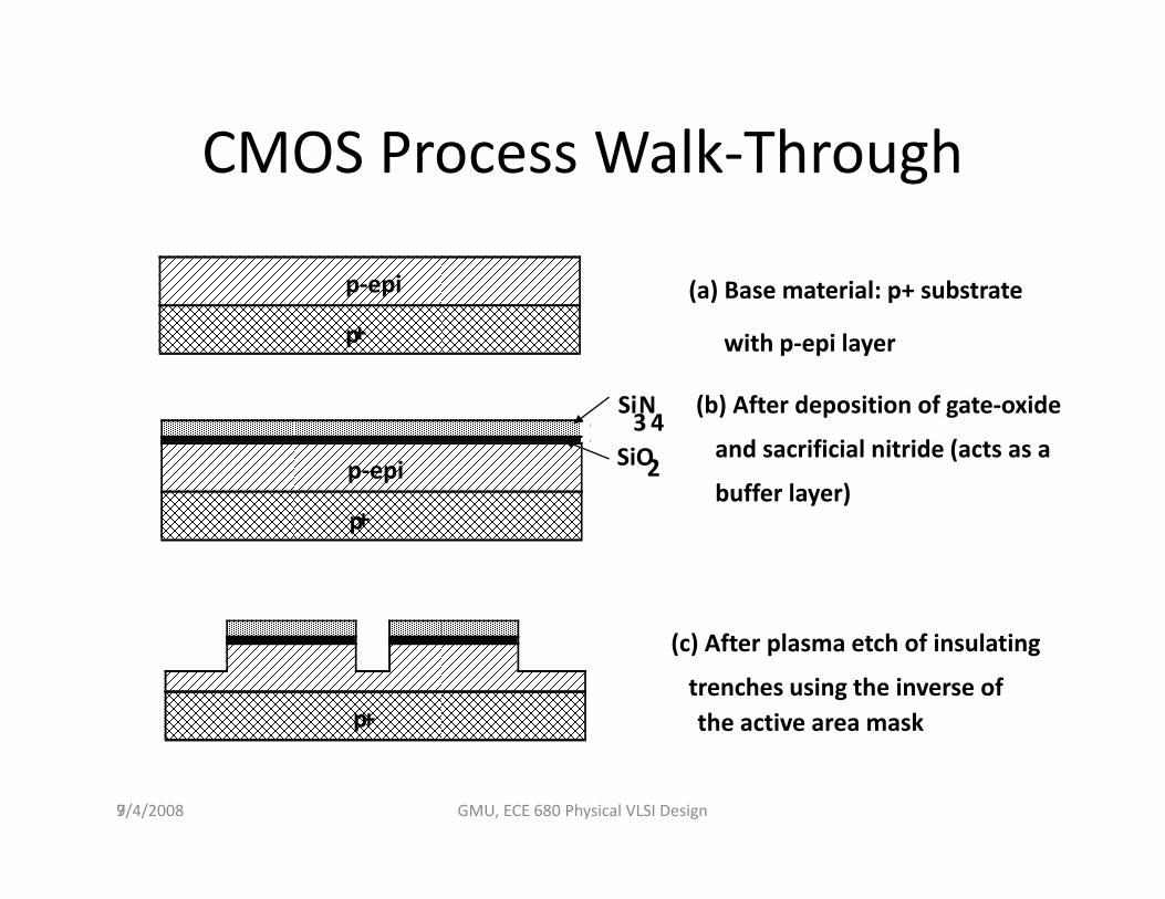
CMOS Process Walk‐ThroughCMOS Process Walk Through
p epi
p+
p‐epi (a) Base material: p+ substrate
with p‐epi layer
p‐epi SiO2
3SiN
4(b) After deposition of gate‐oxide
and sacrificial nitride (acts as a
buffer layer)p+
p+
(c) After plasma etch of insulating
trenches using the inverse of the active area mask
79/4/2008 GMU, ECE 680 Physical VLSI Design

CMOS Process Walk‐ThroughCMOS Process Walk ThroughSiO2 (d) After trench filling, CMP
planarization, and removal ofplanarization, and removal of sacrificial nitride
(e) After n‐well and
V adjust implantsn
VTp adjust implants
(f) After p‐well and
VTn adjust implantsp
89/4/2008 GMU, ECE 680 Physical VLSI Design

CMOS Process Walk‐ThroughCMOS Process Walk Throughpoly(silicon)
(g) After Poly‐Si deposition(g) After Poly‐Si depositionand etch
p+n+ (h) After n+ source/drain and P+ source/drain implants. At the same time these step also dope the
SiO2
these step also dope the Poly‐Si
2(i) After deposition of SiO2 Insulator and contact hole etch
99/4/2008 GMU, ECE 680 Physical VLSI Design

CMOS Process Walk‐ThroughCMOS Process Walk Through
Al
(j) After deposition and
patterning of first Al layer.
Al
M3
(k) After deposition of SiOinsulator etching of via’s
AlSiO2
M2
M3
insulator, etching of via s,deposition and patterning ofsecond layer of Al.
M1
109/4/2008 GMU, ECE 680 Physical VLSI Design

Advanced Metallization
11 SEM image of a real circuit whose oxide was etched9/4/2008 GMU, ECE 680 Physical VLSI Design

Design RulesDesign Rules
129/4/2008 GMU, ECE 680 Physical VLSI Design
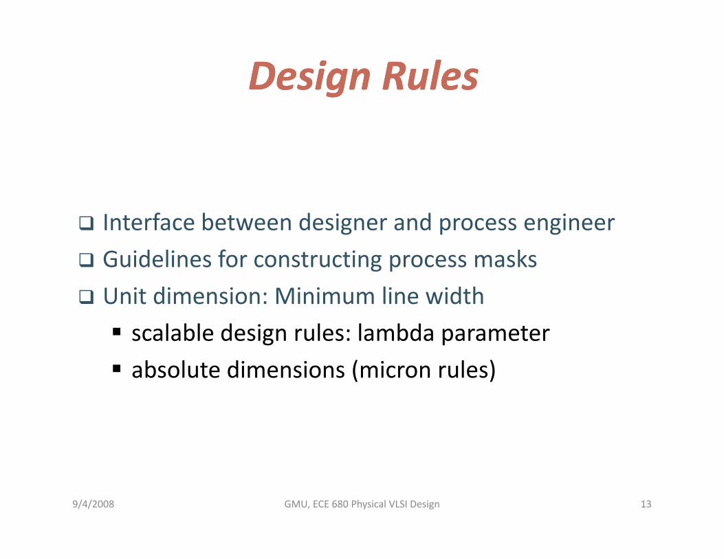
Design RulesDesign Rules
Interface between designer and process engineer
Guidelines for constructing process masks
Unit dimension: Minimum line width
scalable design rules: lambda parameter
absolute dimensions (micron rules)
139/4/2008 GMU, ECE 680 Physical VLSI Design
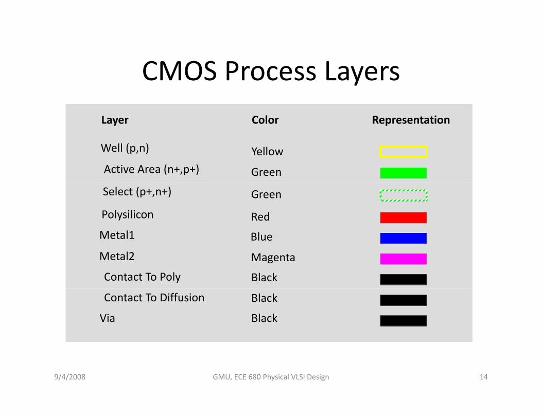
CMOS Process LayersCMOS Process Layers
Layer Color Representation
Well (p,n)
Active Area (n+,p+)
Yellow
Green
Polysilicon
Metal1
Red
Blue
Select (p+,n+) Green
Metal1
Metal2
Contact To Poly
Blue
Magenta
Black
Contact To Diffusion
Via
Black
Black
9/4/2008 14GMU, ECE 680 Physical VLSI Design
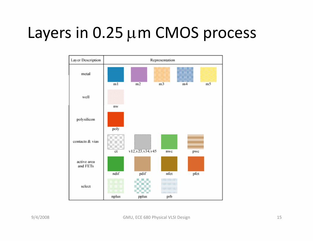
Layers in 0.25 μm CMOS process
9/4/2008 15GMU, ECE 680 Physical VLSI Design

Intra‐Layer Design RulesIntra Layer Design RulesDifferent PotentialSame Potential
10
90
Well Polysilicon2
2
or6
10
Active3
2
Metal1 3
Contact
Metal24
3 32
Co cor Via
Select2
2Hole
3
Select
9/4/2008 16GMU, ECE 680 Physical VLSI Design

Transistor Layout
1
Tran
sist
or
23
T
2
5
9/4/2008 17GMU, ECE 680 Physical VLSI Design
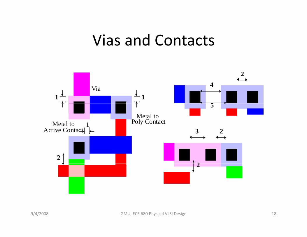
Vias and ContactsVias and Contacts
2
1Via
1
2
5
4
1Metal to
Poly ContactMetal toActive Contact
5
3 2
222
9/4/2008 18GMU, ECE 680 Physical VLSI Design
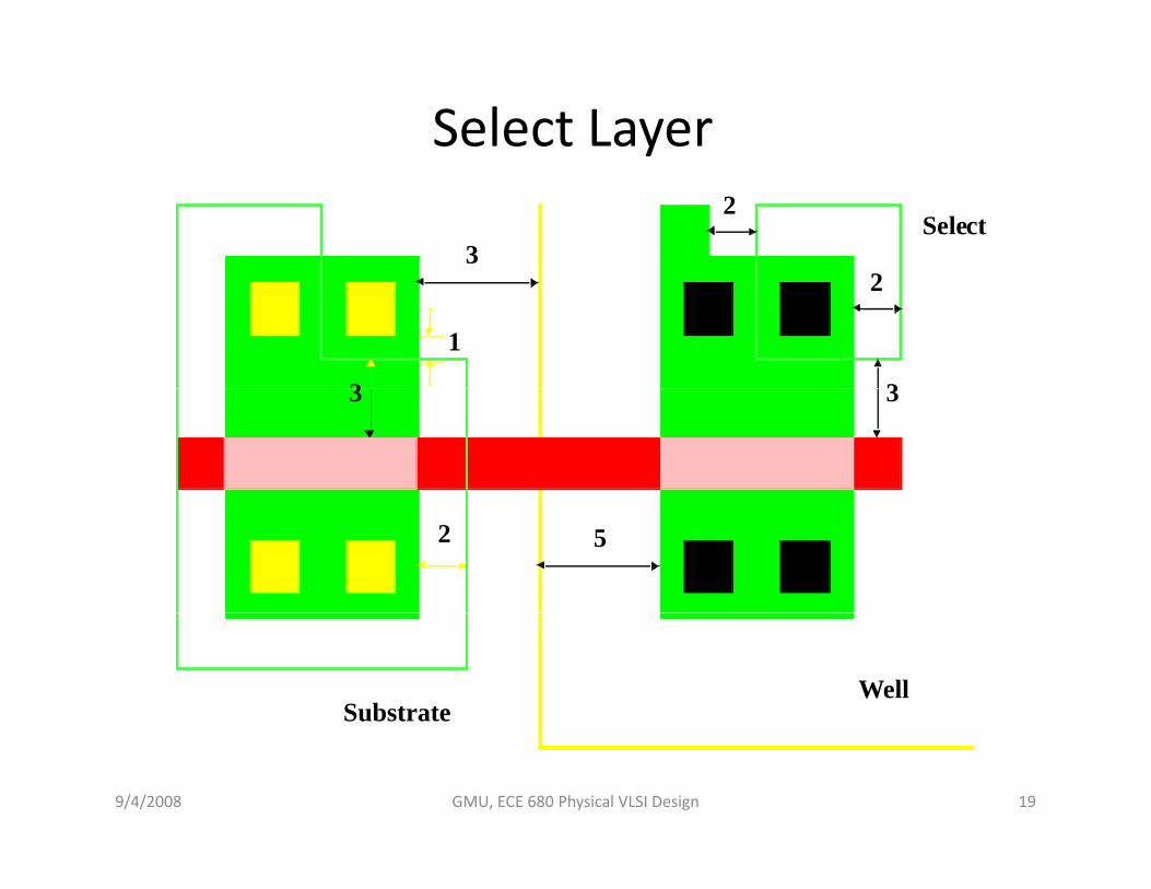
Select Layer2
2
Select3
1
3 3
2
3 3
2 5
WellSubstrate
9/4/2008 19GMU, ECE 680 Physical VLSI Design

CMOS Inverter LayoutCMOS Inverter LayoutInGND VDD
A A’
Out
(a) Layout
np-substrate Field
Oxidep+n+
A A’
(b) Cross-Section along A-A’
9/4/2008 20GMU, ECE 680 Physical VLSI Design

Layout EditorLayout Editor
9/4/2008 21GMU, ECE 680 Physical VLSI Design

PackagingPackaging
El t i l L iti• Electrical: Low parasitics
• Mechanical: Reliable and robust
• Thermal: Efficient heat removal
• Economical: CheapEconomical: Cheap
9/4/2008 22GMU, ECE 680 Physical VLSI Design

Bonding Techniques
Wire Bonding
SubstrateSubstrate
Die
Pad
Lead Frame
9/4/2008 23GMU, ECE 680 Physical VLSI Design

Package Types
9/4/2008 24GMU, ECE 680 Physical VLSI Design

Package Parameters
9/4/2008 25GMU, ECE 680 Physical VLSI Design
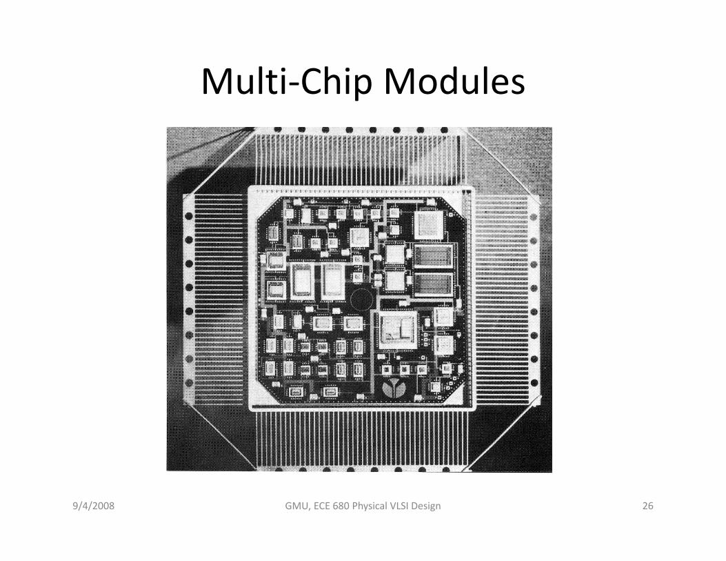
Multi‐Chip Modules
9/4/2008 26GMU, ECE 680 Physical VLSI Design