eec 116 lecture #1: course overview - uc davis eceramirtha/eec116/f11/lecture1.pdf · eec 116...
TRANSCRIPT

EEC 116 Lecture #1:Course Overview
Rajeevan Amirtharajah Bevan Baas
University of California, DavisJeff Parkhurst
Intel Corporation
Amirtharajah, EEC 116 Fall 2011 2
Permissions to Use Conditions & Acknowledgment
• Permission is granted to copy and distribute this slide set for educational purposes only, provided that the complete bibliographic citation and following credit line is included: "Copyright 2002 J. Rabaey et al." Permission is granted to alter and distribute this material provided that the following credit line is included: "Adapted from (complete bibliographic citation). Copyright 2002 J. Rabaey et al."This material may not be copied or distributed for commercial purposes without express written permission of the copyright holders.
• Slides 13-17 Adapted from CSE477 VLSI Digital Circuits Lecture Slides by Vijay Narayanan and Mary Jane Irwin, Penn State University
Amirtharajah, EEC 116 Fall 2011 3
Outline
• Administrative Details
• Survey of Digital IC Technology
• MOS Fabrication
• Layout Overview
• MOSFET Overview
Amirtharajah, EEC 116 Fall 2011 4
Personnel
• Prof. Raj Amirtharajah (Instructor)Office: 3173 Kemper HallEmail: [email protected] put EEC 116 in email subject line.Office Hours: F 2 - 3 PM or by appointment.
• Stanley HsuEmail: [email protected] Hours: Tu 2-4 2107 Kemper
• LabsWednesdays 6 PM – 9 PM 2107 Kemper
Amirtharajah, EEC 116 Fall 2011 5
Course Materials
• TextbookDigital Integrated Circuits (2nd ed.) by J. Rabaey, A. Chandrakasan, and B. Nikolic
• Suggested ReferencesCMOS Digital Integrated Circuits (3rd ed.) Kang and LeblebiciCMOS VLSI Design (4th ed.) Weste, Harris (or earlier editions)
• HandoutsLabs, lab report cover sheets, slides, and lecture notes available
on course web page in PDF format.• Web Page
http://www.ece.ucdavis.edu/~ramirtha/EEC116/F11/F11.htmlLinked from SmartSite

Amirtharajah, EEC 116 Fall 2011 6
Grading
• Letter
• A: 100 - 90%
• B: 90 - 80%• C: 80 - 70%• D: 70 - 60%• F: below 60%
• Expect class average to be around B- / C+• Curving will only help you

Amirtharajah, EEC 116 Fall 2011 7
Weighting
• Labs 35%• Weekly Homework 5%
Scale for each problem: 0 = poor effort, 1 = close, but fundamental problem, 2 = correct
• Quizzes 10%Four throughout the quarter (approx. every other week),
lowest score dropped (April 11, April 25, May 18, May 25)• Midterm 20%
Monday, October 31, in class• Final 30%
Wednesday, December 7, 1:00 - 3:00 PMCumulative, but emphasizes material after midterm

Amirtharajah, EEC 116 Fall 2011 8
Colored Pencils
• Buy colored pencils or pens whose colors match Cadence layout tool layer colors
– green
– brown (orange next closest?)
– red
– blue
– purple
• Used for “stick diagrams”
• Slightly transparent pencils or pens work best
Amirtharajah, EEC 116 Fall 2011 9
Labs and CAD Software Usage
• Need to know/learn Cadence/Spectre – Circuit Simulation
• Can work on labs remotely using VNC, etc.

Amirtharajah, EEC 116 Fall 2011 10
Moore’s Law

Amirtharajah, EEC 116 Fall 2011 11
Advances in Memory Density
Source: Digital Integrated Circuits, 2nd ©
Amirtharajah, EEC 116 Fall 2011 12
Hybrid to Monolithic Trend
• We continue to integrate multiple functions on a single chip– Mixture of Analog, Radio Frequency (RF), Digital
– Graphics/Motherboard chipset an example of this
• Cost and Performance driving market– Higher performance achieved on chip than off chip
– Lower cost due to a single die versus multi-chip design
– Saves on packaging, total area by eliminating redundant functions
• System-on-a-Chip (SOC) concept
Amirtharajah, EEC 116 Fall 2011 13
Education Demand for Circuit Design• Industry needs circuit designers
– Not just logic designers• Must understand operation at transistor level
– Not just digital designers• Must understand analog effects
– Not just analog designers• Must be able to comprehend Deep Sub-Micron
(DSM) effects (<0.13um)• Fundamental circuit knowledge critical
– Similar techniques for bipolar transistors, NMOS (even relays and vacuum tubes!)
– Must be able to exploit nanoscale devices in future
Amirtharajah, EEC 116 Fall 2011 14
Education Demand for System Design• Industry needs system designers
– Need to understand system implications of your design
• Power Delivery, Clock Loading – What do you need– Need to design from the system point of view
• Communication protocol – how to effectively talk with other blocks
• What should be added into your block to meet system design requirements(i.e. comprehend soft block methodology for optimization of area, interconnect, etc.)
You must operate at both levels!
Amirtharajah, EEC 116 Fall 2011 15
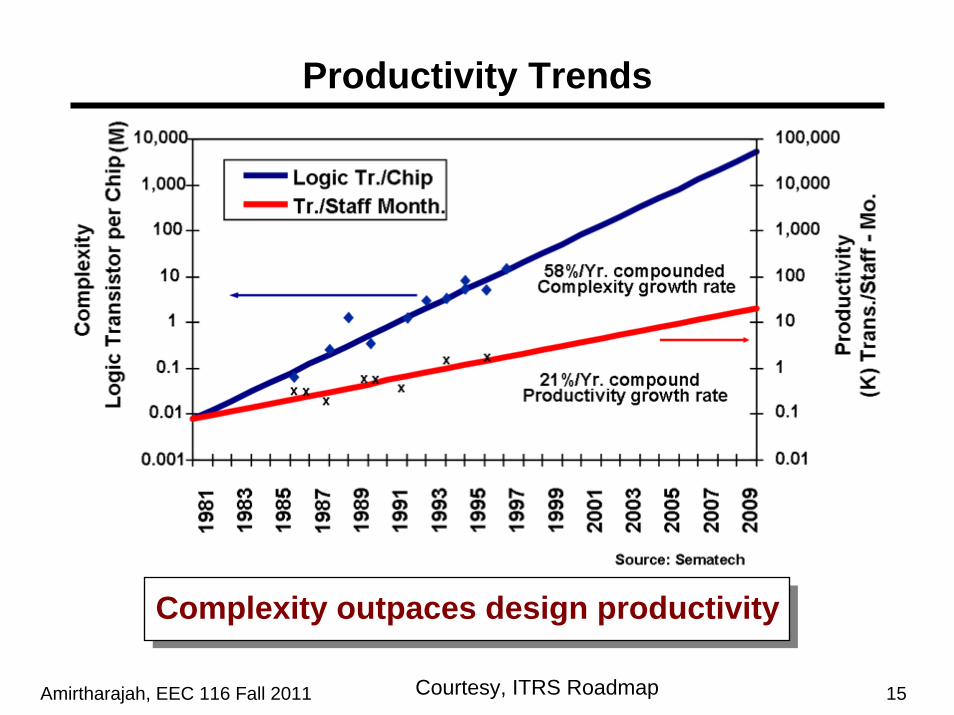
Productivity Trends
Complexity outpaces design productivity
Courtesy, ITRS Roadmap
Amirtharajah, EEC 116 Fall 2011 16
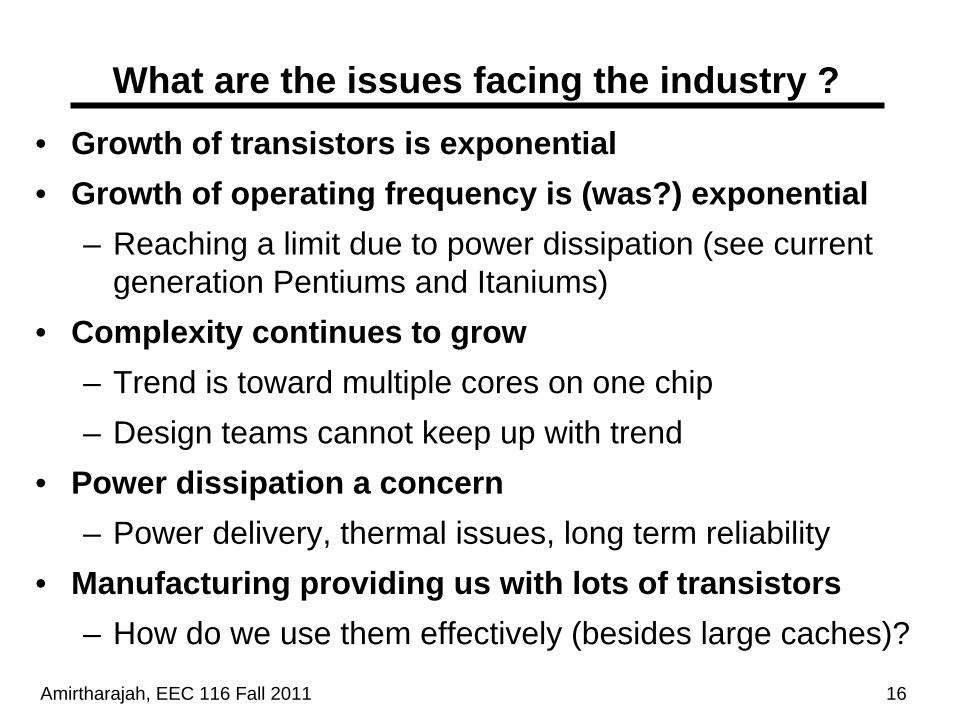
What are the issues facing the industry ?• Growth of transistors is exponential• Growth of operating frequency is (was?) exponential
– Reaching a limit due to power dissipation (see current generation Pentiums and Itaniums)
• Complexity continues to grow– Trend is toward multiple cores on one chip– Design teams cannot keep up with trend
• Power dissipation a concern– Power delivery, thermal issues, long term reliability
• Manufacturing providing us with lots of transistors– How do we use them effectively (besides large caches)?
Amirtharajah, EEC 116 Fall 2011 17
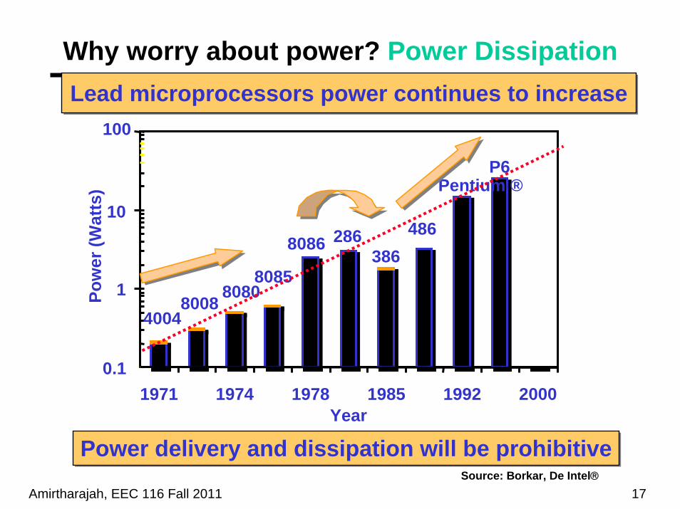
Why worry about power? Power Dissipation
P6Pentium ®
486386
2868086
808580808008
4004
0.1
1
10
100
1971 1974 1978 1985 1992 2000Year
Pow
er (W
atts
)Lead microprocessors power continues to increaseLead microprocessors power continues to increase
Power delivery and dissipation will be prohibitivePower delivery and dissipation will be prohibitiveSource: Borkar, De Intel®
Amirtharajah, EEC 116 Fall 2011 18
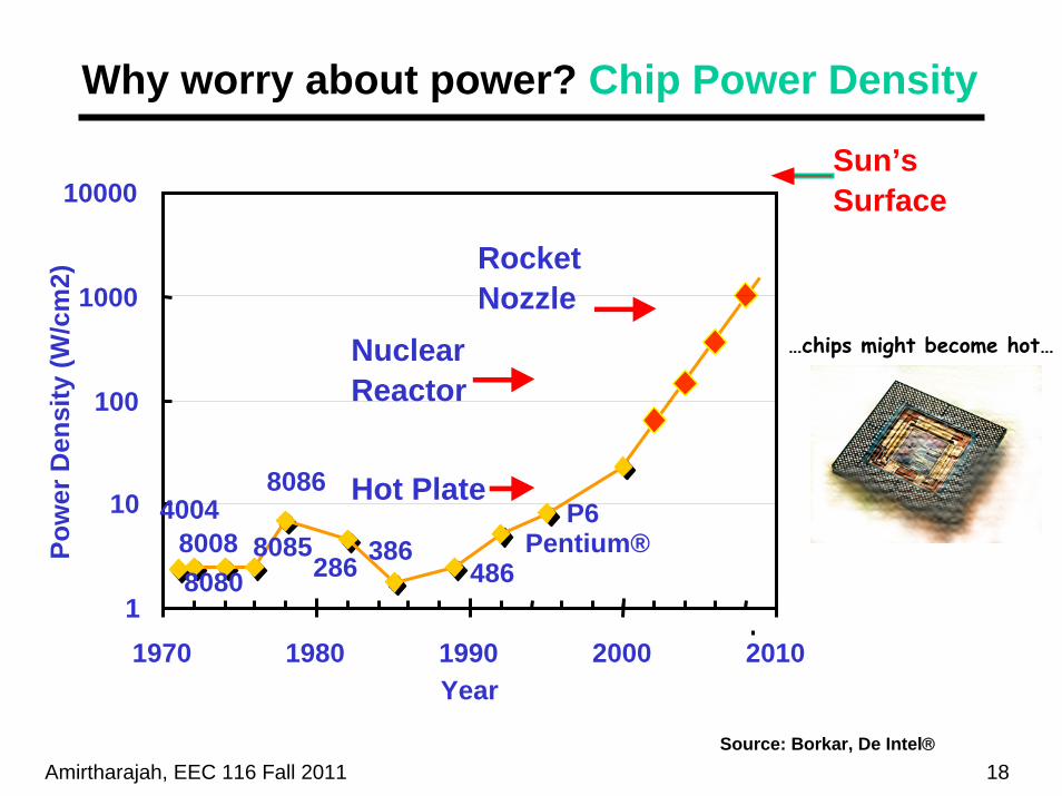
Why worry about power? Chip Power Density
400480088080
8085
8086
286 386486
Pentium®P6
1
10
100
1000
10000
1970 1980 1990 2000 2010Year
Pow
er D
ensi
ty (W
/cm
2)
Hot Plate
NuclearReactor
RocketNozzle
Sun’sSurface
…chips might become hot…
Source: Borkar, De Intel®
Amirtharajah, EEC 116 Fall 2011 19
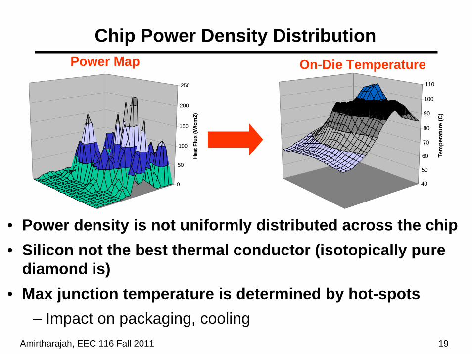
Chip Power Density Distribution
• Power density is not uniformly distributed across the chip• Silicon not the best thermal conductor (isotopically pure
diamond is)• Max junction temperature is determined by hot-spots
– Impact on packaging, cooling
0
50
100
150
200
250
Heat
Flu
x (W
/cm
2)
Power Map
40
50
60
70
80
90
100
110
Tem
pera
ture
(C)
On-Die Temperature
Amirtharajah, EEC 116 Fall 2011 20
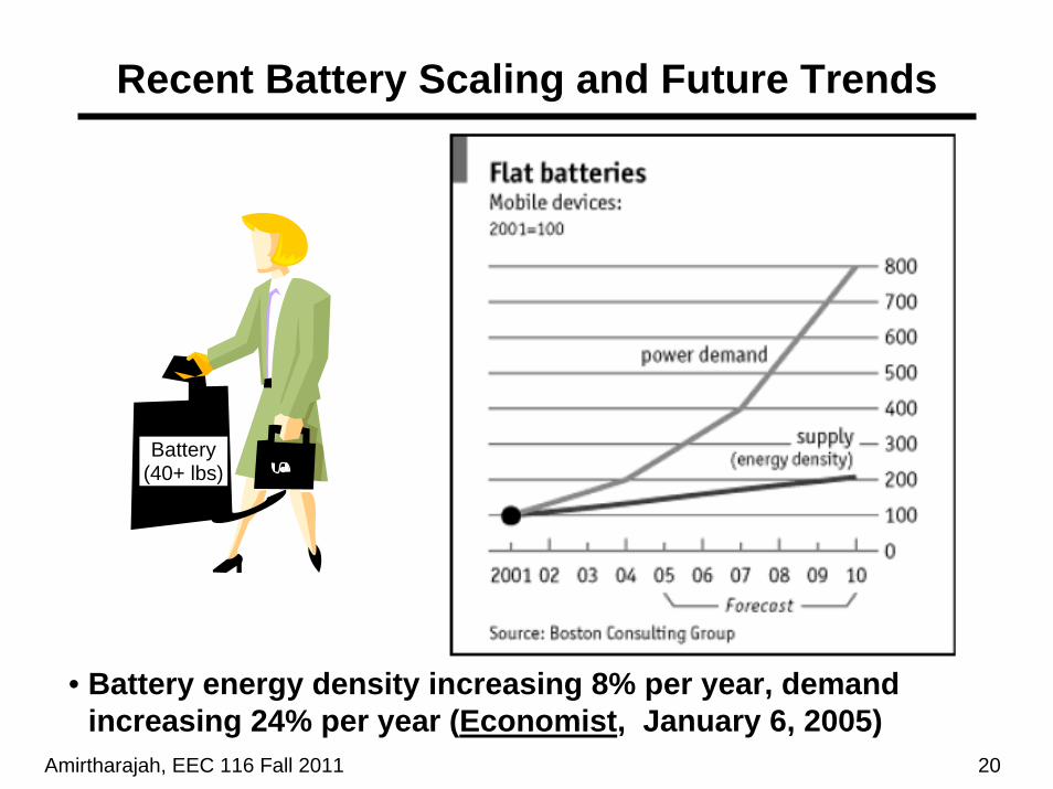
Recent Battery Scaling and Future Trends
• Battery energy density increasing 8% per year, demand increasing 24% per year (Economist, January 6, 2005)
Battery(40+ lbs)
Amirtharajah, EEC 116 Fall 2011 21
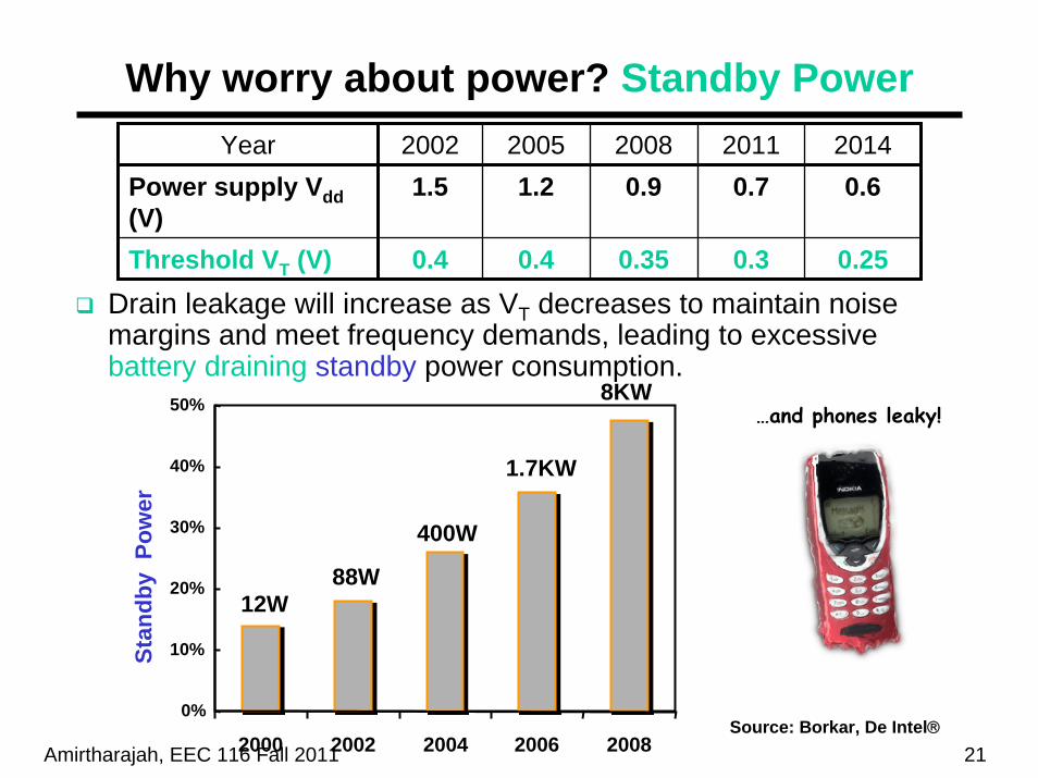
Why worry about power? Standby Power
Drain leakage will increase as VT decreases to maintain noise margins and meet frequency demands, leading to excessive battery draining standby power consumption.
8KW
1.7KW
400W
88W 12W
0%
10%
20%
30%
40%
50%
2000 2002 2004 2006 2008
Stan
dby
Pow
er
Source: Borkar, De Intel®
Year 2002 2005 2008 2011 2014Power supply Vdd(V)
1.5 1.2 0.9 0.7 0.6
Threshold VT (V) 0.4 0.4 0.35 0.3 0.25
…and phones leaky!
Amirtharajah, EEC 116 Fall 2011 22
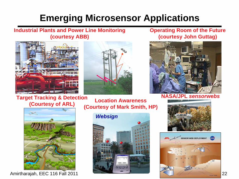
Industrial Plants and Power Line Monitoring(courtesy ABB)
Operating Room of the Future(courtesy John Guttag)
Target Tracking & Detection(Courtesy of ARL) Location Awareness
(Courtesy of Mark Smith, HP)
Websign
NASA/JPL sensorwebs
Emerging Microsensor Applications
Amirtharajah, EEC 116 Fall 2011 23
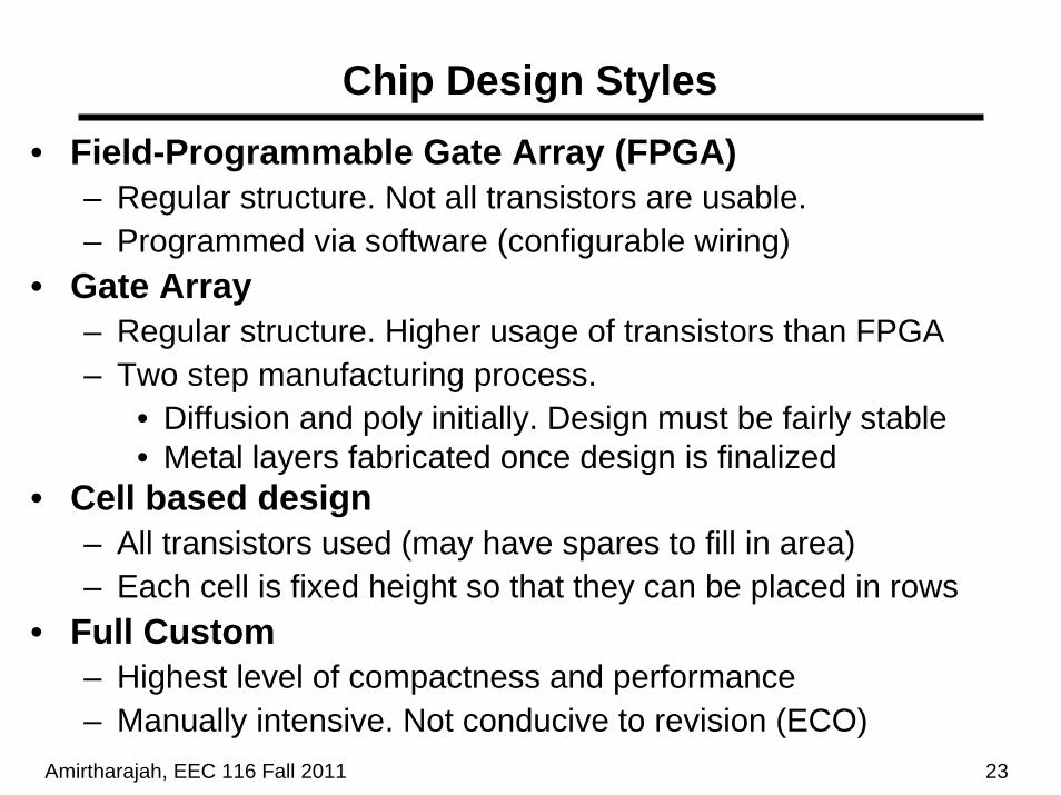
Chip Design Styles• Field-Programmable Gate Array (FPGA)
– Regular structure. Not all transistors are usable.– Programmed via software (configurable wiring)
• Gate Array– Regular structure. Higher usage of transistors than FPGA– Two step manufacturing process.
• Diffusion and poly initially. Design must be fairly stable• Metal layers fabricated once design is finalized
• Cell based design– All transistors used (may have spares to fill in area)– Each cell is fixed height so that they can be placed in rows
• Full Custom– Highest level of compactness and performance– Manually intensive. Not conducive to revision (ECO)
Amirtharajah, EEC 116 Fall 2011 24
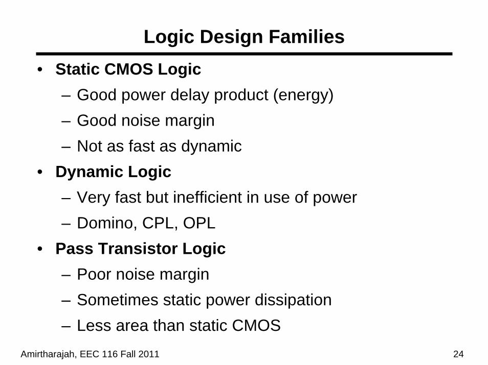
Logic Design Families• Static CMOS Logic
– Good power delay product (energy)– Good noise margin– Not as fast as dynamic
• Dynamic Logic– Very fast but inefficient in use of power– Domino, CPL, OPL
• Pass Transistor Logic– Poor noise margin– Sometimes static power dissipation– Less area than static CMOS
Amirtharajah, EEC 116 Fall 2011 25
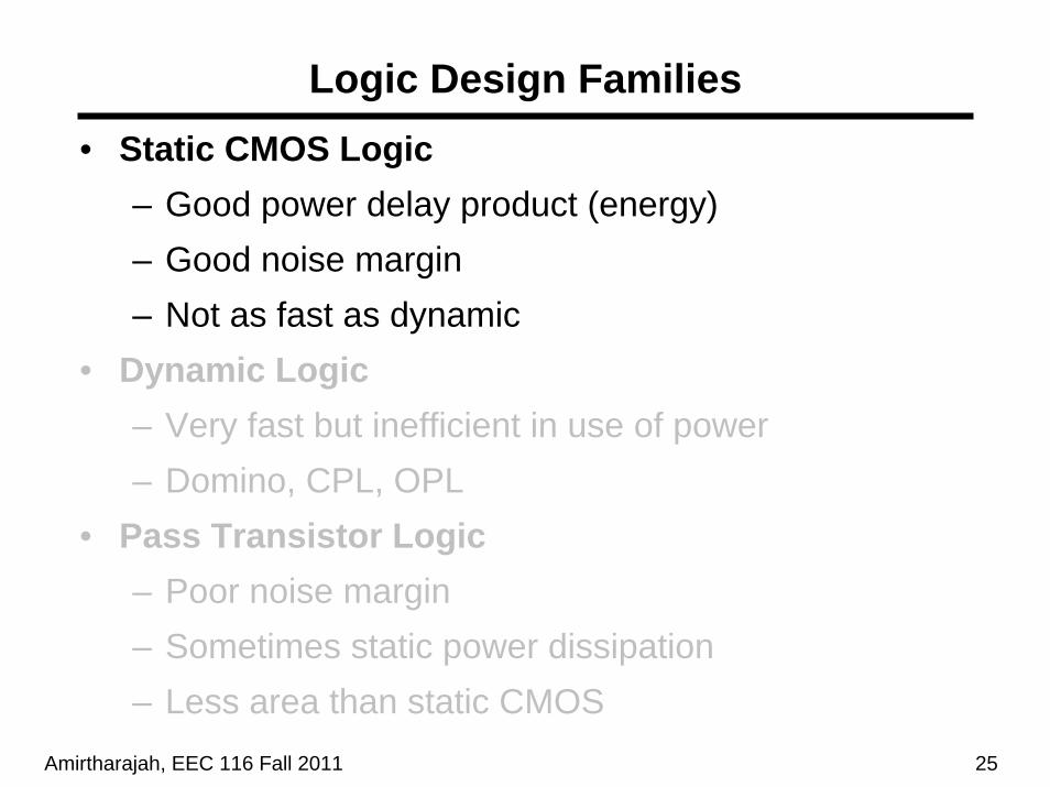
Logic Design Families• Static CMOS Logic
– Good power delay product (energy)– Good noise margin– Not as fast as dynamic
• Dynamic Logic– Very fast but inefficient in use of power– Domino, CPL, OPL
• Pass Transistor Logic– Poor noise margin– Sometimes static power dissipation– Less area than static CMOS

Amirtharajah, EEC 116 Fall 2011 26
Design Parameters
• Reliability (Dealt with when relating to layout)
– Factors that dictate reliable operation of the circuit• Electromigration, thermal issues, hot electrons,
noise margins
• Performance (Not dealt with in this class)
– Not just measured in clock speed. Power-Delay Product (PDP, equivalent to energy) is a better measure
• Area
– Directly affects cost
Amirtharajah, EEC 116 Fall 2011 27
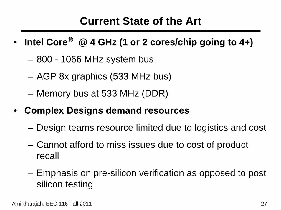
Current State of the Art
• Intel Core® @ 4 GHz (1 or 2 cores/chip going to 4+)
– 800 - 1066 MHz system bus
– AGP 8x graphics (533 MHz bus)
– Memory bus at 533 MHz (DDR)
• Complex Designs demand resources
– Design teams resource limited due to logistics and cost
– Cannot afford to miss issues due to cost of product recall
– Emphasis on pre-silicon verification as opposed to post silicon testing
Amirtharajah, EEC 116 Fall 2011 28
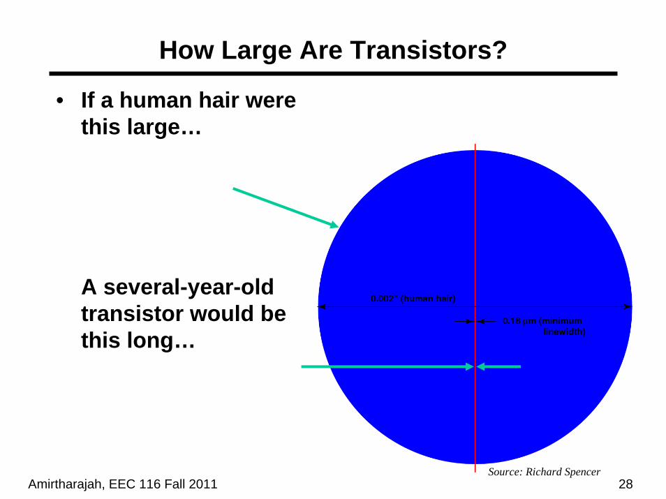
How Large Are Transistors?
• If a human hair were this large…
A several-year-old transistor would be this long…
Source: Richard Spencer
Amirtharajah, EEC 116 Fall 2011 29
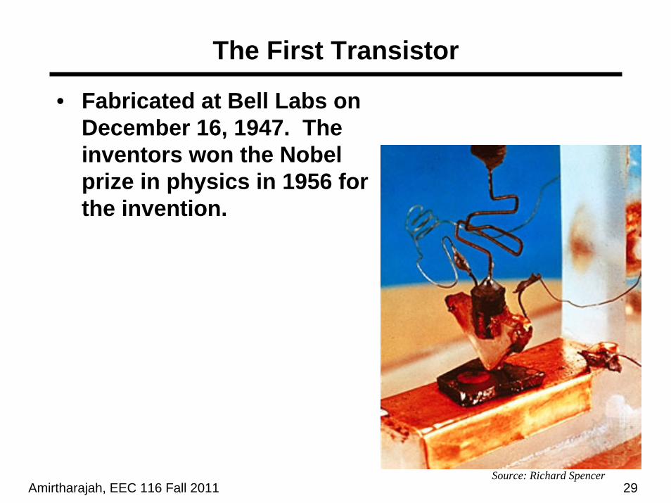
The First Transistor
• Fabricated at Bell Labs on December 16, 1947. The inventors won the Nobel prize in physics in 1956 for the invention.
Source: Richard Spencer
Amirtharajah, EEC 116 Fall 2011 30
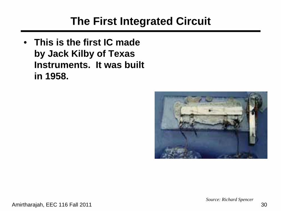
The First Integrated Circuit
• This is the first IC made by Jack Kilby of Texas Instruments. It was built in 1958.
Source: Richard Spencer
Amirtharajah, EEC 116 Fall 2011 31
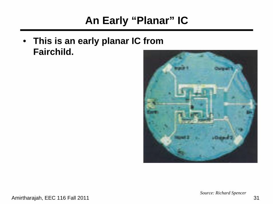
An Early “Planar” IC
• This is an early planar IC from Fairchild.
Source: Richard Spencer
Amirtharajah, EEC 116 Fall 2011 32
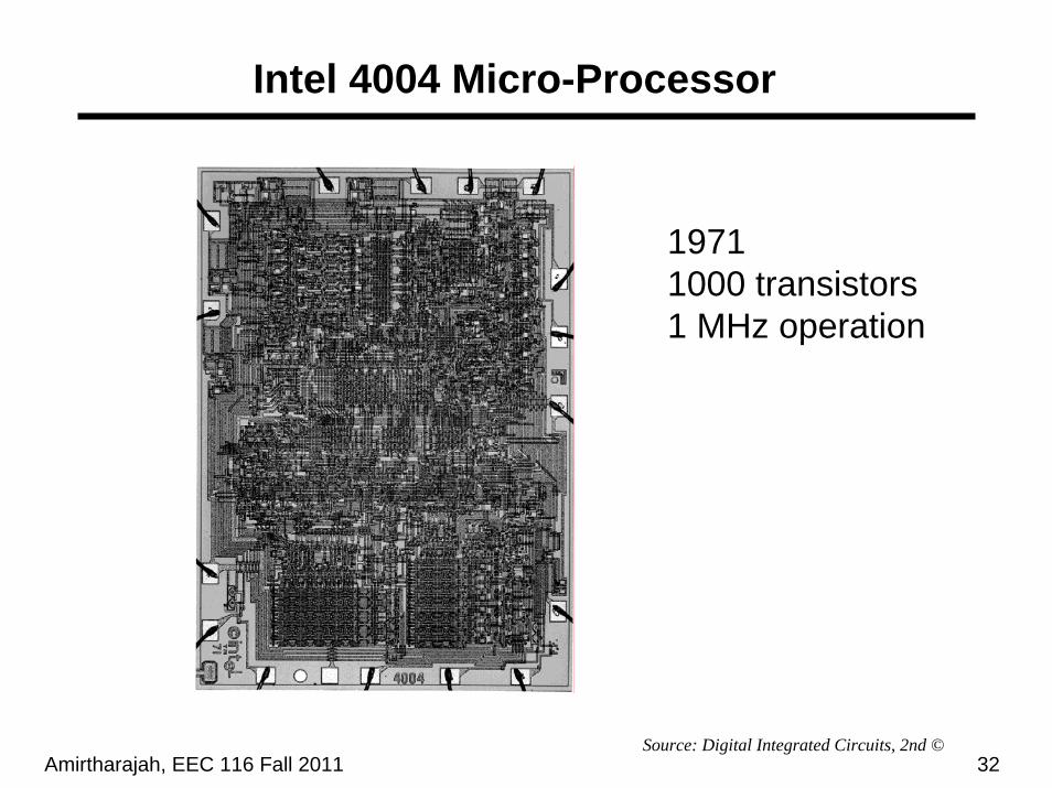
Intel 4004 Micro-Processor
19711000 transistors1 MHz operation
Source: Digital Integrated Circuits, 2nd ©
Amirtharajah, EEC 116 Fall 2011 33
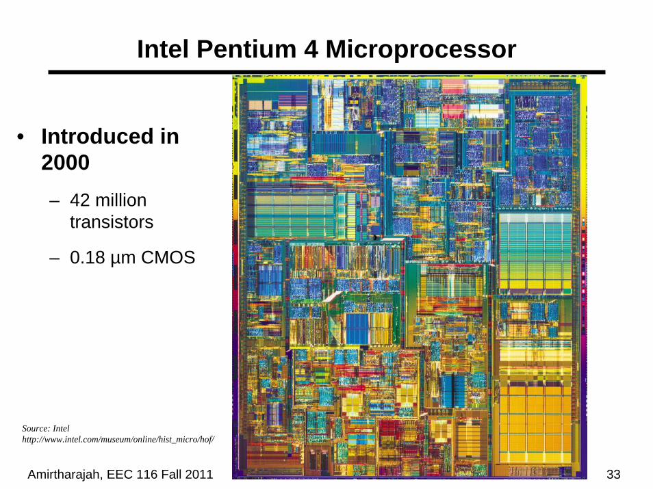
• Introduced in 2000– 42 million
transistors
– 0.18 µm CMOS
Source: Intelhttp://www.intel.com/museum/online/hist_micro/hof/
Intel Pentium 4 Microprocessor
Amirtharajah, EEC 116 Fall 201134
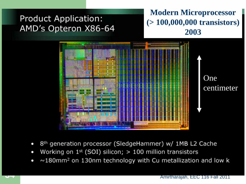
Onecentimeter
Modern Microprocessor(> 100,000,000 transistors)
2003
Amirtharajah, EEC 116 Fall 201135
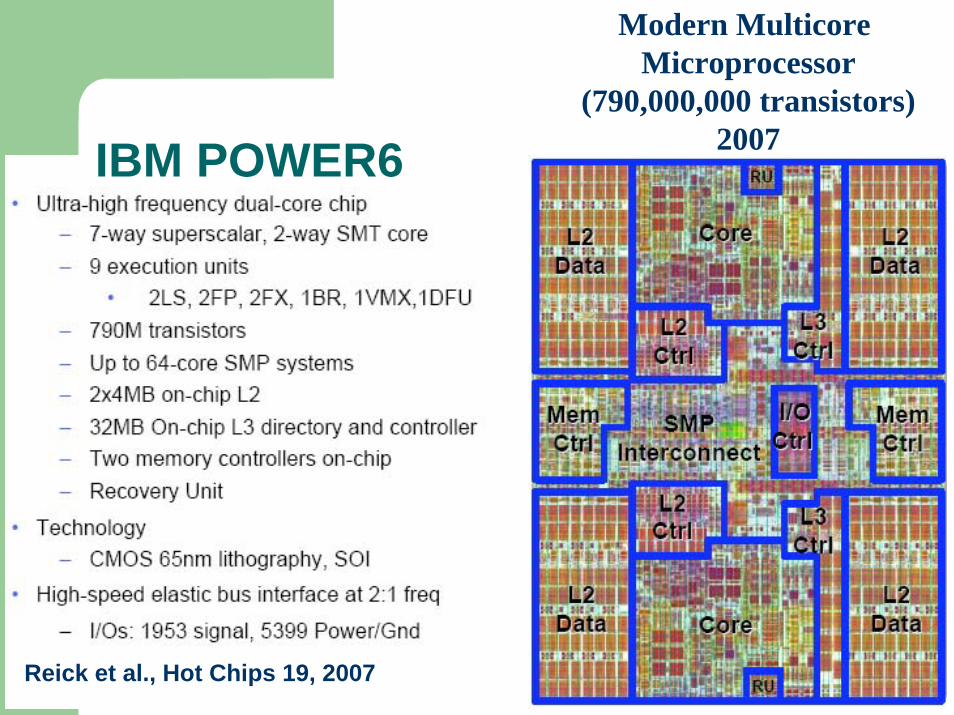
Modern MulticoreMicroprocessor
(790,000,000 transistors)2007IBM POWER6
Reick et al., Hot Chips 19, 2007

Amirtharajah, EEC 116 Fall 2011 36
• Introduced in 2010– 1.17 billion transistors, 32 nm CMOS
Source: Intel
Intel Westmere 6-Core Microprocessor
Amirtharajah, EEC 116 Fall 2011 37
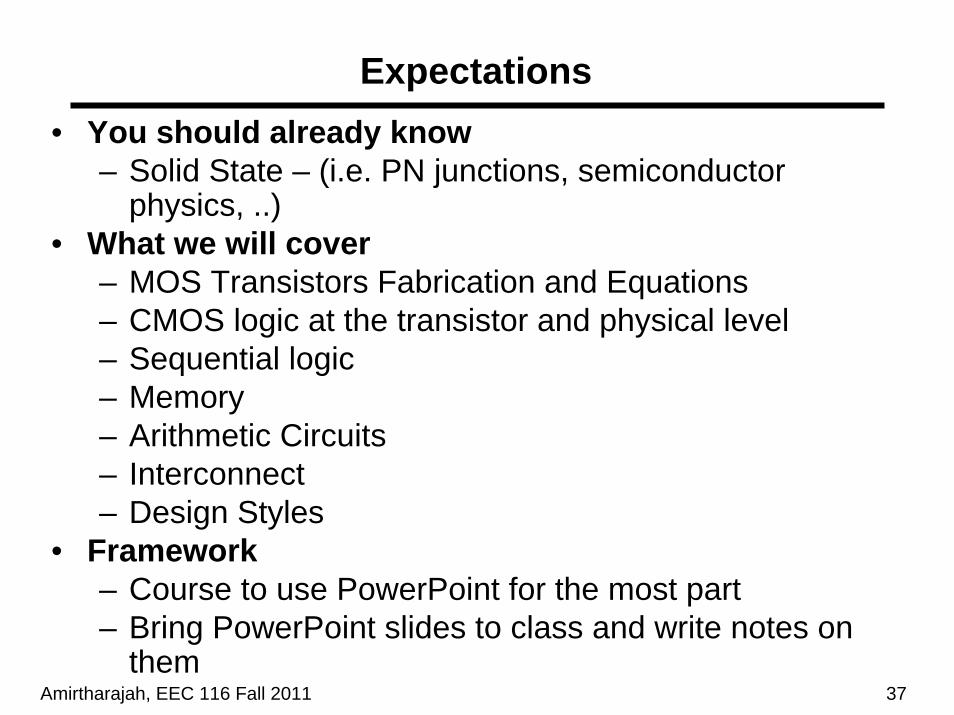
Expectations• You should already know
– Solid State – (i.e. PN junctions, semiconductor physics, ..)
• What we will cover– MOS Transistors Fabrication and Equations– CMOS logic at the transistor and physical level– Sequential logic– Memory– Arithmetic Circuits– Interconnect– Design Styles
• Framework– Course to use PowerPoint for the most part– Bring PowerPoint slides to class and write notes on
them
Amirtharajah, EEC 116 Fall 2011 38
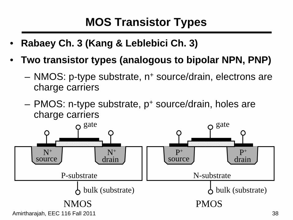
• Rabaey Ch. 3 (Kang & Leblebici Ch. 3)• Two transistor types (analogous to bipolar NPN, PNP)
– NMOS: p-type substrate, n+ source/drain, electrons are charge carriers
– PMOS: n-type substrate, p+ source/drain, holes are charge carriers
MOS Transistor Types
source drain
P-substrate
N+ N+
NMOS
source drain
N-substrate
P+ P+
PMOS
gate gate
bulk (substrate)bulk (substrate)
Amirtharajah, EEC 116 Fall 2011 39
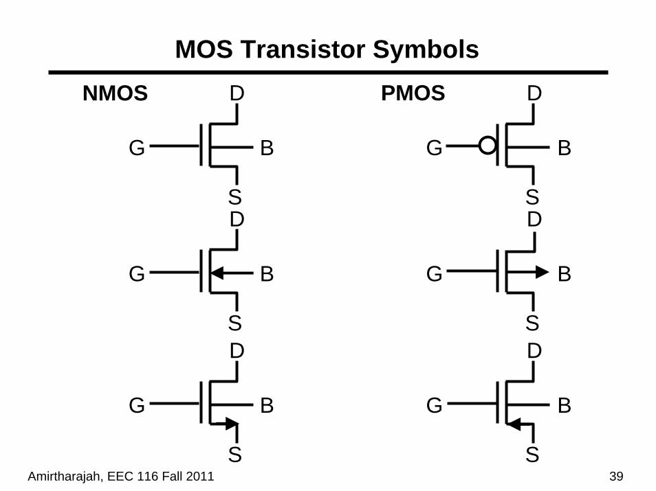
MOS Transistor SymbolsNMOS PMOSD
S
BG
D
S
BG
D
S
BG
D
S
BG
D
B
S
G
D
B
S
G
Amirtharajah, EEC 116 Fall 2011 40
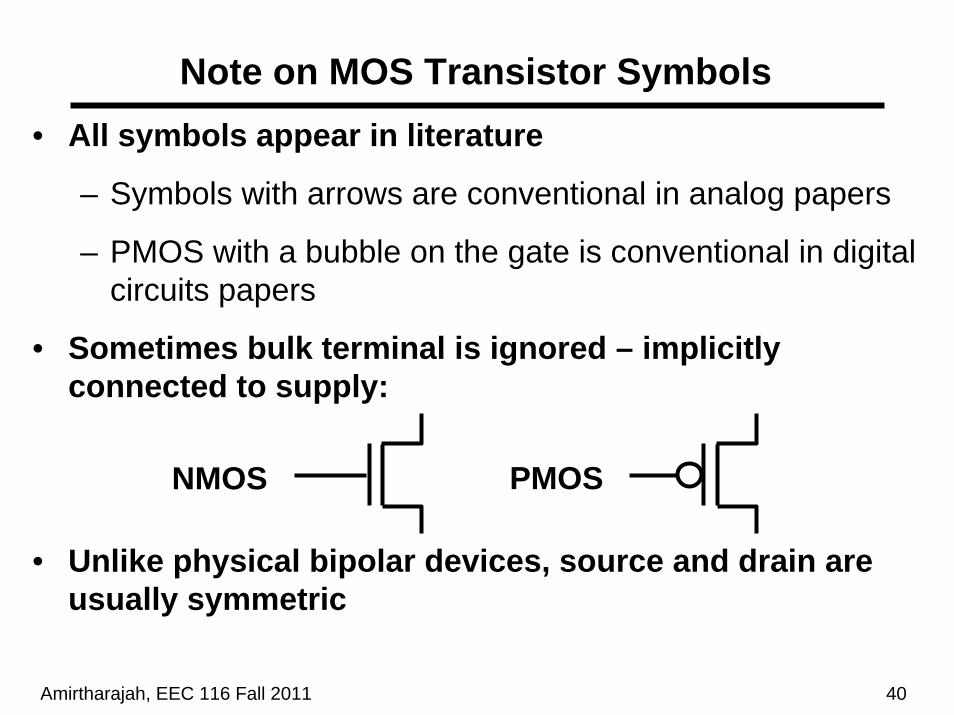
• All symbols appear in literature
– Symbols with arrows are conventional in analog papers
– PMOS with a bubble on the gate is conventional in digital circuits papers
• Sometimes bulk terminal is ignored – implicitly connected to supply:
• Unlike physical bipolar devices, source and drain are usually symmetric
Note on MOS Transistor Symbols
NMOS PMOS
Amirtharajah, EEC 116 Fall 2011 41
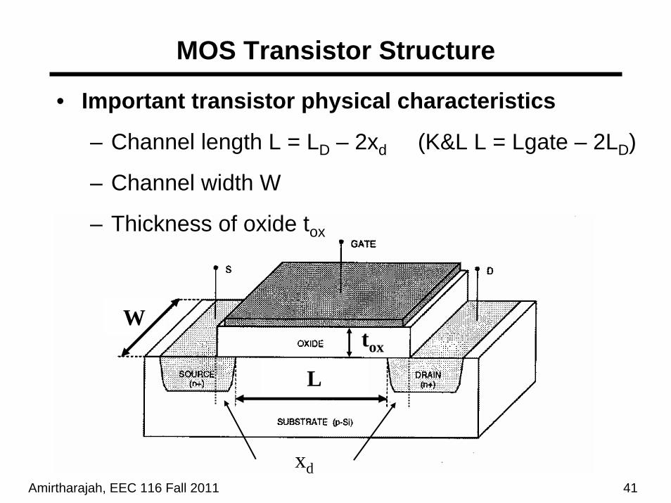
MOS Transistor Structure
L
Wtox
xd
• Important transistor physical characteristics
– Channel length L = LD – 2xd (K&L L = Lgate – 2LD)
– Channel width W
– Thickness of oxide tox
Amirtharajah, EEC 116 Fall 2011 42
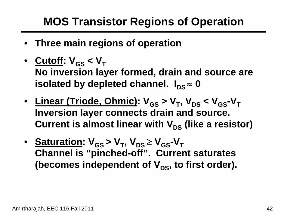
MOS Transistor Regions of Operation
• Three main regions of operation
• Cutoff: VGS < VTNo inversion layer formed, drain and source are isolated by depleted channel. IDS ≈ 0
• Linear (Triode, Ohmic): VGS > VT, VDS < VGS-VTInversion layer connects drain and source.Current is almost linear with VDS (like a resistor)
• Saturation: VGS > VT, VDS ≥ VGS-VTChannel is “pinched-off”. Current saturates (becomes independent of VDS, to first order).

Amirtharajah, EEC 116 Fall 2011 43
MOSFET Drain Current Overview
Linear (Triode, Ohmic):
“Classical” MOSFET model, will discuss deep submicron modifications as necessary (Rabaey, Eqs. 3.25, 3.29)
( ) ( )DSTGSox
D VVVL
WCI λμ+−= 1
22Saturation:
( ) ⎟⎟⎠
⎞⎜⎜⎝
⎛−−=
2
2DS
DSTGSoxDVVVV
LWCI μ
Cutoff: 0≈DI
Amirtharajah, EEC 116 Fall 2011 44
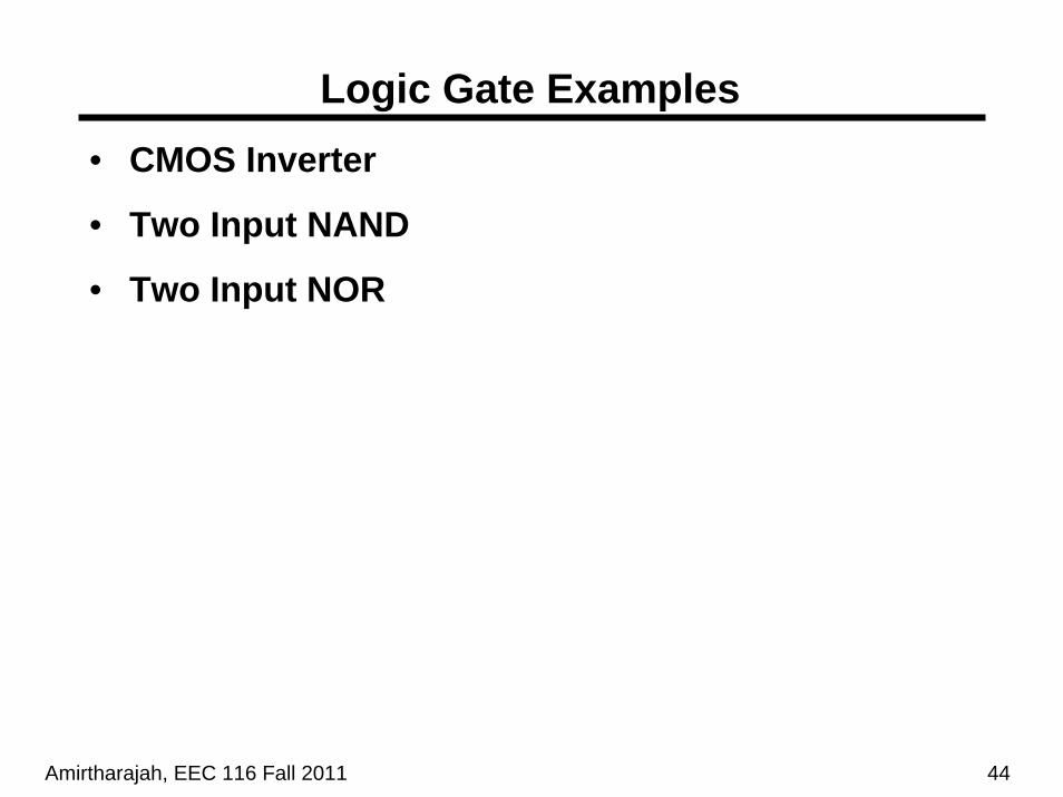
Logic Gate Examples• CMOS Inverter
• Two Input NAND
• Two Input NOR
Amirtharajah, EEC 116 Fall 2011 45
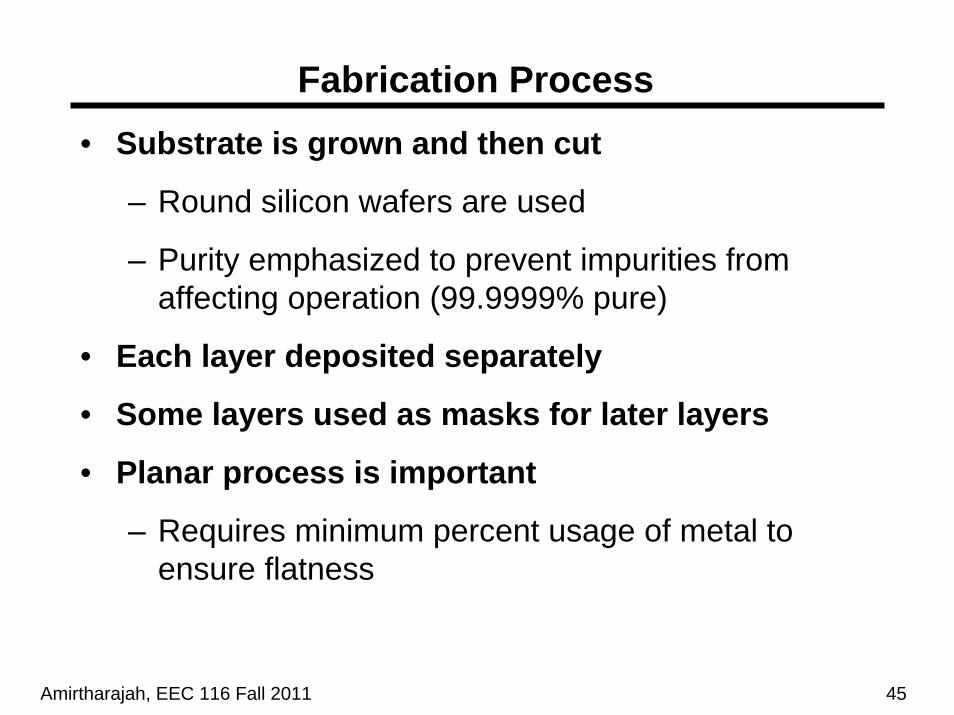
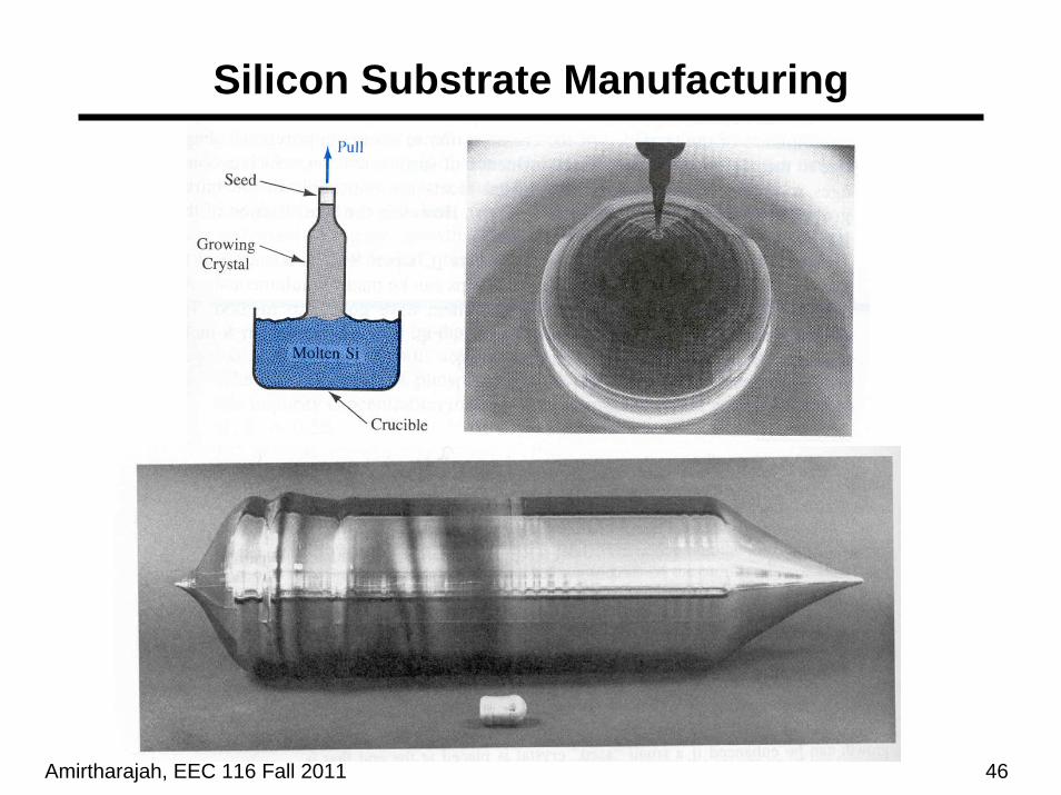
Fabrication Process• Substrate is grown and then cut
– Round silicon wafers are used
– Purity emphasized to prevent impurities from affecting operation (99.9999% pure)
• Each layer deposited separately
• Some layers used as masks for later layers
• Planar process is important
– Requires minimum percent usage of metal to ensure flatness
Amirtharajah, EEC 116 Fall 2011 46
Silicon Substrate Manufacturing
Amirtharajah, EEC 116 Fall 2011 47
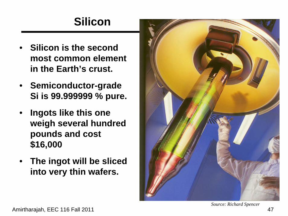
Silicon
• Silicon is the second most common element in the Earth’s crust.
• Semiconductor-grade Si is 99.999999 % pure.
• Ingots like this one weigh several hundred pounds and cost $16,000
• The ingot will be sliced into very thin wafers.
Source: Richard Spencer
Amirtharajah, EEC 116 Fall 2011 48
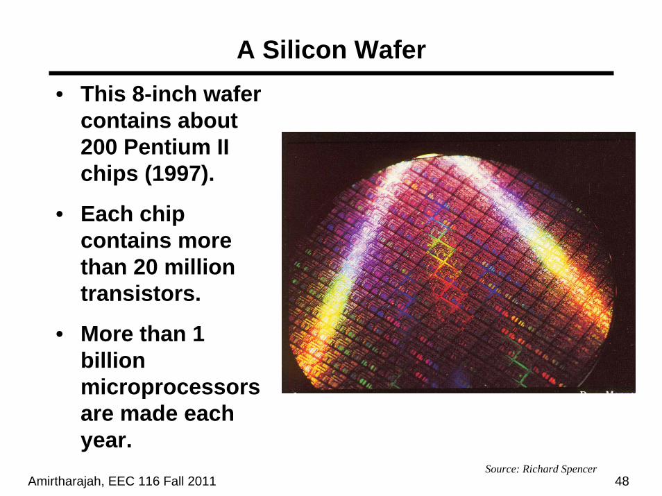
A Silicon Wafer• This 8-inch wafer
contains about 200 Pentium II chips (1997).
• Each chip contains more than 20 million transistors.
• More than 1 billion microprocessors are made each year.
Source: Richard Spencer
Amirtharajah, EEC 116 Fall 2011 49
A State-of-the-art Wafer
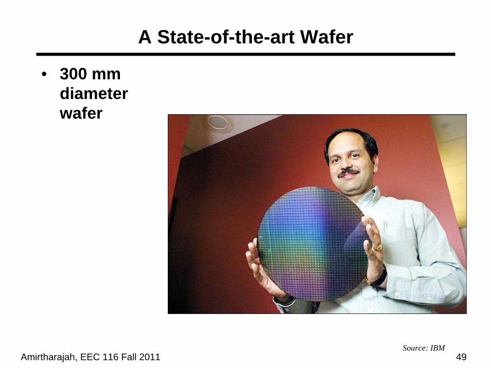
• 300 mm diameter wafer
Source: IBM

Amirtharajah, EEC 116 Fall 2011 50
Building a Golf Course with Similar Process
• Plane drops materials from the air– Sand, then dirt, then grass seeds, then trees– Certain masks applied during process to prevent material
from hitting particular areas– For instance: After Sand, mask placed over areas where
sand trap will exist. Mask later taken off at end of process to reveal sand trap.
Amirtharajah, EEC 116 Fall 2011 51
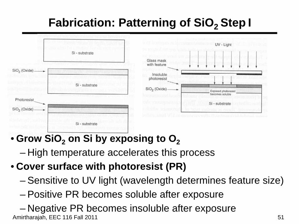
Fabrication: Patterning of SiO2 Step I
• Grow SiO2 on Si by exposing to O2– High temperature accelerates this process
• Cover surface with photoresist (PR)– Sensitive to UV light (wavelength determines feature size)– Positive PR becomes soluble after exposure– Negative PR becomes insoluble after exposure
Amirtharajah, EEC 116 Fall 2011 52
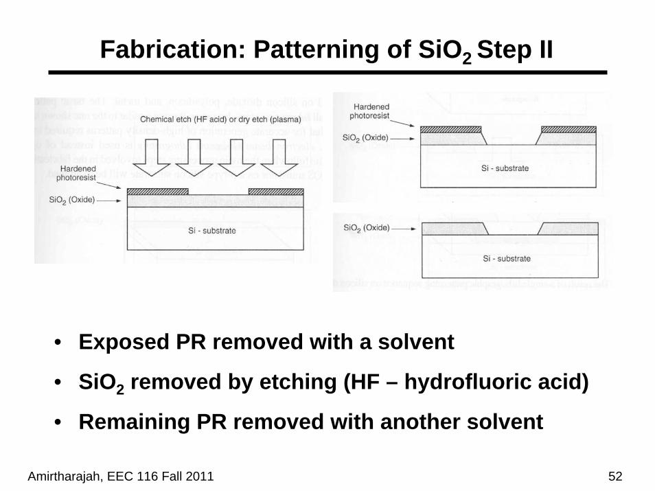
Fabrication: Patterning of SiO2 Step II
• Exposed PR removed with a solvent
• SiO2 removed by etching (HF – hydrofluoric acid)
• Remaining PR removed with another solvent

Amirtharajah, EEC 116 Fall 2011 53
NMOS Transistor Fabrication
• Thick field oxide grown
• Field oxide etched to create area for transistor
• Gate oxide (high quality) grown

Amirtharajah, EEC 116 Fall 2011 54
NMOS Transistor Fabrication
• Polysilicon deposited (doped to reduce resistance R)• Polysilicon etched to form gate• Gate oxide etched from source and drain
– Self-aligned process because source/drain aligned by gate
• Si doped with donors to create n+ regions
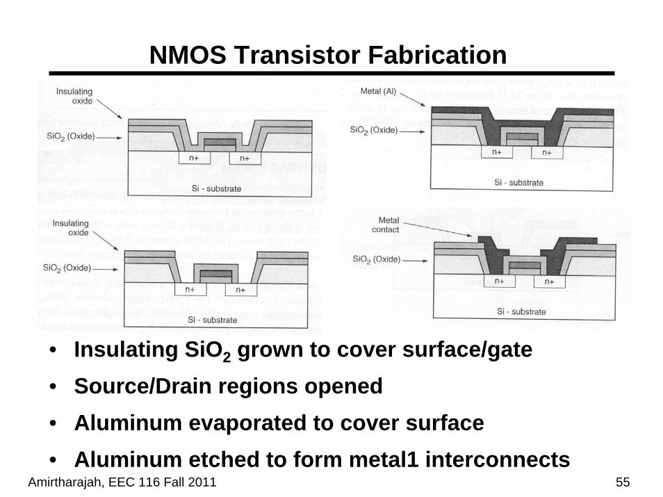
Amirtharajah, EEC 116 Fall 2011 55
NMOS Transistor Fabrication
• Insulating SiO2 grown to cover surface/gate• Source/Drain regions opened• Aluminum evaporated to cover surface• Aluminum etched to form metal1 interconnects
Amirtharajah, EEC 116 Fall 2011 56
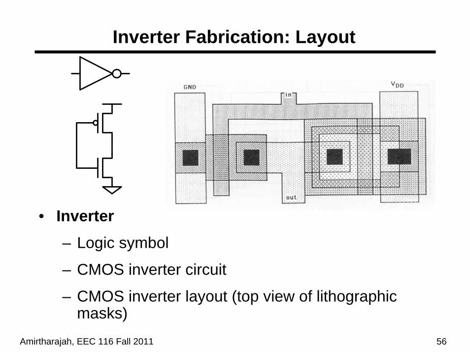
Inverter Fabrication: Layout
• Inverter– Logic symbol
– CMOS inverter circuit
– CMOS inverter layout (top view of lithographic masks)

Amirtharajah, EEC 116 Fall 2011 57
Inverter Fabrication: NWELL and Oxides
• N-wells created
• Thick field oxide grown surrounding active regions
• Thin gate oxide grown over active regions
Amirtharajah, EEC 116 Fall 2011 58
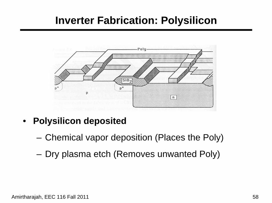
Inverter Fabrication: Polysilicon
• Polysilicon deposited
– Chemical vapor deposition (Places the Poly)
– Dry plasma etch (Removes unwanted Poly)
Amirtharajah, EEC 116 Fall 2011 59
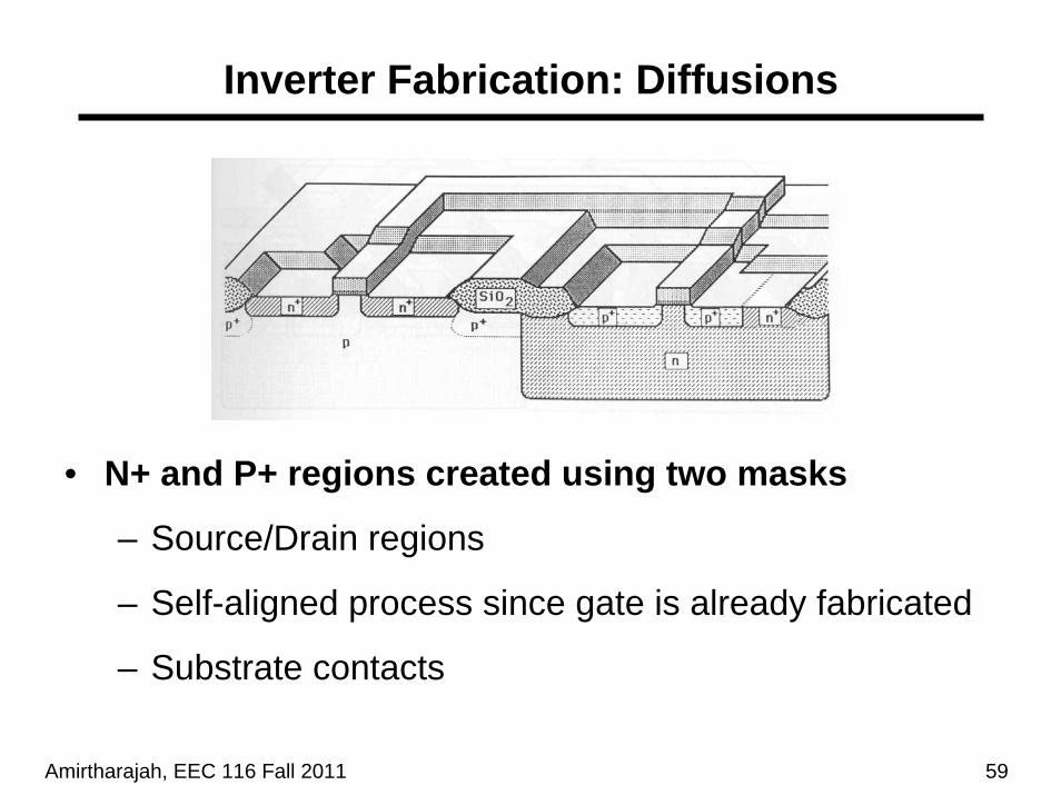
Inverter Fabrication: Diffusions
• N+ and P+ regions created using two masks
– Source/Drain regions
– Self-aligned process since gate is already fabricated
– Substrate contacts
Amirtharajah, EEC 116 Fall 2011 60
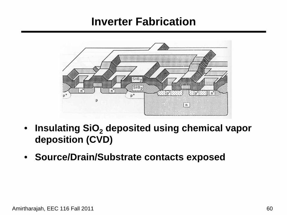
Inverter Fabrication
• Insulating SiO2 deposited using chemical vapor deposition (CVD)
• Source/Drain/Substrate contacts exposed
Amirtharajah, EEC 116 Fall 2011 61
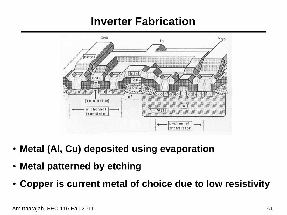
Inverter Fabrication
• Metal (Al, Cu) deposited using evaporation
• Metal patterned by etching
• Copper is current metal of choice due to low resistivity
Amirtharajah, EEC 116 Fall 2011 62
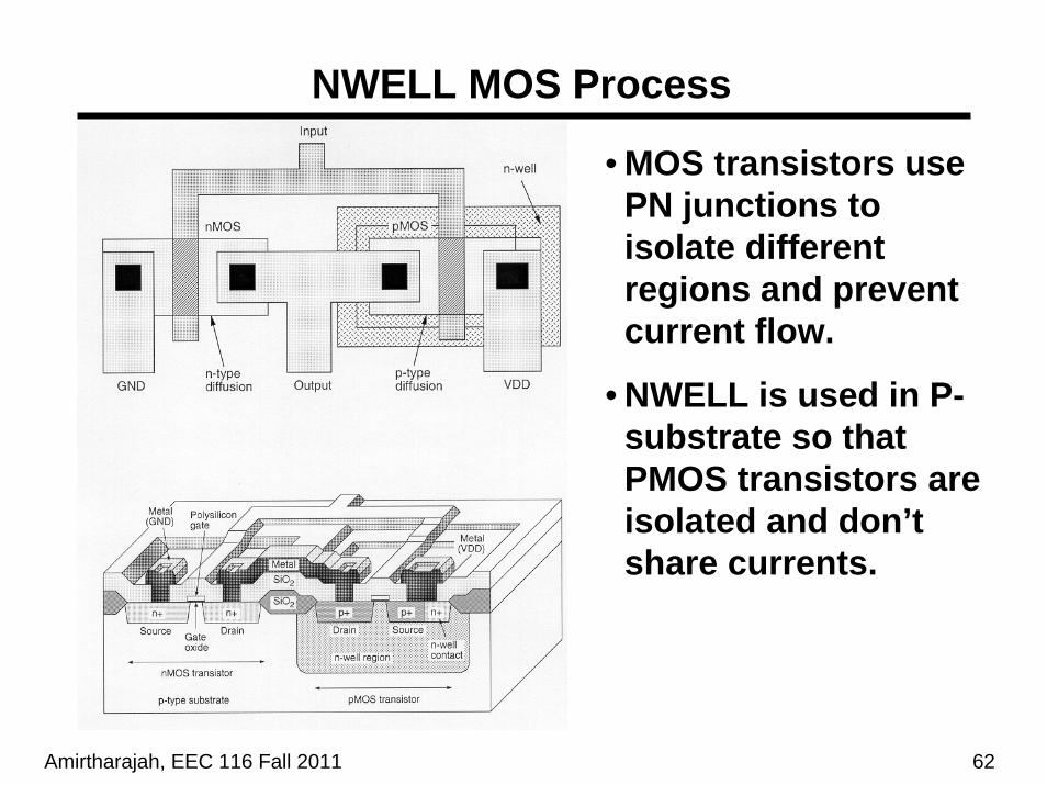
NWELL MOS Process
• MOS transistors use PN junctions to isolate different regions and prevent current flow.
• NWELL is used in P-substrate so that PMOS transistors are isolated and don’t share currents.
Amirtharajah, EEC 116 Fall 2011 63
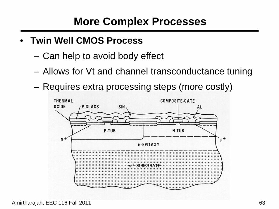
More Complex Processes• Twin Well CMOS Process
– Can help to avoid body effect– Allows for Vt and channel transconductance tuning– Requires extra processing steps (more costly)

Amirtharajah, EEC 116 Fall 2011 64
Silicon-On-Insulator (SOI) Process
• Both transistors built on insulating substrate
– Allows for tight compaction of design area
– Some of the parasitic capacitances seen in bulk CMOS disappear
– Wafer cost is high (IBM produces SOI, Intel doesn’t)
Amirtharajah, EEC 116 Fall 2011 65
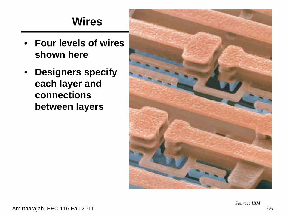
Wires
• Four levels of wires shown here
• Designers specify each layer and connections between layers
Source: IBM

Amirtharajah, EEC 116 Fall 2011 66
• Modern chips have up to 8 layers of wires
Source: IBM
Chip Wires
Amirtharajah, EEC 116 Fall 2011 67
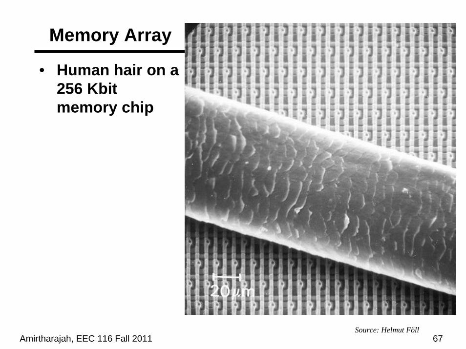
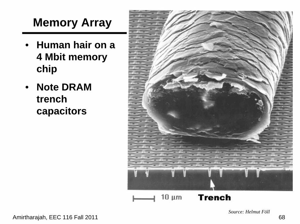
Memory Array
• Human hair on a 256 Kbit memory chip
Source: Helmut Föll
Amirtharajah, EEC 116 Fall 2011 68
Memory Array
• Human hair on a 4 Mbit memory chip
• Note DRAM trench capacitors
Source: Helmut Föll
Amirtharajah, EEC 116 Fall 2011 69
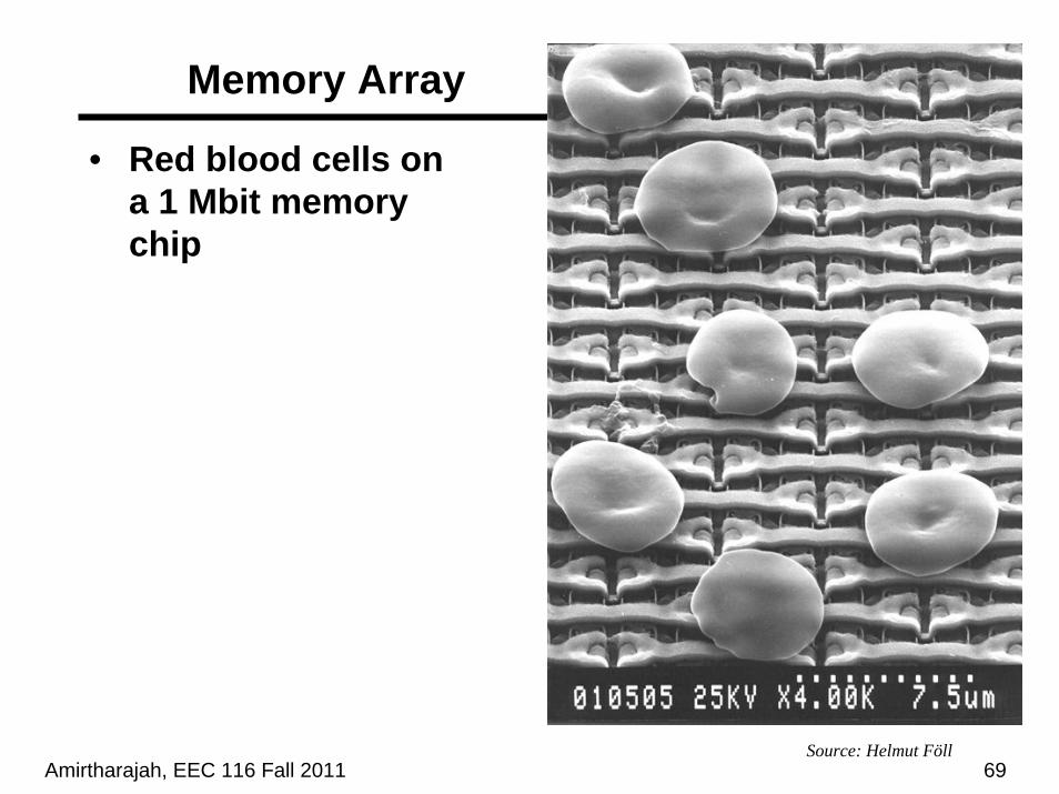
Memory Array
• Red blood cells on a 1 Mbit memory chip
Source: Helmut Föll
Amirtharajah, EEC 116 Fall 2011 70
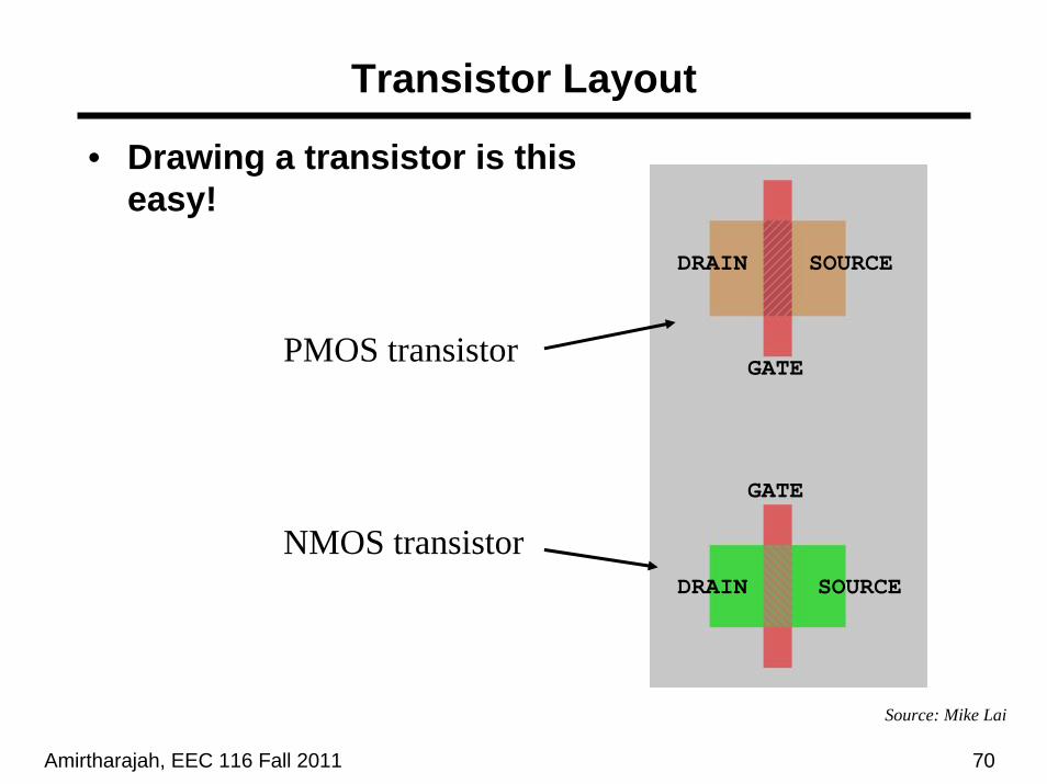
Transistor Layout
• Drawing a transistor is this easy!
Source: Mike Lai
PMOS transistor
NMOS transistor
GATE
GATE
DRAIN
DRAIN SOURCE
SOURCE
Amirtharajah, EEC 116 Fall 2011 71
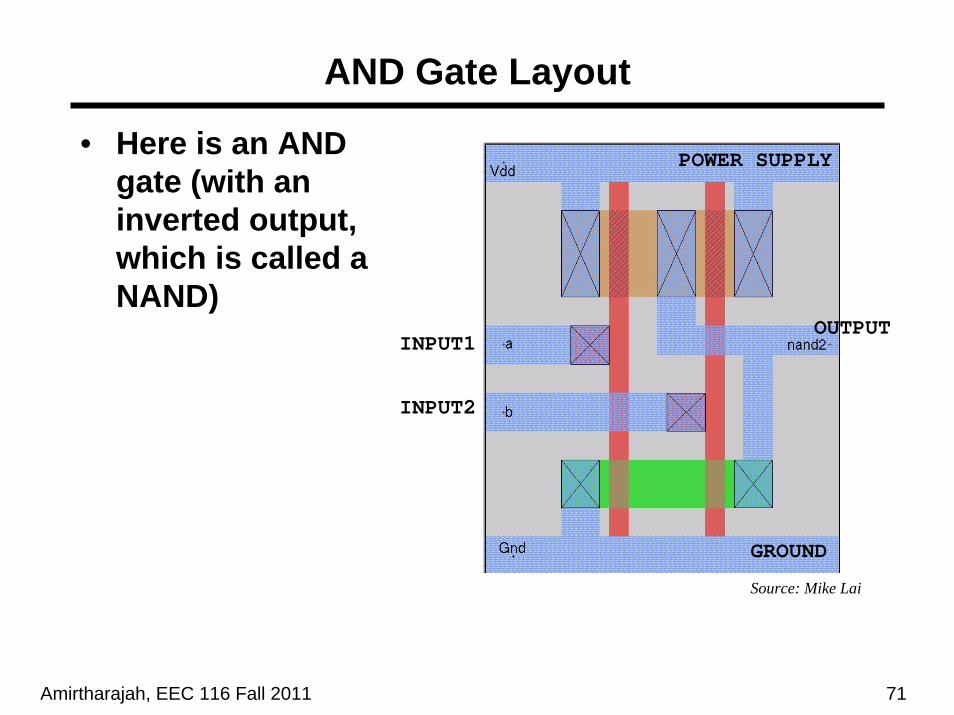
AND Gate Layout
• Here is an AND gate (with an inverted output, which is called a NAND)
Source: Mike Lai
OUTPUT
POWER SUPPLY
GROUND
INPUT1
INPUT2
Amirtharajah, EEC 116 Fall 2011 72
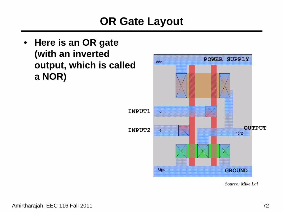
OR Gate Layout
• Here is an OR gate (with an inverted output, which is called a NOR)
Source: Mike Lai
OUTPUT
POWER SUPPLY
GROUND
INPUT1
INPUT2
Amirtharajah, EEC 116 Fall 2011 73
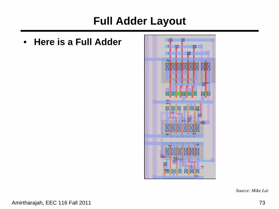
Full Adder Layout
• Here is a Full Adder
Source: Mike Lai

Amirtharajah, EEC 116 Fall 2011 74
16-bit Adder Layout
• Here is a complete 16-bit adder (it adds two numbers where each input can range from –32,000 to +32,000)
• This adder contains 16 full adders (essentially) plus additional circuits for fast addition
Source: Mike Lai
Amirtharajah, EEC 116 Fall 2011 75
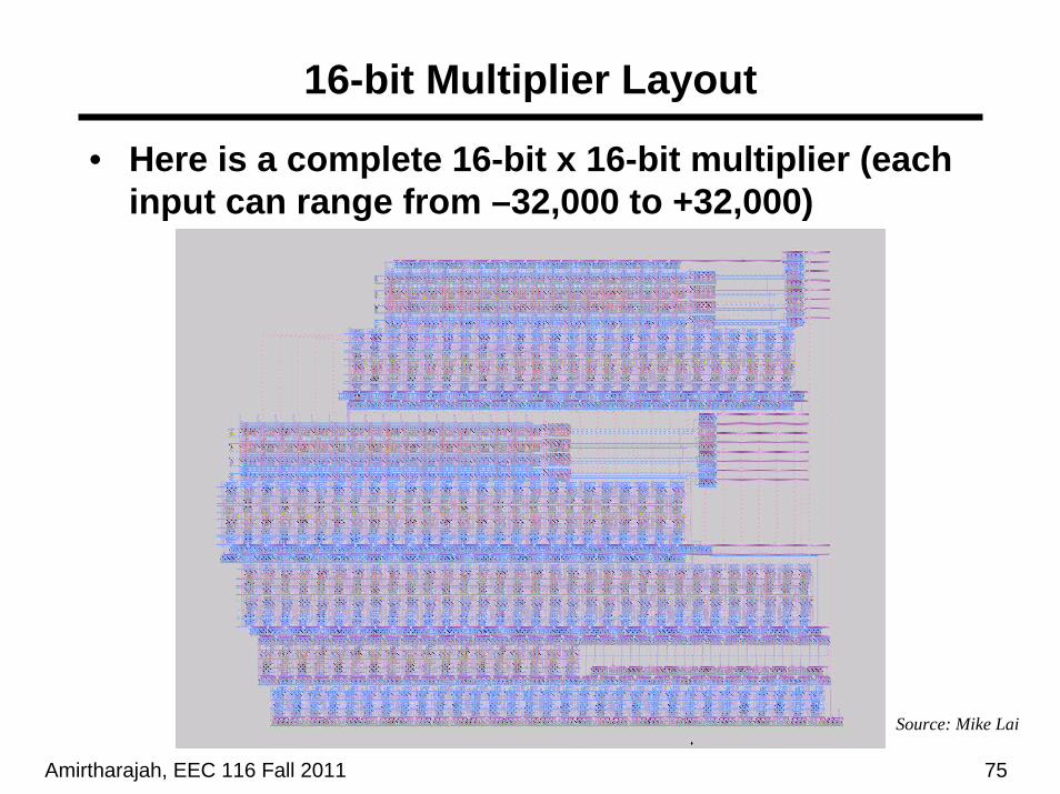
16-bit Multiplier Layout
• Here is a complete 16-bit x 16-bit multiplier (each input can range from –32,000 to +32,000)
Source: Mike Lai
Amirtharajah, EEC 116 Fall 2011 76
Next Topic: MOSFETs and Inverters
• Inverter Layout
• MOS Structure
• Inverter Characteristics
– Transfer functions, noise margins
• CMOS Inverters