eecs 142 lecture 9: intercept point, gain compression and blocking
TRANSCRIPT

EECS 142
Lecture 9: Intercept Point, Gain Compression andBlocking
Prof. Ali M. Niknejad
University of California, Berkeley
Copyright c© 2005 by Ali M. Niknejad
A. M. Niknejad University of California, Berkeley EECS 142 Lecture 9 p. 1/29 – p. 1/29

Gain Compression
Vi
Vo
dVo
dVi
Vi
Vo
dVo
dVi
The large signal input/output relation can display gaincompression or expansion. Physically, most amplifierexperience gain compression for large signals.
The small-signal gain is related to the slope at a givenpoint. For the graph on the left, the gain decreases forincreasing amplitude.
A. M. Niknejad University of California, Berkeley EECS 142 Lecture 9 p. 2/29 – p. 2/29

1 dB Compression Point
∣
∣
∣
∣
Vo
Vi
∣
∣
∣
∣
Vi
Po,−1 dB
Pi,−1 dB
Gain compression occurs because eventually theoutput signal (voltage, current, power) limits, due to thesupply voltage or bias current.
If we plot the gain (log scale) as a function of the inputpower, we identify the point where the gain has droppedby 1 dB. This is the 1 dB compression point. It’s a veryimportant number to keep in mind.
A. M. Niknejad University of California, Berkeley EECS 142 Lecture 9 p. 3/29 – p. 3/29

Apparent Gain
Recall that around a small deviation, the large signalcurve is described by a polynomial
so = a1si + a2s2i + a3s
3i + · · ·
For an input si = S1 cos(ω1t), the cubic term generates
S31 cos3(ω1t) = S3
1 cos(ω1t)1
2(1 + cos(2ω1t))
= S31
(1
2cos(ω1t) +
2
4cos(ω1t) cos(2ω1t)
)
Recall that 2 cos a cos b = cos(a + b) + cos(a − b)
= S31
(1
2cos(ω1t) +
1
4(cos(ω1t) + cos(3ω1t))
)
A. M. Niknejad University of California, Berkeley EECS 142 Lecture 9 p. 4/29 – p. 4/29
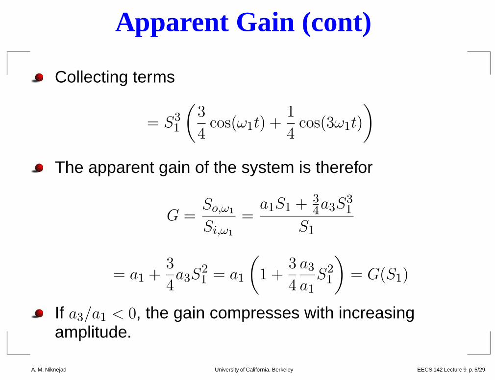
Apparent Gain (cont)
Collecting terms
= S31
(3
4cos(ω1t) +
1
4cos(3ω1t)
)
The apparent gain of the system is therefor
G =So,ω1
Si,ω1
=a1S1 + 3
4a3S
31
S1
= a1 +3
4a3S
21 = a1
(
1 +3
4
a3
a1
S21
)
= G(S1)
If a3/a1 < 0, the gain compresses with increasingamplitude.
A. M. Niknejad University of California, Berkeley EECS 142 Lecture 9 p. 5/29 – p. 5/29

1-dB Compression Point
Let’s find the input level where the gain has dropped by1 dB
20 log
(
1 +3
4
a3
a1
S21
)
= −1 dB
3
4
a3
a1
S21 = −0.11
S1 =
√
4
3
∣∣∣∣
a1
a3
∣∣∣∣×√
0.11 = IIP3 − 9.6 dB
The term in the square root is called the third-orderintercept point (see next few slides).
A. M. Niknejad University of California, Berkeley EECS 142 Lecture 9 p. 6/29 – p. 6/29

Intercept Point IP2
-50 -40 -30 -20 -10
-40
-30
-20
-10
0
dBc
IP2
Pin
(dBm)
Pout
(dBm)
IIP2
OIP2
dBc
10
20
10
Fund
2n
d
The extrapolated point where IM2 = 0 dBc is known asthe second order intercept point IP2.
A. M. Niknejad University of California, Berkeley EECS 142 Lecture 9 p. 7/29 – p. 7/29

Properties of Intercept Point IP2
Since the second order IM distortion products increaselike s2
i , we expect that at some power level the distortionproducts will overtake the fundamental signal.
The extrapolated point where the curves of thefundamental signal and second order distortion productsignal meet is the Intercept Point (IP2).
At this point, then, by definition IM2 = 0 dBc.
The input power level is known as IIP2, and the outputpower when this occurs is the OIP2 point.
Once the IP2 point is known, the IM2 at any otherpower level can be calculated. Note that for a dBback-off from the IP2 point, the IM2 improves dB for dB
A. M. Niknejad University of California, Berkeley EECS 142 Lecture 9 p. 8/29 – p. 8/29

Intercept Point IP3
-50 -40 -30 -20 -10
-30
-20
-10
0
10
dBc
IP3
Pin
(dBm)
Pout
(dBm)
IIP3
OIP3
dBc
20Fund
Third
The extrapolated point where IM3 = 0 dBc is known asthe third-order intercept point IP3.
A. M. Niknejad University of California, Berkeley EECS 142 Lecture 9 p. 9/29 – p. 9/29

Properties of Intercept Point IP3
Since the third order IM distortion products increase likes3i , we expect that at some power level the distortion
products will overtake the fundamental signal.
The extrapolated point where the curves of thefundamental signal and third order distortion productsignal meet is the Intercept Point (IP3).
At this point, then, by definition IM3 = 0 dBc.
The input power level is known as IIP3, and the outputpower when this occurs is the OIP3 point.
Once the IP3 point is known, the IM3 at any otherpower level can be calculated. Note that for a 10 dBback-off from the IP3 point, the IM3 improves 20 dB.
A. M. Niknejad University of California, Berkeley EECS 142 Lecture 9 p. 10/29 – p. 10/29

Intercept Point Example
From the previous graph we see that our amplifier hasan IIP3 = −10 dBm.
What’s the IM3 for an input power of Pin = −20 dBm?
Since the IM3 improves by 20 dB for every 10 dBback-off, it’s clear that IM3 = 20 dBc
What’s the IM3 for an input power of Pin = −110 dBm?
Since the IM3 improves by 20 dB for every 10 dBback-off, it’s clear that IM3 = 200 dBc
A. M. Niknejad University of California, Berkeley EECS 142 Lecture 9 p. 11/29 – p. 11/29

Calculated IIP2/IIP3
We can also calculate the IIP points directly from ourpower series expansion. By definition, the IIP2 pointoccurs when
IM2 = 1 =a2
a1
Si
Solving for the input signal level
IIP2 = Si =a1
a2
In a like manner, we can calculate IIP3
IM3 = 1 =3
4
a3
a1
S2i IIP3 = Si =
√
4
3
∣∣∣∣
a1
a3
∣∣∣∣
A. M. Niknejad University of California, Berkeley EECS 142 Lecture 9 p. 12/29 – p. 12/29

Blocker or Jammer
Signal
Interference
channel
LNA
Consider the input spectrum of a weak desired signaland a “blocker”
Si = S1 cos ω1t︸ ︷︷ ︸
Blocker
+ s2 cos ω2t︸ ︷︷ ︸
Desired
We shall show that in the presence of a stronginterferer, the gain of the system for the desired signalis reduced. This is true even if the interference signal isat a substantially difference frequency. We call thisinterference signal a “jammer”.
A. M. Niknejad University of California, Berkeley EECS 142 Lecture 9 p. 13/29 – p. 13/29
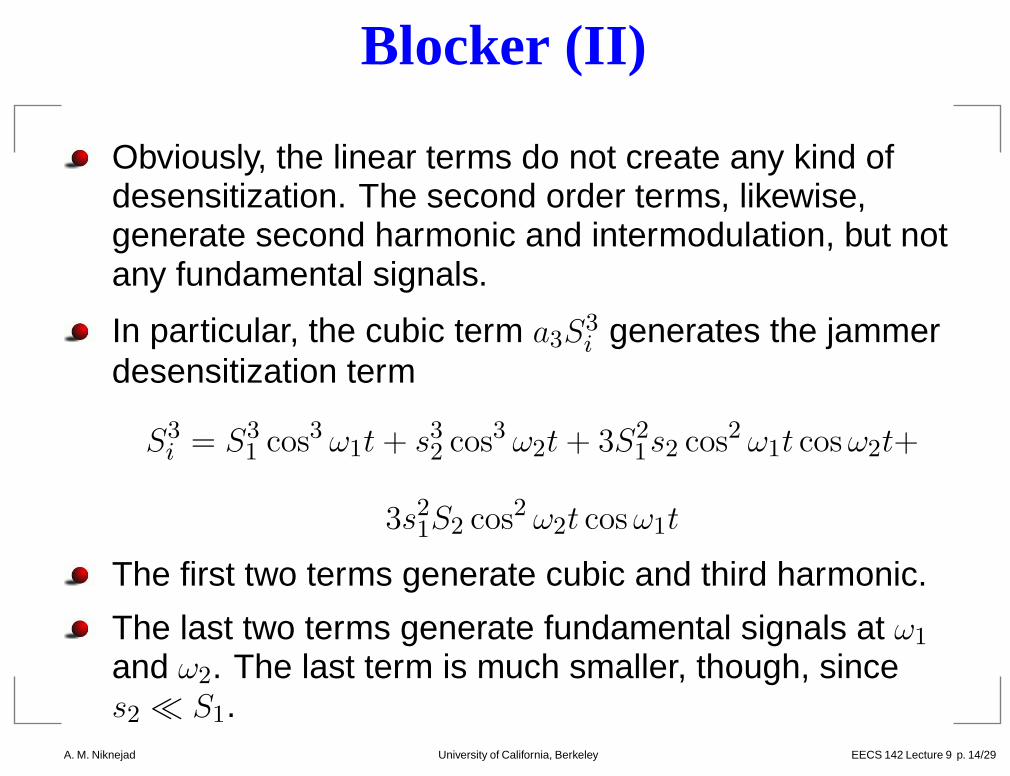
Blocker (II)
Obviously, the linear terms do not create any kind ofdesensitization. The second order terms, likewise,generate second harmonic and intermodulation, but notany fundamental signals.
In particular, the cubic term a3S3i generates the jammer
desensitization term
S3i = S3
1 cos3 ω1t + s32 cos3 ω2t + 3S2
1s2 cos2 ω1t cos ω2t+
3s21S2 cos2 ω2t cos ω1t
The first two terms generate cubic and third harmonic.
The last two terms generate fundamental signals at ω1
and ω2. The last term is much smaller, though, sinces2 ≪ S1.
A. M. Niknejad University of California, Berkeley EECS 142 Lecture 9 p. 14/29 – p. 14/29

Blocker (III)
The blocker term is therefore given by
a33S21s2
1
2cos ω2t
This term adds or subtracts from the desired signal.Since a3 < 0 for most systems (compressivenon-linearity), the effect of the blocker is to reduce thegain
App Gain =a1s2 + a3
3
2S2
1s2
s2
= a1 + a3
3
2S2
1 = a1
(
1 +3
2
a3
a1
S21
)
A. M. Niknejad University of California, Berkeley EECS 142 Lecture 9 p. 15/29 – p. 15/29

Out of Band 3 dB Desensitization
Let’s find the blocker power necessary to desensitizethe amplifier by 3 dB. Solving the above equation
20 log
(
1 +3
2
a3
a1
S21
)
= −3 dB
We find that the blocker power is given by
POB = P−1 dB + 1.2 dB
It’s now clear that we should avoid operating ouramplifier with any signals in the vicinity of P
−1 dB, sincegain reduction occurs if the signals are larger. At thissignal level there is also considerable intermodulationdistortion.
A. M. Niknejad University of California, Berkeley EECS 142 Lecture 9 p. 16/29 – p. 16/29

Series Inversion
Often it’s easier to find a power series relation for theinput in terms of the output. In other words
Si = a1So + a2S2o + a3S
3o + · · ·
But we desire the inverse relation
So = b1Si + b2S2i + b3S
3i + · · ·
To find the inverse relation, we can substitute the aboveequation into the original equation and equatecoefficient of like powers.
Si = a1(b1Si + b2S2i + b3S
3i + · · · ) + a2( )2 + a3( )3 + · · ·
A. M. Niknejad University of California, Berkeley EECS 142 Lecture 9 p. 17/29 – p. 17/29

Inversion (cont)Equating linear terms, we find, as expected, thata1b1 = 1, or b1 = 1/a1.
Equating the square terms, we have
0 = a1b2 + a2b21
b2 = −a2b
21
a1
= −a2
a31
Finally, equating the cubic terms we have
0 = a1b3 + a22b1b2 + a3b31
b3 =2a2
2
a51
−a3
a41
It’s interesting to note that if one power series does nothave cubic, a3 ≡ 0, the inverse series has cubic due tothe first term above.
A. M. Niknejad University of California, Berkeley EECS 142 Lecture 9 p. 18/29 – p. 18/29
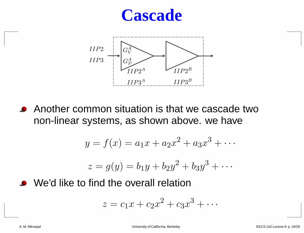
Cascade
IIP2A
IIP3A
IIP2B
IIP3B
IIP2
IIP3
GAV
GAP
Another common situation is that we cascade twonon-linear systems, as shown above. we have
y = f(x) = a1x + a2x2 + a3x
3 + · · ·
z = g(y) = b1y + b2y2 + b3y
3 + · · ·
We’d like to find the overall relation
z = c1x + c2x2 + c3x
3 + · · ·
A. M. Niknejad University of California, Berkeley EECS 142 Lecture 9 p. 19/29 – p. 19/29

Cascade Power SeriesTo find c1, c2, · · · , we simply substitute one power seriesinto the other and collect like powers.
The linear terms, as expected, are given by
c1 = b1a1 = a1b1
The square terms are given by
c2 = b1a2 + b2a21
The first term is simply the second order distortionproduced by the first amplifier and amplified by thesecond amplifier linear term. The second term is thegeneration of second order by the second amplifier.
A. M. Niknejad University of California, Berkeley EECS 142 Lecture 9 p. 20/29 – p. 20/29
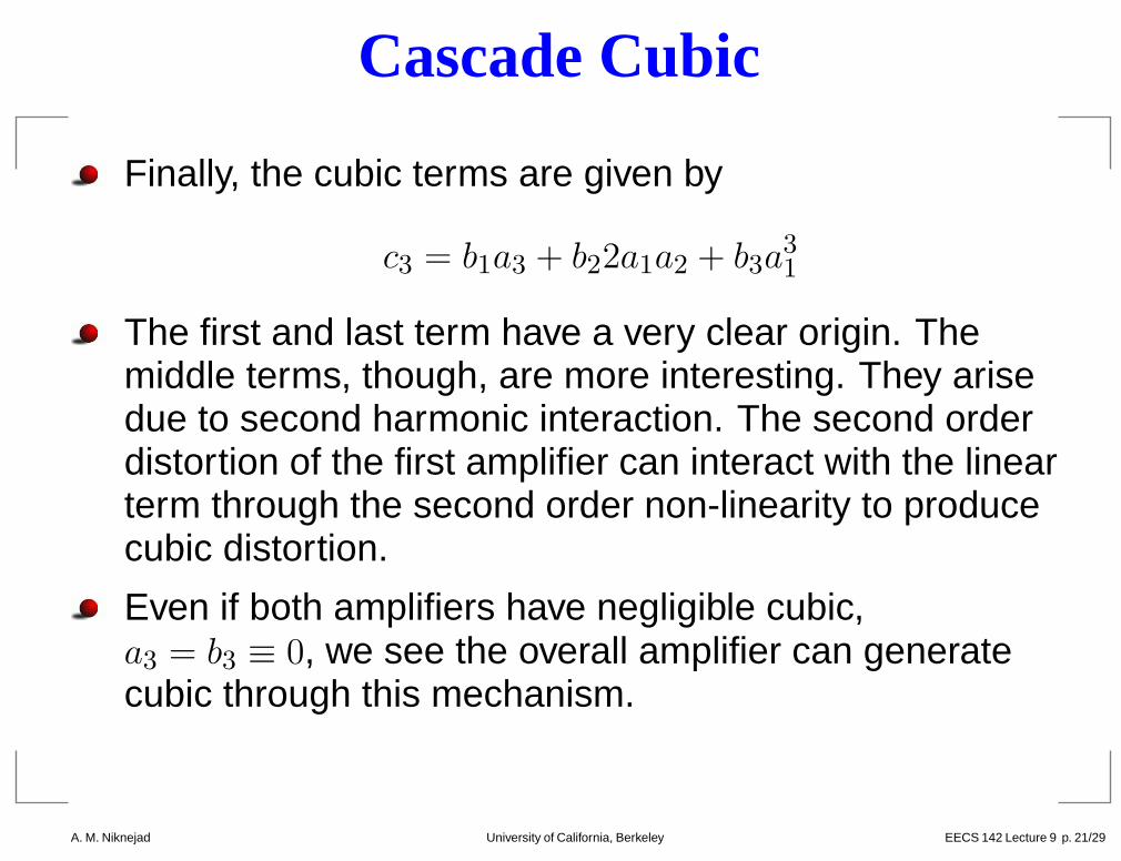
Cascade Cubic
Finally, the cubic terms are given by
c3 = b1a3 + b22a1a2 + b3a31
The first and last term have a very clear origin. Themiddle terms, though, are more interesting. They arisedue to second harmonic interaction. The second orderdistortion of the first amplifier can interact with the linearterm through the second order non-linearity to producecubic distortion.
Even if both amplifiers have negligible cubic,a3 = b3 ≡ 0, we see the overall amplifier can generatecubic through this mechanism.
A. M. Niknejad University of California, Berkeley EECS 142 Lecture 9 p. 21/29 – p. 21/29

Cascade Example
In the above amplifier, we can decompose thenon-linearity as a cascade of two non-linearities, the Gm
non-linearity
id = Gm1vin + Gm2v2in + Gm3v
3in + · · ·
And the output impedance non-linearity
vo = R1id + R2i2
d + R3i3
d + · · ·
The output impedance can be a non-linear resistor load(such as a current mirror) or simply the load of thedevice itself, which has a non-linear component.
A. M. Niknejad University of California, Berkeley EECS 142 Lecture 9 p. 22/29 – p. 22/29

IIP2 Cascade
Commonly we’d like to know the performance of acascade in terms of the overall IIP2. To do this, notethat IIP2 = c1/c2
c2
c1
=b1a2 + b2a
21
b1a1
=a2
a1
+b2
b1
a1
This leads to
1
IIP2=
1
IIP2A+
a1
IIP2B
This is a very intuitive result, since it simply says thatwe can input refer the IIP2 of the second amplifier tothe input by the voltage gain of the first amplifier.
A. M. Niknejad University of California, Berkeley EECS 142 Lecture 9 p. 23/29 – p. 23/29

IIP2 Cascade ExampleExample 1: Suppose the input amplifiers of a cascadehas IIP2A = +0 dBm and a voltage gain of 20 dB. Thesecond amplifier has IIP2B = +10 dBm.
The input referred IIP2Bi = 10 dBm − 20 dB = −10 dBm
This is a much smaller signal than the IIP2A, so clearlythe second amplifier dominates the distortion. Theoverall distortion is given by IIP2 ≈ −12 dB.
Example 2: Now suppose IIP2B = +20 dBm. SinceIIP2B
i = 20 dBm − 20 dB = 0 dBm, we cannot assumethat either amplifier dominates.
Using the formula, we see the actual IIP2 of thecascade is a factor of 2 down, IIP2 = −3 dBm.
A. M. Niknejad University of California, Berkeley EECS 142 Lecture 9 p. 24/29 – p. 24/29

IIP3 Cascade
Using the same approach, let’s start with
c3
c1
=b1a3 + b2a1a22 + b3a
31
baa1
=
(a3
a1
+b3
b1
a21 +
b2
b1
2a2
)
The last term, the second harmonic interaction term,will be neglected for simplicity. Then we have
1
IIP32=
1
IIP32
A
+a2
1
IIP32
B
Which shows that the IIP3 of the second amplifier isinput referred by the voltage gain squared, or the powergain.
A. M. Niknejad University of California, Berkeley EECS 142 Lecture 9 p. 25/29 – p. 25/29

LNA/Mixer Example
A common situation is an LNA and mixer cascade. Themixer can be characterized as a non-linear block with agiven IIP2 and IIP3.
In the above example, the LNA has anIIP3A = −10 dBm and a power gain of 20 dB. The mixerhas an IIP3B = −20 dBm.
If we input refer the mixer, we haveIIP3B
i = −20 dBm − 20 dB = −40 dBm.
The mixer will dominate the overall IIP3 of the system.
A. M. Niknejad University of California, Berkeley EECS 142 Lecture 9 p. 26/29 – p. 26/29

Example: Disto in Long-Ch. MOS Amp
vi
VQ
ID = IQ + io
ID = 1
2µCox
W
L(VGS − VT )2
io+IQ = 1
2µCox
W
L(VQ+vi−VT )2
Ignoring the output impedance we have
= 1
2µCox
W
L
(VQ − VT )2 + v2
i + 2vi(VQ − VT )
= IQ︸︷︷︸
dc
+ µCoxW
Lvi(VQ − VT )
︸ ︷︷ ︸
linear
+ 1
2µCox
W
Lv2i
︸ ︷︷ ︸
quadraticA. M. Niknejad University of California, Berkeley EECS 142 Lecture 9 p. 27/29 – p. 27/29

Ideal Square Law Device
An ideal square law device only generates 2nd orderdistortion
io = gmvi + 1
2µCox
W
Lv2i
a1 = gm
a2 = 1
2µCox
W
L= 1
2
gm
VQ − VT
a3 ≡ 0
The harmonic distortion is given by
HD2 =1
2
a2
a1
vi =1
4
gm
VQ − VT
1
gmvi =
1
4
vi
VQ − VT
HD3 = 0A. M. Niknejad University of California, Berkeley EECS 142 Lecture 9 p. 28/29 – p. 28/29

Real MOSFET Device
0
200
400
600
Effective Field
Mo
bili
ty
Triode CLM DIBL SCBE
Rou
tkΩ
Vds (V)
2
4
6
8
10
12
14
0 1 2 3 4
The real MOSFET device generates higher orderdistortion
The output impedance is non-linear. The mobility µ isnot a constant but a function of the vertical andhorizontal electric field
We may also bias the device at moderate or weakinversion, where the device behavior is moreexponential
There is also internal feedbackA. M. Niknejad University of California, Berkeley EECS 142 Lecture 9 p. 29/29 – p. 29/29