eem336 microprocessors i - ceng anadoluceng.anadolu.edu.tr/abilge/bim303/icerik/bim303 - 07 -...
TRANSCRIPT

EEM336 Microprocessors I
Memory Interface

EEM336 Microprocessors I 2Memory Interface
Introduction• Simple or complex, every microprocessor-
based system has a memory system. • Almost all systems contain two main types of
memory: read-only memory (ROM) and random access memory (RAM) or read/write memory.
• This chapter explains how to interface both memory types to the Intel family of microprocessors.

EEM336 Microprocessors I 3Memory Interface
Chapter Objectives
• Decode the memory address and use the outputs of the decoder to select various memory components.
• Use programmable logic devices (PLDs) to decode memory addresses.
• Explain how error correction code (ECC) is used with memory.
Upon completion of this chapter, you will be able to:

EEM336 Microprocessors I 4Memory Interface
MEMORY DEVICES • Before attempting to interface memory to the
microprocessor, it is essential to understand the operation of memory components.
• In this section, we explain functions of thefour common types of memory: – Read-Only Memory (ROM) – Flash Memory (EEPROM) – Static Random Access Memory (SRAM)– Dynamic Random Access Memory (DRAM)

EEM336 Microprocessors I 5Memory Interface
Figure. A pseudomemory component illustrating the address, data, and control connections.
Memory Pin Connections – address inputs– data outputs or
input/outputs– some type of selection
input– at least one control
input to select a read or write operation

EEM336 Microprocessors I 6Memory Interface
Address Connections• Memory devices have address inputs to
select a memory location within the device. • Almost always labeled from A0, the least
significant address input, to An– where subscript n can be any value– always labeled as one less than total number
of address pins• A memory device with 10 address pins has
its address pins labeled from A0 to A9.

EEM336 Microprocessors I 7Memory Interface
• The number of address pins on a memory device is determined by the number of memory locations found within it.
• Today, memory devices have memory locations starting from 1K to multiple G.
• A 1K memory device has 10 address pins.– therefore, 10 address inputs are required to
select any of its 1024 memory locations
EEM336 Microprocessors I 8Memory Interface
• It takes a 10-bit binary number to select any single location on a 1024-location device. – 1024 different combinations– if a device has 11 address connections, it
has 2048 (2K) internal memory locations• The number of memory locations can be
extrapolated from the number of pins.

EEM336 Microprocessors I 9Memory Interface
Data Connections• All memory devices have a set of data
outputs or input/outputs.– today, many devices have bidirectional
common I/O pins– data connections are points at which data are
entered for storage or extracted for reading• Data pins on memory devices are labeled D0
through D7 for an 8-bit-wide memory device.
EEM336 Microprocessors I 10Memory Interface
• An 8-bit-wide memory device is often called a byte-wide memory. – most devices are currently 8 bits wide, – some are 16 bits, 4 bits, or just 1 bit wide
• Catalog listings of memory devices often refer to memory locations times bits per location.– a memory device with 1K memory locations
and 8 bits in each location is often listed asa 1K 8 by the manufacturer
• Memory devices are often classified according to total bit capacity.

EEM336 Microprocessors I 11Memory Interface
Selection Connections• Each memory device has an input that selects
or enables the memory device. – sometimes more than one
• This type of input is most often called a chip select (G2A) chip enable (CE) or simply select (S) input.
• RAM memory generally has at least one or input, and ROM has at least one
• If more than one CE connection is present,all must be activated to read or write data.

EEM336 Microprocessors I 12Memory Interface
Control Connections• All memory devices have some form of control
input or inputs. – ROM usually has one control input, while RAM
often has one or two control inputs• Control input often found on ROM is the
output enable or gate connection, which allows data flow from output data pins.
• The OE connection enables and disables a set of three-state buffers located in the device and must be active to read data.

EEM336 Microprocessors I 13Memory Interface
• RAM has either one or two control inputs. – if one control input, it is often called R/W
• If the RAM has two control inputs, they are usually labeled WE (or W ), and OE (or G ).– write enable must be active to perform memory
write, and OE active to perform a memory read – when the two controls are present, they must
never both be active at the same time • If both inputs are inactive, data are neither
written nor read.– the connections are at their high-impedance state

EEM336 Microprocessors I 14Memory Interface
Sample Memory Read/Write Timing Cycles

EEM336 Microprocessors I 15Memory Interface
Datasheets
• You can get detailed information on ICs including memory units by just looking at their datasheets.
• Every manufacturer releases datasheets of their products which includes operational information.

EEM336 Microprocessors I 16Memory Interface
ROM Memory • Read-only memory (ROM) permanently
stores programs/data resident to the system. – and must not change when power disconnected
• Often called nonvolatile memory, because its contents do not change even if power is disconnected.
• A device we call a ROM is purchased in mass quantities from a manufacturer.– programmed during fabrication at the factory

EEM336 Microprocessors I 17Memory Interface
• The EPROM (erasable programmable read-only memory) is commonly used when software must be changed often.– or when low demand makes ROM uneconomical– for ROM to be practical at least 10,000 devices
must be sold to recoup factory charges • An EPROM is programmed in the field on a
device called an EPROM programmer.• Also erasable if exposed to high-intensity
ultraviolet light.– depending on the type of EPROM
EEM336 Microprocessors I 18Memory Interface
• PROM memory devices are also available, although they are not as common today.
• The PROM (programmable read-only memory) is also programmed in the field by burning open tiny NI-chrome or silicon oxide fuses.
• Once it is programmed, it cannot be erased.

EEM336 Microprocessors I 19Memory Interface
• A newer type of read-mostly memory(RMM) is called the flash memory. – also often called an EEPROM (electrically
erasable programmable ROM)– EAROM (electrically alterable ROM)– or a NOVRAM (nonvolatile RAM)
• Electrically erasable in the system, but they require more time to erase than normal RAM.
• The flash memory device is used to store setup information for systems such as the video card in the computer.
EEM336 Microprocessors I 20Memory Interface
• Flash has all but replaced the EPROM in most computer systems for the BIOS. – some systems contain a password stored
in the flash memory device• Flash memory has its biggest impact in
memory cards for digital cameras and memory in MP3 audio players.

EEM336 Microprocessors I 21Memory Interface
• The basic speed of a common 2716 EPROM is 450 ns.
• This type of component requires wait statesto operate properly with a processor because of its rather long access time. – if wait states are not desired, higher-speed
EPROMs are available at additional cost – EPROM memory is available with access times
of as little as 100 ns• Obviously, wait states are required in modern
microprocessors for any EPROM device.

EEM336 Microprocessors I 22Memory Interface
Static RAM (SRAM) Devices • Static RAM memory devices retain data
as long as DC power is applied. • Because no special action is required to retain
data, these devices are called static memory. – also called volatile memory because they will
not retain data without power• The main difference between ROM and RAM
is that RAM is written under normal operation, whereas ROM is programmed outside the computer and normally is only read.

EEM336 Microprocessors I 23Memory Interface
• Access time on a typical 4016 SRAM is 250 ns, fast enough to connect directly to an 8088/8086 at 5 MHz, without wait states.
• Access time must always be checked to determine compatibility of memory components
• Access times can be as low as 1.0 ns for SRAM used in computer cache memory
EEM336 Microprocessors I 24Memory Interface
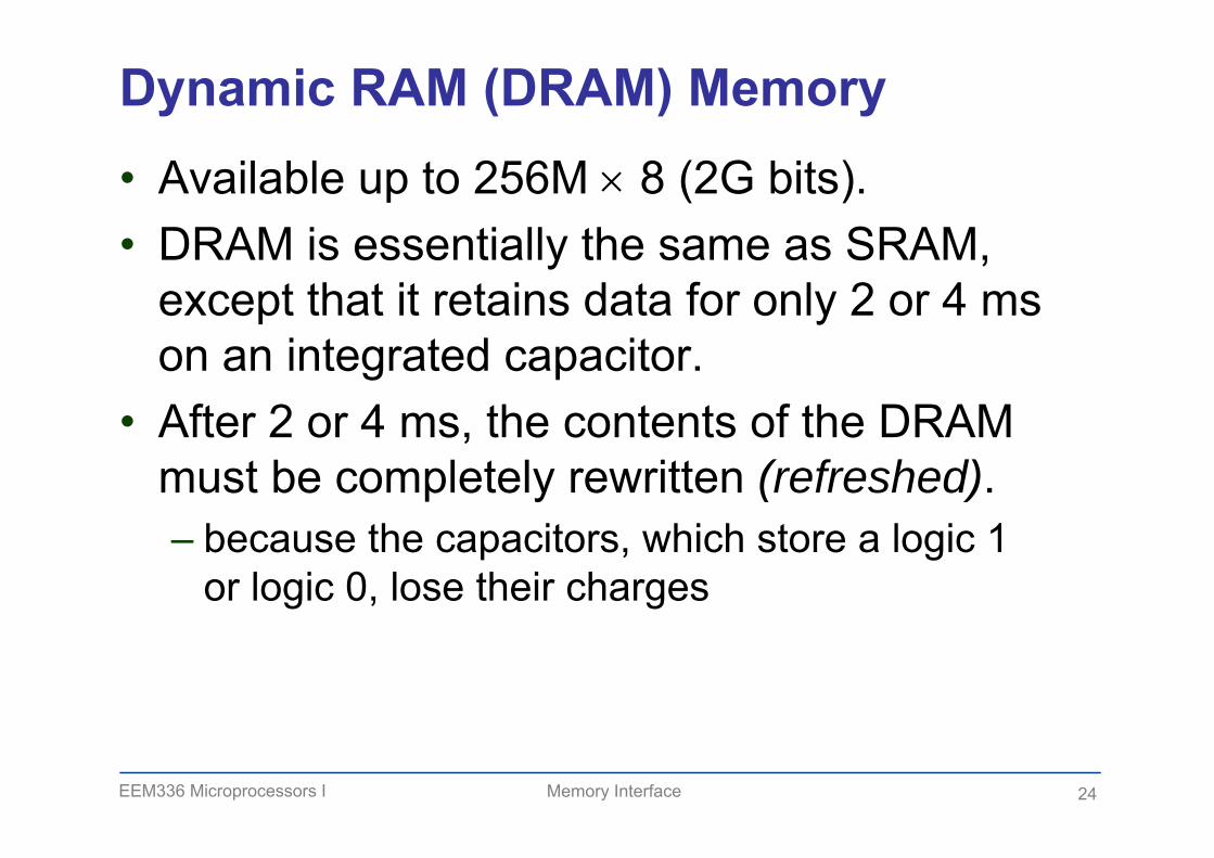
Dynamic RAM (DRAM) Memory • Available up to 256M 8 (2G bits). • DRAM is essentially the same as SRAM,
except that it retains data for only 2 or 4 mson an integrated capacitor.
• After 2 or 4 ms, the contents of the DRAM must be completely rewritten (refreshed).– because the capacitors, which store a logic 1
or logic 0, lose their charges
EEM336 Microprocessors I 25Memory Interface
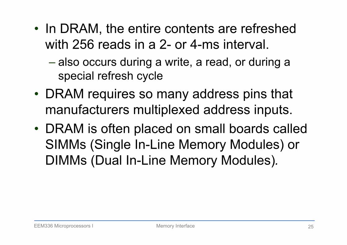
• In DRAM, the entire contents are refreshed with 256 reads in a 2- or 4-ms interval. – also occurs during a write, a read, or during a
special refresh cycle• DRAM requires so many address pins that
manufacturers multiplexed address inputs. • DRAM is often placed on small boards called
SIMMs (Single In-Line Memory Modules) or DIMMs (Dual In-Line Memory Modules).

EEM336 Microprocessors I 26Memory Interface
• Another type is the RIMM memory module from RAMBUS Corporation,– this memory type has faded from the market
• The latest DRAM is the DDR (double-data rate) memory device and DDR2. – DDR transfers data at each edge of the clock,
making it operate at twice the speed of SDRAM.
EEM336 Microprocessors I 27Memory Interface
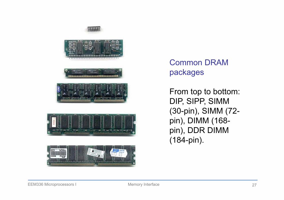
Common DRAM packages
From top to bottom: DIP, SIPP, SIMM (30-pin), SIMM (72-pin), DIMM (168-pin), DDR DIMM (184-pin).

EEM336 Microprocessors I 28Memory Interface
SRAM vs DRAM
• SRAM is static while DRAM is dynamic• SRAM is faster compared to DRAM• SRAM consumes less power than DRAM• SRAM uses more transistors per bit of memory
compared to DRAM• SRAM is more expensive than DRAM• Cheaper DRAM is used in main memory while
SRAM is commonly used in cache memory

EEM336 Microprocessors I 29Memory Interface
ADDRESS DECODING • In order to attach a memory device to the
microprocessor, it is necessary to decodethe address sent from the microprocessor.
• Decoding makes the memory function at a unique section or partition of the memory map.
• Without an address decoder, only onememory device can be connected to a microprocessor, which would make itvirtually useless.

EEM336 Microprocessors I 30Memory Interface
Why Decode Memory? • The 8088 has 20 address connections and
the 2716 EPROM has 11 connections.• The 8088 sends out a 20-bit memory
address whenever it reads or writes data. – because the 2716 has only 11 address pins,
there is a mismatch that must be corrected• The decoder corrects the mismatch by
decoding address pins that do not connectto the memory component.

EEM336 Microprocessors I 31Memory Interface
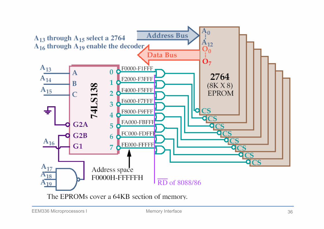
Simple NAND Gate Decoder • When the 2K 8 EPROM is used, address
connections A10–A0 of 8088 are connectedto address inputs A10–A0 of the EPROM. – the remaining nine address pins (A19–A11)
are connected to a NAND gate decoder• The decoder selects the EPROM from one of
the 2K-byte sections of the 1M-byte memory system in the 8088 microprocessor.
• In this circuit a NAND gate decodes the memory address, as seen in the figure.

EEM336 Microprocessors I 32Memory Interface
Figure. A simple NAND gate decoder that selects a 2716 EPROM for memory location FF800H–FFFFFH.

EEM336 Microprocessors I 33Memory Interface
• If the 20-bit binary address, decoded by the NAND gate, is written so that the leftmost nine bits are 1s and the rightmost 11 bits are don’t cares (X), the actual address range of the EPROM can be determined. – a don’t care is a logic 1 or a logic 0, whichever
is appropriate

EEM336 Microprocessors I 34Memory Interface

EEM336 Microprocessors I 35Memory Interface
The 3-to-8 Line Decoder (74LS138)
EEM336 Microprocessors I 36Memory Interface

EEM336 Microprocessors I 37Memory Interface
PLD Programmable Decoders • Three SPLD (simple PLD) devices function in
the same manner but have different names: – PLA (programmable logic array)– PAL (programmable array logic)– GAL (gated array logic)
• In existence since the mid-70s, they have appeared in memory system and digital designs since the early 1990s.

EEM336 Microprocessors I 38Memory Interface
• PAL and PLA are fuse-programmed, and some PLD devices are erasable devices.– all are arrays of programmable logic elements
• Other PLDs available:– CPLDs (complex programmable logic devices)– FPGAs (field programmable gate arrays) – FPICs (field programmable interconnect)
• These PLDs are more complex than the SPLDs used more commonly in designinga complete system.

EEM336 Microprocessors I 39Memory Interface
• If the concentration is on decoding addresses, the SPLD is used.
• If the concentration is on a complete system, then the CPLD, FPLG, or FPIC is used to implement the design.
• These devices are also referred to as an ASIC (application-specific integrated circuit).

EEM336 Microprocessors I 40Memory Interface
Error Detection and Correction• Parity, BCC (Block-Check Character) and CRC
(Cyclic Redundancy Check) are only mechanisms for error detection.
• The system is halted if an error is found in memory.• Error correction is starting to show up in new
systems.• SDRAM has ECC (Error Correction Code).• Correction will allow the system can continue
operating.• If two errors occur, they can be detected but not
corrected.• Error correction will of course cost more in terms of
extra bits.

EEM336 Microprocessors I 41Memory Interface
• Error correction is based on Hamming codes• Error detection and correction• Presumes one bit error most likely• Detects error and position
therefore allows for correction
Error Correction
EEM336 Microprocessors I 42Memory Interface
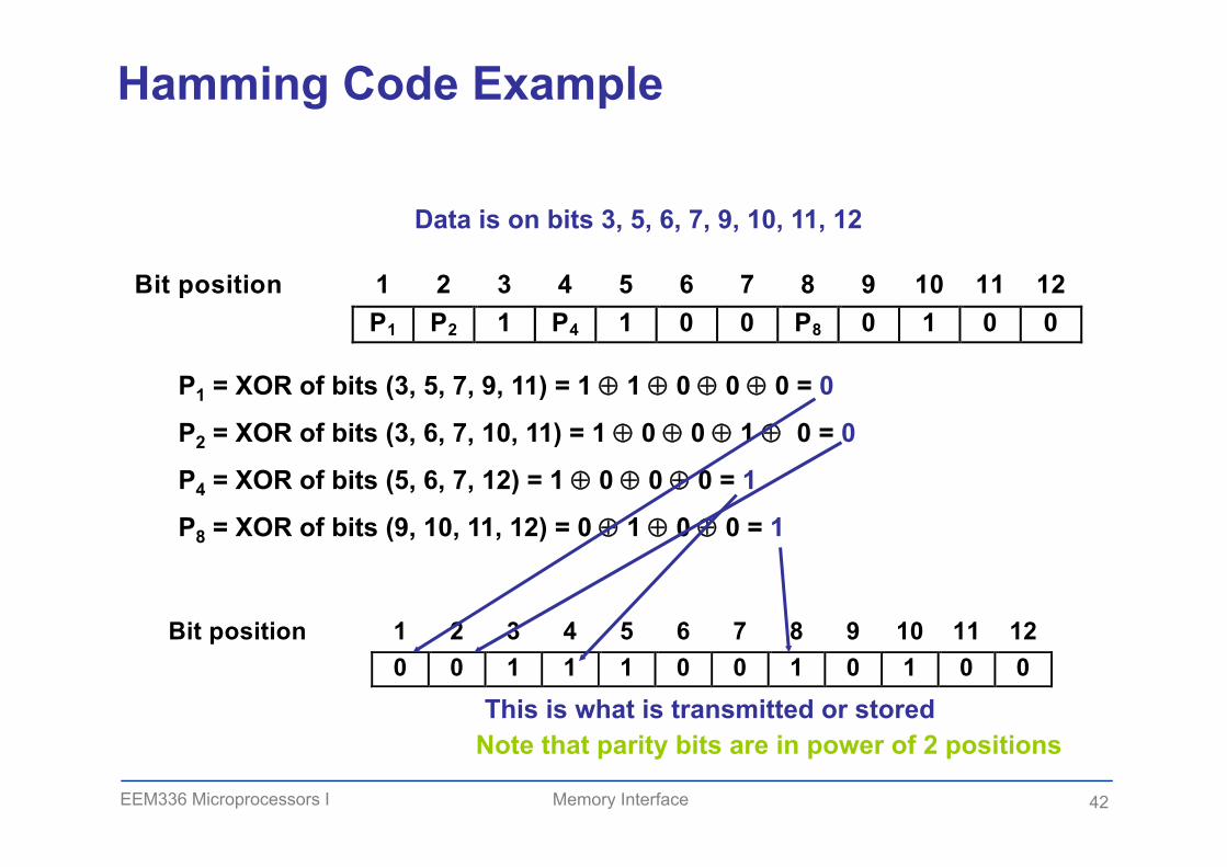
Hamming Code Example
Bit position 1 2 3 4 5 6 7 8 9 10 11 12P1 P2 1 P4 1 0 0 P8 0 1 0 0
P1 = XOR of bits (3, 5, 7, 9, 11) = 1 1 0 0 0 = 0
P2 = XOR of bits (3, 6, 7, 10, 11) = 1 0 0 1 0 = 0
P4 = XOR of bits (5, 6, 7, 12) = 1 0 0 0 = 1
P8 = XOR of bits (9, 10, 11, 12) = 0 1 0 0 = 1
Bit position 1 2 3 4 5 6 7 8 9 10 11 120 0 1 1 1 0 0 1 0 1 0 0
Data is on bits 3, 5, 6, 7, 9, 10, 11, 12
This is what is transmitted or storedNote that parity bits are in power of 2 positions
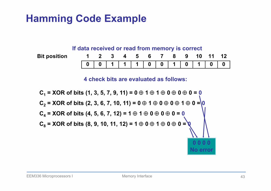
EEM336 Microprocessors I 43Memory Interface
C1 = XOR of bits (1, 3, 5, 7, 9, 11) = 0 1 1 0 0 0 = 0
C2 = XOR of bits (2, 3, 6, 7, 10, 11) = 0 1 0 0 1 0 = 0
C4 = XOR of bits (4, 5, 6, 7, 12) = 1 1 0 0 0 = 0
C8 = XOR of bits (8, 9, 10, 11, 12) = 1 0 1 0 0 = 0
If data received or read from memory is correct
0 0 0 0No error
4 check bits are evaluated as follows:
Bit position 1 2 3 4 5 6 7 8 9 10 11 120 0 1 1 1 0 0 1 0 1 0 0
Hamming Code Example

EEM336 Microprocessors I 44Memory Interface
C1 = XOR of bits (1, 3, 5, 7, 9, 11) = 0 0 1 0 0 0 = 1
C2 = XOR of bits (2, 3, 6, 7, 10, 11) = 0 0 0 0 1 0 = 1
C4 = XOR of bits (4, 5, 6, 7, 12) = 1 1 0 0 0 = 0
C8 = XOR of bits (8, 9, 10, 11, 12) = 1 0 1 0 0 = 0
If data received or read from memory is not correct
0 0 1 1Error
in bit 3
4 check bits are evaluated as follows:
Bit position 1 2 3 4 5 6 7 8 9 10 11 120 0 1 1 1 0 0 1 0 1 0 0
If read incorrectly (change bit 3 from a 1 to 0)
Bit position 1 2 3 4 5 6 7 8 9 10 11 120 0 0 1 1 0 0 1 0 1 0 0
Hamming Code Example

EEM336 Microprocessors I 45Memory Interface
The Intel Microprocessors: 8086/8088, 80186/80188, 80286, 80386, 80486 Pentium, Pentium Pro Processor, Pentium II, Pentium, 4, and Core2 with 64-bit Extensions Architecture, Programming, and Interfacing, Eighth EditionBarry B. Brey
Copyright ©2009 by Pearson Education, Inc.Upper Saddle River, New Jersey 07458 • All rights reserved.